US5523283A - La AlO3 Substrate for copper oxide superconductors - Google Patents
La AlO3 Substrate for copper oxide superconductorsDownload PDFInfo
- Publication number
- US5523283A US5523283AUS08/255,201US25520194AUS5523283AUS 5523283 AUS5523283 AUS 5523283AUS 25520194 AUS25520194 AUS 25520194AUS 5523283 AUS5523283 AUS 5523283A
- Authority
- US
- United States
- Prior art keywords
- substrate
- superconductor
- lanthanum aluminate
- superconductors
- film
- Prior art date
- Legal status (The legal status is an assumption and is not a legal conclusion. Google has not performed a legal analysis and makes no representation as to the accuracy of the status listed.)
- Expired - Fee Related
Links
Images
Classifications
- H—ELECTRICITY
- H10—SEMICONDUCTOR DEVICES; ELECTRIC SOLID-STATE DEVICES NOT OTHERWISE PROVIDED FOR
- H10N—ELECTRIC SOLID-STATE DEVICES NOT OTHERWISE PROVIDED FOR
- H10N60/00—Superconducting devices
- H10N60/10—Junction-based devices
- H10N60/12—Josephson-effect devices
- H10N60/124—Josephson-effect devices comprising high-Tc ceramic materials
- H—ELECTRICITY
- H01—ELECTRIC ELEMENTS
- H01P—WAVEGUIDES; RESONATORS, LINES, OR OTHER DEVICES OF THE WAVEGUIDE TYPE
- H01P11/00—Apparatus or processes specially adapted for manufacturing waveguides or resonators, lines, or other devices of the waveguide type
- H01P11/001—Manufacturing waveguides or transmission lines of the waveguide type
- H01P11/003—Manufacturing lines with conductors on a substrate, e.g. strip lines, slot lines
- H—ELECTRICITY
- H01—ELECTRIC ELEMENTS
- H01P—WAVEGUIDES; RESONATORS, LINES, OR OTHER DEVICES OF THE WAVEGUIDE TYPE
- H01P3/00—Waveguides; Transmission lines of the waveguide type
- H01P3/003—Coplanar lines
- H—ELECTRICITY
- H01—ELECTRIC ELEMENTS
- H01P—WAVEGUIDES; RESONATORS, LINES, OR OTHER DEVICES OF THE WAVEGUIDE TYPE
- H01P3/00—Waveguides; Transmission lines of the waveguide type
- H01P3/02—Waveguides; Transmission lines of the waveguide type with two longitudinal conductors
- H01P3/08—Microstrips; Strip lines
- H01P3/081—Microstriplines
- H—ELECTRICITY
- H10—SEMICONDUCTOR DEVICES; ELECTRIC SOLID-STATE DEVICES NOT OTHERWISE PROVIDED FOR
- H10N—ELECTRIC SOLID-STATE DEVICES NOT OTHERWISE PROVIDED FOR
- H10N60/00—Superconducting devices
- H10N60/01—Manufacture or treatment
- H10N60/0268—Manufacture or treatment of devices comprising copper oxide
- H10N60/0296—Processes for depositing or forming copper oxide superconductor layers
- H10N60/0576—Processes for depositing or forming copper oxide superconductor layers characterised by the substrate
- H10N60/0604—Monocrystalline substrates, e.g. epitaxial growth
- Y—GENERAL TAGGING OF NEW TECHNOLOGICAL DEVELOPMENTS; GENERAL TAGGING OF CROSS-SECTIONAL TECHNOLOGIES SPANNING OVER SEVERAL SECTIONS OF THE IPC; TECHNICAL SUBJECTS COVERED BY FORMER USPC CROSS-REFERENCE ART COLLECTIONS [XRACs] AND DIGESTS
- Y10—TECHNICAL SUBJECTS COVERED BY FORMER USPC
- Y10S—TECHNICAL SUBJECTS COVERED BY FORMER USPC CROSS-REFERENCE ART COLLECTIONS [XRACs] AND DIGESTS
- Y10S428/00—Stock material or miscellaneous articles
- Y10S428/922—Static electricity metal bleed-off metallic stock
- Y10S428/9265—Special properties
- Y10S428/93—Electric superconducting
- Y—GENERAL TAGGING OF NEW TECHNOLOGICAL DEVELOPMENTS; GENERAL TAGGING OF CROSS-SECTIONAL TECHNOLOGIES SPANNING OVER SEVERAL SECTIONS OF THE IPC; TECHNICAL SUBJECTS COVERED BY FORMER USPC CROSS-REFERENCE ART COLLECTIONS [XRACs] AND DIGESTS
- Y10—TECHNICAL SUBJECTS COVERED BY FORMER USPC
- Y10S—TECHNICAL SUBJECTS COVERED BY FORMER USPC CROSS-REFERENCE ART COLLECTIONS [XRACs] AND DIGESTS
- Y10S505/00—Superconductor technology: apparatus, material, process
- Y10S505/70—High TC, above 30 k, superconducting device, article, or structured stock
- Y10S505/701—Coated or thin film device, i.e. active or passive
- Y10S505/702—Josephson junction present
- Y—GENERAL TAGGING OF NEW TECHNOLOGICAL DEVELOPMENTS; GENERAL TAGGING OF CROSS-SECTIONAL TECHNOLOGIES SPANNING OVER SEVERAL SECTIONS OF THE IPC; TECHNICAL SUBJECTS COVERED BY FORMER USPC CROSS-REFERENCE ART COLLECTIONS [XRACs] AND DIGESTS
- Y10—TECHNICAL SUBJECTS COVERED BY FORMER USPC
- Y10S—TECHNICAL SUBJECTS COVERED BY FORMER USPC CROSS-REFERENCE ART COLLECTIONS [XRACs] AND DIGESTS
- Y10S505/00—Superconductor technology: apparatus, material, process
- Y10S505/70—High TC, above 30 k, superconducting device, article, or structured stock
- Y10S505/701—Coated or thin film device, i.e. active or passive
- Y10S505/703—Microelectronic device with superconducting conduction line
- Y—GENERAL TAGGING OF NEW TECHNOLOGICAL DEVELOPMENTS; GENERAL TAGGING OF CROSS-SECTIONAL TECHNOLOGIES SPANNING OVER SEVERAL SECTIONS OF THE IPC; TECHNICAL SUBJECTS COVERED BY FORMER USPC CROSS-REFERENCE ART COLLECTIONS [XRACs] AND DIGESTS
- Y10—TECHNICAL SUBJECTS COVERED BY FORMER USPC
- Y10S—TECHNICAL SUBJECTS COVERED BY FORMER USPC CROSS-REFERENCE ART COLLECTIONS [XRACs] AND DIGESTS
- Y10S505/00—Superconductor technology: apparatus, material, process
- Y10S505/70—High TC, above 30 k, superconducting device, article, or structured stock
- Y10S505/704—Wire, fiber, or cable
- Y—GENERAL TAGGING OF NEW TECHNOLOGICAL DEVELOPMENTS; GENERAL TAGGING OF CROSS-SECTIONAL TECHNOLOGIES SPANNING OVER SEVERAL SECTIONS OF THE IPC; TECHNICAL SUBJECTS COVERED BY FORMER USPC CROSS-REFERENCE ART COLLECTIONS [XRACs] AND DIGESTS
- Y10—TECHNICAL SUBJECTS COVERED BY FORMER USPC
- Y10S—TECHNICAL SUBJECTS COVERED BY FORMER USPC CROSS-REFERENCE ART COLLECTIONS [XRACs] AND DIGESTS
- Y10S505/00—Superconductor technology: apparatus, material, process
- Y10S505/825—Apparatus per se, device per se, or process of making or operating same
- Y10S505/856—Electrical transmission or interconnection system
- Y—GENERAL TAGGING OF NEW TECHNOLOGICAL DEVELOPMENTS; GENERAL TAGGING OF CROSS-SECTIONAL TECHNOLOGIES SPANNING OVER SEVERAL SECTIONS OF THE IPC; TECHNICAL SUBJECTS COVERED BY FORMER USPC CROSS-REFERENCE ART COLLECTIONS [XRACs] AND DIGESTS
- Y10—TECHNICAL SUBJECTS COVERED BY FORMER USPC
- Y10S—TECHNICAL SUBJECTS COVERED BY FORMER USPC CROSS-REFERENCE ART COLLECTIONS [XRACs] AND DIGESTS
- Y10S505/00—Superconductor technology: apparatus, material, process
- Y10S505/825—Apparatus per se, device per se, or process of making or operating same
- Y10S505/866—Wave transmission line, network, waveguide, or microwave storage device
- Y—GENERAL TAGGING OF NEW TECHNOLOGICAL DEVELOPMENTS; GENERAL TAGGING OF CROSS-SECTIONAL TECHNOLOGIES SPANNING OVER SEVERAL SECTIONS OF THE IPC; TECHNICAL SUBJECTS COVERED BY FORMER USPC CROSS-REFERENCE ART COLLECTIONS [XRACs] AND DIGESTS
- Y10—TECHNICAL SUBJECTS COVERED BY FORMER USPC
- Y10T—TECHNICAL SUBJECTS COVERED BY FORMER US CLASSIFICATION
- Y10T428/00—Stock material or miscellaneous articles
- Y10T428/24—Structurally defined web or sheet [e.g., overall dimension, etc.]
- Y10T428/24802—Discontinuous or differential coating, impregnation or bond [e.g., artwork, printing, retouched photograph, etc.]
- Y10T428/24926—Discontinuous or differential coating, impregnation or bond [e.g., artwork, printing, retouched photograph, etc.] including ceramic, glass, porcelain or quartz layer
Definitions
- This inventionrelates generally to layered perovskite superconductors and, more particularly, to substrates on which layered perovskite superconductors are deposited to form high-frequency electronic devices and circuits.
- the first material to exhibit superconductivity above the temperature of liquid nitrogenwas an oxygen-depleted layered perovskite compound of yttrium, barium, copper and oxygen, identified by the formula Y 1 Ba 2 Cu 3 O 7 . Since this discovery, other similar layered perovskite copper oxide compounds identified by the formula R 1 Ba 2 Cu 3 O 7 , where R is a rare earth element, have also been found to be superconductive at temperatures above the liquid-nitrogen temperature. This particular group of layered perovskite superconductors is commonly referred to as "1-2-3" compounds, because of the number of atoms of each metal element in the copper oxide compound.
- the major advantage of the layered perovskite superconductorsis that superconductive temperatures can be maintained using liquid nitrogen, which is considerably less expensive and troublesome than using liquid helium, as required in the past. Therefore, these superconductors can be expected to find many new applications.
- One major application already being investigatedis integrated circuits, in which thin films of these new superconductors are deposited on substrates to form, for example, Josephson junctions, waveguides and microwave transmission lines. These superconductor circuit elements can be combined to form high-speed, high-frequency and low-power integrated circuits with unparalleled performance.
- the present inventionresides in a substrate of lanthanum aluminate (LaAlO 3 ) on which thin films of layered perovskite copper oxide superconductors are formed.
- Lanthanum aluminatewith a pseudo-cubic perovskite crystal structure, has a crystal structure and lattice constant that closely match the crystal structures and lattice constants of the layered perovskite superconductors. Therefore, it promotes epitaxial film growth of the superconductors, with the crystals being oriented in the proper direction for good superconduct tire electrical properties, such as a high critical current density.
- LaAlO 3has good high frequency properties, such as a low loss tangent and low dielectric constant at superconductive temperatures.
- Lanthanum aluminatedoes not significantly interact with the superconductors. Lanthanum aluminate can also be used to form thin insulating films between the superconductor layers, which allows for the fabrication of a wide variety of superconductor circuit elements.
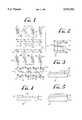
- FIG. 1illustrates the crystalline structure of a lanthanum aluminate (LaAlO 3 ) substrate on which is deposited a thin film of a layered perovskite superconductor having the formula Y 1 Ba 2 Cu 3 O 7 ;
- FIG. 2illustrates the unit cell structure of lanthanum aluminate
- FIG. 3is a fragmentary, sectional view of a Josephson junction in accordance with the present invention.
- FIG. 4is a fragmentary, sectional view of a coplanar waveguide in accordance with the present invention.
- FIG. 5is a fragmentary, sectional view of a microstrip transmission line in accordance with the. present invention.
- the present inventionis embodied in a substrate of lanthanum aluminate (LaAlO 3 ) on which thin films of layered perovskite copper oxide superconductors are formed.
- Lanthanum aluminate, with a pseudocubic perovskite crystal structurehas a crystal structure and lattice constant that closely match the crystal structures and lattice constants of the layered perovskite superconductors. Therefore, it promotes epitaxial film growth of the superconductors, with the crystals being oriented in the proper direction for good superconductive electrical properties, such as a high critical current density.
- LaAlO 3has good high frequency properties, such as a low loss tangent and low dielectric constant at superconductive temperatures.
- lanthanum aluminatedoes not significantly interact with the superconductors. Lanthanum aluminate can also used to form thin insulating films between the superconductor layers, which allows for the fabrication of a wide variety of superconductor circuit elements.
- FIG. 1illustrates the structure of a lanthanum aluminate substrate 10 on which is deposited a thin film of a layered perovskite superconductor 12 having the formula y 1 Ba 2 Cu 3 O 7 .
- each unit cell of lanthanum aluminateincludes one atom of lanthanum 14, one atom of aluminum 16 and three atoms of oxygen 18.
- the unit cellis shown as including many more aluminum and oxygen atoms, the aluminum and oxygen atoms are actually shared with adjacent unit cells.
- FIG. 1illustrates the structure of a lanthanum aluminate substrate 10 on which is deposited a thin film of a layered perovskite superconductor 12 having the formula y 1 Ba 2 Cu 3 O 7 .
- each unit cell of lanthanum aluminateincludes one atom of lanthanum 14, one atom of aluminum 16 and three atoms of oxygen 18.
- the unit cellis shown as including many more aluminum and oxygen atoms, the aluminum and oxygen
- each unit cell of the layered perovskite copper oxide superconductorincludes one atom of yttrium 20, two atoms of barium 22, three atoms of copper 24 and seven atoms of oxygen 18. Because the lattice constant of LaAlO 3 is approximately 3.80 angstroms and the lattice constant of the layered perovskite superconductor is approximately 3.85 angstroms, and because the crystalline structures of the two compounds are closely matched, the crystals of the layered perovskite superconductor orient themselves with the crystals of the lanthanum aluminate, thus providing high superconductive current flow in the direction of the arrows 26 shown in FIG. 1.
- the layered perovskite superconductorforms as layers of copper 24 and oxygen 18 atoms sandwiched between layers containing the other elements in the compound.
- Some of the copper-oxygen layersinclude planes of the atoms while other layers include chains of alternating copper and oxygen atoms.
- the layers containing the copper and oxygen atomsare the important layers for determining the superconductive electrical properties of the compound. Because the copper-oxygen layers are asymmetrically positioned in the unit cell, the compound is anisotropic in all of its electrical properties. This is why the ability of the superconductor to carry current is strongly dependent on its orientation.
- the anisotropy of the layered perovskite superconductorsis not the only problem caused by the complex chemistry and structure of these compounds.
- Each compoundcontains chemically reactive components, particularly barium, that strongly react with other substances.
- the compoundsmust be formed at very high temperatures, in the range of 700° to 950° C., to incorporate enough oxygen into the copper-oxygen layers to produce the proper crystalline structure. These high temperatures worsen the chemical reaction problems with the substrates upon which the thin films are deposited.
- One of the major advantages of LaAlO 3 as a substrate materialis that it does not significantly interact with the superconducters. Furthermore, it must undergo a large amount of chemical substitution before it loses its insulating properties.
- LaAlO 3Another of the major advantages of LaAlO 3 is its high frequency characteristics.
- the dielectric constant of LaAlO 3is less than 20, compared with 300 at room temperature and 18,000 at 4.2° K. (liquid-helium temperature) for SrTiO 3 .
- the loss tangent of LaAlO 3is 8 ⁇ 10 -5 at 77° K. and 5 ⁇ 10 -6 at 4.2°, which is comparable to that of sapphire.
- FIGS. 3, 4 and 5illustrate the use of LaAlO 3 as a substrate and as an insulating layer in several microwave circuit elements fabricated from thin films of layered perovskite copper oxide superconductors.
- FIG. 3illustrates a Josephson junction 30
- FIG. 4illustrates a coplanar waveguide 32
- FIG. 5illustrates a microstrip transmission line 34. As shown in FIG.
- the Josephson junction 30,which is the fundamental building block of superconductor electronics, includes a LaAlO 3 substrate 36, a thin film of layered perovskite superconductor 38 deposited on the substrate 36, a very thin insulating film 40 of LaAlO 3 deposited on the superconductor film 38, and another thin film of layered perovskite superconductor 42 deposited on the insulating film 40.
- the two superconductor films 38, 42are the electrodes of the Josephson junction 30 and the insulating film 40 is the barrier through which tunneling occurs. In order for tunneling to occur, the insulating film 40 must be very thin, on the order of 20-30 angstroms.
- the coplanar waveguide 32includes a LaAlO 3 substrate 44 on which are deposited a narrow thin film of layered perovskite superconductor 46 and two wide thin films of layered perovskite superconductor 48 on either side of the narrow superconductor film 46.
- the narrow superconductor film 46is the conductor of the waveguide 32 and the two wide superconductor films 48 are the walls of the waveguide.
- the microstrip transmission line 34includes a LaAlO 3 substrate 50, a thin film of layered perovskite superconductor 52 deposited on the substrate 50, a thin insulating film 54 of LaAlO 3 deposited on the superconductor film 52, and a narrow thin film of layered perovskite superconductor 56 deposited on the insulating film 54.
- the superconductor film 52is the ground plane of the microstrip transmission line 34
- the insulating film 54is the dielectric
- the superconductor film 56is the conductor.
- the insulating film 54is on the order of thousands of angstroms thick, rather than tens of angstroms, as in the Josephson junction 30.
- the microstrip transmission line 34provides nearly dispersionless, low-loss transport of high-frequency electrical signals.
- the thin insulating films of lanthanum aluminate and the thin films of the layered perovskite superconductorscan be deposited onto the LaAlO 3 substrate by one of two basic processes, both of which are conventional.
- One of the processesstarts with the superconductor compound and then deposits the compound by one of several methods onto the substrate.
- the other processstarts with the constituent elements and actually forms the compound on the substrate.
- the first processis the easiest to perform, which starts with a pellet of the compound.
- the pelletis atomized in such a way that the liberated superconductor material lands on the substrate and forms a thin film coating.
- the pelletcan be atomized using, for example, a laser (laser ablation), a stream of ions of a nonreactive gas such as argon (sputter deposition) or a vapor spray nozzle.
- rare earth chromates and other rare earth aluminates having lattice constants within a few percent of the lattice constants of the layered perovskite superconductorsshould also be suitable substrates, providing the compounds do not significantly interact with the superconductors, the compounds have good high frequency characteristics and the compounds are non-ferromagnetic and non-ferroelectric. Accordingly, the invention is not to be limited, except as by the following claims.
Landscapes
- Engineering & Computer Science (AREA)
- Manufacturing & Machinery (AREA)
- Chemical & Material Sciences (AREA)
- Crystallography & Structural Chemistry (AREA)
- Ceramic Engineering (AREA)
- Superconductor Devices And Manufacturing Methods Thereof (AREA)
- Compositions Of Oxide Ceramics (AREA)
- Inorganic Compounds Of Heavy Metals (AREA)
- Superconductors And Manufacturing Methods Therefor (AREA)
Abstract
Description
Claims (10)
Priority Applications (1)
| Application Number | Priority Date | Filing Date | Title |
|---|---|---|---|
| US08/255,201US5523283A (en) | 1988-08-18 | 1994-06-23 | La AlO3 Substrate for copper oxide superconductors |
Applications Claiming Priority (2)
| Application Number | Priority Date | Filing Date | Title |
|---|---|---|---|
| US07/233,637US5523282A (en) | 1988-08-18 | 1988-08-18 | High-frequency substrate material for thin-film layered perovskite superconductors |
| US08/255,201US5523283A (en) | 1988-08-18 | 1994-06-23 | La AlO3 Substrate for copper oxide superconductors |
Related Parent Applications (1)
| Application Number | Title | Priority Date | Filing Date |
|---|---|---|---|
| US07/233,637ContinuationUS5523282A (en) | 1988-08-18 | 1988-08-18 | High-frequency substrate material for thin-film layered perovskite superconductors |
Publications (1)
| Publication Number | Publication Date |
|---|---|
| US5523283Atrue US5523283A (en) | 1996-06-04 |
Family
ID=22878080
Family Applications (10)
| Application Number | Title | Priority Date | Filing Date |
|---|---|---|---|
| US07/233,637Expired - LifetimeUS5523282A (en) | 1988-08-18 | 1988-08-18 | High-frequency substrate material for thin-film layered perovskite superconductors |
| US07/803,935Expired - Fee RelatedUS6324413B1 (en) | 1988-08-18 | 1991-12-09 | Superconductor Josephson junction |
| US08/255,201Expired - Fee RelatedUS5523283A (en) | 1988-08-18 | 1994-06-23 | La AlO3 Substrate for copper oxide superconductors |
| US08/308,781Expired - LifetimeUS6337149B1 (en) | 1988-08-18 | 1994-09-19 | Superconductor coplanar waveguide |
| US08/334,774Expired - Fee RelatedUS5554585A (en) | 1988-08-18 | 1994-11-04 | Method of forming a superconductor microstrip transmission line |
| US08/335,000Expired - LifetimeUS5849673A (en) | 1988-08-18 | 1994-11-07 | Method of forming a superconductor coplanar waveguide |
| US08/335,232Expired - LifetimeUS6326334B1 (en) | 1988-08-18 | 1994-11-21 | Method of forming a superconductor |
| US08/369,983Expired - Fee RelatedUS6117824A (en) | 1988-08-18 | 1995-01-09 | Superconductor microstrip transmission line |
| US08/655,575Expired - LifetimeUS5906963A (en) | 1988-08-18 | 1996-05-24 | Superconductor Josephson junction comprising lanthanum aluminate |
| US09/419,993Expired - LifetimeUS6297200B1 (en) | 1988-08-18 | 1999-10-18 | High-frequency substrate material for thin-film layered perovskite superconductors |
Family Applications Before (2)
| Application Number | Title | Priority Date | Filing Date |
|---|---|---|---|
| US07/233,637Expired - LifetimeUS5523282A (en) | 1988-08-18 | 1988-08-18 | High-frequency substrate material for thin-film layered perovskite superconductors |
| US07/803,935Expired - Fee RelatedUS6324413B1 (en) | 1988-08-18 | 1991-12-09 | Superconductor Josephson junction |
Family Applications After (7)
| Application Number | Title | Priority Date | Filing Date |
|---|---|---|---|
| US08/308,781Expired - LifetimeUS6337149B1 (en) | 1988-08-18 | 1994-09-19 | Superconductor coplanar waveguide |
| US08/334,774Expired - Fee RelatedUS5554585A (en) | 1988-08-18 | 1994-11-04 | Method of forming a superconductor microstrip transmission line |
| US08/335,000Expired - LifetimeUS5849673A (en) | 1988-08-18 | 1994-11-07 | Method of forming a superconductor coplanar waveguide |
| US08/335,232Expired - LifetimeUS6326334B1 (en) | 1988-08-18 | 1994-11-21 | Method of forming a superconductor |
| US08/369,983Expired - Fee RelatedUS6117824A (en) | 1988-08-18 | 1995-01-09 | Superconductor microstrip transmission line |
| US08/655,575Expired - LifetimeUS5906963A (en) | 1988-08-18 | 1996-05-24 | Superconductor Josephson junction comprising lanthanum aluminate |
| US09/419,993Expired - LifetimeUS6297200B1 (en) | 1988-08-18 | 1999-10-18 | High-frequency substrate material for thin-film layered perovskite superconductors |
Country Status (4)
| Country | Link |
|---|---|
| US (10) | US5523282A (en) |
| EP (1) | EP0359411B1 (en) |
| JP (1) | JP2664491B2 (en) |
| DE (1) | DE68924630T2 (en) |
Cited By (5)
| Publication number | Priority date | Publication date | Assignee | Title |
|---|---|---|---|---|
| US5892243A (en)* | 1996-12-06 | 1999-04-06 | Trw Inc. | High-temperature SSNS and SNS Josephson junction and method of making junction |
| US5906963A (en)* | 1988-08-18 | 1999-05-25 | Trw Inc. | Superconductor Josephson junction comprising lanthanum aluminate |
| US5990766A (en)* | 1996-06-28 | 1999-11-23 | Superconducting Core Technologies, Inc. | Electrically tunable microwave filters |
| US6383675B1 (en) | 1999-04-20 | 2002-05-07 | Zinc Air Power Corporation | Lanthanum nickel compound/metal mixture as a third electrode in a metal-air battery |
| US6479139B1 (en)* | 1999-11-23 | 2002-11-12 | Telefonaktiebolaget Lm Ericsson (Publ) | Superconducting substrate structure and a method of producing such structure |
Families Citing this family (24)
| Publication number | Priority date | Publication date | Assignee | Title |
|---|---|---|---|---|
| US4996187A (en)* | 1988-10-17 | 1991-02-26 | Allied-Signal Inc. | Epitaxial Ba-Y-Cu-O superconductor film |
| JPH0824200B2 (en)* | 1988-11-18 | 1996-03-06 | 日本電信電話株式会社 | Tunnel junction device |
| JPH0319382A (en)* | 1989-06-16 | 1991-01-28 | Nippon Telegr & Teleph Corp <Ntt> | Tunnel junction type josephson element |
| KR920009653B1 (en)* | 1990-07-12 | 1992-10-22 | 재단법인 한국전자통신연구소 | Lanthanum aluminate thin film manufacture method |
| US5439877A (en)* | 1990-12-07 | 1995-08-08 | E. I. Du Pont De Nemours And Company | Process for depositing high temperature superconducting oxide thin films |
| EP0560941B1 (en)* | 1990-12-07 | 1996-10-16 | E.I. Du Pont De Nemours And Company | Process for depositing high temperature superconducting oxide thin films |
| JPH08255938A (en)* | 1995-01-05 | 1996-10-01 | Toshiba Corp | Superconducting wiring and semiconductor device |
| US6610633B1 (en)* | 1995-05-04 | 2003-08-26 | Trw Inc. | Superconductor device |
| US5841342A (en)* | 1995-10-13 | 1998-11-24 | Com Dev Ltd. | Voltage controlled superconducting microwave switch and method of operation thereof |
| US6004688A (en)* | 1997-07-16 | 1999-12-21 | The Board Of Regents Of The University Of Texas System | Solid oxide fuel cell and doped perovskite lanthanum gallate electrolyte therefor |
| KR100335494B1 (en)* | 1999-10-30 | 2002-05-08 | 윤종용 | Capacitor having a BST dielectric film included copper and manufacturing method thereof |
| US6839521B2 (en) | 2001-05-10 | 2005-01-04 | Northrop Grumman Corporation | Photonic bipolar modem for secure multi-channel communication |
| US6734454B2 (en) | 2001-08-27 | 2004-05-11 | The Regents Of The University Of California | Internally shunted Josephson junction device |
| US6593212B1 (en)* | 2001-10-29 | 2003-07-15 | The United States Of America As Represented By The Secretary Of The Navy | Method for making electro-optical devices using a hydrogenion splitting technique |
| US6735073B2 (en)* | 2002-01-09 | 2004-05-11 | Lucent Technologies Inc. | Electronic devices based on density wave dielectrics |
| US7700006B2 (en)* | 2002-05-31 | 2010-04-20 | Alcatel-Lucent Usa Inc. | Voltage regulators |
| US6724056B1 (en) | 2003-04-15 | 2004-04-20 | Lucent Technologies Inc. | Field-effect transistors with high-sensitivity gates |
| KR100717960B1 (en) | 2004-07-12 | 2007-05-14 | 전자부품연구원 | NanoStorage Ferroelectric Media Structure Using Superconducting Electrode |
| RU185571U1 (en)* | 2017-08-03 | 2018-12-11 | федеральное государственное бюджетное образовательное учреждение высшего образования "Ульяновский государственный университет" | Device for slowing down surface electromagnetic waves of the terahertz range based on a thin superconducting film |
| US10256392B1 (en) | 2018-03-23 | 2019-04-09 | International Business Machines Corporation | Vertical transmon qubit device |
| US10672971B2 (en) | 2018-03-23 | 2020-06-02 | International Business Machines Corporation | Vertical transmon qubit device with microstrip waveguides |
| US10243132B1 (en) | 2018-03-23 | 2019-03-26 | International Business Machines Corporation | Vertical josephson junction superconducting device |
| CN109541322B (en)* | 2018-12-13 | 2020-11-06 | 北京工业大学 | A high temperature broadband microwave material complex permittivity measurement fixture device |
| US11417821B2 (en)* | 2019-03-07 | 2022-08-16 | Northrop Grumman Systems Corporation | Superconductor ground plane patterning geometries that attract magnetic flux |
Citations (10)
| Publication number | Priority date | Publication date | Assignee | Title |
|---|---|---|---|---|
| US4421785A (en)* | 1980-08-18 | 1983-12-20 | Sperry Corporation | Superconductive tunnel junction device and method of manufacture |
| JPS6417314A (en)* | 1987-07-10 | 1989-01-20 | Matsushita Electric Industrial Co Ltd | Thin film superconductor |
| US4851794A (en)* | 1987-10-09 | 1989-07-25 | Ball Corporation | Microstrip to coplanar waveguide transitional device |
| EP0345441A2 (en)* | 1988-06-08 | 1989-12-13 | International Business Machines Corporation | High-Tc superconductor-gallate crystal structures |
| WO1990001809A1 (en)* | 1988-08-15 | 1990-02-22 | Allied-Signal Inc. | EPITAXIAL Ba-Y-Cu-O SUPERCONDUCTOR FILM ON PEROVSKITE STRUCTURE SUBSTRATE |
| US4962087A (en)* | 1988-03-04 | 1990-10-09 | Litton Systems, Inc. | Epitaxial superconducting scructure on lattice matched lanthanum orthogallate |
| US5024894A (en)* | 1988-11-02 | 1991-06-18 | Academy Of Applied Science | Method of producing silicon and similar wafers buffered for the deposition of metal oxide superconducting (MOS) polymer composites and the like by insulating metal oxides (IMO) suitable as substrates for MOS, and novel buffered wafers provided thereby |
| US5126315A (en)* | 1987-02-27 | 1992-06-30 | Hitachi, Ltd. | High tc superconducting device with weak link between two superconducting electrodes |
| US5159413A (en)* | 1990-04-20 | 1992-10-27 | Eaton Corporation | Monolithic integrated circuit having compound semiconductor layer epitaxially grown on ceramic substrate |
| US5256635A (en)* | 1988-01-15 | 1993-10-26 | University Of Arkansas | High temperature superconductor system comprising Tl2 Ba2 CuO+δ |
Family Cites Families (4)
| Publication number | Priority date | Publication date | Assignee | Title |
|---|---|---|---|---|
| US4227096A (en)* | 1978-08-31 | 1980-10-07 | Nasa | Microwave integrated circuit for Josephson voltage standards |
| US4441088A (en)* | 1981-12-31 | 1984-04-03 | International Business Machines Corporation | Stripline cable with reduced crosstalk |
| US6638894B1 (en)* | 1987-01-09 | 2003-10-28 | Lucent Technologies Inc. | Devices and systems based on novel superconducting material |
| US5523282A (en)* | 1988-08-18 | 1996-06-04 | Trw Inc. | High-frequency substrate material for thin-film layered perovskite superconductors |
- 1988
- 1988-08-18USUS07/233,637patent/US5523282A/ennot_activeExpired - Lifetime
- 1989
- 1989-08-16JPJP1211214Apatent/JP2664491B2/ennot_activeExpired - Fee Related
- 1989-08-17DEDE68924630Tpatent/DE68924630T2/ennot_activeExpired - Fee Related
- 1989-08-17EPEP89308368Apatent/EP0359411B1/ennot_activeExpired - Lifetime
- 1991
- 1991-12-09USUS07/803,935patent/US6324413B1/ennot_activeExpired - Fee Related
- 1994
- 1994-06-23USUS08/255,201patent/US5523283A/ennot_activeExpired - Fee Related
- 1994-09-19USUS08/308,781patent/US6337149B1/ennot_activeExpired - Lifetime
- 1994-11-04USUS08/334,774patent/US5554585A/ennot_activeExpired - Fee Related
- 1994-11-07USUS08/335,000patent/US5849673A/ennot_activeExpired - Lifetime
- 1994-11-21USUS08/335,232patent/US6326334B1/ennot_activeExpired - Lifetime
- 1995
- 1995-01-09USUS08/369,983patent/US6117824A/ennot_activeExpired - Fee Related
- 1996
- 1996-05-24USUS08/655,575patent/US5906963A/ennot_activeExpired - Lifetime
- 1999
- 1999-10-18USUS09/419,993patent/US6297200B1/ennot_activeExpired - Lifetime
Patent Citations (11)
| Publication number | Priority date | Publication date | Assignee | Title |
|---|---|---|---|---|
| US4421785A (en)* | 1980-08-18 | 1983-12-20 | Sperry Corporation | Superconductive tunnel junction device and method of manufacture |
| US5126315A (en)* | 1987-02-27 | 1992-06-30 | Hitachi, Ltd. | High tc superconducting device with weak link between two superconducting electrodes |
| JPS6417314A (en)* | 1987-07-10 | 1989-01-20 | Matsushita Electric Industrial Co Ltd | Thin film superconductor |
| US4851794A (en)* | 1987-10-09 | 1989-07-25 | Ball Corporation | Microstrip to coplanar waveguide transitional device |
| US5256635A (en)* | 1988-01-15 | 1993-10-26 | University Of Arkansas | High temperature superconductor system comprising Tl2 Ba2 CuO+δ |
| US4962087A (en)* | 1988-03-04 | 1990-10-09 | Litton Systems, Inc. | Epitaxial superconducting scructure on lattice matched lanthanum orthogallate |
| EP0345441A2 (en)* | 1988-06-08 | 1989-12-13 | International Business Machines Corporation | High-Tc superconductor-gallate crystal structures |
| WO1990001809A1 (en)* | 1988-08-15 | 1990-02-22 | Allied-Signal Inc. | EPITAXIAL Ba-Y-Cu-O SUPERCONDUCTOR FILM ON PEROVSKITE STRUCTURE SUBSTRATE |
| US5030613A (en)* | 1988-08-15 | 1991-07-09 | Allied-Signal Inc. | Epitaxial Ba--Y--Cu--O ceramic superconductor film on perovskite structure substrate |
| US5024894A (en)* | 1988-11-02 | 1991-06-18 | Academy Of Applied Science | Method of producing silicon and similar wafers buffered for the deposition of metal oxide superconducting (MOS) polymer composites and the like by insulating metal oxides (IMO) suitable as substrates for MOS, and novel buffered wafers provided thereby |
| US5159413A (en)* | 1990-04-20 | 1992-10-27 | Eaton Corporation | Monolithic integrated circuit having compound semiconductor layer epitaxially grown on ceramic substrate |
Non-Patent Citations (109)
| Title |
|---|
| "Superconductors' Material Problems," Science, vol. 240, Apr. 1, 1988, pp. 25-27. |
| "Theoretical Resistance,"Scientific American, Dec., 1992, pp. 24-25. |
| Amato, "High-T Superconductors Get Squeezed," Science, vol. 261, Oct. 1, 1993, pp. 31. |
| Amato, High T Superconductors Get Squeezed, Science, vol. 261, Oct. 1, 1993, pp. 31.* |
| Bednorz, J. G., et al., "Phase Diagram of the (La103)1-x (Sr TiO3) x Solid-solution System, for x ≦ 0.8," Mat. Res. Bull., 18:181-187 (1983). |
| Bednorz, J. G., et al., Phase Diagram of the (La10 3 ) 1 x (Sr TiO 3) x Solid solution System, for x 0.8, Mat. Res. Bull., 18:181 187 (1983).* |
| Belt, R. F., et al., "Investigation of LaAl1-x Scx 03 for a Laser Host," Journal of Crystal Growth, 70:471-475 (1984). |
| Belt, R. F., et al., Investigation of LaAl 1 x Sc x 0 3 for a Laser Host, Journal of Crystal Growth, 70:471 475 (1984).* |
| Brandle, C. D., "Czochralski Growth of LaAlO3," Final Report, Union Carbide Corporation (Jul. 29, 1969) pp.1-6. |
| Brandle, C. D., Czochralski Growth of LaAlO 3, Final Report, Union Carbide Corporation (Jul. 29, 1969) pp.1 6.* |
| Brown, R., et al., "Low-loss Substrate for Microwave Application of High-temperature Superconductor Films," Applied Physics Letter, 57(13):1351-1353 (1990). |
| Brown, R., et al., Low loss Substrate for Microwave Application of High temperature Superconductor Films, Applied Physics Letter, 57(13):1351 1353 (1990).* |
| Cava, R. J., et al., "Bulk Superconductivity at 36 k in La1.8 Sr0.2 Cu04," The American Physical Society, Physical Review Letters, 58(4):408-410 (Jan. 26, 1987). |
| Cava, R. J., et al., Bulk Superconductivity at 36 k in La 1.8 Sr 0.2 Cu0 4, The American Physical Society, Physical Review Letters, 58(4):408 410 (Jan. 26, 1987).* |
| Cuprate Superconductors, Record 133 K Achieved with Mercury, May 10, 1993, C&EN, pp. 4.* |
| Doss, "Engineer's Guide to High Temperature Superconductivity," Wiley & Sons, 1989, pp. 104-109 and 152-157. |
| Doss, Engineer s Guide to High Temperature Superconductivity, Wiley & Sons, 1989, pp. 104 109 and 152 157.* |
| Edelstein, et al., "Formation of the Structure of the Superconducting Phase of La-Sr-Cu-o by DC Sputtering," J. Crystal Growth, 85:619-622 (1987). |
| Edelstein, et al., Formation of the Structure of the Superconducting Phase of La Sr Cu o by DC Sputtering, J. Crystal Growth, 85:619 622 (1987).* |
| Faucher, M., et al., "Optical Study of LaAlO3 :Eu at Temperatures Approaching the Rhombohedric→Cubic Transition," The Journal of Chemical Physics, 63(1):446-454 (1975). |
| Faucher, M., et al., Optical Study of LaAlO 3 :Eu at Temperatures Approaching the Rhombohedric Cubic Transition, The Journal of Chemical Physics, 63(1):446 454 (1975).* |
| Fisk, et al., "Superconductivity of Rare Earth-Barium-Copper Oxides," Solid State Communications, vol. 62, No. 11, pp. 743-744, 1987. |
| Fisk, et al., Superconductivity of Rare Earth Barium Copper Oxides, Solid State Communications, vol. 62, No. 11, pp. 743 744, 1987.* |
| Fritsche, E. T., et al., "Liquidus in the Alumina-rich System La2 O3 -Al2 O3," Journal of the American Ceramic Society, 50(3):167-168 (1967). |
| Fritsche, E. T., et al., Liquidus in the Alumina rich System La 2 O 3 Al 2 O 3, Journal of the American Ceramic Society, 50(3):167 168 (1967).* |
| Fulton, T. A., et al., "The Flux Shuttle-A Josephson Junction Shift Register Employing Single Flux Quanta," Proceedings of the IEEE, 61(1):28-35 (1973). |
| Fulton, T. A., et al., The Flux Shuttle A Josephson Junction Shift Register Employing Single Flux Quanta, Proceedings of the IEEE, 61(1):28 35 (1973).* |
| Gaballe, "Paths to Higher Temperature Superconductors," Science, vol. 259, Mar. 12, 1993, pp. 1550-1551. |
| Gaballe, Paths to Higher Temperature Superconductors, Science, vol. 259, Mar. 12, 1993, pp. 1550 1551.* |
| Geller, S., "Crystallographic Studies of Perovskite-like Compounds. IV. Rare Earth Scandates, Vanadites, Galliates, Orthochromites," Acta Cryst., 10:243-428 (1957). |
| Geller, S., Crystallographic Studies of Perovskite like Compounds. IV. Rare Earth Scandates, Vanadites, Galliates, Orthochromites, Acta Cryst., 10:243 428 (1957).* |
| Geller, S., et al., "Crystallographic Studies of Perovskite-like Compounds. II. Rare Earth Aluminates," Acta. Cryst., 9:1019-1025 (1956). |
| Geller, S., et al., Crystallographic Studies of Perovskite like Compounds. II. Rare Earth Aluminates, Acta. Cryst., 9:1019 1025 (1956).* |
| Gulysev, Yu V., et al., "YBa2 CU3 07-x Films with a High-temperature Superconductivity Synthesized by Magnetron Sputtering," Sov. Tech. Phys. Lett., 14(4):339-340 (Apr. 1988). |
| Gulysev, Yu V., et al., YBa 2 CU 3 0 7 x Films with a High temperature Superconductivity Synthesized by Magnetron Sputtering, Sov. Tech. Phys. Lett., 14(4):339 340 (Apr. 1988).* |
| Gurvitch, M., et al., "Preparation and Substrate Reactions of Superconducting Y-Ba-Cu-O Films," Appl. Phys. Lett., 51(13):1027-1029 (1987). |
| Gurvitch, M., et al., Preparation and Substrate Reactions of Superconducting Y Ba Cu O Films, Appl. Phys. Lett., 51(13):1027 1029 (1987).* |
| H hler, A., et al., Fully Textured Growth of Y 1 Ba 2 Cu 3 O 7 d Films by Sputtering on LiNbO 3 Substrates, Appl Phys. Lett., 54(11):1066 1067 (1989).* |
| Hashimoto, T., et al., "Thermal Expansion Coefficients of High-Tc Superconductors," Japanese Journal of Applied Physics, 27(2):L214-L216 (1988). |
| Hashimoto, T., et al., Thermal Expansion Coefficients of High T c Superconductors, Japanese Journal of Applied Physics, 27(2):L214 L216 (1988).* |
| Hazen, et al., "100-K Superconducting Phases in the Tl-Ca-Ba-Cu-O System," Physical Review Letters, vol. 60, No. 16, Apr. 18, 1988, pp. 1657-1660. |
| Hazen, et al., 100 K Superconducting Phases in the Tl Ca Ba Cu O System, Physical Review Letters, vol. 60, No. 16, Apr. 18, 1988, pp. 1657 1660.* |
| Hohler, A., et al., "Fully Textured Growth of Y1 Ba2 Cu3 O7-d Films by Sputtering on LiNbO3 Substrates," Appl Phys. Lett., 54(11):1066-1067 (1989). |
| Holstein, W. L., et al., "Effect of Single Crystal Substrates on the Growth and Properties of Superconducting TI2 Ba2 CaCu2 O8 Films," J. Mater. Res., 8(5):962-972 (May 1993). |
| Holstein, W. L., et al., Effect of Single Crystal Substrates on the Growth and Properties of Superconducting TI 2 Ba 2 CaCu 2 O 8 Films, J. Mater. Res., 8(5):962 972 (May 1993).* |
| Kilner, J. A., et al., "Electrolytes for the High Temperature Fuel Cell; Experimental and Theoretical Studies of the Perovskite LaAlO3," Journal of Power Sources, 3:67-80 (1978). |
| Kilner, J. A., et al., Electrolytes for the High Temperature Fuel Cell; Experimental and Theoretical Studies of the Perovskite LaAlO 3, Journal of Power Sources, 3:67 80 (1978).* |
| Koinuma, H., et al., "Chemical Interaction between Ba2 YCu3 O7-d and Substrate Materials in the Solid State," Japanese Journal of Applied Physics, 27(7):L1216-L1218 (1988). |
| Koinuma, H., et al., "Some Problems in the Preparation of Superconducting Oxide Films on Ceramic Substrates," Japanese Journal of Applied Physics, 26(5):L763-L765 (1987). |
| Koinuma, H., et al., Chemical Interaction between Ba 2 YCu 3 O 7 d and Substrate Materials in the Solid State, Japanese Journal of Applied Physics, 27(7):L1216 L1218 (1988).* |
| Koinuma, H., et al., Some Problems in the Preparation of Superconducting Oxide Films on Ceramic Substrates, Japanese Journal of Applied Physics, 26(5):L763 L765 (1987).* |
| Kondoh, et al., "Superconductivity in Tl-Ba-Cu-O System," Solid State Communications, vol. 65, No. 11, pp. 1329-1331, 1988. |
| Kondoh, et al., Superconductivity in Tl Ba Cu O System, Solid State Communications, vol. 65, No. 11, pp. 1329 1331, 1988.* |
| Koren, G., et al., "Epitaxial Films of YBa2 Cu3 O7-d on NdGaO3, LaGaO3, and SrTio3 Substrates Deposited by Laser Ablation," Applied Physics Letter, 54(11):1054-1056 (1989). |
| Koren, G., et al., Epitaxial Films of YBa 2 Cu 3 O 7 d on NdGaO 3 , LaGaO 3 , and SrTio 3 Substrates Deposited by Laser Ablation, Applied Physics Letter, 54(11):1054 1056 (1989).* |
| Kotru, P. N., et al., "Optical Microscopic Studies on Grown and Etched Surfaces of Flux Grown LaAlO3 Crystals," Journal of Materials Science, 20:3365-3374 (1985). |
| Kotru, P. N., et al., Optical Microscopic Studies on Grown and Etched Surfaces of Flux Grown LaAlO 3 Crystals, Journal of Materials Science, 20:3365 3374 (1985).* |
| Kumar, A., et al., "Textured Superconducting Thin Films of Bismuth Caprate by Laser Ablation Method," Mat. Res. Soc. Symp. Proc., 169:527-532 (1990). |
| Kumar, A., et al., Textured Superconducting Thin Films of Bismuth Caprate by Laser Ablation Method, Mat. Res. Soc. Symp. Proc., 169:527 532 (1990).* |
| Laville, F., et al., "Optical and ESR Investigations of Lanthanum Aluminates LaMg1-x Mnx O19 Single Crystals with Magnetoplumbite-like Structure," Journal of Solid State Chemistry, 49:180-187 (1983). |
| Laville, F., et al., Optical and ESR Investigations of Lanthanum Aluminates LaMg 1 x Mn x O 19 Single Crystals with Magnetoplumbite like Structure, Journal of Solid State Chemistry, 49:180 187 (1983).* |
| Lechter, et al., "Bulk Superconductivity Above 100 K in the Tl-Sr-Ca-Cu System," Solid State Communications, vol. 68, No. 6, pp. 519-521, 1988. |
| Lechter, et al., Bulk Superconductivity Above 100 K in the Tl Sr Ca Cu System, Solid State Communications, vol. 68, No. 6, pp. 519 521, 1988.* |
| Lee, A. E., et al., "Epitaxially Grown Sputtered LaAlO3 Films," Applied Physics Letter, 57(19):2019-2021 (1990). |
| Lee, A. E., et al., Epitaxially Grown Sputtered LaAlO 3 Films, Applied Physics Letter, 57(19):2019 2021 (1990).* |
| M ller, K. A., Critical Phenomena Near Structural Phase Transitions Studied by EPR, Ferroelectrics, 7:17 21 (1974).* |
| Maidukova, T. P., et al., "Formation of Lanthanum Aluminate in the Copercipitation of Carbonate and Hydroxide Compounds of Lanthanum and Aluminum," Russian Journal of Inorganic Chemistry, 22(11):1622-1625 (1977). |
| Maidukova, T. P., et al., Formation of Lanthanum Aluminate in the Copercipitation of Carbonate and Hydroxide Compounds of Lanthanum and Aluminum, Russian Journal of Inorganic Chemistry, 22(11):1622 1625 (1977).* |
| Mannhart, J., et al., "Micropatterning of High Tc Films with an Excimer Laser," Appl. Phys. Lett., 52(15):1271-1273 (Apr. 1988). |
| Mannhart, J., et al., Micropatterning of High T c Films with an Excimer Laser, Appl. Phys. Lett., 52(15):1271 1273 (Apr. 1988).* |
| Menyhard, N., "Multicritical Behavior in LaA103,"Solid State Comm., 52(1):31-35 (1984). |
| Menyhard, N., Multicritical Behavior in LaA10 3 , Solid State Comm., 52(1):31 35 (1984).* |
| Muller, K. A., "Critical Phenomena Near Structural Phase Transitions Studied by EPR," Ferroelectrics, 7:17-21 (1974). |
| Osofsky, et al., "Superconductivity in Thin Films of Bi-Sr Cu Cu-O Prepared by a Simple Flash Evaporation Technique and Bulk Superconductivity Above 100 K in a New Copper Oxide Compound," MRS Int'l. Mtg. on Adv. Mats., vol. 6, 1989, Materials Research Society pp. 669-674. |
| Osofsky, et al., Superconductivity in Thin Films of Bi Sr Cu Cu O Prepared by a Simple Flash Evaporation Technique and Bulk Superconductivity Above 100 K in a New Copper Oxide Compound, MRS Int l. Mtg. on Adv. Mats., vol. 6, 1989, Materials Research Society pp. 669 674.* |
| Pamplin, Editor, "Crystal Growth", pp. 248-249, Pergamon Press, New York (1975). |
| Pamplin, Editor, Crystal Growth , pp. 248 249, Pergamon Press, New York (1975).* |
| Ropp, R. C., et al., "Solid-State Kinetics of LaAl11 O18," Journal of American Ceramic Society, 63(7-8):416-419 (Jul.-Aug. 1980). |
| Ropp, R. C., et al., "The Nature of the Alumina-rich Phase in the System La2 O3 -Al2 O3," Journal of American Ceramic Society, 61(11-12):473-475 (1978). |
| Ropp, R. C., et al., Solid State Kinetics of LaAl 11 O 18 , Journal of American Ceramic Society, 63(7 8):416 419 (Jul. Aug. 1980).* |
| Ropp, R. C., et al., The Nature of the Alumina rich Phase in the System La 2 O 3 Al 2 O 3 , Journal of American Ceramic Society, 61(11 12):473 475 (1978).* |
| Sandstrom, R. L., et al., "Lanthanum Gallate Substrates for Epitaxial High-temperature Superconducting Thin Films," Applied Physics Letter, 53(19):1874-1876 (1988). |
| Sandstrom, R. L., et al., Lanthanum Gallate Substrates for Epitaxial High temperature Superconducting Thin Films, Applied Physics Letter, 53(19):1874 1876 (1988).* |
| Scott, W. B., "U.S. to Push Aerospace Research, but May Stymie Efforts to Export Products", Aviation Week & Space Technology, pp. 39-40 (Mar. 16, 1992). |
| Scott, W. B., U.S. to Push Aerospace Research, but May Stymie Efforts to Export Products , Aviation Week & Space Technology, pp. 39 40 (Mar. 16, 1992).* |
| Simon et al "Low-Loss Substrate for Epitaxial Growth of High-Temperature Superconductor Thin Films", Appl. Phys. Lett. 53(26) Dec. 1988 pp. 2677-2679. |
| Simon et al Low Loss Substrate for Epitaxial Growth of High Temperature Superconductor Thin Films , Appl. Phys. Lett. 53(26) Dec. 1988 pp. 2677 2679.* |
| Simon, R. W., et al., "Improvement of Average Film Quality in RBa2 Cu3 O7-x Sputtered Films," IEEE Transactions on Magnetics, 25(2):2433-2436 (Mar. 1989). |
| Simon, R. W., et al., "Low-Loss Substrate for Epitaxial Growth of High-temperature Superconductor Thin Films," Applied Physics Letters, 53(26):2677-2679 (Dec. 1988). |
| Simon, R. W., et al., Improvement of Average Film Quality in RBa 2 Cu 3 O 7 x Sputtered Films, IEEE Transactions on Magnetics, 25(2):2433 2436 (Mar. 1989).* |
| Simon, R. W., et al., Low Loss Substrate for Epitaxial Growth of High temperature Superconductor Thin Films, Applied Physics Letters, 53(26):2677 2679 (Dec. 1988).* |
| Smith, S. H. et al., "The Growth of LaAlO3 Crystals Enriched in Isotope 17 O," Journal of Crystal Growth, 47:315-316 (1979). |
| Smith, S. H. et al., The Growth of LaAlO 3 Crystals Enriched in Isotope 17 O, Journal of Crystal Growth, 47:315 316 (1979).* |
| Superconductors Material Problems, Science, vol. 240, Apr. 1, 1988, pp. 25 27.* |
| Takemoto, J. H., "Microstrip Resonators and Filters Using High-TC Superconducting Thin Films on LaAlO3," TRW Space and Technology Group, Redondo Beach, Calif. (1990) pp. 1-4. |
| Takemoto, J. H., Microstrip Resonators and Filters Using High TC Superconducting Thin Films on LaAlO 3 , TRW Space and Technology Group, Redondo Beach, Calif. (1990) pp. 1 4.* |
| Tamegai, et al, "Structures and Upper Critical Fields of High Tc Superconductors (RE)Ba2 Cu3 Ox," Japanese Journal of Applied Physics, vol. 26, No. 8, Aug., 1987, pp. L1304-L1306. |
| Tamegai, et al, Structures and Upper Critical Fields of High T c Superconductors (RE)Ba 2 Cu 3 O x , Japanese Journal of Applied Physics, vol. 26, No. 8, Aug., 1987, pp. L1304 L1306.* |
| Taylor, D., "Thermal Expansion Data VIII. Complex Oxides, ABO3, the Perovskites," Journal of Thermal Expansion Data, vol. 84, No. 6 (1985). |
| Taylor, D., Thermal Expansion Data VIII. Complex Oxides, ABO 3 , the Perovskites, Journal of Thermal Expansion Data, vol. 84, No. 6 (1985).* |
| Theoretical Resistance, Scientific American, Dec., 1992, pp. 24 25.* |
| Williams, et al., "Chemical Compatibility of High-temperature Superconductors with Other Materials," American Chemical Society, Washington, D.C. 1988, pp. 291-302. |
| Williams, et al., Chemical Compatibility of High temperature Superconductors with Other Materials, American Chemical Society, Washington, D.C. 1988, pp. 291 302.* |
| Xiao, et al., "Magnetic Characteristics of Superconducting RBa2 Cu3 O6+y (R=Nd, Sm, Eu, Gd, Dy, Ho, Er, Tm, and Yb)," Solid State Communications, vol. 63, No. 9, 1987, pp. 817-810. |
| Xiao, et al., Magnetic Characteristics of Superconducting RBa 2 Cu 3 O 6 y (R Nd, Sm, Eu, Gd, Dy, Ho, Er, Tm, and Yb), Solid State Communications, vol. 63, No. 9, 1987, pp. 817 810.* |
| Yajima, S., et al., "Synthesis of Lanthanoid Aluminates (β-Al2 O3 Type) Using Arc Plasma Flame," Chemistry Letters, pp. 1331-1334 (Japan 1973). |
| Yajima, S., et al., Synthesis of Lanthanoid Aluminates ( Al 2 O 3 Type) Using Arc Plasma Flame, Chemistry Letters, pp. 1331 1334 (Japan 1973).* |
| Yamaguchi, O., et al., "New Compound in the System La2 O3 -Al2 O3," Communications of the American Ceramic Society, 68(2):C-44-45 (1985). |
| Yamaguchi, O., et al., New Compound in the System La 2 O 3 Al 2 O 3 , Communications of the American Ceramic Society, 68(2):C 44 45 (1985).* |
Cited By (7)
| Publication number | Priority date | Publication date | Assignee | Title |
|---|---|---|---|---|
| US5906963A (en)* | 1988-08-18 | 1999-05-25 | Trw Inc. | Superconductor Josephson junction comprising lanthanum aluminate |
| US5990766A (en)* | 1996-06-28 | 1999-11-23 | Superconducting Core Technologies, Inc. | Electrically tunable microwave filters |
| US6097263A (en)* | 1996-06-28 | 2000-08-01 | Robert M. Yandrofski | Method and apparatus for electrically tuning a resonating device |
| US5892243A (en)* | 1996-12-06 | 1999-04-06 | Trw Inc. | High-temperature SSNS and SNS Josephson junction and method of making junction |
| US6066600A (en)* | 1996-12-06 | 2000-05-23 | Trw Inc. | Method of making high-Tc SSNS and SNS Josephson junction |
| US6383675B1 (en) | 1999-04-20 | 2002-05-07 | Zinc Air Power Corporation | Lanthanum nickel compound/metal mixture as a third electrode in a metal-air battery |
| US6479139B1 (en)* | 1999-11-23 | 2002-11-12 | Telefonaktiebolaget Lm Ericsson (Publ) | Superconducting substrate structure and a method of producing such structure |
Also Published As
| Publication number | Publication date |
|---|---|
| US6297200B1 (en) | 2001-10-02 |
| EP0359411A2 (en) | 1990-03-21 |
| US6324413B1 (en) | 2001-11-27 |
| JPH0291982A (en) | 1990-03-30 |
| US6326334B1 (en) | 2001-12-04 |
| US6337149B1 (en) | 2002-01-08 |
| DE68924630T2 (en) | 1996-04-04 |
| US6117824A (en) | 2000-09-12 |
| US5906963A (en) | 1999-05-25 |
| DE68924630D1 (en) | 1995-11-30 |
| JP2664491B2 (en) | 1997-10-15 |
| US5849673A (en) | 1998-12-15 |
| US5554585A (en) | 1996-09-10 |
| EP0359411A3 (en) | 1990-03-28 |
| US5523282A (en) | 1996-06-04 |
| EP0359411B1 (en) | 1995-10-25 |
Similar Documents
| Publication | Publication Date | Title |
|---|---|---|
| US5523283A (en) | La AlO3 Substrate for copper oxide superconductors | |
| US5538941A (en) | Superconductor/insulator metal oxide hetero structure for electric field tunable microwave device | |
| Lathrop et al. | Production of YBa2Cu3O7− y superconducting thin films in situ by high‐pressure reactive evaporation and rapid thermal annealing | |
| US6498549B1 (en) | Dual-tuning microwave devices using ferroelectric/ferrite layers | |
| US5627139A (en) | High-temperature superconducting josephson devices having a barrier layer of a doped, cubic crystalline, conductive oxide material | |
| US5593951A (en) | Epitaxy of high TC superconductors on silicon | |
| CN1022654C (en) | Tunnel type Josephson device and manufacturing method thereof | |
| US5604375A (en) | Superconducting active lumped component for microwave device application | |
| US5179070A (en) | Semiconductor substrate having a superconducting thin film with a buffer layer in between | |
| EP0567407B1 (en) | Microwave component of oxide superconducter material | |
| US5814584A (en) | Compound in the series A2 MeSbO6 for use as substrates barrier-dielectric layers and passivating layers in high critical temperature superconducting devices | |
| US4996185A (en) | Ceramic superconducting thin film | |
| Hermann et al. | Oxide superconductors and ferroelectrics—Materials for a new generation of tunable microwave devices | |
| US5250506A (en) | Superconductive switching element with semiconductor channel | |
| US5342828A (en) | Superconducting Tl-Pb-Sr-Ca-Cu-O thin film | |
| EP0341148B1 (en) | A semiconductor substrate having a superconducting thin film | |
| EP0508893A1 (en) | Substrate for microwave component | |
| US6610633B1 (en) | Superconductor device | |
| US5296458A (en) | Epitaxy of high Tc superconducting films on (001) silicon surface | |
| US5051398A (en) | Process for preparing a bismuth-type superconducting thin film | |
| JP2501035B2 (en) | Superconducting thin film | |
| US7192661B1 (en) | Rare earth metal compounds for use in high critical temperature thin film super-conducting antennas | |
| EP0517560B1 (en) | Method of manufacturing a superconducting microwave component substrate | |
| US6156707A (en) | Method of manufacturing superconducting microwave component substrate | |
| US5362709A (en) | Superconducting device |
Legal Events
| Date | Code | Title | Description |
|---|---|---|---|
| CC | Certificate of correction | ||
| FPAY | Fee payment | Year of fee payment:4 | |
| FEPP | Fee payment procedure | Free format text:PAYOR NUMBER ASSIGNED (ORIGINAL EVENT CODE: ASPN); ENTITY STATUS OF PATENT OWNER: LARGE ENTITY | |
| AS | Assignment | Owner name:NORTHROP GRUMMAN CORPORATION, CALIFORNIA Free format text:ASSIGNMENT OF ASSIGNORS INTEREST;ASSIGNOR:TRW, INC. N/K/A NORTHROP GRUMMAN SPACE AND MISSION SYSTEMS CORPORATION, AN OHIO CORPORATION;REEL/FRAME:013751/0849 Effective date:20030122 Owner name:NORTHROP GRUMMAN CORPORATION,CALIFORNIA Free format text:ASSIGNMENT OF ASSIGNORS INTEREST;ASSIGNOR:TRW, INC. N/K/A NORTHROP GRUMMAN SPACE AND MISSION SYSTEMS CORPORATION, AN OHIO CORPORATION;REEL/FRAME:013751/0849 Effective date:20030122 | |
| FPAY | Fee payment | Year of fee payment:8 | |
| REMI | Maintenance fee reminder mailed | ||
| LAPS | Lapse for failure to pay maintenance fees | ||
| STCH | Information on status: patent discontinuation | Free format text:PATENT EXPIRED DUE TO NONPAYMENT OF MAINTENANCE FEES UNDER 37 CFR 1.362 | |
| FP | Lapsed due to failure to pay maintenance fee | Effective date:20080604 |