US5519235A - Polycrystalline ferroelectric capacitor heterostructure employing hybrid electrodes - Google Patents
Polycrystalline ferroelectric capacitor heterostructure employing hybrid electrodesDownload PDFInfo
- Publication number
- US5519235A US5519235AUS08/341,728US34172894AUS5519235AUS 5519235 AUS5519235 AUS 5519235AUS 34172894 AUS34172894 AUS 34172894AUS 5519235 AUS5519235 AUS 5519235A
- Authority
- US
- United States
- Prior art keywords
- layer
- ferroelectric
- strontium
- titanate
- grown
- Prior art date
- Legal status (The legal status is an assumption and is not a legal conclusion. Google has not performed a legal analysis and makes no representation as to the accuracy of the status listed.)
- Expired - Fee Related
Links
- 239000003990capacitorSubstances0.000titleclaimsabstractdescription13
- 239000000463materialSubstances0.000claimsabstractdescription16
- 239000000758substrateSubstances0.000claimsabstractdescription15
- BASFCYQUMIYNBI-UHFFFAOYSA-NplatinumChemical compound[Pt]BASFCYQUMIYNBI-UHFFFAOYSA-N0.000claimsabstractdescription14
- 229910044991metal oxideInorganic materials0.000claimsabstractdescription12
- 229910052697platinumInorganic materials0.000claimsabstractdescription5
- 239000010410layerSubstances0.000claimsdescription55
- VYPSYNLAJGMNEJ-UHFFFAOYSA-NSilicium dioxideChemical compoundO=[Si]=OVYPSYNLAJGMNEJ-UHFFFAOYSA-N0.000claimsdescription24
- 229910021320cobalt-lanthanum-strontium oxideInorganic materials0.000claimsdescription18
- 239000000377silicon dioxideSubstances0.000claimsdescription12
- 238000000034methodMethods0.000claimsdescription11
- 229910052751metalInorganic materials0.000claimsdescription8
- 239000002184metalSubstances0.000claimsdescription8
- GWEVSGVZZGPLCZ-UHFFFAOYSA-NTitan oxideChemical compoundO=[Ti]=OGWEVSGVZZGPLCZ-UHFFFAOYSA-N0.000claimsdescription6
- VNSWULZVUKFJHK-UHFFFAOYSA-N[Sr].[Bi]Chemical compound[Sr].[Bi]VNSWULZVUKFJHK-UHFFFAOYSA-N0.000claimsdescription6
- 239000010936titaniumSubstances0.000claimsdescription6
- RTAQQCXQSZGOHL-UHFFFAOYSA-NTitaniumChemical compound[Ti]RTAQQCXQSZGOHL-UHFFFAOYSA-N0.000claimsdescription5
- XUIMIQQOPSSXEZ-UHFFFAOYSA-NSiliconChemical compound[Si]XUIMIQQOPSSXEZ-UHFFFAOYSA-N0.000claimsdescription4
- 229910002115bismuth titanateInorganic materials0.000claimsdescription4
- 229910052710siliconInorganic materials0.000claimsdescription4
- 239000010703siliconSubstances0.000claimsdescription4
- ZLMJMSJWJFRBEC-UHFFFAOYSA-NPotassiumChemical compound[K]ZLMJMSJWJFRBEC-UHFFFAOYSA-N0.000claimsdescription3
- GGGMJWBVJUTTLO-UHFFFAOYSA-N[Co]=O.[Sr].[La]Chemical compound[Co]=O.[Sr].[La]GGGMJWBVJUTTLO-UHFFFAOYSA-N0.000claimsdescription3
- QVGXLLKOCUKJST-UHFFFAOYSA-Natomic oxygenChemical compound[O]QVGXLLKOCUKJST-UHFFFAOYSA-N0.000claimsdescription3
- 229910052454barium strontium titanateInorganic materials0.000claimsdescription3
- 229910002113barium titanateInorganic materials0.000claimsdescription3
- JRPBQTZRNDNNOP-UHFFFAOYSA-Nbarium titanateChemical compound[Ba+2].[Ba+2].[O-][Ti]([O-])([O-])[O-]JRPBQTZRNDNNOP-UHFFFAOYSA-N0.000claimsdescription3
- NKZSPGSOXYXWQA-UHFFFAOYSA-Ndioxido(oxo)titanium;lead(2+)Chemical compound[Pb+2].[O-][Ti]([O-])=ONKZSPGSOXYXWQA-UHFFFAOYSA-N0.000claimsdescription3
- 229910052746lanthanumInorganic materials0.000claimsdescription3
- FZLIPJUXYLNCLC-UHFFFAOYSA-Nlanthanum atomChemical compound[La]FZLIPJUXYLNCLC-UHFFFAOYSA-N0.000claimsdescription3
- 229910052758niobiumInorganic materials0.000claimsdescription3
- 239000010955niobiumSubstances0.000claimsdescription3
- GUCVJGMIXFAOAE-UHFFFAOYSA-Nniobium atomChemical compound[Nb]GUCVJGMIXFAOAE-UHFFFAOYSA-N0.000claimsdescription3
- 229910052760oxygenInorganic materials0.000claimsdescription3
- 239000001301oxygenSubstances0.000claimsdescription3
- 229910052700potassiumInorganic materials0.000claimsdescription3
- 239000011591potassiumSubstances0.000claimsdescription3
- 229910052581Si3N4Inorganic materials0.000claimsdescription2
- HQVNEWCFYHHQES-UHFFFAOYSA-Nsilicon nitrideChemical compoundN12[Si]34N5[Si]62N3[Si]51N64HQVNEWCFYHHQES-UHFFFAOYSA-N0.000claimsdescription2
- 150000003377silicon compoundsChemical class0.000claims4
- JFWLFXVBLPDVDZ-UHFFFAOYSA-N[Ru]=O.[Sr]Chemical compound[Ru]=O.[Sr]JFWLFXVBLPDVDZ-UHFFFAOYSA-N0.000claims2
- AZJLMWQBMKNUKB-UHFFFAOYSA-N[Zr].[La]Chemical compound[Zr].[La]AZJLMWQBMKNUKB-UHFFFAOYSA-N0.000claims2
- 150000001875compoundsChemical class0.000claims2
- 229910001925ruthenium oxideInorganic materials0.000claims2
- WOCIAKWEIIZHES-UHFFFAOYSA-Nruthenium(iv) oxideChemical compoundO=[Ru]=OWOCIAKWEIIZHES-UHFFFAOYSA-N0.000claims2
- SOEAEIPGNGLRLL-UHFFFAOYSA-Nstrontium chromium(3+) lanthanum(3+) oxygen(2-)Chemical compound[O--].[O--].[O--].[O--].[Cr+3].[Sr++].[La+3]SOEAEIPGNGLRLL-UHFFFAOYSA-N0.000claims2
- 239000002344surface layerSubstances0.000claims2
- GUVRBAGPIYLISA-UHFFFAOYSA-Ntantalum atomChemical compound[Ta]GUVRBAGPIYLISA-UHFFFAOYSA-N0.000claims2
- 229910001936tantalum oxideInorganic materials0.000claims2
- 239000004408titanium dioxideSubstances0.000claims2
- OGIDPMRJRNCKJF-UHFFFAOYSA-Ntitanium oxideInorganic materials[Ti]=OOGIDPMRJRNCKJF-UHFFFAOYSA-N0.000claims2
- 235000012239silicon dioxideNutrition0.000claims1
- 230000001747exhibiting effectEffects0.000abstract1
- 229910052681coesiteInorganic materials0.000description11
- 229910052906cristobaliteInorganic materials0.000description11
- 229910052682stishoviteInorganic materials0.000description11
- 229910052905tridymiteInorganic materials0.000description11
- 238000002441X-ray diffractionMethods0.000description8
- 238000012360testing methodMethods0.000description6
- 230000000052comparative effectEffects0.000description5
- 230000015654memoryEffects0.000description5
- 150000004706metal oxidesChemical class0.000description4
- 229910021521yttrium barium copper oxideInorganic materials0.000description4
- 238000004549pulsed laser depositionMethods0.000description3
- 239000010409thin filmSubstances0.000description3
- 229910019897RuOxInorganic materials0.000description2
- 229910002353SrRuO3Inorganic materials0.000description2
- 230000032683agingEffects0.000description2
- 229910021486amorphous silicon dioxideInorganic materials0.000description2
- 238000005229chemical vapour depositionMethods0.000description2
- 239000007772electrode materialSubstances0.000description2
- 239000011229interlayerSubstances0.000description2
- 230000014759maintenance of locationEffects0.000description2
- 238000005259measurementMethods0.000description2
- 229910052719titaniumInorganic materials0.000description2
- 229910001233yttria-stabilized zirconiaInorganic materials0.000description2
- -1LaSrCrO3Inorganic materials0.000description1
- 229910007277Si3 N4Inorganic materials0.000description1
- 230000015572biosynthetic processEffects0.000description1
- 229910052797bismuthInorganic materials0.000description1
- JCXGWMGPZLAOME-UHFFFAOYSA-Nbismuth atomChemical compound[Bi]JCXGWMGPZLAOME-UHFFFAOYSA-N0.000description1
- 239000011247coating layerSubstances0.000description1
- 230000000295complement effectEffects0.000description1
- 238000001816coolingMethods0.000description1
- 230000008878couplingEffects0.000description1
- 238000010168coupling processMethods0.000description1
- 238000005859coupling reactionMethods0.000description1
- 239000013078crystalSubstances0.000description1
- 238000002425crystallisationMethods0.000description1
- 230000008025crystallizationEffects0.000description1
- 238000000151depositionMethods0.000description1
- 230000008021depositionEffects0.000description1
- 230000001066destructive effectEffects0.000description1
- 239000003989dielectric materialSubstances0.000description1
- 230000000694effectsEffects0.000description1
- 238000000313electron-beam-induced depositionMethods0.000description1
- 208000023414familial retinal arterial macroaneurysmDiseases0.000description1
- 230000005294ferromagnetic effectEffects0.000description1
- 230000001771impaired effectEffects0.000description1
- 239000012535impuritySubstances0.000description1
- 230000010354integrationEffects0.000description1
- HFGPZNIAWCZYJU-UHFFFAOYSA-Nlead zirconate titanateChemical compound[O-2].[O-2].[O-2].[O-2].[O-2].[Ti+4].[Zr+4].[Pb+2]HFGPZNIAWCZYJU-UHFFFAOYSA-N0.000description1
- 230000007774longtermEffects0.000description1
- 230000005291magnetic effectEffects0.000description1
- 230000005055memory storageEffects0.000description1
- 230000006911nucleationEffects0.000description1
- 238000010899nucleationMethods0.000description1
- 230000001706oxygenating effectEffects0.000description1
- 230000010287polarizationEffects0.000description1
- 230000008092positive effectEffects0.000description1
- 230000037452primingEffects0.000description1
- WQGWDDDVZFFDIG-UHFFFAOYSA-NpyrogallolChemical compoundOC1=CC=CC(O)=C1OWQGWDDDVZFFDIG-UHFFFAOYSA-N0.000description1
- 238000004544sputter depositionMethods0.000description1
- 239000002887superconductorSubstances0.000description1
- 229910052715tantalumInorganic materials0.000description1
- PBYZMCDFOULPGH-UHFFFAOYSA-NtungstateChemical compound[O-][W]([O-])(=O)=OPBYZMCDFOULPGH-UHFFFAOYSA-N0.000description1
Images


Classifications
- H—ELECTRICITY
- H10—SEMICONDUCTOR DEVICES; ELECTRIC SOLID-STATE DEVICES NOT OTHERWISE PROVIDED FOR
- H10D—INORGANIC ELECTRIC SEMICONDUCTOR DEVICES
- H10D48/00—Individual devices not covered by groups H10D1/00 - H10D44/00
- H10D48/30—Devices controlled by electric currents or voltages
- H10D48/32—Devices controlled by only the electric current supplied, or only the electric potential applied, to an electrode which does not carry the current to be rectified, amplified or switched
- H10D48/36—Unipolar devices
- H—ELECTRICITY
- H10—SEMICONDUCTOR DEVICES; ELECTRIC SOLID-STATE DEVICES NOT OTHERWISE PROVIDED FOR
- H10D—INORGANIC ELECTRIC SEMICONDUCTOR DEVICES
- H10D1/00—Resistors, capacitors or inductors
- H10D1/60—Capacitors
- H10D1/68—Capacitors having no potential barriers
- H10D1/692—Electrodes
- H10D1/696—Electrodes comprising multiple layers, e.g. comprising a barrier layer and a metal layer
- H—ELECTRICITY
- H10—SEMICONDUCTOR DEVICES; ELECTRIC SOLID-STATE DEVICES NOT OTHERWISE PROVIDED FOR
- H10D—INORGANIC ELECTRIC SEMICONDUCTOR DEVICES
- H10D1/00—Resistors, capacitors or inductors
- H10D1/60—Capacitors
- H10D1/68—Capacitors having no potential barriers
- H10D1/682—Capacitors having no potential barriers having dielectrics comprising perovskite structures
Definitions
- Ferroelectric thin films of high crystalline qualityhave recently been grown on silicon substrates using suitable combinations of buffer layers and templates to initiate the crystallization and formation of the desired material phase in a proper crystallographic orientation.
- yttria-stabilized zirconia(YSZ) has been used as a buffer layer on a chemically cleaned [100] Si wafer to provide a crystalline template for the growth of subsequent layers of cuprate superconductors, such as yttrium-barium-cuprate (YBCO).
- YSZyttria-stabilized zirconia
- LSCOlanthanum-strontium-cobalt oxide
- BTObismuth titanate
- the layered perovskite, e.g., BTO, template interlayermay be dispensed with and that a thin film of metal, such as platinum, routinely grown upon a commercial-grade Si wafer substrate having an amorphous SiO 2 surface primed with Ti, Ta, or TiO 2 will provide the desired electrical sheet conductivity and will also support satisfactory polycrystalline growth of any number of metallic oxide capacitor electrode materials, such as LSCO, LaSrCrO 3 , RuO x , and SrRuO 3 , as well as subsequent similar growth of at least one intermediate perovskite ferroelectric layer of, for example, PLZT or PZT.
- the desirable ferroelectric performance of such materials, especially with respect to resistance to fatigue and imprint,is not impaired by the polycrystalline growth and may be further optimized by doping with 1%-10% lanthanum or niobium.
- FIG. 1is a representative elevational section of a ferroelectric heterostructure of the present invention
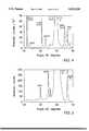
- FIG. 2is a representative x-ray diffraction pattern of a highly ferroelectric heterostructure obtained from growth upon a substrate of Si/SiO 2 according to the present invention
- FIG. 3is a representative x-ray diffraction pattern of a weakly ferroelectric heterostructure resulting from growth upon a substrate lacking a SiO 2 layer;
- FIG. 4is a representative x-ray diffraction pattern of a highly ferroelectric heterostructure obtained from growth upon a LSCO electrode underlayer
- PIG. 5is a representative x-ray diffraction pattern of a weakly ferroelectric heterostructure obtained from growth without a LSCO electrode underlayer;
- FIG. 6is a graph of comparative hysteresis loops obtained from testing heterostructures characterized in FIGS. 2 and 3;
- FIG. 7is a graph of comparative hysteresis loops obtained from testing heterostructures characterized in FIGS. 4 and 5.
- FIG. 1A typical ferroelectric heterostructure memory element 10 prepared according to the present invention is shown in FIG. 1 comprising as a substrate a single crystal oriented [001] silicon wafer 11 the surface of which has been thermally wet-oxidized to form an electronic grade amorphous SiO 2 layer 12 of about 100 nm thickness.
- Another silicon-coating layer material particularly useful in piezoelectric devicesis silicon nitride, Si 3 N 4 .
- PLDpulsed laser deposition
- an excimer laser(248 nm
- a 50-150 nm layer of platinum metalwas then likewise grown on Ti layer 13.
- Other common growth techniquessuch as sputtering, chemical vapor deposition (CVD),
- the PLD apparatuswas used to sequentially deposit the electrode and ferroelectric layers.
- a first electrode layer 15 of LSCOtypically a composition of L 1-x Sr x CoO 3 where x is about 0.15 to 0.85, preferably about 0.5, was grown on the Pt layer 14 to a thickness of about 50-150 nm, preferably about 100 nm.
- Other known metal oxide electrode materialssuch as RuO x , SrRuO 3 , and LaSrCrO 3 , would be equally viable.
- a ferroelectric layer 16 of PLZTfollowed at about 100-500 nm, typically 300 nm.
- the composition of the PLZT materialwas Pb 0 .9 La 0 .1 Zr 0 .2 Ti 0 .8 O 3 in this example, but could be varied over a wide range depending on the intended application. Also, 1% to 10% lanthanum or niobium doping, preferably about 4% to 6%, is useful in optimizing the ferroelectric properties.
- ferroelectric, or paraelectric, materialssuch as barium titanate, barium strontium titanate, lead titanate, bismuth titanate, bismuth strontium tantalate, bismuth strontium niobate, and potassium tantalate niobate, could similarly be employed for layer 16 in high dielectric constant capacitor applications and in pyroelectric and piezoelectric devices.
- a top electrode layer 17 of about 100 nm LSCOwas then grown and the completed heterostructure was cooled to ambient temperature at an optimum rate of about 5°-20° C./min in an atmosphere having an oxygen partial pressure ranging from about 1 ⁇ 10 2 to about 1 ⁇ 10 5 Pa.
- X-ray diffraction examination of the completed polycrystalline heterostructureconfirmed that the ferroelectric stack was fully in the perovskite phase.
- test capacitor electrodes 18were fashioned of the upper LSCO layer 17 upon which Pt/Au electrical contacts 19 were deposited. Complementary contact with bottom electrode layer 15 was established by capacitive coupling through a large conductive pad, not shown, elsewhere on the surface of the structure.
- Typical ferroelectric testing of the capacitor heterostructureshowed very desirable fatigue, aging, and retention properties which were eminently suitable for long term, non-volatile memory application. Remnant polarization values of about 15-20 ⁇ C/cm 2 at 5 V exhibited by the device are quite sufficient for this purpose. Additional testing at more extreme conditions of elevated temperature and the presence of dc bias showed equally satisfactory results. At about 100° C., for example, the device showed good read-write endurance over at least 10 11 cycles.
- Additional heterostructureswere grown to provide samples for testing the efficacy of the processing of the present invention.
- a first heterostructurewas prepared as described above to include SiO 2 layer 12 while in a second sample the SiO 2 layer was omitted.
- Respective x-ray diffraction patterns of the samples depicted in FIGS. 2 and 3show the preferential ferroelectric orientation of the PLZT layers (FIG. 2) grown with SiO 2 interlayer 12 and the weak orientation and diffraction peaks of impurity phases (FIG. 3) resulting from lack of the SiO 2 layer. The respective intensities of the patterns are particularly remarkable.
- Comparative x-ray diffraction patterns of FIGS. 4 and 5were obtained from a second set of samples which differed, respectively, in the inclusion and omission of LSCO layer 15 needed to form the hybrid metal/metal oxide electrode with Pt layer 14 beneath PLZT ferroelectric layer 16 of the heterostructure stack (FIG. 1).
- the effect of the LSCO electrode layer 15can be seen most dramatically in the x-ray diffraction peaks of the PLZT ferroelectric perovskite phase (FIG. 4), as well as in the intensity of the diffractions.
- Without the LSCO electrode layeronly the non-ferroelectric pyrochlore phase (pyro) of the PLZT was formed (FIG. 5).
- ferroelectric properties measurementshighlighted the significant contribution of the SiO 2 layer residing upon the Si wafer substrate, as may be observed in the comparative hysteresis loops of those samples (FIG. 6). Such measurements also confirmed the distinct advantage that the LSCO electrode layer provides for both surface characteristics enabling preferential nucleation of the ferroelectric perovskite phase and superior ferroelectric reliability characteristics.
- the comparative hysteresis loops (FIG. 7) of heterostructures fabricated with and without the LSCO electrode layerillustrate the substantial absence of ferroelectric properties in the latter sample.
- ferroelectric heterostructure capacitor materials of the present inventionhave application for a wide range of devices, such as dielectrics for DRAM capacitors, ferroelectric FET elements for non-destructive readout memories, and electro-optic perovskites grown on SiO 2 /Si substrates for integrated optics, pyroelectric detectors, and the like.
- dielectrics for DRAM capacitorsferroelectric FET elements for non-destructive readout memories
- electro-optic perovskitesgrown on SiO 2 /Si substrates for integrated optics, pyroelectric detectors, and the like.
- FRAMsnonvolatile memory storage media
- MRAMmagnetoresistive random access memories
- magnetic recording anti sensing elementsmay be realized through the integration of ferromagnetic elements and transistor circuitry enabled by the present invention.
- Such structuresare also of particular value for use in integrated microelectromechanical systems in which piezoelectric properties of the ferroelectric materials are utilized.
Landscapes
- Semiconductor Integrated Circuits (AREA)
- Semiconductor Memories (AREA)
- Fixed Capacitors And Capacitor Manufacturing Machines (AREA)
Abstract
Description
Claims (13)
Priority Applications (13)
| Application Number | Priority Date | Filing Date | Title |
|---|---|---|---|
| US08/341,728US5519235A (en) | 1994-11-18 | 1994-11-18 | Polycrystalline ferroelectric capacitor heterostructure employing hybrid electrodes |
| NZ296461ANZ296461A (en) | 1994-11-18 | 1995-11-03 | Ferroelectric capacitor heterostructure on cmos-compatible silicon substrate |
| EP95939139AEP0792524B1 (en) | 1994-11-18 | 1995-11-03 | Polycrystalline ferroelectric capacitor heterostructure employing hybrid electrodes |
| KR1019970703288AKR100296236B1 (en) | 1994-11-18 | 1995-11-03 | Polycrystalline ferroelectric capacitor heterostructure employing hybrid electrodes |
| DE69527642TDE69527642T2 (en) | 1994-11-18 | 1995-11-03 | POLYCRYSTALLINE FERROELECTRIC CAPACITOR HETEROSTRUCTURE WITH HYBRID ELECTRODES |
| PCT/US1995/014740WO1996016447A1 (en) | 1994-11-18 | 1995-11-03 | Polycrystalline ferroelectric capacitor heterostructure employing hybrid electrodes |
| CA 2203524CA2203524C (en) | 1994-11-18 | 1995-11-03 | Polycrystalline ferroelectric capacitor heterostructure employing hybrid electrodes |
| JP8516946AJP3040483B2 (en) | 1994-11-18 | 1995-11-03 | Polycrystalline ferroelectric capacitor heterostructure using hybrid electrode |
| AU41083/96AAU684407B2 (en) | 1994-11-18 | 1995-11-03 | Polycrystalline ferroelectric capacitor heterostructure employing hybrid electrodes |
| MX9703547AMX9703547A (en) | 1994-11-18 | 1995-11-03 | Polycrystalline ferroelectric capacitor heterostructure employing hybrid electrodes. |
| IL11589395AIL115893A (en) | 1994-11-18 | 1995-11-06 | Ferroelectric capacitor structures and their preparation |
| MYPI95003518AMY117284A (en) | 1994-11-18 | 1995-11-18 | Polycrystalline ferroelectric capacitor heterostructure employing hybrid electrodes |
| TW084112387ATW283234B (en) | 1994-11-18 | 1995-11-20 |
Applications Claiming Priority (1)
| Application Number | Priority Date | Filing Date | Title |
|---|---|---|---|
| US08/341,728US5519235A (en) | 1994-11-18 | 1994-11-18 | Polycrystalline ferroelectric capacitor heterostructure employing hybrid electrodes |
Publications (1)
| Publication Number | Publication Date |
|---|---|
| US5519235Atrue US5519235A (en) | 1996-05-21 |
Family
ID=23338770
Family Applications (1)
| Application Number | Title | Priority Date | Filing Date |
|---|---|---|---|
| US08/341,728Expired - Fee RelatedUS5519235A (en) | 1994-11-18 | 1994-11-18 | Polycrystalline ferroelectric capacitor heterostructure employing hybrid electrodes |
Country Status (12)
| Country | Link |
|---|---|
| US (1) | US5519235A (en) |
| EP (1) | EP0792524B1 (en) |
| JP (1) | JP3040483B2 (en) |
| KR (1) | KR100296236B1 (en) |
| AU (1) | AU684407B2 (en) |
| DE (1) | DE69527642T2 (en) |
| IL (1) | IL115893A (en) |
| MX (1) | MX9703547A (en) |
| MY (1) | MY117284A (en) |
| NZ (1) | NZ296461A (en) |
| TW (1) | TW283234B (en) |
| WO (1) | WO1996016447A1 (en) |
Cited By (74)
| Publication number | Priority date | Publication date | Assignee | Title |
|---|---|---|---|---|
| US5593914A (en)* | 1996-03-19 | 1997-01-14 | Radiant Technologies, Inc. | Method for constructing ferroelectric capacitor-like structures on silicon dioxide surfaces |
| US5672903A (en)* | 1995-02-01 | 1997-09-30 | Southern Methodist University | Uncooled ybacuo thin film infrared detector |
| KR19980014897A (en)* | 1996-08-17 | 1998-05-25 | 구자홍 | Capacitor and method of manufacturing the same |
| US5798903A (en)* | 1995-12-26 | 1998-08-25 | Bell Communications Research, Inc. | Electrode structure for ferroelectric capacitor integrated on silicon |
| US5838035A (en)* | 1995-06-28 | 1998-11-17 | Bell Communications Research, Inc. | Barrier layer for ferroelectric capacitor integrated on silicon |
| US5850098A (en)* | 1995-02-01 | 1998-12-15 | Research Corporation Technologies, Inc. | Uncooled amorphous YBaCuO thin film infrared detector |
| WO1998057380A1 (en)* | 1997-06-09 | 1998-12-17 | Bell Communications Research, Inc. | Annealing of a crystalline perovskite ferroelectric cell and cells exhibiting improved barrier properties |
| US5879956A (en)* | 1995-12-27 | 1999-03-09 | Lg Semicon Co., Ltd. | Method of forming a perovskite structure semiconductor capacitor |
| WO1999025014A1 (en)* | 1997-11-10 | 1999-05-20 | Hitachi, Ltd. | Dielectric element and manufacturing method therefor |
| US6048737A (en)* | 1994-09-30 | 2000-04-11 | Samsung Electronics Co., Ltd. | Method for fabricating a ferroelectric capacitor |
| US6071787A (en)* | 1998-03-05 | 2000-06-06 | Lg Semicon Co., Ltd. | Method of forming a capacitor including forming a first and second conductive layers and etching layers to form alloyed conductive sidewall spacers |
| US6128178A (en)* | 1998-07-20 | 2000-10-03 | International Business Machines Corporation | Very thin film capacitor for dynamic random access memory (DRAM) |
| US6146963A (en)* | 1997-12-27 | 2000-11-14 | Hyundai Electronics Industries Co., Ltd. | Methods for forming ferroelectric capacitors having a bottom electrode with decreased leakage current |
| US6163043A (en)* | 1996-04-19 | 2000-12-19 | Matsushita Electronics Corp. | Semiconductor device |
| US6194754B1 (en)* | 1999-03-05 | 2001-02-27 | Telcordia Technologies, Inc. | Amorphous barrier layer in a ferroelectric memory cell |
| US6207082B1 (en)* | 1996-07-24 | 2001-03-27 | Sony Corporation | Layer-structured oxide and process of producing the same |
| US6312819B1 (en) | 1999-05-26 | 2001-11-06 | The Regents Of The University Of California | Oriented conductive oxide electrodes on SiO2/Si and glass |
| US6489644B1 (en)* | 1997-12-26 | 2002-12-03 | Lg Semicon Co., Ltd. | Semiconductor memory device and method for fabricating the same |
| US6501973B1 (en) | 2000-06-30 | 2002-12-31 | Motorola, Inc. | Apparatus and method for measuring selected physical condition of an animate subject |
| US6531740B2 (en) | 2001-07-17 | 2003-03-11 | Motorola, Inc. | Integrated impedance matching and stability network |
| US6555946B1 (en) | 2000-07-24 | 2003-04-29 | Motorola, Inc. | Acoustic wave device and process for forming the same |
| US6589856B2 (en) | 2001-08-06 | 2003-07-08 | Motorola, Inc. | Method and apparatus for controlling anti-phase domains in semiconductor structures and devices |
| US6590236B1 (en) | 2000-07-24 | 2003-07-08 | Motorola, Inc. | Semiconductor structure for use with high-frequency signals |
| WO2003010795A3 (en)* | 2001-07-23 | 2003-08-28 | Motorola Inc | Optical communication device within a semiconductor structure |
| US20030183859A1 (en)* | 2000-08-24 | 2003-10-02 | Gnadinger Fred P. | Single transistor rare earth manganite ferroelectric nonvolatile memory cell |
| US6638838B1 (en) | 2000-10-02 | 2003-10-28 | Motorola, Inc. | Semiconductor structure including a partially annealed layer and method of forming the same |
| US6639249B2 (en) | 2001-08-06 | 2003-10-28 | Motorola, Inc. | Structure and method for fabrication for a solid-state lighting device |
| US6646293B2 (en) | 2001-07-18 | 2003-11-11 | Motorola, Inc. | Structure for fabricating high electron mobility transistors utilizing the formation of complaint substrates |
| US6667196B2 (en) | 2001-07-25 | 2003-12-23 | Motorola, Inc. | Method for real-time monitoring and controlling perovskite oxide film growth and semiconductor structure formed using the method |
| US6674110B2 (en) | 2001-03-02 | 2004-01-06 | Cova Technologies, Inc. | Single transistor ferroelectric memory cell, device and method for the formation of the same incorporating a high temperature ferroelectric gate dielectric |
| US6673646B2 (en) | 2001-02-28 | 2004-01-06 | Motorola, Inc. | Growth of compound semiconductor structures on patterned oxide films and process for fabricating same |
| US6673667B2 (en) | 2001-08-15 | 2004-01-06 | Motorola, Inc. | Method for manufacturing a substantially integral monolithic apparatus including a plurality of semiconductor materials |
| US6693033B2 (en) | 2000-02-10 | 2004-02-17 | Motorola, Inc. | Method of removing an amorphous oxide from a monocrystalline surface |
| US6693298B2 (en) | 2001-07-20 | 2004-02-17 | Motorola, Inc. | Structure and method for fabricating epitaxial semiconductor on insulator (SOI) structures and devices utilizing the formation of a compliant substrate for materials used to form same |
| US20040041186A1 (en)* | 2002-08-28 | 2004-03-04 | Klaus Dimmler | Ferroelectric transistor with enhanced data retention |
| US6709989B2 (en) | 2001-06-21 | 2004-03-23 | Motorola, Inc. | Method for fabricating a semiconductor structure including a metal oxide interface with silicon |
| US6714435B1 (en) | 2002-09-19 | 2004-03-30 | Cova Technologies, Inc. | Ferroelectric transistor for storing two data bits |
| US20040065912A1 (en)* | 2002-10-08 | 2004-04-08 | Shangqing Liu | Electrically programmable nonvolatile variable capacitor |
| US20040066116A1 (en)* | 2002-08-08 | 2004-04-08 | Canon Kabushiki Kaisha | Actuator and liquid discharge head, and method for manufacturing liquid discharge head |
| US6855992B2 (en) | 2001-07-24 | 2005-02-15 | Motorola Inc. | Structure and method for fabricating configurable transistor devices utilizing the formation of a compliant substrate for materials used to form the same |
| US6885065B2 (en) | 2002-11-20 | 2005-04-26 | Freescale Semiconductor, Inc. | Ferromagnetic semiconductor structure and method for forming the same |
| US6888736B2 (en) | 2002-09-19 | 2005-05-03 | Cova Technologies, Inc. | Ferroelectric transistor for storing two data bits |
| US20050095389A1 (en)* | 2003-10-31 | 2005-05-05 | International Business Machines Corporation | Method and structure for ultra-high density, high data rate ferroelectric storage disk technology using stabilization by a surface conducting layer |
| US6916717B2 (en) | 2002-05-03 | 2005-07-12 | Motorola, Inc. | Method for growing a monocrystalline oxide layer and for fabricating a semiconductor device on a monocrystalline substrate |
| US6965128B2 (en) | 2003-02-03 | 2005-11-15 | Freescale Semiconductor, Inc. | Structure and method for fabricating semiconductor microresonator devices |
| US20050285171A1 (en)* | 2004-06-11 | 2005-12-29 | Tai-Bor Wu | Ferroelectric material and ferroelectric memory device made therefrom |
| US6992321B2 (en) | 2001-07-13 | 2006-01-31 | Motorola, Inc. | Structure and method for fabricating semiconductor structures and devices utilizing piezoelectric materials |
| US7005717B2 (en) | 2000-05-31 | 2006-02-28 | Freescale Semiconductor, Inc. | Semiconductor device and method |
| US7020374B2 (en) | 2003-02-03 | 2006-03-28 | Freescale Semiconductor, Inc. | Optical waveguide structure and method for fabricating the same |
| US7019332B2 (en) | 2001-07-20 | 2006-03-28 | Freescale Semiconductor, Inc. | Fabrication of a wavelength locker within a semiconductor structure |
| US7045815B2 (en) | 2001-04-02 | 2006-05-16 | Freescale Semiconductor, Inc. | Semiconductor structure exhibiting reduced leakage current and method of fabricating same |
| US20060124470A1 (en)* | 2002-11-05 | 2006-06-15 | Tetsuji Zama | Conductive polymer composite structure |
| US7067856B2 (en) | 2000-02-10 | 2006-06-27 | Freescale Semiconductor, Inc. | Semiconductor structure, semiconductor device, communicating device, integrated circuit, and process for fabricating the same |
| US7105866B2 (en) | 2000-07-24 | 2006-09-12 | Freescale Semiconductor, Inc. | Heterojunction tunneling diodes and process for fabricating same |
| US7161227B2 (en) | 2001-08-14 | 2007-01-09 | Motorola, Inc. | Structure and method for fabricating semiconductor structures and devices for detecting an object |
| US7169619B2 (en) | 2002-11-19 | 2007-01-30 | Freescale Semiconductor, Inc. | Method for fabricating semiconductor structures on vicinal substrates using a low temperature, low pressure, alkaline earth metal-rich process |
| US7211852B2 (en) | 2001-01-19 | 2007-05-01 | Freescale Semiconductor, Inc. | Structure and method for fabricating GaN devices utilizing the formation of a compliant substrate |
| US7342276B2 (en) | 2001-10-17 | 2008-03-11 | Freescale Semiconductor, Inc. | Method and apparatus utilizing monocrystalline insulator |
| US20100291378A1 (en)* | 2006-12-01 | 2010-11-18 | The Trustees Of The University Of Pennsylvania | Ferroelectric ultrathin perovskite films |
| US20120221086A1 (en)* | 2009-10-30 | 2012-08-30 | St. Jude Medical Ab | Mri-compatible implantable medical lead |
| WO2012166562A1 (en)* | 2011-05-27 | 2012-12-06 | University Of North Texas | Graphene magnetic tunnel junction spin filters and methods of making |
| WO2016160917A1 (en)* | 2015-03-30 | 2016-10-06 | Massachusetts Institute Of Technology | Segregation resistant perovskite oxides with surface modification |
| US10199682B2 (en) | 2011-06-29 | 2019-02-05 | Space Charge, LLC | Rugged, gel-free, lithium-free, high energy density solid-state electrochemical energy storage devices |
| US10601074B2 (en) | 2011-06-29 | 2020-03-24 | Space Charge, LLC | Rugged, gel-free, lithium-free, high energy density solid-state electrochemical energy storage devices |
| US10658705B2 (en) | 2018-03-07 | 2020-05-19 | Space Charge, LLC | Thin-film solid-state energy storage devices |
| US11164976B2 (en) | 2019-04-08 | 2021-11-02 | Kepler Computing Inc. | Doped polar layers and semiconductor device incorporating same |
| US11289497B2 (en) | 2019-12-27 | 2022-03-29 | Kepler Computing Inc. | Integration method of ferroelectric memory array |
| US11430861B2 (en) | 2019-12-27 | 2022-08-30 | Kepler Computing Inc. | Ferroelectric capacitor and method of patterning such |
| US11482528B2 (en) | 2019-12-27 | 2022-10-25 | Kepler Computing Inc. | Pillar capacitor and method of fabricating such |
| US11501905B2 (en)* | 2020-08-31 | 2022-11-15 | Boston Applied Technologies, Inc. | Composition and method of making a monolithic heterostructure of multiferroic thin films |
| US11527774B2 (en) | 2011-06-29 | 2022-12-13 | Space Charge, LLC | Electrochemical energy storage devices |
| US11765909B1 (en) | 2021-06-11 | 2023-09-19 | Kepler Computing Inc. | Process integration flow for embedded memory enabled by decoupling processing of a memory area from a non-memory area |
| CN117548095A (en)* | 2023-11-24 | 2024-02-13 | 扬州大学 | Preparation method and application of bismuth titanate B-site niobium element doped photo/piezoelectric catalytic material |
| US11996517B2 (en) | 2011-06-29 | 2024-05-28 | Space Charge, LLC | Electrochemical energy storage devices |
Families Citing this family (3)
| Publication number | Priority date | Publication date | Assignee | Title |
|---|---|---|---|---|
| US5807774A (en) | 1996-12-06 | 1998-09-15 | Sharp Kabushiki Kaisha | Simple method of fabricating ferroelectric capacitors |
| JP3169866B2 (en) | 1997-11-04 | 2001-05-28 | 日本電気株式会社 | Thin film capacitor and method of manufacturing the same |
| EP1770778B1 (en)* | 2004-07-22 | 2012-03-14 | Nippon Telegraph And Telephone Corporation | Apparatus for obtaining double stable resistance values, method for manufacturing the same, metal oxide thin film and method for manufacturing the same |
Citations (4)
| Publication number | Priority date | Publication date | Assignee | Title |
|---|---|---|---|---|
| US5155658A (en)* | 1992-03-05 | 1992-10-13 | Bell Communications Research, Inc. | Crystallographically aligned ferroelectric films usable in memories and method of crystallographically aligning perovskite films |
| US5248564A (en)* | 1992-12-09 | 1993-09-28 | Bell Communications Research, Inc. | C-axis perovskite thin films grown on silicon dioxide |
| US5270298A (en)* | 1992-03-05 | 1993-12-14 | Bell Communications Research, Inc. | Cubic metal oxide thin film epitaxially grown on silicon |
| US5387459A (en)* | 1992-12-17 | 1995-02-07 | Eastman Kodak Company | Multilayer structure having an epitaxial metal electrode |
Family Cites Families (3)
| Publication number | Priority date | Publication date | Assignee | Title |
|---|---|---|---|---|
| NL9000602A (en)* | 1990-03-16 | 1991-10-16 | Philips Nv | METHOD FOR MANUFACTURING A SEMICONDUCTOR DEVICE WITH MEMORY ELEMENTS FORMING CAPACITORS WITH A FERROELECTRIC DIELECTRIC. |
| JP3006053B2 (en)* | 1990-08-07 | 2000-02-07 | セイコーエプソン株式会社 | Semiconductor device |
| TW200600B (en)* | 1991-10-01 | 1993-02-21 | Philips Nv |
- 1994
- 1994-11-18USUS08/341,728patent/US5519235A/ennot_activeExpired - Fee Related
- 1995
- 1995-11-03AUAU41083/96Apatent/AU684407B2/ennot_activeCeased
- 1995-11-03MXMX9703547Apatent/MX9703547A/ennot_activeIP Right Cessation
- 1995-11-03EPEP95939139Apatent/EP0792524B1/ennot_activeExpired - Lifetime
- 1995-11-03NZNZ296461Apatent/NZ296461A/enunknown
- 1995-11-03WOPCT/US1995/014740patent/WO1996016447A1/enactiveIP Right Grant
- 1995-11-03DEDE69527642Tpatent/DE69527642T2/ennot_activeExpired - Fee Related
- 1995-11-03KRKR1019970703288Apatent/KR100296236B1/ennot_activeExpired - Fee Related
- 1995-11-03JPJP8516946Apatent/JP3040483B2/ennot_activeExpired - Lifetime
- 1995-11-06ILIL11589395Apatent/IL115893A/enactiveIP Right Grant
- 1995-11-18MYMYPI95003518Apatent/MY117284A/enunknown
- 1995-11-20TWTW084112387Apatent/TW283234B/zhactive
Patent Citations (4)
| Publication number | Priority date | Publication date | Assignee | Title |
|---|---|---|---|---|
| US5155658A (en)* | 1992-03-05 | 1992-10-13 | Bell Communications Research, Inc. | Crystallographically aligned ferroelectric films usable in memories and method of crystallographically aligning perovskite films |
| US5270298A (en)* | 1992-03-05 | 1993-12-14 | Bell Communications Research, Inc. | Cubic metal oxide thin film epitaxially grown on silicon |
| US5248564A (en)* | 1992-12-09 | 1993-09-28 | Bell Communications Research, Inc. | C-axis perovskite thin films grown on silicon dioxide |
| US5387459A (en)* | 1992-12-17 | 1995-02-07 | Eastman Kodak Company | Multilayer structure having an epitaxial metal electrode |
Cited By (126)
| Publication number | Priority date | Publication date | Assignee | Title |
|---|---|---|---|---|
| US6048737A (en)* | 1994-09-30 | 2000-04-11 | Samsung Electronics Co., Ltd. | Method for fabricating a ferroelectric capacitor |
| US5672903A (en)* | 1995-02-01 | 1997-09-30 | Southern Methodist University | Uncooled ybacuo thin film infrared detector |
| US5850098A (en)* | 1995-02-01 | 1998-12-15 | Research Corporation Technologies, Inc. | Uncooled amorphous YBaCuO thin film infrared detector |
| US5838035A (en)* | 1995-06-28 | 1998-11-17 | Bell Communications Research, Inc. | Barrier layer for ferroelectric capacitor integrated on silicon |
| US5798903A (en)* | 1995-12-26 | 1998-08-25 | Bell Communications Research, Inc. | Electrode structure for ferroelectric capacitor integrated on silicon |
| US6194753B1 (en) | 1995-12-27 | 2001-02-27 | Hyundai Electronics Industries Co., Ltd. | Method of forming a perovskite structure semiconductor capacitor |
| US5879956A (en)* | 1995-12-27 | 1999-03-09 | Lg Semicon Co., Ltd. | Method of forming a perovskite structure semiconductor capacitor |
| WO1997035339A1 (en)* | 1996-03-19 | 1997-09-25 | Radiant Technologies, Inc. | Method for constructing ferroelectric capacitor-like structures on silicon dioxide surfaces |
| US5593914A (en)* | 1996-03-19 | 1997-01-14 | Radiant Technologies, Inc. | Method for constructing ferroelectric capacitor-like structures on silicon dioxide surfaces |
| US6420743B1 (en) | 1996-04-19 | 2002-07-16 | Matsushita Electronics, Corp. | Semiconductor device |
| US6163043A (en)* | 1996-04-19 | 2000-12-19 | Matsushita Electronics Corp. | Semiconductor device |
| US6207082B1 (en)* | 1996-07-24 | 2001-03-27 | Sony Corporation | Layer-structured oxide and process of producing the same |
| KR19980014897A (en)* | 1996-08-17 | 1998-05-25 | 구자홍 | Capacitor and method of manufacturing the same |
| WO1998057380A1 (en)* | 1997-06-09 | 1998-12-17 | Bell Communications Research, Inc. | Annealing of a crystalline perovskite ferroelectric cell and cells exhibiting improved barrier properties |
| US6274388B1 (en) | 1997-06-09 | 2001-08-14 | Telcordia Technologies, Inc. | Annealing of a crystalline perovskite ferroelectric cell |
| WO1999025014A1 (en)* | 1997-11-10 | 1999-05-20 | Hitachi, Ltd. | Dielectric element and manufacturing method therefor |
| US6489644B1 (en)* | 1997-12-26 | 2002-12-03 | Lg Semicon Co., Ltd. | Semiconductor memory device and method for fabricating the same |
| US6146963A (en)* | 1997-12-27 | 2000-11-14 | Hyundai Electronics Industries Co., Ltd. | Methods for forming ferroelectric capacitors having a bottom electrode with decreased leakage current |
| US6071787A (en)* | 1998-03-05 | 2000-06-06 | Lg Semicon Co., Ltd. | Method of forming a capacitor including forming a first and second conductive layers and etching layers to form alloyed conductive sidewall spacers |
| US6128178A (en)* | 1998-07-20 | 2000-10-03 | International Business Machines Corporation | Very thin film capacitor for dynamic random access memory (DRAM) |
| US6194754B1 (en)* | 1999-03-05 | 2001-02-27 | Telcordia Technologies, Inc. | Amorphous barrier layer in a ferroelectric memory cell |
| US6610549B1 (en)* | 1999-03-05 | 2003-08-26 | University Of Maryland, College Park | Amorphous barrier layer in a ferroelectric memory cell |
| US6312819B1 (en) | 1999-05-26 | 2001-11-06 | The Regents Of The University Of California | Oriented conductive oxide electrodes on SiO2/Si and glass |
| US6743292B2 (en) | 1999-05-26 | 2004-06-01 | The Regents Of The University Of California | Oriented conductive oxide electrodes on SiO2/Si and glass |
| US6693033B2 (en) | 2000-02-10 | 2004-02-17 | Motorola, Inc. | Method of removing an amorphous oxide from a monocrystalline surface |
| US7067856B2 (en) | 2000-02-10 | 2006-06-27 | Freescale Semiconductor, Inc. | Semiconductor structure, semiconductor device, communicating device, integrated circuit, and process for fabricating the same |
| US7005717B2 (en) | 2000-05-31 | 2006-02-28 | Freescale Semiconductor, Inc. | Semiconductor device and method |
| US6501973B1 (en) | 2000-06-30 | 2002-12-31 | Motorola, Inc. | Apparatus and method for measuring selected physical condition of an animate subject |
| US6590236B1 (en) | 2000-07-24 | 2003-07-08 | Motorola, Inc. | Semiconductor structure for use with high-frequency signals |
| US6555946B1 (en) | 2000-07-24 | 2003-04-29 | Motorola, Inc. | Acoustic wave device and process for forming the same |
| US7105866B2 (en) | 2000-07-24 | 2006-09-12 | Freescale Semiconductor, Inc. | Heterojunction tunneling diodes and process for fabricating same |
| US20030183859A1 (en)* | 2000-08-24 | 2003-10-02 | Gnadinger Fred P. | Single transistor rare earth manganite ferroelectric nonvolatile memory cell |
| US7030435B2 (en) | 2000-08-24 | 2006-04-18 | Cova Technologies, Inc. | Single transistor rare earth manganite ferroelectric nonvolatile memory cell |
| US6638838B1 (en) | 2000-10-02 | 2003-10-28 | Motorola, Inc. | Semiconductor structure including a partially annealed layer and method of forming the same |
| US7211852B2 (en) | 2001-01-19 | 2007-05-01 | Freescale Semiconductor, Inc. | Structure and method for fabricating GaN devices utilizing the formation of a compliant substrate |
| US6673646B2 (en) | 2001-02-28 | 2004-01-06 | Motorola, Inc. | Growth of compound semiconductor structures on patterned oxide films and process for fabricating same |
| US6674110B2 (en) | 2001-03-02 | 2004-01-06 | Cova Technologies, Inc. | Single transistor ferroelectric memory cell, device and method for the formation of the same incorporating a high temperature ferroelectric gate dielectric |
| US7045815B2 (en) | 2001-04-02 | 2006-05-16 | Freescale Semiconductor, Inc. | Semiconductor structure exhibiting reduced leakage current and method of fabricating same |
| US6709989B2 (en) | 2001-06-21 | 2004-03-23 | Motorola, Inc. | Method for fabricating a semiconductor structure including a metal oxide interface with silicon |
| US6992321B2 (en) | 2001-07-13 | 2006-01-31 | Motorola, Inc. | Structure and method for fabricating semiconductor structures and devices utilizing piezoelectric materials |
| US6531740B2 (en) | 2001-07-17 | 2003-03-11 | Motorola, Inc. | Integrated impedance matching and stability network |
| US6646293B2 (en) | 2001-07-18 | 2003-11-11 | Motorola, Inc. | Structure for fabricating high electron mobility transistors utilizing the formation of complaint substrates |
| US6693298B2 (en) | 2001-07-20 | 2004-02-17 | Motorola, Inc. | Structure and method for fabricating epitaxial semiconductor on insulator (SOI) structures and devices utilizing the formation of a compliant substrate for materials used to form same |
| US7019332B2 (en) | 2001-07-20 | 2006-03-28 | Freescale Semiconductor, Inc. | Fabrication of a wavelength locker within a semiconductor structure |
| WO2003010795A3 (en)* | 2001-07-23 | 2003-08-28 | Motorola Inc | Optical communication device within a semiconductor structure |
| US6855992B2 (en) | 2001-07-24 | 2005-02-15 | Motorola Inc. | Structure and method for fabricating configurable transistor devices utilizing the formation of a compliant substrate for materials used to form the same |
| US6667196B2 (en) | 2001-07-25 | 2003-12-23 | Motorola, Inc. | Method for real-time monitoring and controlling perovskite oxide film growth and semiconductor structure formed using the method |
| US6589856B2 (en) | 2001-08-06 | 2003-07-08 | Motorola, Inc. | Method and apparatus for controlling anti-phase domains in semiconductor structures and devices |
| US6639249B2 (en) | 2001-08-06 | 2003-10-28 | Motorola, Inc. | Structure and method for fabrication for a solid-state lighting device |
| US7161227B2 (en) | 2001-08-14 | 2007-01-09 | Motorola, Inc. | Structure and method for fabricating semiconductor structures and devices for detecting an object |
| US6673667B2 (en) | 2001-08-15 | 2004-01-06 | Motorola, Inc. | Method for manufacturing a substantially integral monolithic apparatus including a plurality of semiconductor materials |
| US7342276B2 (en) | 2001-10-17 | 2008-03-11 | Freescale Semiconductor, Inc. | Method and apparatus utilizing monocrystalline insulator |
| US6916717B2 (en) | 2002-05-03 | 2005-07-12 | Motorola, Inc. | Method for growing a monocrystalline oxide layer and for fabricating a semiconductor device on a monocrystalline substrate |
| US7045935B2 (en)* | 2002-08-08 | 2006-05-16 | Canon Kabushiki Kaisha | Actuator and liquid discharge head, and method for manufacturing liquid discharge head |
| US20040066116A1 (en)* | 2002-08-08 | 2004-04-08 | Canon Kabushiki Kaisha | Actuator and liquid discharge head, and method for manufacturing liquid discharge head |
| US20040041186A1 (en)* | 2002-08-28 | 2004-03-04 | Klaus Dimmler | Ferroelectric transistor with enhanced data retention |
| US6825517B2 (en) | 2002-08-28 | 2004-11-30 | Cova Technologies, Inc. | Ferroelectric transistor with enhanced data retention |
| US6790679B2 (en) | 2002-08-28 | 2004-09-14 | Cova Technologies, Inc. | Ferroelectric transistor with enhanced data retention |
| US6714435B1 (en) | 2002-09-19 | 2004-03-30 | Cova Technologies, Inc. | Ferroelectric transistor for storing two data bits |
| US6888736B2 (en) | 2002-09-19 | 2005-05-03 | Cova Technologies, Inc. | Ferroelectric transistor for storing two data bits |
| US7034349B2 (en) | 2002-09-19 | 2006-04-25 | Cova Technologies, Inc. | Ferroelectric transistor for storing two data bits |
| US20040141357A1 (en)* | 2002-09-19 | 2004-07-22 | Klaus Dimmler | Ferroelectric transistor for storing two data bits |
| US6762481B2 (en)* | 2002-10-08 | 2004-07-13 | The University Of Houston System | Electrically programmable nonvolatile variable capacitor |
| US20040065912A1 (en)* | 2002-10-08 | 2004-04-08 | Shangqing Liu | Electrically programmable nonvolatile variable capacitor |
| US20060124470A1 (en)* | 2002-11-05 | 2006-06-15 | Tetsuji Zama | Conductive polymer composite structure |
| US7169619B2 (en) | 2002-11-19 | 2007-01-30 | Freescale Semiconductor, Inc. | Method for fabricating semiconductor structures on vicinal substrates using a low temperature, low pressure, alkaline earth metal-rich process |
| US6885065B2 (en) | 2002-11-20 | 2005-04-26 | Freescale Semiconductor, Inc. | Ferromagnetic semiconductor structure and method for forming the same |
| US7020374B2 (en) | 2003-02-03 | 2006-03-28 | Freescale Semiconductor, Inc. | Optical waveguide structure and method for fabricating the same |
| US6965128B2 (en) | 2003-02-03 | 2005-11-15 | Freescale Semiconductor, Inc. | Structure and method for fabricating semiconductor microresonator devices |
| US8125823B2 (en) | 2003-10-31 | 2012-02-28 | International Business Machines Corporation | Method and structure for ultra-high density, high data rate ferroelectric storage disk technology using stabilization by a surface conducting layer |
| US20050095389A1 (en)* | 2003-10-31 | 2005-05-05 | International Business Machines Corporation | Method and structure for ultra-high density, high data rate ferroelectric storage disk technology using stabilization by a surface conducting layer |
| US8743586B2 (en) | 2003-10-31 | 2014-06-03 | International Business Machines Corporation | Method and structure for ultra-high density, high data rate ferroelectric storage disk technology using stabilization by a surface conducting layer |
| US20090310472A1 (en)* | 2003-10-31 | 2009-12-17 | International Business Machines Corporation | Method and structure for ultra-high density, high data rate ferroelectric storage disk technology using stabilization by a surface conducting layer |
| US7754353B2 (en)* | 2003-10-31 | 2010-07-13 | Newns Dennis M | Method and structure for ultra-high density, high data rate ferroelectric storage disk technology using stabilization by a surface conducting layer |
| US7307304B2 (en) | 2004-06-11 | 2007-12-11 | National Tsing Hua University | Ferroelectric materials and ferroelectric memory device made therefrom |
| US20050285171A1 (en)* | 2004-06-11 | 2005-12-29 | Tai-Bor Wu | Ferroelectric material and ferroelectric memory device made therefrom |
| US20100291378A1 (en)* | 2006-12-01 | 2010-11-18 | The Trustees Of The University Of Pennsylvania | Ferroelectric ultrathin perovskite films |
| US8603573B2 (en)* | 2006-12-01 | 2013-12-10 | The Trustees Of The University Of Pennsylvania | Ferroelectric ultrathin perovskite films |
| US20120221086A1 (en)* | 2009-10-30 | 2012-08-30 | St. Jude Medical Ab | Mri-compatible implantable medical lead |
| US8805535B2 (en)* | 2009-10-30 | 2014-08-12 | St. Jude Medical Ab | MRI-compatible implantable medical lead |
| WO2012166562A1 (en)* | 2011-05-27 | 2012-12-06 | University Of North Texas | Graphene magnetic tunnel junction spin filters and methods of making |
| US10601074B2 (en) | 2011-06-29 | 2020-03-24 | Space Charge, LLC | Rugged, gel-free, lithium-free, high energy density solid-state electrochemical energy storage devices |
| US10199682B2 (en) | 2011-06-29 | 2019-02-05 | Space Charge, LLC | Rugged, gel-free, lithium-free, high energy density solid-state electrochemical energy storage devices |
| US11996517B2 (en) | 2011-06-29 | 2024-05-28 | Space Charge, LLC | Electrochemical energy storage devices |
| US11527774B2 (en) | 2011-06-29 | 2022-12-13 | Space Charge, LLC | Electrochemical energy storage devices |
| US20180093229A1 (en)* | 2015-03-30 | 2018-04-05 | Massachusetts Institute Of Technology | Segregation resistant perovskite oxides with surface modification |
| WO2016160917A1 (en)* | 2015-03-30 | 2016-10-06 | Massachusetts Institute Of Technology | Segregation resistant perovskite oxides with surface modification |
| US11179682B2 (en)* | 2015-03-30 | 2021-11-23 | Massachusetts Institute Of Technology | Segregation resistant perovskite oxides with surface modification |
| US10658705B2 (en) | 2018-03-07 | 2020-05-19 | Space Charge, LLC | Thin-film solid-state energy storage devices |
| US11296228B2 (en) | 2019-04-08 | 2022-04-05 | Kepler Computing Inc. | Doped polar layers and semiconductor device incorporating same |
| US11949017B2 (en) | 2019-04-08 | 2024-04-02 | Kepler Computing Inc. | Doped polar layers and semiconductor device incorporating same |
| US12369351B2 (en) | 2019-04-08 | 2025-07-22 | Kepler Computing Inc. | Doped polar layers and semiconductor device incorporating same |
| US11349031B2 (en) | 2019-04-08 | 2022-05-31 | Kepler Computing Inc. | Doped polar layers and semiconductor device incorporating same |
| US11355643B2 (en) | 2019-04-08 | 2022-06-07 | Kepler Computing Inc. | Doped polar layers and semiconductor device incorporating same |
| US11398570B2 (en) | 2019-04-08 | 2022-07-26 | Kepler Computing Inc. | Doped polar layers and semiconductor device incorporating same |
| US11411116B2 (en) | 2019-04-08 | 2022-08-09 | Kepler Computing Inc. | Doped polar layers and semiconductor device incorporating same |
| US11417768B2 (en) | 2019-04-08 | 2022-08-16 | Kepler Computing Inc. | Doped polar layers and semiconductor device incorporating same |
| US12294029B2 (en) | 2019-04-08 | 2025-05-06 | Kepler Computing Inc. | Doped polar layers and semiconductor device incorporating same |
| US11444203B2 (en) | 2019-04-08 | 2022-09-13 | Kepler Computing Inc. | Doped polar layers and semiconductor device incorporating same |
| US11469327B2 (en) | 2019-04-08 | 2022-10-11 | Kepler Computing Inc. | Doped polar layers and semiconductor device incorporating same |
| US11164976B2 (en) | 2019-04-08 | 2021-11-02 | Kepler Computing Inc. | Doped polar layers and semiconductor device incorporating same |
| US11949018B2 (en) | 2019-04-08 | 2024-04-02 | Kepler Computing Inc. | Doped polar layers and semiconductor device incorporating same |
| US11289608B2 (en) | 2019-04-08 | 2022-03-29 | Kepler Computing Inc. | Doped polar layers and semiconductor device incorporating same |
| US11289607B2 (en) | 2019-04-08 | 2022-03-29 | Kepler Computing Inc. | Doped polar layers and semiconductor device incorporating same |
| US11916149B2 (en) | 2019-04-08 | 2024-02-27 | Kepler Computing Inc. | Doped polar layers and semiconductor device incorporating same |
| US11757043B2 (en) | 2019-04-08 | 2023-09-12 | Kepler Computing Inc. | Doped polar layers and semiconductor device incorporating same |
| US11908943B2 (en) | 2019-04-08 | 2024-02-20 | Kepler Computing Inc. | Manganese-doped perovskite layers and semiconductor device incorporating same |
| US11888066B2 (en) | 2019-04-08 | 2024-01-30 | Kepler Computing Inc. | Doped polar layers and semiconductor device incorporating same |
| US11888067B2 (en) | 2019-04-08 | 2024-01-30 | Kepler Computing Inc. | B-site doped perovskite layers and semiconductor device incorporating same |
| US11848386B2 (en) | 2019-04-08 | 2023-12-19 | Kepler Computing Inc. | B-site doped perovskite layers and semiconductor device incorporating same |
| US11837664B2 (en) | 2019-04-08 | 2023-12-05 | Kepler Computing Inc. | Doped polar layers and semiconductor device incorporating same |
| US12113097B2 (en) | 2019-12-27 | 2024-10-08 | Kepler Computing Inc. | Ferroelectric capacitor integrated with logic |
| US12137574B2 (en) | 2019-12-27 | 2024-11-05 | Kepler Computing Inc. | Integration of ferroelectric memory devices having stacked electrodes with transistors |
| US11289497B2 (en) | 2019-12-27 | 2022-03-29 | Kepler Computing Inc. | Integration method of ferroelectric memory array |
| US11430861B2 (en) | 2019-12-27 | 2022-08-30 | Kepler Computing Inc. | Ferroelectric capacitor and method of patterning such |
| US11758738B2 (en) | 2019-12-27 | 2023-09-12 | Kepler Computing Inc. | Integration of ferroelectric memory devices with transistors |
| US11641747B2 (en) | 2019-12-27 | 2023-05-02 | Kepler Computing Inc. | Integration of a ferroelectric memory device with a transistor |
| US12200941B2 (en) | 2019-12-27 | 2025-01-14 | Kepler Computing Inc. | Pillar capacitor and method of fabricating such |
| US11482528B2 (en) | 2019-12-27 | 2022-10-25 | Kepler Computing Inc. | Pillar capacitor and method of fabricating such |
| US11522044B2 (en) | 2019-12-27 | 2022-12-06 | Kepler Computing Inc. | Ferroelectric capacitor integrated with logic |
| US11501905B2 (en)* | 2020-08-31 | 2022-11-15 | Boston Applied Technologies, Inc. | Composition and method of making a monolithic heterostructure of multiferroic thin films |
| US11792998B1 (en) | 2021-06-11 | 2023-10-17 | Kepler Computing Inc. | Process integration flow for embedded memory with multi-pocket masks for decoupling processing of memory areas from non-memory areas |
| US11785782B1 (en) | 2021-06-11 | 2023-10-10 | Kepler Computing Inc. | Embedded memory with encapsulation layer adjacent to a memory stack |
| US12238935B1 (en) | 2021-06-11 | 2025-02-25 | Kepler Computing Inc. | Embedded memory adjacent to non-memory |
| US11765909B1 (en) | 2021-06-11 | 2023-09-19 | Kepler Computing Inc. | Process integration flow for embedded memory enabled by decoupling processing of a memory area from a non-memory area |
| CN117548095A (en)* | 2023-11-24 | 2024-02-13 | 扬州大学 | Preparation method and application of bismuth titanate B-site niobium element doped photo/piezoelectric catalytic material |
Also Published As
| Publication number | Publication date |
|---|---|
| JP3040483B2 (en) | 2000-05-15 |
| AU4108396A (en) | 1996-06-17 |
| TW283234B (en) | 1996-08-11 |
| NZ296461A (en) | 1999-03-29 |
| IL115893A0 (en) | 1996-01-31 |
| JPH09512963A (en) | 1997-12-22 |
| IL115893A (en) | 1998-08-16 |
| WO1996016447A1 (en) | 1996-05-30 |
| DE69527642D1 (en) | 2002-09-05 |
| KR970707588A (en) | 1997-12-01 |
| EP0792524A4 (en) | 1999-03-17 |
| MY117284A (en) | 2004-06-30 |
| EP0792524A1 (en) | 1997-09-03 |
| KR100296236B1 (en) | 2001-08-07 |
| AU684407B2 (en) | 1997-12-11 |
| MX9703547A (en) | 1997-08-30 |
| EP0792524B1 (en) | 2002-07-31 |
| DE69527642T2 (en) | 2003-04-03 |
Similar Documents
| Publication | Publication Date | Title |
|---|---|---|
| US5519235A (en) | Polycrystalline ferroelectric capacitor heterostructure employing hybrid electrodes | |
| US5479317A (en) | Ferroelectric capacitor heterostructure and method of making same | |
| MXPA97003547A (en) | Heteroestructura of polycrystalline ferroelectric capacitor that uses hybrid electrodes | |
| US6441417B1 (en) | Single c-axis PGO thin film on ZrO2 for non-volatile memory applications and methods of making the same | |
| EP0747937B1 (en) | Method of forming a substrate coated with a ferroelectric thin film | |
| US5248564A (en) | C-axis perovskite thin films grown on silicon dioxide | |
| EP0732422B1 (en) | Ferroelectric thin-film coated substrate, method for its manufacture and nonvolatile memory comprising such a substrate | |
| US5753934A (en) | Multilayer thin film, substrate for electronic device, electronic device, and preparation of multilayer oxide thin film | |
| KR100228040B1 (en) | Nonvolatile Semiconductor Memory and Manufacturing Method | |
| Liu et al. | Epitaxial La-doped SrTiO 3 on silicon: A conductive template for epitaxial ferroelectrics on silicon | |
| KR100413618B1 (en) | Low imprint ferroelectric material for long retention memory and method of making the same | |
| US6197600B1 (en) | Ferroelectric thin film, manufacturing method thereof and device incorporating the same | |
| JP4772188B2 (en) | Method for making ferroelectric capacitor and method for growing PZT layer on substrate | |
| EP0616726B1 (en) | Layered superlattice material applications | |
| KR20010071697A (en) | Ferroelectric field effect transistor having compositionally graded ferroelectric material and method of making the same | |
| JP2000169297A (en) | Method for producing oxide ferroelectric thin film, oxide ferroelectric thin film, and oxide ferroelectric thin film element | |
| US6307225B1 (en) | Insulating material, substrate covered with an insulating film, method of producing the same, and thin-film device | |
| US20020153543A1 (en) | Method for manufacturing oxide ferroelectric thin film oxide ferroelectric thin film and oxide ferroelectric thin film element | |
| KR19990006318A (en) | Deposition of Ferroelectric Films and Ferroelectric Capacitor Devices | |
| CA2203524C (en) | Polycrystalline ferroelectric capacitor heterostructure employing hybrid electrodes | |
| KR19990072528A (en) | Ferroelectric thin film device and method of producing the same | |
| CN1164295A (en) | Polycrystalline Ferroelectric Capacitor Heterostructure Using Mixed Electrodes | |
| Norga et al. | Growth of (111)-oriented Pb (Zr, Ti) O3 layers on nanocrystalline RuO2 electrodes using the sol-gel technique | |
| JPH0974169A (en) | Thin film capacitors | |
| Stancu et al. | Comparison between PZT thin films deposited on stainless steel and on platinum/silicon substrate |
Legal Events
| Date | Code | Title | Description |
|---|---|---|---|
| AS | Assignment | Owner name:BELL COMMUNICATIONS RESEARCH, INC., NEW JERSEY Free format text:ASSIGNMENT OF ASSIGNORS INTEREST;ASSIGNOR:RAMESH, RAMAMOORTHY;REEL/FRAME:007239/0122 Effective date:19941116 | |
| FEPP | Fee payment procedure | Free format text:PAYOR NUMBER ASSIGNED (ORIGINAL EVENT CODE: ASPN); ENTITY STATUS OF PATENT OWNER: SMALL ENTITY | |
| FPAY | Fee payment | Year of fee payment:4 | |
| AS | Assignment | Owner name:TELCORDIA TECHNOLOGIES, INC., NEW JERSEY Free format text:CHANGE OF NAME;ASSIGNOR:BELL COMMUNICATIONS RESEARCH, INC.;REEL/FRAME:010263/0311 Effective date:19990316 | |
| AS | Assignment | Owner name:UNIVERSITY OF MARYLAND, COLLEGE PARK, MARYLAND Free format text:ASSIGNMENT OF ASSIGNORS INTEREST;ASSIGNOR:TELCORDIA TECHNOLOGIES, INC.;REEL/FRAME:014074/0316 Effective date:20030228 | |
| FEPP | Fee payment procedure | Free format text:PAT HOLDER CLAIMS SMALL ENTITY STATUS, ENTITY STATUS SET TO SMALL (ORIGINAL EVENT CODE: LTOS); ENTITY STATUS OF PATENT OWNER: SMALL ENTITY | |
| REFU | Refund | Free format text:REFUND - 7.5 YR SURCHARGE - LATE PMT W/IN 6 MO, LARGE ENTITY (ORIGINAL EVENT CODE: R1555); ENTITY STATUS OF PATENT OWNER: SMALL ENTITY Free format text:REFUND - PAYMENT OF MAINTENANCE FEE, 8TH YEAR, LARGE ENTITY (ORIGINAL EVENT CODE: R1552); ENTITY STATUS OF PATENT OWNER: SMALL ENTITY | |
| FPAY | Fee payment | Year of fee payment:8 | |
| SULP | Surcharge for late payment | Year of fee payment:7 | |
| REMI | Maintenance fee reminder mailed | ||
| LAPS | Lapse for failure to pay maintenance fees | ||
| STCH | Information on status: patent discontinuation | Free format text:PATENT EXPIRED DUE TO NONPAYMENT OF MAINTENANCE FEES UNDER 37 CFR 1.362 | |
| FP | Lapsed due to failure to pay maintenance fee | Effective date:20080521 |