US5518964A - Microelectronic mounting with multiple lead deformation and bonding - Google Patents
Microelectronic mounting with multiple lead deformation and bondingDownload PDFInfo
- Publication number
- US5518964A US5518964AUS08/271,768US27176894AUS5518964AUS 5518964 AUS5518964 AUS 5518964AUS 27176894 AUS27176894 AUS 27176894AUS 5518964 AUS5518964 AUS 5518964A
- Authority
- US
- United States
- Prior art keywords
- leads
- sheet
- wafer
- top sheet
- lead
- Prior art date
- Legal status (The legal status is an assumption and is not a legal conclusion. Google has not performed a legal analysis and makes no representation as to the accuracy of the status listed.)
- Expired - Lifetime
Links
- 238000004377microelectronicMethods0.000titleclaimsabstractdescription57
- 239000003989dielectric materialSubstances0.000claimsabstractdescription24
- 239000004065semiconductorSubstances0.000claimsabstractdescription24
- 230000000712assemblyEffects0.000claimsabstractdescription7
- 238000000429assemblyMethods0.000claimsabstractdescription7
- 238000000034methodMethods0.000claimsdescription134
- 239000000463materialSubstances0.000claimsdescription47
- 230000033001locomotionEffects0.000claimsdescription23
- 230000009969flowable effectEffects0.000claimsdescription20
- 230000003014reinforcing effectEffects0.000claimsdescription20
- 239000000853adhesiveSubstances0.000claimsdescription11
- 230000001070adhesive effectEffects0.000claimsdescription11
- 238000004519manufacturing processMethods0.000claimsdescription7
- 230000015572biosynthetic processEffects0.000claimsdescription5
- 239000011248coating agentSubstances0.000claimsdescription5
- 238000000576coating methodMethods0.000claimsdescription5
- 238000010438heat treatmentMethods0.000claimsdescription5
- 239000012530fluidSubstances0.000claimsdescription4
- 239000011888foilSubstances0.000claimsdescription4
- 238000006073displacement reactionMethods0.000claimsdescription3
- 229910052751metalInorganic materials0.000abstractdescription15
- 239000002184metalSubstances0.000abstractdescription15
- 235000012431wafersNutrition0.000description69
- 230000008569processEffects0.000description54
- RYGMFSIKBFXOCR-UHFFFAOYSA-NCopperChemical compound[Cu]RYGMFSIKBFXOCR-UHFFFAOYSA-N0.000description35
- 229910052802copperInorganic materials0.000description34
- 239000010949copperSubstances0.000description34
- 239000000758substrateSubstances0.000description33
- 229910000679solderInorganic materials0.000description26
- PXHVJJICTQNCMI-UHFFFAOYSA-NNickelChemical compound[Ni]PXHVJJICTQNCMI-UHFFFAOYSA-N0.000description25
- PCHJSUWPFVWCPO-UHFFFAOYSA-NgoldChemical compound[Au]PCHJSUWPFVWCPO-UHFFFAOYSA-N0.000description21
- 229910052737goldInorganic materials0.000description21
- 239000010931goldSubstances0.000description21
- 229910052759nickelInorganic materials0.000description12
- 238000005530etchingMethods0.000description11
- 238000012360testing methodMethods0.000description10
- 239000004020conductorSubstances0.000description9
- ATJFFYVFTNAWJD-UHFFFAOYSA-NTinChemical compound[Sn]ATJFFYVFTNAWJD-UHFFFAOYSA-N0.000description7
- 230000005496eutecticsEffects0.000description7
- 229910052718tinInorganic materials0.000description7
- 238000007747platingMethods0.000description6
- XUIMIQQOPSSXEZ-UHFFFAOYSA-NSiliconChemical compound[Si]XUIMIQQOPSSXEZ-UHFFFAOYSA-N0.000description5
- 238000001723curingMethods0.000description5
- 239000000203mixtureSubstances0.000description5
- 229920001296polysiloxanePolymers0.000description5
- 229910052710siliconInorganic materials0.000description5
- 239000010703siliconSubstances0.000description5
- 238000005476solderingMethods0.000description5
- 230000035882stressEffects0.000description5
- ZOKXTWBITQBERF-UHFFFAOYSA-NMolybdenumChemical compound[Mo]ZOKXTWBITQBERF-UHFFFAOYSA-N0.000description4
- 238000003491arrayMethods0.000description4
- 230000000694effectsEffects0.000description4
- 238000013459approachMethods0.000description3
- 230000008602contractionEffects0.000description3
- 238000007772electroless platingMethods0.000description3
- 238000009713electroplatingMethods0.000description3
- 230000004907fluxEffects0.000description3
- 229910052750molybdenumInorganic materials0.000description3
- 239000011733molybdenumSubstances0.000description3
- 229920000642polymerPolymers0.000description3
- 238000012545processingMethods0.000description3
- 229910021591Copper(I) chlorideInorganic materials0.000description2
- 229910000881Cu alloyInorganic materials0.000description2
- KDLHZDBZIXYQEI-UHFFFAOYSA-NPalladiumChemical compound[Pd]KDLHZDBZIXYQEI-UHFFFAOYSA-N0.000description2
- 239000004642PolyimideSubstances0.000description2
- PPBRXRYQALVLMV-UHFFFAOYSA-NStyreneChemical compoundC=CC1=CC=CC=C1PPBRXRYQALVLMV-UHFFFAOYSA-N0.000description2
- 238000002679ablationMethods0.000description2
- 230000009471actionEffects0.000description2
- 239000000969carrierSubstances0.000description2
- OXBLHERUFWYNTN-UHFFFAOYSA-Mcopper(I) chlorideChemical compound[Cu]ClOXBLHERUFWYNTN-UHFFFAOYSA-M0.000description2
- 238000009792diffusion processMethods0.000description2
- 229910052732germaniumInorganic materials0.000description2
- GNPVGFCGXDBREM-UHFFFAOYSA-Ngermanium atomChemical compound[Ge]GNPVGFCGXDBREM-UHFFFAOYSA-N0.000description2
- 230000006872improvementEffects0.000description2
- 230000000873masking effectEffects0.000description2
- 238000002844meltingMethods0.000description2
- 150000002739metalsChemical class0.000description2
- 229920001721polyimidePolymers0.000description2
- 239000000523sampleSubstances0.000description2
- 229910001369BrassInorganic materials0.000description1
- 230000001133accelerationEffects0.000description1
- 230000003213activating effectEffects0.000description1
- 230000004913activationEffects0.000description1
- 229910052782aluminiumInorganic materials0.000description1
- XAGFODPZIPBFFR-UHFFFAOYSA-NaluminiumChemical compound[Al]XAGFODPZIPBFFR-UHFFFAOYSA-N0.000description1
- 238000000137annealingMethods0.000description1
- 239000003963antioxidant agentSubstances0.000description1
- 230000003078antioxidant effectEffects0.000description1
- 238000005452bendingMethods0.000description1
- 239000007767bonding agentSubstances0.000description1
- 239000010951brassSubstances0.000description1
- 239000000919ceramicSubstances0.000description1
- 150000001875compoundsChemical class0.000description1
- 238000007796conventional methodMethods0.000description1
- 229920001577copolymerPolymers0.000description1
- 230000007797corrosionEffects0.000description1
- 238000005260corrosionMethods0.000description1
- 230000008021depositionEffects0.000description1
- 238000005137deposition processMethods0.000description1
- 238000007598dipping methodMethods0.000description1
- 229920001971elastomerPolymers0.000description1
- 239000000806elastomerSubstances0.000description1
- 239000003822epoxy resinSubstances0.000description1
- 238000009472formulationMethods0.000description1
- 238000009432framingMethods0.000description1
- 238000013023gasketingMethods0.000description1
- JVPLOXQKFGYFMN-UHFFFAOYSA-Ngold tinChemical compound[Sn].[Au]JVPLOXQKFGYFMN-UHFFFAOYSA-N0.000description1
- 238000013007heat curingMethods0.000description1
- 239000003779heat-resistant materialSubstances0.000description1
- LQBJWKCYZGMFEV-UHFFFAOYSA-Nlead tinChemical compound[Sn].[Pb]LQBJWKCYZGMFEV-UHFFFAOYSA-N0.000description1
- 239000007788liquidSubstances0.000description1
- 239000007791liquid phaseSubstances0.000description1
- 230000008018meltingEffects0.000description1
- 238000010899nucleationMethods0.000description1
- 230000003647oxidationEffects0.000description1
- 238000007254oxidation reactionMethods0.000description1
- 229910052763palladiumInorganic materials0.000description1
- 150000002940palladiumChemical class0.000description1
- 239000002245particleSubstances0.000description1
- 230000000149penetrating effectEffects0.000description1
- 229920000647polyepoxidePolymers0.000description1
- 230000002035prolonged effectEffects0.000description1
- 230000001681protective effectEffects0.000description1
- 239000010453quartzSubstances0.000description1
- 230000005855radiationEffects0.000description1
- 238000012216screeningMethods0.000description1
- VYPSYNLAJGMNEJ-UHFFFAOYSA-Nsilicon dioxideInorganic materialsO=[Si]=OVYPSYNLAJGMNEJ-UHFFFAOYSA-N0.000description1
- 229910052709silverInorganic materials0.000description1
- 239000004332silverSubstances0.000description1
- 239000002904solventSubstances0.000description1
- 230000008646thermal stressEffects0.000description1
Images


Classifications
- H—ELECTRICITY
- H01—ELECTRIC ELEMENTS
- H01L—SEMICONDUCTOR DEVICES NOT COVERED BY CLASS H10
- H01L23/00—Details of semiconductor or other solid state devices
- H01L23/48—Arrangements for conducting electric current to or from the solid state body in operation, e.g. leads, terminal arrangements ; Selection of materials therefor
- H01L23/488—Arrangements for conducting electric current to or from the solid state body in operation, e.g. leads, terminal arrangements ; Selection of materials therefor consisting of soldered or bonded constructions
- H01L23/498—Leads, i.e. metallisations or lead-frames on insulating substrates, e.g. chip carriers
- H01L23/4985—Flexible insulating substrates
- H—ELECTRICITY
- H01—ELECTRIC ELEMENTS
- H01L—SEMICONDUCTOR DEVICES NOT COVERED BY CLASS H10
- H01L21/00—Processes or apparatus adapted for the manufacture or treatment of semiconductor or solid state devices or of parts thereof
- H01L21/02—Manufacture or treatment of semiconductor devices or of parts thereof
- H01L21/04—Manufacture or treatment of semiconductor devices or of parts thereof the devices having potential barriers, e.g. a PN junction, depletion layer or carrier concentration layer
- H01L21/48—Manufacture or treatment of parts, e.g. containers, prior to assembly of the devices, using processes not provided for in a single one of the groups H01L21/18 - H01L21/326 or H10D48/04 - H10D48/07
- H01L21/4814—Conductive parts
- H01L21/4821—Flat leads, e.g. lead frames with or without insulating supports
- H01L21/4839—Assembly of a flat lead with an insulating support, e.g. for TAB
- H—ELECTRICITY
- H01—ELECTRIC ELEMENTS
- H01L—SEMICONDUCTOR DEVICES NOT COVERED BY CLASS H10
- H01L21/00—Processes or apparatus adapted for the manufacture or treatment of semiconductor or solid state devices or of parts thereof
- H01L21/02—Manufacture or treatment of semiconductor devices or of parts thereof
- H01L21/04—Manufacture or treatment of semiconductor devices or of parts thereof the devices having potential barriers, e.g. a PN junction, depletion layer or carrier concentration layer
- H01L21/50—Assembly of semiconductor devices using processes or apparatus not provided for in a single one of the groups H01L21/18 - H01L21/326 or H10D48/04 - H10D48/07 e.g. sealing of a cap to a base of a container
- H01L21/60—Attaching or detaching leads or other conductive members, to be used for carrying current to or from the device in operation
- H—ELECTRICITY
- H01—ELECTRIC ELEMENTS
- H01L—SEMICONDUCTOR DEVICES NOT COVERED BY CLASS H10
- H01L23/00—Details of semiconductor or other solid state devices
- H01L23/16—Fillings or auxiliary members in containers or encapsulations, e.g. centering rings
- H01L23/18—Fillings characterised by the material, its physical or chemical properties, or its arrangement within the complete device
- H01L23/22—Fillings characterised by the material, its physical or chemical properties, or its arrangement within the complete device liquid at the normal operating temperature of the device
- H—ELECTRICITY
- H01—ELECTRIC ELEMENTS
- H01L—SEMICONDUCTOR DEVICES NOT COVERED BY CLASS H10
- H01L23/00—Details of semiconductor or other solid state devices
- H01L23/48—Arrangements for conducting electric current to or from the solid state body in operation, e.g. leads, terminal arrangements ; Selection of materials therefor
- H01L23/488—Arrangements for conducting electric current to or from the solid state body in operation, e.g. leads, terminal arrangements ; Selection of materials therefor consisting of soldered or bonded constructions
- H01L23/498—Leads, i.e. metallisations or lead-frames on insulating substrates, e.g. chip carriers
- H01L23/49811—Additional leads joined to the metallisation on the insulating substrate, e.g. pins, bumps, wires, flat leads
- H01L23/49816—Spherical bumps on the substrate for external connection, e.g. ball grid arrays [BGA]
- H—ELECTRICITY
- H01—ELECTRIC ELEMENTS
- H01L—SEMICONDUCTOR DEVICES NOT COVERED BY CLASS H10
- H01L23/00—Details of semiconductor or other solid state devices
- H01L23/48—Arrangements for conducting electric current to or from the solid state body in operation, e.g. leads, terminal arrangements ; Selection of materials therefor
- H01L23/488—Arrangements for conducting electric current to or from the solid state body in operation, e.g. leads, terminal arrangements ; Selection of materials therefor consisting of soldered or bonded constructions
- H01L23/498—Leads, i.e. metallisations or lead-frames on insulating substrates, e.g. chip carriers
- H01L23/49827—Via connections through the substrates, e.g. pins going through the substrate, coaxial cables
- H—ELECTRICITY
- H01—ELECTRIC ELEMENTS
- H01L—SEMICONDUCTOR DEVICES NOT COVERED BY CLASS H10
- H01L23/00—Details of semiconductor or other solid state devices
- H01L23/58—Structural electrical arrangements for semiconductor devices not otherwise provided for, e.g. in combination with batteries
- H01L23/64—Impedance arrangements
- H01L23/642—Capacitive arrangements
- H—ELECTRICITY
- H01—ELECTRIC ELEMENTS
- H01L—SEMICONDUCTOR DEVICES NOT COVERED BY CLASS H10
- H01L24/00—Arrangements for connecting or disconnecting semiconductor or solid-state bodies; Methods or apparatus related thereto
- H01L24/71—Means for bonding not being attached to, or not being formed on, the surface to be connected
- H01L24/72—Detachable connecting means consisting of mechanical auxiliary parts connecting the device, e.g. pressure contacts using springs or clips
- H—ELECTRICITY
- H05—ELECTRIC TECHNIQUES NOT OTHERWISE PROVIDED FOR
- H05K—PRINTED CIRCUITS; CASINGS OR CONSTRUCTIONAL DETAILS OF ELECTRIC APPARATUS; MANUFACTURE OF ASSEMBLAGES OF ELECTRICAL COMPONENTS
- H05K3/00—Apparatus or processes for manufacturing printed circuits
- H05K3/40—Forming printed elements for providing electric connections to or between printed circuits
- H05K3/4038—Through-connections; Vertical interconnect access [VIA] connections
- H05K3/4084—Through-connections; Vertical interconnect access [VIA] connections by deforming at least one of the conductive layers
- H—ELECTRICITY
- H01—ELECTRIC ELEMENTS
- H01L—SEMICONDUCTOR DEVICES NOT COVERED BY CLASS H10
- H01L2224/00—Indexing scheme for arrangements for connecting or disconnecting semiconductor or solid-state bodies and methods related thereto as covered by H01L24/00
- H01L2224/01—Means for bonding being attached to, or being formed on, the surface to be connected, e.g. chip-to-package, die-attach, "first-level" interconnects; Manufacturing methods related thereto
- H01L2224/10—Bump connectors; Manufacturing methods related thereto
- H01L2224/15—Structure, shape, material or disposition of the bump connectors after the connecting process
- H01L2224/16—Structure, shape, material or disposition of the bump connectors after the connecting process of an individual bump connector
- H—ELECTRICITY
- H01—ELECTRIC ELEMENTS
- H01L—SEMICONDUCTOR DEVICES NOT COVERED BY CLASS H10
- H01L2224/00—Indexing scheme for arrangements for connecting or disconnecting semiconductor or solid-state bodies and methods related thereto as covered by H01L24/00
- H01L2224/01—Means for bonding being attached to, or being formed on, the surface to be connected, e.g. chip-to-package, die-attach, "first-level" interconnects; Manufacturing methods related thereto
- H01L2224/42—Wire connectors; Manufacturing methods related thereto
- H01L2224/44—Structure, shape, material or disposition of the wire connectors prior to the connecting process
- H01L2224/45—Structure, shape, material or disposition of the wire connectors prior to the connecting process of an individual wire connector
- H01L2224/45001—Core members of the connector
- H01L2224/45099—Material
- H01L2224/451—Material with a principal constituent of the material being a metal or a metalloid, e.g. boron (B), silicon (Si), germanium (Ge), arsenic (As), antimony (Sb), tellurium (Te) and polonium (Po), and alloys thereof
- H01L2224/45117—Material with a principal constituent of the material being a metal or a metalloid, e.g. boron (B), silicon (Si), germanium (Ge), arsenic (As), antimony (Sb), tellurium (Te) and polonium (Po), and alloys thereof the principal constituent melting at a temperature of greater than or equal to 400°C and less than 950°C
- H01L2224/45124—Aluminium (Al) as principal constituent
- H—ELECTRICITY
- H01—ELECTRIC ELEMENTS
- H01L—SEMICONDUCTOR DEVICES NOT COVERED BY CLASS H10
- H01L2224/00—Indexing scheme for arrangements for connecting or disconnecting semiconductor or solid-state bodies and methods related thereto as covered by H01L24/00
- H01L2224/73—Means for bonding being of different types provided for in two or more of groups H01L2224/10, H01L2224/18, H01L2224/26, H01L2224/34, H01L2224/42, H01L2224/50, H01L2224/63, H01L2224/71
- H01L2224/732—Location after the connecting process
- H01L2224/73251—Location after the connecting process on different surfaces
- H01L2224/73253—Bump and layer connectors
- H—ELECTRICITY
- H01—ELECTRIC ELEMENTS
- H01L—SEMICONDUCTOR DEVICES NOT COVERED BY CLASS H10
- H01L2924/00—Indexing scheme for arrangements or methods for connecting or disconnecting semiconductor or solid-state bodies as covered by H01L24/00
- H01L2924/0001—Technical content checked by a classifier
- H01L2924/00014—Technical content checked by a classifier the subject-matter covered by the group, the symbol of which is combined with the symbol of this group, being disclosed without further technical details
- H—ELECTRICITY
- H01—ELECTRIC ELEMENTS
- H01L—SEMICONDUCTOR DEVICES NOT COVERED BY CLASS H10
- H01L2924/00—Indexing scheme for arrangements or methods for connecting or disconnecting semiconductor or solid-state bodies as covered by H01L24/00
- H01L2924/01—Chemical elements
- H01L2924/01004—Beryllium [Be]
- H—ELECTRICITY
- H01—ELECTRIC ELEMENTS
- H01L—SEMICONDUCTOR DEVICES NOT COVERED BY CLASS H10
- H01L2924/00—Indexing scheme for arrangements or methods for connecting or disconnecting semiconductor or solid-state bodies as covered by H01L24/00
- H01L2924/01—Chemical elements
- H01L2924/01005—Boron [B]
- H—ELECTRICITY
- H01—ELECTRIC ELEMENTS
- H01L—SEMICONDUCTOR DEVICES NOT COVERED BY CLASS H10
- H01L2924/00—Indexing scheme for arrangements or methods for connecting or disconnecting semiconductor or solid-state bodies as covered by H01L24/00
- H01L2924/01—Chemical elements
- H01L2924/01006—Carbon [C]
- H—ELECTRICITY
- H01—ELECTRIC ELEMENTS
- H01L—SEMICONDUCTOR DEVICES NOT COVERED BY CLASS H10
- H01L2924/00—Indexing scheme for arrangements or methods for connecting or disconnecting semiconductor or solid-state bodies as covered by H01L24/00
- H01L2924/01—Chemical elements
- H01L2924/01013—Aluminum [Al]
- H—ELECTRICITY
- H01—ELECTRIC ELEMENTS
- H01L—SEMICONDUCTOR DEVICES NOT COVERED BY CLASS H10
- H01L2924/00—Indexing scheme for arrangements or methods for connecting or disconnecting semiconductor or solid-state bodies as covered by H01L24/00
- H01L2924/01—Chemical elements
- H01L2924/01023—Vanadium [V]
- H—ELECTRICITY
- H01—ELECTRIC ELEMENTS
- H01L—SEMICONDUCTOR DEVICES NOT COVERED BY CLASS H10
- H01L2924/00—Indexing scheme for arrangements or methods for connecting or disconnecting semiconductor or solid-state bodies as covered by H01L24/00
- H01L2924/01—Chemical elements
- H01L2924/01027—Cobalt [Co]
- H—ELECTRICITY
- H01—ELECTRIC ELEMENTS
- H01L—SEMICONDUCTOR DEVICES NOT COVERED BY CLASS H10
- H01L2924/00—Indexing scheme for arrangements or methods for connecting or disconnecting semiconductor or solid-state bodies as covered by H01L24/00
- H01L2924/01—Chemical elements
- H01L2924/01029—Copper [Cu]
- H—ELECTRICITY
- H01—ELECTRIC ELEMENTS
- H01L—SEMICONDUCTOR DEVICES NOT COVERED BY CLASS H10
- H01L2924/00—Indexing scheme for arrangements or methods for connecting or disconnecting semiconductor or solid-state bodies as covered by H01L24/00
- H01L2924/01—Chemical elements
- H01L2924/01032—Germanium [Ge]
- H—ELECTRICITY
- H01—ELECTRIC ELEMENTS
- H01L—SEMICONDUCTOR DEVICES NOT COVERED BY CLASS H10
- H01L2924/00—Indexing scheme for arrangements or methods for connecting or disconnecting semiconductor or solid-state bodies as covered by H01L24/00
- H01L2924/01—Chemical elements
- H01L2924/01033—Arsenic [As]
- H—ELECTRICITY
- H01—ELECTRIC ELEMENTS
- H01L—SEMICONDUCTOR DEVICES NOT COVERED BY CLASS H10
- H01L2924/00—Indexing scheme for arrangements or methods for connecting or disconnecting semiconductor or solid-state bodies as covered by H01L24/00
- H01L2924/01—Chemical elements
- H01L2924/01039—Yttrium [Y]
- H—ELECTRICITY
- H01—ELECTRIC ELEMENTS
- H01L—SEMICONDUCTOR DEVICES NOT COVERED BY CLASS H10
- H01L2924/00—Indexing scheme for arrangements or methods for connecting or disconnecting semiconductor or solid-state bodies as covered by H01L24/00
- H01L2924/01—Chemical elements
- H01L2924/01042—Molybdenum [Mo]
- H—ELECTRICITY
- H01—ELECTRIC ELEMENTS
- H01L—SEMICONDUCTOR DEVICES NOT COVERED BY CLASS H10
- H01L2924/00—Indexing scheme for arrangements or methods for connecting or disconnecting semiconductor or solid-state bodies as covered by H01L24/00
- H01L2924/01—Chemical elements
- H01L2924/01046—Palladium [Pd]
- H—ELECTRICITY
- H01—ELECTRIC ELEMENTS
- H01L—SEMICONDUCTOR DEVICES NOT COVERED BY CLASS H10
- H01L2924/00—Indexing scheme for arrangements or methods for connecting or disconnecting semiconductor or solid-state bodies as covered by H01L24/00
- H01L2924/01—Chemical elements
- H01L2924/01047—Silver [Ag]
- H—ELECTRICITY
- H01—ELECTRIC ELEMENTS
- H01L—SEMICONDUCTOR DEVICES NOT COVERED BY CLASS H10
- H01L2924/00—Indexing scheme for arrangements or methods for connecting or disconnecting semiconductor or solid-state bodies as covered by H01L24/00
- H01L2924/01—Chemical elements
- H01L2924/01066—Dysprosium [Dy]
- H—ELECTRICITY
- H01—ELECTRIC ELEMENTS
- H01L—SEMICONDUCTOR DEVICES NOT COVERED BY CLASS H10
- H01L2924/00—Indexing scheme for arrangements or methods for connecting or disconnecting semiconductor or solid-state bodies as covered by H01L24/00
- H01L2924/01—Chemical elements
- H01L2924/01074—Tungsten [W]
- H—ELECTRICITY
- H01—ELECTRIC ELEMENTS
- H01L—SEMICONDUCTOR DEVICES NOT COVERED BY CLASS H10
- H01L2924/00—Indexing scheme for arrangements or methods for connecting or disconnecting semiconductor or solid-state bodies as covered by H01L24/00
- H01L2924/01—Chemical elements
- H01L2924/01078—Platinum [Pt]
- H—ELECTRICITY
- H01—ELECTRIC ELEMENTS
- H01L—SEMICONDUCTOR DEVICES NOT COVERED BY CLASS H10
- H01L2924/00—Indexing scheme for arrangements or methods for connecting or disconnecting semiconductor or solid-state bodies as covered by H01L24/00
- H01L2924/01—Chemical elements
- H01L2924/01079—Gold [Au]
- H—ELECTRICITY
- H01—ELECTRIC ELEMENTS
- H01L—SEMICONDUCTOR DEVICES NOT COVERED BY CLASS H10
- H01L2924/00—Indexing scheme for arrangements or methods for connecting or disconnecting semiconductor or solid-state bodies as covered by H01L24/00
- H01L2924/01—Chemical elements
- H01L2924/01082—Lead [Pb]
- H—ELECTRICITY
- H01—ELECTRIC ELEMENTS
- H01L—SEMICONDUCTOR DEVICES NOT COVERED BY CLASS H10
- H01L2924/00—Indexing scheme for arrangements or methods for connecting or disconnecting semiconductor or solid-state bodies as covered by H01L24/00
- H01L2924/013—Alloys
- H01L2924/0132—Binary Alloys
- H01L2924/01322—Eutectic Alloys, i.e. obtained by a liquid transforming into two solid phases
- H—ELECTRICITY
- H01—ELECTRIC ELEMENTS
- H01L—SEMICONDUCTOR DEVICES NOT COVERED BY CLASS H10
- H01L2924/00—Indexing scheme for arrangements or methods for connecting or disconnecting semiconductor or solid-state bodies as covered by H01L24/00
- H01L2924/06—Polymers
- H01L2924/078—Adhesive characteristics other than chemical
- H01L2924/07802—Adhesive characteristics other than chemical not being an ohmic electrical conductor
- H—ELECTRICITY
- H01—ELECTRIC ELEMENTS
- H01L—SEMICONDUCTOR DEVICES NOT COVERED BY CLASS H10
- H01L2924/00—Indexing scheme for arrangements or methods for connecting or disconnecting semiconductor or solid-state bodies as covered by H01L24/00
- H01L2924/10—Details of semiconductor or other solid state devices to be connected
- H01L2924/102—Material of the semiconductor or solid state bodies
- H01L2924/1025—Semiconducting materials
- H01L2924/10251—Elemental semiconductors, i.e. Group IV
- H01L2924/10253—Silicon [Si]
- H—ELECTRICITY
- H01—ELECTRIC ELEMENTS
- H01L—SEMICONDUCTOR DEVICES NOT COVERED BY CLASS H10
- H01L2924/00—Indexing scheme for arrangements or methods for connecting or disconnecting semiconductor or solid-state bodies as covered by H01L24/00
- H01L2924/10—Details of semiconductor or other solid state devices to be connected
- H01L2924/11—Device type
- H01L2924/12—Passive devices, e.g. 2 terminal devices
- H01L2924/1204—Optical Diode
- H01L2924/12042—LASER
- H—ELECTRICITY
- H01—ELECTRIC ELEMENTS
- H01L—SEMICONDUCTOR DEVICES NOT COVERED BY CLASS H10
- H01L2924/00—Indexing scheme for arrangements or methods for connecting or disconnecting semiconductor or solid-state bodies as covered by H01L24/00
- H01L2924/10—Details of semiconductor or other solid state devices to be connected
- H01L2924/11—Device type
- H01L2924/14—Integrated circuits
- H—ELECTRICITY
- H01—ELECTRIC ELEMENTS
- H01L—SEMICONDUCTOR DEVICES NOT COVERED BY CLASS H10
- H01L2924/00—Indexing scheme for arrangements or methods for connecting or disconnecting semiconductor or solid-state bodies as covered by H01L24/00
- H01L2924/15—Details of package parts other than the semiconductor or other solid state devices to be connected
- H01L2924/151—Die mounting substrate
- H01L2924/1517—Multilayer substrate
- H01L2924/15172—Fan-out arrangement of the internal vias
- H01L2924/15174—Fan-out arrangement of the internal vias in different layers of the multilayer substrate
- H—ELECTRICITY
- H01—ELECTRIC ELEMENTS
- H01L—SEMICONDUCTOR DEVICES NOT COVERED BY CLASS H10
- H01L2924/00—Indexing scheme for arrangements or methods for connecting or disconnecting semiconductor or solid-state bodies as covered by H01L24/00
- H01L2924/15—Details of package parts other than the semiconductor or other solid state devices to be connected
- H01L2924/151—Die mounting substrate
- H01L2924/153—Connection portion
- H01L2924/1531—Connection portion the connection portion being formed only on the surface of the substrate opposite to the die mounting surface
- H01L2924/15311—Connection portion the connection portion being formed only on the surface of the substrate opposite to the die mounting surface being a ball array, e.g. BGA
- H—ELECTRICITY
- H01—ELECTRIC ELEMENTS
- H01L—SEMICONDUCTOR DEVICES NOT COVERED BY CLASS H10
- H01L2924/00—Indexing scheme for arrangements or methods for connecting or disconnecting semiconductor or solid-state bodies as covered by H01L24/00
- H01L2924/15—Details of package parts other than the semiconductor or other solid state devices to be connected
- H01L2924/161—Cap
- H01L2924/1615—Shape
- H01L2924/16152—Cap comprising a cavity for hosting the device, e.g. U-shaped cap
- H—ELECTRICITY
- H01—ELECTRIC ELEMENTS
- H01L—SEMICONDUCTOR DEVICES NOT COVERED BY CLASS H10
- H01L2924/00—Indexing scheme for arrangements or methods for connecting or disconnecting semiconductor or solid-state bodies as covered by H01L24/00
- H01L2924/19—Details of hybrid assemblies other than the semiconductor or other solid state devices to be connected
- H01L2924/1901—Structure
- H01L2924/1904—Component type
- H01L2924/19041—Component type being a capacitor
- H—ELECTRICITY
- H01—ELECTRIC ELEMENTS
- H01L—SEMICONDUCTOR DEVICES NOT COVERED BY CLASS H10
- H01L2924/00—Indexing scheme for arrangements or methods for connecting or disconnecting semiconductor or solid-state bodies as covered by H01L24/00
- H01L2924/19—Details of hybrid assemblies other than the semiconductor or other solid state devices to be connected
- H01L2924/1901—Structure
- H01L2924/1904—Component type
- H01L2924/19043—Component type being a resistor
- H—ELECTRICITY
- H01—ELECTRIC ELEMENTS
- H01L—SEMICONDUCTOR DEVICES NOT COVERED BY CLASS H10
- H01L2924/00—Indexing scheme for arrangements or methods for connecting or disconnecting semiconductor or solid-state bodies as covered by H01L24/00
- H01L2924/30—Technical effects
- H01L2924/301—Electrical effects
- H01L2924/3025—Electromagnetic shielding
- H—ELECTRICITY
- H01—ELECTRIC ELEMENTS
- H01L—SEMICONDUCTOR DEVICES NOT COVERED BY CLASS H10
- H01L2924/00—Indexing scheme for arrangements or methods for connecting or disconnecting semiconductor or solid-state bodies as covered by H01L24/00
- H01L2924/30—Technical effects
- H01L2924/35—Mechanical effects
- H01L2924/351—Thermal stress
- H—ELECTRICITY
- H05—ELECTRIC TECHNIQUES NOT OTHERWISE PROVIDED FOR
- H05K—PRINTED CIRCUITS; CASINGS OR CONSTRUCTIONAL DETAILS OF ELECTRIC APPARATUS; MANUFACTURE OF ASSEMBLAGES OF ELECTRICAL COMPONENTS
- H05K1/00—Printed circuits
- H05K1/02—Details
- H05K1/11—Printed elements for providing electric connections to or between printed circuits
- H05K1/118—Printed elements for providing electric connections to or between printed circuits specially for flexible printed circuits, e.g. using folded portions
- H—ELECTRICITY
- H05—ELECTRIC TECHNIQUES NOT OTHERWISE PROVIDED FOR
- H05K—PRINTED CIRCUITS; CASINGS OR CONSTRUCTIONAL DETAILS OF ELECTRIC APPARATUS; MANUFACTURE OF ASSEMBLAGES OF ELECTRICAL COMPONENTS
- H05K2201/00—Indexing scheme relating to printed circuits covered by H05K1/00
- H05K2201/01—Dielectrics
- H05K2201/0104—Properties and characteristics in general
- H05K2201/0133—Elastomeric or compliant polymer
- H—ELECTRICITY
- H05—ELECTRIC TECHNIQUES NOT OTHERWISE PROVIDED FOR
- H05K—PRINTED CIRCUITS; CASINGS OR CONSTRUCTIONAL DETAILS OF ELECTRIC APPARATUS; MANUFACTURE OF ASSEMBLAGES OF ELECTRICAL COMPONENTS
- H05K2201/00—Indexing scheme relating to printed circuits covered by H05K1/00
- H05K2201/03—Conductive materials
- H05K2201/0332—Structure of the conductor
- H05K2201/0388—Other aspects of conductors
- H05K2201/0394—Conductor crossing over a hole in the substrate or a gap between two separate substrate parts
- H—ELECTRICITY
- H05—ELECTRIC TECHNIQUES NOT OTHERWISE PROVIDED FOR
- H05K—PRINTED CIRCUITS; CASINGS OR CONSTRUCTIONAL DETAILS OF ELECTRIC APPARATUS; MANUFACTURE OF ASSEMBLAGES OF ELECTRICAL COMPONENTS
- H05K2201/00—Indexing scheme relating to printed circuits covered by H05K1/00
- H05K2201/03—Conductive materials
- H05K2201/0332—Structure of the conductor
- H05K2201/0388—Other aspects of conductors
- H05K2201/0397—Tab
- H—ELECTRICITY
- H05—ELECTRIC TECHNIQUES NOT OTHERWISE PROVIDED FOR
- H05K—PRINTED CIRCUITS; CASINGS OR CONSTRUCTIONAL DETAILS OF ELECTRIC APPARATUS; MANUFACTURE OF ASSEMBLAGES OF ELECTRICAL COMPONENTS
- H05K2201/00—Indexing scheme relating to printed circuits covered by H05K1/00
- H05K2201/09—Shape and layout
- H05K2201/09009—Substrate related
- H05K2201/09081—Tongue or tail integrated in planar structure, e.g. obtained by cutting from the planar structure
- H—ELECTRICITY
- H05—ELECTRIC TECHNIQUES NOT OTHERWISE PROVIDED FOR
- H05K—PRINTED CIRCUITS; CASINGS OR CONSTRUCTIONAL DETAILS OF ELECTRIC APPARATUS; MANUFACTURE OF ASSEMBLAGES OF ELECTRICAL COMPONENTS
- H05K2201/00—Indexing scheme relating to printed circuits covered by H05K1/00
- H05K2201/09—Shape and layout
- H05K2201/09009—Substrate related
- H05K2201/091—Locally and permanently deformed areas including dielectric material
- H—ELECTRICITY
- H05—ELECTRIC TECHNIQUES NOT OTHERWISE PROVIDED FOR
- H05K—PRINTED CIRCUITS; CASINGS OR CONSTRUCTIONAL DETAILS OF ELECTRIC APPARATUS; MANUFACTURE OF ASSEMBLAGES OF ELECTRICAL COMPONENTS
- H05K2203/00—Indexing scheme relating to apparatus or processes for manufacturing printed circuits covered by H05K3/00
- H05K2203/06—Lamination
- H05K2203/063—Lamination of preperforated insulating layer
- H—ELECTRICITY
- H05—ELECTRIC TECHNIQUES NOT OTHERWISE PROVIDED FOR
- H05K—PRINTED CIRCUITS; CASINGS OR CONSTRUCTIONAL DETAILS OF ELECTRIC APPARATUS; MANUFACTURE OF ASSEMBLAGES OF ELECTRICAL COMPONENTS
- H05K3/00—Apparatus or processes for manufacturing printed circuits
- H05K3/36—Assembling printed circuits with other printed circuits
- H05K3/361—Assembling flexible printed circuits with other printed circuits
- Y—GENERAL TAGGING OF NEW TECHNOLOGICAL DEVELOPMENTS; GENERAL TAGGING OF CROSS-SECTIONAL TECHNOLOGIES SPANNING OVER SEVERAL SECTIONS OF THE IPC; TECHNICAL SUBJECTS COVERED BY FORMER USPC CROSS-REFERENCE ART COLLECTIONS [XRACs] AND DIGESTS
- Y10—TECHNICAL SUBJECTS COVERED BY FORMER USPC
- Y10T—TECHNICAL SUBJECTS COVERED BY FORMER US CLASSIFICATION
- Y10T29/00—Metal working
- Y10T29/49—Method of mechanical manufacture
- Y10T29/49002—Electrical device making
- Y10T29/49117—Conductor or circuit manufacturing
- Y10T29/49124—On flat or curved insulated base, e.g., printed circuit, etc.
- Y10T29/49126—Assembling bases
- Y—GENERAL TAGGING OF NEW TECHNOLOGICAL DEVELOPMENTS; GENERAL TAGGING OF CROSS-SECTIONAL TECHNOLOGIES SPANNING OVER SEVERAL SECTIONS OF THE IPC; TECHNICAL SUBJECTS COVERED BY FORMER USPC CROSS-REFERENCE ART COLLECTIONS [XRACs] AND DIGESTS
- Y10—TECHNICAL SUBJECTS COVERED BY FORMER USPC
- Y10T—TECHNICAL SUBJECTS COVERED BY FORMER US CLASSIFICATION
- Y10T29/00—Metal working
- Y10T29/49—Method of mechanical manufacture
- Y10T29/49002—Electrical device making
- Y10T29/49117—Conductor or circuit manufacturing
- Y10T29/49124—On flat or curved insulated base, e.g., printed circuit, etc.
- Y10T29/4913—Assembling to base an electrical component, e.g., capacitor, etc.
- Y10T29/49144—Assembling to base an electrical component, e.g., capacitor, etc. by metal fusion
- Y—GENERAL TAGGING OF NEW TECHNOLOGICAL DEVELOPMENTS; GENERAL TAGGING OF CROSS-SECTIONAL TECHNOLOGIES SPANNING OVER SEVERAL SECTIONS OF THE IPC; TECHNICAL SUBJECTS COVERED BY FORMER USPC CROSS-REFERENCE ART COLLECTIONS [XRACs] AND DIGESTS
- Y10—TECHNICAL SUBJECTS COVERED BY FORMER USPC
- Y10T—TECHNICAL SUBJECTS COVERED BY FORMER US CLASSIFICATION
- Y10T29/00—Metal working
- Y10T29/49—Method of mechanical manufacture
- Y10T29/49002—Electrical device making
- Y10T29/49117—Conductor or circuit manufacturing
- Y10T29/49124—On flat or curved insulated base, e.g., printed circuit, etc.
- Y10T29/49155—Manufacturing circuit on or in base
- Y10T29/49158—Manufacturing circuit on or in base with molding of insulated base
Definitions
- the present inventionrelates to mounting and connection devices and techniques for use with microelectronic elements such as semiconductor chips.
- Complex microelectronic devicessuch as modern semiconductor chips require numerous connections to other electronic components.
- a complex microprocessor chipmay require many hundreds of connections to external devices.
- wire bondingthe chip is positioned on a substrate with a bottom or back surface of the chip abutting the substrate and with the contact-bearing front or top surface of the chip facing upwardly, away from the substrate.
- Individual gold or aluminum wiresare connected between the contacts on the chip and pads on the substrate.
- tape automated bondinga flexible dielectric tape with a prefabricated array of leads thereon is positioned over the chip and substrate and the individual leads are bonded to the contacts on the chip and to pads on the substrate.
- the pads on the substrateare arranged outside of the area covered by the chip, so that the wires or leads fan out from the chip to the surrounding pads.
- the area covered by the subassembly as a wholeis considerably larger than the area covered by the chip. This makes the entire assembly substantially larger than it otherwise would be. Because the speed with which a microelectronic assembly can operate is inversely related to its size, this presents a serious drawback.
- the wire bonding and tape automated bonding approachesare generally most workable with chips having contacts disposed in rows extending along the periphery of the chip. They generally do not lend themselves to use with chips having contacts disposed in a so-called area array, i.e., a grid-like pattern covering all or a substantial portion of the chip front surface.
- the contact bearing surface of the chipfaces towards the substrate.
- Each contact on the chipis joined by a solder bond to the corresponding pad on the substrate, as by positioning solder balls on the substrate or chip, juxtaposing the chip with the substrate in the front-face-down orientation and momentarily melting or reflowing the solder.
- the flip-chip techniqueyields a compact assembly, which occupies an area of the substrate no larger than the area of the chip itself.
- flip-chip assembliessuffer from significant problems with thermal stress.
- the solder bonds between the chip contacts and substrateare substantially rigid. Changes in the size of the chip and of the substrate due to thermal expansion and contraction in service create substantial stresses in these rigid bonds, which in turn can lead to fatigue failure of the bonds.
- interposersflexible, sheet-like structures referred to as "interposers" or "chip carriers".
- the preferred chip carriershave a plurality of terminals disposed on a flexible, sheet-like top layer.
- the interposeris disposed on the front or contact bearing surface of the chip with the terminals facing upwardly, away from the chip.
- the terminalsare then connected to the contacts of the chip. Most preferably, this connection is made by bonding prefabricated leads on the interposer to the chip contacts, using a tool engaged with the lead.
- the completed assemblyis then connected to a substrate, as by bonding the terminals of the chip carrier to the substrate.
- the terminals on the chip carriercan move relative to the contacts on the chip without imposing significant stresses on the bonds between the leads and the chip, or on the bonds between the terminals and the substrate.
- the assemblycan compensate for thermal effects.
- the assemblymost preferably includes a compliant layer disposed between the terminals on the chip carrier and the face of the chip itself as, for example, an elastomeric layer incorporated in the chip carrier and disposed between the dielectric layer of the chip carrier and the chip. Such a compliant structure permits displacement of the individual terminals independently towards the chip.
- Components of this typecan be connected to microelectronic elements such as semiconductor chips or wafers by juxtaposing the bottom surface of the support layer with the contact-bearing surface of the chip so as to bring the lower ends of the leads into engagement with the contacts on the chip, and then subjecting the assembly to elevated temperature and pressure conditions. All of the lower ends of the leads bond to the contacts on the chip substantially simultaneously.
- the bonded leadsconnect the terminals of the top sheet with the contacts on the chip.
- the support layerdesirably is either formed from a relatively low-modulus, compliant material, or else is removed and replaced after the lead bonding step with such a compliant material.
- the terminalsdesirably are movable with respect to the chip to permit testing and to compensate for thermal effects.
- the components and methods of the '779 applicationprovide further advantages, including the ability to make all of the bonds to the chip or other component in a single lamination-like process step.
- the components and methods of the '779 applicationare especially advantageous when used with chips or other microelectronic elements having contacts disposed in an area array.
- One aspect of the present inventionprovides methods of making microelectronic lead arrays.
- Method according to this aspect of the present inventionincludes the steps of providing a first element having a first surface with a plurality of elongated, flexible leads extending along the first surface, each such lead having a terminal end attached to the first element and a tip end offset from the terminal end in a preselected, first horizontal direction parallel to the first surface.
- the methodalso includes the step of simultaneously forming all of the leads by moving all of the tip ends of the leads relative to the terminal ends thereof and relative to the first element so as to bend the tip ends away from the first element.
- the tip ends of all the leadsare attached to a second element, and the step of moving the tip ends of the lead relative to the terminal ends of the leads includes the step of moving the second element relative to the first element.
- the second elementmay be moved, relative to the first element, in a second horizontal direction opposite to the first horizontal direction, i.e., opposite to the terminal end to tip end direction of the leads.
- the second elementpreferably also moves in a downward vertical direction, away from the first element, simultaneously with the horizontal movement.
- the net effectis to move the tip end of each lead horizontally towards its own terminal end and vertically away from the terminal end, thereby deforming the leads towards formed positions in which the leads extend generally vertically downwardly, away from the first element.
- Methods according to this aspect of the present inventionpreferably also include the step of injecting a flowable, desirably compliant dielectric material around the leads after the lead-forming step and then curing the flowable material so as to form a dielectric support layer around the leads.
- the first elementis a flexible, dielectric top sheet having terminal structures extending therethrough at the terminal ends of the leads.
- the forming processmay be used to produce a component for subsequent attachment to a microelectronic element.
- the second elementmay be a temporary, removable element as, for example, a sheet of a soluble polymer. This temporary element is removed after the support layer is formed, as by dissolving away the soluble sheet, leaving the tip ends of the leads exposed at the bottom surface of the support layer. Bonding material can be applied to the tip ends of the leads before or after the step of forming the dielectric support layer.
- the resulting componentcan be assembled to a chip or other microelectronic element by juxtaposing the exposed surface of the support layer with the contact bearing surface of the element and bonding the tip ends of the leads to the contacts of the chip or other element.
- the terminals on the flexible sheetare electrically connected to the contacts of the chip, but are movable with respect to the contacts both in directions parallel to the surface of the chip and towards the surface of the chip.
- the resulting assemblycan be tested readily by engagement with a test probe and can also be assembled readily to a larger substrate.
- the movability of the terminalswill provide compensation for differences in thermal expansion and contraction of the chip and the substrate to which it is mounted..
- the second elementis a permanent, flexible dielectric sheet, initially positioned adjacent the first sheet.
- the tip end of each leadis provided with a conductive tip structure, such as a conductive post or via extending through the second dielectric sheet.
- the second sheetmoves away from the first sheet, and the flowable dielectric material is injected between the sheets.
- the tip structuresmay be provided with conductive bonding materials, and the resulting component may be connected to a microelectronic element by juxtaposing the surface of the second sheet with the contact-bearing surface of the microelectronic element.
- the second elementis itself a microelectronic element such as a semiconductor chip or wafer.
- the step of attaching the tip ends of the leads to the second elementincludes the step of bonding the tip ends of the leads to the contacts on the chip or other microelectronic element. This step desirably is performed while the leads are in their initial, undeformed positions. Thus, all of the tip ends are bonded simultaneously to all of the contacts on the microelectronic element. Because the leads are in their initial, undeformed positions when bonded to the contacts, the tip positions of the lead tips are well controlled at this stage. This facilitates registration of the lead tips with the contacts. Further, the process lends itself to application of substantial forces between the lead tips and the contacts.
- the second elementis a multi-chip unit such as a wafer incorporating a plurality of semiconductor chips having contacts thereon and the first element or sheet extends over a plurality of these chips so that the sheet includes a plurality of regions, one such region corresponding to each such chip.
- the step of attaching the tip ends of the leads to the second elementpreferably includes the step of bonding the tip ends of leads in a plurality of such regions, and desirably in all of such regions, to the contacts on the corresponding chips simultaneously so that each such region is connected to one chip.
- the methodfurther includes the step of severing the chips from the multichip element or wafer and severing the regions from the sheet so as to form individual units, each including one chip and the associated region of the sheet.
- the methodalso includes the step of injecting a flowable dielectric material between the wafer and the sheet and curing the dielectric material to form a compliant dielectric support layer after the lead bonding step but before the severing step.
- the severing stepthus includes the step of severing the dielectric support layer so that each unit formed in the severing step will include a portion of the dielectric support layer.
- the multi-chip unitmay include an assembly of chips in the desired configuration for use, such as an assembly of chips mounted to a common heat sink or support, and the first element may include circuitry adapted to interconnect the plural chips.
- the chipsare not severed from one another.
- the step of bonding the tip ends of the leads to the contacts of the microelectronic elementincludes the steps of aligning the top sheet or first element with the microelectronic element so that the tips are in registration with the contacts and biasing the sheet towards the microelectronic element while maintaining the registration.
- the sheetmay be in engagement with a reinforcing structure during the bonding step to aid registration.
- the reinforcing structuremay include a flexible but substantially inextensible foil such as a metallic foil bonded to the sheet.
- the reinforcing structuremay include a substantially rigid ring having a central opening such that the sheet extends across the central opening and is held taut by the ring.
- the step of biasing the sheet towards the contact bearing surfacemay include the step of applying fluid pressure, such as air pressure, to the top surface of the sheet either directly or through a diaphragm or bag so as to maintain uniform pressure over the entire surface of the sheet.
- a further aspect of the present inventionprovides a component for making a microelectronic connection including a first dielectric element having a first or bottom surface and a plurality of elongated flexible leads overlying the first surface of the first element.
- Each such leadhas a terminal end secured to the first element and a tip end movable away from the first element, the tip end of each such lead being offset from the terminal end of the lead in a first horizontal direction parallel to the first surface.
- the dielectric first elementis a sheet having a top or second surface opposite from the first surface, and the component also includes electrically conductive terminal structures extending through the sheet at the terminal ends of the leads.
- each leadhas an electrically conductive bonding material at the tip end.
- the leadsmay include gold and the bonding material may include a metal selected to form a low-melting eutectic with gold, such as a metal selected from a group consisting of tin, germanium and silicon.
- the leadsdesirably are arranged in a regular, grid-like pattern at spacing intervals of less than about 1.25 mm between corresponding features of adjacent leads. Desirably, each lead is between about 200 and about 1000 microns long, about 10 microns to about 25 microns thick and about 10 microns to about 50 microns wide. Components according to this aspect of the invention can be used in methods as discussed above.
- a microelectronic connectorincluding a body such as a flexible dielectric sheet having a bottom surface, there being an area array of terminal structures mounted to the body and exposed on the bottom surface thereof.
- the connector according to this aspect of the inventionincludes a plurality of leads, each said lead extending away from said bottom surface, each said lead having a terminal end connected to one said terminal structure and a tip end remote from the terminal structure.
- the connector according to this aspect of the inventionfurther includes a layer of a compliant dielectric material on said bottom surface of said body, said compliant layer having a bottom surface remote from said body. The compliant layer substantially surrounds and support the leads. The tip ends of the leads protrude from the bottom surface of the compliant layer.
- the tip ends of the leadscan be engaged with contacts on a microelectronic element by juxtaposing the contact-bearing surface of the microelectronic element with the bottom surface of the compliant layer.
- Each leaddesirably has an electrically conductive bonding material at its tip end for joining the tip end to a contact.
- the leadsmay be generally S-shaped.
- Each leadmay be formed from a ribbon of conductive material having oppositely-directed major surfaces, the ribbon being curved in directions normal to its major surfaces to form the S-shape or other curved configuration of the lead.
- Yet another aspect of the inventionprovides a microelectronic assembly incorporating a microelectronic element having a front surface with an area array of contacts thereon.
- the assemblyincludes a connector body having a bottom surface facing toward said front surface of said element but spaced therefrom.
- the connector bodyhas an area array of terminal structures exposed on said bottom surface and overlying the array of contacts on the microelectronic element.
- each flexible leaddesirably is constituted by a metallic ribbon having oppositely-directed major surfaces, the ribbon being curved in directions normal to its major surfaces to form the S-shape.
- FIG. 1is a plan view of elements used in manufacture of a component according to one embodiment of the invention.
- FIG. 2is a fragmentary schematic sectional view, on an enlarged scale, of one element depicted in FIG. 1.
- FIG. 3is a fragmentary top plan view depicting portions of the element of FIG. 2 but at a later stage in manufacture.
- FIGS. 4 through 7are further fragmentary schematic sectional views similar to FIG. 2 but at progressively later stages during its manufacture.
- FIG. 8is a fragmentary bottom plan view depicting portions of the elements shown in FIGS. 1-7.
- FIG. 9 and 10are further views similar to FIG. 2, depicting the elements at later stages of manufacture.
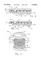
- FIG. 11is a diagrammatic exploded view depicting the component of FIGS. 1-10 together with additional components and apparatus used in an assembly process according to a further embodiment of the invention.
- FIG. 12is a top plan view depicting a partially completed assembly after the process of FIG. 11.
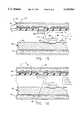
- FIGS. 13 through 17are fragmentary sectional views similar to FIG. 10 but depicting the component together with a semiconductor chip at progressively later stages of the assembly process.
- FIG. 18is a perspective view depicting the completed assembly.
- FIG. 19is a fragmentary sectional view similar to FIG. 10 but depicting a component in accordance with another embodiment of the invention.
- FIGS. 20 through 22are fragmentary, sectional views depicting a component and process in accordance with further embodiments of the invention.
- FIG. 23is a fragmentary, diagrammatic perspective view illustrating operation of a component in accordance with a further embodiment of the invention.
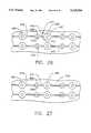
- FIGS. 24 through 27are fragmentary, diagrammatic plan views depicting components in accordance with a further embodiment of the invention.
- FIGS. 28is a fragmentary, schematic sectional view depicting a portion of an assembly process utilized with the component of FIG. 27.
- FIG. 29is a fragmentary, diagrammatic, sectional view depicting components according to a further embodiment of the invention.
- FIGS. 30is a fragmentary, schematic elevational view of an assembly in accordance with yet a further embodiment of the invention.
- a process for manufacturing components according to one embodiment of the inventionbegins with a starting mutilayer sheet 30.
- Mutilayer sheet 30includes a dielectric sheet 34 (FIG. 2), preferably formed from a polymer such polyimide or other known dimensionally stable polymeric films used in the semiconductor industry.
- Dielectric sheet 34desirably is less than about 40 microns thick, more preferably between about 20 and about 30 microns thick and most preferably about 25 microns thick.
- a top layer 36 of electrolytically deposited coppercovers the top surface 35 of dielectric sheet 34, whereas a similar bottom layer 38 covers the opposite, bottom surface 37 of the dielectric sheet.
- the copper layersmay be about 5 to about 25 microns thick.
- mutilayer sheet 30is continuous and substantially uniform over the entire extent of mutilayer sheet 30.
- the mutilayer sheetis stretched taut. While the mutilayer sheet is maintained in a taut condition, it is bonded to a ring-like, generally circular frame 32 so that the mutilayer sheet 30 stretches across the central opening of the frame.
- the mutilayer sheetis bonded to the frame using a suitable high temperature adhesive such as an epoxy resin film, preferably on the order of about 10 microns thick.
- Frame 32is formed from a substantially rigid material having a coefficient of thermal expansion substantially equal to that of the semiconductor part with which the assemblage will be used in later steps. Typically, the semiconductor parts are formed from silicon, and hence the frame has a thermal coefficient of expansion substantially equal to that of silicon. Molybdenum is the preferred frame material.
- bottom layer 38is completely masked by bottom resist 50 whereas top layer 36 is selectively masked in a pattern as shown in FIG. 3.
- the selective maskingcan be performed by a conventional technique of applying an electrophoretic resist, selectively exposing the areas to be covered by the resistor and heat curing and developing the resist to remove the uncured resist material.
- One suitable resistis sold under the designation "Eagle Electrophoretic Resist” by the Shippley Company of Wellesley, Massachusetts. A developer for this resist is available from the same source.
- the patternincludes a vast number of terminal-forming regions 40, typically tens or hundreds of thousands, arranged in a substantially regular pattern including one or more regular, rectilinear grids having a constant pitch P X in one direction and a constant, pitch P y in the other direction along the surface of the sheet. Typically, P y is equal to P X .
- various regions of the sheetwill ultimately be associated with individual chips in a wafer.
- the grids within each such regionmay be continuous with one another, or else may be separated from one another by spaces or interruptions in the grid pattern.
- the regions 41are schematically depicted in FIG. 12 as separated from one another by visible borders 43. However, such visible borders are not always present.
- Each terminal-forming region 40includes an annular mask region 42 defining the periphery of a ring 44 and a central mask region 46 defining a central hole within the ring.
- the rings 44are unmasked.
- the remainder of the sheetis also unmasked so as to form a substantially continuous unmasked region 48 surrounding each of the terminal forming regions 40 and isolated from the ring 44 of each such region by the annular mask unmasked region 42 thereof.
- Continuous region 48desirably extends over most or all of the entire sheet.
- the terminal forming regionhas a modified configuration (not shown) in which the annular mask region 42 is interrupted or eliminated so as to leave the ring 44 connected to the continuous region 48. As further discussed below, these modified terminal forming regions will form potential plane terminals.
- the assemblyis electroplated with an etch resistant metal such as a metal selected from the group consisting of nickel, gold and palladium, most preferably nickel.
- This platingmay be about 1 to 3 microns thick, most preferably about 2 microns thick.
- the plated metalthus covers the ring 44 of each terminal-forming region 40 and also covers the continuous area 48.
- the resistis then stripped away using conventional resist removal techniques, leaving the top copper layer 36 exposed in annular areas 42 and center holes areas 46.
- the assemblyis then subjected to etching using a conventional copper etching solution such as a CuCl etch. During this etching procedure, the etch resistant metal such as nickel previously deposited acts as a resist or etch stop, and protects copper layer 36.
- the etch resistant metalis not present and the copper layer is removed, leaving a pattern as illustrated in FIG. 4, with continuous area 48 and ring areas 44 having copper and nickel and with the center hole areas 46 and annular areas 42 etched to expose the top surface 35 of the dielectric film 34. During this procedure, the bottom copper layer 38 is protected by a bottom resist 50.
- holes 52are formed in dielectric film 34 within the center hole region 46 of each terminal region.
- the holesare formed by ablation using radiant energy such as excimer laser light, desirably at 308 nm wavelength.
- a mask 54 with holes corresponding to the central holes 46 of the terminal regionsis placed above the assemblage so that the holes in the mask are in registration with the central holes 46, and the radiant energy is directed through the holes of the mask.
- the maskis formed from a heat resistant material such as molybdenum. The mask absorbs most of the radiation.
- the copper and nickel rings 44 surrounding central holes 46also act as masks, and limit ablation of the dielectric sheet to the regions within central holes 46.
- the holes or vias 52are lined with a layer of via liner 56 of copper using an electroless plating process.
- the electroless plating processmay include seeding or pretreatment with a palladium salt or other deposition promoter, followed by exposure to the electroless plating solution itself.
- the copper layer 56extends over the bottom of each hole 52, in contact with the bottom copper layer 38 and also extends over the top or upwardly facing surface of each ring 44.
- the copperforms a blind via liner connecting each ring 44 with the bottom copper layer 38.
- the copper layeris about 10 microns thick.
- the bottom resist 50remains in place during this process, and hence the copper is not deposited on the surface of bottom copper layer 38 facing away from sheet 34.
- the top surfacehas a plurality of ring-like terminal structures 44 on its top surface 35 and a blind via liner 56 extending through the dielectric sheet at the center of each such ring-like terminal structure.
- a substantially continuous electrically conductive copper potential plane 48extends over the top surface of the sheet.
- Each ring-like terminal structure 44is surrounded by this continuous layer 48 but electrically isolated therefrom by an annular region 42 (FIG. 3) substantially devoid of conductive material.
- the potential plane terminals (not shown) formed with the modified structure mentioned abovehave their ring-like terminal structures 44 electrically connected to continuous layer 48.
- the copper features on the top surfaceare then electroplated to a thickness of about 2 microns with nickel.
- the plating currentis applied through bottom copper layer 38, and transmitted to the terminals 44 by the via liners 56.
- the plating currentis applied to the potential plane through the potential plane terminals.
- a layer of golddesirably about 0.5 microns thick, is electroplated over the nickel layer.
- the nickel and gold layersform protective, corrosion-resistant coverings on the copper surfaces and edges.
- bottom resist 50is removed and a top resist 58 is applied over the entire top surface of the dielectric sheet 34, and hence over the ring structures 44 and continuous conductive region 48.
- the exposed bottom surface of the bottom copper layer 38is patterned using a resist, photo exposure, curing and developing process similar to those discussed above so as to leave an array of generally dumbbell-shaped lead regions uncovered, and leaving the remainder of the bottom layer 38 covered by the resist.
- Individual leads 60are formed in each region by electroplating a nickel layer 62, typically about 2 microns thick on bottom copper layer 38 and then electroplating a gold layer 64, typically about 5 to about 25 microns thick, desirably about 20 microns thick, on the nickel layer. The resist used to form leads 60 is then removed.
- Each lead 60includes a generally circular, terminal end bulge 66 (FIG. 8), a somewhat smaller, generally circular tip end bulge 68 and an elongated, relatively narrow strip 70 extending between these bulges.
- Leads 60are disposed in a regular, rectilinear grid having the same pitch and arrangement as the grid of ring-like terminals 44 on the top surface.
- each circular bulge 66is concentric with one terminal 44 on the top surface and with the associated via 56.
- an electrically conductive bonding materialis applied in spots 72 on the exposed surfaces on tip end regions 68 of the leads.
- One suitable bonding materialincludes a layer of tin 74, desirably about 10 microns thick and a gold antioxidant layer 76, desirably about 2 microns thick over the tin layer.
- a resistis coated over the exposed surfaces of the leads and photographically patterned and developed to provide holes in the resist at the desired spots for the bonding material.
- the electrically conductive bonding material in each spot 72is applied by electroplating. As discussed further below, other bonding materials and deposition processes may also be employed.
- the top resist 58is left in place and the bottom copper layer 38 is exposed to a sub-etching process using a CuCl etch solution.
- the gold layer 64 and nickel layer 62are substantially unaffected by the etchant and act as etching masks.
- Bottom copper layer 38is attacked in the exposed areas and also at the edges of the leads 60, i.e., at the edges of the gold and nickel layers.
- the copper layeris removed in the exposed areas and progressively removed beneath the leads 60. The extent of inward removal or undercutting from each edge of lead 60 increases progressively with time.
- the process timeis selected so that undercut regions starting from opposite edges of each strip 70 merge with one another, leaving each strip 70 separated from the dielectric sheet 34 by a gap 78.
- the etching or undercutting of the copper layerdoes not proceed all the way to the center of each tip end bulge 68. Rather, the etching process stops short of the center leaving a small, copper button 80 extending from the tip end bulge 68 to the bottom surface 37 of dielectric sheet 34.
- Button 80desirably has a diameter substantially smaller than the diameter of tip end bulge 68.
- the button diameteris less than about 50 microns, and hence the surface area of the button in contact with the lower surface 37 of the dielectric sheet 34 is very small.
- the adhesionis directly related to the surface area of contact, the adhesion is only strong enough to retain the tip end of the lead against gravitational and acceleration forces in normal, gentle handling. The bond between the button 80 and the dielectric sheet can be broken readily in the process discussed below.
- each terminal end button 82is also concentric with the associated via 56, and is metallurgically bonded to the via lining.
- the terminal end buttons 82are also metallurgically bonded to the terminal end bulges 66 of the leads.
- each leadis provided with an electrically continuous, unitary, metallurgically bonded terminal end structure including the terminal end bulge 66, button 82, via liner 56 and ring-like terminal 44 extending through the dielectric sheet from the terminal end 66 of the lead to the top surface of the dielectric sheet.
- each such terminal end structurefirmly secures the terminal end 66 of the lead in place.
- the top resist 58is removed and all of the metallic components, including the terminals or rings 44, via liners 56 and leads 60 are electrolessly plated with a thin covering of gold, desirably about 1 micron thick. This electroless gold layer coats all of the exposed metal surfaces and edges, including the edges and surfaces exposed by etching bottom copper layer 38.
- the plating and etching steps used to form the other featuresalso form fiducial marks including transparent metal free regions 83 schematically indicated in FIG. 12.
- Dielectric sheet 34now constitutes a dielectric connector body.
- the componentmay be handled, shipped and stored in this condition, or else may be assembled immediately to a microelectronic element.
- the precise dimensions of the features in the componentwill depend upon the microelectronic element with which the component will be used. However, for presently popular contact pitch schemes, the following dimensions in Table I can be used (all dimensions in microns).
- the completed component 84 made as discussed above, including the frame 32 and dielectric sheet or connector body 34 with the leads and terminals thereonis assembled with a semiconductor wafer 86 (FIG. 11).
- the waferincludes a large number of individual chip regions 88, each including the elements of a complete semiconductor chip.
- the individual chip regionscorrespond to the regions 41 of the component 84 (FIG. 12).
- Wafer 86also has a vast number of contacts 90 on the top surface 92 of the chip (FIG. 13).
- Component 84is disposed above the top surface of the wafer so that the lower surface 37 of the dielectric sheet 34 faces downwardly, towards the top surface of the chip.
- a perforated, chip engaging vacuum platen 94is disposed beneath the wafer 86, and the wafer is held to the platen by vacuum applied through ports 96.
- Top platen 98includes a transparent plate 102, preferably formed from quartz, surrounded by a metal ring 103.
- the connecting componentis sealingly engaged with top platen, as by an O-ring (not shown) engaged between the circular frame 32 of the connecting component and ring 103. Vacuum is applied through a port 100 to the space between the component and transparent plate 102, thus engaging the flexible sheet firmly with the transparent plate.
- connection component 84While the connecting component 84 and the wafer 86 are engaged with the top and bottom platens, the connection component 84 is brought into registration with the wafer 86 by moving one or both of platens 98 and 94 in the horizontal or X-Y directions and also by rotating one of the platens about a vertical axis, so as to swing the component 84 and wafer 86 relative to one another in the azumithal directions indicated by the arrow theta in FIG. 11. These motions can be controlled using micrometer screw adjusting devices (not shown). During this process, the position of component 84 relative to the chip can be gauged by observing fiducial marks 83 on component 84.
- the top surface of chip 88can be seen through plate 102 and through the film 34.
- the fiducial marks and the relative positions of the component and chipcan be detected either by a human observer or by a machine-vision system.
- the component 84is precisely aligned with the chip so that the tip end 68 of each lead 60 is aligned with the correct contact 90 on the wafer.
- This precise alignmentcan be achieved even over a relatively large component, covering essentially the entire chip.
- the chip and componentmay be about 10-30 cm in diameter.
- the tip ends of the leadsmay be aligned with the contacts with the required precision.
- Several factorscontribute to such precise alignment. Because the dielectric film 34 is continuously held taut throughout the lead-forming process and the aligning process by the same frame 32, the leads remain in position. Also, the tip ends 68 of the leads are secured to the film by buttons 80 (FIG. 10) at all times from the time the leads are formed up to and including the alignment process.
- the tip endscannot move relative to the film.
- frame 32has a coefficient of thermal expansion close to that of the wafer, variations in temperature during the alignment process, and during subsequent steps discussed below, will not tend to move the film relative to the wafer.
- the fiducial marks 83are made in the same etching and plating processes as used to form the other elements of the component, the fiducial marks are in precise registration with the leads.
- the platensare moved toward one another to juxtapose the connecting component closely with the wafer.
- Compressed gasis admitted between plate 102 of the top platen and connecting component 84 so that the compressed gas bears on the top surface of sheet 34 as depicted by the arrows in FIG. 13. This biases the sheet downwardly towards the wafer so that the bonding material 72 at the tip end of each lead is engaged with the aligned contact 90.
- the pressurized gasachieves intimate contact between the component 84, and particularly the bonding material 72 at the tip ends of the leads, over the entire surface of the wafer despite any non-planarity of the component or of the wafer, without applying undesirably high localized stress at any point.
- the assemblyWhile the gas pressure is maintained, the assembly is heated to a temperature sufficient to activate the bonding material in spots 72, and form metallurgical bonds 104 (FIG. 14) between the tip ends of the leads and the contacts 90 of the wafer 86.
- the heating processbrings the assembly to a temperature of about 240° C. for about 150 seconds.
- the tin within each spot 72interdiffuses with the surrounding gold in the contacts 90 and in the lead itself, forming a liquid layer. This layer in turn continues to dissolve gold from the contact pads 90 and from the lead tip ends 68. With increasing gold content, the solidus temperature of the composition rises. At this point, the bond solidifies.
- the bonding processcontinues with an annealing step at a temperature sufficient to permit substantial interdiffusion between gold and tin, typically about 180° C. for about 10 minutes, so as to further enrich the bond with gold and further strengthen the bond.
- a temperature sufficient to permit substantial interdiffusion between gold and tintypically about 180° C. for about 10 minutes, so as to further enrich the bond with gold and further strengthen the bond.
- the tip ends 68 of the leadremain connected to the lower surface 37 of the dielectric sheet 34 by buttons 80. Thus, the tip ends cannot move out of position during the bonding process.
- the dielectric sheet 34 and potential plane layer 48tend to expand at a rate greater than the rate of expansion of the wafer.
- the thermal expansion of the dielectric sheet and potential plane layerare substantially taken up in relieving the tensile stress.
- the actual movement of features on sheet 34 and layer 48 due to thermal expansionis approximately equal to the thermal expansion of frame 32.
- Frame 32has a coefficient of thermal expansion substantially equal to that of wafter 86. Therefore, the features of component 84 remain in alignment with the features of the wafer during the heating process.
- each lead 60has its terminal end 66 securely bonded to a first element of the assembly, i.e., dielectric sheet 34 and has its second end 68 securely bonded to a second element of the assembly, namely, wafer 86.
- the tip end 68 of each leadis offset from the terminal end 66 of the lead in a first horizontal direction parallel to the bottom surface 37 of sheet 34, i.e., the direction D 1 from left to right as seen in FIG. 14.
- the same direction D 1is also indicated in the bottom plan view of the leads (FIG. 8).
- D 1is uniform over the entire component. That is, all of the tip ends are offset from their respective terminal ends in the same direction.
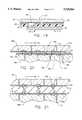
- platen 98is removed and replaced by a metallic vacuum platen 105 having holes 107 extending through it. Vacuum is again applied through platens 105 and 94, thereby holding connection component 84 including dielectric sheet 34 and the wafer 86 firmly against the platens. The platens are then moved relative to one another by moving one or both of the platens so that platen 94 and hence the chip or second element 86 moves vertically, away from platen 105 and away from the dielectric sheet or first element 34, in the direction indicated by the arrow V 1 .
- platen 94 and the wafer or second element 86are moved horizontally relative to platen 105 and the sheet or first element 34 in a horizontal direction D 2 , to the left as seen in FIG. 15.
- the horizontal component of motion of the second element or wafer 86, contacts 94 and tip ends 68 bonded theretois in a second direction D 2 , opposite to the first or original offset direction D 1 .
- the second element 86 and the tip ends 68 of the leadsdescribe an arcuate path A 2 relative to the first element or sheet 34 and relative to the terminal ends 66 of the leads.
- the vertical movementtypically is about 100-500 microns, and the horizontal movement is approximately equal to the vertical movement.
- the same motioncan be restated in terms of a description of the movement of the first element or sheet 34 and terminal ends 66 relative to the second element or wafer 86 and tip ends 68.
- the first elementmoves horizontally relative to the second element in the original offset direction D 1 and simultaneously moves vertically away from the second element, so that the first element describes an arcuate path A 1 relative to the second element.
- the net effect of the relative movement of the two elementsis to move the tip end 68 of each lead horizontally towards the terminal end 66 of the same lead and vertically away from the terminal end of the lead, thus forming each lead into a vertically extensive, generally S-shaped and curved structure as illustrated in FIG. 15.
- each S-shaped structureincludes a first bight 111 adjacent the terminal end 66 of the lead and hence adjacent the first element or connector body 34 and a second bight 113 adjacent the tip end of the lead and hence adjacent the contact 94 and the second element or wafer 86.
- Bight 113is curved in the opposite direction from bight 111.
- the tip ends 68are detached from the bottom surface 37 of the dielectric sheet.
- the copper buttons 80release readily.
- the force required to deform all of the leadsis applied by the atmospheric pressure between the bottom surface 37 of sheet 34 and the top surface 92 of wafer 86. Although the force required for bending each lead will vary with the exact dimensions of the leads, a reasonable value for estimating the forces required is about 2 g per lead.
- the force available from atmospheric pressureis simply the product of standard atmospheric pressure and the area of the wafer or component. Where the available force from atmospheric pressure is not sufficient, the wafer 86 and the sheet 34 can be temporarily bonded to the platens by temporary bonding agents such as a wax.
- a gas or other fluid under superatmospheric pressuremay be introduced between sheet 34 and wafer 86 to increase the forces engaging these elements with the platens and thereby increase the force available to bend the leads.
- a flowable, curable dielectric material 108is injected into the space between the dielectric sheet 34 and the wafer.
- the bottom surface 37 of the connector body or dielectric sheet 34is substantially free of perforations other than the perforations occupied by the terminal structures, such as via liners 56. Therefore, the flowable material is constrained between the connector body of dielectric sheet 34 and wafer 86, and does not cover the terminal features 44 on the top surface of the dielectric sheet.
- the flowable material in its uncured conditionhas a very low viscosity, and also tends to wet the materials of the sheet and wafer so that it effectively fills all of the spaces between the sheet and wafer, penetrating between all of the leads 60.
- Dielectric material 108is selected so that it will form a compliant material such as an elastomer upon cure. Suitable materials include curable silicone such as that sold under the trademark DOW 577 SILICONE by the Dow Corning Corporation of Midland, Mich. and other curable silicones available from Shin-Etsu Silicones of America, Inc.
- the flowable materialmay be injected under external pressure or else may be injected without external pressure and allowed to fill the space only by capillary action.
- the sameAfter injecting the flowable material, the same is cured in place. Depending upon the formulation of the flowable material, such curing may take place spontaneously at room temperature or else may require exposure to heat or radiant energy. A typical cure cycle for the aforementioned silicone materials requires about 160° C. for about 20 minutes.
- solder balls 116are then attached on terminals 44 using a solder ball application technique similar to that applied in conventional flip chip bonding.
- Each solder ball 116may include a spherical core 112 desirably formed from a copper or copper alloy and a coating 114 of a solder such as a lead-tin solder.
- the solder ballsmay include a 200 micron diameter spherical core 112 with a 50 micron thick layer 112 of 63 percent lead--37 percent tin solder.
- a molybdenum sheet(not shown) having holes in a pattern corresponding to the pattern of terminals 44 is applied in registration with the terminals and solder balls are positioned in the holes of the sheet. Each ball is thus aligned with one terminal 44, and an appropriate flux is applied.
- the entire assemblyis heated to a temperature sufficient to melt the solder, as, for example, about 220° C. for about 40 seconds.
- the solderflows and bonds to the terminals 44 as illustrated in FIGS. 17.
- the flux used in solderingis then cleaned from the assembly.
- wafer 86, dielectric sheet 34 and the compliant layer 108are simultaneously severed by sawing along lines 43 (FIG. 12) between the various regions of the dielectric sheet. These lines are in registration with the lines of demarcation between the chips 88 constituting wafer 86.
- the severing operationthus yields individual units as depicted in FIG. 18, each incorporating one region 41 of the dielectric sheet 34, a portion of layer 108 and one chip 88 of the wafer 86.
- the terminals and solder balls 44 and 116 on each regionare disposed in a grid having pitch substantially equal to the pitch of the contacts on the chip.
- the entire unithas surface area, in the horizontal plane, no larger than that of the chip itself.
- Each unitcan then be tested individually by engaging the terminals and solder balls of the entire unit simultaneously with temporary contacts or probes on a test fixture, as by engaging the test fixture and the unit with one another under pressure.
- the compliance of the dielectric material and flexure of sheet 34 and 108aid reliable, simultaneous engagement with the test fixture.
- the same procedurecan be used for prolonged test operation, commonly referred to as "burn-in".
- the unitmay be permanently mounted to a substrate such as a circuit panel or chip package by engaging the solder balls with contact pads on the substrate and heating the assemblage to reflow the solder.
- the soldering techniques per semay be similar to those used in soldering flip-chip or surface mount assemblies.
- each of the solder balls on the unitmay be positioned on a pad of solder paste comprising solder particles dispersed in flux, as commonly used in surface mount attachments. Because the unit is as compact as the original chip, it may be placed close to other chips to form a very compact circuit assembly. After assembly, the unit provides substantial advantages in operation.
- the flexible leads 60, flexible sheet 34 and flexible, compliant material 108permit each terminal 44 and the associated solder ball 116 to move relative to the associated terminal 94 of the chip. This flexibility allows for differential thermal expansion and contraction of the chip and the associated circuit panel or substrate without applying appreciable stresses to the solder joints.
- a connection componenthas a structure similar to that described above but incorporates a reinforcing sheet 57 (FIG. 19) overlying the dielectric sheet 34 and hence overlying the terminals 44' and potential plane layer 48' on the top surface of the dielectric sheet.
- the reinforcing layerextends over the entire surface of the dielectric sheet.
- Both the dielectric sheet and the reinforcing layerdesirably are fastened to a ring-like frame (not shown) similar to the ring-like frame 32 discussed above with reference to FIG. 1.
- Reinforcing layer 57desirably is installed after formation of the features on the top surface, such as the terminals 44, layer 48 and associated vias and via liners.
- Layer 57may be bonded to the dielectric sheet and to the other structures thereon by a releasable adhesive.
- the reinforcing layermay be installed before formation of leads 60' and associated features on the bottom surface 37' of the sheet.
- the reinforcing layerhas a coefficient of thermal expansion substantially equal to that of the wafer.
- Molybdenumis a preferred reinforcing sheet material for use with silicon wafers.
- the reinforcing layerdesirably is in the form of a relatively thin sheet or foil, preferably between about 25 microns and about 250 microns thick.
- the reinforcing layerresists stretching and distortion of the dielectric sheet and thus aids in maintaining precise registration between the tip ends of the leads and the contacts on the wafer.
- the reinforcing layermay also be provided with apertures (not shown) at the areas where the sheet has fiducial marks, so that the fiducial marks can be seen.
- the reinforcing layeris removed after assembly to the wafer, as by deactivating heating to deactivate the adhesive.
- the reinforcing layermay be provided as a permanent layer embedded within the dielectric layer. Such a permanent layer has apertures in alignment with the terminals so that the vias extend through the apertures.
- connection componentcan be fabricated with a lesser number of regions, and can be applied to only a part of a wafer. Also chips may be severed from the wafer to provide individual chips prior to bonding with the component. Thus, the step of bonding the tip ends of the leads may be performed with one chip at a time.
- connection componentscan be fabricated as individual units, each having one chip-size region of the dielectric sheet and each including the leads required to make the connections on a single chip. These individual components may be entirely separate from one another or else may be provided as a semicontinuous tape or sheet for sequential bonding with individual chips.
- the individual chip and the individual portion of the dielectric filmare moved relative to one another in the manner described above so as to the form the leads after bonding.
- processing single-chip-size units or small mutichip unitsfacilitates registration of the tip ends of the leads with the contacts on the chip, and minimizes losses in the event of difficulties during the process.
- microelectronic componentsother than semiconductor wafers or chips can be attached to the connection component and used in the lead-forming process.
- circuit panels or modules having contacts thereoncan be attached to the connection component in substantially the same way as the wafers and chips discussed above.
- connection componentaccording to a further variant is illustrated in FIG. 20.
- the structure according to this variantincludes a dielectric sheet 134 with terminals 144 on a top surface 135 of the sheet.
- Leads 160 including elongated strip-like structures 170extend beneath the bottom surface 137 of the dielectric sheet.
- Each leadincludes a terminal end 166 with a terminal end structure extending through the dielectric sheet 134, from the bottom surface to the top surface and merging with the associated terminal 144.
- These elementsmay be similar to those discussed above with reference to FIGS. 1-19.
- each strip-like lead section 170may be spaced apart from dielectric sheet 134 and may be attached to the dielectric sheet only by the terminal end structure and by a point attachment at the tip end 168 of the lead.
- the component of FIG. 20further includes a positioner sheet 180 formed from a soluble sheet-like material such as a styrene polymer or copolymer.
- Each leadhas a tip end structure such 181 such as a blind via extending through positioner sheet 180 and terminating in an outwardly flaring head on the bottom side 182 of the positioner sheet, i.e., on the side of the positioner sheet remote from the leads and remote from dielectric or top sheet 134.
- the tip end 168 of each leadis offset from the terminal end 161 in a first horizontal direction D 1 .
- dielectric sheet 134 and positioner sheet 180are engaged with platens 198 and 199 respectively.
- the platensare moved relative to one another so that platen 199, positioner sheet 180 and hence the tip ends 168 of the leads move relative to the dielectric sheet 134 and the terminal ends 166 of the leads in an arcuate motion to the position illustrated in FIG. 21.
- the positioner sheet and hence the tip ends of the leadsmove relative to the terminal ends of the leads in a second horizontal direction opposite to first direction D 1 and also move vertically downwardly, away from the dielectric sheet 134 and the terminal ends 166.
- each tip endmoves horizontally towards the associated terminal end but vertically away from the terminal end, so that the leads are deformed to a vertically extensive S-shaped, curved condition.
- all of the S-shaped leadsare curved normal to the major surfaces of the ribbons 160 constituting the leads.
- the S-shaped leadsextend parallel to one another.
- a flowable, curable dielectric material 118is introduced between the sheets 134 and 180 and cured in substantially the same way as discussed above, whereupon the component is removed from the platens.
- positioner sheet 180is removed, preferably by exposure to a solvent, leaving the bottom surface 119 of the dielectric layer exposed.
- the dielectric support layer 118surrounds and supports the leads 160.
- Each of the tip end structures 181is exposed at the bottom surface of the dielectric support layer.
- An electrically conductive bonding material 170is applied on the tip end structures 181 and a layer of a curable, dielectric adhesive 173 is applied over the bottom surface 118 of the dielectric support layer 119.
- the adhesivemay be a so-called snap-cure adhesive having an activation temperature above room temperature but below the temperatures which would be damaging to other components of the assembly.
- One suitable solvent-free, snap-cure adhesiveis sold under the trademark ABLEBOND 967-3 by the Ablestick Electronics Materials and Adhesives Company of Rancho Dominguez, Calif.
- Conductive bonding material 170may be a eutectic bonding material as discussed above, and may be provided with a thin layer of gold to inhibit oxidation. The connection component is now ready for use.
- the bottom surface 119 of the dielectric support layeris juxtaposed with the contact-bearing surface 200 of a semiconductor chip, wafer or other microelectronic element 202, so that the tip ends 168 of the leads, and hence the tip structures 181 and conductive bonding materials 170 are in registration with contacts 204 and the assemblage is then subjected to heat and pressure so as to engage the bottom surface of the support layer 118 with the contact-bearing surface 200 and engage the lead tip ends with the contacts.
- connection componentcan be fabricated as a large component for simultaneous attachment to all of the chips in a single wafer, followed by severance of the chips from the wafer and portions of the dielectric sheet from one another so as to form individual units.
- the connection componentcan be fabricated in a single-chip size, and attached to a single chip after severance of the chip from the wafer.
- positioner sheet 180may be left in place as a part of the final component.
- the positioner sheet 180preferably is formed from a flexible dielectric material similar to that used for top sheet 134.
- the positioner sheetmay be provided with a coating of adhesive on its bottom surface so as to promote formation of a void-free interface between the positioner sheet and the chip or other microelectronic component.
- the first element bearing the terminal ends of the leadsmay itself be a thick, rigid substrate, with internal conductors connected to the terminal ends of the leads. In such an arrangement, the microelectronic element or chip is connected directly to the substrate through the leads, and the microelectronic element is moved relative to the substrate in the lead framing forming step.
- the flowable dielectric material used to form a compliant layer between the dielectric sheet or connector body and the tip or microelectronic elementcan be omitted. This leaves the dielectric sheet or connector body resiliently supported above the chip or microelectronic element by the leads themselves.
- the second element used to move the tip ends of the leadsmay be a tool, such as a platen-like structure, temporarily engaged with or bonded to the tip ends. Such tool may be disengaged from the tip ends after the lead moving step.
- the terminals on the componentneed not be attached to a substrate by soldering.
- Other methodssuch as eutectic bonding, diffusion bonding, and physical engagement of the terminals with contact pads, socket elements or the like can be used.
- the configuration of the terminalsmay be varied to suit these methods.
- Eutectic bonding materials other than the preferred gold-tin compositionscan be employed.
- goldcan form eutectic compositions with germanium, silicon, tin or combinations thereof.
- the tip ends of the leadscan be attached to contacts on the wafer or other microelectronic component by methods other than eutectic bonding as, for example, by diffusion bonding without formation of a liquid phase or by using a solder or metal-bearing polymeric composition.
- Bonding materialscan be applied by methods other than plating as, for example, by dipping the lead tip ends, by silk screening, or by application of a paste.
- the conductive bonding materialmay be provided on the contacts of the microelectronic element, rather than on the lead tip ends.
- bonding methodswhich do not require a distinct bonding material may be employed. Examples of such bonding methods are such as thermosonic and thermocompression bonding of the lead tip ends to the contacts.
- Materials other than gold, such as silver, copper and brassmay be employed for the leads.
- Metals other than copper and nickelcan be used in the terminals, conductive layer and via liners.
- each lead 260may have a terminal end 266 attached to a terminal structure 256 protruding upwardly through the dielectric sheet or connector body (not shown) and may also have a tip end 268 having bonding material 272 or other suitable provision for bonding the tip end to a contact.
- the structure of FIG. 23includes a curved strip 270 connecting the tip end 268 and the terminal end 266 of the lead. In the initial, undeformed condition of the lead shown in solid lines in FIG. 23, the tip end, terminal end and strip 270 are all substantially coplanar, and lie at or close to the bottom surface of the connector body.
- the tip ends 268are bonded to contacts on a microelectronic element such as a wafer, chip or the like.
- the microelectronic elementis then moved, relative to the connector body or dielectric sheet, and hence relative to the terminal ends 266 of the leads, in a downward, straight-line vertical motion.
- Thiscauses the terminal ends 268 to move in a similar unidirectional vertical motion downwardly away from the first element or dielectric sheet.
- the direction of relative motionis indicated by the arrow V 1 ' in FIG. 23.
- the downward displacement of the tip endtends to straighten the initially curved strip 270 as schematically indicated in broken lines at 270'.
- the leadsare straighter than the S-shaped leads discussed above.
- the leadsdo not become entirely straight during the movement process, so that the leads do not tend to pull the tip ends and terminal ends away from the sheet or microelectronic element.
- Processes using initially curved stripscan also incorporate the compound motion as discussed above with reference to FIG. 15.
- the curved strip 270as well, if the relative motion includes a movement of the second element and tip ends 268 in the horizontal direction D 2 ' towards the terminal ends 266, the curved strip 270 can be formed into a curved shape 270".
- each curved leadin its initial, undeformed state, may include an S-shaped strip 370 extending along the bottom surface 337 of the dielectric sheet (FIG. 24) for connector body, between the terminal ends 366 and tip end 368 of each lead.
- the S-shaped lead structuresmay be nested in the manner illustrated in FIG. 24, with the terminal ends 366 disposed in rows and the tip ends 368 disposed in similar but offset rows.
- the curved leadsmay include generally U-shaped structures 380 having a single bight between the terminal end 382 and tip end 384 of each lead. Structures with plural bights can also be employed.
- each leadis not held in position by a button or other bonding structure underlying the tip end. Rather, the tip end of each lead is connected through a frangible element 471 to the terminal end 466 of the next adjacent lead.
- the frangible elementthus retains each tip end 468 in position, adjacent the bottom surface 437 of the connector body or dielectric sheet.
- Frangible element 471may be formed as a continuation of the strip 470 constituting the lead itself, with V-shaped notches 473 extending into the strip from opposite sides thereof.
- the tip ends 468are bonded to the contacts of a chip or other microelectronic element in the same manner as discussed above, as by activating electrically conductive bonding material 472 on the tip ends.
- the microelectronic elementis moved relative to the connector body or dielectric sheet in the same manner as discussed above, so that the tip end 468 of each lead moves vertically away from the body and away from the terminal ends 466, and so that the tip end 468 also moves towards the associated terminal end 466.
- This actionbreaks the frangible element 471 and hence releases each tip end from its connection to the next terminal end.
- Configurations for frangible leadsare disclosed, for example, in PCT Publication WO9403036 published Feb. 3, 1994 (application Ser. No. US93/06930). The disclosure of such PCT Publication, insofar as it describes frangible structures in leads, is hereby incorporated by reference herein.
- the terminal end 568 of each leadis not provided with a bulge, but instead constitutes a continuation of the strip 570 forming the lead.
- the tip end 568 of the leadis again connected to the terminal end 566 of the next adjacent lead by a frangible section 571.
- the dielectric sheet or connector body 534has holes 569 aligned with the terminal ends 568 of the leads.
- the bonding procedure used with this componentemploys a bonding tool 593.
- a tool 593is advanced through holes 569 and engaged with the tip end 568 of each lead in succession so as to bond the tip ends to the contacts.
- the microelectronic element or chip 586is moved relative to the dielectric sheet or connector body 534 in the same manner as discussed above. Once again, this movement breaks the frangible section 571 between the tip end of each lead and the terminal end 566 of the adjacent lead, thus releasing the tip ends and allowing the leads to bend away from the dielectric sheet or connector body 534 in the same manner as described above.
- holes 569may be closed by application of a further film or sheet on the top surface of the dielectric layer.
- a wafer, chip or other microelectronic element 686may itself be provided with leads 660 extending on or over the contact bearing surface 692 of the wafer.
- the fixed or terminal end 666 of each leadmay be permanently connected to the contacts 694 of the chip or wafer and hence permanently connected to the internal circuitry of the chip or wafer, schematically indicated at 695.
- the tip end 668 of each leadmay be detachably secured to the top surface of the chip or wafer, as by a small, loosely adhering button 680, similar to those discussed above.
- the tip endmay optionally be provided with bonding material 672.
- Such a structuremay be fabricated in substantially the same way as the lead structures discussed above.
- the contact bearing surface 692 of the chipmay be provided with a coating 693 of a polyimide or other dielectric material to protect the chip itself during the lead-forming process. This coating may remain in place in the finished assembly.
- the lead-bearing chip or wafer of FIG. 29can be assembled to a connector body 634 having terminal 644 on its bottom surface 637. Each terminal 644 is being connected to internal circuit elements or conductors 645. Each terminal 644 may also be connected to a structure 646 on the top surface of the connector body. Structures 646 are adapted for connection to an external substrate as, for example, by a solder ball process as discussed above. The bonding procedure is substantially the same as that discussed above. Here again, after bonding the two elements are move vertically from one another and desirably also move horizontally, so as to form the desired curved lead structures.
- an assembly according to a further embodiment of the inventionmay include a plurality of microelectronic elements such as a plurality of chips 701, 702 and 703. These elements may be physically attached to a common support or heat sink 704 so that the contact bearing surfaces 705, 706 and 707 are disposed generally coplanar with one another. If the chips are of different thicknesses, sink 704 may have chip mounting surfaces at different heights.
- the microelectronic elementsare disposed at preselected horizontal locations relative to one another. That is, the contact arrays of the various chips are disposed at predetermined locations relative to one another.
- the connector body 734 used with these elementsmay have numerous terminals 744 thereon.
- Terminals 744desirably are disposed in arrays corresponding to the arrays of contacts on the various chips or microelectronic elements.
- the terminals 644are also adapted for connection to an external substrate (not shown).
- Numerous S-shaped leads 760are formed between the terminal 744 and the contacts on the chips by a process as described above.
- connector body 734may be juxtaposed with the assemblage of chips 701, 702 and 703, and the tip ends of the leads on the connector body may be bonded to the contacts on the plural chips simultaneously, whereupon the assemblage of chips is moved relative to the connector body 734.
- chips 701, 702 and 703may themselves have leads thereon as discussed above with reference to FIG.
- the connector body 734has conductors 745 interconnecting various terminals 744 and thus interconnecting the various chips or microelectronic elements with one another to form a multichip module.
- Conductors 745are represented only schematically in FIG. 30. In actual practice, the conductors may include numerous conductors arranged in multiple layers and may also include conductors on the top and bottom surfaces of the connector body 734 itself.
- each chip 701, 702 and 703may be independently aligned with the connector body 734 and bonded to tip ends 768 of the leads 760, before the support or heat sink 704 is bonded to the chips.
- the microelectronic elements connected by the structures and methods according to the present inventionneed not include the chips themselves.
- the microelectronic element itselfmay be a circuit panel or interconnection module such as a rigid printed wiring board, a ceramic module or a metal core wiring layer.
- the leads used to connect elements of this naturetypically are larger than the leads used to connect to chips or wafers.
- the leads used for direct connection to circuit panelsdesirably are formed from a ribbon-like structure between about 10 microns and about 35 microns thick and between about 500 microns and about 2500 microns long.
- the ribbonsdesirably are formed from copper alloy rather than from gold.
Landscapes
- Engineering & Computer Science (AREA)
- Microelectronics & Electronic Packaging (AREA)
- Power Engineering (AREA)
- Computer Hardware Design (AREA)
- General Physics & Mathematics (AREA)
- Condensed Matter Physics & Semiconductors (AREA)
- Physics & Mathematics (AREA)
- Manufacturing & Machinery (AREA)
- Wire Bonding (AREA)
- Lead Frames For Integrated Circuits (AREA)
- Testing Of Individual Semiconductor Devices (AREA)
- Coupling Device And Connection With Printed Circuit (AREA)
- Superconductors And Manufacturing Methods Therefor (AREA)
Abstract
Description
The present invention relates to mounting and connection devices and techniques for use with microelectronic elements such as semiconductor chips.
Complex microelectronic devices such as modern semiconductor chips require numerous connections to other electronic components. For example, a complex microprocessor chip may require many hundreds of connections to external devices.
Semiconductor chips commonly have been connected to electrical traces on mounting substrates by one of three methods: wire bonding, tape automated bonding, and flip-chip bonding. In wire bonding, the chip is positioned on a substrate with a bottom or back surface of the chip abutting the substrate and with the contact-bearing front or top surface of the chip facing upwardly, away from the substrate. Individual gold or aluminum wires are connected between the contacts on the chip and pads on the substrate. In tape automated bonding a flexible dielectric tape with a prefabricated array of leads thereon is positioned over the chip and substrate and the individual leads are bonded to the contacts on the chip and to pads on the substrate. In both wire bonding and conventional tape automated bonding, the pads on the substrate are arranged outside of the area covered by the chip, so that the wires or leads fan out from the chip to the surrounding pads. The area covered by the subassembly as a whole is considerably larger than the area covered by the chip. This makes the entire assembly substantially larger than it otherwise would be. Because the speed with which a microelectronic assembly can operate is inversely related to its size, this presents a serious drawback. Moreover, the wire bonding and tape automated bonding approaches are generally most workable with chips having contacts disposed in rows extending along the periphery of the chip. They generally do not lend themselves to use with chips having contacts disposed in a so-called area array, i.e., a grid-like pattern covering all or a substantial portion of the chip front surface.
In the flip-chip mounting technique, the contact bearing surface of the chip faces towards the substrate. Each contact on the chip is joined by a solder bond to the corresponding pad on the substrate, as by positioning solder balls on the substrate or chip, juxtaposing the chip with the substrate in the front-face-down orientation and momentarily melting or reflowing the solder. The flip-chip technique yields a compact assembly, which occupies an area of the substrate no larger than the area of the chip itself. However, flip-chip assemblies suffer from significant problems with thermal stress. The solder bonds between the chip contacts and substrate are substantially rigid. Changes in the size of the chip and of the substrate due to thermal expansion and contraction in service create substantial stresses in these rigid bonds, which in turn can lead to fatigue failure of the bonds. Moreover, it is difficult to test the chip before attaching it to the substrate, and hence difficult to maintain the required outgoing quality level in the finished assembly, particularly where the assembly includes numerous chips.
Numerous attempts have been made to solve the foregoing problem. Useful solutions are disclosed in commonly assigned U.S. Pat. Nos. 5,148,265 and 5,148,266. Preferred embodiments of the structures disclosed in these patents incorporate flexible, sheet-like structures referred to as "interposers" or "chip carriers". The preferred chip carriers have a plurality of terminals disposed on a flexible, sheet-like top layer. In use, the interposer is disposed on the front or contact bearing surface of the chip with the terminals facing upwardly, away from the chip. The terminals are then connected to the contacts of the chip. Most preferably, this connection is made by bonding prefabricated leads on the interposer to the chip contacts, using a tool engaged with the lead. The completed assembly is then connected to a substrate, as by bonding the terminals of the chip carrier to the substrate. Because the leads and the dielectric layer of the chip carrier are flexible, the terminals on the chip carrier can move relative to the contacts on the chip without imposing significant stresses on the bonds between the leads and the chip, or on the bonds between the terminals and the substrate. Thus, the assembly can compensate for thermal effects. Moreover, the assembly most preferably includes a compliant layer disposed between the terminals on the chip carrier and the face of the chip itself as, for example, an elastomeric layer incorporated in the chip carrier and disposed between the dielectric layer of the chip carrier and the chip. Such a compliant structure permits displacement of the individual terminals independently towards the chip. This permits effective engagement between the subassembly and a test fixture. Thus, a test fixture incorporating numerous electrical contacts can be engaged with all of the terminals in the subassembly despite minor variations in the height of the terminals. The subassembly can be tested before it is bonded to a substrate so as to provide a tested, known, good part to the substrate assembly operation. This in turn provides very substantial economic and quality advantages.
Copending, commonly assigned U.S. patent application Ser. No. 08/190,779, now U.S. Pat. No. 5,455,350, describes a further improvement. Components according to preferred embodiments of the '779 application use a flexible, dielectric top sheet having top and bottom surfaces. A plurality of terminals are mounted on the top sheet. A support layer is disposed underneath the top sheet, the support layer having a bottom surface remote from the top sheet. A plurality of electrically conductive, elongated leads are connected to the terminals on the top sheet and extend generally side by side downwardly from the terminals through the support layer. Each lead has a lower end at the bottom surface of the support layer. The lower ends of the leads have conductive bonding materials as, for example, eutectic bonding metals. The support layer surrounds and supports the leads.
Components of this type can be connected to microelectronic elements such as semiconductor chips or wafers by juxtaposing the bottom surface of the support layer with the contact-bearing surface of the chip so as to bring the lower ends of the leads into engagement with the contacts on the chip, and then subjecting the assembly to elevated temperature and pressure conditions. All of the lower ends of the leads bond to the contacts on the chip substantially simultaneously. The bonded leads connect the terminals of the top sheet with the contacts on the chip. The support layer desirably is either formed from a relatively low-modulus, compliant material, or else is removed and replaced after the lead bonding step with such a compliant material. In the finished assembly, the terminals desirably are movable with respect to the chip to permit testing and to compensate for thermal effects. However, the components and methods of the '779 application provide further advantages, including the ability to make all of the bonds to the chip or other component in a single lamination-like process step. The components and methods of the '779 application are especially advantageous when used with chips or other microelectronic elements having contacts disposed in an area array.
Despite these and other advances in the art, there are still needs for further improvements.
One aspect of the present invention provides methods of making microelectronic lead arrays. Method according to this aspect of the present invention includes the steps of providing a first element having a first surface with a plurality of elongated, flexible leads extending along the first surface, each such lead having a terminal end attached to the first element and a tip end offset from the terminal end in a preselected, first horizontal direction parallel to the first surface. The method also includes the step of simultaneously forming all of the leads by moving all of the tip ends of the leads relative to the terminal ends thereof and relative to the first element so as to bend the tip ends away from the first element.
Desirably, the tip ends of all the leads are attached to a second element, and the step of moving the tip ends of the lead relative to the terminal ends of the leads includes the step of moving the second element relative to the first element. Thus, the second element may be moved, relative to the first element, in a second horizontal direction opposite to the first horizontal direction, i.e., opposite to the terminal end to tip end direction of the leads. The second element preferably also moves in a downward vertical direction, away from the first element, simultaneously with the horizontal movement. The net effect is to move the tip end of each lead horizontally towards its own terminal end and vertically away from the terminal end, thereby deforming the leads towards formed positions in which the leads extend generally vertically downwardly, away from the first element. Methods according to this aspect of the present invention preferably also include the step of injecting a flowable, desirably compliant dielectric material around the leads after the lead-forming step and then curing the flowable material so as to form a dielectric support layer around the leads.
Most preferably, the first element is a flexible, dielectric top sheet having terminal structures extending therethrough at the terminal ends of the leads. The forming process may be used to produce a component for subsequent attachment to a microelectronic element. In processes for making such a component, the second element may be a temporary, removable element as, for example, a sheet of a soluble polymer. This temporary element is removed after the support layer is formed, as by dissolving away the soluble sheet, leaving the tip ends of the leads exposed at the bottom surface of the support layer. Bonding material can be applied to the tip ends of the leads before or after the step of forming the dielectric support layer. The resulting component can be assembled to a chip or other microelectronic element by juxtaposing the exposed surface of the support layer with the contact bearing surface of the element and bonding the tip ends of the leads to the contacts of the chip or other element.
Thus, after the component is connected to the chip or other element, the terminals on the flexible sheet are electrically connected to the contacts of the chip, but are movable with respect to the contacts both in directions parallel to the surface of the chip and towards the surface of the chip. The resulting assembly can be tested readily by engagement with a test probe and can also be assembled readily to a larger substrate. The movability of the terminals will provide compensation for differences in thermal expansion and contraction of the chip and the substrate to which it is mounted..
In a variant of this approach, the second element is a permanent, flexible dielectric sheet, initially positioned adjacent the first sheet. The tip end of each lead is provided with a conductive tip structure, such as a conductive post or via extending through the second dielectric sheet. In the lead-forming step, the second sheet moves away from the first sheet, and the flowable dielectric material is injected between the sheets. The tip structures may be provided with conductive bonding materials, and the resulting component may be connected to a microelectronic element by juxtaposing the surface of the second sheet with the contact-bearing surface of the microelectronic element.
According to a further, and particularly preferred arrangement, the second element is itself a microelectronic element such as a semiconductor chip or wafer. In this arrangement, the step of attaching the tip ends of the leads to the second element includes the step of bonding the tip ends of the leads to the contacts on the chip or other microelectronic element. This step desirably is performed while the leads are in their initial, undeformed positions. Thus, all of the tip ends are bonded simultaneously to all of the contacts on the microelectronic element. Because the leads are in their initial, undeformed positions when bonded to the contacts, the tip positions of the lead tips are well controlled at this stage. This facilitates registration of the lead tips with the contacts. Further, the process lends itself to application of substantial forces between the lead tips and the contacts.
In a particularly preferred arrangement, the second element is a multi-chip unit such as a wafer incorporating a plurality of semiconductor chips having contacts thereon and the first element or sheet extends over a plurality of these chips so that the sheet includes a plurality of regions, one such region corresponding to each such chip. In this arrangement, the step of attaching the tip ends of the leads to the second element preferably includes the step of bonding the tip ends of leads in a plurality of such regions, and desirably in all of such regions, to the contacts on the corresponding chips simultaneously so that each such region is connected to one chip. The method further includes the step of severing the chips from the multichip element or wafer and severing the regions from the sheet so as to form individual units, each including one chip and the associated region of the sheet. Preferably, the method also includes the step of injecting a flowable dielectric material between the wafer and the sheet and curing the dielectric material to form a compliant dielectric support layer after the lead bonding step but before the severing step. The severing step thus includes the step of severing the dielectric support layer so that each unit formed in the severing step will include a portion of the dielectric support layer. Alternatively, the multi-chip unit may include an assembly of chips in the desired configuration for use, such as an assembly of chips mounted to a common heat sink or support, and the first element may include circuitry adapted to interconnect the plural chips. In this variant, the chips are not severed from one another.
Most preferably, the step of bonding the tip ends of the leads to the contacts of the microelectronic element includes the steps of aligning the top sheet or first element with the microelectronic element so that the tips are in registration with the contacts and biasing the sheet towards the microelectronic element while maintaining the registration. Thus, the sheet may be in engagement with a reinforcing structure during the bonding step to aid registration. The reinforcing structure may include a flexible but substantially inextensible foil such as a metallic foil bonded to the sheet. Alternatively or additionally, the reinforcing structure may include a substantially rigid ring having a central opening such that the sheet extends across the central opening and is held taut by the ring. The step of biasing the sheet towards the contact bearing surface may include the step of applying fluid pressure, such as air pressure, to the top surface of the sheet either directly or through a diaphragm or bag so as to maintain uniform pressure over the entire surface of the sheet.
A further aspect of the present invention provides a component for making a microelectronic connection including a first dielectric element having a first or bottom surface and a plurality of elongated flexible leads overlying the first surface of the first element. Each such lead has a terminal end secured to the first element and a tip end movable away from the first element, the tip end of each such lead being offset from the terminal end of the lead in a first horizontal direction parallel to the first surface. Preferably, the dielectric first element is a sheet having a top or second surface opposite from the first surface, and the component also includes electrically conductive terminal structures extending through the sheet at the terminal ends of the leads. Preferably, each lead has an electrically conductive bonding material at the tip end. Thus, the leads may include gold and the bonding material may include a metal selected to form a low-melting eutectic with gold, such as a metal selected from a group consisting of tin, germanium and silicon. The leads desirably are arranged in a regular, grid-like pattern at spacing intervals of less than about 1.25 mm between corresponding features of adjacent leads. Desirably, each lead is between about 200 and about 1000 microns long, about 10 microns to about 25 microns thick and about 10 microns to about 50 microns wide. Components according to this aspect of the invention can be used in methods as discussed above.
Yet another aspect of the invention provides a microelectronic connector including a body such as a flexible dielectric sheet having a bottom surface, there being an area array of terminal structures mounted to the body and exposed on the bottom surface thereof. The connector according to this aspect of the invention includes a plurality of leads, each said lead extending away from said bottom surface, each said lead having a terminal end connected to one said terminal structure and a tip end remote from the terminal structure. The connector according to this aspect of the invention further includes a layer of a compliant dielectric material on said bottom surface of said body, said compliant layer having a bottom surface remote from said body. The compliant layer substantially surrounds and support the leads. The tip ends of the leads protrude from the bottom surface of the compliant layer. Thus, the tip ends of the leads can be engaged with contacts on a microelectronic element by juxtaposing the contact-bearing surface of the microelectronic element with the bottom surface of the compliant layer. Each lead desirably has an electrically conductive bonding material at its tip end for joining the tip end to a contact.
The leads may be generally S-shaped. Each lead may be formed from a ribbon of conductive material having oppositely-directed major surfaces, the ribbon being curved in directions normal to its major surfaces to form the S-shape or other curved configuration of the lead.
Yet another aspect of the invention provides a microelectronic assembly incorporating a microelectronic element having a front surface with an area array of contacts thereon. The assembly includes a connector body having a bottom surface facing toward said front surface of said element but spaced therefrom. The connector body has an area array of terminal structures exposed on said bottom surface and overlying the array of contacts on the microelectronic element.
The assembly includes curved, preferably S-shaped flexible leads extending between the terminal structures and contacts. Here again, each flexible lead desirably is constituted by a metallic ribbon having oppositely-directed major surfaces, the ribbon being curved in directions normal to its major surfaces to form the S-shape.
Assemblies and connectors according to the last-said aspects of the invention can be fabricated readily by the preferred processes discussed above. Preferred assemblies and connectors according the these aspects of the invention provide compact, reliable connections for semiconductor chips and similar elements.
These and other objects, features and advantages of the present invention will be more readily apparent from the detailed description of the preferred embodiments set forth below, taken in conjunction with the accompanying drawings.
FIG. 1 is a plan view of elements used in manufacture of a component according to one embodiment of the invention.
FIG. 2 is a fragmentary schematic sectional view, on an enlarged scale, of one element depicted in FIG. 1.
FIG. 3 is a fragmentary top plan view depicting portions of the element of FIG. 2 but at a later stage in manufacture.
FIGS. 4 through 7 are further fragmentary schematic sectional views similar to FIG. 2 but at progressively later stages during its manufacture.
FIG. 8 is a fragmentary bottom plan view depicting portions of the elements shown in FIGS. 1-7.
FIG. 9 and 10 are further views similar to FIG. 2, depicting the elements at later stages of manufacture.
FIG. 11 is a diagrammatic exploded view depicting the component of FIGS. 1-10 together with additional components and apparatus used in an assembly process according to a further embodiment of the invention.
FIG. 12 is a top plan view depicting a partially completed assembly after the process of FIG. 11.
FIGS. 13 through 17 are fragmentary sectional views similar to FIG. 10 but depicting the component together with a semiconductor chip at progressively later stages of the assembly process.
FIG. 18 is a perspective view depicting the completed assembly.
FIG. 19 is a fragmentary sectional view similar to FIG. 10 but depicting a component in accordance with another embodiment of the invention.
FIGS. 20 through 22 are fragmentary, sectional views depicting a component and process in accordance with further embodiments of the invention.
FIG. 23 is a fragmentary, diagrammatic perspective view illustrating operation of a component in accordance with a further embodiment of the invention.
FIGS. 24 through 27 are fragmentary, diagrammatic plan views depicting components in accordance with a further embodiment of the invention.
FIGS. 28 is a fragmentary, schematic sectional view depicting a portion of an assembly process utilized with the component of FIG. 27.
FIG. 29 is a fragmentary, diagrammatic, sectional view depicting components according to a further embodiment of the invention.
FIGS. 30 is a fragmentary, schematic elevational view of an assembly in accordance with yet a further embodiment of the invention.
A process for manufacturing components according to one embodiment of the invention begins with a startingmutilayer sheet 30.Mutilayer sheet 30 includes a dielectric sheet 34 (FIG. 2), preferably formed from a polymer such polyimide or other known dimensionally stable polymeric films used in the semiconductor industry.Dielectric sheet 34 desirably is less than about 40 microns thick, more preferably between about 20 and about 30 microns thick and most preferably about 25 microns thick. Atop layer 36 of electrolytically deposited copper covers thetop surface 35 ofdielectric sheet 34, whereas a similarbottom layer 38 covers the opposite,bottom surface 37 of the dielectric sheet. The copper layers may be about 5 to about 25 microns thick. In the starting condition illustrated in FIGS. 1 and 2, these layers are continuous and substantially uniform over the entire extent ofmutilayer sheet 30. The mutilayer sheet is stretched taut. While the mutilayer sheet is maintained in a taut condition, it is bonded to a ring-like, generallycircular frame 32 so that themutilayer sheet 30 stretches across the central opening of the frame. The mutilayer sheet is bonded to the frame using a suitable high temperature adhesive such as an epoxy resin film, preferably on the order of about 10 microns thick.Frame 32 is formed from a substantially rigid material having a coefficient of thermal expansion substantially equal to that of the semiconductor part with which the assemblage will be used in later steps. Typically, the semiconductor parts are formed from silicon, and hence the frame has a thermal coefficient of expansion substantially equal to that of silicon. Molybdenum is the preferred frame material.
In the next stage of the process,bottom layer 38 is completely masked by bottom resist 50 whereastop layer 36 is selectively masked in a pattern as shown in FIG. 3. The selective masking can be performed by a conventional technique of applying an electrophoretic resist, selectively exposing the areas to be covered by the resistor and heat curing and developing the resist to remove the uncured resist material. One suitable resist is sold under the designation "Eagle Electrophoretic Resist" by the Shippley Company of Wellesley, Massachusetts. A developer for this resist is available from the same source. The pattern includes a vast number of terminal-formingregions 40, typically tens or hundreds of thousands, arranged in a substantially regular pattern including one or more regular, rectilinear grids having a constant pitch PX in one direction and a constant, pitch Py in the other direction along the surface of the sheet. Typically, Py is equal to PX. As further discussed below, various regions of the sheet will ultimately be associated with individual chips in a wafer. The grids within each such region may be continuous with one another, or else may be separated from one another by spaces or interruptions in the grid pattern. Theregions 41 are schematically depicted in FIG. 12 as separated from one another by visible borders 43. However, such visible borders are not always present. Each terminal-formingregion 40 includes anannular mask region 42 defining the periphery of aring 44 and acentral mask region 46 defining a central hole within the ring. Therings 44 are unmasked. The remainder of the sheet is also unmasked so as to form a substantially continuousunmasked region 48 surrounding each of theterminal forming regions 40 and isolated from thering 44 of each such region by the annular mask unmaskedregion 42 thereof.Continuous region 48 desirably extends over most or all of the entire sheet. At predetermined locations within the array, the terminal forming region has a modified configuration (not shown) in which theannular mask region 42 is interrupted or eliminated so as to leave thering 44 connected to thecontinuous region 48. As further discussed below, these modified terminal forming regions will form potential plane terminals.
After the selective masking has been applied, the assembly is electroplated with an etch resistant metal such as a metal selected from the group consisting of nickel, gold and palladium, most preferably nickel. This plating may be about 1 to 3 microns thick, most preferably about 2 microns thick. The plated metal thus covers thering 44 of each terminal-formingregion 40 and also covers thecontinuous area 48. The resist is then stripped away using conventional resist removal techniques, leaving thetop copper layer 36 exposed inannular areas 42 andcenter holes areas 46. The assembly is then subjected to etching using a conventional copper etching solution such as a CuCl etch. During this etching procedure, the etch resistant metal such as nickel previously deposited acts as a resist or etch stop, and protectscopper layer 36. However, incenter hole areas 46 andannular areas 42, the etch resistant metal is not present and the copper layer is removed, leaving a pattern as illustrated in FIG. 4, withcontinuous area 48 andring areas 44 having copper and nickel and with thecenter hole areas 46 andannular areas 42 etched to expose thetop surface 35 of thedielectric film 34. During this procedure, thebottom copper layer 38 is protected by a bottom resist 50.
In the next stage of the process, holes 52 are formed indielectric film 34 within thecenter hole region 46 of each terminal region. The holes are formed by ablation using radiant energy such as excimer laser light, desirably at 308 nm wavelength. Amask 54 with holes corresponding to thecentral holes 46 of the terminal regions is placed above the assemblage so that the holes in the mask are in registration with thecentral holes 46, and the radiant energy is directed through the holes of the mask. The mask is formed from a heat resistant material such as molybdenum. The mask absorbs most of the radiation. However, the copper and nickel rings 44 surroundingcentral holes 46 also act as masks, and limit ablation of the dielectric sheet to the regions withincentral holes 46.
In the next step of the process, the holes orvias 52 are lined with a layer of vialiner 56 of copper using an electroless plating process. The electroless plating process may include seeding or pretreatment with a palladium salt or other deposition promoter, followed by exposure to the electroless plating solution itself. Thecopper layer 56 extends over the bottom of eachhole 52, in contact with thebottom copper layer 38 and also extends over the top or upwardly facing surface of eachring 44. Thus, the copper forms a blind via liner connecting eachring 44 with thebottom copper layer 38. Desirably, the copper layer is about 10 microns thick. The bottom resist 50 remains in place during this process, and hence the copper is not deposited on the surface ofbottom copper layer 38 facing away fromsheet 34. At this stage of the process, the top surface has a plurality of ring-liketerminal structures 44 on itstop surface 35 and a blind vialiner 56 extending through the dielectric sheet at the center of each such ring-like terminal structure. A substantially continuous electrically conductivecopper potential plane 48 extends over the top surface of the sheet. Each ring-like terminal structure 44 is surrounded by thiscontinuous layer 48 but electrically isolated therefrom by an annular region 42 (FIG. 3) substantially devoid of conductive material. However, the potential plane terminals (not shown) formed with the modified structure mentioned above have their ring-liketerminal structures 44 electrically connected tocontinuous layer 48. The copper features on the top surface are then electroplated to a thickness of about 2 microns with nickel. The plating current is applied throughbottom copper layer 38, and transmitted to theterminals 44 by the vialiners 56. The plating current is applied to the potential plane through the potential plane terminals. A layer of gold, desirably about 0.5 microns thick, is electroplated over the nickel layer. The nickel and gold layers form protective, corrosion-resistant coverings on the copper surfaces and edges.
In the next stage of the process, bottom resist 50 is removed and a top resist 58 is applied over the entire top surface of thedielectric sheet 34, and hence over thering structures 44 and continuousconductive region 48. The exposed bottom surface of thebottom copper layer 38 is patterned using a resist, photo exposure, curing and developing process similar to those discussed above so as to leave an array of generally dumbbell-shaped lead regions uncovered, and leaving the remainder of thebottom layer 38 covered by the resist. Individual leads 60 are formed in each region by electroplating anickel layer 62, typically about 2 microns thick onbottom copper layer 38 and then electroplating agold layer 64, typically about 5 to about 25 microns thick, desirably about 20 microns thick, on the nickel layer. The resist used to form leads 60 is then removed.
Eachlead 60 includes a generally circular, terminal end bulge 66 (FIG. 8), a somewhat smaller, generally circulartip end bulge 68 and an elongated, relativelynarrow strip 70 extending between these bulges. Leads 60 are disposed in a regular, rectilinear grid having the same pitch and arrangement as the grid of ring-like terminals 44 on the top surface. Thus, eachcircular bulge 66 is concentric with oneterminal 44 on the top surface and with the associated via 56. In the next stage of the process, an electrically conductive bonding material is applied inspots 72 on the exposed surfaces ontip end regions 68 of the leads. One suitable bonding material includes a layer oftin 74, desirably about 10 microns thick and agold antioxidant layer 76, desirably about 2 microns thick over the tin layer. Once again, a resist is coated over the exposed surfaces of the leads and photographically patterned and developed to provide holes in the resist at the desired spots for the bonding material. The electrically conductive bonding material in eachspot 72 is applied by electroplating. As discussed further below, other bonding materials and deposition processes may also be employed.
In the next stage of the process, the top resist 58 is left in place and thebottom copper layer 38 is exposed to a sub-etching process using a CuCl etch solution. Thegold layer 64 andnickel layer 62 are substantially unaffected by the etchant and act as etching masks.Bottom copper layer 38 is attacked in the exposed areas and also at the edges of theleads 60, i.e., at the edges of the gold and nickel layers. As the process proceeds, the copper layer is removed in the exposed areas and progressively removed beneath the leads 60. The extent of inward removal or undercutting from each edge oflead 60 increases progressively with time. The process time is selected so that undercut regions starting from opposite edges of eachstrip 70 merge with one another, leaving eachstrip 70 separated from thedielectric sheet 34 by agap 78. However, because the diameter Dtip of eachtip end bulge 68 is larger than the width WS ofstrips 70, the etching or undercutting of the copper layer does not proceed all the way to the center of eachtip end bulge 68. Rather, the etching process stops short of the center leaving a small,copper button 80 extending from thetip end bulge 68 to thebottom surface 37 ofdielectric sheet 34.Button 80 desirably has a diameter substantially smaller than the diameter oftip end bulge 68. Desirably, the button diameter is less than about 50 microns, and hence the surface area of the button in contact with thelower surface 37 of thedielectric sheet 34 is very small. As the adhesion is directly related to the surface area of contact, the adhesion is only strong enough to retain the tip end of the lead against gravitational and acceleration forces in normal, gentle handling. The bond between thebutton 80 and the dielectric sheet can be broken readily in the process discussed below.
The etching process also undercuts inwardly from the periphery of each terminal inbulge 66 so as to form a substantially circularterminal end button 82 concentric with theterminal end bulge 66 of each lead. Eachterminal end button 82 is also concentric with the associated via 56, and is metallurgically bonded to the via lining. Theterminal end buttons 82 are also metallurgically bonded to the terminal end bulges 66 of the leads. Thus, each lead is provided with an electrically continuous, unitary, metallurgically bonded terminal end structure including theterminal end bulge 66,button 82, vialiner 56 and ring-like terminal 44 extending through the dielectric sheet from theterminal end 66 of the lead to the top surface of the dielectric sheet. Each such terminal end structure firmly secures theterminal end 66 of the lead in place. Following these stages, the top resist 58 is removed and all of the metallic components, including the terminals or rings 44, vialiners 56 and leads 60 are electrolessly plated with a thin covering of gold, desirably about 1 micron thick. This electroless gold layer coats all of the exposed metal surfaces and edges, including the edges and surfaces exposed by etchingbottom copper layer 38.
The plating and etching steps used to form the other features also form fiducial marks including transparent metal free regions 83 schematically indicated in FIG. 12.
At this stage of the process, the component is complete. The dielectric sheet is still secured within frame 32 (FIG. 1), and thedielectric sheet 34 remains in a taut condition.Dielectric sheet 34 now constitutes a dielectric connector body. The component may be handled, shipped and stored in this condition, or else may be assembled immediately to a microelectronic element. The precise dimensions of the features in the component will depend upon the microelectronic element with which the component will be used. However, for presently popular contact pitch schemes, the following dimensions in Table I can be used (all dimensions in microns).
TABLE I ______________________________________ Pitch (P.sub.x, P.sub.y) 1000 500 300 200Inner diameter 100 100 75 50 of ringlike terminals 44(d.sub.i) Outer Diameter (d.sub.o) of terminals 250 250 150 100 Thickness ofTop Copper Layer 36 10 10 5 5 Diameter ofTerminal End Bulge 66 150 150 125 100 Thickness of Bottom Copper 15 10 5 5Layer 38 Diameter of Tip End Bulge 68 (D.sub.tip) 100 100 75 50 Length (L.sub.1) (Center of terminal 1000 750 500 300end bulge 66 to center of tip end bulge 68) Width of Strip 70 (W.sub.s) 35 25 20 15 ______________________________________
In an attachment process according to a further embodiment of the invention, the completedcomponent 84 made as discussed above, including theframe 32 and dielectric sheet orconnector body 34 with the leads and terminals thereon is assembled with a semiconductor wafer 86 (FIG. 11). The wafer includes a large number ofindividual chip regions 88, each including the elements of a complete semiconductor chip. The individual chip regions correspond to theregions 41 of the component 84 (FIG. 12).Wafer 86 also has a vast number ofcontacts 90 on thetop surface 92 of the chip (FIG. 13).Component 84 is disposed above the top surface of the wafer so that thelower surface 37 of thedielectric sheet 34 faces downwardly, towards the top surface of the chip. A perforated, chip engagingvacuum platen 94 is disposed beneath thewafer 86, and the wafer is held to the platen by vacuum applied throughports 96.
While the connectingcomponent 84 and thewafer 86 are engaged with the top and bottom platens, theconnection component 84 is brought into registration with thewafer 86 by moving one or both ofplatens component 84 andwafer 86 relative to one another in the azumithal directions indicated by the arrow theta in FIG. 11. These motions can be controlled using micrometer screw adjusting devices (not shown). During this process, the position ofcomponent 84 relative to the chip can be gauged by observing fiducial marks 83 oncomponent 84. Inasmuch as thedielectric film 34 of the component is transparent, the top surface ofchip 88 can be seen throughplate 102 and through thefilm 34. Thus, the fiducial marks and the relative positions of the component and chip can be detected either by a human observer or by a machine-vision system.
Thecomponent 84 is precisely aligned with the chip so that thetip end 68 of each lead 60 is aligned with thecorrect contact 90 on the wafer. This precise alignment can be achieved even over a relatively large component, covering essentially the entire chip. For example, the chip and component may be about 10-30 cm in diameter. Even over this large area, however, the tip ends of the leads may be aligned with the contacts with the required precision. Several factors contribute to such precise alignment. Because thedielectric film 34 is continuously held taut throughout the lead-forming process and the aligning process by thesame frame 32, the leads remain in position. Also, the tip ends 68 of the leads are secured to the film by buttons 80 (FIG. 10) at all times from the time the leads are formed up to and including the alignment process. Therefore, the tip ends cannot move relative to the film. Moreover, becauseframe 32 has a coefficient of thermal expansion close to that of the wafer, variations in temperature during the alignment process, and during subsequent steps discussed below, will not tend to move the film relative to the wafer. Also, because the fiducial marks 83 are made in the same etching and plating processes as used to form the other elements of the component, the fiducial marks are in precise registration with the leads.
While the component and chip are maintained in precise alignment, the platens are moved toward one another to juxtapose the connecting component closely with the wafer. Compressed gas is admitted betweenplate 102 of the top platen and connectingcomponent 84 so that the compressed gas bears on the top surface ofsheet 34 as depicted by the arrows in FIG. 13. This biases the sheet downwardly towards the wafer so that thebonding material 72 at the tip end of each lead is engaged with the alignedcontact 90. The pressurized gas achieves intimate contact between thecomponent 84, and particularly thebonding material 72 at the tip ends of the leads, over the entire surface of the wafer despite any non-planarity of the component or of the wafer, without applying undesirably high localized stress at any point.
While the gas pressure is maintained, the assembly is heated to a temperature sufficient to activate the bonding material inspots 72, and form metallurgical bonds 104 (FIG. 14) between the tip ends of the leads and thecontacts 90 of thewafer 86. Preferably, the heating process brings the assembly to a temperature of about 240° C. for about 150 seconds. The tin within eachspot 72 interdiffuses with the surrounding gold in thecontacts 90 and in the lead itself, forming a liquid layer. This layer in turn continues to dissolve gold from thecontact pads 90 and from the lead tip ends 68. With increasing gold content, the solidus temperature of the composition rises. At this point, the bond solidifies. The bonding process continues with an annealing step at a temperature sufficient to permit substantial interdiffusion between gold and tin, typically about 180° C. for about 10 minutes, so as to further enrich the bond with gold and further strengthen the bond. During this entire process, the tip ends 68 of the lead remain connected to thelower surface 37 of thedielectric sheet 34 bybuttons 80. Thus, the tip ends cannot move out of position during the bonding process.
Aswafer 86 andcomponent 84 are heated during the bonding process, thedielectric sheet 34 andpotential plane layer 48 tend to expand at a rate greater than the rate of expansion of the wafer. However, because the dielectric sheet and potential plane are held under tension byframe 32, the thermal expansion of the dielectric sheet and potential plane layer are substantially taken up in relieving the tensile stress. The actual movement of features onsheet 34 andlayer 48 due to thermal expansion is approximately equal to the thermal expansion offrame 32.Frame 32, in turn, has a coefficient of thermal expansion substantially equal to that ofwafter 86. Therefore, the features ofcomponent 84 remain in alignment with the features of the wafer during the heating process.
At this stage of the process, in the condition illustrated in FIG. 14, each lead 60 has itsterminal end 66 securely bonded to a first element of the assembly, i.e.,dielectric sheet 34 and has itssecond end 68 securely bonded to a second element of the assembly, namely,wafer 86. Thetip end 68 of each lead is offset from theterminal end 66 of the lead in a first horizontal direction parallel to thebottom surface 37 ofsheet 34, i.e., the direction D1 from left to right as seen in FIG. 14. The same direction D1 is also indicated in the bottom plan view of the leads (FIG. 8). D1 is uniform over the entire component. That is, all of the tip ends are offset from their respective terminal ends in the same direction.
In the next stage of the process,platen 98 is removed and replaced by ametallic vacuum platen 105 havingholes 107 extending through it. Vacuum is again applied throughplatens connection component 84 includingdielectric sheet 34 and thewafer 86 firmly against the platens. The platens are then moved relative to one another by moving one or both of the platens so thatplaten 94 and hence the chip orsecond element 86 moves vertically, away fromplaten 105 and away from the dielectric sheet orfirst element 34, in the direction indicated by the arrow V1. At the same time,platen 94 and the wafer orsecond element 86 are moved horizontally relative toplaten 105 and the sheet orfirst element 34 in a horizontal direction D2, to the left as seen in FIG. 15. Stated another way, the horizontal component of motion of the second element orwafer 86,contacts 94 and tip ends 68 bonded thereto is in a second direction D2, opposite to the first or original offset direction D1. Thus, thesecond element 86 and the tip ends 68 of the leads describe an arcuate path A2 relative to the first element orsheet 34 and relative to the terminal ends 66 of the leads. The vertical movement typically is about 100-500 microns, and the horizontal movement is approximately equal to the vertical movement.
The same motion can be restated in terms of a description of the movement of the first element orsheet 34 and terminal ends 66 relative to the second element orwafer 86 and tip ends 68. In that alternative frame of reference, the first element moves horizontally relative to the second element in the original offset direction D1 and simultaneously moves vertically away from the second element, so that the first element describes an arcuate path A1 relative to the second element. However described, the net effect of the relative movement of the two elements is to move thetip end 68 of each lead horizontally towards theterminal end 66 of the same lead and vertically away from the terminal end of the lead, thus forming each lead into a vertically extensive, generally S-shaped and curved structure as illustrated in FIG. 15.
The S-shaped lead is bent normal to the original top and bottom surfaces of the ribbon orstrip 70 constitutinglead 60. That is, the curvature of the strip in directions normal to the major surfaces of the ribbon, i.e., the original top and bottom surfaces of the ribbon. Also, as seen in FIG. 15, each S-shaped structure includes afirst bight 111 adjacent theterminal end 66 of the lead and hence adjacent the first element orconnector body 34 and asecond bight 113 adjacent the tip end of the lead and hence adjacent thecontact 94 and the second element orwafer 86.Bight 113 is curved in the opposite direction frombight 111. Those portions of the leads constituting thetip end 66 and theterminal end 68 remain generally in their original orientations, so that the original top and bottom surfaces or major surfaces of the lead in these regions continue to face upwardly and downwardly. Although only a single lead is depicted in FIG. 15, it should be appreciated that all of the leads are formed simultaneously in the same manner during the lead-forming process. Thus, all of the leads have the same S-shaped curvature and all of the S-leads extend parallel to one another, in the same orientation.
During the lead-forming process, the tip ends 68 are detached from thebottom surface 37 of the dielectric sheet. Thecopper buttons 80 release readily. The force required to deform all of the leads is applied by the atmospheric pressure between thebottom surface 37 ofsheet 34 and thetop surface 92 ofwafer 86. Although the force required for bending each lead will vary with the exact dimensions of the leads, a reasonable value for estimating the forces required is about 2 g per lead. The force available from atmospheric pressure is simply the product of standard atmospheric pressure and the area of the wafer or component. Where the available force from atmospheric pressure is not sufficient, thewafer 86 and thesheet 34 can be temporarily bonded to the platens by temporary bonding agents such as a wax. Alternatively, where appropriate gasketing is arranged around the periphery of the platens, a gas or other fluid under superatmospheric pressure may be introduced betweensheet 34 andwafer 86 to increase the forces engaging these elements with the platens and thereby increase the force available to bend the leads.
After the lead-forming step, while thedielectric sheet 34 andwafer 86 are still in their moved positions, and still engaged with theplatens dielectric material 108 is injected into the space between thedielectric sheet 34 and the wafer. Thebottom surface 37 of the connector body ordielectric sheet 34 is substantially free of perforations other than the perforations occupied by the terminal structures, such as vialiners 56. Therefore, the flowable material is constrained between the connector body ofdielectric sheet 34 andwafer 86, and does not cover the terminal features 44 on the top surface of the dielectric sheet. Preferably, the flowable material in its uncured condition has a very low viscosity, and also tends to wet the materials of the sheet and wafer so that it effectively fills all of the spaces between the sheet and wafer, penetrating between all of the leads 60.Dielectric material 108 is selected so that it will form a compliant material such as an elastomer upon cure. Suitable materials include curable silicone such as that sold under the trademark DOW 577 SILICONE by the Dow Corning Corporation of Midland, Mich. and other curable silicones available from Shin-Etsu Silicones of America, Inc. The flowable material may be injected under external pressure or else may be injected without external pressure and allowed to fill the space only by capillary action. After injecting the flowable material, the same is cured in place. Depending upon the formulation of the flowable material, such curing may take place spontaneously at room temperature or else may require exposure to heat or radiant energy. A typical cure cycle for the aforementioned silicone materials requires about 160° C. for about 20 minutes.
After curing, the assembly including the dielectrictop sheet 34,compliant dielectric layer 108 andwafer 86, together with theterminals 44 connected tocontacts 94 byleads 60, is removed from the platens. The continuouspotential plane layer 48 on the top surface ofsheet 34 is then coated with a conventionalsolder mask layer 110, leaving openings at theterminals 44.Solder balls 116 are then attached onterminals 44 using a solder ball application technique similar to that applied in conventional flip chip bonding. Eachsolder ball 116 may include aspherical core 112 desirably formed from a copper or copper alloy and acoating 114 of a solder such as a lead-tin solder. For example, the solder balls may include a 200 micron diameterspherical core 112 with a 50 micronthick layer 112 of 63 percent lead--37 percent tin solder. A molybdenum sheet (not shown) having holes in a pattern corresponding to the pattern ofterminals 44 is applied in registration with the terminals and solder balls are positioned in the holes of the sheet. Each ball is thus aligned with oneterminal 44, and an appropriate flux is applied. The entire assembly is heated to a temperature sufficient to melt the solder, as, for example, about 220° C. for about 40 seconds. The solder flows and bonds to theterminals 44 as illustrated in FIGS. 17. The flux used in soldering is then cleaned from the assembly.
Following the soldering operation,wafer 86,dielectric sheet 34 and thecompliant layer 108 are simultaneously severed by sawing along lines 43 (FIG. 12) between the various regions of the dielectric sheet. These lines are in registration with the lines of demarcation between thechips 88 constitutingwafer 86. The severing operation thus yields individual units as depicted in FIG. 18, each incorporating oneregion 41 of thedielectric sheet 34, a portion oflayer 108 and onechip 88 of thewafer 86. The terminals andsolder balls sheet
After testing and burn-in, if required, the unit may be permanently mounted to a substrate such as a circuit panel or chip package by engaging the solder balls with contact pads on the substrate and heating the assemblage to reflow the solder. The soldering techniques per se may be similar to those used in soldering flip-chip or surface mount assemblies. For example, each of the solder balls on the unit may be positioned on a pad of solder paste comprising solder particles dispersed in flux, as commonly used in surface mount attachments. Because the unit is as compact as the original chip, it may be placed close to other chips to form a very compact circuit assembly. After assembly, the unit provides substantial advantages in operation. Thus, the flexible leads 60,flexible sheet 34 and flexible,compliant material 108 permit each terminal 44 and the associatedsolder ball 116 to move relative to the associatedterminal 94 of the chip. This flexibility allows for differential thermal expansion and contraction of the chip and the associated circuit panel or substrate without applying appreciable stresses to the solder joints.
A connection component according to a further embodiment of the invention has a structure similar to that described above but incorporates a reinforcing sheet 57 (FIG. 19) overlying thedielectric sheet 34 and hence overlying the terminals 44' and potential plane layer 48' on the top surface of the dielectric sheet. The reinforcing layer extends over the entire surface of the dielectric sheet. Both the dielectric sheet and the reinforcing layer desirably are fastened to a ring-like frame (not shown) similar to the ring-like frame 32 discussed above with reference to FIG. 1. Reinforcinglayer 57 desirably is installed after formation of the features on the top surface, such as theterminals 44,layer 48 and associated vias and via liners.Layer 57 may be bonded to the dielectric sheet and to the other structures thereon by a releasable adhesive. The reinforcing layer may be installed before formation ofleads 60' and associated features on the bottom surface 37' of the sheet. Preferably, the reinforcing layer has a coefficient of thermal expansion substantially equal to that of the wafer. Molybdenum is a preferred reinforcing sheet material for use with silicon wafers. The reinforcing layer desirably is in the form of a relatively thin sheet or foil, preferably between about 25 microns and about 250 microns thick. During assembly of the connection component to the wafer, fluid pressure is applied on the reinforcing layer and hence applied to the dielectric sheet 34' through the reinforcing layer. The reinforcing layer resists stretching and distortion of the dielectric sheet and thus aids in maintaining precise registration between the tip ends of the leads and the contacts on the wafer. The reinforcing layer may also be provided with apertures (not shown) at the areas where the sheet has fiducial marks, so that the fiducial marks can be seen. The reinforcing layer is removed after assembly to the wafer, as by deactivating heating to deactivate the adhesive. In a variant of this approach, the reinforcing layer may be provided as a permanent layer embedded within the dielectric layer. Such a permanent layer has apertures in alignment with the terminals so that the vias extend through the apertures.
In further variants of the invention, the connection component can be fabricated with a lesser number of regions, and can be applied to only a part of a wafer. Also chips may be severed from the wafer to provide individual chips prior to bonding with the component. Thus, the step of bonding the tip ends of the leads may be performed with one chip at a time. In such an arrangement, the connection components can be fabricated as individual units, each having one chip-size region of the dielectric sheet and each including the leads required to make the connections on a single chip. These individual components may be entirely separate from one another or else may be provided as a semicontinuous tape or sheet for sequential bonding with individual chips. In any such arrangement, the individual chip and the individual portion of the dielectric film are moved relative to one another in the manner described above so as to the form the leads after bonding. Processing the entire wafer simultaneously offer significant economies in processing and simplicity. Only one severing operation is required to sever both the dielectric sheets and the wafer to form the units. However, processing single-chip-size units or small mutichip units facilitates registration of the tip ends of the leads with the contacts on the chip, and minimizes losses in the event of difficulties during the process.
In other variants according to the present invention, microelectronic components other than semiconductor wafers or chips can be attached to the connection component and used in the lead-forming process. For example, circuit panels or modules having contacts thereon can be attached to the connection component in substantially the same way as the wafers and chips discussed above.
A connection component according to a further variant is illustrated in FIG. 20. The structure according to this variant includes adielectric sheet 134 withterminals 144 on atop surface 135 of the sheet.Leads 160 including elongated strip-like structures 170 extend beneath thebottom surface 137 of the dielectric sheet. Each lead includes aterminal end 166 with a terminal end structure extending through thedielectric sheet 134, from the bottom surface to the top surface and merging with the associatedterminal 144. These elements may be similar to those discussed above with reference to FIGS. 1-19. For example, each strip-like lead section 170 may be spaced apart fromdielectric sheet 134 and may be attached to the dielectric sheet only by the terminal end structure and by a point attachment at thetip end 168 of the lead.
The component of FIG. 20 further includes apositioner sheet 180 formed from a soluble sheet-like material such as a styrene polymer or copolymer. Each lead has a tip end structure such 181 such as a blind via extending throughpositioner sheet 180 and terminating in an outwardly flaring head on thebottom side 182 of the positioner sheet, i.e., on the side of the positioner sheet remote from the leads and remote from dielectric ortop sheet 134. Here again, in the initial, undeformed condition illustrated in FIG. 20, thetip end 168 of each lead is offset from the terminal end 161 in a first horizontal direction D1.
In a forming process,dielectric sheet 134 andpositioner sheet 180 are engaged withplatens platen 199,positioner sheet 180 and hence the tip ends 168 of the leads move relative to thedielectric sheet 134 and the terminal ends 166 of the leads in an arcuate motion to the position illustrated in FIG. 21. The positioner sheet and hence the tip ends of the leads move relative to the terminal ends of the leads in a second horizontal direction opposite to first direction D1 and also move vertically downwardly, away from thedielectric sheet 134 and the terminal ends 166. Again, each tip end moves horizontally towards the associated terminal end but vertically away from the terminal end, so that the leads are deformed to a vertically extensive S-shaped, curved condition. Here again, all of the S-shaped leads are curved normal to the major surfaces of theribbons 160 constituting the leads. Also, the S-shaped leads extend parallel to one another.
Following this operation, a flowable, curabledielectric material 118 is introduced between thesheets positioner sheet 180 is removed, preferably by exposure to a solvent, leaving thebottom surface 119 of the dielectric layer exposed. In this condition, thedielectric support layer 118 surrounds and supports the leads 160. Each of thetip end structures 181 is exposed at the bottom surface of the dielectric support layer. An electricallyconductive bonding material 170 is applied on thetip end structures 181 and a layer of a curable,dielectric adhesive 173 is applied over thebottom surface 118 of thedielectric support layer 119. The adhesive may be a so-called snap-cure adhesive having an activation temperature above room temperature but below the temperatures which would be damaging to other components of the assembly. One suitable solvent-free, snap-cure adhesive is sold under the trademark ABLEBOND 967-3 by the Ablestick Electronics Materials and Adhesives Company of Rancho Dominguez, Calif.Conductive bonding material 170 may be a eutectic bonding material as discussed above, and may be provided with a thin layer of gold to inhibit oxidation. The connection component is now ready for use.
In use, thebottom surface 119 of the dielectric support layer is juxtaposed with the contact-bearingsurface 200 of a semiconductor chip, wafer or othermicroelectronic element 202, so that the tip ends 168 of the leads, and hence thetip structures 181 andconductive bonding materials 170 are in registration withcontacts 204 and the assemblage is then subjected to heat and pressure so as to engage the bottom surface of thesupport layer 118 with the contact-bearingsurface 200 and engage the lead tip ends with the contacts. Under these conditions, the adhesive 173 forms a void-free interface betweensupport layer 118 andelement 202 and the conductive bonding material forms a metallurgical bond and electrical connection between the leads and the contact of the microelectronic element, thereby connecting theterminals 144 to the contacts. The resulting assembly can be mounted to a circuit panel or other substrate in the same manner as the assemblies discussed above and provides similar advantages. Here again, the connection component can be fabricated as a large component for simultaneous attachment to all of the chips in a single wafer, followed by severance of the chips from the wafer and portions of the dielectric sheet from one another so as to form individual units. Alternatively, the connection component can be fabricated in a single-chip size, and attached to a single chip after severance of the chip from the wafer.
In a further variant,positioner sheet 180 may be left in place as a part of the final component. In this case, thepositioner sheet 180 preferably is formed from a flexible dielectric material similar to that used fortop sheet 134. The positioner sheet may be provided with a coating of adhesive on its bottom surface so as to promote formation of a void-free interface between the positioner sheet and the chip or other microelectronic component. In a further variant, the first element bearing the terminal ends of the leads may itself be a thick, rigid substrate, with internal conductors connected to the terminal ends of the leads. In such an arrangement, the microelectronic element or chip is connected directly to the substrate through the leads, and the microelectronic element is moved relative to the substrate in the lead framing forming step. In the structures and methods discussed above, the flowable dielectric material used to form a compliant layer between the dielectric sheet or connector body and the tip or microelectronic element can be omitted. This leaves the dielectric sheet or connector body resiliently supported above the chip or microelectronic element by the leads themselves.
According to a further variant, the second element used to move the tip ends of the leads may be a tool, such as a platen-like structure, temporarily engaged with or bonded to the tip ends. Such tool may be disengaged from the tip ends after the lead moving step.
The terminals on the component need not be attached to a substrate by soldering. Other methods, such as eutectic bonding, diffusion bonding, and physical engagement of the terminals with contact pads, socket elements or the like can be used. The configuration of the terminals may be varied to suit these methods. Eutectic bonding materials other than the preferred gold-tin compositions can be employed. Thus, gold can form eutectic compositions with germanium, silicon, tin or combinations thereof. The tip ends of the leads can be attached to contacts on the wafer or other microelectronic component by methods other than eutectic bonding as, for example, by diffusion bonding without formation of a liquid phase or by using a solder or metal-bearing polymeric composition. Bonding materials can be applied by methods other than plating as, for example, by dipping the lead tip ends, by silk screening, or by application of a paste. The conductive bonding material may be provided on the contacts of the microelectronic element, rather than on the lead tip ends. Alternatively, bonding methods which do not require a distinct bonding material may be employed. Examples of such bonding methods are such as thermosonic and thermocompression bonding of the lead tip ends to the contacts. Materials other than gold, such as silver, copper and brass may be employed for the leads. Metals other than copper and nickel can be used in the terminals, conductive layer and via liners.
As illustrated in FIG. 23, each lead 260 may have aterminal end 266 attached to aterminal structure 256 protruding upwardly through the dielectric sheet or connector body (not shown) and may also have atip end 268 havingbonding material 272 or other suitable provision for bonding the tip end to a contact. These elements may be similar to the corresponding elements of the structures discussed above. The structure of FIG. 23 includes acurved strip 270 connecting thetip end 268 and theterminal end 266 of the lead. In the initial, undeformed condition of the lead shown in solid lines in FIG. 23, the tip end, terminal end andstrip 270 are all substantially coplanar, and lie at or close to the bottom surface of the connector body. Using a connection process similar to that discussed above with reference to FIGS. 13-15, the tip ends 268 are bonded to contacts on a microelectronic element such as a wafer, chip or the like.
After bonding, the microelectronic element is then moved, relative to the connector body or dielectric sheet, and hence relative to the terminal ends 266 of the leads, in a downward, straight-line vertical motion. This causes the terminal ends 268 to move in a similar unidirectional vertical motion downwardly away from the first element or dielectric sheet. The direction of relative motion is indicated by the arrow V1 ' in FIG. 23. The downward displacement of the tip end tends to straighten the initiallycurved strip 270 as schematically indicated in broken lines at 270'. Thus, after the movement, the leads are straighter than the S-shaped leads discussed above. Most preferably however, the leads do not become entirely straight during the movement process, so that the leads do not tend to pull the tip ends and terminal ends away from the sheet or microelectronic element. Processes using initially curved strips can also incorporate the compound motion as discussed above with reference to FIG. 15. Thus, with thecurved strip 270 as well, if the relative motion includes a movement of the second element and tip ends 268 in the horizontal direction D2 ' towards the terminal ends 266, thecurved strip 270 can be formed into acurved shape 270".
The initially curved leads may be arranged in different ways on the connector body or dielectric sheet. For example, each curved lead, in its initial, undeformed state, may include an S-shapedstrip 370 extending along thebottom surface 337 of the dielectric sheet (FIG. 24) for connector body, between the terminal ends 366 and tip end 368 of each lead. The S-shaped lead structures may be nested in the manner illustrated in FIG. 24, with the terminal ends 366 disposed in rows and the tip ends 368 disposed in similar but offset rows. Alternatively, the curved leads may include generallyU-shaped structures 380 having a single bight between theterminal end 382 and tip end 384 of each lead. Structures with plural bights can also be employed.
In the component of FIG. 26, thetip end 468 of each lead is not held in position by a button or other bonding structure underlying the tip end. Rather, the tip end of each lead is connected through afrangible element 471 to theterminal end 466 of the next adjacent lead. The frangible element thus retains eachtip end 468 in position, adjacent thebottom surface 437 of the connector body or dielectric sheet.Frangible element 471 may be formed as a continuation of thestrip 470 constituting the lead itself, with V-shapednotches 473 extending into the strip from opposite sides thereof. In the assembly process, the tip ends 468 are bonded to the contacts of a chip or other microelectronic element in the same manner as discussed above, as by activating electricallyconductive bonding material 472 on the tip ends. After bonding, the microelectronic element is moved relative to the connector body or dielectric sheet in the same manner as discussed above, so that thetip end 468 of each lead moves vertically away from the body and away from the terminal ends 466, and so that thetip end 468 also moves towards the associatedterminal end 466. This action breaks thefrangible element 471 and hence releases each tip end from its connection to the next terminal end. Configurations for frangible leads are disclosed, for example, in PCT Publication WO9403036 published Feb. 3, 1994 (application Ser. No. US93/06930). The disclosure of such PCT Publication, insofar as it describes frangible structures in leads, is hereby incorporated by reference herein.
In the component of FIG. 27, theterminal end 568 of each lead is not provided with a bulge, but instead constitutes a continuation of thestrip 570 forming the lead. Thetip end 568 of the lead is again connected to theterminal end 566 of the next adjacent lead by afrangible section 571. In this component, the dielectric sheet orconnector body 534 hasholes 569 aligned with the terminal ends 568 of the leads. As illustrated in FIG. 28, the bonding procedure used with this component employs a bonding tool 593. After positioning sheet orconnector body 534 and the leads thereon in alignment with thecontacts 594 on the microelectronic element orchip 586, a tool 593 is advanced throughholes 569 and engaged with thetip end 568 of each lead in succession so as to bond the tip ends to the contacts. After such bonding, the microelectronic element orchip 586 is moved relative to the dielectric sheet orconnector body 534 in the same manner as discussed above. Once again, this movement breaks thefrangible section 571 between the tip end of each lead and theterminal end 566 of the adjacent lead, thus releasing the tip ends and allowing the leads to bend away from the dielectric sheet orconnector body 534 in the same manner as described above. Before or after the movement step, holes 569 may be closed by application of a further film or sheet on the top surface of the dielectric layer.
As illustrated in FIG. 29, a wafer, chip or othermicroelectronic element 686 may itself be provided withleads 660 extending on or over thecontact bearing surface 692 of the wafer. Thus, the fixed orterminal end 666 of each lead may be permanently connected to thecontacts 694 of the chip or wafer and hence permanently connected to the internal circuitry of the chip or wafer, schematically indicated at 695. Thetip end 668 of each lead may be detachably secured to the top surface of the chip or wafer, as by a small, loosely adheringbutton 680, similar to those discussed above. The tip end may optionally be provided withbonding material 672. Such a structure may be fabricated in substantially the same way as the lead structures discussed above. Thecontact bearing surface 692 of the chip may be provided with acoating 693 of a polyimide or other dielectric material to protect the chip itself during the lead-forming process. This coating may remain in place in the finished assembly. The lead-bearing chip or wafer of FIG. 29 can be assembled to aconnector body 634 havingterminal 644 on itsbottom surface 637. Each terminal 644 is being connected to internal circuit elements orconductors 645. Each terminal 644 may also be connected to astructure 646 on the top surface of the connector body.Structures 646 are adapted for connection to an external substrate as, for example, by a solder ball process as discussed above. The bonding procedure is substantially the same as that discussed above. Here again, after bonding the two elements are move vertically from one another and desirably also move horizontally, so as to form the desired curved lead structures.
As illustrated in FIG. 30, an assembly according to a further embodiment of the invention may include a plurality of microelectronic elements such as a plurality ofchips heat sink 704 so that the contact bearing surfaces 705, 706 and 707 are disposed generally coplanar with one another. If the chips are of different thicknesses, sink 704 may have chip mounting surfaces at different heights. The microelectronic elements are disposed at preselected horizontal locations relative to one another. That is, the contact arrays of the various chips are disposed at predetermined locations relative to one another. Theconnector body 734 used with these elements may havenumerous terminals 744 thereon.Terminals 744 desirably are disposed in arrays corresponding to the arrays of contacts on the various chips or microelectronic elements. Theterminals 644 are also adapted for connection to an external substrate (not shown). Numerous S-shapedleads 760 are formed between the terminal 744 and the contacts on the chips by a process as described above. Thus,connector body 734 may be juxtaposed with the assemblage ofchips connector body 734. Alternatively,chips terminals 744 on the connector body. Here again, a compliant dielectric material (not shown) desirably is injected into the space between the connector body and the chip assemblage, so as to substantially surround the curved leads. In this arrangement, theconnector body 734 hasconductors 745 interconnectingvarious terminals 744 and thus interconnecting the various chips or microelectronic elements with one another to form a multichip module.Conductors 745 are represented only schematically in FIG. 30. In actual practice, the conductors may include numerous conductors arranged in multiple layers and may also include conductors on the top and bottom surfaces of theconnector body 734 itself. In an alternate process, eachchip connector body 734 and bonded to tip ends 768 of theleads 760, before the support orheat sink 704 is bonded to the chips.
The microelectronic elements connected by the structures and methods according to the present invention need not include the chips themselves. For example, the microelectronic element itself may be a circuit panel or interconnection module such as a rigid printed wiring board, a ceramic module or a metal core wiring layer. The leads used to connect elements of this nature typically are larger than the leads used to connect to chips or wafers. Thus, the leads used for direct connection to circuit panels desirably are formed from a ribbon-like structure between about 10 microns and about 35 microns thick and between about 500 microns and about 2500 microns long. For this purpose, the ribbons desirably are formed from copper alloy rather than from gold.
As these and other variations and combinations of the features discussed above can be utilized without departing from the present invention as defined by the claims, the foregoing description of the preferred embodiments should be taken as illustrating, rather than limiting, the invention as claimed.
Claims (49)
1. A method of making a microelectronic lead array comprising the steps of:
(a) providing a first element having a first surface with a plurality of elongated flexible leads extending along said first surface, each such lead having a terminal end attached to said first element and a tip end offset from the terminal end; and
(b) forming the leads by simultaneously displacing all of said tip ends of said leads relative to the terminal ends and said first element through a preselected displacement so as to bend said tip ends away from said first element, whereby said elongated flexible leads extend away from said first surface after said forming step.
2. A method as claimed in claim 1 wherein said tip ends of said leads are initially secured to said first element and said tip ends of said leads are detached from said first element in said forming step.
3. A method as claimed in claim 1 or claim 2 further comprising the step of attaching said tip ends of said leads to a second element, said forming step including the step of moving said second element relative to said first element.
4. A method as claimed in claim 3 wherein the tip end of each said lead is initially offset from the terminal end of such lead in a first horizontal direction parallel to the first surface of said first element, and wherein said step of moving said element includes the step of moving said second element in a second horizontal direction opposite to said first horizontal direction, and moving said second element in a downward vertical direction, away from said first element.
5. A method as claimed in claim 4 wherein said horizontal and vertical movements bring each said lead to a formed position in which the lead extends generally vertically away from said first surface.
6. A method as claimed in claim 3 further comprising the step of injecting a flowable dielectric material around said leads after said forming step and curing said flowable dielectric material to thereby form a dielectric support layer around said leads.
7. A method as claimed in claim 6 wherein said step of injecting a flowable dielectric material includes the step of injecting the flowable dielectric material between said second element and said first element.
8. A method as claimed in claim 7 further comprising the step of removing the second element after formation of said dielectric support layer.
9. A method as claimed in claim 8 wherein said step of removing the second element includes the step of dissolving the second element.
10. A method as claimed in claim 8 further comprising the steps of applying an adhesive on a first surface of said support layer remote from said first layer.
11. A method as claimed in claim 3 wherein said step of moving said second element relative to said first element includes the steps of engaging said second element with a tool so that the tool engages a first surface of the second element remote from the first element, engaging said first element with a fixture so that the fixture engages a second surface of the first element remote from the second element, and moving said tool and said fixture relative to one another.
12. A method as claimed in claim 11 wherein said steps of engaging said elements with said tool and said fixture include the step of applying a vacuum through said tool and said fixture so that atmospheric pressure will urge said elements against the tool and fixture.
13. A method as claimed in claim 3 wherein said first element includes a flexible dielectric top sheet having top and bottom surfaces, said leads extending along said bottom surface of said top sheet, said step of providing said leads includes the step of providing the terminal end of each lead with a terminal structure protruding through a hole in the top sheet.
14. A method as claimed in claim 13 wherein said second element includes a flexible dielectric second sheet, said step of attaching said tip ends of said leads to said second element including the step of providing each tip end with a tip structure protruding through a hole in the second sheet.
15. A method as claimed in claim 14 further comprising the step of injecting a flowable dielectric material between said top sheet and said second sheet after said moving step and then curing said flowable dielectric material to thereby form a dielectric support layer between said top sheet and second sheet.
16. A method as claimed in claim 14 wherein said step of providing said terminal structures is performed so that the terminal structures bulge outwardly on the top side of said top sheet remote from the leads and wherein said step of providing said tip structures includes the step of forming the tip structures so that they bulge outwardly on a bottom side of said second sheet remote from the leads, whereby said outwardly bulging portions of said structures will aid in securing the ends of the leads to said sheets during said moving step.
17. A method as claimed in claim 16 wherein said step of moving said second element relative to said top sheet includes the steps of engaging said second sheet with a tool so that the tool engages a bottom surface of the second sheet remote from the top sheet and so that said tip structures are received in pockets in said tool, engaging said top sheet with a fixture so that the fixture engages a top surface of the top sheet remote from the second element and said terminal structures are received in pockets in said fixture, and moving said fixtures relative to one another.
18. A method as claimed in claim 3 wherein said second element includes at least one active microelectronic device having a contact-bearing surface with a plurality of contacts thereon, said step of attaching said tip ends of said leads to said second element including the step of bonding the tip ends of said leads to said contacts before said moving step.
19. A method as claimed in claim 18 wherein said first element includes a flexible dielectric top sheet having openings therein, each said lead having a tip end aligned with one said opening, said bonding step including the step of inserting a bonding tool through said openings to engage said tip ends and secure said tip ends to said contacts.
20. A method as claimed in claim 19 wherein said second element is a single chip.
21. A method as claimed in claim 18 wherein said first element includes a flexible dielectric top sheet, having top and bottom surfaces, said leads extending along said bottom surface, each said lead having a terminal structure at its terminal end, said terminal structures extending through said top sheet to said top surface whereby said step of bonding the tip ends of said leads to said contacts will connect said terminal structures to said contacts.
22. A method as claimed in claim 21 wherein said step of bonding said tip ends to said contacts includes the steps of aligning said top sheet with said second element so that said tips are in registration with said contacts and biasing said top sheet towards said contact-bearing surface of said at least one microelectronic element.
23. A method as claimed in claim 22 wherein said biasing step includes the step of applying a fluid pressure to said top surface of said top sheet.
24. A method as claimed in claim 22 wherein said step of bonding includes the step of heating said leads and said contacts so as to activate a conductive bonding material at interfaces of numerous leads and contacts simultaneously.
25. A method as claimed in claim 22 wherein said top sheet is in engagement with a reinforcing structure during said bonding step.
26. A method as claimed in claim 25 wherein said reinforcing structure includes a flexible metallic foil bonded to said top sheet.
27. A method as claimed in claim 25 wherein said reinforcing structure includes a ring having a central opening, said top sheet extending across said opening and being held taut by said ring.
28. A method as claimed in claim 21 wherein said second element is a wafer including numerous semiconductor chips having contacts thereon, said top sheet extending over a plurality of said chips, said bonding step including the steps of bonding the tip ends of leads in a plurality of regions of said top sheet to contacts on a plurality of said chips simultaneously so that each said region of said top sheet is connected to one said chip, the method further comprising the step of severing said chips from said wafer and said regions from said top sheet to form individual units each including one chip and the associated region of the sheet.
29. A method as claimed in claim 28 further comprising the step of injecting a flowable dielectric material between said wafer and said top sheet and curing said dielectric material to form a compliant dielectric support layer after said bonding step but before said severing step, said severing step including the step of severing the dielectric support layer so that each said unit will include a portion of the dielectric support layer.
30. A method as claimed in claim 28 wherein said top sheet extends over all of the chips on the wafer, said bonding step including the step of bonding said leads to the contacts on all of the chips in the wafer in a single operation.
31. A method as claimed in claim 3 wherein said second element includes a plurality of microelectronic elements, whereby the tip ends of the leads are connected to said plural microelectronic elements.
32. A method as claimed in claim 31 wherein said first element includes interconnections between at least some of said terminal ends of said leads, whereby said microelectronic elements will be interconnected with one another through said first element.
33. A method as claimed in claim 3 wherein said moving step is performed so as to form said leads to a curved configuration.
34. A method as claimed in claim 33 wherein said leads are initially in the form of generally flat ribbons less than about 25 microns thick.
35. A method as claimed in claim 3 wherein said leads are initially curved and wherein said leads are at least partially straightened during said moving step.
36. A method as claimed in claim 3 wherein one of said elements includes a flexible dielectric sheet and the other one of said elements includes one or more semiconductor chips, whereby said leads are disposed between said one or more semiconductor chips and said flexible dielectric sheet after said moving step.
37. A method as claimed in claim 36 wherein said other one of said elements is a single semiconductor chip.
38. A method as claimed in claim 36 wherein said other one of said elements includes a plurality of semiconductor chips, the method further comprising the step of severing said elements to form individual units, each including a single chip, after said moving step.
39. A method of making a plurality of semiconductor chip assemblies comprising the steps of:
(a) providing a first element including a wafer incorporating a plurality of semiconductor chips, said wafer having a first surface with a plurality of elongated flexible leads extending along said first surface, each such lead having a terminal end attached to said wafer and a tip end offset from the terminal end; and
(b) attaching said tip ends of said leads to a second element;
(c) forming the leads by moving said second element through a preselected motion relative to said wafer to simultaneously displace all of said tip ends of said leads away from said wafer.
40. A method as claimed in claim 39 wherein said tip ends of said leads are initially secured to said wafer and said tip ends of said leads are detached from said wafer in said forming step.
41. A method as claimed in claim 39 wherein the tip end of each said lead is initially offset from the terminal end of such lead in a first horizontal direction parallel to the first surface of said wafer and wherein said step of moving said second element includes the step of moving said second element in a second horizontal direction opposite to said first horizontal direction, and moving said second element in a vertical direction away from said wafer.
42. A method as claimed in claim 39 wherein said moving step is performed so as to bring each said lead to a formed position in which the lead extends generally vertically away from said first surface of said wafer.
43. A method as claimed in claim 39 wherein said second element includes a flexible dielectric top sheet having a top surface facing away from the wafer and a bottom surface facing toward the wafer and contact structures accessible to the top surface, the method further comprising the step of electrically connecting tip ends of the leads to the contact structures prior to the moving step.
44. A method as claimed in claim 43 further comprising the step of injecting a flowable dielectric material around said leads between said wafer and dielectric top sheet.
45. A method as claimed in claim 44 further comprising the step of severing said wafer and said dielectric top sheet after said moving step to form a plurality of units, each said unit including a chip and a portion of the dielectric top sheet.
46. A method as claimed in claim 43 wherein said second element includes terminals on the bottom surface of said top sheet connected to said contact structures, said step of electrically connecting the tip ends of the leads including the step of securing the tip ends to the terminals.
47. A method as claimed in claim 43 wherein said step of moving said second element relative to said wafer includes the steps of engaging said wafer with a bottom platen so that the bottom platen engages a bottom surface of the wafer remote from the top sheet, engaging said top sheet with a top platen so that the engages a top surface of the top sheet remote from the wafer and moving said platens relative to one another.
48. A method as claimed in claim 43 wherein said top sheet extends over all of the chips on the wafer, said connecting step including the step of connecting said leads associated with all of the chips in the wafer to the contact structures of said top sheet in a single operation.
49. A method as claimed in claim 39 wherein said step of providing a wafer having said leads on said first surface includes the step of applying a coating of a dielectric material on said first surface of said wafer and subsequently forming said leads on said coated surface.
Priority Applications (40)
| Application Number | Priority Date | Filing Date | Title |
|---|---|---|---|
| US08/271,768US5518964A (en) | 1994-07-07 | 1994-07-07 | Microelectronic mounting with multiple lead deformation and bonding |
| US08/440,665US5801441A (en) | 1994-07-07 | 1995-05-15 | Microelectronic mounting with multiple lead deformation and bonding |
| EP95924747AEP0870325B1 (en) | 1994-07-07 | 1995-06-29 | Microelectronic mounting with multiple lead deformation |
| AT95924747TATE342582T1 (en) | 1994-07-07 | 1995-06-29 | MICROELECTRONIC ASSEMBLY WITH MULTIPLE CONDUCTOR DEFORMATION |
| PCT/US1995/008182WO1996002068A1 (en) | 1994-07-07 | 1995-06-29 | Microelectronic mounting with multiple lead deformation |
| DE69535266TDE69535266T2 (en) | 1994-07-07 | 1995-06-29 | MICROELECTRONIC ASSEMBLY WITH MULTIPLE CONDUCTORS |
| AU29135/95AAU2913595A (en) | 1994-07-07 | 1995-06-29 | Microelectronic mounting with multiple lead deformation |
| KR1019950019899AKR100211611B1 (en) | 1994-07-07 | 1995-07-07 | Method and apparatus for mounting and connecting multiple leads to microelectronic components |
| JP7172437AJP3022949B2 (en) | 1994-07-07 | 1995-07-07 | Microelectronic element mounting structure and method of manufacturing the same |
| US08/653,016US5688716A (en) | 1994-07-07 | 1996-05-24 | Fan-out semiconductor chip assembly |
| US08/678,808US5830782A (en) | 1994-07-07 | 1996-07-12 | Microelectronic element bonding with deformation of leads in rows |
| US08/690,532US5913109A (en) | 1994-07-07 | 1996-07-31 | Fixtures and methods for lead bonding and deformation |
| US08/812,202US5706174A (en) | 1994-07-07 | 1997-03-06 | Compliant microelectrionic mounting device |
| US08/935,962US6265765B1 (en) | 1994-07-07 | 1997-09-23 | Fan-out semiconductor chip assembly |
| US08/936,887US6012224A (en) | 1994-07-07 | 1997-09-25 | Method of forming compliant microelectronic mounting device |
| US08/989,312US5989936A (en) | 1994-07-07 | 1997-12-12 | Microelectronic assembly fabrication with terminal formation from a conductive layer |
| JP10005524AJP2898265B2 (en) | 1994-07-07 | 1998-01-14 | Microelectronic element mounting structure and method of manufacturing the same |
| US09/057,125US5959354A (en) | 1994-07-07 | 1998-04-08 | Connection components with rows of lead bond sections |
| US09/138,858US6104087A (en) | 1994-07-07 | 1998-08-24 | Microelectronic assemblies with multiple leads |
| US09/174,074US6228685B1 (en) | 1994-07-07 | 1998-10-16 | Framed sheet processing |
| US09/267,058US6117694A (en) | 1994-07-07 | 1999-03-12 | Flexible lead structures and methods of making same |
| US09/268,286US6080603A (en) | 1994-07-07 | 1999-03-15 | Fixtures and methods for lead bonding and deformation |
| US09/271,688US6429112B1 (en) | 1994-07-07 | 1999-03-18 | Multi-layer substrates and fabrication processes |
| US09/317,675US6361959B1 (en) | 1994-07-07 | 1999-05-24 | Microelectronic unit forming methods and materials |
| US09/372,021US6194291B1 (en) | 1994-07-07 | 1999-08-09 | Microelectronic assemblies with multiple leads |
| US09/395,105US6307260B1 (en) | 1994-07-07 | 1999-09-14 | Microelectronic assembly fabrication with terminal formation from a conductive layer |
| US09/399,209US6370032B1 (en) | 1994-07-07 | 1999-09-17 | Compliant microelectronic mounting device |
| US09/405,029US6499216B1 (en) | 1994-07-07 | 1999-09-24 | Methods and structures for electronic probing arrays |
| US09/721,048US6635553B1 (en) | 1994-07-07 | 2000-11-22 | Microelectronic assemblies with multiple leads |
| US09/727,161US20010000032A1 (en) | 1994-07-07 | 2000-11-30 | Microelectronic element bonding with deformation of leads in rows |
| US09/766,814US6848173B2 (en) | 1994-07-07 | 2001-01-22 | Microelectric packages having deformed bonded leads and methods therefor |
| US09/781,374US6541852B2 (en) | 1994-07-07 | 2001-02-12 | Framed sheets |
| US09/863,927US20010022396A1 (en) | 1994-07-07 | 2001-05-23 | Fan-out semiconductor chip assembly |
| US09/999,615US6690186B2 (en) | 1994-07-07 | 2001-10-24 | Methods and structures for electronic probing arrays |
| US10/167,169US6965158B2 (en) | 1994-07-07 | 2002-06-11 | Multi-layer substrates and fabrication processes |
| US10/242,017US6737265B2 (en) | 1994-07-07 | 2002-09-12 | Microelectronic unit forming methods and materials |
| US10/290,010US6828668B2 (en) | 1994-07-07 | 2002-11-07 | Flexible lead structures and methods of making same |
| US10/728,308US6876212B2 (en) | 1994-07-07 | 2003-12-04 | Methods and structures for electronic probing arrays |
| US10/876,897US7166914B2 (en) | 1994-07-07 | 2004-06-25 | Semiconductor package with heat sink |
| US11/043,354US20050155223A1 (en) | 1994-07-07 | 2005-01-26 | Methods of making microelectronic assemblies |
Applications Claiming Priority (1)
| Application Number | Priority Date | Filing Date | Title |
|---|---|---|---|
| US08/271,768US5518964A (en) | 1994-07-07 | 1994-07-07 | Microelectronic mounting with multiple lead deformation and bonding |
Related Child Applications (2)
| Application Number | Title | Priority Date | Filing Date |
|---|---|---|---|
| US36623694ADivision | 1994-07-07 | 1994-12-29 | |
| US08/440,665DivisionUS5801441A (en) | 1994-07-07 | 1995-05-15 | Microelectronic mounting with multiple lead deformation and bonding |
Publications (1)
| Publication Number | Publication Date |
|---|---|
| US5518964Atrue US5518964A (en) | 1996-05-21 |
Family
ID=23036993
Family Applications (7)
| Application Number | Title | Priority Date | Filing Date |
|---|---|---|---|
| US08/271,768Expired - LifetimeUS5518964A (en) | 1994-07-07 | 1994-07-07 | Microelectronic mounting with multiple lead deformation and bonding |
| US08/440,665Expired - LifetimeUS5801441A (en) | 1994-07-07 | 1995-05-15 | Microelectronic mounting with multiple lead deformation and bonding |
| US08/690,532Expired - LifetimeUS5913109A (en) | 1994-07-07 | 1996-07-31 | Fixtures and methods for lead bonding and deformation |
| US09/138,858Expired - LifetimeUS6104087A (en) | 1994-07-07 | 1998-08-24 | Microelectronic assemblies with multiple leads |
| US09/268,286Expired - LifetimeUS6080603A (en) | 1994-07-07 | 1999-03-15 | Fixtures and methods for lead bonding and deformation |
| US09/372,021Expired - Fee RelatedUS6194291B1 (en) | 1994-07-07 | 1999-08-09 | Microelectronic assemblies with multiple leads |
| US09/721,048Expired - Fee RelatedUS6635553B1 (en) | 1994-07-07 | 2000-11-22 | Microelectronic assemblies with multiple leads |
Family Applications After (6)
| Application Number | Title | Priority Date | Filing Date |
|---|---|---|---|
| US08/440,665Expired - LifetimeUS5801441A (en) | 1994-07-07 | 1995-05-15 | Microelectronic mounting with multiple lead deformation and bonding |
| US08/690,532Expired - LifetimeUS5913109A (en) | 1994-07-07 | 1996-07-31 | Fixtures and methods for lead bonding and deformation |
| US09/138,858Expired - LifetimeUS6104087A (en) | 1994-07-07 | 1998-08-24 | Microelectronic assemblies with multiple leads |
| US09/268,286Expired - LifetimeUS6080603A (en) | 1994-07-07 | 1999-03-15 | Fixtures and methods for lead bonding and deformation |
| US09/372,021Expired - Fee RelatedUS6194291B1 (en) | 1994-07-07 | 1999-08-09 | Microelectronic assemblies with multiple leads |
| US09/721,048Expired - Fee RelatedUS6635553B1 (en) | 1994-07-07 | 2000-11-22 | Microelectronic assemblies with multiple leads |
Country Status (8)
| Country | Link |
|---|---|
| US (7) | US5518964A (en) |
| EP (1) | EP0870325B1 (en) |
| JP (2) | JP3022949B2 (en) |
| KR (1) | KR100211611B1 (en) |
| AT (1) | ATE342582T1 (en) |
| AU (1) | AU2913595A (en) |
| DE (1) | DE69535266T2 (en) |
| WO (1) | WO1996002068A1 (en) |
Cited By (297)
| Publication number | Priority date | Publication date | Assignee | Title |
|---|---|---|---|---|
| US5663596A (en)* | 1995-12-21 | 1997-09-02 | Hughes Electronics | Integrated circuit spring contacts |
| US5688716A (en)* | 1994-07-07 | 1997-11-18 | Tessera, Inc. | Fan-out semiconductor chip assembly |
| US5706174A (en)* | 1994-07-07 | 1998-01-06 | Tessera, Inc. | Compliant microelectrionic mounting device |
| US5763941A (en)* | 1995-10-24 | 1998-06-09 | Tessera, Inc. | Connection component with releasable leads |
| US5798286A (en)* | 1995-09-22 | 1998-08-25 | Tessera, Inc. | Connecting multiple microelectronic elements with lead deformation |
| WO1998028955A3 (en)* | 1996-12-13 | 1998-09-03 | Tessera Inc | Microelectric assembly fabrication with terminal formation |
| US5830782A (en)* | 1994-07-07 | 1998-11-03 | Tessera, Inc. | Microelectronic element bonding with deformation of leads in rows |
| US5848467A (en)* | 1990-09-24 | 1998-12-15 | Tessera, Inc. | Methods of making semiconductor chip assemblies |
| US5858815A (en)* | 1996-06-21 | 1999-01-12 | Anam Semiconductor Inc. | Semiconductor package and method for fabricating the same |
| US5859472A (en)* | 1996-09-12 | 1999-01-12 | Tessera, Inc. | Curved lead configurations |
| US5874780A (en)* | 1995-07-27 | 1999-02-23 | Nec Corporation | Method of mounting a semiconductor device to a substrate and a mounted structure |
| US5907791A (en)* | 1996-04-25 | 1999-05-25 | Lucent Technologies Inc. | Method of making semiconductor devices by patterning a wafer having a non-planar surface |
| WO1999040761A1 (en)* | 1998-02-09 | 1999-08-12 | Tessera, Inc. | Components with releasable leads |
| US5950070A (en)* | 1997-05-15 | 1999-09-07 | Kulicke & Soffa Investments | Method of forming a chip scale package, and a tool used in forming the chip scale package |
| US5973391A (en)* | 1997-12-11 | 1999-10-26 | Read-Rite Corporation | Interposer with embedded circuitry and method for using the same to package microelectronic units |
| US5976913A (en)* | 1996-12-12 | 1999-11-02 | Tessera, Inc. | Microelectronic mounting with multiple lead deformation using restraining straps |
| US5977624A (en)* | 1996-12-11 | 1999-11-02 | Anam Semiconductor, Inc. | Semiconductor package and assembly for fabricating the same |
| US5989936A (en)* | 1994-07-07 | 1999-11-23 | Tessera, Inc. | Microelectronic assembly fabrication with terminal formation from a conductive layer |
| US5994152A (en) | 1996-02-21 | 1999-11-30 | Formfactor, Inc. | Fabricating interconnects and tips using sacrificial substrates |
| US5998228A (en)* | 1993-11-16 | 1999-12-07 | Form Factor, Inc. | Method of testing semiconductor |
| US5998891A (en)* | 1997-08-19 | 1999-12-07 | Unit Parts Company | Alternator with an improved battery terminal assembly |
| US6002168A (en)* | 1997-11-25 | 1999-12-14 | Tessera, Inc. | Microelectronic component with rigid interposer |
| US6010920A (en)* | 1996-11-26 | 2000-01-04 | Telefonaktiebolaget Lm Ericsson | Method and an arrangement for mounting a component on a carrier |
| US6020220A (en)* | 1996-07-09 | 2000-02-01 | Tessera, Inc. | Compliant semiconductor chip assemblies and methods of making same |
| US6046076A (en)* | 1994-12-29 | 2000-04-04 | Tessera, Inc. | Vacuum dispense method for dispensing an encapsulant and machine therefor |
| US6054337A (en)* | 1996-12-13 | 2000-04-25 | Tessera, Inc. | Method of making a compliant multichip package |
| US6063648A (en)* | 1998-10-29 | 2000-05-16 | Tessera, Inc. | Lead formation usings grids |
| US6066512A (en)* | 1998-01-12 | 2000-05-23 | Seiko Epson Corporation | Semiconductor device, method of fabricating the same, and electronic apparatus |
| US6075289A (en)* | 1996-10-24 | 2000-06-13 | Tessera, Inc. | Thermally enhanced packaged semiconductor assemblies |
| US6080605A (en)* | 1998-10-06 | 2000-06-27 | Tessera, Inc. | Methods of encapsulating a semiconductor chip using a settable encapsulant |
| US6083837A (en)* | 1996-12-13 | 2000-07-04 | Tessera, Inc. | Fabrication of components by coining |
| US6103554A (en)* | 1998-01-08 | 2000-08-15 | Samsung Electronics, Co., Ltd. | Method for packaging integrated circuits with elastomer chip carriers |
| US6114191A (en)* | 1996-05-28 | 2000-09-05 | Intersil Corporation | Semiconductor packaging method |
| US6114763A (en)* | 1997-05-30 | 2000-09-05 | Tessera, Inc. | Semiconductor package with translator for connection to an external substrate |
| US6117694A (en)* | 1994-07-07 | 2000-09-12 | Tessera, Inc. | Flexible lead structures and methods of making same |
| US6115910A (en)* | 1997-05-08 | 2000-09-12 | Lsi Logic Corporation | Misregistration fidutial |
| US6121141A (en)* | 1998-11-24 | 2000-09-19 | Advanced Micro Devices, Inc. | Method of forming a void free copper interconnects |
| US6133072A (en)* | 1996-12-13 | 2000-10-17 | Tessera, Inc. | Microelectronic connector with planar elastomer sockets |
| US6133627A (en) | 1990-09-24 | 2000-10-17 | Tessera, Inc. | Semiconductor chip package with center contacts |
| EP1005086A3 (en)* | 1998-11-26 | 2001-01-03 | Shinko Electric Industries Co. Ltd. | Metal foil having bumps, circuit substrate having the metal foil, and semiconductor device having the circuit substrate |
| US6194291B1 (en)* | 1994-07-07 | 2001-02-27 | Tessera, Inc. | Microelectronic assemblies with multiple leads |
| US6196042B1 (en) | 1998-04-03 | 2001-03-06 | Tessera, Inc. | Coining tool and process of manufacturing same for making connection components |
| US6214640B1 (en) | 1999-02-10 | 2001-04-10 | Tessera, Inc. | Method of manufacturing a plurality of semiconductor packages |
| US6215670B1 (en) | 1993-11-16 | 2001-04-10 | Formfactor, Inc. | Method for manufacturing raised electrical contact pattern of controlled geometry |
| US6217972B1 (en) | 1997-10-17 | 2001-04-17 | Tessera, Inc. | Enhancements in framed sheet processing |
| US6218213B1 (en) | 1998-06-03 | 2001-04-17 | Tessera, Inc. | Microelectronic components with frangible lead sections |
| US6221750B1 (en) | 1998-10-28 | 2001-04-24 | Tessera, Inc. | Fabrication of deformable leads of microelectronic elements |
| DE19950885A1 (en)* | 1999-10-22 | 2001-04-26 | Wuerth Elektronik Gmbh | Production of elastic contacts comprises partially anisotropically plasma etching a polymer film located below a copper-etched hole |
| US6228685B1 (en) | 1994-07-07 | 2001-05-08 | Tessera, Inc. | Framed sheet processing |
| US6228686B1 (en) | 1995-09-18 | 2001-05-08 | Tessera, Inc. | Method of fabricating a microelectronic assembly using sheets with gaps to define lead regions |
| US6232152B1 (en) | 1994-05-19 | 2001-05-15 | Tessera, Inc. | Method of manufacturing a plurality of semiconductor packages and the resulting semiconductor package structures |
| US6239384B1 (en) | 1995-09-18 | 2001-05-29 | Tessera, Inc. | Microelectric lead structures with plural conductors |
| US6248656B1 (en) | 1998-08-13 | 2001-06-19 | Tessera, Inc. | Metal-jacketed lead manufacturing process using resist layers |
| US20010005054A1 (en)* | 1996-10-01 | 2001-06-28 | Kazushi Higashi | Method of forming a ball bond using a bonding capillary |
| US6255723B1 (en) | 1997-10-27 | 2001-07-03 | Tessera, Inc. | Layered lead structures |
| US6261863B1 (en) | 1995-10-24 | 2001-07-17 | Tessera, Inc. | Components with releasable leads and methods of making releasable leads |
| US6266872B1 (en)* | 1996-12-12 | 2001-07-31 | Tessera, Inc. | Method for making a connection component for a semiconductor chip package |
| US6274823B1 (en) | 1993-11-16 | 2001-08-14 | Formfactor, Inc. | Interconnection substrates with resilient contact structures on both sides |
| US20010020546A1 (en)* | 1993-11-16 | 2001-09-13 | Formfactor, Inc. | Electrical contact structures formed by configuring a flexible wire to have a springable shape and overcoating the wire with at least one layer of a resilient conductive material, methods of mounting the contact structures to electronic components, and applications for employing the contact structures |
| US6297069B1 (en) | 1999-01-28 | 2001-10-02 | Honeywell Inc. | Method for supporting during fabrication mechanical members of semi-conductive dies, wafers, and devices and an associated intermediate device assembly |
| US6303408B1 (en) | 1998-02-03 | 2001-10-16 | Tessera, Inc. | Microelectronic assemblies with composite conductive elements |
| US20010030370A1 (en)* | 1990-09-24 | 2001-10-18 | Khandros Igor Y. | Microelectronic assembly having encapsulated wire bonding leads |
| US6306752B1 (en) | 1998-09-15 | 2001-10-23 | Tessera, Inc. | Connection component and method of making same |
| US6306680B1 (en)* | 1999-02-22 | 2001-10-23 | General Electric Company | Power overlay chip scale packages for discrete power devices |
| US6309915B1 (en) | 1998-02-05 | 2001-10-30 | Tessera, Inc. | Semiconductor chip package with expander ring and method of making same |
| US6323096B1 (en)* | 1996-10-10 | 2001-11-27 | General Electric Company | Method for fabricating a flexible interconnect film with resistor and capacitor layers |
| US6329607B1 (en) | 1995-09-18 | 2001-12-11 | Tessera, Inc. | Microelectronic lead structures with dielectric layers |
| US6333207B1 (en) | 1999-05-24 | 2001-12-25 | Tessera, Inc. | Peelable lead structure and method of manufacture |
| US6335222B1 (en) | 1997-09-18 | 2002-01-01 | Tessera, Inc. | Microelectronic packages with solder interconnections |
| US6334942B1 (en) | 1999-02-09 | 2002-01-01 | Tessera, Inc. | Selective removal of dielectric materials and plating process using same |
| US6357112B1 (en)* | 1997-11-25 | 2002-03-19 | Tessera, Inc. | Method of making connection component |
| US6359335B1 (en) | 1994-05-19 | 2002-03-19 | Tessera, Inc. | Method of manufacturing a plurality of semiconductor packages and the resulting semiconductor package structures |
| US6361959B1 (en)* | 1994-07-07 | 2002-03-26 | Tessera, Inc. | Microelectronic unit forming methods and materials |
| US6365975B1 (en) | 1997-04-02 | 2002-04-02 | Tessera, Inc. | Chip with internal signal routing in external element |
| US6376278B1 (en)* | 1999-04-01 | 2002-04-23 | Oki Electric Industry Co., Ltd. | Methods for making a plurality of flip chip packages with a wafer scale resin sealing step |
| US6378758B1 (en) | 1999-01-19 | 2002-04-30 | Tessera, Inc. | Conductive leads with non-wettable surfaces |
| US6380060B1 (en) | 2000-03-08 | 2002-04-30 | Tessera, Inc. | Off-center solder ball attach and methods therefor |
| US6392824B1 (en)* | 1997-08-18 | 2002-05-21 | Carl-Zeiss-Stiftung | Soldering process for optical materials to metal mountings, and mounted assemblies |
| US6389688B1 (en) | 1997-06-18 | 2002-05-21 | Micro Robotics Systems, Inc. | Method and apparatus for chip placement |
| US6392428B1 (en)* | 1999-11-16 | 2002-05-21 | Eaglestone Partners I, Llc | Wafer level interposer |
| US20020078401A1 (en)* | 2000-12-15 | 2002-06-20 | Fry Michael Andrew | Test coverage analysis system |
| US20020076854A1 (en)* | 2000-12-15 | 2002-06-20 | Pierce John L. | System, method and apparatus for constructing a semiconductor wafer-interposer using B-Stage laminates |
| US6417029B1 (en) | 1996-12-12 | 2002-07-09 | Tessera, Inc. | Compliant package with conductive elastomeric posts |
| US6420661B1 (en) | 1995-09-12 | 2002-07-16 | Tessera, Inc. | Connector element for connecting microelectronic elements |
| US6423907B1 (en) | 1998-02-09 | 2002-07-23 | Tessera, Inc. | Components with releasable leads |
| US6429043B1 (en)* | 1999-05-07 | 2002-08-06 | Nec Corporation | Semiconductor circuitry device and method for manufacturing the same |
| US6429112B1 (en) | 1994-07-07 | 2002-08-06 | Tessera, Inc. | Multi-layer substrates and fabrication processes |
| US20020105792A1 (en)* | 2000-09-29 | 2002-08-08 | Masud Beroz | Wave strip injection form |
| US20020119600A1 (en)* | 2001-02-23 | 2002-08-29 | Micro-Asi, Inc. | Wafer-interposer using a ceramic substrate |
| US6460245B1 (en)* | 1996-03-07 | 2002-10-08 | Tessera, Inc. | Method of fabricating semiconductor chip assemblies |
| US6461892B2 (en) | 2000-01-26 | 2002-10-08 | Tessera, Inc. | Methods of making a connection component using a removable layer |
| US6465744B2 (en) | 1998-03-27 | 2002-10-15 | Tessera, Inc. | Graded metallic leads for connection to microelectronic elements |
| US6468830B1 (en) | 1998-01-26 | 2002-10-22 | Tessera, Inc. | Compliant semiconductor package with anisotropic conductive material interconnects and methods therefor |
| US6468833B2 (en) | 2000-03-31 | 2002-10-22 | American Air Liquide, Inc. | Systems and methods for application of substantially dry atmospheric plasma surface treatment to various electronic component packaging and assembly methods |
| US20020155728A1 (en)* | 1990-09-24 | 2002-10-24 | Tessera, Inc. | Semiconductor chip assemblies, methods of making same and components for same |
| US6492201B1 (en) | 1998-07-10 | 2002-12-10 | Tessera, Inc. | Forming microelectronic connection components by electrophoretic deposition |
| US6492251B1 (en) | 1999-03-10 | 2002-12-10 | Tessera, Inc. | Microelectronic joining processes with bonding material application |
| US6495462B1 (en)* | 1998-02-09 | 2002-12-17 | Tessera, Inc. | Components with releasable leads |
| US6500528B1 (en) | 1999-04-27 | 2002-12-31 | Tessera, Inc. | Enhancements in sheet processing and lead formation |
| US6499216B1 (en) | 1994-07-07 | 2002-12-31 | Tessera, Inc. | Methods and structures for electronic probing arrays |
| US6514847B1 (en)* | 1997-11-28 | 2003-02-04 | Sony Corporation | Method for making a semiconductor device |
| US6518160B1 (en) | 1998-02-05 | 2003-02-11 | Tessera, Inc. | Method of manufacturing connection components using a plasma patterned mask |
| US6520778B1 (en) | 1997-02-18 | 2003-02-18 | Formfactor, Inc. | Microelectronic contact structures, and methods of making same |
| US20030038356A1 (en)* | 2001-08-24 | 2003-02-27 | Derderian James M | Semiconductor devices including stacking spacers thereon, assemblies including the semiconductor devices, and methods |
| US20030039106A1 (en)* | 2000-04-14 | 2003-02-27 | Tatsunori Koyanagi | Double-sided wiring board and its manufacture method |
| US20030048624A1 (en)* | 2001-08-22 | 2003-03-13 | Tessera, Inc. | Low-height multi-component assemblies |
| US6541874B2 (en) | 1998-04-28 | 2003-04-01 | Tessera, Inc. | Encapsulation of microelectronic assemblies |
| US6541852B2 (en) | 1994-07-07 | 2003-04-01 | Tessera, Inc. | Framed sheets |
| US20030071346A1 (en)* | 1994-07-07 | 2003-04-17 | Tessera, Inc. | Flexible lead structures and methods of making same |
| US20030075358A1 (en)* | 2001-09-13 | 2003-04-24 | Tessera, Inc. | Microelectronic assembly formation with releasable leads |
| US6572781B2 (en) | 2000-05-16 | 2003-06-03 | Tessera, Inc. | Microelectronic packaging methods and components |
| US6573609B2 (en) | 1997-11-25 | 2003-06-03 | Tessera, Inc. | Microelectronic component with rigid interposer |
| US20030101581A1 (en)* | 1999-06-08 | 2003-06-05 | Kresge John S. | Strain relief for substrates having a low coefficient of thermal expansion |
| US6586955B2 (en) | 2000-03-13 | 2003-07-01 | Tessera, Inc. | Methods and structures for electronic probing arrays |
| US6589819B2 (en) | 2000-09-29 | 2003-07-08 | Tessera, Inc. | Microelectronic packages having an array of resilient leads and methods therefor |
| US20030127249A1 (en)* | 2002-01-08 | 2003-07-10 | International Business Machines Corporation | Vents with signal image for signal return path |
| US20030129775A1 (en)* | 2000-07-31 | 2003-07-10 | Kline Jerry D. | Matched set of integrated circuit chips selected from a multi wafer interposer |
| US20030128044A1 (en)* | 2000-12-15 | 2003-07-10 | Pierce John L. | Method for producing a wafer interposer for use in a wafer interposer assembly |
| US6602740B1 (en) | 1999-11-24 | 2003-08-05 | Tessera, Inc. | Encapsulation of microelectronic assemblies |
| US20030148108A1 (en)* | 2000-12-15 | 2003-08-07 | Pierce John L. | Wafer interposer assembly and system for building same |
| US6627478B2 (en)* | 1999-05-24 | 2003-09-30 | Tessera, Inc. | Method of making a microelectronic assembly with multiple lead deformation using differential thermal expansion/contraction |
| US6632733B2 (en) | 2001-03-14 | 2003-10-14 | Tessera, Inc. | Components and methods with nested leads |
| US6635514B1 (en) | 1996-12-12 | 2003-10-21 | Tessera, Inc. | Compliant package with conductive elastomeric posts |
| US6657286B2 (en) | 2000-09-21 | 2003-12-02 | Tessera, Inc. | Microelectronic assembly formation with lead displacement |
| US6661247B2 (en) | 1997-09-19 | 2003-12-09 | Fujitsu Limited | Semiconductor testing device |
| US6664621B2 (en) | 2000-05-08 | 2003-12-16 | Tessera, Inc. | Semiconductor chip package with interconnect structure |
| US20040000428A1 (en)* | 2002-06-26 | 2004-01-01 | Mirng-Ji Lii | Socketless package to circuit board assemblies and methods of using same |
| US6675469B1 (en) | 1999-08-11 | 2004-01-13 | Tessera, Inc. | Vapor phase connection techniques |
| US6678952B2 (en)* | 2000-08-03 | 2004-01-20 | Tessera, Inc. | Method of making a microelectronic package including a component having conductive elements on a top side and a bottom side thereof |
| US6686657B1 (en) | 2000-11-07 | 2004-02-03 | Eaglestone Partners I, Llc | Interposer for improved handling of semiconductor wafers and method of use of same |
| US6687842B1 (en) | 1997-04-02 | 2004-02-03 | Tessera, Inc. | Off-chip signal routing between multiply-connected on-chip electronic elements via external multiconductor transmission line on a dielectric element |
| US6690186B2 (en) | 1994-07-07 | 2004-02-10 | Tessera, Inc. | Methods and structures for electronic probing arrays |
| US20040031148A1 (en)* | 2000-09-04 | 2004-02-19 | Frank Tyldesley | Connection method |
| US20040032011A1 (en)* | 2001-08-28 | 2004-02-19 | Tessera, Inc. | Microelectronic assemblies incorporating inductors |
| US20040043551A1 (en)* | 2002-07-03 | 2004-03-04 | Tessera, Inc. | Method of making a microelectronic assembly |
| US6701612B2 (en)* | 1993-11-16 | 2004-03-09 | Formfactor, Inc. | Method and apparatus for shaping spring elements |
| US6707149B2 (en) | 2000-09-29 | 2004-03-16 | Tessera, Inc. | Low cost and compliant microelectronic packages for high i/o and fine pitch |
| US6709906B2 (en) | 1994-02-28 | 2004-03-23 | Semiconductor Energy Laboratory Co., Ltd. | Method for producing semiconductor device |
| US6716671B2 (en)* | 2000-03-17 | 2004-04-06 | Tessera, Inc. | Methods of making microelectronic assemblies using compressed resilient layer |
| US20040072452A1 (en)* | 1998-02-13 | 2004-04-15 | Formfactor, Inc. | Microelectronic contact structures, and methods of making same |
| US6722930B2 (en) | 2000-12-15 | 2004-04-20 | Di/Dt, Inc. | I-channel surface-mount connector |
| US6727579B1 (en) | 1994-11-16 | 2004-04-27 | Formfactor, Inc. | Electrical contact structures formed by configuring a flexible wire to have a springable shape and overcoating the wire with at least one layer of a resilient conductive material, methods of mounting the contact structures to electronic components, and applications for employing the contact structures |
| US20040089930A1 (en)* | 2002-06-25 | 2004-05-13 | Tessera, Inc. | Simplified stacked chip assemblies |
| US6737265B2 (en)* | 1994-07-07 | 2004-05-18 | Tessera, Inc. | Microelectronic unit forming methods and materials |
| US20040099938A1 (en)* | 2002-09-11 | 2004-05-27 | Tessera, Inc. | Assemblies having stacked semiconductor chips and methods of making same |
| US20040105244A1 (en)* | 2002-08-06 | 2004-06-03 | Ilyas Mohammed | Lead assemblies with offset portions and microelectronic assemblies with leads having offset portions |
| US20040145054A1 (en)* | 2002-09-06 | 2004-07-29 | Tessera, Inc. | Components, methods and assemblies for stacked packages |
| US20040155328A1 (en)* | 2000-07-31 | 2004-08-12 | Kline Jerry D. | Wafer-interposer assembly |
| US20040159959A1 (en)* | 2000-03-15 | 2004-08-19 | Masud Beroz | Assemblies for temporarily connecting microelectronic elements for testing and methods therefor |
| US6791176B2 (en)* | 1998-12-02 | 2004-09-14 | Formfactor, Inc. | Lithographic contact elements |
| US20040195699A1 (en)* | 2003-04-04 | 2004-10-07 | Massingill Thomas Joel | Semiconductor package with recess for die |
| US6803647B2 (en)* | 2000-02-25 | 2004-10-12 | Nec Corporation | Mounting structure of semiconductor device and mounting method thereof |
| US6808958B2 (en) | 2001-03-07 | 2004-10-26 | Tessera, Inc. | Methods of bonding microelectronic elements |
| US20040219716A1 (en)* | 2002-11-13 | 2004-11-04 | Tessera, Inc. | Microelectronic assemblies having low profile connections |
| US6815712B1 (en) | 2000-10-02 | 2004-11-09 | Eaglestone Partners I, Llc | Method for selecting components for a matched set from a wafer-interposer assembly |
| US20040229480A1 (en)* | 2002-03-13 | 2004-11-18 | Rambus, Inc. | Memory module |
| US6822469B1 (en) | 2000-07-31 | 2004-11-23 | Eaglestone Partners I, Llc | Method for testing multiple semiconductor wafers |
| US6825552B2 (en) | 2001-05-09 | 2004-11-30 | Tessera, Inc. | Connection components with anisotropic conductive material interconnection |
| US20040238857A1 (en)* | 2001-08-28 | 2004-12-02 | Tessera, Inc. | High frequency chip packages with connecting elements |
| US20040262737A1 (en)* | 2000-05-03 | 2004-12-30 | Belgacem Haba | Semiconductor module |
| US6836962B2 (en) | 1993-11-16 | 2005-01-04 | Formfactor, Inc. | Method and apparatus for shaping spring elements |
| US20050017348A1 (en)* | 2003-02-25 | 2005-01-27 | Tessera, Inc. | Manufacture of mountable capped chips |
| US6848173B2 (en) | 1994-07-07 | 2005-02-01 | Tessera, Inc. | Microelectric packages having deformed bonded leads and methods therefor |
| US20050023682A1 (en)* | 2003-07-31 | 2005-02-03 | Morio Nakao | High reliability chip scale package |
| US20050023680A1 (en)* | 2003-07-31 | 2005-02-03 | Wang James Jen-Ho | Semiconductor device with strain relieving bump design |
| US20050035440A1 (en)* | 2001-08-22 | 2005-02-17 | Tessera, Inc. | Stacked chip assembly with stiffening layer |
| US20050064740A1 (en)* | 2001-05-31 | 2005-03-24 | International Business Machines Corporation | Method of making an interposer sub-assembly in a printed wiring board |
| US20050067681A1 (en)* | 2003-09-26 | 2005-03-31 | Tessera, Inc. | Package having integral lens and wafer-scale fabrication method therefor |
| US20050082654A1 (en)* | 2003-09-26 | 2005-04-21 | Tessera, Inc. | Structure and self-locating method of making capped chips |
| US6885106B1 (en) | 2001-01-11 | 2005-04-26 | Tessera, Inc. | Stacked microelectronic assemblies and methods of making same |
| US6900532B1 (en)* | 2000-09-01 | 2005-05-31 | National Semiconductor Corporation | Wafer level chip scale package |
| US20050116326A1 (en)* | 2003-10-06 | 2005-06-02 | Tessera, Inc. | Formation of circuitry with modification of feature height |
| US20050139984A1 (en)* | 2003-12-19 | 2005-06-30 | Tessera, Inc. | Package element and packaged chip having severable electrically conductive ties |
| US20050156308A1 (en)* | 2004-01-21 | 2005-07-21 | Anton Legen | Connecting elements on semiconductor chips for semiconductor components and methods for producing the same |
| EP1523229A3 (en)* | 1998-06-30 | 2005-07-27 | Formfactor, Inc. | Assembly of an electronic component with spring packaging |
| US20050173805A1 (en)* | 2003-12-30 | 2005-08-11 | Tessera, Inc. | Micro pin grid array with pin motion isolation |
| US20050181655A1 (en)* | 2003-12-30 | 2005-08-18 | Tessera, Inc. | Micro pin grid array with wiping action |
| US20050181544A1 (en)* | 2003-12-30 | 2005-08-18 | Tessera, Inc. | Microelectronic packages and methods therefor |
| US20050189622A1 (en)* | 2004-03-01 | 2005-09-01 | Tessera, Inc. | Packaged acoustic and electromagnetic transducer chips |
| US20050236693A1 (en)* | 2004-04-15 | 2005-10-27 | Werner Kroninger | Wafer stabilization device and associated production method |
| US20050285246A1 (en)* | 2004-06-25 | 2005-12-29 | Tessera, Inc. | Microelectronic packages and methods therefor |
| US20050284658A1 (en)* | 2003-10-06 | 2005-12-29 | Tessera, Inc. | Components with posts and pads |
| US20060013680A1 (en)* | 2004-07-16 | 2006-01-19 | Tessera, Inc. | Chip handling methods and apparatus |
| US20060027899A1 (en)* | 2004-06-25 | 2006-02-09 | Tessera, Inc. | Structure with spherical contact pins |
| US20060030140A1 (en)* | 2001-05-04 | 2006-02-09 | Tessera, Inc. | Method of making bondable leads using positive photoresist and structures made therefrom |
| US20060033517A1 (en)* | 1994-11-15 | 2006-02-16 | Formfactor, Inc. | Probe for semiconductor devices |
| US20060081983A1 (en)* | 2004-10-14 | 2006-04-20 | Giles Humpston | Wafer level microelectronic packaging with double isolation |
| US7063541B2 (en) | 1997-03-17 | 2006-06-20 | Formfactor, Inc. | Composite microelectronic spring structure and method for making same |
| US7084656B1 (en) | 1993-11-16 | 2006-08-01 | Formfactor, Inc. | Probe for semiconductor devices |
| US20060175710A1 (en)* | 2005-02-10 | 2006-08-10 | Yuanlin Xie | Consolidated flip chip BGA assembly process and apparatus |
| US20060249857A1 (en)* | 2005-03-16 | 2006-11-09 | Tessera, Inc. | Microelectronic packages and methods therefor |
| US7149422B2 (en) | 2001-01-10 | 2006-12-12 | Ip Holdings, Inc. | Motion detector camera |
| US20070115419A1 (en)* | 2005-11-23 | 2007-05-24 | Song Hyo S | Portable display device |
| US20070124932A1 (en)* | 2002-01-22 | 2007-06-07 | Tokyo Electron Limited | Probe with trapezoidal contactor and device based on application thereof, and method of producing them |
| US20070138498A1 (en)* | 2003-07-03 | 2007-06-21 | Tessera Technologies Hungary Kft. | Methods and apparatus for packaging integrated circuit devices |
| US20070148819A1 (en)* | 2005-12-23 | 2007-06-28 | Tessera, Inc. | Microelectronic assemblies having very fine pitch stacking |
| US20070148822A1 (en)* | 2005-12-23 | 2007-06-28 | Tessera, Inc. | Microelectronic packages and methods therefor |
| US20070190691A1 (en)* | 2006-01-23 | 2007-08-16 | Tessera Technologies Hungary Kft. | Wafer level chip packaging |
| US7265440B2 (en) | 2003-06-16 | 2007-09-04 | Tessera Technologies Hungary Kft. | Methods and apparatus for packaging integrated circuit devices |
| US20070223159A1 (en)* | 2000-05-03 | 2007-09-27 | Belgacem Haba | Semiconductor Module with Serial Bus Connection to Multiple Dies |
| US20070232053A1 (en)* | 2002-10-24 | 2007-10-04 | Megica Corporation | Method for fabricating thermal compliant semiconductor chip wiring structure for chip scale packaging |
| US20070228110A1 (en)* | 1993-11-16 | 2007-10-04 | Formfactor, Inc. | Method Of Wirebonding That Utilizes A Gas Flow Within A Capillary From Which A Wire Is Played Out |
| US20080002460A1 (en)* | 2006-03-01 | 2008-01-03 | Tessera, Inc. | Structure and method of making lidded chips |
| US20080003402A1 (en)* | 2003-10-06 | 2008-01-03 | Tessera, Inc. | Fine pitch microcontacts and method for forming thereof |
| US20080011715A1 (en)* | 2006-07-11 | 2008-01-17 | Electro Scientific Industies, Inc. | Process and system for quality management and analysis of via drilling |
| US20080042250A1 (en)* | 2006-08-18 | 2008-02-21 | Tessera, Inc. | Stacked microelectronic assemblies and methods therefor |
| US20080150101A1 (en)* | 2006-12-20 | 2008-06-26 | Tessera, Inc. | Microelectronic packages having improved input/output connections and methods therefor |
| US20090035959A1 (en)* | 1999-07-30 | 2009-02-05 | Formfactor, Inc. | Interconnect assemblies and methods |
| US20090104736A1 (en)* | 2004-11-03 | 2009-04-23 | Tessera, Inc. | Stacked Packaging Improvements |
| US20090200655A1 (en)* | 1994-12-29 | 2009-08-13 | Tessera, Inc. | Method of electrically connecting a microelectronic component |
| US20090246984A1 (en)* | 2006-08-01 | 2009-10-01 | Deepak Pai | Method and apparatus for compliantly connecting stack of high-density electronic modules in harsh environments |
| US7601039B2 (en) | 1993-11-16 | 2009-10-13 | Formfactor, Inc. | Microelectronic contact structure and method of making same |
| US20100044092A1 (en)* | 2008-08-20 | 2010-02-25 | Electro Scientific Industries, Inc. | Method and apparatus for optically transparent via filling |
| US20100044860A1 (en)* | 2008-08-21 | 2010-02-25 | Tessera Interconnect Materials, Inc. | Microelectronic substrate or element having conductive pads and metal posts joined thereto using bond layer |
| US7723831B2 (en) | 2007-05-17 | 2010-05-25 | Micron Technology, Inc. | Semiconductor package having die with recess and discrete component embedded within the recess |
| US20100251541A1 (en)* | 2007-10-23 | 2010-10-07 | Sony Chemical & Information Device Corporation | Wiring board receiving plate, and device and method for connection of wiring board using the same |
| US7886437B2 (en) | 2007-05-25 | 2011-02-15 | Electro Scientific Industries, Inc. | Process for forming an isolated electrically conductive contact through a metal package |
| US20110057018A1 (en)* | 1995-05-26 | 2011-03-10 | Formfactor, Inc. | Method of wirebonding that utilizes a gas flow within a capillary from which a wire is played out |
| US20110115077A1 (en)* | 2009-11-17 | 2011-05-19 | Taiwan Semiconductor Manufacturing Company, Ltd. | Method for Reducing Voids in a Copper-Tin Interface and Structure Formed Thereby |
| US7982316B1 (en)* | 2008-02-04 | 2011-07-19 | Amkor Technology, Inc. | Semiconductor package having a land to absorb thermal and mechanical stress and fabricating method thereof |
| CN102163589A (en)* | 2010-02-17 | 2011-08-24 | 美士美积体产品公司 | Wafer-level packaged device having self-assembled resilient leads |
| US8021976B2 (en) | 2002-10-15 | 2011-09-20 | Megica Corporation | Method of wire bonding over active area of a semiconductor circuit |
| US8033838B2 (en) | 1996-02-21 | 2011-10-11 | Formfactor, Inc. | Microelectronic contact structure |
| US20110318880A1 (en)* | 2006-01-12 | 2011-12-29 | Palo Alto Research Center Incorporated | Contact spring application to semiconductor devices |
| WO2012012323A2 (en) | 2010-07-19 | 2012-01-26 | Tessera, Inc. | Stackable molded microelectronic packages |
| WO2011126925A3 (en)* | 2010-04-08 | 2012-02-02 | Intel Corporation | Debond interconnect structures |
| US8143095B2 (en) | 2005-03-22 | 2012-03-27 | Tessera, Inc. | Sequential fabrication of vertical conductive interconnects in capped chips |
| US8148806B2 (en) | 2000-05-19 | 2012-04-03 | Megica Corporation | Multiple chips bonded to packaging structure with low noise and multiple selectable functions |
| US8168527B2 (en) | 2006-09-06 | 2012-05-01 | Megica Corporation | Semiconductor chip and method for fabricating the same |
| US20120231582A1 (en)* | 2008-11-26 | 2012-09-13 | Infineon Technologies Ag | Device including a semiconductor chip |
| US8294033B2 (en) | 2008-11-20 | 2012-10-23 | Continental Automotive Gmbh | Circuit board and method of producing a circuit board |
| US8330272B2 (en) | 2010-07-08 | 2012-12-11 | Tessera, Inc. | Microelectronic packages with dual or multiple-etched flip-chip connectors |
| US20120313239A1 (en)* | 2011-06-13 | 2012-12-13 | Tessera, Inc. | Flip chip assembly and process with sintering material on metal bumps |
| US8373428B2 (en) | 1993-11-16 | 2013-02-12 | Formfactor, Inc. | Probe card assembly and kit, and methods of making same |
| US8404520B1 (en)* | 2011-10-17 | 2013-03-26 | Invensas Corporation | Package-on-package assembly with wire bond vias |
| US8426982B2 (en) | 2001-03-30 | 2013-04-23 | Megica Corporation | Structure and manufacturing method of chip scale package |
| US8580607B2 (en) | 2010-07-27 | 2013-11-12 | Tessera, Inc. | Microelectronic packages with nanoparticle joining |
| US8604605B2 (en) | 2007-01-05 | 2013-12-10 | Invensas Corp. | Microelectronic assembly with multi-layer support structure |
| US8624342B2 (en) | 2010-11-05 | 2014-01-07 | Invensas Corporation | Rear-face illuminated solid state image sensors |
| US8623706B2 (en) | 2010-11-15 | 2014-01-07 | Tessera, Inc. | Microelectronic package with terminals on dielectric mass |
| US20140167241A1 (en)* | 2012-12-18 | 2014-06-19 | Kabushiki Kaisha Toshiba | Semiconductor device |
| US8835228B2 (en) | 2012-05-22 | 2014-09-16 | Invensas Corporation | Substrate-less stackable package with wire-bond interconnect |
| US8853558B2 (en) | 2010-12-10 | 2014-10-07 | Tessera, Inc. | Interconnect structure |
| US8872318B2 (en) | 2011-08-24 | 2014-10-28 | Tessera, Inc. | Through interposer wire bond using low CTE interposer with coarse slot apertures |
| US8878353B2 (en) | 2012-12-20 | 2014-11-04 | Invensas Corporation | Structure for microelectronic packaging with bond elements to encapsulation surface |
| US8884448B2 (en) | 2007-09-28 | 2014-11-11 | Tessera, Inc. | Flip chip interconnection with double post |
| US8883563B1 (en) | 2013-07-15 | 2014-11-11 | Invensas Corporation | Fabrication of microelectronic assemblies having stack terminals coupled by connectors extending through encapsulation |
| US20140367684A1 (en)* | 2013-06-12 | 2014-12-18 | International Business Machines Corporation | Methods for testing integrated circuits of wafer and testing structures for integrated circuits |
| US8975738B2 (en) | 2012-11-12 | 2015-03-10 | Invensas Corporation | Structure for microelectronic packaging with terminals on dielectric mass |
| US9023691B2 (en) | 2013-07-15 | 2015-05-05 | Invensas Corporation | Microelectronic assemblies with stack terminals coupled by connectors extending through encapsulation |
| US9034696B2 (en) | 2013-07-15 | 2015-05-19 | Invensas Corporation | Microelectronic assemblies having reinforcing collars on connectors extending through encapsulation |
| US9082753B2 (en) | 2013-11-12 | 2015-07-14 | Invensas Corporation | Severing bond wire by kinking and twisting |
| US9087815B2 (en) | 2013-11-12 | 2015-07-21 | Invensas Corporation | Off substrate kinking of bond wire |
| US9093435B2 (en) | 2011-05-03 | 2015-07-28 | Tessera, Inc. | Package-on-package assembly with wire bonds to encapsulation surface |
| US9137903B2 (en) | 2010-12-21 | 2015-09-15 | Tessera, Inc. | Semiconductor chip assembly and method for making same |
| US9159708B2 (en) | 2010-07-19 | 2015-10-13 | Tessera, Inc. | Stackable molded microelectronic packages with area array unit connectors |
| US9214454B2 (en) | 2014-03-31 | 2015-12-15 | Invensas Corporation | Batch process fabrication of package-on-package microelectronic assemblies |
| US9224717B2 (en) | 2011-05-03 | 2015-12-29 | Tessera, Inc. | Package-on-package assembly with wire bonds to encapsulation surface |
| US9324681B2 (en) | 2010-12-13 | 2016-04-26 | Tessera, Inc. | Pin attachment |
| US9349706B2 (en) | 2012-02-24 | 2016-05-24 | Invensas Corporation | Method for package-on-package assembly with wire bonds to encapsulation surface |
| US9391008B2 (en) | 2012-07-31 | 2016-07-12 | Invensas Corporation | Reconstituted wafer-level package DRAM |
| US9412714B2 (en) | 2014-05-30 | 2016-08-09 | Invensas Corporation | Wire bond support structure and microelectronic package including wire bonds therefrom |
| US9502390B2 (en) | 2012-08-03 | 2016-11-22 | Invensas Corporation | BVA interposer |
| US9583411B2 (en) | 2014-01-17 | 2017-02-28 | Invensas Corporation | Fine pitch BVA using reconstituted wafer with area array accessible for testing |
| US9601454B2 (en) | 2013-02-01 | 2017-03-21 | Invensas Corporation | Method of forming a component having wire bonds and a stiffening layer |
| US9633971B2 (en) | 2015-07-10 | 2017-04-25 | Invensas Corporation | Structures and methods for low temperature bonding using nanoparticles |
| US9646917B2 (en) | 2014-05-29 | 2017-05-09 | Invensas Corporation | Low CTE component with wire bond interconnects |
| US9659848B1 (en) | 2015-11-18 | 2017-05-23 | Invensas Corporation | Stiffened wires for offset BVA |
| US9685365B2 (en) | 2013-08-08 | 2017-06-20 | Invensas Corporation | Method of forming a wire bond having a free end |
| US9691679B2 (en) | 2012-02-24 | 2017-06-27 | Invensas Corporation | Method for package-on-package assembly with wire bonds to encapsulation surface |
| US9728527B2 (en) | 2013-11-22 | 2017-08-08 | Invensas Corporation | Multiple bond via arrays of different wire heights on a same substrate |
| US9735084B2 (en) | 2014-12-11 | 2017-08-15 | Invensas Corporation | Bond via array for thermal conductivity |
| US9761554B2 (en) | 2015-05-07 | 2017-09-12 | Invensas Corporation | Ball bonding metal wire bond wires to metal pads |
| US9812402B2 (en) | 2015-10-12 | 2017-11-07 | Invensas Corporation | Wire bond wires for interference shielding |
| US9842745B2 (en) | 2012-02-17 | 2017-12-12 | Invensas Corporation | Heat spreading substrate with embedded interconnects |
| US9852969B2 (en) | 2013-11-22 | 2017-12-26 | Invensas Corporation | Die stacks with one or more bond via arrays of wire bond wires and with one or more arrays of bump interconnects |
| US9888579B2 (en) | 2015-03-05 | 2018-02-06 | Invensas Corporation | Pressing of wire bond wire tips to provide bent-over tips |
| US9911718B2 (en) | 2015-11-17 | 2018-03-06 | Invensas Corporation | ‘RDL-First’ packaged microelectronic device for a package-on-package device |
| US9935075B2 (en) | 2016-07-29 | 2018-04-03 | Invensas Corporation | Wire bonding method and apparatus for electromagnetic interference shielding |
| US9984992B2 (en) | 2015-12-30 | 2018-05-29 | Invensas Corporation | Embedded wire bond wires for vertical integration with separate surface mount and wire bond mounting surfaces |
| US10008477B2 (en) | 2013-09-16 | 2018-06-26 | Invensas Corporation | Microelectronic element with bond elements to encapsulation surface |
| US10008469B2 (en) | 2015-04-30 | 2018-06-26 | Invensas Corporation | Wafer-level packaging using wire bond wires in place of a redistribution layer |
| US10026717B2 (en) | 2013-11-22 | 2018-07-17 | Invensas Corporation | Multiple bond via arrays of different wire heights on a same substrate |
| US10181457B2 (en) | 2015-10-26 | 2019-01-15 | Invensas Corporation | Microelectronic package for wafer-level chip scale packaging with fan-out |
| US10299368B2 (en) | 2016-12-21 | 2019-05-21 | Invensas Corporation | Surface integrated waveguides and circuit structures therefor |
| US10332854B2 (en) | 2015-10-23 | 2019-06-25 | Invensas Corporation | Anchoring structure of fine pitch bva |
| US20190237436A1 (en)* | 2007-04-12 | 2019-08-01 | Micron Technology, Inc. | System in package (sip) with dual laminate interposers |
| US10381326B2 (en) | 2014-05-28 | 2019-08-13 | Invensas Corporation | Structure and method for integrated circuits packaging with increased density |
| US10460958B2 (en) | 2013-08-07 | 2019-10-29 | Invensas Corporation | Method of manufacturing embedded packaging with preformed vias |
| US10490528B2 (en) | 2015-10-12 | 2019-11-26 | Invensas Corporation | Embedded wire bond wires |
| US10535626B2 (en) | 2015-07-10 | 2020-01-14 | Invensas Corporation | Structures and methods for low temperature bonding using nanoparticles |
| CN113130432A (en)* | 2019-12-30 | 2021-07-16 | 华为机器有限公司 | Electronic module and electronic equipment |
| CN113437206A (en)* | 2014-06-18 | 2021-09-24 | 艾克斯展示公司技术有限公司 | Micro-assembly LED display |
| US20240040808A1 (en)* | 2020-09-03 | 2024-02-01 | Applied Materials, Inc. | Techniques and device structure based upon directional seeding and selective deposition |
| US11973056B2 (en) | 2016-10-27 | 2024-04-30 | Adeia Semiconductor Technologies Llc | Methods for low temperature bonding using nanoparticles |
| CN119362048A (en)* | 2024-12-24 | 2025-01-24 | 成都速易联芯科技有限公司 | A low profile connector cable assembly and assembly method thereof |
| US12211809B2 (en) | 2020-12-30 | 2025-01-28 | Adeia Semiconductor Bonding Technologies Inc. | Structure with conductive feature and method of forming same |
Families Citing this family (146)
| Publication number | Priority date | Publication date | Assignee | Title |
|---|---|---|---|---|
| US6482013B2 (en) | 1993-11-16 | 2002-11-19 | Formfactor, Inc. | Microelectronic spring contact element and electronic component having a plurality of spring contact elements |
| US5455390A (en)* | 1994-02-01 | 1995-10-03 | Tessera, Inc. | Microelectronics unit mounting with multiple lead bonding |
| US5613861A (en)* | 1995-06-07 | 1997-03-25 | Xerox Corporation | Photolithographically patterned spring contact |
| US5808874A (en)* | 1996-05-02 | 1998-09-15 | Tessera, Inc. | Microelectronic connections with liquid conductive elements |
| SG60102A1 (en)* | 1996-08-13 | 1999-02-22 | Sony Corp | Lead frame semiconductor package having the same and method for manufacturing the same |
| JP3695893B2 (en)* | 1996-12-03 | 2005-09-14 | 沖電気工業株式会社 | Semiconductor device, manufacturing method and mounting method thereof |
| US6204065B1 (en)* | 1997-03-27 | 2001-03-20 | Ngk Insulators, Ltd. | Conduction assist member and manufacturing method of the same |
| US7714235B1 (en) | 1997-05-06 | 2010-05-11 | Formfactor, Inc. | Lithographically defined microelectronic contact structures |
| JP3378259B2 (en)* | 1997-05-15 | 2003-02-17 | フォームファクター,インコーポレイテッド | How to create a contact structure |
| WO1999023696A1 (en)* | 1997-10-30 | 1999-05-14 | Hitachi, Ltd. | Semiconductor device and method for manufacturing the same______ |
| JPH11142433A (en)* | 1997-11-10 | 1999-05-28 | Mitsubishi Electric Corp | Probe needle for vertical needle type probe card and manufacturing method thereof |
| JP3028799B2 (en)* | 1998-02-19 | 2000-04-04 | 日本電気株式会社 | Method for manufacturing semiconductor device |
| JP2000138104A (en)* | 1998-08-26 | 2000-05-16 | Yazaki Corp | Inspection structure of circuit protection element |
| US6394819B1 (en) | 1998-10-29 | 2002-05-28 | The Whitaker Corporation | Dielectric member for absorbing thermal expansion and contraction at electrical interfaces |
| US6672875B1 (en) | 1998-12-02 | 2004-01-06 | Formfactor, Inc. | Spring interconnect structures |
| EP1135690B1 (en) | 1998-12-02 | 2003-06-04 | Formfactor, Inc. | Lithographic contact elements |
| US6491968B1 (en) | 1998-12-02 | 2002-12-10 | Formfactor, Inc. | Methods for making spring interconnect structures |
| US6268015B1 (en) | 1998-12-02 | 2001-07-31 | Formfactor | Method of making and using lithographic contact springs |
| US6348742B1 (en)* | 1999-01-25 | 2002-02-19 | Clear Logic, Inc. | Sacrificial bond pads for laser configured integrated circuits |
| KR100386399B1 (en) | 1999-05-26 | 2003-06-02 | 이쿠오 토라따니 | Clothing such as shorts and bathing suit |
| US7247035B2 (en)* | 2000-06-20 | 2007-07-24 | Nanonexus, Inc. | Enhanced stress metal spring contactor |
| US7382142B2 (en) | 2000-05-23 | 2008-06-03 | Nanonexus, Inc. | High density interconnect system having rapid fabrication cycle |
| US6812718B1 (en) | 1999-05-27 | 2004-11-02 | Nanonexus, Inc. | Massively parallel interface for electronic circuits |
| US7349223B2 (en) | 2000-05-23 | 2008-03-25 | Nanonexus, Inc. | Enhanced compliant probe card systems having improved planarity |
| US6713374B2 (en)* | 1999-07-30 | 2004-03-30 | Formfactor, Inc. | Interconnect assemblies and methods |
| JP2001085361A (en)* | 1999-09-10 | 2001-03-30 | Oki Electric Ind Co Ltd | Semiconductor device and manufacturing method |
| US6465852B1 (en)* | 1999-10-20 | 2002-10-15 | Advanced Micro Devices, Inc. | Silicon wafer including both bulk and SOI regions and method for forming same on a bulk silicon wafer |
| US6434817B1 (en) | 1999-12-03 | 2002-08-20 | Delphi Technologies, Inc. | Method for joining an integrated circuit |
| JP3784597B2 (en)* | 1999-12-27 | 2006-06-14 | 沖電気工業株式会社 | Sealing resin and resin-sealed semiconductor device |
| US7262611B2 (en) | 2000-03-17 | 2007-08-28 | Formfactor, Inc. | Apparatuses and methods for planarizing a semiconductor contactor |
| US7579848B2 (en) | 2000-05-23 | 2009-08-25 | Nanonexus, Inc. | High density interconnect system for IC packages and interconnect assemblies |
| US7952373B2 (en) | 2000-05-23 | 2011-05-31 | Verigy (Singapore) Pte. Ltd. | Construction structures and manufacturing processes for integrated circuit wafer probe card assemblies |
| ATE311604T1 (en) | 2000-06-20 | 2005-12-15 | Nanonexus Inc | INTEGRATED CIRCUIT TEST SYSTEM |
| EP1296145B1 (en)* | 2000-06-28 | 2007-04-11 | NHK Spring Co., Ltd. | Conductive contact |
| JP2002050717A (en)* | 2000-08-03 | 2002-02-15 | Nec Corp | Semiconductor device and manufacturing method thereof |
| US6632575B1 (en) | 2000-08-31 | 2003-10-14 | Micron Technology, Inc. | Precision fiducial |
| US6690081B2 (en) | 2000-11-18 | 2004-02-10 | Georgia Tech Research Corporation | Compliant wafer-level packaging devices and methods of fabrication |
| US6729019B2 (en) | 2001-07-11 | 2004-05-04 | Formfactor, Inc. | Method of manufacturing a probe card |
| US6838750B2 (en)* | 2001-07-12 | 2005-01-04 | Custom One Design, Inc. | Interconnect circuitry, multichip module, and methods of manufacturing thereof |
| US6696910B2 (en)* | 2001-07-12 | 2004-02-24 | Custom One Design, Inc. | Planar inductors and method of manufacturing thereof |
| US6752634B2 (en)* | 2001-09-21 | 2004-06-22 | Intel Corporation | Contact array for semiconductor package |
| US6664630B2 (en) | 2001-10-16 | 2003-12-16 | Hitachi Maxell, Ltd. | Semiconductor device |
| US7011530B2 (en)* | 2002-05-24 | 2006-03-14 | Sitaraman Suresh K | Multi-axis compliance spring |
| US6759277B1 (en)* | 2003-02-27 | 2004-07-06 | Sharp Laboratories Of America, Inc. | Crystalline silicon die array and method for assembling crystalline silicon sheets onto substrates |
| KR100443999B1 (en)* | 2003-02-28 | 2004-08-21 | 주식회사 파이컴 | Interconnector for Printed Circuit Board, method thereby and interconnector assembly having it |
| US7230339B2 (en)* | 2003-03-28 | 2007-06-12 | Intel Corporation | Copper ring solder mask defined ball grid array pad |
| US7056131B1 (en) | 2003-04-11 | 2006-06-06 | Neoconix, Inc. | Contact grid array system |
| US20070020960A1 (en) | 2003-04-11 | 2007-01-25 | Williams John D | Contact grid array system |
| US8584353B2 (en) | 2003-04-11 | 2013-11-19 | Neoconix, Inc. | Method for fabricating a contact grid array |
| US6916181B2 (en) | 2003-06-11 | 2005-07-12 | Neoconix, Inc. | Remountable connector for land grid array packages |
| US7244125B2 (en) | 2003-12-08 | 2007-07-17 | Neoconix, Inc. | Connector for making electrical contact at semiconductor scales |
| US7113408B2 (en) | 2003-06-11 | 2006-09-26 | Neoconix, Inc. | Contact grid array formed on a printed circuit board |
| US7114961B2 (en) | 2003-04-11 | 2006-10-03 | Neoconix, Inc. | Electrical connector on a flexible carrier |
| US7628617B2 (en) | 2003-06-11 | 2009-12-08 | Neoconix, Inc. | Structure and process for a contact grid array formed in a circuitized substrate |
| US7070419B2 (en) | 2003-06-11 | 2006-07-04 | Neoconix Inc. | Land grid array connector including heterogeneous contact elements |
| US6869290B2 (en) | 2003-06-11 | 2005-03-22 | Neoconix, Inc. | Circuitized connector for land grid array |
| TWI231578B (en)* | 2003-12-01 | 2005-04-21 | Advanced Semiconductor Eng | Anti-warpage package and method for making the same |
| US7087465B2 (en)* | 2003-12-15 | 2006-08-08 | Philips Lumileds Lighting Company, Llc | Method of packaging a semiconductor light emitting device |
| US7160121B2 (en)* | 2003-12-15 | 2007-01-09 | Palo Alto Research Center Incorporated | Stressed metal contact with enhanced lateral compliance |
| WO2005091998A2 (en) | 2004-03-19 | 2005-10-06 | Neoconix, Inc. | Electrical connector in a flexible host |
| US7090503B2 (en) | 2004-03-19 | 2006-08-15 | Neoconix, Inc. | Interposer with compliant pins |
| US7347698B2 (en) | 2004-03-19 | 2008-03-25 | Neoconix, Inc. | Deep drawn electrical contacts and method for making |
| US7025601B2 (en) | 2004-03-19 | 2006-04-11 | Neoconix, Inc. | Interposer and method for making same |
| US7241680B2 (en)* | 2004-04-30 | 2007-07-10 | Intel Corporation | Electronic packaging using conductive interposer connector |
| US20060006526A1 (en)* | 2004-07-06 | 2006-01-12 | Coronati John M | Thermal interposer for cooled electrical packages |
| US7354276B2 (en) | 2004-07-20 | 2008-04-08 | Neoconix, Inc. | Interposer with compliant pins |
| US7176703B2 (en)* | 2004-08-31 | 2007-02-13 | Hitachi Global Storage Technologies Netherlands B.V. | Test probe with thermally activated grip and release |
| TWI297393B (en)* | 2004-09-07 | 2008-06-01 | Via Tech Inc | Test socket and upper cover therefor |
| US7456046B2 (en) | 2005-02-23 | 2008-11-25 | International Business Machines Corporation | Method to create flexible connections for integrated circuits |
| CN101128931B (en)* | 2005-02-25 | 2010-05-19 | 德塞拉股份有限公司 | Microelectronic assemblies having compliancy |
| US7226821B2 (en)* | 2005-06-24 | 2007-06-05 | Cardiac Pacemakers, Inc. | Flip chip die assembly using thin flexible substrates |
| US7357644B2 (en) | 2005-12-12 | 2008-04-15 | Neoconix, Inc. | Connector having staggered contact architecture for enhanced working range |
| FR2896914B1 (en)* | 2006-01-30 | 2008-07-04 | Valeo Electronique Sys Liaison | ELECTRONIC MODULE AND METHOD FOR ASSEMBLING SUCH A MODULE |
| ITMI20060478A1 (en)* | 2006-03-16 | 2007-09-17 | Eles Semiconductor Equipment Spa | SYSTEM FOR CONTACTING ELECTRONIC DEVICES AND ITS PRODUCTION METHOD BASED ON WIRED CONDUCTOR IN INSULATING MATERIAL |
| US7749886B2 (en) | 2006-12-20 | 2010-07-06 | Tessera, Inc. | Microelectronic assemblies having compliancy and methods therefor |
| TWI357647B (en)* | 2007-02-01 | 2012-02-01 | Siliconware Precision Industries Co Ltd | Semiconductor substrate structure |
| US8025530B2 (en)* | 2008-07-14 | 2011-09-27 | Savi Technology, Inc. | Method and apparatus involving a housing with a sealed electrical connector |
| US8618676B2 (en)* | 2008-10-30 | 2013-12-31 | Stmicroelectronics (Malta) Ltd. | Method of assembly of a semiconductor package for the improvement of the electrical testing yield on the packages so obtained |
| US8039938B2 (en)* | 2009-05-22 | 2011-10-18 | Palo Alto Research Center Incorporated | Airgap micro-spring interconnect with bonded underfill seal |
| US9536815B2 (en) | 2009-05-28 | 2017-01-03 | Hsio Technologies, Llc | Semiconductor socket with direct selective metalization |
| US9276336B2 (en) | 2009-05-28 | 2016-03-01 | Hsio Technologies, Llc | Metalized pad to electrical contact interface |
| WO2011153298A1 (en) | 2010-06-03 | 2011-12-08 | Hsio Technologies, Llc | Electrical connector insulator housing |
| WO2010147939A1 (en) | 2009-06-17 | 2010-12-23 | Hsio Technologies, Llc | Semiconductor socket |
| US8955215B2 (en) | 2009-05-28 | 2015-02-17 | Hsio Technologies, Llc | High performance surface mount electrical interconnect |
| US9414500B2 (en) | 2009-06-02 | 2016-08-09 | Hsio Technologies, Llc | Compliant printed flexible circuit |
| US8955216B2 (en) | 2009-06-02 | 2015-02-17 | Hsio Technologies, Llc | Method of making a compliant printed circuit peripheral lead semiconductor package |
| US9276339B2 (en) | 2009-06-02 | 2016-03-01 | Hsio Technologies, Llc | Electrical interconnect IC device socket |
| US9184145B2 (en) | 2009-06-02 | 2015-11-10 | Hsio Technologies, Llc | Semiconductor device package adapter |
| WO2010141318A1 (en) | 2009-06-02 | 2010-12-09 | Hsio Technologies, Llc | Compliant printed circuit peripheral lead semiconductor test socket |
| WO2010141313A1 (en) | 2009-06-02 | 2010-12-09 | Hsio Technologies, Llc | Compliant printed circuit socket diagnostic tool |
| WO2012074963A1 (en) | 2010-12-01 | 2012-06-07 | Hsio Technologies, Llc | High performance surface mount electrical interconnect |
| WO2011002709A1 (en) | 2009-06-29 | 2011-01-06 | Hsio Technologies, Llc | Compliant printed circuit semiconductor tester interface |
| US9613841B2 (en) | 2009-06-02 | 2017-04-04 | Hsio Technologies, Llc | Area array semiconductor device package interconnect structure with optional package-to-package or flexible circuit to package connection |
| WO2010147934A1 (en) | 2009-06-16 | 2010-12-23 | Hsio Technologies, Llc | Semiconductor die terminal |
| US8525346B2 (en) | 2009-06-02 | 2013-09-03 | Hsio Technologies, Llc | Compliant conductive nano-particle electrical interconnect |
| US9231328B2 (en) | 2009-06-02 | 2016-01-05 | Hsio Technologies, Llc | Resilient conductive electrical interconnect |
| US9054097B2 (en) | 2009-06-02 | 2015-06-09 | Hsio Technologies, Llc | Compliant printed circuit area array semiconductor device package |
| US8912812B2 (en) | 2009-06-02 | 2014-12-16 | Hsio Technologies, Llc | Compliant printed circuit wafer probe diagnostic tool |
| US9320133B2 (en) | 2009-06-02 | 2016-04-19 | Hsio Technologies, Llc | Electrical interconnect IC device socket |
| WO2010141264A1 (en) | 2009-06-03 | 2010-12-09 | Hsio Technologies, Llc | Compliant wafer level probe assembly |
| US9232654B2 (en) | 2009-06-02 | 2016-01-05 | Hsio Technologies, Llc | High performance electrical circuit structure |
| US8610265B2 (en) | 2009-06-02 | 2013-12-17 | Hsio Technologies, Llc | Compliant core peripheral lead semiconductor test socket |
| US9196980B2 (en) | 2009-06-02 | 2015-11-24 | Hsio Technologies, Llc | High performance surface mount electrical interconnect with external biased normal force loading |
| US9930775B2 (en) | 2009-06-02 | 2018-03-27 | Hsio Technologies, Llc | Copper pillar full metal via electrical circuit structure |
| US9136196B2 (en) | 2009-06-02 | 2015-09-15 | Hsio Technologies, Llc | Compliant printed circuit wafer level semiconductor package |
| WO2010141298A1 (en) | 2009-06-02 | 2010-12-09 | Hsio Technologies, Llc | Composite polymer-metal electrical contacts |
| WO2010141296A1 (en) | 2009-06-02 | 2010-12-09 | Hsio Technologies, Llc | Compliant printed circuit semiconductor package |
| US9699906B2 (en) | 2009-06-02 | 2017-07-04 | Hsio Technologies, Llc | Hybrid printed circuit assembly with low density main core and embedded high density circuit regions |
| US8988093B2 (en) | 2009-06-02 | 2015-03-24 | Hsio Technologies, Llc | Bumped semiconductor wafer or die level electrical interconnect |
| US8987886B2 (en) | 2009-06-02 | 2015-03-24 | Hsio Technologies, Llc | Copper pillar full metal via electrical circuit structure |
| US9318862B2 (en) | 2009-06-02 | 2016-04-19 | Hsio Technologies, Llc | Method of making an electronic interconnect |
| US9603249B2 (en) | 2009-06-02 | 2017-03-21 | Hsio Technologies, Llc | Direct metalization of electrical circuit structures |
| WO2010147782A1 (en) | 2009-06-16 | 2010-12-23 | Hsio Technologies, Llc | Simulated wirebond semiconductor package |
| US8984748B2 (en) | 2009-06-29 | 2015-03-24 | Hsio Technologies, Llc | Singulated semiconductor device separable electrical interconnect |
| US8227918B2 (en) | 2009-09-16 | 2012-07-24 | International Business Machines Corporation | Robust FBEOL and UBM structure of C4 interconnects |
| US10159154B2 (en) | 2010-06-03 | 2018-12-18 | Hsio Technologies, Llc | Fusion bonded liquid crystal polymer circuit structure |
| US8758067B2 (en) | 2010-06-03 | 2014-06-24 | Hsio Technologies, Llc | Selective metalization of electrical connector or socket housing |
| US9350093B2 (en) | 2010-06-03 | 2016-05-24 | Hsio Technologies, Llc | Selective metalization of electrical connector or socket housing |
| US9689897B2 (en) | 2010-06-03 | 2017-06-27 | Hsio Technologies, Llc | Performance enhanced semiconductor socket |
| US8198739B2 (en) | 2010-08-13 | 2012-06-12 | Endicott Interconnect Technologies, Inc. | Semi-conductor chip with compressible contact structure and electronic package utilizing same |
| DE102010062887B4 (en)* | 2010-12-13 | 2014-01-30 | Robert Bosch Gmbh | Microphone package and method for its production |
| JP2013030748A (en)* | 2011-06-21 | 2013-02-07 | Shinko Electric Ind Co Ltd | Electronic component |
| US8641428B2 (en) | 2011-12-02 | 2014-02-04 | Neoconix, Inc. | Electrical connector and method of making it |
| US9219029B2 (en)* | 2011-12-15 | 2015-12-22 | Stats Chippac Ltd. | Integrated circuit packaging system with terminals and method of manufacture thereof |
| US8629567B2 (en) | 2011-12-15 | 2014-01-14 | Stats Chippac Ltd. | Integrated circuit packaging system with contacts and method of manufacture thereof |
| US8623711B2 (en) | 2011-12-15 | 2014-01-07 | Stats Chippac Ltd. | Integrated circuit packaging system with package-on-package and method of manufacture thereof |
| WO2013106442A1 (en) | 2012-01-10 | 2013-07-18 | Hzo, Inc. | Masks for use in applying protective coatings to electronic assemblies, masked electronic assemblies and associated methods |
| US20130335898A1 (en) | 2012-06-18 | 2013-12-19 | Hzo, Inc. | Systems and methods for applying protective coatings to internal surfaces of fully assembled electronic devices |
| US9761520B2 (en) | 2012-07-10 | 2017-09-12 | Hsio Technologies, Llc | Method of making an electrical connector having electrodeposited terminals |
| US10449568B2 (en) | 2013-01-08 | 2019-10-22 | Hzo, Inc. | Masking substrates for application of protective coatings |
| WO2014110046A1 (en) | 2013-01-08 | 2014-07-17 | Hzo, Inc. | Masking substrates for application of protective coatings |
| US9894776B2 (en) | 2013-01-08 | 2018-02-13 | Hzo, Inc. | System for refurbishing or remanufacturing an electronic device |
| JP6161918B2 (en)* | 2013-02-25 | 2017-07-12 | 新光電気工業株式会社 | Semiconductor device |
| US9680273B2 (en) | 2013-03-15 | 2017-06-13 | Neoconix, Inc | Electrical connector with electrical contacts protected by a layer of compressible material and method of making it |
| JP2014220329A (en)* | 2013-05-07 | 2014-11-20 | 住友電気工業株式会社 | Semiconductor device manufacturing method |
| US10506722B2 (en) | 2013-07-11 | 2019-12-10 | Hsio Technologies, Llc | Fusion bonded liquid crystal polymer electrical circuit structure |
| US10667410B2 (en) | 2013-07-11 | 2020-05-26 | Hsio Technologies, Llc | Method of making a fusion bonded circuit structure |
| US9559447B2 (en) | 2015-03-18 | 2017-01-31 | Hsio Technologies, Llc | Mechanical contact retention within an electrical connector |
| US10438907B2 (en)* | 2016-12-11 | 2019-10-08 | Cyntec Co., Ltd. | Wireless package with antenna connector and fabrication method thereof |
| JP7077650B2 (en)* | 2018-02-16 | 2022-05-31 | トヨタ自動車株式会社 | Bonding device and bonding method |
| JP7060989B2 (en)* | 2018-03-22 | 2022-04-27 | セイコーインスツル株式会社 | Connection structure of electronic parts, electronic devices, manufacturing methods of electronic devices |
| TW202216589A (en)* | 2020-09-17 | 2022-05-01 | 美商美國琳得科股份有限公司 | Nanofiber film tension control |
| KR102829396B1 (en)* | 2021-10-25 | 2025-07-03 | 엘지전자 주식회사 | Pet Feeding Device and controlling method thereof |
| KR102698967B1 (en)* | 2021-10-25 | 2024-08-23 | 엘지전자 주식회사 | Pet Feeding Device |
| KR102829394B1 (en)* | 2021-10-25 | 2025-07-03 | 엘지전자 주식회사 | Pet Feeding Device |
| KR102829397B1 (en)* | 2021-10-25 | 2025-07-03 | 엘지전자 주식회사 | Pet Feeding Device and controlling method thereof |
Citations (43)
| Publication number | Priority date | Publication date | Assignee | Title |
|---|---|---|---|---|
| US3373481A (en)* | 1965-06-22 | 1968-03-19 | Sperry Rand Corp | Method of electrically interconnecting conductors |
| US3795037A (en)* | 1970-05-05 | 1974-03-05 | Int Computers Ltd | Electrical connector devices |
| US3811186A (en)* | 1972-12-11 | 1974-05-21 | Ibm | Method of aligning and attaching circuit devices on a substrate |
| US3952404A (en)* | 1973-07-30 | 1976-04-27 | Sharp Kabushiki Kaisha | Beam lead formation method |
| US4067104A (en)* | 1977-02-24 | 1978-01-10 | Rockwell International Corporation | Method of fabricating an array of flexible metallic interconnects for coupling microelectronics components |
| US4142288A (en)* | 1976-02-28 | 1979-03-06 | Licentia Patent-Verwaltungs-G.M.B.H. | Method for contacting contact areas located on semiconductor bodies |
| US4326663A (en)* | 1978-07-20 | 1982-04-27 | Eltec Instruments, Inc. | Pyroelectric detector |
| EP0072673A2 (en)* | 1981-08-13 | 1983-02-23 | Minnesota Mining And Manufacturing Company | Area tape for the electrical interconnection between electronic components and external circuitry |
| US4447857A (en)* | 1981-12-09 | 1984-05-08 | International Business Machines Corporation | Substrate with multiple type connections |
| GB2142568A (en)* | 1983-06-30 | 1985-01-23 | Raychem Corp | Assembly of electronic components |
| US4520562A (en)* | 1979-11-20 | 1985-06-04 | Shin-Etsu Polymer Co., Ltd. | Method for manufacturing an elastic composite body with metal wires embedded therein |
| GB2151529A (en)* | 1983-12-19 | 1985-07-24 | American Telephone & Telegraph | Method for making electrical contact to semiconductor devices |
| JPS6191939A (en)* | 1984-10-12 | 1986-05-10 | Toshiba Corp | Torch for semiconductor wire bonding |
| US4629957A (en)* | 1984-03-27 | 1986-12-16 | Emi Limited | Sensing apparatus |
| US4661192A (en)* | 1985-08-22 | 1987-04-28 | Motorola, Inc. | Low cost integrated circuit bonding process |
| US4667219A (en)* | 1984-04-27 | 1987-05-19 | Trilogy Computer Development Partners, Ltd. | Semiconductor chip interface |
| US4721995A (en)* | 1984-10-05 | 1988-01-26 | Fujitsu Limited | Integrated circuit semiconductor device formed on a wafer |
| US4751199A (en)* | 1983-12-06 | 1988-06-14 | Fairchild Semiconductor Corporation | Process of forming a compliant lead frame for array-type semiconductor packages |
| US4785137A (en)* | 1984-04-30 | 1988-11-15 | Allied Corporation | Novel nickel/indium/other metal alloy for use in the manufacture of electrical contact areas of electrical devices |
| US4793814A (en)* | 1986-07-21 | 1988-12-27 | Rogers Corporation | Electrical circuit board interconnect |
| US4812191A (en)* | 1987-06-01 | 1989-03-14 | Digital Equipment Corporation | Method of forming a multilevel interconnection device |
| US4893172A (en)* | 1987-01-19 | 1990-01-09 | Hitachi, Ltd. | Connecting structure for electronic part and method of manufacturing the same |
| US4926241A (en)* | 1988-02-19 | 1990-05-15 | Microelectronics And Computer Technology Corporation | Flip substrate for chip mount |
| US4949158A (en)* | 1987-07-24 | 1990-08-14 | Mitsubishi Denki Kabushiki Kaisha | Semiconductor device |
| US4954877A (en)* | 1988-09-07 | 1990-09-04 | Hitachi, Ltd. | Chip carrier |
| US4955523A (en)* | 1986-12-17 | 1990-09-11 | Raychem Corporation | Interconnection of electronic components |
| US5047830A (en)* | 1990-05-22 | 1991-09-10 | Amp Incorporated | Field emitter array integrated circuit chip interconnection |
| US5049085A (en)* | 1989-12-22 | 1991-09-17 | Minnesota Mining And Manufacturing Company | Anisotropically conductive polymeric matrix |
| US5055907A (en)* | 1989-01-25 | 1991-10-08 | Mosaic, Inc. | Extended integration semiconductor structure with wiring layers |
| US5057460A (en)* | 1988-11-29 | 1991-10-15 | Schlumberger Industries | Method of making an electronic module, for insertion into an electronic memory-card body |
| US5067007A (en)* | 1988-06-13 | 1991-11-19 | Hitachi, Ltd. | Semiconductor device having leads for mounting to a surface of a printed circuit board |
| US5086337A (en)* | 1987-01-19 | 1992-02-04 | Hitachi, Ltd. | Connecting structure of electronic part and electronic device using the structure |
| US5129716A (en)* | 1987-10-23 | 1992-07-14 | Laszlo Holakovszky | Stereoscopic video image display appliance wearable on head like spectacles |
| US5131852A (en)* | 1991-08-23 | 1992-07-21 | Amp Incorporated | Electrical socket |
| US5152695A (en)* | 1991-10-10 | 1992-10-06 | Amp Incorporated | Surface mount electrical connector |
| US5166099A (en)* | 1990-09-14 | 1992-11-24 | Mitsubishi Denki Kabushiki Kaisha | Manufacturing method for semiconductor device |
| US5173055A (en)* | 1991-08-08 | 1992-12-22 | Amp Incorporated | Area array connector |
| US5197892A (en)* | 1988-05-31 | 1993-03-30 | Canon Kabushiki Kaisha | Electric circuit device having an electric connecting member and electric circuit components |
| US5210939A (en)* | 1992-04-17 | 1993-05-18 | Intel Corporation | Lead grid array integrated circuit |
| US5230931A (en)* | 1987-08-10 | 1993-07-27 | Semiconductor Energy Laboratory Co., Ltd. | Plasma-assisted cvd of carbonaceous films by using a bias voltage |
| US5254811A (en)* | 1988-09-30 | 1993-10-19 | Raychem Limited | Hybrid microchip bonding article |
| US5286680A (en)* | 1988-12-07 | 1994-02-15 | Tribotech | Semiconductor die packages having lead support frame |
| US5346861A (en)* | 1990-09-24 | 1994-09-13 | Tessera, Inc. | Semiconductor chip assemblies and methods of making same |
Family Cites Families (21)
| Publication number | Priority date | Publication date | Assignee | Title |
|---|---|---|---|---|
| US35119A (en)* | 1862-04-29 | Improvement in corn-sh ellers | ||
| US3342189A (en) | 1964-06-04 | 1967-09-19 | Loretta M Houston | Elevated wig for forming an enlarged hairdo |
| CA954635A (en)* | 1972-06-06 | 1974-09-10 | Microsystems International Limited | Mounting leads and method of fabrication |
| US3842189A (en)* | 1973-01-08 | 1974-10-15 | Rca Corp | Contact array and method of making the same |
| JPS6455633A (en)* | 1987-08-26 | 1989-03-02 | Nippon Denki Home Electronics | Picture input signal generator |
| JPH01155633A (en)* | 1987-12-14 | 1989-06-19 | Hitachi Ltd | Semiconductor device |
| US4937653A (en)* | 1988-07-21 | 1990-06-26 | American Telephone And Telegraph Company | Semiconductor integrated circuit chip-to-chip interconnection scheme |
| US5192716A (en)* | 1989-01-25 | 1993-03-09 | Polylithics, Inc. | Method of making a extended integration semiconductor structure |
| JP2755696B2 (en)* | 1989-03-14 | 1998-05-20 | 株式会社東芝 | Semiconductor device and manufacturing method thereof |
| EP0433997A2 (en)* | 1989-12-19 | 1991-06-26 | Rogers Corporation | Improved connector arrangement system and interconnect element |
| JP2782874B2 (en)* | 1989-12-27 | 1998-08-06 | 松下電器産業株式会社 | Electric reel for fishing |
| US5471151A (en)* | 1990-02-14 | 1995-11-28 | Particle Interconnect, Inc. | Electrical interconnect using particle enhanced joining of metal surfaces |
| US5148265A (en)* | 1990-09-24 | 1992-09-15 | Ist Associates, Inc. | Semiconductor chip assemblies with fan-in leads |
| US5865365A (en)* | 1991-02-19 | 1999-02-02 | Hitachi, Ltd. | Method of fabricating an electronic circuit device |
| WO1994003036A1 (en)* | 1992-07-24 | 1994-02-03 | Tessera, Inc. | Semiconductor connection components and methods with releasable lead support |
| ES2085089T5 (en) | 1992-10-16 | 2000-01-01 | Solvay Interox Gmbh | SODIC PERCARBONATES STABILIZED BY COATING. |
| WO1995012356A1 (en)* | 1993-11-02 | 1995-05-11 | Karl Storz Gmbh & Co. | Instrument for placing prostheses inside the body |
| US5455390A (en)* | 1994-02-01 | 1995-10-03 | Tessera, Inc. | Microelectronics unit mounting with multiple lead bonding |
| US5518964A (en)* | 1994-07-07 | 1996-05-21 | Tessera, Inc. | Microelectronic mounting with multiple lead deformation and bonding |
| US5528083A (en)* | 1994-10-04 | 1996-06-18 | Sun Microsystems, Inc. | Thin film chip capacitor for electrical noise reduction in integrated circuits |
| JP3108734B2 (en) | 1996-05-23 | 2000-11-13 | 五洋建設株式会社 | Demolition of temporary roof |
- 1994
- 1994-07-07USUS08/271,768patent/US5518964A/ennot_activeExpired - Lifetime
- 1995
- 1995-05-15USUS08/440,665patent/US5801441A/ennot_activeExpired - Lifetime
- 1995-06-29EPEP95924747Apatent/EP0870325B1/ennot_activeExpired - Lifetime
- 1995-06-29WOPCT/US1995/008182patent/WO1996002068A1/enactiveIP Right Grant
- 1995-06-29ATAT95924747Tpatent/ATE342582T1/ennot_activeIP Right Cessation
- 1995-06-29DEDE69535266Tpatent/DE69535266T2/ennot_activeExpired - Fee Related
- 1995-06-29AUAU29135/95Apatent/AU2913595A/ennot_activeAbandoned
- 1995-07-07KRKR1019950019899Apatent/KR100211611B1/ennot_activeExpired - Fee Related
- 1995-07-07JPJP7172437Apatent/JP3022949B2/ennot_activeExpired - Lifetime
- 1996
- 1996-07-31USUS08/690,532patent/US5913109A/ennot_activeExpired - Lifetime
- 1998
- 1998-01-14JPJP10005524Apatent/JP2898265B2/ennot_activeExpired - Fee Related
- 1998-08-24USUS09/138,858patent/US6104087A/ennot_activeExpired - Lifetime
- 1999
- 1999-03-15USUS09/268,286patent/US6080603A/ennot_activeExpired - Lifetime
- 1999-08-09USUS09/372,021patent/US6194291B1/ennot_activeExpired - Fee Related
- 2000
- 2000-11-22USUS09/721,048patent/US6635553B1/ennot_activeExpired - Fee Related
Patent Citations (43)
| Publication number | Priority date | Publication date | Assignee | Title |
|---|---|---|---|---|
| US3373481A (en)* | 1965-06-22 | 1968-03-19 | Sperry Rand Corp | Method of electrically interconnecting conductors |
| US3795037A (en)* | 1970-05-05 | 1974-03-05 | Int Computers Ltd | Electrical connector devices |
| US3811186A (en)* | 1972-12-11 | 1974-05-21 | Ibm | Method of aligning and attaching circuit devices on a substrate |
| US3952404A (en)* | 1973-07-30 | 1976-04-27 | Sharp Kabushiki Kaisha | Beam lead formation method |
| US4142288A (en)* | 1976-02-28 | 1979-03-06 | Licentia Patent-Verwaltungs-G.M.B.H. | Method for contacting contact areas located on semiconductor bodies |
| US4067104A (en)* | 1977-02-24 | 1978-01-10 | Rockwell International Corporation | Method of fabricating an array of flexible metallic interconnects for coupling microelectronics components |
| US4326663A (en)* | 1978-07-20 | 1982-04-27 | Eltec Instruments, Inc. | Pyroelectric detector |
| US4520562A (en)* | 1979-11-20 | 1985-06-04 | Shin-Etsu Polymer Co., Ltd. | Method for manufacturing an elastic composite body with metal wires embedded therein |
| EP0072673A2 (en)* | 1981-08-13 | 1983-02-23 | Minnesota Mining And Manufacturing Company | Area tape for the electrical interconnection between electronic components and external circuitry |
| US4447857A (en)* | 1981-12-09 | 1984-05-08 | International Business Machines Corporation | Substrate with multiple type connections |
| GB2142568A (en)* | 1983-06-30 | 1985-01-23 | Raychem Corp | Assembly of electronic components |
| US4751199A (en)* | 1983-12-06 | 1988-06-14 | Fairchild Semiconductor Corporation | Process of forming a compliant lead frame for array-type semiconductor packages |
| GB2151529A (en)* | 1983-12-19 | 1985-07-24 | American Telephone & Telegraph | Method for making electrical contact to semiconductor devices |
| US4629957A (en)* | 1984-03-27 | 1986-12-16 | Emi Limited | Sensing apparatus |
| US4667219A (en)* | 1984-04-27 | 1987-05-19 | Trilogy Computer Development Partners, Ltd. | Semiconductor chip interface |
| US4785137A (en)* | 1984-04-30 | 1988-11-15 | Allied Corporation | Novel nickel/indium/other metal alloy for use in the manufacture of electrical contact areas of electrical devices |
| US4721995A (en)* | 1984-10-05 | 1988-01-26 | Fujitsu Limited | Integrated circuit semiconductor device formed on a wafer |
| JPS6191939A (en)* | 1984-10-12 | 1986-05-10 | Toshiba Corp | Torch for semiconductor wire bonding |
| US4661192A (en)* | 1985-08-22 | 1987-04-28 | Motorola, Inc. | Low cost integrated circuit bonding process |
| US4793814A (en)* | 1986-07-21 | 1988-12-27 | Rogers Corporation | Electrical circuit board interconnect |
| US4955523A (en)* | 1986-12-17 | 1990-09-11 | Raychem Corporation | Interconnection of electronic components |
| US4893172A (en)* | 1987-01-19 | 1990-01-09 | Hitachi, Ltd. | Connecting structure for electronic part and method of manufacturing the same |
| US5086337A (en)* | 1987-01-19 | 1992-02-04 | Hitachi, Ltd. | Connecting structure of electronic part and electronic device using the structure |
| US4812191A (en)* | 1987-06-01 | 1989-03-14 | Digital Equipment Corporation | Method of forming a multilevel interconnection device |
| US4949158A (en)* | 1987-07-24 | 1990-08-14 | Mitsubishi Denki Kabushiki Kaisha | Semiconductor device |
| US5230931A (en)* | 1987-08-10 | 1993-07-27 | Semiconductor Energy Laboratory Co., Ltd. | Plasma-assisted cvd of carbonaceous films by using a bias voltage |
| US5129716A (en)* | 1987-10-23 | 1992-07-14 | Laszlo Holakovszky | Stereoscopic video image display appliance wearable on head like spectacles |
| US4926241A (en)* | 1988-02-19 | 1990-05-15 | Microelectronics And Computer Technology Corporation | Flip substrate for chip mount |
| US5197892A (en)* | 1988-05-31 | 1993-03-30 | Canon Kabushiki Kaisha | Electric circuit device having an electric connecting member and electric circuit components |
| US5067007A (en)* | 1988-06-13 | 1991-11-19 | Hitachi, Ltd. | Semiconductor device having leads for mounting to a surface of a printed circuit board |
| US4954877A (en)* | 1988-09-07 | 1990-09-04 | Hitachi, Ltd. | Chip carrier |
| US5254811A (en)* | 1988-09-30 | 1993-10-19 | Raychem Limited | Hybrid microchip bonding article |
| US5057460A (en)* | 1988-11-29 | 1991-10-15 | Schlumberger Industries | Method of making an electronic module, for insertion into an electronic memory-card body |
| US5286680A (en)* | 1988-12-07 | 1994-02-15 | Tribotech | Semiconductor die packages having lead support frame |
| US5055907A (en)* | 1989-01-25 | 1991-10-08 | Mosaic, Inc. | Extended integration semiconductor structure with wiring layers |
| US5049085A (en)* | 1989-12-22 | 1991-09-17 | Minnesota Mining And Manufacturing Company | Anisotropically conductive polymeric matrix |
| US5047830A (en)* | 1990-05-22 | 1991-09-10 | Amp Incorporated | Field emitter array integrated circuit chip interconnection |
| US5166099A (en)* | 1990-09-14 | 1992-11-24 | Mitsubishi Denki Kabushiki Kaisha | Manufacturing method for semiconductor device |
| US5346861A (en)* | 1990-09-24 | 1994-09-13 | Tessera, Inc. | Semiconductor chip assemblies and methods of making same |
| US5173055A (en)* | 1991-08-08 | 1992-12-22 | Amp Incorporated | Area array connector |
| US5131852A (en)* | 1991-08-23 | 1992-07-21 | Amp Incorporated | Electrical socket |
| US5152695A (en)* | 1991-10-10 | 1992-10-06 | Amp Incorporated | Surface mount electrical connector |
| US5210939A (en)* | 1992-04-17 | 1993-05-18 | Intel Corporation | Lead grid array integrated circuit |
Non-Patent Citations (3)
| Title |
|---|
| "Method of Testing Chips and Joining Chips to Substrates", Research Disclosure, Feb. 1991, No. 322, Kenneth Mason Publication Ltd., England. |
| IBM Technical Disclosure Bulletin, vol. 36, No. 07, Jul. 1993.* |
| Method of Testing Chips and Joining Chips to Substrates , Research Disclosure, Feb. 1991, No. 322, Kenneth Mason Publication Ltd., England.* |
Cited By (658)
| Publication number | Priority date | Publication date | Assignee | Title |
|---|---|---|---|---|
| US5950304A (en) | 1990-09-24 | 1999-09-14 | Tessera, Inc. | Methods of making semiconductor chip assemblies |
| US7291910B2 (en) | 1990-09-24 | 2007-11-06 | Tessera, Inc. | Semiconductor chip assemblies, methods of making same and components for same |
| US7271481B2 (en) | 1990-09-24 | 2007-09-18 | Tessera, Inc. | Microelectronic component and assembly having leads with offset portions |
| US20010030370A1 (en)* | 1990-09-24 | 2001-10-18 | Khandros Igor Y. | Microelectronic assembly having encapsulated wire bonding leads |
| US20030168253A1 (en)* | 1990-09-24 | 2003-09-11 | Tessera, Inc. | Microelectronic component and assembly having leads with offset portions |
| US7198969B1 (en) | 1990-09-24 | 2007-04-03 | Tessera, Inc. | Semiconductor chip assemblies, methods of making same and components for same |
| US6372527B1 (en) | 1990-09-24 | 2002-04-16 | Tessera, Inc. | Methods of making semiconductor chip assemblies |
| US7098078B2 (en) | 1990-09-24 | 2006-08-29 | Tessera, Inc. | Microelectronic component and assembly having leads with offset portions |
| US5848467A (en)* | 1990-09-24 | 1998-12-15 | Tessera, Inc. | Methods of making semiconductor chip assemblies |
| US6392306B1 (en) | 1990-09-24 | 2002-05-21 | Tessera, Inc. | Semiconductor chip assembly with anisotropic conductive adhesive connections |
| US6133627A (en) | 1990-09-24 | 2000-10-17 | Tessera, Inc. | Semiconductor chip package with center contacts |
| US20050087855A1 (en)* | 1990-09-24 | 2005-04-28 | Tessera, Inc. | Microelectronic component and assembly having leads with offset portions |
| US20020155728A1 (en)* | 1990-09-24 | 2002-10-24 | Tessera, Inc. | Semiconductor chip assemblies, methods of making same and components for same |
| US6465893B1 (en) | 1990-09-24 | 2002-10-15 | Tessera, Inc. | Stacked chip assembly |
| US20050218495A1 (en)* | 1990-09-24 | 2005-10-06 | Tessera, Inc. | Microelectronic assembly having encapsulated wire bonding leads |
| US6433419B2 (en) | 1990-09-24 | 2002-08-13 | Tessera, Inc. | Face-up semiconductor chip assemblies |
| US7082682B2 (en) | 1993-11-16 | 2006-08-01 | Formfactor, Inc. | Contact structures and methods for making same |
| US6778406B2 (en)* | 1993-11-16 | 2004-08-17 | Formfactor, Inc. | Resilient contact structures for interconnecting electronic devices |
| US20020117330A1 (en)* | 1993-11-16 | 2002-08-29 | Formfactor, Inc. | Resilient contact structures formed and then attached to a substrate |
| US7084656B1 (en) | 1993-11-16 | 2006-08-01 | Formfactor, Inc. | Probe for semiconductor devices |
| US20050028363A1 (en)* | 1993-11-16 | 2005-02-10 | Formfactor, Inc. | Contact structures and methods for making same |
| US6836962B2 (en) | 1993-11-16 | 2005-01-04 | Formfactor, Inc. | Method and apparatus for shaping spring elements |
| US6835898B2 (en) | 1993-11-16 | 2004-12-28 | Formfactor, Inc. | Electrical contact structures formed by configuring a flexible wire to have a springable shape and overcoating the wire with at least one layer of a resilient conductive material, methods of mounting the contact structures to electronic components, and applications for employing the contact structures |
| US5998228A (en)* | 1993-11-16 | 1999-12-07 | Form Factor, Inc. | Method of testing semiconductor |
| US7142000B2 (en) | 1993-11-16 | 2006-11-28 | Formfactor, Inc. | Mounting spring elements on semiconductor devices, and wafer-level testing methodology |
| US8373428B2 (en) | 1993-11-16 | 2013-02-12 | Formfactor, Inc. | Probe card assembly and kit, and methods of making same |
| US6818840B2 (en) | 1993-11-16 | 2004-11-16 | Formfactor, Inc. | Method for manufacturing raised electrical contact pattern of controlled geometry |
| US7601039B2 (en) | 1993-11-16 | 2009-10-13 | Formfactor, Inc. | Microelectronic contact structure and method of making same |
| US20070046313A1 (en)* | 1993-11-16 | 2007-03-01 | Formfactor, Inc. | Mounting Spring Elements on Semiconductor Devices, and Wafer-Level Testing Methodology |
| US6956174B2 (en) | 1993-11-16 | 2005-10-18 | Formfactor, Inc. | Tip structures |
| US7225538B2 (en) | 1993-11-16 | 2007-06-05 | Formfactor, Inc. | Resilient contact structures formed and then attached to a substrate |
| US6538214B2 (en) | 1993-11-16 | 2003-03-25 | Formfactor, Inc. | Method for manufacturing raised electrical contact pattern of controlled geometry |
| US20070176619A1 (en)* | 1993-11-16 | 2007-08-02 | Formfactor, Inc. | Probe For Semiconductor Devices |
| US6215670B1 (en) | 1993-11-16 | 2001-04-10 | Formfactor, Inc. | Method for manufacturing raised electrical contact pattern of controlled geometry |
| US6701612B2 (en)* | 1993-11-16 | 2004-03-09 | Formfactor, Inc. | Method and apparatus for shaping spring elements |
| US20010020546A1 (en)* | 1993-11-16 | 2001-09-13 | Formfactor, Inc. | Electrical contact structures formed by configuring a flexible wire to have a springable shape and overcoating the wire with at least one layer of a resilient conductive material, methods of mounting the contact structures to electronic components, and applications for employing the contact structures |
| US6274823B1 (en) | 1993-11-16 | 2001-08-14 | Formfactor, Inc. | Interconnection substrates with resilient contact structures on both sides |
| US6252175B1 (en) | 1993-11-16 | 2001-06-26 | Igor Y. Khandros | Electronic assembly comprising a substrate and a plurality of springable interconnection elements secured to terminals of the substrate |
| US20070228110A1 (en)* | 1993-11-16 | 2007-10-04 | Formfactor, Inc. | Method Of Wirebonding That Utilizes A Gas Flow Within A Capillary From Which A Wire Is Played Out |
| US6655023B1 (en) | 1993-11-16 | 2003-12-02 | Formfactor, Inc. | Method and apparatus for burning-in semiconductor devices in wafer form |
| US6709906B2 (en) | 1994-02-28 | 2004-03-23 | Semiconductor Energy Laboratory Co., Ltd. | Method for producing semiconductor device |
| US6232152B1 (en) | 1994-05-19 | 2001-05-15 | Tessera, Inc. | Method of manufacturing a plurality of semiconductor packages and the resulting semiconductor package structures |
| US6359335B1 (en) | 1994-05-19 | 2002-03-19 | Tessera, Inc. | Method of manufacturing a plurality of semiconductor packages and the resulting semiconductor package structures |
| US6307260B1 (en) | 1994-07-07 | 2001-10-23 | Tessera, Inc. | Microelectronic assembly fabrication with terminal formation from a conductive layer |
| US6965158B2 (en) | 1994-07-07 | 2005-11-15 | Tessera, Inc. | Multi-layer substrates and fabrication processes |
| US6635553B1 (en) | 1994-07-07 | 2003-10-21 | Iessera, Inc. | Microelectronic assemblies with multiple leads |
| US6370032B1 (en) | 1994-07-07 | 2002-04-09 | Tessera, Inc. | Compliant microelectronic mounting device |
| US6429112B1 (en) | 1994-07-07 | 2002-08-06 | Tessera, Inc. | Multi-layer substrates and fabrication processes |
| US6690186B2 (en) | 1994-07-07 | 2004-02-10 | Tessera, Inc. | Methods and structures for electronic probing arrays |
| US6361959B1 (en)* | 1994-07-07 | 2002-03-26 | Tessera, Inc. | Microelectronic unit forming methods and materials |
| US6012224A (en)* | 1994-07-07 | 2000-01-11 | Tessera, Inc. | Method of forming compliant microelectronic mounting device |
| US6194291B1 (en)* | 1994-07-07 | 2001-02-27 | Tessera, Inc. | Microelectronic assemblies with multiple leads |
| US7166914B2 (en) | 1994-07-07 | 2007-01-23 | Tessera, Inc. | Semiconductor package with heat sink |
| US5688716A (en)* | 1994-07-07 | 1997-11-18 | Tessera, Inc. | Fan-out semiconductor chip assembly |
| US6828668B2 (en) | 1994-07-07 | 2004-12-07 | Tessera, Inc. | Flexible lead structures and methods of making same |
| US5706174A (en)* | 1994-07-07 | 1998-01-06 | Tessera, Inc. | Compliant microelectrionic mounting device |
| US5830782A (en)* | 1994-07-07 | 1998-11-03 | Tessera, Inc. | Microelectronic element bonding with deformation of leads in rows |
| US5959354A (en)* | 1994-07-07 | 1999-09-28 | Tessera, Inc. | Connection components with rows of lead bond sections |
| US5989936A (en)* | 1994-07-07 | 1999-11-23 | Tessera, Inc. | Microelectronic assembly fabrication with terminal formation from a conductive layer |
| US20030071346A1 (en)* | 1994-07-07 | 2003-04-17 | Tessera, Inc. | Flexible lead structures and methods of making same |
| US6265765B1 (en) | 1994-07-07 | 2001-07-24 | Tessera, Inc. | Fan-out semiconductor chip assembly |
| US6737265B2 (en)* | 1994-07-07 | 2004-05-18 | Tessera, Inc. | Microelectronic unit forming methods and materials |
| US6541852B2 (en) | 1994-07-07 | 2003-04-01 | Tessera, Inc. | Framed sheets |
| US6228685B1 (en) | 1994-07-07 | 2001-05-08 | Tessera, Inc. | Framed sheet processing |
| US20020148639A1 (en)* | 1994-07-07 | 2002-10-17 | Tessera, Inc. | Multi-layer substrates and fabrication processes |
| US6117694A (en)* | 1994-07-07 | 2000-09-12 | Tessera, Inc. | Flexible lead structures and methods of making same |
| US20050155223A1 (en)* | 1994-07-07 | 2005-07-21 | Tessera, Inc. | Methods of making microelectronic assemblies |
| US6848173B2 (en) | 1994-07-07 | 2005-02-01 | Tessera, Inc. | Microelectric packages having deformed bonded leads and methods therefor |
| US6499216B1 (en) | 1994-07-07 | 2002-12-31 | Tessera, Inc. | Methods and structures for electronic probing arrays |
| US7200930B2 (en) | 1994-11-15 | 2007-04-10 | Formfactor, Inc. | Probe for semiconductor devices |
| US20060033517A1 (en)* | 1994-11-15 | 2006-02-16 | Formfactor, Inc. | Probe for semiconductor devices |
| US6727579B1 (en) | 1994-11-16 | 2004-04-27 | Formfactor, Inc. | Electrical contact structures formed by configuring a flexible wire to have a springable shape and overcoating the wire with at least one layer of a resilient conductive material, methods of mounting the contact structures to electronic components, and applications for employing the contact structures |
| US8513799B2 (en) | 1994-12-29 | 2013-08-20 | Tessera, Inc. | Method of electrically connecting a microelectronic component |
| US20110017704A1 (en)* | 1994-12-29 | 2011-01-27 | Tessera, Inc. | Method of electrically connecting a microelectronic component |
| US6126428A (en)* | 1994-12-29 | 2000-10-03 | Tessera, Inc. | Vacuum dispense apparatus for dispensing an encapsulant |
| US20090236406A1 (en)* | 1994-12-29 | 2009-09-24 | Tessera, Inc. | Method of electrically connecting a microelectronic component |
| US20090200654A1 (en)* | 1994-12-29 | 2009-08-13 | Tessera, Inc. | Method of electrically connecting a microelectronic component |
| US6046076A (en)* | 1994-12-29 | 2000-04-04 | Tessera, Inc. | Vacuum dispense method for dispensing an encapsulant and machine therefor |
| US8114711B2 (en) | 1994-12-29 | 2012-02-14 | Tessera, Inc. | Method of electrically connecting a microelectronic component |
| US20090200655A1 (en)* | 1994-12-29 | 2009-08-13 | Tessera, Inc. | Method of electrically connecting a microelectronic component |
| US8148199B2 (en) | 1994-12-29 | 2012-04-03 | Tessera, Inc. | Method of electrically connecting a microelectronic component |
| US8148205B2 (en) | 1994-12-29 | 2012-04-03 | Tessera, Inc. | Method of electrically connecting a microelectronic component |
| US8485418B2 (en) | 1995-05-26 | 2013-07-16 | Formfactor, Inc. | Method of wirebonding that utilizes a gas flow within a capillary from which a wire is played out |
| US20110057018A1 (en)* | 1995-05-26 | 2011-03-10 | Formfactor, Inc. | Method of wirebonding that utilizes a gas flow within a capillary from which a wire is played out |
| US6449838B2 (en) | 1995-07-27 | 2002-09-17 | Nec Corporation | Method of mounting a semiconductor device to a substrate |
| US5874780A (en)* | 1995-07-27 | 1999-02-23 | Nec Corporation | Method of mounting a semiconductor device to a substrate and a mounted structure |
| US6420661B1 (en) | 1995-09-12 | 2002-07-16 | Tessera, Inc. | Connector element for connecting microelectronic elements |
| US6570101B2 (en) | 1995-09-12 | 2003-05-27 | Tessera, Inc. | Lead configurations |
| US6329607B1 (en) | 1995-09-18 | 2001-12-11 | Tessera, Inc. | Microelectronic lead structures with dielectric layers |
| US6239384B1 (en) | 1995-09-18 | 2001-05-29 | Tessera, Inc. | Microelectric lead structures with plural conductors |
| US6228686B1 (en) | 1995-09-18 | 2001-05-08 | Tessera, Inc. | Method of fabricating a microelectronic assembly using sheets with gaps to define lead regions |
| US6486547B2 (en) | 1995-09-18 | 2002-11-26 | Tessera, Inc. | Microelectronic assembly incorporating lead regions defined by gaps in a polymeric sheet |
| US5798286A (en)* | 1995-09-22 | 1998-08-25 | Tessera, Inc. | Connecting multiple microelectronic elements with lead deformation |
| US6365436B1 (en) | 1995-09-22 | 2002-04-02 | Tessera, Inc. | Connecting multiple microelectronic elements with lead deformation |
| US6147400A (en)* | 1995-09-22 | 2000-11-14 | Tessera, Inc. | Connecting multiple microelectronic elements with lead deformation |
| US5904498A (en)* | 1995-10-24 | 1999-05-18 | Tessera, Inc. | Connection component with releasable leads |
| US5763941A (en)* | 1995-10-24 | 1998-06-09 | Tessera, Inc. | Connection component with releasable leads |
| US6541845B2 (en) | 1995-10-24 | 2003-04-01 | Tessera, Inc. | Components with releasable leads and methods of making releasable leads |
| US6261863B1 (en) | 1995-10-24 | 2001-07-17 | Tessera, Inc. | Components with releasable leads and methods of making releasable leads |
| US5665648A (en)* | 1995-12-21 | 1997-09-09 | Hughes Electronics | Integrated circuit spring contact fabrication methods |
| US5663596A (en)* | 1995-12-21 | 1997-09-02 | Hughes Electronics | Integrated circuit spring contacts |
| US5994152A (en) | 1996-02-21 | 1999-11-30 | Formfactor, Inc. | Fabricating interconnects and tips using sacrificial substrates |
| US8033838B2 (en) | 1996-02-21 | 2011-10-11 | Formfactor, Inc. | Microelectronic contact structure |
| US7454834B2 (en) | 1996-03-07 | 2008-11-25 | Tessera, Inc. | Method of fabricating semiconductor chip assemblies |
| US20060225272A1 (en)* | 1996-03-07 | 2006-10-12 | Tessera, Inc. | Method of fabricating semiconductor chip assemblies |
| US6460245B1 (en)* | 1996-03-07 | 2002-10-08 | Tessera, Inc. | Method of fabricating semiconductor chip assemblies |
| US7272888B2 (en) | 1996-03-07 | 2007-09-25 | Tessera, Inc. | Method of fabricating semiconductor chip assemblies |
| US5907791A (en)* | 1996-04-25 | 1999-05-25 | Lucent Technologies Inc. | Method of making semiconductor devices by patterning a wafer having a non-planar surface |
| US6114191A (en)* | 1996-05-28 | 2000-09-05 | Intersil Corporation | Semiconductor packaging method |
| US5858815A (en)* | 1996-06-21 | 1999-01-12 | Anam Semiconductor Inc. | Semiconductor package and method for fabricating the same |
| US6252301B1 (en) | 1996-07-09 | 2001-06-26 | Tessera, Inc. | Compliant semiconductor chip assemblies and methods of making same |
| US6020220A (en)* | 1996-07-09 | 2000-02-01 | Tessera, Inc. | Compliant semiconductor chip assemblies and methods of making same |
| US5859472A (en)* | 1996-09-12 | 1999-01-12 | Tessera, Inc. | Curved lead configurations |
| US20010005054A1 (en)* | 1996-10-01 | 2001-06-28 | Kazushi Higashi | Method of forming a ball bond using a bonding capillary |
| US7071090B2 (en) | 1996-10-01 | 2006-07-04 | Matsushita Electric Industrial Co., Ltd. | Semiconductor element having protruded bump electrodes |
| US20050146029A1 (en)* | 1996-10-01 | 2005-07-07 | Kazushi Higashi | Semiconductor element having protruded bump electrodes |
| US6894387B2 (en)* | 1996-10-01 | 2005-05-17 | Matsushita Electric Industrial Co., Ltd. | Semiconductor element having protruded bump electrodes |
| US6323096B1 (en)* | 1996-10-10 | 2001-11-27 | General Electric Company | Method for fabricating a flexible interconnect film with resistor and capacitor layers |
| US6075289A (en)* | 1996-10-24 | 2000-06-13 | Tessera, Inc. | Thermally enhanced packaged semiconductor assemblies |
| US6354485B1 (en) | 1996-10-24 | 2002-03-12 | Tessera, Inc. | Thermally enhanced packaged semiconductor assemblies |
| US6010920A (en)* | 1996-11-26 | 2000-01-04 | Telefonaktiebolaget Lm Ericsson | Method and an arrangement for mounting a component on a carrier |
| US6268651B1 (en) | 1996-11-26 | 2001-07-31 | Telefonaktiebolaget Lm Ericsson (Publ) | Arrangement for mounting a component upstanding on a carrier with surface mounted leads |
| US5977624A (en)* | 1996-12-11 | 1999-11-02 | Anam Semiconductor, Inc. | Semiconductor package and assembly for fabricating the same |
| US6362520B2 (en) | 1996-12-12 | 2002-03-26 | Tessera, Inc. | Microelectronic mounting with multiple lead deformation using restraining straps |
| US6208024B1 (en) | 1996-12-12 | 2001-03-27 | Tessera, Inc. | Microelectronic mounting with multiple lead deformation using restraining straps |
| US20040169263A1 (en)* | 1996-12-12 | 2004-09-02 | Tessera, Inc. | Compliant package with conductive elastomeric posts |
| US6635514B1 (en) | 1996-12-12 | 2003-10-21 | Tessera, Inc. | Compliant package with conductive elastomeric posts |
| US7276400B2 (en) | 1996-12-12 | 2007-10-02 | Tessera, Inc. | Methods of making microelectronic packages with conductive elastomeric posts |
| US5976913A (en)* | 1996-12-12 | 1999-11-02 | Tessera, Inc. | Microelectronic mounting with multiple lead deformation using restraining straps |
| US6972495B2 (en) | 1996-12-12 | 2005-12-06 | Tessera, Inc. | Compliant package with conductive elastomeric posts |
| US6266872B1 (en)* | 1996-12-12 | 2001-07-31 | Tessera, Inc. | Method for making a connection component for a semiconductor chip package |
| US6709899B2 (en) | 1996-12-12 | 2004-03-23 | Tessera, Inc. | Methods of making microelectronic assemblies having conductive elastomeric posts |
| US20060084250A1 (en)* | 1996-12-12 | 2006-04-20 | Tessera, Inc. | Methods of making microelectronic packages with conductive elastomeric posts |
| US6417029B1 (en) | 1996-12-12 | 2002-07-09 | Tessera, Inc. | Compliant package with conductive elastomeric posts |
| US6054337A (en)* | 1996-12-13 | 2000-04-25 | Tessera, Inc. | Method of making a compliant multichip package |
| US6541867B1 (en) | 1996-12-13 | 2003-04-01 | Tessera, Inc. | Microelectronic connector with planar elastomer sockets |
| US6083837A (en)* | 1996-12-13 | 2000-07-04 | Tessera, Inc. | Fabrication of components by coining |
| US6184140B1 (en) | 1996-12-13 | 2001-02-06 | Tessera, Inc. | Methods of making microelectronic packages utilizing coining |
| US6133072A (en)* | 1996-12-13 | 2000-10-17 | Tessera, Inc. | Microelectronic connector with planar elastomer sockets |
| US6147401A (en)* | 1996-12-13 | 2000-11-14 | Tessera, Inc. | Compliant multichip package |
| WO1998028955A3 (en)* | 1996-12-13 | 1998-09-03 | Tessera Inc | Microelectric assembly fabrication with terminal formation |
| US6520778B1 (en) | 1997-02-18 | 2003-02-18 | Formfactor, Inc. | Microelectronic contact structures, and methods of making same |
| US7063541B2 (en) | 1997-03-17 | 2006-06-20 | Formfactor, Inc. | Composite microelectronic spring structure and method for making same |
| US6365975B1 (en) | 1997-04-02 | 2002-04-02 | Tessera, Inc. | Chip with internal signal routing in external element |
| US6687842B1 (en) | 1997-04-02 | 2004-02-03 | Tessera, Inc. | Off-chip signal routing between multiply-connected on-chip electronic elements via external multiconductor transmission line on a dielectric element |
| US6115910A (en)* | 1997-05-08 | 2000-09-12 | Lsi Logic Corporation | Misregistration fidutial |
| US5950070A (en)* | 1997-05-15 | 1999-09-07 | Kulicke & Soffa Investments | Method of forming a chip scale package, and a tool used in forming the chip scale package |
| US6136681A (en)* | 1997-05-15 | 2000-10-24 | Kulicke & Soffa Investments, Inc. | Tool used in forming a chip scale package |
| US6114763A (en)* | 1997-05-30 | 2000-09-05 | Tessera, Inc. | Semiconductor package with translator for connection to an external substrate |
| US6441488B1 (en) | 1997-05-30 | 2002-08-27 | Tessera, Inc. | Fan-out translator for a semiconductor package |
| US6389688B1 (en) | 1997-06-18 | 2002-05-21 | Micro Robotics Systems, Inc. | Method and apparatus for chip placement |
| US6392824B1 (en)* | 1997-08-18 | 2002-05-21 | Carl-Zeiss-Stiftung | Soldering process for optical materials to metal mountings, and mounted assemblies |
| US5998891A (en)* | 1997-08-19 | 1999-12-07 | Unit Parts Company | Alternator with an improved battery terminal assembly |
| US6160333A (en)* | 1997-08-19 | 2000-12-12 | Unit Parts Company | Alternator |
| US6198191B1 (en) | 1997-08-19 | 2001-03-06 | Unit Parts Company | Brush assembly for an alternator |
| US7078819B2 (en) | 1997-09-18 | 2006-07-18 | Tessera, Inc. | Microelectronic packages with elongated solder interconnections |
| US6335222B1 (en) | 1997-09-18 | 2002-01-01 | Tessera, Inc. | Microelectronic packages with solder interconnections |
| US20060113680A1 (en)* | 1997-09-18 | 2006-06-01 | Tessera, Inc. | Microelectronic packages with solder interconnections |
| US6882169B2 (en) | 1997-09-19 | 2005-04-19 | Fujitsu Limited | Semiconductor testing device |
| US7161370B2 (en) | 1997-09-19 | 2007-01-09 | Fujitsu Limited | Semiconductor testing device |
| US20050162180A1 (en)* | 1997-09-19 | 2005-07-28 | Fijitsu Limited | Semiconductor testing device |
| US20040124866A1 (en)* | 1997-09-19 | 2004-07-01 | Fujitsu Limited | Semiconductor testing device |
| US6661247B2 (en) | 1997-09-19 | 2003-12-09 | Fujitsu Limited | Semiconductor testing device |
| US6218215B1 (en) | 1997-10-15 | 2001-04-17 | Tessera, Inc. | Methods of encapsulating a semiconductor chip using a settable encapsulant |
| US6458628B1 (en) | 1997-10-15 | 2002-10-01 | Tessera, Inc. | Methods of encapsulating a semiconductor chip using a settable encapsulant |
| US6217972B1 (en) | 1997-10-17 | 2001-04-17 | Tessera, Inc. | Enhancements in framed sheet processing |
| US20020068384A1 (en)* | 1997-10-17 | 2002-06-06 | Masud Beroz | Enhancements in framed sheet processing |
| US7152311B2 (en) | 1997-10-17 | 2006-12-26 | Tessera, Inc. | Enhancements in framed sheet processing |
| US6338982B1 (en) | 1997-10-17 | 2002-01-15 | Tessera, Inc. | Enhancements in framed sheet processing |
| US6255723B1 (en) | 1997-10-27 | 2001-07-03 | Tessera, Inc. | Layered lead structures |
| US7067742B2 (en) | 1997-11-25 | 2006-06-27 | Tessera, Inc. | Connection component with peelable leads |
| US6357112B1 (en)* | 1997-11-25 | 2002-03-19 | Tessera, Inc. | Method of making connection component |
| US6208025B1 (en) | 1997-11-25 | 2001-03-27 | Tessera, Inc. | Microelectronic component with rigid interposer |
| US6573609B2 (en) | 1997-11-25 | 2003-06-03 | Tessera, Inc. | Microelectronic component with rigid interposer |
| US6002168A (en)* | 1997-11-25 | 1999-12-14 | Tessera, Inc. | Microelectronic component with rigid interposer |
| US20020081781A1 (en)* | 1997-11-25 | 2002-06-27 | Distefano Thomas H. | Connection component with peelable leads |
| US6514847B1 (en)* | 1997-11-28 | 2003-02-04 | Sony Corporation | Method for making a semiconductor device |
| US5973391A (en)* | 1997-12-11 | 1999-10-26 | Read-Rite Corporation | Interposer with embedded circuitry and method for using the same to package microelectronic units |
| US6103554A (en)* | 1998-01-08 | 2000-08-15 | Samsung Electronics, Co., Ltd. | Method for packaging integrated circuits with elastomer chip carriers |
| US6555200B2 (en)* | 1998-01-12 | 2003-04-29 | Seiko Epson Corporation | Method of making semiconductor devices, semiconductor device, circuit board, and electronic apparatus |
| US6066512A (en)* | 1998-01-12 | 2000-05-23 | Seiko Epson Corporation | Semiconductor device, method of fabricating the same, and electronic apparatus |
| US6468830B1 (en) | 1998-01-26 | 2002-10-22 | Tessera, Inc. | Compliant semiconductor package with anisotropic conductive material interconnects and methods therefor |
| US6791169B2 (en) | 1998-01-26 | 2004-09-14 | Tessera, Inc. | Compliant semiconductor package with anisotropic conductive material interconnects and methods therefor |
| US20020179330A1 (en)* | 1998-01-26 | 2002-12-05 | Tessera, Inc. | Compliant semiconductor package with anisotropic conductive material interconnects and methods therefor |
| US6849953B2 (en) | 1998-02-03 | 2005-02-01 | Tessera, Inc. | Microelectronic assemblies with composite conductive elements |
| US20050133900A1 (en)* | 1998-02-03 | 2005-06-23 | Tessera, Inc. | Microelectronic assemblies with composite conductive elements |
| US6303408B1 (en) | 1998-02-03 | 2001-10-16 | Tessera, Inc. | Microelectronic assemblies with composite conductive elements |
| US6388340B2 (en) | 1998-02-05 | 2002-05-14 | Tessera, Inc. | Compliant semiconductor chip package with fan-out leads and method of making same |
| US6309915B1 (en) | 1998-02-05 | 2001-10-30 | Tessera, Inc. | Semiconductor chip package with expander ring and method of making same |
| US6518160B1 (en) | 1998-02-05 | 2003-02-11 | Tessera, Inc. | Method of manufacturing connection components using a plasma patterned mask |
| US6495462B1 (en)* | 1998-02-09 | 2002-12-17 | Tessera, Inc. | Components with releasable leads |
| US20040217003A1 (en)* | 1998-02-09 | 2004-11-04 | Tessera, Inc. | Method of making components with releasable leads |
| US7114250B2 (en) | 1998-02-09 | 2006-10-03 | Tessera, Inc. | Method of making components with releasable leads |
| US20020117329A1 (en)* | 1998-02-09 | 2002-08-29 | Belgacem Haba | Components with releasable leads |
| EP1059019A4 (en)* | 1998-02-09 | 2007-10-17 | Tessera Inc | Components with releasable leads |
| US6423907B1 (en) | 1998-02-09 | 2002-07-23 | Tessera, Inc. | Components with releasable leads |
| US6664484B2 (en) | 1998-02-09 | 2003-12-16 | Tessera, Inc. | Components with releasable leads |
| US6557253B1 (en) | 1998-02-09 | 2003-05-06 | Tessera, Inc. | Method of making components with releasable leads |
| WO1999040761A1 (en)* | 1998-02-09 | 1999-08-12 | Tessera, Inc. | Components with releasable leads |
| US6763579B2 (en) | 1998-02-09 | 2004-07-20 | Tessera, Inc. | Method of making components with releasable leads |
| US7798822B2 (en) | 1998-02-13 | 2010-09-21 | Formfactor, Inc. | Microelectronic contact structures |
| US20090286429A1 (en)* | 1998-02-13 | 2009-11-19 | Formfactor, Inc. | Microelectronic contact structures, and methods of making same |
| US20040072452A1 (en)* | 1998-02-13 | 2004-04-15 | Formfactor, Inc. | Microelectronic contact structures, and methods of making same |
| US6807734B2 (en) | 1998-02-13 | 2004-10-26 | Formfactor, Inc. | Microelectronic contact structures, and methods of making same |
| US6465744B2 (en) | 1998-03-27 | 2002-10-15 | Tessera, Inc. | Graded metallic leads for connection to microelectronic elements |
| US6573459B2 (en) | 1998-03-27 | 2003-06-03 | Tessera, Inc. | Graded metallic leads for connection to microelectronic elements |
| US6196042B1 (en) | 1998-04-03 | 2001-03-06 | Tessera, Inc. | Coining tool and process of manufacturing same for making connection components |
| US6541874B2 (en) | 1998-04-28 | 2003-04-01 | Tessera, Inc. | Encapsulation of microelectronic assemblies |
| US6218213B1 (en) | 1998-06-03 | 2001-04-17 | Tessera, Inc. | Microelectronic components with frangible lead sections |
| EP1523229A3 (en)* | 1998-06-30 | 2005-07-27 | Formfactor, Inc. | Assembly of an electronic component with spring packaging |
| US6822320B2 (en) | 1998-07-10 | 2004-11-23 | Tessera, Inc. | Microelectronic connection components utilizing conductive cores and polymeric coatings |
| US20030025192A1 (en)* | 1998-07-10 | 2003-02-06 | Tessera, Inc. | Forming microelectronic connection components by electrophoretic deposition |
| US6492201B1 (en) | 1998-07-10 | 2002-12-10 | Tessera, Inc. | Forming microelectronic connection components by electrophoretic deposition |
| US6248656B1 (en) | 1998-08-13 | 2001-06-19 | Tessera, Inc. | Metal-jacketed lead manufacturing process using resist layers |
| US6306752B1 (en) | 1998-09-15 | 2001-10-23 | Tessera, Inc. | Connection component and method of making same |
| US6080605A (en)* | 1998-10-06 | 2000-06-27 | Tessera, Inc. | Methods of encapsulating a semiconductor chip using a settable encapsulant |
| US6221750B1 (en) | 1998-10-28 | 2001-04-24 | Tessera, Inc. | Fabrication of deformable leads of microelectronic elements |
| US20010009305A1 (en)* | 1998-10-28 | 2001-07-26 | Joseph Fjelstad | Microelectronic elements with deformable leads |
| US6906422B2 (en) | 1998-10-28 | 2005-06-14 | Tessera, Inc. | Microelectronic elements with deformable leads |
| US6063648A (en)* | 1998-10-29 | 2000-05-16 | Tessera, Inc. | Lead formation usings grids |
| US6384475B1 (en) | 1998-10-29 | 2002-05-07 | Tessera, Inc. | Lead formation using grids |
| US6121141A (en)* | 1998-11-24 | 2000-09-19 | Advanced Micro Devices, Inc. | Method of forming a void free copper interconnects |
| US6420664B1 (en) | 1998-11-26 | 2002-07-16 | Shinko Electric Industries, Co., Ltd. | Metal foil having bumps, circuit substrate having the metal foil, and semiconductor device having the circuit substrate |
| EP1005086A3 (en)* | 1998-11-26 | 2001-01-03 | Shinko Electric Industries Co. Ltd. | Metal foil having bumps, circuit substrate having the metal foil, and semiconductor device having the circuit substrate |
| US20100088888A1 (en)* | 1998-12-02 | 2010-04-15 | Formfactor, Inc. | Lithographic contact elements |
| US20080115353A1 (en)* | 1998-12-02 | 2008-05-22 | Formfactor, Inc. | Lithographic contact elements |
| US7287322B2 (en) | 1998-12-02 | 2007-10-30 | Formfactor, Inc. | Lithographic contact elements |
| US7555836B2 (en) | 1998-12-02 | 2009-07-07 | Formfactor, Inc. | Method of making lithographic contact elements |
| US20050148214A1 (en)* | 1998-12-02 | 2005-07-07 | Formfactor, Inc. | Lithographic contact elements |
| US6791176B2 (en)* | 1998-12-02 | 2004-09-14 | Formfactor, Inc. | Lithographic contact elements |
| US8138079B2 (en) | 1998-12-21 | 2012-03-20 | Megica Corporation | Method of wire bonding over active area of a semiconductor circuit |
| US6378758B1 (en) | 1999-01-19 | 2002-04-30 | Tessera, Inc. | Conductive leads with non-wettable surfaces |
| US6297069B1 (en) | 1999-01-28 | 2001-10-02 | Honeywell Inc. | Method for supporting during fabrication mechanical members of semi-conductive dies, wafers, and devices and an associated intermediate device assembly |
| US6334942B1 (en) | 1999-02-09 | 2002-01-01 | Tessera, Inc. | Selective removal of dielectric materials and plating process using same |
| US6758984B2 (en) | 1999-02-09 | 2004-07-06 | Tessera, Inc. | Selective removal of dielectric materials and plating process using same |
| US20040217088A1 (en)* | 1999-02-09 | 2004-11-04 | Tessera, Inc. | Selective removal of dielectric materials and plating process using same |
| US7332068B2 (en) | 1999-02-09 | 2008-02-19 | Tessera, Inc. | Selective removal of dielectric materials and plating process using same |
| US6214640B1 (en) | 1999-02-10 | 2001-04-10 | Tessera, Inc. | Method of manufacturing a plurality of semiconductor packages |
| US6306680B1 (en)* | 1999-02-22 | 2001-10-23 | General Electric Company | Power overlay chip scale packages for discrete power devices |
| US6543131B1 (en) | 1999-03-10 | 2003-04-08 | Tessera, Inc. | Microelectronic joining processes with temporary securement |
| US6651321B2 (en) | 1999-03-10 | 2003-11-25 | Tessera, Inc. | Microelectronic joining processes |
| US20030139029A1 (en)* | 1999-03-10 | 2003-07-24 | Belgacem Haba | Joining semiconductor units with bonding material |
| US20040035519A1 (en)* | 1999-03-10 | 2004-02-26 | Tessera, Inc. | Microelectronic joining processes |
| US6750539B2 (en) | 1999-03-10 | 2004-06-15 | Tessera, Inc. | Joining semiconductor units with bonding material |
| US6492251B1 (en) | 1999-03-10 | 2002-12-10 | Tessera, Inc. | Microelectronic joining processes with bonding material application |
| US20040023438A1 (en)* | 1999-04-01 | 2004-02-05 | Yoshimi Egawa | Semiconductor package with a chip connected to a wiring substrate using bump electrodes and underfilled with sealing resin |
| US6635963B2 (en) | 1999-04-01 | 2003-10-21 | Oki Electric Industry Co., Ltd. | Semiconductor package with a chip connected to a wiring substrate using bump electrodes and underfilled with sealing resin |
| US6867069B2 (en) | 1999-04-01 | 2005-03-15 | Oki Electric Industry Co., Ltd. | Semiconductor package with a chip connected to a wiring substrate using bump electrodes and underfilled with sealing resin |
| US6376278B1 (en)* | 1999-04-01 | 2002-04-23 | Oki Electric Industry Co., Ltd. | Methods for making a plurality of flip chip packages with a wafer scale resin sealing step |
| US6500528B1 (en) | 1999-04-27 | 2002-12-31 | Tessera, Inc. | Enhancements in sheet processing and lead formation |
| US6602431B2 (en) | 1999-04-27 | 2003-08-05 | Tessera, Inc. | Enhancements in sheet processing and lead formation |
| US6429043B1 (en)* | 1999-05-07 | 2002-08-06 | Nec Corporation | Semiconductor circuitry device and method for manufacturing the same |
| US6333207B1 (en) | 1999-05-24 | 2001-12-25 | Tessera, Inc. | Peelable lead structure and method of manufacture |
| US6627478B2 (en)* | 1999-05-24 | 2003-09-30 | Tessera, Inc. | Method of making a microelectronic assembly with multiple lead deformation using differential thermal expansion/contraction |
| US20030101581A1 (en)* | 1999-06-08 | 2003-06-05 | Kresge John S. | Strain relief for substrates having a low coefficient of thermal expansion |
| US6868604B2 (en)* | 1999-06-08 | 2005-03-22 | International Business Machines Corporation | Method for forming an electrical structure |
| US20090035959A1 (en)* | 1999-07-30 | 2009-02-05 | Formfactor, Inc. | Interconnect assemblies and methods |
| US6675469B1 (en) | 1999-08-11 | 2004-01-13 | Tessera, Inc. | Vapor phase connection techniques |
| US20040075991A1 (en)* | 1999-08-11 | 2004-04-22 | Tessera. Inc. | Vapor phase connection techniques |
| DE19950885A1 (en)* | 1999-10-22 | 2001-04-26 | Wuerth Elektronik Gmbh | Production of elastic contacts comprises partially anisotropically plasma etching a polymer film located below a copper-etched hole |
| US6825678B2 (en) | 1999-11-16 | 2004-11-30 | Eaglestone Partners I, Llc | Wafer level interposer |
| US6392428B1 (en)* | 1999-11-16 | 2002-05-21 | Eaglestone Partners I, Llc | Wafer level interposer |
| US20020097063A1 (en)* | 1999-11-16 | 2002-07-25 | Kline Jerry D. | Wafer level interposer |
| US6602740B1 (en) | 1999-11-24 | 2003-08-05 | Tessera, Inc. | Encapsulation of microelectronic assemblies |
| US6461892B2 (en) | 2000-01-26 | 2002-10-08 | Tessera, Inc. | Methods of making a connection component using a removable layer |
| US6803647B2 (en)* | 2000-02-25 | 2004-10-12 | Nec Corporation | Mounting structure of semiconductor device and mounting method thereof |
| US6958262B2 (en) | 2000-02-25 | 2005-10-25 | Nec Corporation | Mounting structure of semiconductor device and mounting method thereof |
| US20040227224A1 (en)* | 2000-02-25 | 2004-11-18 | Nec Corporation | Mounting structure of semiconductor device and mounting method thereof |
| US20020117761A1 (en)* | 2000-03-08 | 2002-08-29 | Wael Zohni | Off-center solder ball attach assembly |
| US6870267B2 (en) | 2000-03-08 | 2005-03-22 | Tessera, Inc. | Off-center solder ball attach assembly |
| US6380060B1 (en) | 2000-03-08 | 2002-04-30 | Tessera, Inc. | Off-center solder ball attach and methods therefor |
| US6586955B2 (en) | 2000-03-13 | 2003-07-01 | Tessera, Inc. | Methods and structures for electronic probing arrays |
| US6794202B2 (en) | 2000-03-15 | 2004-09-21 | Tessera, Inc. | Assemblies for temporarily connecting microelectronic elements for testing and methods therefor |
| US7205659B2 (en) | 2000-03-15 | 2007-04-17 | Tessera, Inc. | Assemblies for temporarily connecting microelectronic elements for testing and methods therefor |
| US20040159959A1 (en)* | 2000-03-15 | 2004-08-19 | Masud Beroz | Assemblies for temporarily connecting microelectronic elements for testing and methods therefor |
| US6716671B2 (en)* | 2000-03-17 | 2004-04-06 | Tessera, Inc. | Methods of making microelectronic assemblies using compressed resilient layer |
| US6551860B2 (en)* | 2000-03-31 | 2003-04-22 | L'air Liquide - Societe Anonyme A'directoire Et Conseil De Surveillance Pour L'etude Et L'exploitation Des Procedes Georges Claude | Systems and methods for application of substantially dry atmospheric plasma surface treatment to various electronic component packaging and assembly methods |
| US6468833B2 (en) | 2000-03-31 | 2002-10-22 | American Air Liquide, Inc. | Systems and methods for application of substantially dry atmospheric plasma surface treatment to various electronic component packaging and assembly methods |
| US20030039106A1 (en)* | 2000-04-14 | 2003-02-27 | Tatsunori Koyanagi | Double-sided wiring board and its manufacture method |
| US20070230134A1 (en)* | 2000-05-03 | 2007-10-04 | Belgacem Haba | Semiconductor Module with Serial Bus Connection to Multiple Dies |
| US20070222061A1 (en)* | 2000-05-03 | 2007-09-27 | Belgacem Haba | Semiconductor Module With Serial Bus Connection to Multiple Dies |
| US20070223159A1 (en)* | 2000-05-03 | 2007-09-27 | Belgacem Haba | Semiconductor Module with Serial Bus Connection to Multiple Dies |
| US20040262737A1 (en)* | 2000-05-03 | 2004-12-30 | Belgacem Haba | Semiconductor module |
| USRE42318E1 (en) | 2000-05-03 | 2011-05-03 | Rambus Inc. | Semiconductor module with serial bus connection to multiple dies |
| US7122889B2 (en) | 2000-05-03 | 2006-10-17 | Rambus, Inc. | Semiconductor module |
| USRE42429E1 (en) | 2000-05-03 | 2011-06-07 | Rambus Inc. | Semiconductor module with serial bus connection to multiple dies |
| USRE42785E1 (en) | 2000-05-03 | 2011-10-04 | Rambus Inc. | Semiconductor module with serial bus connection to multiple dies |
| US6921713B2 (en) | 2000-05-08 | 2005-07-26 | Tessera, Inc. | Semiconductor chip package with interconnect structure |
| US6664621B2 (en) | 2000-05-08 | 2003-12-16 | Tessera, Inc. | Semiconductor chip package with interconnect structure |
| US20040077129A1 (en)* | 2000-05-08 | 2004-04-22 | Tessera, Inc. | Semiconductor chip package with interconnect structure |
| US6572781B2 (en) | 2000-05-16 | 2003-06-03 | Tessera, Inc. | Microelectronic packaging methods and components |
| US8148806B2 (en) | 2000-05-19 | 2012-04-03 | Megica Corporation | Multiple chips bonded to packaging structure with low noise and multiple selectable functions |
| US6967494B2 (en) | 2000-07-31 | 2005-11-22 | Eaglestone Partners I, Llc | Wafer-interposer assembly |
| US6759741B2 (en) | 2000-07-31 | 2004-07-06 | Eaglestone Partners I, Llc | Matched set of integrated circuit chips selected from a multi wafer-interposer |
| US20030129775A1 (en)* | 2000-07-31 | 2003-07-10 | Kline Jerry D. | Matched set of integrated circuit chips selected from a multi wafer interposer |
| US6812048B1 (en) | 2000-07-31 | 2004-11-02 | Eaglestone Partners I, Llc | Method for manufacturing a wafer-interposer assembly |
| US20040155328A1 (en)* | 2000-07-31 | 2004-08-12 | Kline Jerry D. | Wafer-interposer assembly |
| US6822469B1 (en) | 2000-07-31 | 2004-11-23 | Eaglestone Partners I, Llc | Method for testing multiple semiconductor wafers |
| US6678952B2 (en)* | 2000-08-03 | 2004-01-20 | Tessera, Inc. | Method of making a microelectronic package including a component having conductive elements on a top side and a bottom side thereof |
| US7241643B1 (en) | 2000-09-01 | 2007-07-10 | National Semiconductor Corporation | Wafer level chip scale package |
| US6900532B1 (en)* | 2000-09-01 | 2005-05-31 | National Semiconductor Corporation | Wafer level chip scale package |
| US20040031148A1 (en)* | 2000-09-04 | 2004-02-19 | Frank Tyldesley | Connection method |
| US6657286B2 (en) | 2000-09-21 | 2003-12-02 | Tessera, Inc. | Microelectronic assembly formation with lead displacement |
| US6589819B2 (en) | 2000-09-29 | 2003-07-08 | Tessera, Inc. | Microelectronic packages having an array of resilient leads and methods therefor |
| US20020105792A1 (en)* | 2000-09-29 | 2002-08-08 | Masud Beroz | Wave strip injection form |
| US7413926B2 (en) | 2000-09-29 | 2008-08-19 | Tessera, Inc. | Methods of making microelectronic packages |
| US6707149B2 (en) | 2000-09-29 | 2004-03-16 | Tessera, Inc. | Low cost and compliant microelectronic packages for high i/o and fine pitch |
| US6959489B2 (en) | 2000-09-29 | 2005-11-01 | Tessera, Inc. | Methods of making microelectronic packages |
| US20030173107A1 (en)* | 2000-09-29 | 2003-09-18 | Tessera, Inc. | Microelectronic packages having an array of resilient leads |
| US6927095B2 (en) | 2000-09-29 | 2005-08-09 | Tessera, Inc. | Low cost and compliant microelectronic packages for high I/O and fine pitch |
| US20060108698A1 (en)* | 2000-09-29 | 2006-05-25 | Masud Beroz | Microelectronic assemblies and methods of making microelectronic assemblies |
| US20050272182A1 (en)* | 2000-09-29 | 2005-12-08 | Tessera, Inc. | Methods of making microelectronic packages |
| US6891255B2 (en) | 2000-09-29 | 2005-05-10 | Tessera, Inc. | Microelectronic packages having an array of resilient leads |
| US6815712B1 (en) | 2000-10-02 | 2004-11-09 | Eaglestone Partners I, Llc | Method for selecting components for a matched set from a wafer-interposer assembly |
| US6686657B1 (en) | 2000-11-07 | 2004-02-03 | Eaglestone Partners I, Llc | Interposer for improved handling of semiconductor wafers and method of use of same |
| US6927083B2 (en) | 2000-11-07 | 2005-08-09 | Eaglestone Partners I, Llc | Method for constructing a wafer-interposer assembly |
| US20040166663A1 (en)* | 2000-11-07 | 2004-08-26 | Kline Jerry D. | Method for constructing a wafer-interposer assembly |
| US6750396B2 (en) | 2000-12-15 | 2004-06-15 | Di/Dt, Inc. | I-channel surface-mount connector |
| US20030148108A1 (en)* | 2000-12-15 | 2003-08-07 | Pierce John L. | Wafer interposer assembly and system for building same |
| US6933617B2 (en) | 2000-12-15 | 2005-08-23 | Eaglestone Partners I, Llc | Wafer interposer assembly |
| US20030128044A1 (en)* | 2000-12-15 | 2003-07-10 | Pierce John L. | Method for producing a wafer interposer for use in a wafer interposer assembly |
| US7036218B2 (en) | 2000-12-15 | 2006-05-02 | Eaglestone Partners I, Llc | Method for producing a wafer interposer for use in a wafer interposer assembly |
| US6722930B2 (en) | 2000-12-15 | 2004-04-20 | Di/Dt, Inc. | I-channel surface-mount connector |
| US20020076854A1 (en)* | 2000-12-15 | 2002-06-20 | Pierce John L. | System, method and apparatus for constructing a semiconductor wafer-interposer using B-Stage laminates |
| US20020078401A1 (en)* | 2000-12-15 | 2002-06-20 | Fry Michael Andrew | Test coverage analysis system |
| US6860003B2 (en)* | 2000-12-15 | 2005-03-01 | Di/Dt, Inc. | I-channel surface-mount connector |
| US7149422B2 (en) | 2001-01-10 | 2006-12-12 | Ip Holdings, Inc. | Motion detector camera |
| US6885106B1 (en) | 2001-01-11 | 2005-04-26 | Tessera, Inc. | Stacked microelectronic assemblies and methods of making same |
| US6673653B2 (en) | 2001-02-23 | 2004-01-06 | Eaglestone Partners I, Llc | Wafer-interposer using a ceramic substrate |
| US20020119600A1 (en)* | 2001-02-23 | 2002-08-29 | Micro-Asi, Inc. | Wafer-interposer using a ceramic substrate |
| US6808958B2 (en) | 2001-03-07 | 2004-10-26 | Tessera, Inc. | Methods of bonding microelectronic elements |
| US6632733B2 (en) | 2001-03-14 | 2003-10-14 | Tessera, Inc. | Components and methods with nested leads |
| US8748227B2 (en) | 2001-03-30 | 2014-06-10 | Megit Acquisition Corp. | Method of fabricating chip package |
| US8426982B2 (en) | 2001-03-30 | 2013-04-23 | Megica Corporation | Structure and manufacturing method of chip scale package |
| US9018774B2 (en) | 2001-03-30 | 2015-04-28 | Qualcomm Incorporated | Chip package |
| US8912666B2 (en) | 2001-03-30 | 2014-12-16 | Qualcomm Incorporated | Structure and manufacturing method of chip scale package |
| US7087510B2 (en) | 2001-05-04 | 2006-08-08 | Tessera, Inc. | Method of making bondable leads using positive photoresist and structures made therefrom |
| US20060030140A1 (en)* | 2001-05-04 | 2006-02-09 | Tessera, Inc. | Method of making bondable leads using positive photoresist and structures made therefrom |
| US6825552B2 (en) | 2001-05-09 | 2004-11-30 | Tessera, Inc. | Connection components with anisotropic conductive material interconnection |
| US20050064626A1 (en)* | 2001-05-09 | 2005-03-24 | David Light | Connection components with anistropic conductive material interconnector |
| US6974915B2 (en)* | 2001-05-31 | 2005-12-13 | International Business Machines Corporation | Printed wiring board interposer sub-assembly and method |
| US6892451B2 (en)* | 2001-05-31 | 2005-05-17 | International Business Machines Corporation | Method of making an interposer sub-assembly in a printed wiring board |
| US20050064740A1 (en)* | 2001-05-31 | 2005-03-24 | International Business Machines Corporation | Method of making an interposer sub-assembly in a printed wiring board |
| US20050035440A1 (en)* | 2001-08-22 | 2005-02-17 | Tessera, Inc. | Stacked chip assembly with stiffening layer |
| US20030048624A1 (en)* | 2001-08-22 | 2003-03-13 | Tessera, Inc. | Low-height multi-component assemblies |
| US7605479B2 (en) | 2001-08-22 | 2009-10-20 | Tessera, Inc. | Stacked chip assembly with encapsulant layer |
| US8101459B2 (en)* | 2001-08-24 | 2012-01-24 | Micron Technology, Inc. | Methods for assembling semiconductor devices in stacked arrangements by positioning spacers therebetween |
| US20040200885A1 (en)* | 2001-08-24 | 2004-10-14 | Derderian James M | Methods for assembling semiconductor devices in stacked arrangements by positioning spacers therebetween |
| US20030038356A1 (en)* | 2001-08-24 | 2003-02-27 | Derderian James M | Semiconductor devices including stacking spacers thereon, assemblies including the semiconductor devices, and methods |
| US7566955B2 (en) | 2001-08-28 | 2009-07-28 | Tessera, Inc. | High-frequency chip packages |
| US20060113645A1 (en)* | 2001-08-28 | 2006-06-01 | Tessera, Inc. | Microelectronic assemblies incorporating inductors |
| US7176506B2 (en) | 2001-08-28 | 2007-02-13 | Tessera, Inc. | High frequency chip packages with connecting elements |
| US7268426B2 (en) | 2001-08-28 | 2007-09-11 | Tessera, Inc. | High-frequency chip packages |
| US20040032011A1 (en)* | 2001-08-28 | 2004-02-19 | Tessera, Inc. | Microelectronic assemblies incorporating inductors |
| US20040238857A1 (en)* | 2001-08-28 | 2004-12-02 | Tessera, Inc. | High frequency chip packages with connecting elements |
| US20040238934A1 (en)* | 2001-08-28 | 2004-12-02 | Tessera, Inc. | High-frequency chip packages |
| US7012323B2 (en) | 2001-08-28 | 2006-03-14 | Tessera, Inc. | Microelectronic assemblies incorporating inductors |
| US20050046001A1 (en)* | 2001-08-28 | 2005-03-03 | Tessera, Inc | High-frequency chip packages |
| US6856007B2 (en) | 2001-08-28 | 2005-02-15 | Tessera, Inc. | High-frequency chip packages |
| US6939735B2 (en) | 2001-09-13 | 2005-09-06 | Tessera Inc. | Microelectronic assembly formation with releasable leads |
| US20050205985A1 (en)* | 2001-09-13 | 2005-09-22 | Tessera, Inc. | Microelectronic assembly formation with releasable leads |
| US20030075358A1 (en)* | 2001-09-13 | 2003-04-24 | Tessera, Inc. | Microelectronic assembly formation with releasable leads |
| US20030127249A1 (en)* | 2002-01-08 | 2003-07-10 | International Business Machines Corporation | Vents with signal image for signal return path |
| US7621045B2 (en)* | 2002-01-22 | 2009-11-24 | Tokyo Electron Limited | Method of producing a probe with a trapezoidal contactor |
| US20070124932A1 (en)* | 2002-01-22 | 2007-06-07 | Tokyo Electron Limited | Probe with trapezoidal contactor and device based on application thereof, and method of producing them |
| US7012812B2 (en) | 2002-03-13 | 2006-03-14 | Rambus, Inc. | Memory module |
| US20060114661A1 (en)* | 2002-03-13 | 2006-06-01 | Belgacem Haba | Memory module |
| US20040229480A1 (en)* | 2002-03-13 | 2004-11-18 | Rambus, Inc. | Memory module |
| US7417871B2 (en) | 2002-03-13 | 2008-08-26 | Rambus Inc. | Memory module |
| US20050082658A1 (en)* | 2002-06-25 | 2005-04-21 | Tessera, Inc. | Simplified stacked chip assemblies |
| US20040089930A1 (en)* | 2002-06-25 | 2004-05-13 | Tessera, Inc. | Simplified stacked chip assemblies |
| US20040000428A1 (en)* | 2002-06-26 | 2004-01-01 | Mirng-Ji Lii | Socketless package to circuit board assemblies and methods of using same |
| US6867065B2 (en)* | 2002-07-03 | 2005-03-15 | Tessera, Inc. | Method of making a microelectronic assembly |
| US20040043551A1 (en)* | 2002-07-03 | 2004-03-04 | Tessera, Inc. | Method of making a microelectronic assembly |
| US20070138607A1 (en)* | 2002-08-06 | 2007-06-21 | Tessera, Inc. | Lead assemblies with offset portions and microelectronic assemblies with leads having offset portions |
| US20040105244A1 (en)* | 2002-08-06 | 2004-06-03 | Ilyas Mohammed | Lead assemblies with offset portions and microelectronic assemblies with leads having offset portions |
| US20040145054A1 (en)* | 2002-09-06 | 2004-07-29 | Tessera, Inc. | Components, methods and assemblies for stacked packages |
| US7294928B2 (en) | 2002-09-06 | 2007-11-13 | Tessera, Inc. | Components, methods and assemblies for stacked packages |
| US20080042274A1 (en)* | 2002-09-06 | 2008-02-21 | Tessera, Inc. | Components, methods and assemblies for stacked packages |
| US7935569B2 (en) | 2002-09-06 | 2011-05-03 | Tessera, Inc. | Components, methods and assemblies for stacked packages |
| US7071547B2 (en) | 2002-09-11 | 2006-07-04 | Tessera, Inc. | Assemblies having stacked semiconductor chips and methods of making same |
| US20040099938A1 (en)* | 2002-09-11 | 2004-05-27 | Tessera, Inc. | Assemblies having stacked semiconductor chips and methods of making same |
| US9153555B2 (en) | 2002-10-15 | 2015-10-06 | Qualcomm Incorporated | Method of wire bonding over active area of a semiconductor circuit |
| US9142527B2 (en) | 2002-10-15 | 2015-09-22 | Qualcomm Incorporated | Method of wire bonding over active area of a semiconductor circuit |
| US8026588B2 (en) | 2002-10-15 | 2011-09-27 | Megica Corporation | Method of wire bonding over active area of a semiconductor circuit |
| US8021976B2 (en) | 2002-10-15 | 2011-09-20 | Megica Corporation | Method of wire bonding over active area of a semiconductor circuit |
| US8742580B2 (en) | 2002-10-15 | 2014-06-03 | Megit Acquisition Corp. | Method of wire bonding over active area of a semiconductor circuit |
| US20110204522A1 (en)* | 2002-10-24 | 2011-08-25 | Megica Corporation | Method for fabricating thermal compliant semiconductor chip wiring structure for chip scale packaging |
| US7960272B2 (en) | 2002-10-24 | 2011-06-14 | Megica Corporation | Method for fabricating thermal compliant semiconductor chip wiring structure for chip scale packaging |
| US8334588B2 (en) | 2002-10-24 | 2012-12-18 | Megica Corporation | Circuit component with conductive layer structure |
| US20070232053A1 (en)* | 2002-10-24 | 2007-10-04 | Megica Corporation | Method for fabricating thermal compliant semiconductor chip wiring structure for chip scale packaging |
| US20040219716A1 (en)* | 2002-11-13 | 2004-11-04 | Tessera, Inc. | Microelectronic assemblies having low profile connections |
| US7098074B2 (en) | 2002-11-13 | 2006-08-29 | Tessera, Inc. | Microelectronic assemblies having low profile connections |
| US20060275951A1 (en)* | 2002-11-13 | 2006-12-07 | Tessera, Inc. | Microelectronic assemblies having low profile connections |
| US7754537B2 (en) | 2003-02-25 | 2010-07-13 | Tessera, Inc. | Manufacture of mountable capped chips |
| US20050017348A1 (en)* | 2003-02-25 | 2005-01-27 | Tessera, Inc. | Manufacture of mountable capped chips |
| US20040195699A1 (en)* | 2003-04-04 | 2004-10-07 | Massingill Thomas Joel | Semiconductor package with recess for die |
| US7239024B2 (en)* | 2003-04-04 | 2007-07-03 | Thomas Joel Massingill | Semiconductor package with recess for die |
| US7265440B2 (en) | 2003-06-16 | 2007-09-04 | Tessera Technologies Hungary Kft. | Methods and apparatus for packaging integrated circuit devices |
| US7642629B2 (en) | 2003-06-16 | 2010-01-05 | Tessera Technologies Hungary Kft. | Methods and apparatus for packaging integrated circuit devices |
| US7495341B2 (en) | 2003-07-03 | 2009-02-24 | Tessera Technologies Hungary Kft. | Methods and apparatus for packaging integrated circuit devices |
| US7479398B2 (en) | 2003-07-03 | 2009-01-20 | Tessera Technologies Hungary Kft. | Methods and apparatus for packaging integrated circuit devices |
| US20070138498A1 (en)* | 2003-07-03 | 2007-06-21 | Tessera Technologies Hungary Kft. | Methods and apparatus for packaging integrated circuit devices |
| US20050023680A1 (en)* | 2003-07-31 | 2005-02-03 | Wang James Jen-Ho | Semiconductor device with strain relieving bump design |
| US20050023682A1 (en)* | 2003-07-31 | 2005-02-03 | Morio Nakao | High reliability chip scale package |
| US7208841B2 (en)* | 2003-07-31 | 2007-04-24 | Motorola, Inc. | Semiconductor device with strain relieving bump design |
| US20050095835A1 (en)* | 2003-09-26 | 2005-05-05 | Tessera, Inc. | Structure and method of making capped chips having vertical interconnects |
| US20050087861A1 (en)* | 2003-09-26 | 2005-04-28 | Tessera, Inc. | Back-face and edge interconnects for lidded package |
| US20070096312A1 (en)* | 2003-09-26 | 2007-05-03 | Tessera, Inc. | Structure and self-locating method of making capped chips |
| US20070096311A1 (en)* | 2003-09-26 | 2007-05-03 | Tessera, Inc. | Structure and method of making capped chips having vertical interconnects |
| US20080032457A1 (en)* | 2003-09-26 | 2008-02-07 | Tessera, Inc. | Structure and method of making sealed capped chips |
| US20050067681A1 (en)* | 2003-09-26 | 2005-03-31 | Tessera, Inc. | Package having integral lens and wafer-scale fabrication method therefor |
| US20050082654A1 (en)* | 2003-09-26 | 2005-04-21 | Tessera, Inc. | Structure and self-locating method of making capped chips |
| US7224056B2 (en) | 2003-09-26 | 2007-05-29 | Tessera, Inc. | Back-face and edge interconnects for lidded package |
| US8046912B2 (en) | 2003-10-06 | 2011-11-01 | Tessera, Inc. | Method of making a connection component with posts and pads |
| US20050116326A1 (en)* | 2003-10-06 | 2005-06-02 | Tessera, Inc. | Formation of circuitry with modification of feature height |
| US20080003402A1 (en)* | 2003-10-06 | 2008-01-03 | Tessera, Inc. | Fine pitch microcontacts and method for forming thereof |
| US20050284658A1 (en)* | 2003-10-06 | 2005-12-29 | Tessera, Inc. | Components with posts and pads |
| US8641913B2 (en) | 2003-10-06 | 2014-02-04 | Tessera, Inc. | Fine pitch microcontacts and method for forming thereof |
| US7495179B2 (en) | 2003-10-06 | 2009-02-24 | Tessera, Inc. | Components with posts and pads |
| US8604348B2 (en) | 2003-10-06 | 2013-12-10 | Tessera, Inc. | Method of making a connection component with posts and pads |
| US7816251B2 (en) | 2003-10-06 | 2010-10-19 | Tessera, Inc. | Formation of circuitry with modification of feature height |
| US7462936B2 (en) | 2003-10-06 | 2008-12-09 | Tessera, Inc. | Formation of circuitry with modification of feature height |
| US20090133254A1 (en)* | 2003-10-06 | 2009-05-28 | Tessera, Inc. | Components with posts and pads |
| US20050139984A1 (en)* | 2003-12-19 | 2005-06-30 | Tessera, Inc. | Package element and packaged chip having severable electrically conductive ties |
| US7176043B2 (en) | 2003-12-30 | 2007-02-13 | Tessera, Inc. | Microelectronic packages and methods therefor |
| US8531039B2 (en) | 2003-12-30 | 2013-09-10 | Tessera, Inc. | Micro pin grid array with pin motion isolation |
| US20050181544A1 (en)* | 2003-12-30 | 2005-08-18 | Tessera, Inc. | Microelectronic packages and methods therefor |
| US7709968B2 (en) | 2003-12-30 | 2010-05-04 | Tessera, Inc. | Micro pin grid array with pin motion isolation |
| US20050181655A1 (en)* | 2003-12-30 | 2005-08-18 | Tessera, Inc. | Micro pin grid array with wiping action |
| WO2005065424A3 (en)* | 2003-12-30 | 2006-07-20 | Tessera Inc | Micro pin grid array with wiping action |
| US7554206B2 (en) | 2003-12-30 | 2009-06-30 | Tessera, Inc. | Microelectronic packages and methods therefor |
| US20100193970A1 (en)* | 2003-12-30 | 2010-08-05 | Tessera, Inc. | Micro pin grid array with pin motion isolation |
| US20050173805A1 (en)* | 2003-12-30 | 2005-08-11 | Tessera, Inc. | Micro pin grid array with pin motion isolation |
| US8207604B2 (en) | 2003-12-30 | 2012-06-26 | Tessera, Inc. | Microelectronic package comprising offset conductive posts on compliant layer |
| US7253514B2 (en)* | 2004-01-21 | 2007-08-07 | Infineon Technologies, Ag | Self-supporting connecting element for a semiconductor chip |
| US20050156308A1 (en)* | 2004-01-21 | 2005-07-21 | Anton Legen | Connecting elements on semiconductor chips for semiconductor components and methods for producing the same |
| US20050189622A1 (en)* | 2004-03-01 | 2005-09-01 | Tessera, Inc. | Packaged acoustic and electromagnetic transducer chips |
| US20050189635A1 (en)* | 2004-03-01 | 2005-09-01 | Tessera, Inc. | Packaged acoustic and electromagnetic transducer chips |
| US20050236693A1 (en)* | 2004-04-15 | 2005-10-27 | Werner Kroninger | Wafer stabilization device and associated production method |
| US20060027899A1 (en)* | 2004-06-25 | 2006-02-09 | Tessera, Inc. | Structure with spherical contact pins |
| US20070205496A1 (en)* | 2004-06-25 | 2007-09-06 | Tessera, Inc. | Microelectronic packages and methods therefor |
| US7745943B2 (en) | 2004-06-25 | 2010-06-29 | Tessera, Inc. | Microelectonic packages and methods therefor |
| US20050285246A1 (en)* | 2004-06-25 | 2005-12-29 | Tessera, Inc. | Microelectronic packages and methods therefor |
| US7999397B2 (en) | 2004-06-25 | 2011-08-16 | Tessera, Inc. | Microelectronic packages and methods therefor |
| US20100258956A1 (en)* | 2004-06-25 | 2010-10-14 | Tessera, Inc. | Microelectronic packages and methods therefor |
| US7453157B2 (en) | 2004-06-25 | 2008-11-18 | Tessera, Inc. | Microelectronic packages and methods therefor |
| US8329581B2 (en) | 2004-06-25 | 2012-12-11 | Tessera, Inc. | Microelectronic packages and methods therefor |
| US20060013680A1 (en)* | 2004-07-16 | 2006-01-19 | Tessera, Inc. | Chip handling methods and apparatus |
| US20060081983A1 (en)* | 2004-10-14 | 2006-04-20 | Giles Humpston | Wafer level microelectronic packaging with double isolation |
| US8531020B2 (en) | 2004-11-03 | 2013-09-10 | Tessera, Inc. | Stacked packaging improvements |
| US20090104736A1 (en)* | 2004-11-03 | 2009-04-23 | Tessera, Inc. | Stacked Packaging Improvements |
| US9570416B2 (en) | 2004-11-03 | 2017-02-14 | Tessera, Inc. | Stacked packaging improvements |
| US8525314B2 (en) | 2004-11-03 | 2013-09-03 | Tessera, Inc. | Stacked packaging improvements |
| US9153562B2 (en) | 2004-11-03 | 2015-10-06 | Tessera, Inc. | Stacked packaging improvements |
| US8927337B2 (en) | 2004-11-03 | 2015-01-06 | Tessera, Inc. | Stacked packaging improvements |
| US20110042810A1 (en)* | 2004-11-03 | 2011-02-24 | Tessera, Inc. | Stacked packaging improvements |
| US20060175710A1 (en)* | 2005-02-10 | 2006-08-10 | Yuanlin Xie | Consolidated flip chip BGA assembly process and apparatus |
| US7262079B2 (en) | 2005-02-10 | 2007-08-28 | Altera Corporation | Consolidated flip chip BGA assembly process and apparatus |
| US20060249857A1 (en)* | 2005-03-16 | 2006-11-09 | Tessera, Inc. | Microelectronic packages and methods therefor |
| US7939934B2 (en) | 2005-03-16 | 2011-05-10 | Tessera, Inc. | Microelectronic packages and methods therefor |
| US8143095B2 (en) | 2005-03-22 | 2012-03-27 | Tessera, Inc. | Sequential fabrication of vertical conductive interconnects in capped chips |
| US20070115419A1 (en)* | 2005-11-23 | 2007-05-24 | Song Hyo S | Portable display device |
| US7626672B2 (en)* | 2005-11-23 | 2009-12-01 | Samsung Mobile Display Co., Ltd. | Portable display device |
| US9218988B2 (en) | 2005-12-23 | 2015-12-22 | Tessera, Inc. | Microelectronic packages and methods therefor |
| US20070148819A1 (en)* | 2005-12-23 | 2007-06-28 | Tessera, Inc. | Microelectronic assemblies having very fine pitch stacking |
| US20110165733A1 (en)* | 2005-12-23 | 2011-07-07 | Tessera, Inc. | Microelectronic packages and methods therefor |
| US8728865B2 (en) | 2005-12-23 | 2014-05-20 | Tessera, Inc. | Microelectronic packages and methods therefor |
| US9984901B2 (en) | 2005-12-23 | 2018-05-29 | Tessera, Inc. | Method for making a microelectronic assembly having conductive elements |
| US8058101B2 (en) | 2005-12-23 | 2011-11-15 | Tessera, Inc. | Microelectronic packages and methods therefor |
| US8067267B2 (en) | 2005-12-23 | 2011-11-29 | Tessera, Inc. | Microelectronic assemblies having very fine pitch stacking |
| US20070148822A1 (en)* | 2005-12-23 | 2007-06-28 | Tessera, Inc. | Microelectronic packages and methods therefor |
| US8093697B2 (en) | 2005-12-23 | 2012-01-10 | Tessera, Inc. | Microelectronic packages and methods therefor |
| US20100232129A1 (en)* | 2005-12-23 | 2010-09-16 | Tessera, Inc. | Microelectronic packages and methods therefor |
| US20110318880A1 (en)* | 2006-01-12 | 2011-12-29 | Palo Alto Research Center Incorporated | Contact spring application to semiconductor devices |
| US8318542B2 (en)* | 2006-01-12 | 2012-11-27 | Palo Alto Research Center Incorporated | Contact spring application to semiconductor devices |
| US7936062B2 (en) | 2006-01-23 | 2011-05-03 | Tessera Technologies Ireland Limited | Wafer level chip packaging |
| US20070190691A1 (en)* | 2006-01-23 | 2007-08-16 | Tessera Technologies Hungary Kft. | Wafer level chip packaging |
| US20080029879A1 (en)* | 2006-03-01 | 2008-02-07 | Tessera, Inc. | Structure and method of making lidded chips |
| US20080002460A1 (en)* | 2006-03-01 | 2008-01-03 | Tessera, Inc. | Structure and method of making lidded chips |
| US20090179017A1 (en)* | 2006-07-11 | 2009-07-16 | Electro Scientific Industries, Inc. | Process and system for quality management and analysis of via drilling |
| US20080011715A1 (en)* | 2006-07-11 | 2008-01-17 | Electro Scientific Industies, Inc. | Process and system for quality management and analysis of via drilling |
| US7544304B2 (en) | 2006-07-11 | 2009-06-09 | Electro Scientific Industries, Inc. | Process and system for quality management and analysis of via drilling |
| US8501021B2 (en) | 2006-07-11 | 2013-08-06 | Electro Scientific Industries, Inc. | Process and system for quality management and analysis of via drilling |
| US20090246984A1 (en)* | 2006-08-01 | 2009-10-01 | Deepak Pai | Method and apparatus for compliantly connecting stack of high-density electronic modules in harsh environments |
| US7818879B2 (en)* | 2006-08-01 | 2010-10-26 | General Dynamics Advanced Information Systems, Inc. | Method and apparatus for compliantly connecting stack of high-density electronic modules in harsh environments |
| US20080042250A1 (en)* | 2006-08-18 | 2008-02-21 | Tessera, Inc. | Stacked microelectronic assemblies and methods therefor |
| US7545029B2 (en) | 2006-08-18 | 2009-06-09 | Tessera, Inc. | Stack microelectronic assemblies |
| US8168527B2 (en) | 2006-09-06 | 2012-05-01 | Megica Corporation | Semiconductor chip and method for fabricating the same |
| US20080150101A1 (en)* | 2006-12-20 | 2008-06-26 | Tessera, Inc. | Microelectronic packages having improved input/output connections and methods therefor |
| US9548145B2 (en) | 2007-01-05 | 2017-01-17 | Invensas Corporation | Microelectronic assembly with multi-layer support structure |
| US8604605B2 (en) | 2007-01-05 | 2013-12-10 | Invensas Corp. | Microelectronic assembly with multi-layer support structure |
| US20190237436A1 (en)* | 2007-04-12 | 2019-08-01 | Micron Technology, Inc. | System in package (sip) with dual laminate interposers |
| US7807502B2 (en) | 2007-05-17 | 2010-10-05 | Micron Technology, Inc. | Method for fabricating semiconductor packages with discrete components |
| US20110012253A1 (en)* | 2007-05-17 | 2011-01-20 | Chua Swee Kwang | Semiconductor Package Having Discrete Components And System Containing The Package |
| US7723831B2 (en) | 2007-05-17 | 2010-05-25 | Micron Technology, Inc. | Semiconductor package having die with recess and discrete component embedded within the recess |
| US20100203677A1 (en)* | 2007-05-17 | 2010-08-12 | Chua Swee Kwang | Method for fabricating semiconductor packages with discrete components |
| US20110215438A1 (en)* | 2007-05-17 | 2011-09-08 | Chua Swee Kwang | Stacked Semiconductor Package Having Discrete Components |
| US7964946B2 (en) | 2007-05-17 | 2011-06-21 | Micron Technology, Inc. | Semiconductor package having discrete components and system containing the package |
| US8174105B2 (en) | 2007-05-17 | 2012-05-08 | Micron Technology, Inc. | Stacked semiconductor package having discrete components |
| US7886437B2 (en) | 2007-05-25 | 2011-02-15 | Electro Scientific Industries, Inc. | Process for forming an isolated electrically conductive contact through a metal package |
| US8117744B2 (en) | 2007-05-25 | 2012-02-21 | Electro Scientific Industries, Inc. | Process for forming an isolated electrically conductive contact through a metal package |
| US20110131807A1 (en)* | 2007-05-25 | 2011-06-09 | Electro Scientific Industries, Inc. | Process for Forming an Isolated Electrically Conductive Contact Through a Metal Package |
| US8884448B2 (en) | 2007-09-28 | 2014-11-11 | Tessera, Inc. | Flip chip interconnection with double post |
| US20100251541A1 (en)* | 2007-10-23 | 2010-10-07 | Sony Chemical & Information Device Corporation | Wiring board receiving plate, and device and method for connection of wiring board using the same |
| US8108991B2 (en)* | 2007-10-23 | 2012-02-07 | Sony Chemical & Information Device Corporation | Method and device for connecting a wiring board |
| US7982316B1 (en)* | 2008-02-04 | 2011-07-19 | Amkor Technology, Inc. | Semiconductor package having a land to absorb thermal and mechanical stress and fabricating method thereof |
| US20110147067A1 (en)* | 2008-08-20 | 2011-06-23 | Electro Scientific Industries, Inc. | Method and apparatus for optically transparent via filling |
| US20100044092A1 (en)* | 2008-08-20 | 2010-02-25 | Electro Scientific Industries, Inc. | Method and apparatus for optically transparent via filling |
| US20110151046A1 (en)* | 2008-08-20 | 2011-06-23 | Electro Scientific Industries, Inc. | Method and apparatus for optically transparent via filling |
| US7943862B2 (en) | 2008-08-20 | 2011-05-17 | Electro Scientific Industries, Inc. | Method and apparatus for optically transparent via filling |
| US8729404B2 (en) | 2008-08-20 | 2014-05-20 | Electro Scientific Industries, Inc. | Method and apparatus for optically transparent via filling |
| US8735740B2 (en) | 2008-08-20 | 2014-05-27 | Electro Scientific Industries, Inc. | Method and apparatus for optically transparent via filling |
| US20100044860A1 (en)* | 2008-08-21 | 2010-02-25 | Tessera Interconnect Materials, Inc. | Microelectronic substrate or element having conductive pads and metal posts joined thereto using bond layer |
| US8294033B2 (en) | 2008-11-20 | 2012-10-23 | Continental Automotive Gmbh | Circuit board and method of producing a circuit board |
| US20120231582A1 (en)* | 2008-11-26 | 2012-09-13 | Infineon Technologies Ag | Device including a semiconductor chip |
| US20110115077A1 (en)* | 2009-11-17 | 2011-05-19 | Taiwan Semiconductor Manufacturing Company, Ltd. | Method for Reducing Voids in a Copper-Tin Interface and Structure Formed Thereby |
| US8679591B2 (en)* | 2009-11-17 | 2014-03-25 | Taiwan Semiconductor Manufacturing Company, Ltd. | Method for reducing voids in a copper-tin interface and structure formed thereby |
| TWI459484B (en)* | 2009-11-17 | 2014-11-01 | Taiwan Semiconductor Mfg | Semiconductor assembly and method for fabricating the same |
| US9324670B2 (en) | 2009-11-17 | 2016-04-26 | Taiwan Semiconductor Manufacturing Company, Ltd. | Semiconductor device with copper-tin compound on copper connector |
| US9159684B1 (en) | 2010-02-17 | 2015-10-13 | Maxim Integrated Products, Inc. | Wafer-level packaged device having self-assembled resilient leads |
| CN102163589B (en)* | 2010-02-17 | 2015-09-02 | 马克西姆综合产品公司 | There is the wafer-level package device of self assembling type resilient lead |
| CN102163589A (en)* | 2010-02-17 | 2011-08-24 | 美士美积体产品公司 | Wafer-level packaged device having self-assembled resilient leads |
| WO2011126925A3 (en)* | 2010-04-08 | 2012-02-02 | Intel Corporation | Debond interconnect structures |
| US9269686B2 (en) | 2010-04-08 | 2016-02-23 | Intel Corporation | Debond interconnect structures |
| US9461010B2 (en) | 2010-04-08 | 2016-10-04 | Intel Corporation | Debond interconnect structures |
| US8637778B2 (en) | 2010-04-08 | 2014-01-28 | Intel Corporation | Debond interconnect structures |
| US8330272B2 (en) | 2010-07-08 | 2012-12-11 | Tessera, Inc. | Microelectronic packages with dual or multiple-etched flip-chip connectors |
| US8723318B2 (en) | 2010-07-08 | 2014-05-13 | Tessera, Inc. | Microelectronic packages with dual or multiple-etched flip-chip connectors |
| US8907466B2 (en) | 2010-07-19 | 2014-12-09 | Tessera, Inc. | Stackable molded microelectronic packages |
| US9553076B2 (en) | 2010-07-19 | 2017-01-24 | Tessera, Inc. | Stackable molded microelectronic packages with area array unit connectors |
| US10128216B2 (en) | 2010-07-19 | 2018-11-13 | Tessera, Inc. | Stackable molded microelectronic packages |
| US9123664B2 (en) | 2010-07-19 | 2015-09-01 | Tessera, Inc. | Stackable molded microelectronic packages |
| US9570382B2 (en) | 2010-07-19 | 2017-02-14 | Tessera, Inc. | Stackable molded microelectronic packages |
| US8482111B2 (en) | 2010-07-19 | 2013-07-09 | Tessera, Inc. | Stackable molded microelectronic packages |
| US9159708B2 (en) | 2010-07-19 | 2015-10-13 | Tessera, Inc. | Stackable molded microelectronic packages with area array unit connectors |
| WO2012012323A2 (en) | 2010-07-19 | 2012-01-26 | Tessera, Inc. | Stackable molded microelectronic packages |
| US9030001B2 (en) | 2010-07-27 | 2015-05-12 | Tessera, Inc. | Microelectronic packages with nanoparticle joining |
| US8580607B2 (en) | 2010-07-27 | 2013-11-12 | Tessera, Inc. | Microelectronic packages with nanoparticle joining |
| US9397063B2 (en) | 2010-07-27 | 2016-07-19 | Tessera, Inc. | Microelectronic packages with nanoparticle joining |
| US8900910B2 (en) | 2010-11-05 | 2014-12-02 | Invensas Corporation | Rear-face illuminated solid state image sensors |
| US8624342B2 (en) | 2010-11-05 | 2014-01-07 | Invensas Corporation | Rear-face illuminated solid state image sensors |
| US9484379B2 (en) | 2010-11-05 | 2016-11-01 | Invensas Corporation | Rear-face illuminated solid state image sensors |
| US10249673B2 (en) | 2010-11-05 | 2019-04-02 | Invensas Corporation | Rear-face illuminated solid state image sensors |
| US8957527B2 (en) | 2010-11-15 | 2015-02-17 | Tessera, Inc. | Microelectronic package with terminals on dielectric mass |
| US8623706B2 (en) | 2010-11-15 | 2014-01-07 | Tessera, Inc. | Microelectronic package with terminals on dielectric mass |
| US8659164B2 (en) | 2010-11-15 | 2014-02-25 | Tessera, Inc. | Microelectronic package with terminals on dielectric mass |
| US8637991B2 (en) | 2010-11-15 | 2014-01-28 | Tessera, Inc. | Microelectronic package with terminals on dielectric mass |
| US8853558B2 (en) | 2010-12-10 | 2014-10-07 | Tessera, Inc. | Interconnect structure |
| US9496236B2 (en) | 2010-12-10 | 2016-11-15 | Tessera, Inc. | Interconnect structure |
| US9324681B2 (en) | 2010-12-13 | 2016-04-26 | Tessera, Inc. | Pin attachment |
| US9716075B2 (en) | 2010-12-21 | 2017-07-25 | Tessera, Inc. | Semiconductor chip assembly and method for making same |
| US9137903B2 (en) | 2010-12-21 | 2015-09-15 | Tessera, Inc. | Semiconductor chip assembly and method for making same |
| US9093435B2 (en) | 2011-05-03 | 2015-07-28 | Tessera, Inc. | Package-on-package assembly with wire bonds to encapsulation surface |
| US10593643B2 (en) | 2011-05-03 | 2020-03-17 | Tessera, Inc. | Package-on-package assembly with wire bonds to encapsulation surface |
| US9691731B2 (en) | 2011-05-03 | 2017-06-27 | Tessera, Inc. | Package-on-package assembly with wire bonds to encapsulation surface |
| US10062661B2 (en) | 2011-05-03 | 2018-08-28 | Tessera, Inc. | Package-on-package assembly with wire bonds to encapsulation surface |
| US11424211B2 (en) | 2011-05-03 | 2022-08-23 | Tessera Llc | Package-on-package assembly with wire bonds to encapsulation surface |
| US9224717B2 (en) | 2011-05-03 | 2015-12-29 | Tessera, Inc. | Package-on-package assembly with wire bonds to encapsulation surface |
| US9117811B2 (en)* | 2011-06-13 | 2015-08-25 | Tessera, Inc. | Flip chip assembly and process with sintering material on metal bumps |
| US9905502B2 (en) | 2011-06-13 | 2018-02-27 | Tessera, Inc. | Sintered conductive matrix material on wire bond |
| US20120313239A1 (en)* | 2011-06-13 | 2012-12-13 | Tessera, Inc. | Flip chip assembly and process with sintering material on metal bumps |
| US9443822B2 (en) | 2011-06-13 | 2016-09-13 | Tessera, Inc. | Flip chip assembly and process with sintering material on metal bumps |
| US8872318B2 (en) | 2011-08-24 | 2014-10-28 | Tessera, Inc. | Through interposer wire bond using low CTE interposer with coarse slot apertures |
| US9105483B2 (en) | 2011-10-17 | 2015-08-11 | Invensas Corporation | Package-on-package assembly with wire bond vias |
| US11189595B2 (en) | 2011-10-17 | 2021-11-30 | Invensas Corporation | Package-on-package assembly with wire bond vias |
| US8404520B1 (en)* | 2011-10-17 | 2013-03-26 | Invensas Corporation | Package-on-package assembly with wire bond vias |
| US9761558B2 (en) | 2011-10-17 | 2017-09-12 | Invensas Corporation | Package-on-package assembly with wire bond vias |
| US8836136B2 (en) | 2011-10-17 | 2014-09-16 | Invensas Corporation | Package-on-package assembly with wire bond vias |
| US9252122B2 (en) | 2011-10-17 | 2016-02-02 | Invensas Corporation | Package-on-package assembly with wire bond vias |
| US9041227B2 (en) | 2011-10-17 | 2015-05-26 | Invensas Corporation | Package-on-package assembly with wire bond vias |
| US20130095610A1 (en)* | 2011-10-17 | 2013-04-18 | Invensas Corporation | Package-on-package assembly with wire bond vias |
| US11735563B2 (en) | 2011-10-17 | 2023-08-22 | Invensas Llc | Package-on-package assembly with wire bond vias |
| US10756049B2 (en) | 2011-10-17 | 2020-08-25 | Invensas Corporation | Package-on-package assembly with wire bond vias |
| US9842745B2 (en) | 2012-02-17 | 2017-12-12 | Invensas Corporation | Heat spreading substrate with embedded interconnects |
| US9349706B2 (en) | 2012-02-24 | 2016-05-24 | Invensas Corporation | Method for package-on-package assembly with wire bonds to encapsulation surface |
| US9691679B2 (en) | 2012-02-24 | 2017-06-27 | Invensas Corporation | Method for package-on-package assembly with wire bonds to encapsulation surface |
| US9953914B2 (en) | 2012-05-22 | 2018-04-24 | Invensas Corporation | Substrate-less stackable package with wire-bond interconnect |
| US8835228B2 (en) | 2012-05-22 | 2014-09-16 | Invensas Corporation | Substrate-less stackable package with wire-bond interconnect |
| US10170412B2 (en) | 2012-05-22 | 2019-01-01 | Invensas Corporation | Substrate-less stackable package with wire-bond interconnect |
| US10510659B2 (en) | 2012-05-22 | 2019-12-17 | Invensas Corporation | Substrate-less stackable package with wire-bond interconnect |
| US9391008B2 (en) | 2012-07-31 | 2016-07-12 | Invensas Corporation | Reconstituted wafer-level package DRAM |
| US9917073B2 (en) | 2012-07-31 | 2018-03-13 | Invensas Corporation | Reconstituted wafer-level package dram with conductive interconnects formed in encapsulant at periphery of the package |
| US10297582B2 (en) | 2012-08-03 | 2019-05-21 | Invensas Corporation | BVA interposer |
| US9502390B2 (en) | 2012-08-03 | 2016-11-22 | Invensas Corporation | BVA interposer |
| US8975738B2 (en) | 2012-11-12 | 2015-03-10 | Invensas Corporation | Structure for microelectronic packaging with terminals on dielectric mass |
| US20140167241A1 (en)* | 2012-12-18 | 2014-06-19 | Kabushiki Kaisha Toshiba | Semiconductor device |
| US8878353B2 (en) | 2012-12-20 | 2014-11-04 | Invensas Corporation | Structure for microelectronic packaging with bond elements to encapsulation surface |
| US9615456B2 (en) | 2012-12-20 | 2017-04-04 | Invensas Corporation | Microelectronic assembly for microelectronic packaging with bond elements to encapsulation surface |
| US9095074B2 (en) | 2012-12-20 | 2015-07-28 | Invensas Corporation | Structure for microelectronic packaging with bond elements to encapsulation surface |
| US9601454B2 (en) | 2013-02-01 | 2017-03-21 | Invensas Corporation | Method of forming a component having wire bonds and a stiffening layer |
| US9269642B2 (en)* | 2013-06-12 | 2016-02-23 | Globalfoundries Inc. | Methods for testing integrated circuits of wafer and testing structures for integrated circuits |
| US20140367684A1 (en)* | 2013-06-12 | 2014-12-18 | International Business Machines Corporation | Methods for testing integrated circuits of wafer and testing structures for integrated circuits |
| US9633979B2 (en) | 2013-07-15 | 2017-04-25 | Invensas Corporation | Microelectronic assemblies having stack terminals coupled by connectors extending through encapsulation |
| US9023691B2 (en) | 2013-07-15 | 2015-05-05 | Invensas Corporation | Microelectronic assemblies with stack terminals coupled by connectors extending through encapsulation |
| US8883563B1 (en) | 2013-07-15 | 2014-11-11 | Invensas Corporation | Fabrication of microelectronic assemblies having stack terminals coupled by connectors extending through encapsulation |
| US9034696B2 (en) | 2013-07-15 | 2015-05-19 | Invensas Corporation | Microelectronic assemblies having reinforcing collars on connectors extending through encapsulation |
| US10460958B2 (en) | 2013-08-07 | 2019-10-29 | Invensas Corporation | Method of manufacturing embedded packaging with preformed vias |
| US9685365B2 (en) | 2013-08-08 | 2017-06-20 | Invensas Corporation | Method of forming a wire bond having a free end |
| US10008477B2 (en) | 2013-09-16 | 2018-06-26 | Invensas Corporation | Microelectronic element with bond elements to encapsulation surface |
| US9087815B2 (en) | 2013-11-12 | 2015-07-21 | Invensas Corporation | Off substrate kinking of bond wire |
| US9893033B2 (en) | 2013-11-12 | 2018-02-13 | Invensas Corporation | Off substrate kinking of bond wire |
| US9082753B2 (en) | 2013-11-12 | 2015-07-14 | Invensas Corporation | Severing bond wire by kinking and twisting |
| US10290613B2 (en) | 2013-11-22 | 2019-05-14 | Invensas Corporation | Multiple bond via arrays of different wire heights on a same substrate |
| US9852969B2 (en) | 2013-11-22 | 2017-12-26 | Invensas Corporation | Die stacks with one or more bond via arrays of wire bond wires and with one or more arrays of bump interconnects |
| US10629567B2 (en) | 2013-11-22 | 2020-04-21 | Invensas Corporation | Multiple plated via arrays of different wire heights on same substrate |
| USRE49987E1 (en) | 2013-11-22 | 2024-05-28 | Invensas Llc | Multiple plated via arrays of different wire heights on a same substrate |
| US9728527B2 (en) | 2013-11-22 | 2017-08-08 | Invensas Corporation | Multiple bond via arrays of different wire heights on a same substrate |
| US10026717B2 (en) | 2013-11-22 | 2018-07-17 | Invensas Corporation | Multiple bond via arrays of different wire heights on a same substrate |
| US11404338B2 (en) | 2014-01-17 | 2022-08-02 | Invensas Corporation | Fine pitch bva using reconstituted wafer with area array accessible for testing |
| US11990382B2 (en) | 2014-01-17 | 2024-05-21 | Adeia Semiconductor Technologies Llc | Fine pitch BVA using reconstituted wafer with area array accessible for testing |
| US9583411B2 (en) | 2014-01-17 | 2017-02-28 | Invensas Corporation | Fine pitch BVA using reconstituted wafer with area array accessible for testing |
| US10529636B2 (en) | 2014-01-17 | 2020-01-07 | Invensas Corporation | Fine pitch BVA using reconstituted wafer with area array accessible for testing |
| US9837330B2 (en) | 2014-01-17 | 2017-12-05 | Invensas Corporation | Fine pitch BVA using reconstituted wafer with area array accessible for testing |
| US9812433B2 (en) | 2014-03-31 | 2017-11-07 | Invensas Corporation | Batch process fabrication of package-on-package microelectronic assemblies |
| US9356006B2 (en) | 2014-03-31 | 2016-05-31 | Invensas Corporation | Batch process fabrication of package-on-package microelectronic assemblies |
| US9214454B2 (en) | 2014-03-31 | 2015-12-15 | Invensas Corporation | Batch process fabrication of package-on-package microelectronic assemblies |
| US10381326B2 (en) | 2014-05-28 | 2019-08-13 | Invensas Corporation | Structure and method for integrated circuits packaging with increased density |
| US9646917B2 (en) | 2014-05-29 | 2017-05-09 | Invensas Corporation | Low CTE component with wire bond interconnects |
| US10032647B2 (en) | 2014-05-29 | 2018-07-24 | Invensas Corporation | Low CTE component with wire bond interconnects |
| US10475726B2 (en) | 2014-05-29 | 2019-11-12 | Invensas Corporation | Low CTE component with wire bond interconnects |
| US9412714B2 (en) | 2014-05-30 | 2016-08-09 | Invensas Corporation | Wire bond support structure and microelectronic package including wire bonds therefrom |
| US9947641B2 (en) | 2014-05-30 | 2018-04-17 | Invensas Corporation | Wire bond support structure and microelectronic package including wire bonds therefrom |
| CN113437206B (en)* | 2014-06-18 | 2024-03-08 | 艾克斯展示公司技术有限公司 | Micro-assembled LED display |
| US12080690B2 (en) | 2014-06-18 | 2024-09-03 | X Display Company Technology Limited | Micro assembled LED displays and lighting elements |
| CN113437206A (en)* | 2014-06-18 | 2021-09-24 | 艾克斯展示公司技术有限公司 | Micro-assembly LED display |
| US9735084B2 (en) | 2014-12-11 | 2017-08-15 | Invensas Corporation | Bond via array for thermal conductivity |
| US9888579B2 (en) | 2015-03-05 | 2018-02-06 | Invensas Corporation | Pressing of wire bond wire tips to provide bent-over tips |
| US10806036B2 (en) | 2015-03-05 | 2020-10-13 | Invensas Corporation | Pressing of wire bond wire tips to provide bent-over tips |
| US10008469B2 (en) | 2015-04-30 | 2018-06-26 | Invensas Corporation | Wafer-level packaging using wire bond wires in place of a redistribution layer |
| US9761554B2 (en) | 2015-05-07 | 2017-09-12 | Invensas Corporation | Ball bonding metal wire bond wires to metal pads |
| US9633971B2 (en) | 2015-07-10 | 2017-04-25 | Invensas Corporation | Structures and methods for low temperature bonding using nanoparticles |
| US11710718B2 (en) | 2015-07-10 | 2023-07-25 | Adeia Semiconductor Technologies Llc | Structures and methods for low temperature bonding using nanoparticles |
| US9818713B2 (en) | 2015-07-10 | 2017-11-14 | Invensas Corporation | Structures and methods for low temperature bonding using nanoparticles |
| US10535626B2 (en) | 2015-07-10 | 2020-01-14 | Invensas Corporation | Structures and methods for low temperature bonding using nanoparticles |
| US10892246B2 (en) | 2015-07-10 | 2021-01-12 | Invensas Corporation | Structures and methods for low temperature bonding using nanoparticles |
| US11462483B2 (en) | 2015-10-12 | 2022-10-04 | Invensas Llc | Wire bond wires for interference shielding |
| US10490528B2 (en) | 2015-10-12 | 2019-11-26 | Invensas Corporation | Embedded wire bond wires |
| US10559537B2 (en) | 2015-10-12 | 2020-02-11 | Invensas Corporation | Wire bond wires for interference shielding |
| US10115678B2 (en) | 2015-10-12 | 2018-10-30 | Invensas Corporation | Wire bond wires for interference shielding |
| US9812402B2 (en) | 2015-10-12 | 2017-11-07 | Invensas Corporation | Wire bond wires for interference shielding |
| US10332854B2 (en) | 2015-10-23 | 2019-06-25 | Invensas Corporation | Anchoring structure of fine pitch bva |
| US10181457B2 (en) | 2015-10-26 | 2019-01-15 | Invensas Corporation | Microelectronic package for wafer-level chip scale packaging with fan-out |
| US9911718B2 (en) | 2015-11-17 | 2018-03-06 | Invensas Corporation | ‘RDL-First’ packaged microelectronic device for a package-on-package device |
| US10043779B2 (en) | 2015-11-17 | 2018-08-07 | Invensas Corporation | Packaged microelectronic device for a package-on-package device |
| US9659848B1 (en) | 2015-11-18 | 2017-05-23 | Invensas Corporation | Stiffened wires for offset BVA |
| US9984992B2 (en) | 2015-12-30 | 2018-05-29 | Invensas Corporation | Embedded wire bond wires for vertical integration with separate surface mount and wire bond mounting surfaces |
| US10325877B2 (en) | 2015-12-30 | 2019-06-18 | Invensas Corporation | Embedded wire bond wires for vertical integration with separate surface mount and wire bond mounting surfaces |
| US10658302B2 (en) | 2016-07-29 | 2020-05-19 | Invensas Corporation | Wire bonding method and apparatus for electromagnetic interference shielding |
| US9935075B2 (en) | 2016-07-29 | 2018-04-03 | Invensas Corporation | Wire bonding method and apparatus for electromagnetic interference shielding |
| US12027487B2 (en) | 2016-10-27 | 2024-07-02 | Adeia Semiconductor Technologies Llc | Structures for low temperature bonding using nanoparticles |
| US11973056B2 (en) | 2016-10-27 | 2024-04-30 | Adeia Semiconductor Technologies Llc | Methods for low temperature bonding using nanoparticles |
| US10299368B2 (en) | 2016-12-21 | 2019-05-21 | Invensas Corporation | Surface integrated waveguides and circuit structures therefor |
| CN113130432A (en)* | 2019-12-30 | 2021-07-16 | 华为机器有限公司 | Electronic module and electronic equipment |
| US12114418B2 (en) | 2019-12-30 | 2024-10-08 | Huawei Technologies Co., Ltd. | Electronic module and electronic device |
| US20240040808A1 (en)* | 2020-09-03 | 2024-02-01 | Applied Materials, Inc. | Techniques and device structure based upon directional seeding and selective deposition |
| US12211809B2 (en) | 2020-12-30 | 2025-01-28 | Adeia Semiconductor Bonding Technologies Inc. | Structure with conductive feature and method of forming same |
| CN119362048A (en)* | 2024-12-24 | 2025-01-24 | 成都速易联芯科技有限公司 | A low profile connector cable assembly and assembly method thereof |
Also Published As
| Publication number | Publication date |
|---|---|
| US6635553B1 (en) | 2003-10-21 |
| EP0870325A4 (en) | 1998-10-14 |
| US5801441A (en) | 1998-09-01 |
| JP3022949B2 (en) | 2000-03-21 |
| US6194291B1 (en) | 2001-02-27 |
| JP2898265B2 (en) | 1999-05-31 |
| JPH0855881A (en) | 1996-02-27 |
| DE69535266T2 (en) | 2007-01-18 |
| JPH10256314A (en) | 1998-09-25 |
| WO1996002068A1 (en) | 1996-01-25 |
| US6080603A (en) | 2000-06-27 |
| KR960006723A (en) | 1996-02-23 |
| ATE342582T1 (en) | 2006-11-15 |
| AU2913595A (en) | 1996-02-09 |
| US6104087A (en) | 2000-08-15 |
| US5913109A (en) | 1999-06-15 |
| EP0870325B1 (en) | 2006-10-11 |
| KR100211611B1 (en) | 1999-08-02 |
| DE69535266D1 (en) | 2006-11-23 |
| EP0870325A1 (en) | 1998-10-14 |
Similar Documents
| Publication | Publication Date | Title |
|---|---|---|
| US5518964A (en) | Microelectronic mounting with multiple lead deformation and bonding | |
| US5455390A (en) | Microelectronics unit mounting with multiple lead bonding | |
| US5959354A (en) | Connection components with rows of lead bond sections | |
| US7166914B2 (en) | Semiconductor package with heat sink | |
| US6045655A (en) | Method of mounting a connection component on a semiconductor chip with adhesives | |
| US6211572B1 (en) | Semiconductor chip package with fan-in leads | |
| US6307260B1 (en) | Microelectronic assembly fabrication with terminal formation from a conductive layer | |
| EP0683517B1 (en) | Semiconductor device having semiconductor chip bonded to circuit board through bumps and process of mounting thereof | |
| US6361959B1 (en) | Microelectronic unit forming methods and materials | |
| US20010009305A1 (en) | Microelectronic elements with deformable leads | |
| US6891255B2 (en) | Microelectronic packages having an array of resilient leads | |
| US6737265B2 (en) | Microelectronic unit forming methods and materials | |
| JP2000514597A (en) | Formation of semiconductor connection element leads | |
| US7087510B2 (en) | Method of making bondable leads using positive photoresist and structures made therefrom | |
| US20010000032A1 (en) | Microelectronic element bonding with deformation of leads in rows | |
| US6218213B1 (en) | Microelectronic components with frangible lead sections | |
| JPH11111782A (en) | Semiconductor device tape carrier and semiconductor device using the tape carrier | |
| JPH0129061B2 (en) |
Legal Events
| Date | Code | Title | Description |
|---|---|---|---|
| AS | Assignment | Owner name:TESSERA, INC., CALIFORNIA Free format text:ASSIGNMENT OF ASSIGNORS INTEREST;ASSIGNORS:DISTEFANO, THOMAS H.;SMITH, JOHN W.;REEL/FRAME:007125/0692 Effective date:19940822 | |
| STCF | Information on status: patent grant | Free format text:PATENTED CASE | |
| CC | Certificate of correction | ||
| FPAY | Fee payment | Year of fee payment:4 | |
| FPAY | Fee payment | Year of fee payment:8 | |
| FPAY | Fee payment | Year of fee payment:12 |