US5514907A - Apparatus for stacking semiconductor chips - Google Patents
Apparatus for stacking semiconductor chipsDownload PDFInfo
- Publication number
- US5514907A US5514907AUS08/408,552US40855295AUS5514907AUS 5514907 AUS5514907 AUS 5514907AUS 40855295 AUS40855295 AUS 40855295AUS 5514907 AUS5514907 AUS 5514907A
- Authority
- US
- United States
- Prior art keywords
- chip
- surface mount
- memory
- module
- vias
- Prior art date
- Legal status (The legal status is an assumption and is not a legal conclusion. Google has not performed a legal analysis and makes no representation as to the accuracy of the status listed.)
- Ceased
Links
Images


Classifications
- H—ELECTRICITY
- H05—ELECTRIC TECHNIQUES NOT OTHERWISE PROVIDED FOR
- H05K—PRINTED CIRCUITS; CASINGS OR CONSTRUCTIONAL DETAILS OF ELECTRIC APPARATUS; MANUFACTURE OF ASSEMBLAGES OF ELECTRICAL COMPONENTS
- H05K1/00—Printed circuits
- H05K1/02—Details
- H05K1/14—Structural association of two or more printed circuits
- H05K1/145—Arrangements wherein electric components are disposed between and simultaneously connected to two planar printed circuit boards, e.g. Cordwood modules
- H—ELECTRICITY
- H01—ELECTRIC ELEMENTS
- H01L—SEMICONDUCTOR DEVICES NOT COVERED BY CLASS H10
- H01L25/00—Assemblies consisting of a plurality of semiconductor or other solid state devices
- H01L25/03—Assemblies consisting of a plurality of semiconductor or other solid state devices all the devices being of a type provided for in a single subclass of subclasses H10B, H10D, H10F, H10H, H10K or H10N, e.g. assemblies of rectifier diodes
- H01L25/10—Assemblies consisting of a plurality of semiconductor or other solid state devices all the devices being of a type provided for in a single subclass of subclasses H10B, H10D, H10F, H10H, H10K or H10N, e.g. assemblies of rectifier diodes the devices having separate containers
- H01L25/105—Assemblies consisting of a plurality of semiconductor or other solid state devices all the devices being of a type provided for in a single subclass of subclasses H10B, H10D, H10F, H10H, H10K or H10N, e.g. assemblies of rectifier diodes the devices having separate containers the devices being integrated devices of class H10
- H—ELECTRICITY
- H05—ELECTRIC TECHNIQUES NOT OTHERWISE PROVIDED FOR
- H05K—PRINTED CIRCUITS; CASINGS OR CONSTRUCTIONAL DETAILS OF ELECTRIC APPARATUS; MANUFACTURE OF ASSEMBLAGES OF ELECTRICAL COMPONENTS
- H05K7/00—Constructional details common to different types of electric apparatus
- H05K7/02—Arrangements of circuit components or wiring on supporting structure
- H05K7/023—Stackable modules
- H—ELECTRICITY
- H01—ELECTRIC ELEMENTS
- H01L—SEMICONDUCTOR DEVICES NOT COVERED BY CLASS H10
- H01L2225/00—Details relating to assemblies covered by the group H01L25/00 but not provided for in its subgroups
- H01L2225/03—All the devices being of a type provided for in the same main group of the same subclass of class H10, e.g. assemblies of rectifier diodes
- H01L2225/10—All the devices being of a type provided for in the same main group of the same subclass of class H10, e.g. assemblies of rectifier diodes the devices having separate containers
- H01L2225/1005—All the devices being of a type provided for in the same main group of the same subclass of class H10, e.g. assemblies of rectifier diodes the devices having separate containers the devices being integrated devices of class H10
- H01L2225/1011—All the devices being of a type provided for in the same main group of the same subclass of class H10, e.g. assemblies of rectifier diodes the devices having separate containers the devices being integrated devices of class H10 the containers being in a stacked arrangement
- H01L2225/1017—All the devices being of a type provided for in the same main group of the same subclass of class H10, e.g. assemblies of rectifier diodes the devices having separate containers the devices being integrated devices of class H10 the containers being in a stacked arrangement the lowermost container comprising a device support
- H01L2225/1029—All the devices being of a type provided for in the same main group of the same subclass of class H10, e.g. assemblies of rectifier diodes the devices having separate containers the devices being integrated devices of class H10 the containers being in a stacked arrangement the lowermost container comprising a device support the support being a lead frame
- H—ELECTRICITY
- H01—ELECTRIC ELEMENTS
- H01L—SEMICONDUCTOR DEVICES NOT COVERED BY CLASS H10
- H01L2225/00—Details relating to assemblies covered by the group H01L25/00 but not provided for in its subgroups
- H01L2225/03—All the devices being of a type provided for in the same main group of the same subclass of class H10, e.g. assemblies of rectifier diodes
- H01L2225/10—All the devices being of a type provided for in the same main group of the same subclass of class H10, e.g. assemblies of rectifier diodes the devices having separate containers
- H01L2225/1005—All the devices being of a type provided for in the same main group of the same subclass of class H10, e.g. assemblies of rectifier diodes the devices having separate containers the devices being integrated devices of class H10
- H01L2225/1011—All the devices being of a type provided for in the same main group of the same subclass of class H10, e.g. assemblies of rectifier diodes the devices having separate containers the devices being integrated devices of class H10 the containers being in a stacked arrangement
- H01L2225/1047—Details of electrical connections between containers
- H01L2225/107—Indirect electrical connections, e.g. via an interposer, a flexible substrate, using TAB
- H—ELECTRICITY
- H01—ELECTRIC ELEMENTS
- H01L—SEMICONDUCTOR DEVICES NOT COVERED BY CLASS H10
- H01L2924/00—Indexing scheme for arrangements or methods for connecting or disconnecting semiconductor or solid-state bodies as covered by H01L24/00
- H01L2924/0001—Technical content checked by a classifier
- H01L2924/0002—Not covered by any one of groups H01L24/00, H01L24/00 and H01L2224/00
Definitions
- the present inventionrelates to the vertical stacking of conventional integrated circuit packages to increase the density of components on a printed circuit board. More particularly, the present invention relates to the vertical stacking of conventional memory integrated circuits packages on a surface mount printed circuit board.
- An integrated circuit or "IC”is a microcircuit formed from active and passive electrical components interconnected on or within a single semiconductor substrate. To protect the IC and to facilitate connection of the IC to a printed circuit board, off-the-shelf ICs are commonly packaged within a ceramic, plastic or epoxy IC package having multiple external terminals or "pins.” The full integrated circuit package, including the IC, is commonly referred to (and will be referred to herein) as a "chip.”
- the present inventioninvolves a multi-chip memory module having two or more vertically stacked memory chips that are interconnected using a pair of printed circuit boards or "side boards.”
- the multi-chip memory modulecan be constructed using standard, off-the-shelf memory chips, without modification to the pins of the memory chips.
- the multi-chip memory moduleis constructed such that pins of the lower-most memory chip in the stack are surface-mountable directly to pads of a memory board, permitting the multi-chip memory module to be mounted with a low profile relative to the memory board.
- the multi-chip memory modulecomprises a plurality of memory chips that are stacked on top of one another, with each memory chip having conductive surface mount pins.
- First and second side boardsare mounted to the stacked memory chips such that the side boards are substantially parallel to one another.
- Each of the two side boardshas vias for receiving the surface mount pins of the memory chips, with the vias arranged in rows such that each row corresponds to a respective memory chip. Vias of a bottom-most row of each side board fall along a lower side board edge, so that vias of the bottom-most row serve as surface mount terminals for surface mounting the multi-chip memory module to pads of a printed circuit board.
- Conductive tracesare provided on or within each side board for interconnecting the surface mount pins of the memory chips.
- a memory modulethat includes at least one multi-chip module.
- the memory moduleincludes a circuit board having at least first and second sets of surface mount pads.
- the memory modulefurther includes a first side board that is surface-mounted to the first set of surface mount pads such that the first side board is substantially perpendicular to the circuit board, and a second side board that is surface-mounted to the second set of surface mount pads such that the second side board is substantially perpendicular to the circuit board and substantially parallel to the first side board.
- the memory modulefurther includes a plurality of chips stacked on top of one another between the side boards, with each chip conductively connected to the first and second side boards.
- a method of increasing the density of memory chips on a memory boardincludes the step of providing first and second side boards, with each side board comprising a printed circuit board having vias thereon, and with vias along bottom edges of the side boards forming surface mount terminals.
- the methodfurther includes the step of stacking a plurality of memory chips on top of one another to generate a stack of memory chips.
- the methodfurther includes the steps of positioning the first and second side boards relative to the stack of memory chips such that terminals of the memory chips extend within the vias, and attaching the first and second side boards to the stack of memory chips by filling the vias with solder.
- a method of interconnecting circuit board components to increase component densityincludes the step of constructing a first printed circuit board that has a plurality of vias formed along a row. The method further includes the step of cutting the first printed circuit board along the row to expose the vias along an edge of the printed circuit board. The method further includes the steps of soldering the vias to respective pins of a semiconductor chip, and soldering the vias to pads of a second printed circuit board such that the first printed circuit board is substantially perpendicular to the second printed circuit board.
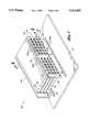
- FIG. 1is a perspective view illustrating a multi-chip memory module in accordance with a preferred embodiment of the present invention, illustrated above a portion of a printed circuit board to which the multi-chip memory module may be surface mounted. Solder plugs and circuit board traces are omitted to show the construction of the multi-chip memory module;
- FIG. 2is an exploded perspective view of the multi-chip memory module of FIG. 1;
- FIG. 3is a top plan view of the multi-chip memory module of FIG. 1, with terminal numbers for the multi-chip memory module shown in brackets;
- FIG. 4is a cross sectional view taken along the line 4--4 of FIG. 1;
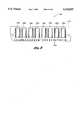
- FIGS. 5a and 5bare top and bottom plan views of a portion of a circuit board panel, illustrating a process of manufacturing side boards in accordance with the present invention, and further illustrating conductive traces on first and second sides of the side boards of FIG. 1;
- FIG. 6ais an enlarged view in partial cross section, showing a bottom portion of a side board of the multi-chip memory module of FIG. 1 with partially cut-away vias filled with solder to form surface mount terminals, and further showing the printed circuit board and pads of FIG. 1;
- FIG. 6bis an enlarged view in partial cross section of a side board and a printed circuit board with pads, illustrating an alternative configuration that results when conductive cylinders of vias are pushed inward during a routing process;
- FIG. 7is a schematic diagram illustrating the electrical interconnections of memory chip pins and side board terminals for the multi-chip memory module of FIG. 1, with chip pin numbers shown in parenthesis and multi-chip memory module terminal numbers shown in brackets; and
- FIG. 8is a plan view of a single in-line memory module having eight multi-chip memory modules surface mounted to one side thereof.
- one multi-chip memory module designis described herein.
- various embodiment-specific detailsare set forth, such as the number of memory chips in the module, the layouts of the printed circuit boards of the module, and the capacity, number of data bits and pin-outs of the memory chips. It should be understood, however, that these details are provided only to illustrate this single preferred embodiment, and are not intended to limit the scope of the present invention.
- a 28-terminal multi-chip memory module 30(hereinafter “multi-chip module”) comprises four functionally-identical, vertically-stacked memory chips 32, 34, 36, 38.
- the memory chips 32-38are conventional 24-pin surface mount TSOP ("thin small outline package") chips, available from Toshiba, Mitsubishi, and the like. Each memory chip 32-38 has a capacity of 16M ⁇ 1-bit.
- the vertically-stacked memory chips 32-38are held together and electrically interconnected by a pair of printed circuit boards 42, 44, referred to herein as "side boards.”
- the side boards 42, 44are positioned in parallel to each other, and perpendicular to the top surfaces of the chips 32-38.
- the multi-chip module 30is configured to be surface-mounted to a memory board 70 (FIG. 1) that has surface mount pads 66 thereon.
- bottomrefers generally to the portion of the multi-chip module 30 that is closest to the memory board 70 when the multi-chip module 30 is mounted to the memory board 70.
- toprefers generally to the portion of the multi-chip module 30 that is closest to the memory board 70 when the multi-chip module 30 is mounted to the memory board 70.
- bottomrefers generally to the portion of the multi-chip module 30 that is closest to the memory board 70 when the multi-chip module 30 is mounted to the memory board 70.
- topbottom
- lowerare not intended to imply a specific spacial orientation of the multi-chip module 30.
- Each side board 42, 44has a plurality of plated through-holes or "vias" 48 for receiving the pins 50 of the chips 32-38, with each via 48 comprising a conductive tubular cylinder portion 48a that extends through the side board.
- the vias 48are positioned to form four horizontal rows 52, 54, 56, 58, with each row corresponding to a respective memory chip 32, 34, 36, 38.
- the rows 52-58 of viasare formed such that the distance D between centers of adjacent rows is approximately equal to the thickness T of each chip 32-38, so that adjacent memory chips are touching (or nearly touching) each other when the multi-chip module 30 is assembled.
- Adjacent memory chipscould alternatively be spaced apart from one another, as may be desirable in certain applications to facilitate the cooling of the memory chips 32-38.
- the vias of the bottom-most row 58are partially cut away, with the conductive cylinder 48a of each such via extending to the lower edge 80 of the side board so that the pins 50 of the bottom-most chip 38 can be soldered directly to the surface mount pads 66 (FIG. 1) of the memory board 70.
- the vias 48 along the lower edges 80 of the side boards 42, 44thus serve as surface mount terminals.
- This aspect of the multi-chip module 30, in combination with the close spacings between adjacent memory chips,allows the multi-chip module 30 to be mounted with a very low profile relative to the memory board 70.
- the lower edge 80is preferably formed using a routing machine, as further described below.
- the multi-chip module 30has a total of 28 surface mount terminals (terminal numbers shown in brackets), with the terminals arranged in two rows of 14 terminals each.
- the surface mount pads 66are arranged in two rows of 14 pads each (corresponding to the 14 terminals per side board 42, 44), with the distance between the two rows corresponding to the width of each chip 32-38.
- the multi-chip module 30occupies approximately the same area on the memory board 70 as would a single one of the memory chips 32-38.
- the memory chips 32-38are interconnected such that all four 16M ⁇ 1-bit chips 32-38 are selected simultaneously, with each chip supplying (or, during a write cycle, storing) one bit of data.
- the multi-chip module 30thus acts as a 16M ⁇ 4-bit memory module.
- each via 72provides access to either a data input pin or a data output pin of a respective memory chip 32-38, and is thus dedicated to a single chip. It will be recognized that other types of terminal structures could be used in place of the vias 72.
- the memory chips 32-38are initially stacked on top of one another.
- the side boards 42, 44are then positioned so that the pins 50 extend within the corresponding vias, as best shown by FIG. 4.
- no modification to the pins 50 of the standard TSOP memory chips 32-38is required.
- all of the vias 48 of both side boards 42, 44are filled with solder (solder plugs omitted in FIGS. 1-4).
- a solder with a relatively high melting pointis used for this purpose so that the multi-chip module 30 can subsequently be mounted to the memory board 70 using a solder with a lower melting point without melting the solder within the vias 48.
- FIGS. 5a and 5billustrate a circuit board panel 90 mid-way through the manufacturing process.
- FIG. 5aillustrates the outward-facing surface (relative to the multi-chip module 30) of the side board 42, and the inward-facing surface of the side board 44.
- FIG. 5billustrates the inward-facing surface of the side board 42, and the outward-facing surface of the side board 44.
- Traces 92are initially formed on both sides of the circuit board panel 90 using a conventional film etching process. Via holes are then drilled through the circuit board panel 90, with the holes positioned to correspond to the pin positions of the chips 32-38. A conventional plating process is then used to form the conductive cylinders 48a of the vias 48 (preferably formed from copper), and to interconnect the via cylinders 48a to the appropriate traces 92.
- the panel 90is routed to form the lower edge 80 and the top edge 81 of each side board 42, 44.
- the panel 90 shown in FIGS. 5a and 5bis mid-way through the routing process, with top and bottom edges 80, 81 formed only for the four side boards 42, 44 closest to the bottom of each Figure.
- the routing bitis preferably passed so that approximately 5% of the diameter of each via cylinder 48a along the bottom row 58 is cut away. Due to imperfections in the routing process, the lower portions of some cylinders may be pushed inward (toward the centers of the respective vias) by the routing bit, as schematically shown at 96 in FIGS. 5a and 5b (and further illustrated in FIG. 6b). Cylinders that are formed in this manner have been found to work well as surface mount terminals, and need not be modified.
- the panel 90is scored on both sides to form break-away grooves 94.
- the break-away grooves 94can be formed either before or after the above-described routing process.
- side boards 42, 44are manually broken away from the panel 90, and soldered to stacks of memory chips (as described above) to form multi-chip modules 30.
- each solder plug 98is exposed along the bottom edge 80, forming a terminal that can be soldered to a corresponding surface mount pad 66.
- Each solder plug 98preferably extends slightly below the lower edge 80, facilitating connection of the multi-chip module 30 to the pads 66.
- via cylinders 48a that are pushed inward during the routing processare similarly exposed along the lower edge 80, and are well-suited for connection to the pads 66.
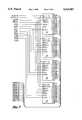
- FIG. 7illustrates the interconnections the memory chips 32-38 of the multi-chip module 30, and also illustrates the connections between the memory chips 32-38 and the 28 terminals of the multi-chip module 30.
- Signal names for each of the 28 multi-multi-chip module terminalsare shown at the left of FIG. 7.
- Terminal numbers for the multi-chip module 30are shown in brackets in FIG. 7, and correspond to the bracketed terminal numbers of FIG. 3.
- Pin numbers for the chips 32-38are shown in parenthesis in FIG. 6.
- like address pins (A0-A11), control pins (RAS, CAS and WE), and power pins (VCC and VSS) of the four memory chips 32-38are connected together, and are connected to respective terminals of the multi-chip module 30.
- the A0 pins (pin 8) of all four memory chips 32-38are connected together, and are accessed via terminal 10 of the multi-chip module. With like address and control pins connected together, all four chips 32-38 are selected simultaneously, and are fed identical address values.
- the data-input pin (D) of each memory chip 32-38is connected to a respective dedicated input terminal (D0-D3) of the multi-chip module 30, allowing a 4-bit value to be written to the multi-chip module 30 on each write cycle.
- the data-output pin (Q) of each memory chip 32-38is connected to a respective dedicated output terminal (Q0-Q3), allowing a 4-bit value to be read from to the multi-chip module 30 on each read cycle.
- the chips 32-38could alternatively be connected such that fewer than all of the chips are selected with each multi-chip module access.
- a 64M ⁇ 4-bit multi-chip modulecan be constructed from four 16M ⁇ 4-bit memory chips that are interconnected so that only one memory chip is selected at a time.
- the write enable pins and like address, data-in, and data-out pins of all four memory chipswould be connected, and the RAS and CAS pins of each chip would be connected to dedicated RAS and CAS input lines (i.e., one pair of RAS/CAS input lines per memory chip).
- FIG. 8illustrates one side of a 16M ⁇ 36 bit single in-line memory module (SIMM) 100 in accordance with the present invention.
- the SIMM 100comprises a SIMM board 170 having eight 16M ⁇ 4 bit multi-chip modules 30a-30h mounted on the side shown.
- Four 16M ⁇ 1-bit TSOP memory chips(not shown) are mounted on the opposite side of the SIMM board 170, in addition to one or more conventional buffer chips.
- Standard connector terminals 104are provided along the bottom edge of the SIMM 100, permitting insertion of the SIMM into a connector slot.
- the eight 16M ⁇ 4-bit multi-chip modules 30a-30h and four 16M ⁇ 1-bit memory chipscombine to produce a data width of 36 bits (32 data bits plus 4 error-correction code bits).
- the low profile of each multi-chip module 30a-30hadvantageously enables multiple SIMMs to be mounted in close proximity to one another within a computer.
- stacking techniques described hereinmay be useful in alternative applications that do not involve the stacking of memory chips.
- the stacking techniquescould be used to stack multiple buffer chips, or to stack multiple logic driver chips.
Landscapes
- Engineering & Computer Science (AREA)
- Microelectronics & Electronic Packaging (AREA)
- Power Engineering (AREA)
- Physics & Mathematics (AREA)
- Condensed Matter Physics & Semiconductors (AREA)
- General Physics & Mathematics (AREA)
- Computer Hardware Design (AREA)
- Dram (AREA)
Abstract
Description
1. Field of the Invention
The present invention relates to the vertical stacking of conventional integrated circuit packages to increase the density of components on a printed circuit board. More particularly, the present invention relates to the vertical stacking of conventional memory integrated circuits packages on a surface mount printed circuit board.
2. Description of the Related Art
An integrated circuit or "IC" is a microcircuit formed from active and passive electrical components interconnected on or within a single semiconductor substrate. To protect the IC and to facilitate connection of the IC to a printed circuit board, off-the-shelf ICs are commonly packaged within a ceramic, plastic or epoxy IC package having multiple external terminals or "pins." The full integrated circuit package, including the IC, is commonly referred to (and will be referred to herein) as a "chip."
As a result of the continuously increasing demand for large random access computer memories, and the demand for smaller computers, various techniques have been developed to increase densities of memory chips on printed circuit boards. In addition to the inherent size advantages provided, increased chip densities enable shorter circuit paths between components, allowing the components to operate at higher speeds while reducing radio-frequency interference (RFI) and electromagnetic interference (EMI) emitted from the printed circuit board.
One development that has led to a significant increase in memory chip densities has been the advent of surface mount technology. With surface mount technology, conventional plated through holes on printed circuit boards are replaced with conductive pads, and through-hole pins of conventional chips are replaced with smaller surface mount pins. Because the pitch or spacing between centers of adjacent surface mount pins is significantly less than the conventional 0.10-inch spacing for conventional through-hole components, surface mount chips tend to be considerably smaller than corresponding conventional chips, and thus take up less space on the printed circuit board. Surface mount technology additionally facilitates the mounting of components on both sides of the printed circuit board.
Various techniques have been developed for increasing chip densities on printed circuit boards by vertically stacking or "piggybacking" two or more chips. See, for example, U.S. Pat. No. 4,996,583 to Hatada, U.S. Pat. No. 4,398,235 to Lutz et al., U.S. Pat. No. 4,953,005 to Carlson et al., Japanese Patent Publication No. 61-63048 to Toshiba Corp., Japanese Patent Publication No. 58-219757 to Tokyo Shibaura Denki K. K., Japanese Patent Publication No. 61-75558 to NEC Corp., and Japanese Patent Publication No. 60-254762 to Fujitsu. These techniques, however, tend to suffer from a number of defects. For instance, many of the techniques require the manufacture of custom chips that are specifically designed for stacking, or else require special modifications to the pins of standard memory chips. Further, many of the techniques do not make use of the various advantages of surface mount technology, such as the ability to maintain a low-profile when memory chips are mounted to the printed circuit board. Further, many proposed techniques for stacking memory chips are not cost effective.
The present invention involves a multi-chip memory module having two or more vertically stacked memory chips that are interconnected using a pair of printed circuit boards or "side boards." The multi-chip memory module can be constructed using standard, off-the-shelf memory chips, without modification to the pins of the memory chips. The multi-chip memory module is constructed such that pins of the lower-most memory chip in the stack are surface-mountable directly to pads of a memory board, permitting the multi-chip memory module to be mounted with a low profile relative to the memory board.
In accordance with one aspect of the invention, the multi-chip memory module comprises a plurality of memory chips that are stacked on top of one another, with each memory chip having conductive surface mount pins. First and second side boards are mounted to the stacked memory chips such that the side boards are substantially parallel to one another. Each of the two side boards has vias for receiving the surface mount pins of the memory chips, with the vias arranged in rows such that each row corresponds to a respective memory chip. Vias of a bottom-most row of each side board fall along a lower side board edge, so that vias of the bottom-most row serve as surface mount terminals for surface mounting the multi-chip memory module to pads of a printed circuit board. Conductive traces are provided on or within each side board for interconnecting the surface mount pins of the memory chips.
In accordance with another aspect of the invention, there is provided a memory module that includes at least one multi-chip module. The memory module includes a circuit board having at least first and second sets of surface mount pads. The memory module further includes a first side board that is surface-mounted to the first set of surface mount pads such that the first side board is substantially perpendicular to the circuit board, and a second side board that is surface-mounted to the second set of surface mount pads such that the second side board is substantially perpendicular to the circuit board and substantially parallel to the first side board. The memory module further includes a plurality of chips stacked on top of one another between the side boards, with each chip conductively connected to the first and second side boards.
In accordance with an additional aspect of the invention, there is provided a method of increasing the density of memory chips on a memory board. The method includes the step of providing first and second side boards, with each side board comprising a printed circuit board having vias thereon, and with vias along bottom edges of the side boards forming surface mount terminals. The method further includes the step of stacking a plurality of memory chips on top of one another to generate a stack of memory chips. The method further includes the steps of positioning the first and second side boards relative to the stack of memory chips such that terminals of the memory chips extend within the vias, and attaching the first and second side boards to the stack of memory chips by filling the vias with solder.
In accordance with another aspect of the invention, there is provided a method of interconnecting circuit board components to increase component density. The method includes the step of constructing a first printed circuit board that has a plurality of vias formed along a row. The method further includes the step of cutting the first printed circuit board along the row to expose the vias along an edge of the printed circuit board. The method further includes the steps of soldering the vias to respective pins of a semiconductor chip, and soldering the vias to pads of a second printed circuit board such that the first printed circuit board is substantially perpendicular to the second printed circuit board.
These and other features of the invention will now be described with reference to the drawings of a preferred embodiment, which is intended to illustrate and not to limit the invention, and in which:
FIG. 1 is a perspective view illustrating a multi-chip memory module in accordance with a preferred embodiment of the present invention, illustrated above a portion of a printed circuit board to which the multi-chip memory module may be surface mounted. Solder plugs and circuit board traces are omitted to show the construction of the multi-chip memory module;
FIG. 2 is an exploded perspective view of the multi-chip memory module of FIG. 1;
FIG. 3 is a top plan view of the multi-chip memory module of FIG. 1, with terminal numbers for the multi-chip memory module shown in brackets;
FIG. 4 is a cross sectional view taken along theline 4--4 of FIG. 1;
FIGS. 5a and 5b are top and bottom plan views of a portion of a circuit board panel, illustrating a process of manufacturing side boards in accordance with the present invention, and further illustrating conductive traces on first and second sides of the side boards of FIG. 1;
FIG. 6a is an enlarged view in partial cross section, showing a bottom portion of a side board of the multi-chip memory module of FIG. 1 with partially cut-away vias filled with solder to form surface mount terminals, and further showing the printed circuit board and pads of FIG. 1;
FIG. 6b is an enlarged view in partial cross section of a side board and a printed circuit board with pads, illustrating an alternative configuration that results when conductive cylinders of vias are pushed inward during a routing process;
FIG. 7 is a schematic diagram illustrating the electrical interconnections of memory chip pins and side board terminals for the multi-chip memory module of FIG. 1, with chip pin numbers shown in parenthesis and multi-chip memory module terminal numbers shown in brackets; and
FIG. 8 is a plan view of a single in-line memory module having eight multi-chip memory modules surface mounted to one side thereof.
In accordance with one embodiment of the present invention, one multi-chip memory module design is described herein. In order to fully specify this preferred design, various embodiment-specific details are set forth, such as the number of memory chips in the module, the layouts of the printed circuit boards of the module, and the capacity, number of data bits and pin-outs of the memory chips. It should be understood, however, that these details are provided only to illustrate this single preferred embodiment, and are not intended to limit the scope of the present invention.
With reference to FIGS. 1-4, a 28-terminal multi-chip memory module 30 (hereinafter "multi-chip module") comprises four functionally-identical, vertically-stackedmemory chips
The vertically-stacked memory chips 32-38 are held together and electrically interconnected by a pair of printedcircuit boards side boards multi-chip module 30 is configured to be surface-mounted to a memory board 70 (FIG. 1) that hassurface mount pads 66 thereon.
As used herein to describe themulti-chip module 30, the term "bottom" refers generally to the portion of themulti-chip module 30 that is closest to thememory board 70 when themulti-chip module 30 is mounted to thememory board 70. The terms "top," "bottom," and "lower" are not intended to imply a specific spacial orientation of themulti-chip module 30.
Eachside board pins 50 of the chips 32-38, with each via 48 comprising a conductivetubular cylinder portion 48a that extends through the side board. Thevias 48 are positioned to form fourhorizontal rows respective memory chip multi-chip module 30 is assembled. This close spacing of adjacent memory chips contributes to a low profile of themulti-chip module 30 relative to the memory board 70 (FIG. 1), as further discussed below. Adjacent memory chips could alternatively be spaced apart from one another, as may be desirable in certain applications to facilitate the cooling of the memory chips 32-38.
With reference to FIGS. 1 and 2, for eachside board bottom-most row 58 are partially cut away, with theconductive cylinder 48a of each such via extending to thelower edge 80 of the side board so that thepins 50 of thebottom-most chip 38 can be soldered directly to the surface mount pads 66 (FIG. 1) of thememory board 70. Thevias 48 along thelower edges 80 of theside boards multi-chip module 30, in combination with the close spacings between adjacent memory chips, allows themulti-chip module 30 to be mounted with a very low profile relative to thememory board 70. Thelower edge 80 is preferably formed using a routing machine, as further described below. As illustrated in FIG. 3, themulti-chip module 30 has a total of 28 surface mount terminals (terminal numbers shown in brackets), with the terminals arranged in two rows of 14 terminals each.
With reference to FIG. 1, thesurface mount pads 66 are arranged in two rows of 14 pads each (corresponding to the 14 terminals perside board 42, 44), with the distance between the two rows corresponding to the width of each chip 32-38. As best seen in FIGS. 1 and 3, themulti-chip module 30 occupies approximately the same area on thememory board 70 as would a single one of the memory chips 32-38.
Conductive traces (shown in FIGS. 5a and 5b) of theside boards pins 50 of the memory chips 32-38 such that all memory locations of all memory chips 32-38 can be utilized. In the embodiment shown, the memory chips 32-38 are interconnected such that all four 16M×1-bit chips 32-38 are selected simultaneously, with each chip supplying (or, during a write cycle, storing) one bit of data. Themulti-chip module 30 thus acts as a 16M×4-bit memory module.
With reference to FIGS. 1-3, four "extra" vias 72 are provided along thelower edges 80 of themulti-chip module 30. The four vias 72 serve as terminals only, and do not receivepins 50 of any of the memory chips 32-38. Each via 72 provides access to either a data input pin or a data output pin of a respective memory chip 32-38, and is thus dedicated to a single chip. It will be recognized that other types of terminal structures could be used in place of thevias 72.
To assemble themulti-chip module 30, the memory chips 32-38 are initially stacked on top of one another. Theside boards pins 50 extend within the corresponding vias, as best shown by FIG. 4. Advantageously, no modification to thepins 50 of the standard TSOP memory chips 32-38 is required. Once theside boards vias 48 of bothside boards multi-chip module 30 can subsequently be mounted to thememory board 70 using a solder with a lower melting point without melting the solder within thevias 48.
A preferred process for manufacturing theside boards multi-chip module 30 will now be described with reference to FIGS. 5a and 5b, which illustrate acircuit board panel 90 mid-way through the manufacturing process. FIG. 5a illustrates the outward-facing surface (relative to the multi-chip module 30) of theside board 42, and the inward-facing surface of theside board 44. FIG. 5b illustrates the inward-facing surface of theside board 42, and the outward-facing surface of theside board 44.
Once thevias 48 and traces 92 are formed, thepanel 90 is routed to form thelower edge 80 and thetop edge 81 of eachside board panel 90 shown in FIGS. 5a and 5b is mid-way through the routing process, with top andbottom edges side boards cylinder 48a along thebottom row 58 is cut away. Due to imperfections in the routing process, the lower portions of some cylinders may be pushed inward (toward the centers of the respective vias) by the routing bit, as schematically shown at 96 in FIGS. 5a and 5b (and further illustrated in FIG. 6b). Cylinders that are formed in this manner have been found to work well as surface mount terminals, and need not be modified.
Thepanel 90 is scored on both sides to form break-awaygrooves 94. The break-awaygrooves 94 can be formed either before or after the above-described routing process. Finally,side boards panel 90, and soldered to stacks of memory chips (as described above) to formmulti-chip modules 30.
With reference to FIG. 6a, once the partially cut-away vias 48 along thebottom edge 80 of aside board solder plug 98 is exposed along thebottom edge 80, forming a terminal that can be soldered to a correspondingsurface mount pad 66. Each solder plug 98 preferably extends slightly below thelower edge 80, facilitating connection of themulti-chip module 30 to thepads 66. As illustrated in FIG. 6b, viacylinders 48a that are pushed inward during the routing process are similarly exposed along thelower edge 80, and are well-suited for connection to thepads 66.
FIG. 7 illustrates the interconnections the memory chips 32-38 of themulti-chip module 30, and also illustrates the connections between the memory chips 32-38 and the 28 terminals of themulti-chip module 30. Signal names for each of the 28 multi-multi-chip module terminals are shown at the left of FIG. 7. Terminal numbers for themulti-chip module 30 are shown in brackets in FIG. 7, and correspond to the bracketed terminal numbers of FIG. 3. Pin numbers for the chips 32-38 are shown in parenthesis in FIG. 6. As shown, like address pins (A0-A11), control pins (RAS, CAS and WE), and power pins (VCC and VSS) of the four memory chips 32-38 are connected together, and are connected to respective terminals of themulti-chip module 30. For example, the A0 pins (pin 8) of all four memory chips 32-38 are connected together, and are accessed viaterminal 10 of the multi-chip module. With like address and control pins connected together, all four chips 32-38 are selected simultaneously, and are fed identical address values. The data-input pin (D) of each memory chip 32-38 is connected to a respective dedicated input terminal (D0-D3) of themulti-chip module 30, allowing a 4-bit value to be written to themulti-chip module 30 on each write cycle. Similarly, the data-output pin (Q) of each memory chip 32-38 is connected to a respective dedicated output terminal (Q0-Q3), allowing a 4-bit value to be read from to themulti-chip module 30 on each read cycle. As will be recognized, the chips 32-38 could alternatively be connected such that fewer than all of the chips are selected with each multi-chip module access. For example, a 64M×4-bit multi-chip module can be constructed from four 16M×4-bit memory chips that are interconnected so that only one memory chip is selected at a time. In such an arrangement, the write enable pins and like address, data-in, and data-out pins of all four memory chips would be connected, and the RAS and CAS pins of each chip would be connected to dedicated RAS and CAS input lines (i.e., one pair of RAS/CAS input lines per memory chip).
FIG. 8 illustrates one side of a 16M×36 bit single in-line memory module (SIMM) 100 in accordance with the present invention. TheSIMM 100 comprises aSIMM board 170 having eight 16M×4 bitmulti-chip modules 30a-30h mounted on the side shown. Four 16M×1-bit TSOP memory chips (not shown) are mounted on the opposite side of theSIMM board 170, in addition to one or more conventional buffer chips.Standard connector terminals 104 are provided along the bottom edge of theSIMM 100, permitting insertion of the SIMM into a connector slot. The eight 16M×4-bitmulti-chip modules 30a-30h and four 16M×1-bit memory chips combine to produce a data width of 36 bits (32 data bits plus 4 error-correction code bits). The low profile of eachmulti-chip module 30a-30h advantageously enables multiple SIMMs to be mounted in close proximity to one another within a computer.
While the design of asingle multi-chip module 30 has been described in detail herein, various modifications to the design are possible without departing from the scope of the present invention. For example, a different type of memory chip can be used in the place of the 16M×1-bit chips 32-38 of themulti-chip module 30. Alternatively, a mixture of memory chips of different types can be used. Further, a different number of chips per multi-chip module can be used. Further, theside boards
It will further be noted that the stacking techniques described herein may be useful in alternative applications that do not involve the stacking of memory chips. For example, the stacking techniques could be used to stack multiple buffer chips, or to stack multiple logic driver chips.
Accordingly, the scope of the present invention is intended to be defined only by reference to the appended claims.
Claims (15)
1. A multi-chip memory module, comprising:
a plurality of memory chips stacked on top of one another, each memory chip of said plurality having conductive surface mount pins; and
first and second side boards mounted to said memory chips such that said side boards are substantially parallel to one another, each side board having:
vias for receiving said surface mount pins of said memory chips, said vias arranged in rows such that each row corresponds to a respective memory chip of said plurality, vias of a bottom-most row receiving surface mount pins of a bottom-most memory chip of said plurality, said bottom-most row falling along a lower side board edge such that vias of said bottom-most row serve as surface mount terminals for surface mounting the multi-chip memory module to pads of a printed circuit board; and
conductive traces for interconnecting said vias.
2. A multi-chip memory module as defined in claim 1, wherein said vias of said bottom-most row are exposed along said lower side board edge.
3. A multi-chip memory module as defined in claim 1, wherein all memory chips of said plurality are functionally identical.
4. A multi-chip memory module as defined in claim 1, wherein the total number of surface mount terminals on said first and second side boards is greater than the number of said surface mount pins on any one of said plurality memory chips.
5. A multi-chip memory module as defined in claim 1, wherein said memory chips of said plurality are interconnected by said traces such that all memory chips of said plurality are selected simultaneously.
6. A multi-chip memory module as defined in claim 1, in combination with a memory board having surface mount pads thereon, said vias of said bottom-most row soldered to said surface mount pads.
7. A module that includes at least one multi-chip module, said module comprising:
a circuit board having at least first and second sets of surface mount pads;
a first planar side board including a plurality of surface mount contacts positioned along an edge of said first side board which abuts said circuit board, said plurality of surface mount contacts of said first side board being surface-mounted to said first set of surface mount pads of said circuit board such that said first side board is substantially perpendicular to said circuit board;
a second planar side board including a plurality of surface mount contacts positioned along an edge of said second side board which abuts said circuit board, said plurality of surface mount contacts of said second side board being surface-mounted to said second set of surface mount pads of said circuit board such that said second side board is substantially perpendicular to said circuit board and substantially parallel to said first side board; and
a plurality of standard surface mount chips stacked between said side boards, each chip including a plurality of pins, a portion of each pin extending beyond a chip surface which lies generally parallel to said circuit board with said chip positioned between said side boards, each chip of said plurality conductively connected to said first side board and said second side board.
8. A module as defined in claim 7, wherein said first and second sets of surface mount pads are arranged in respective first and second rows.
9. A module as defined in claim 7, wherein a surface area of a region between said first and second side boards on said circuit board is generally equal to a surface area occupied by one of said chips of said plurality.
10. A module as defined in claim 7, wherein said standard surface mount chips of said plurality are stacked on top of one another.
11. A module as defined in claim 7, wherein all chips of said plurality are functionally identical.
12. A module as defined in claim 7, wherein a lower-most chip of said plurality is soldered to said first and second sets of surface mount pads.
13. A module as defined in claim 7, wherein each chip of said plurality is a memory chip.
14. A module as defined in claim 12, wherein said lower-most chip is additionally soldered to vias of said first and second side boards.
15. A module as defined in claim 14, wherein said lower-most chip is soldered to said vias with a first solder that has a first melting point, and is soldered to said first and second sets of surface mount pads with a second solder that has a second melting point, said second melting point lower than said first melting point.
Priority Applications (2)
| Application Number | Priority Date | Filing Date | Title |
|---|---|---|---|
| US08/408,552US5514907A (en) | 1995-03-21 | 1995-03-21 | Apparatus for stacking semiconductor chips |
| US09/064,348USRE36916E (en) | 1995-03-21 | 1998-04-22 | Apparatus for stacking semiconductor chips |
Applications Claiming Priority (1)
| Application Number | Priority Date | Filing Date | Title |
|---|---|---|---|
| US08/408,552US5514907A (en) | 1995-03-21 | 1995-03-21 | Apparatus for stacking semiconductor chips |
Related Child Applications (1)
| Application Number | Title | Priority Date | Filing Date |
|---|---|---|---|
| US09/064,348ReissueUSRE36916E (en) | 1995-03-21 | 1998-04-22 | Apparatus for stacking semiconductor chips |
Publications (1)
| Publication Number | Publication Date |
|---|---|
| US5514907Atrue US5514907A (en) | 1996-05-07 |
Family
ID=23616743
Family Applications (2)
| Application Number | Title | Priority Date | Filing Date |
|---|---|---|---|
| US08/408,552CeasedUS5514907A (en) | 1995-03-21 | 1995-03-21 | Apparatus for stacking semiconductor chips |
| US09/064,348Expired - LifetimeUSRE36916E (en) | 1995-03-21 | 1998-04-22 | Apparatus for stacking semiconductor chips |
Family Applications After (1)
| Application Number | Title | Priority Date | Filing Date |
|---|---|---|---|
| US09/064,348Expired - LifetimeUSRE36916E (en) | 1995-03-21 | 1998-04-22 | Apparatus for stacking semiconductor chips |
Country Status (1)
| Country | Link |
|---|---|
| US (2) | US5514907A (en) |
Cited By (133)
| Publication number | Priority date | Publication date | Assignee | Title |
|---|---|---|---|---|
| US5696031A (en)* | 1996-11-20 | 1997-12-09 | Micron Technology, Inc. | Device and method for stacking wire-bonded integrated circuit dice on flip-chip bonded integrated circuit dice |
| US5754405A (en)* | 1995-11-20 | 1998-05-19 | Mitsubishi Semiconductor America, Inc. | Stacked dual in-line package assembly |
| US5778522A (en)* | 1996-05-20 | 1998-07-14 | Staktek Corporation | Method of manufacturing a high density integrated circuit module with complex electrical interconnect rails having electrical interconnect strain relief |
| US5857858A (en)* | 1996-12-23 | 1999-01-12 | General Electric Company | Demountable and repairable low pitch interconnect for stacked multichip modules |
| US5963464A (en)* | 1998-02-26 | 1999-10-05 | International Business Machines Corporation | Stackable memory card |
| US6051887A (en)* | 1998-08-28 | 2000-04-18 | Medtronic, Inc. | Semiconductor stacked device for implantable medical apparatus |
| US6075284A (en)* | 1998-06-30 | 2000-06-13 | Hyundai Electronics Industries Co., Ltd. | Stack package |
| USRE36916E (en)* | 1995-03-21 | 2000-10-17 | Simple Technology Incorporated | Apparatus for stacking semiconductor chips |
| US6137162A (en)* | 1998-05-12 | 2000-10-24 | Hyundai Electronics Industries Co., Ltd. | Chip stack package |
| US6153929A (en)* | 1998-08-21 | 2000-11-28 | Micron Technology, Inc. | Low profile multi-IC package connector |
| US6163459A (en)* | 1997-07-25 | 2000-12-19 | Matsushita Electric Industrial Co., Ltd. | Semiconductor mounting system and semiconductor chip |
| US6183301B1 (en)* | 1997-01-16 | 2001-02-06 | Berg Technology, Inc. | Surface mount connector with integrated PCB assembly |
| US6190425B1 (en) | 1998-11-03 | 2001-02-20 | Zomaya Group, Inc. | Memory bar and related circuits and methods |
| US6222737B1 (en) | 1999-04-23 | 2001-04-24 | Dense-Pac Microsystems, Inc. | Universal package and method of forming the same |
| US20010005042A1 (en)* | 1992-12-11 | 2001-06-28 | Burns Carmen D. | Method of manufacturing a surface mount package |
| US6262895B1 (en) | 2000-01-13 | 2001-07-17 | John A. Forthun | Stackable chip package with flex carrier |
| US6281577B1 (en)* | 1996-06-28 | 2001-08-28 | Pac Tech-Packaging Technologies Gmbh | Chips arranged in plurality of planes and electrically connected to one another |
| US6295220B1 (en) | 1998-11-03 | 2001-09-25 | Zomaya Group, Inc. | Memory bar and related circuits and methods |
| US6316825B1 (en) | 1998-05-15 | 2001-11-13 | Hyundai Electronics Industries Co., Ltd. | Chip stack package utilizing a connecting hole to improve electrical connection between leadframes |
| US6329221B1 (en) | 1998-03-09 | 2001-12-11 | Micron Technology, Inc. | Method of forming a stack of packaged memory die and resulting apparatus |
| US6331938B1 (en)* | 1997-10-28 | 2001-12-18 | Surecom Technology Corporation | Structural and electrical connections for stacked computer devices |
| US6352437B1 (en)* | 1999-10-20 | 2002-03-05 | John O. Tate | Solder ball terminal |
| US20020045290A1 (en)* | 1996-02-20 | 2002-04-18 | Michael B. Ball | Flip chip and conventional stack |
| US6395578B1 (en) | 1999-05-20 | 2002-05-28 | Amkor Technology, Inc. | Semiconductor package and method for fabricating the same |
| US6404043B1 (en) | 2000-06-21 | 2002-06-11 | Dense-Pac Microsystems, Inc. | Panel stacking of BGA devices to form three-dimensional modules |
| US6409520B1 (en)* | 2001-07-31 | 2002-06-25 | Agilent Technologies, Inc. | Structure and method for interconnection of printed circuit boards |
| US6414396B1 (en) | 2000-01-24 | 2002-07-02 | Amkor Technology, Inc. | Package for stacked integrated circuits |
| US6426549B1 (en) | 1999-05-05 | 2002-07-30 | Harlan R. Isaak | Stackable flex circuit IC package and method of making same |
| US6437433B1 (en) | 2000-03-24 | 2002-08-20 | Andrew C. Ross | CSP stacking technology using rigid/flex construction |
| US6451626B1 (en) | 2001-07-27 | 2002-09-17 | Charles W.C. Lin | Three-dimensional stacked semiconductor package |
| US6452278B1 (en) | 2000-06-30 | 2002-09-17 | Amkor Technology, Inc. | Low profile package for plural semiconductor dies |
| US20020142515A1 (en)* | 2001-03-27 | 2002-10-03 | Staktek Group, L.P. | Contact member stacking system and method |
| US20020162215A1 (en)* | 2001-03-14 | 2002-11-07 | Kledzik Kenneth J. | Method and apparatus for fabricating a circuit board with a three dimensional surface mounted array of semiconductor chips |
| US6487078B2 (en) | 2000-03-13 | 2002-11-26 | Legacy Electronics, Inc. | Electronic module having a three dimensional array of carrier-mounted integrated circuit packages |
| US6486549B1 (en) | 2001-11-10 | 2002-11-26 | Bridge Semiconductor Corporation | Semiconductor module with encapsulant base |
| US20020190367A1 (en)* | 2001-06-15 | 2002-12-19 | Mantz Frank E. | Slice interconnect structure |
| US20030002267A1 (en)* | 2001-06-15 | 2003-01-02 | Mantz Frank E. | I/O interface structure |
| US20030040166A1 (en)* | 2001-05-25 | 2003-02-27 | Mark Moshayedi | Apparatus and method for stacking integrated circuits |
| US20030051911A1 (en)* | 2001-09-20 | 2003-03-20 | Roeters Glen E. | Post in ring interconnect using 3-D stacking |
| US6542376B1 (en)* | 2001-03-30 | 2003-04-01 | L-3 Communications Corporation | High density packaging of electronic components |
| US6542393B1 (en) | 2002-04-24 | 2003-04-01 | Ma Laboratories, Inc. | Dual-bank memory module with stacked DRAM chips having a concave-shaped re-route PCB in-between |
| US20030067082A1 (en)* | 2001-05-25 | 2003-04-10 | Mark Moshayedi | Apparatus and methods for stacking integrated circuit devices with interconnected stacking structure |
| US6552416B1 (en) | 2000-09-08 | 2003-04-22 | Amkor Technology, Inc. | Multiple die lead frame package with enhanced die-to-die interconnect routing using internal lead trace wiring |
| US20030081392A1 (en)* | 2001-10-26 | 2003-05-01 | Staktek Group, L.P. | Integrated circuit stacking system and method |
| US6573461B2 (en) | 2001-09-20 | 2003-06-03 | Dpac Technologies Corp | Retaining ring interconnect used for 3-D stacking |
| US6572387B2 (en) | 1999-09-24 | 2003-06-03 | Staktek Group, L.P. | Flexible circuit connector for stacked chip module |
| US6576992B1 (en) | 2001-10-26 | 2003-06-10 | Staktek Group L.P. | Chip scale stacking system and method |
| US6608763B1 (en) | 2000-09-15 | 2003-08-19 | Staktek Group L.P. | Stacking system and method |
| US20030165051A1 (en)* | 2000-03-13 | 2003-09-04 | Kledzik Kenneth J. | Modular integrated circuit chip carrier |
| US20030199118A1 (en)* | 1999-12-20 | 2003-10-23 | Amkor Technology, Inc. | Wire bonding method for a semiconductor package |
| US6660561B2 (en) | 2000-06-15 | 2003-12-09 | Dpac Technologies Corp. | Method of assembling a stackable integrated circuit chip |
| US20030232085A1 (en)* | 1999-01-08 | 2003-12-18 | Emisphere Technologies, Inc. | Polymeric delivery agents and delivery agent compounds |
| US20040000708A1 (en)* | 2001-10-26 | 2004-01-01 | Staktek Group, L.P. | Memory expansion and chip scale stacking system and method |
| US20040007771A1 (en)* | 1999-08-24 | 2004-01-15 | Amkor Technology, Inc. | Semiconductor package and method for fabricating the smae |
| WO2004012264A1 (en)* | 2002-07-25 | 2004-02-05 | Pulse Engineering, Inc. | High density electronics assembly and method |
| US6707684B1 (en) | 2001-04-02 | 2004-03-16 | Advanced Micro Devices, Inc. | Method and apparatus for direct connection between two integrated circuits via a connector |
| US20040052060A1 (en)* | 2001-10-26 | 2004-03-18 | Staktek Group, L.P. | Low profile chip scale stacking system and method |
| US6716670B1 (en) | 2002-01-09 | 2004-04-06 | Bridge Semiconductor Corporation | Method of forming a three-dimensional stacked semiconductor package device |
| US6717248B2 (en) | 1999-05-07 | 2004-04-06 | Amkor Technology, Inc. | Semiconductor package and method for fabricating the same |
| US6721196B1 (en)* | 1999-06-23 | 2004-04-13 | Giesecke & Devrient Gmbh | Semiconductor memory chip module |
| US20040108584A1 (en)* | 2002-12-05 | 2004-06-10 | Roeters Glen E. | Thin scale outline package |
| US20040124466A1 (en)* | 2002-12-31 | 2004-07-01 | Walker Andrew J. | Method for fabricating programmable memory array structures incorporating series-connected transistor strings |
| US20040125629A1 (en)* | 2002-12-31 | 2004-07-01 | Scheuerlein Roy E. | Programmable memory array structure incorporating series-connected transistor strings and methods for fabrication and operation of same |
| US6759737B2 (en) | 2000-03-25 | 2004-07-06 | Amkor Technology, Inc. | Semiconductor package including stacked chips with aligned input/output pads |
| US6762487B2 (en) | 2001-04-19 | 2004-07-13 | Simpletech, Inc. | Stack arrangements of chips and interconnecting members |
| US6765287B1 (en) | 2001-07-27 | 2004-07-20 | Charles W. C. Lin | Three-dimensional stacked semiconductor package |
| US20040145024A1 (en)* | 2002-12-31 | 2004-07-29 | En-Hsing Chen | NAND memory array incorporating capacitance boosting of channel regions in unselected memory cells and method for operation of same |
| US20040191442A1 (en)* | 2003-03-27 | 2004-09-30 | Florencia Lim | Surface modification of expanded ultra high molecular weight polyethylene (eUHMWPE) for improved bondability |
| US20040207990A1 (en)* | 2003-04-21 | 2004-10-21 | Rose Andrew C. | Stair-step signal routing |
| WO2004061861A3 (en)* | 2002-12-31 | 2004-10-28 | Matrix Semiconductor Inc | Nand memory array incorporating capacitance boosting of channel regions in unselected memory cells and method for operation of same |
| US20040245615A1 (en)* | 2003-06-03 | 2004-12-09 | Staktek Group, L.P. | Point to point memory expansion system and method |
| US20040252474A1 (en)* | 2002-11-25 | 2004-12-16 | Kwanghak Lee | Integrated circuit stack with lead frames |
| US20050009234A1 (en)* | 2001-10-26 | 2005-01-13 | Staktek Group, L.P. | Stacked module systems and methods for CSP packages |
| US20050018412A1 (en)* | 2001-10-26 | 2005-01-27 | Staktek Group, L.P. | Pitch change and chip scale stacking system |
| US6849480B1 (en) | 1999-05-07 | 2005-02-01 | Seagate Technology Llc | Surface mount IC stacking method and device |
| US6886076B1 (en)* | 1999-04-28 | 2005-04-26 | Sharp Kabushiki Kaisha | Semiconductor integrated circuit device having connection pads for superposing expansion memory |
| US20050098873A1 (en)* | 2003-09-15 | 2005-05-12 | Staktek Group L.P. | Stacked module systems and methods |
| US20050122779A1 (en)* | 2003-12-05 | 2005-06-09 | Fasoli Luca G. | Memory array incorporating memory cells arranged in NAND strings |
| US20050122780A1 (en)* | 2003-12-05 | 2005-06-09 | En-Hsing Chen | NAND memory array incorporating multiple write pulse programming of individual memory cells and method for operation of same |
| US20050128807A1 (en)* | 2003-12-05 | 2005-06-16 | En-Hsing Chen | Nand memory array incorporating multiple series selection devices and method for operation of same |
| US20050146031A1 (en)* | 2001-10-26 | 2005-07-07 | Staktek Group, L.P. | Low profile stacking system and method |
| US20050180120A1 (en)* | 2004-02-13 | 2005-08-18 | Levi Robert W. | Compact navigation device assembly |
| US20060006516A1 (en)* | 2004-07-09 | 2006-01-12 | Elpida Memory, Inc | Stacked semiconductor device and semiconductor memory module |
| US20060033187A1 (en)* | 2004-08-12 | 2006-02-16 | Staktek Group, L.P. | Rugged CSP module system and method |
| US7009296B1 (en) | 2004-01-15 | 2006-03-07 | Amkor Technology, Inc. | Semiconductor package with substrate coupled to a peripheral side surface of a semiconductor die |
| US7033861B1 (en) | 2005-05-18 | 2006-04-25 | Staktek Group L.P. | Stacked module systems and method |
| US20060107524A1 (en)* | 2000-10-16 | 2006-05-25 | Jason Engle | Method and apparatus for fabricating a circuit board with a three dimensional surface mounted array of semiconductor chips |
| US7067911B1 (en) | 2000-10-13 | 2006-06-27 | Bridge Semiconductor Corporation | Three-dimensional stacked semiconductor package with metal pillar in encapsulant aperture |
| US20060157842A1 (en)* | 2005-01-20 | 2006-07-20 | Staktek Group L.P. | Inverted CSP stacking system and method |
| US7081373B2 (en) | 2001-12-14 | 2006-07-25 | Staktek Group, L.P. | CSP chip stack with flex circuit |
| US20060164820A1 (en)* | 2005-01-12 | 2006-07-27 | Mecker Donald W | Radial circuit board, system, and methods |
| US20060170090A1 (en)* | 2005-01-31 | 2006-08-03 | Spansion Llc | Stacked type semiconductor device and method of fabricating stacked type semiconductor device |
| US7129113B1 (en) | 2000-10-13 | 2006-10-31 | Bridge Semiconductor Corporation | Method of making a three-dimensional stacked semiconductor package with a metal pillar in an encapsulant aperture |
| US7190060B1 (en) | 2002-01-09 | 2007-03-13 | Bridge Semiconductor Corporation | Three-dimensional stacked semiconductor package device with bent and flat leads and method of making same |
| US7202555B2 (en) | 2001-10-26 | 2007-04-10 | Staktek Group L.P. | Pitch change and chip scale stacking system and method |
| US7227249B1 (en) | 2003-12-24 | 2007-06-05 | Bridge Semiconductor Corporation | Three-dimensional stacked semiconductor package with chips on opposite sides of lead |
| US7262082B1 (en) | 2000-10-13 | 2007-08-28 | Bridge Semiconductor Corporation | Method of making a three-dimensional stacked semiconductor package with a metal pillar and a conductive interconnect in an encapsulant aperture |
| US7304382B2 (en) | 2006-01-11 | 2007-12-04 | Staktek Group L.P. | Managed memory component |
| US20070290312A1 (en)* | 2006-06-14 | 2007-12-20 | Staktek Group L.P. | Carrier structure stacking system and method |
| US20070290313A1 (en)* | 2006-06-14 | 2007-12-20 | Staktek Group L.P. | Interposer stacking system and method |
| USRE40112E1 (en) | 1999-05-20 | 2008-02-26 | Amkor Technology, Inc. | Semiconductor package and method for fabricating the same |
| US7371609B2 (en) | 2001-10-26 | 2008-05-13 | Staktek Group L.P. | Stacked module systems and methods |
| US7405471B2 (en) | 2000-10-16 | 2008-07-29 | Legacy Electronics, Inc. | Carrier-based electronic module |
| US20080203552A1 (en)* | 2005-02-15 | 2008-08-28 | Unisemicon Co., Ltd. | Stacked Package and Method of Fabricating the Same |
| US7468553B2 (en) | 2006-10-20 | 2008-12-23 | Entorian Technologies, Lp | Stackable micropackages and stacked modules |
| US7485951B2 (en) | 2001-10-26 | 2009-02-03 | Entorian Technologies, Lp | Modularized die stacking system and method |
| US7494843B1 (en) | 2006-12-26 | 2009-02-24 | Bridge Semiconductor Corporation | Method of making a semiconductor chip assembly with thermal conductor and encapsulant grinding |
| US7508058B2 (en) | 2006-01-11 | 2009-03-24 | Entorian Technologies, Lp | Stacked integrated circuit module |
| US7508069B2 (en) | 2006-01-11 | 2009-03-24 | Entorian Technologies, Lp | Managed memory component |
| US7576995B2 (en) | 2005-11-04 | 2009-08-18 | Entorian Technologies, Lp | Flex circuit apparatus and method for adding capacitance while conserving circuit board surface area |
| US7595550B2 (en) | 2001-10-26 | 2009-09-29 | Entorian Technologies, Lp | Flex-based circuit module |
| US7605454B2 (en) | 2006-01-11 | 2009-10-20 | Entorian Technologies, Lp | Memory card and method for devising |
| US7608920B2 (en) | 2006-01-11 | 2009-10-27 | Entorian Technologies, Lp | Memory card and method for devising |
| US20090267220A1 (en)* | 2008-04-23 | 2009-10-29 | Kuhlman Mark A | 3-d stacking of active devices over passive devices |
| US7656678B2 (en) | 2001-10-26 | 2010-02-02 | Entorian Technologies, Lp | Stacked module systems |
| US7811863B1 (en) | 2006-10-26 | 2010-10-12 | Bridge Semiconductor Corporation | Method of making a semiconductor chip assembly with metal pillar and encapsulant grinding and heat sink attachment |
| US7993983B1 (en) | 2003-11-17 | 2011-08-09 | Bridge Semiconductor Corporation | Method of making a semiconductor chip assembly with chip and encapsulant grinding |
| USD668659S1 (en)* | 2011-11-15 | 2012-10-09 | Connectblue Ab | Module |
| USD668658S1 (en)* | 2011-11-15 | 2012-10-09 | Connectblue Ab | Module |
| USD680119S1 (en)* | 2011-11-15 | 2013-04-16 | Connectblue Ab | Module |
| USD680545S1 (en)* | 2011-11-15 | 2013-04-23 | Connectblue Ab | Module |
| USD689053S1 (en)* | 2011-11-15 | 2013-09-03 | Connectblue Ab | Module |
| USD692896S1 (en)* | 2011-11-15 | 2013-11-05 | Connectblue Ab | Module |
| US9466545B1 (en) | 2007-02-21 | 2016-10-11 | Amkor Technology, Inc. | Semiconductor package in package |
| CN109411366A (en)* | 2018-09-17 | 2019-03-01 | 珠海欧比特电子有限公司 | A kind of 3 D stereo packaging method of surface protection |
| CN110054143A (en)* | 2019-04-30 | 2019-07-26 | 西安微电子技术研究所 | A kind of miniaturization anti high overload silicon substrate microsystem device and its assemble method |
| US10624225B1 (en)* | 2018-09-21 | 2020-04-14 | Aidenki Co., Ltd. | Electronic circuit holder |
| CN111511108A (en)* | 2019-01-31 | 2020-08-07 | 华为技术有限公司 | A circuit board assembly, terminal |
| US11272618B2 (en) | 2016-04-26 | 2022-03-08 | Analog Devices International Unlimited Company | Mechanically-compliant and electrically and thermally conductive leadframes for component-on-package circuits |
| US11410977B2 (en) | 2018-11-13 | 2022-08-09 | Analog Devices International Unlimited Company | Electronic module for high power applications |
| US11749576B2 (en) | 2018-03-27 | 2023-09-05 | Analog Devices International Unlimited Company | Stacked circuit package with molded base having laser drilled openings for upper package |
| US11844178B2 (en) | 2020-06-02 | 2023-12-12 | Analog Devices International Unlimited Company | Electronic component |
| US11894342B2 (en)* | 2008-09-06 | 2024-02-06 | Broadpak Corporation | Stacking integrated circuits containing serializer and deserializer blocks using through |
Families Citing this family (39)
| Publication number | Priority date | Publication date | Assignee | Title |
|---|---|---|---|---|
| US6278616B1 (en)* | 1998-07-07 | 2001-08-21 | Texas Instruments Incorporated | Modifying memory device organization in high density packages |
| JP2001352035A (en)* | 2000-06-07 | 2001-12-21 | Sony Corp | Assembling jig for multilayer semiconductor device and manufacturing method therefor |
| US20040096812A1 (en)* | 2001-01-02 | 2004-05-20 | Myers Dawes Andras ?amp; Sherman LLP Andras Joseph C. | Breadboard used for educational purposes |
| JP2002305286A (en)* | 2001-02-01 | 2002-10-18 | Mitsubishi Electric Corp | Semiconductor modules and electronic components |
| US6734538B1 (en) | 2001-04-12 | 2004-05-11 | Bae Systems Information & Electronic Systems Integration, Inc. | Article comprising a multi-layer electronic package and method therefor |
| US6433413B1 (en) | 2001-08-17 | 2002-08-13 | Micron Technology, Inc. | Three-dimensional multichip module |
| US6747347B2 (en) | 2001-08-30 | 2004-06-08 | Micron Technology, Inc. | Multi-chip electronic package and cooling system |
| US6635960B2 (en) | 2001-08-30 | 2003-10-21 | Micron Technology, Inc. | Angled edge connections for multichip structures |
| US6686654B2 (en) | 2001-08-31 | 2004-02-03 | Micron Technology, Inc. | Multiple chip stack structure and cooling system |
| US20060255446A1 (en) | 2001-10-26 | 2006-11-16 | Staktek Group, L.P. | Stacked modules and method |
| US7310458B2 (en) | 2001-10-26 | 2007-12-18 | Staktek Group L.P. | Stacked module systems and methods |
| JP2003188488A (en)* | 2001-12-19 | 2003-07-04 | Sumitomo Electric Ind Ltd | Electric circuit unit |
| TW586253B (en)* | 2003-04-25 | 2004-05-01 | Quanta Comp Inc | A PCB joint structure and manufacturing method thereof |
| US7612443B1 (en) | 2003-09-04 | 2009-11-03 | University Of Notre Dame Du Lac | Inter-chip communication |
| US7542304B2 (en) | 2003-09-15 | 2009-06-02 | Entorian Technologies, Lp | Memory expansion and integrated circuit stacking system and method |
| US7579687B2 (en) | 2004-09-03 | 2009-08-25 | Entorian Technologies, Lp | Circuit module turbulence enhancement systems and methods |
| US20060050492A1 (en) | 2004-09-03 | 2006-03-09 | Staktek Group, L.P. | Thin module system and method |
| US7606050B2 (en) | 2004-09-03 | 2009-10-20 | Entorian Technologies, Lp | Compact module system and method |
| US7324352B2 (en) | 2004-09-03 | 2008-01-29 | Staktek Group L.P. | High capacity thin module system and method |
| US7423885B2 (en) | 2004-09-03 | 2008-09-09 | Entorian Technologies, Lp | Die module system |
| US7289327B2 (en) | 2006-02-27 | 2007-10-30 | Stakick Group L.P. | Active cooling methods and apparatus for modules |
| US7542297B2 (en) | 2004-09-03 | 2009-06-02 | Entorian Technologies, Lp | Optimized mounting area circuit module system and method |
| US7511968B2 (en) | 2004-09-03 | 2009-03-31 | Entorian Technologies, Lp | Buffered thin module system and method |
| US7443023B2 (en) | 2004-09-03 | 2008-10-28 | Entorian Technologies, Lp | High capacity thin module system |
| US7606040B2 (en) | 2004-09-03 | 2009-10-20 | Entorian Technologies, Lp | Memory module system and method |
| US7522421B2 (en) | 2004-09-03 | 2009-04-21 | Entorian Technologies, Lp | Split core circuit module |
| US7468893B2 (en) | 2004-09-03 | 2008-12-23 | Entorian Technologies, Lp | Thin module system and method |
| US7446410B2 (en) | 2004-09-03 | 2008-11-04 | Entorian Technologies, Lp | Circuit module with thermal casing systems |
| US7606049B2 (en) | 2004-09-03 | 2009-10-20 | Entorian Technologies, Lp | Module thermal management system and method |
| US7616452B2 (en) | 2004-09-03 | 2009-11-10 | Entorian Technologies, Lp | Flex circuit constructions for high capacity circuit module systems and methods |
| US7760513B2 (en) | 2004-09-03 | 2010-07-20 | Entorian Technologies Lp | Modified core for circuit module system and method |
| JP4237160B2 (en)* | 2005-04-08 | 2009-03-11 | エルピーダメモリ株式会社 | Multilayer semiconductor device |
| US7511969B2 (en) | 2006-02-02 | 2009-03-31 | Entorian Technologies, Lp | Composite core circuit module system and method |
| US7928549B2 (en)* | 2006-09-19 | 2011-04-19 | Taiwan Semiconductor Manufacturing Co., Ltd. | Integrated circuit devices with multi-dimensional pad structures |
| US7417310B2 (en) | 2006-11-02 | 2008-08-26 | Entorian Technologies, Lp | Circuit module having force resistant construction |
| US7539034B2 (en)* | 2007-02-01 | 2009-05-26 | Qimonda North America Corp. | Memory configured on a common substrate |
| US8194411B2 (en)* | 2009-03-31 | 2012-06-05 | Hong Kong Applied Science and Technology Research Institute Co. Ltd | Electronic package with stacked modules with channels passing through metal layers of the modules |
| US8236610B2 (en) | 2009-05-26 | 2012-08-07 | International Business Machines Corporation | Forming semiconductor chip connections |
| US9620473B1 (en) | 2013-01-18 | 2017-04-11 | University Of Notre Dame Du Lac | Quilt packaging system with interdigitated interconnecting nodules for inter-chip alignment |
Citations (43)
| Publication number | Priority date | Publication date | Assignee | Title |
|---|---|---|---|---|
| US3246386A (en)* | 1962-01-26 | 1966-04-19 | Corning Glass Works | Electrical connected component and method |
| US3290559A (en)* | 1964-06-16 | 1966-12-06 | Internat Energy Conversion Inc | Modular assembly for functional electronic blocks |
| US3313986A (en)* | 1959-05-06 | 1967-04-11 | Texas Instruments Inc | Interconnecting miniature circuit modules |
| US3377516A (en)* | 1966-08-04 | 1968-04-09 | Hughes Aircraft Co | Cordwood package with removable plugs |
| US3403300A (en)* | 1966-09-01 | 1968-09-24 | Magnavox Co | Electronic module |
| US3515949A (en)* | 1967-11-22 | 1970-06-02 | Bunker Ramo | 3-d flatpack module packaging technique |
| US3535595A (en)* | 1967-11-09 | 1970-10-20 | Ferroxcube Corp | Universal cord-wood module |
| US3614541A (en)* | 1969-04-08 | 1971-10-19 | North American Rockwell | Package for an electronic assembly |
| US3671812A (en)* | 1970-07-01 | 1972-06-20 | Martin Marietta Corp | High density packaging of electronic components in three-dimensional modules |
| US3949274A (en)* | 1974-05-30 | 1976-04-06 | International Business Machines Corporation | Packaging and interconnection for superconductive circuitry |
| US4017963A (en)* | 1973-02-26 | 1977-04-19 | Signetics Corporation | Semiconductor assembly and method |
| US4288841A (en)* | 1979-09-20 | 1981-09-08 | Bell Telephone Laboratories, Incorporated | Double cavity semiconductor chip carrier |
| US4394712A (en)* | 1981-03-18 | 1983-07-19 | General Electric Company | Alignment-enhancing feed-through conductors for stackable silicon-on-sapphire wafers |
| US4398235A (en)* | 1980-09-11 | 1983-08-09 | General Motors Corporation | Vertical integrated circuit package integration |
| JPS58219757A (en)* | 1982-06-16 | 1983-12-21 | Toshiba Corp | Semiconductor device |
| JPS60160664A (en)* | 1984-01-31 | 1985-08-22 | Fujitsu Ltd | Manufacturing method of semiconductor device |
| JPS60254762A (en)* | 1984-05-31 | 1985-12-16 | Fujitsu Ltd | Semiconductor device package |
| JPS6163048A (en)* | 1984-09-04 | 1986-04-01 | Toshiba Corp | memory module |
| JPS6175558A (en)* | 1984-09-21 | 1986-04-17 | Nec Corp | Hybrid integrated circuit device |
| US4631573A (en)* | 1985-05-24 | 1986-12-23 | Sundstrand Corporation | Cooled stack of electrically isolated semiconductors |
| US4638406A (en)* | 1984-10-04 | 1987-01-20 | Motorola, Inc. | Discrete component mounting assembly |
| US4642735A (en)* | 1984-02-27 | 1987-02-10 | General Electric Company | Frequency synthesizer module |
| US4698663A (en)* | 1986-09-17 | 1987-10-06 | Fujitsu Limited | Heatsink package for flip-chip IC |
| US4706166A (en)* | 1986-04-25 | 1987-11-10 | Irvine Sensors Corporation | High-density electronic modules--process and product |
| US4821007A (en)* | 1987-02-06 | 1989-04-11 | Tektronix, Inc. | Strip line circuit component and method of manufacture |
| US4924352A (en)* | 1987-12-22 | 1990-05-08 | Societe Anonyme Dite: Alcatel Cit | Method and device for cooling an integrated circuit package |
| US4953005A (en)* | 1987-04-17 | 1990-08-28 | Xoc Devices, Inc. | Packaging system for stacking integrated circuits |
| FR2645681A1 (en)* | 1989-04-07 | 1990-10-12 | Thomson Csf | Vertical interconnection device for integrated-circuit chips and its method of manufacture |
| JPH02260448A (en)* | 1989-03-30 | 1990-10-23 | Mitsubishi Electric Corp | Semiconductor device and radiating fin |
| US4996583A (en)* | 1989-02-15 | 1991-02-26 | Matsushita Electric Industrial Co., Ltd. | Stack type semiconductor package |
| US4996587A (en)* | 1989-04-10 | 1991-02-26 | International Business Machines Corporation | Integrated semiconductor chip package |
| JPH0396266A (en)* | 1989-09-08 | 1991-04-22 | Mitsubishi Electric Corp | Semiconductor integrated circuit module |
| US5016138A (en)* | 1987-10-27 | 1991-05-14 | Woodman John K | Three dimensional integrated circuit package |
| US5043794A (en)* | 1990-09-24 | 1991-08-27 | At&T Bell Laboratories | Integrated circuit package and compact assemblies thereof |
| US5058265A (en)* | 1990-05-10 | 1991-10-22 | Rockwell International Corporation | Method for packaging a board of electronic components |
| US5128831A (en)* | 1991-10-31 | 1992-07-07 | Micron Technology, Inc. | High-density electronic package comprising stacked sub-modules which are electrically interconnected by solder-filled vias |
| JPH04209562A (en)* | 1990-12-06 | 1992-07-30 | Fujitsu Ltd | Module structure of semiconductor package |
| US5140745A (en)* | 1990-07-23 | 1992-08-25 | Mckenzie Jr Joseph A | Method for forming traces on side edges of printed circuit boards and devices formed thereby |
| US5198888A (en)* | 1987-12-28 | 1993-03-30 | Hitachi, Ltd. | Semiconductor stacked device |
| US5241454A (en)* | 1992-01-22 | 1993-08-31 | International Business Machines Corporation | Mutlilayered flexible circuit package |
| US5281852A (en)* | 1991-12-10 | 1994-01-25 | Normington Peter J C | Semiconductor device including stacked die |
| US5343366A (en)* | 1992-06-24 | 1994-08-30 | International Business Machines Corporation | Packages for stacked integrated circuit chip cubes |
| US5343075A (en)* | 1991-06-29 | 1994-08-30 | Sony Corporation | Composite stacked semiconductor device with contact plates |
Family Cites Families (46)
| Publication number | Priority date | Publication date | Assignee | Title |
|---|---|---|---|---|
| US3746934A (en)* | 1971-05-06 | 1973-07-17 | Siemens Ag | Stack arrangement of semiconductor chips |
| US3959579A (en)* | 1974-08-19 | 1976-05-25 | International Business Machines Corporation | Apertured semi-conductor device mounted on a substrate |
| US4116519A (en)* | 1977-08-02 | 1978-09-26 | Amp Incorporated | Electrical connections for chip carriers |
| US4116518A (en)* | 1977-08-31 | 1978-09-26 | Ncr Corporation | Clip for paralleling packaged integrated circuit chips |
| GB1553065A (en)* | 1978-01-28 | 1979-09-19 | Int Computers Ltd | Circuit structures including integrated circuits |
| US4379259A (en)* | 1980-03-12 | 1983-04-05 | National Semiconductor Corporation | Process of performing burn-in and parallel functional testing of integrated circuit memories in an environmental chamber |
| US4364620A (en)* | 1980-09-05 | 1982-12-21 | Mostek Corporation | Socket for housing a plurality of integrated circuits |
| US4371912A (en)* | 1980-10-01 | 1983-02-01 | Motorola, Inc. | Method of mounting interrelated components |
| GB2123216B (en)* | 1982-06-19 | 1985-12-18 | Ferranti Plc | Electrical circuit assemblies |
| EP0115514B1 (en)* | 1982-08-10 | 1986-11-12 | BROWN, David, Frank | Chip carrier |
| US4761681A (en)* | 1982-09-08 | 1988-08-02 | Texas Instruments Incorporated | Method for fabricating a semiconductor contact and interconnect structure using orientation dependent etching and thermomigration |
| US4574331A (en)* | 1983-05-31 | 1986-03-04 | Trw Inc. | Multi-element circuit construction |
| US4770640A (en)* | 1983-06-24 | 1988-09-13 | Walter Howard F | Electrical interconnection device for integrated circuits |
| JPS60160641A (en)* | 1984-01-31 | 1985-08-22 | Sharp Corp | Board mounting method for leadless package IC |
| JPS60194548A (en)* | 1984-03-16 | 1985-10-03 | Nec Corp | Chip carrier |
| KR890004820B1 (en)* | 1984-03-28 | 1989-11-27 | 인터내셔널 비지네스 머신즈 코포레이션 | Memory module and board with double storage density and method of forming the same |
| JPS61137335A (en)* | 1984-12-10 | 1986-06-25 | Toshiba Corp | Semiconductor device |
| FR2580136B1 (en)* | 1985-04-05 | 1988-10-14 | Radiotechnique Compelec | |
| US4696525A (en)* | 1985-12-13 | 1987-09-29 | Amp Incorporated | Socket for stacking integrated circuit packages |
| US5031072A (en)* | 1986-08-01 | 1991-07-09 | Texas Instruments Incorporated | Baseboard for orthogonal chip mount |
| US4868712A (en)* | 1987-02-04 | 1989-09-19 | Woodman John K | Three dimensional integrated circuit package |
| US4841355A (en)* | 1988-02-10 | 1989-06-20 | Amdahl Corporation | Three-dimensional microelectronic package for semiconductor chips |
| US4956694A (en)* | 1988-11-04 | 1990-09-11 | Dense-Pac Microsystems, Inc. | Integrated circuit chip stacking |
| FR2645680B1 (en)* | 1989-04-07 | 1994-04-29 | Thomson Microelectronics Sa Sg | ENCAPSULATION OF ELECTRONIC MODULES AND MANUFACTURING METHOD |
| US5231304A (en)* | 1989-07-27 | 1993-07-27 | Grumman Aerospace Corporation | Framed chip hybrid stacked layer assembly |
| US5155068A (en)* | 1989-08-31 | 1992-10-13 | Sharp Kabushiki Kaisha | Method for manufacturing an IC module for an IC card whereby an IC device and surrounding encapsulant are thinned by material removal |
| EP0509065A1 (en)* | 1990-08-01 | 1992-10-21 | Staktek Corporation | Ultra high density integrated circuit packages, method and apparatus |
| US5499160A (en)* | 1990-08-01 | 1996-03-12 | Staktek Corporation | High density integrated circuit module with snap-on rail assemblies |
| US5107328A (en)* | 1991-02-13 | 1992-04-21 | Micron Technology, Inc. | Packaging means for a semiconductor die having particular shelf structure |
| US5086018A (en)* | 1991-05-02 | 1992-02-04 | International Business Machines Corporation | Method of making a planarized thin film covered wire bonded semiconductor package |
| US5311401A (en)* | 1991-07-09 | 1994-05-10 | Hughes Aircraft Company | Stacked chip assembly and manufacturing method therefor |
| US5239447A (en)* | 1991-09-13 | 1993-08-24 | International Business Machines Corporation | Stepped electronic device package |
| JPH0715969B2 (en)* | 1991-09-30 | 1995-02-22 | インターナショナル・ビジネス・マシーンズ・コーポレイション | Multi-chip integrated circuit package and system thereof |
| US5397916A (en)* | 1991-12-10 | 1995-03-14 | Normington; Peter J. C. | Semiconductor device including stacked die |
| US5222014A (en)* | 1992-03-02 | 1993-06-22 | Motorola, Inc. | Three-dimensional multi-chip pad array carrier |
| US5313096A (en)* | 1992-03-16 | 1994-05-17 | Dense-Pac Microsystems, Inc. | IC chip package having chip attached to and wire bonded within an overlying substrate |
| MY109101A (en)* | 1992-05-25 | 1996-12-31 | Hitachi Ltd | Thin type semiconductor device, module structure using the device and method of mounting the device on board |
| FR2694840B1 (en)* | 1992-08-13 | 1994-09-09 | Commissariat Energie Atomique | Three-dimensional multi-chip module. |
| US5455740A (en)* | 1994-03-07 | 1995-10-03 | Staktek Corporation | Bus communication system for stacked high density integrated circuit packages |
| US5369056A (en)* | 1993-03-29 | 1994-11-29 | Staktek Corporation | Warp-resistent ultra-thin integrated circuit package fabrication method |
| JPH07122842A (en)* | 1993-10-25 | 1995-05-12 | Toshiba Corp | Printed wiring board |
| US5384689A (en)* | 1993-12-20 | 1995-01-24 | Shen; Ming-Tung | Integrated circuit chip including superimposed upper and lower printed circuit boards |
| US5380681A (en)* | 1994-03-21 | 1995-01-10 | United Microelectronics Corporation | Three-dimensional multichip package and methods of fabricating |
| US5615475A (en)* | 1995-01-30 | 1997-04-01 | Staktek Corporation | Method of manufacturing an integrated package having a pair of die on a common lead frame |
| US5514907A (en)* | 1995-03-21 | 1996-05-07 | Simple Technology Incorporated | Apparatus for stacking semiconductor chips |
| US5612570A (en)* | 1995-04-13 | 1997-03-18 | Dense-Pac Microsystems, Inc. | Chip stack and method of making same |
- 1995
- 1995-03-21USUS08/408,552patent/US5514907A/ennot_activeCeased
- 1998
- 1998-04-22USUS09/064,348patent/USRE36916E/ennot_activeExpired - Lifetime
Patent Citations (44)
| Publication number | Priority date | Publication date | Assignee | Title |
|---|---|---|---|---|
| US3313986A (en)* | 1959-05-06 | 1967-04-11 | Texas Instruments Inc | Interconnecting miniature circuit modules |
| US3246386A (en)* | 1962-01-26 | 1966-04-19 | Corning Glass Works | Electrical connected component and method |
| US3290559A (en)* | 1964-06-16 | 1966-12-06 | Internat Energy Conversion Inc | Modular assembly for functional electronic blocks |
| US3377516A (en)* | 1966-08-04 | 1968-04-09 | Hughes Aircraft Co | Cordwood package with removable plugs |
| US3403300A (en)* | 1966-09-01 | 1968-09-24 | Magnavox Co | Electronic module |
| US3535595A (en)* | 1967-11-09 | 1970-10-20 | Ferroxcube Corp | Universal cord-wood module |
| US3515949A (en)* | 1967-11-22 | 1970-06-02 | Bunker Ramo | 3-d flatpack module packaging technique |
| US3614541A (en)* | 1969-04-08 | 1971-10-19 | North American Rockwell | Package for an electronic assembly |
| US3671812A (en)* | 1970-07-01 | 1972-06-20 | Martin Marietta Corp | High density packaging of electronic components in three-dimensional modules |
| US4017963A (en)* | 1973-02-26 | 1977-04-19 | Signetics Corporation | Semiconductor assembly and method |
| US3949274A (en)* | 1974-05-30 | 1976-04-06 | International Business Machines Corporation | Packaging and interconnection for superconductive circuitry |
| US4288841A (en)* | 1979-09-20 | 1981-09-08 | Bell Telephone Laboratories, Incorporated | Double cavity semiconductor chip carrier |
| US4398235A (en)* | 1980-09-11 | 1983-08-09 | General Motors Corporation | Vertical integrated circuit package integration |
| US4394712A (en)* | 1981-03-18 | 1983-07-19 | General Electric Company | Alignment-enhancing feed-through conductors for stackable silicon-on-sapphire wafers |
| JPS58219757A (en)* | 1982-06-16 | 1983-12-21 | Toshiba Corp | Semiconductor device |
| JPS60160664A (en)* | 1984-01-31 | 1985-08-22 | Fujitsu Ltd | Manufacturing method of semiconductor device |
| US4642735A (en)* | 1984-02-27 | 1987-02-10 | General Electric Company | Frequency synthesizer module |
| JPS60254762A (en)* | 1984-05-31 | 1985-12-16 | Fujitsu Ltd | Semiconductor device package |
| JPS6163048A (en)* | 1984-09-04 | 1986-04-01 | Toshiba Corp | memory module |
| JPS6175558A (en)* | 1984-09-21 | 1986-04-17 | Nec Corp | Hybrid integrated circuit device |
| US4638406A (en)* | 1984-10-04 | 1987-01-20 | Motorola, Inc. | Discrete component mounting assembly |
| US4631573A (en)* | 1985-05-24 | 1986-12-23 | Sundstrand Corporation | Cooled stack of electrically isolated semiconductors |
| US4706166A (en)* | 1986-04-25 | 1987-11-10 | Irvine Sensors Corporation | High-density electronic modules--process and product |
| US4698663A (en)* | 1986-09-17 | 1987-10-06 | Fujitsu Limited | Heatsink package for flip-chip IC |
| US4821007A (en)* | 1987-02-06 | 1989-04-11 | Tektronix, Inc. | Strip line circuit component and method of manufacture |
| US4953005A (en)* | 1987-04-17 | 1990-08-28 | Xoc Devices, Inc. | Packaging system for stacking integrated circuits |
| US5016138A (en)* | 1987-10-27 | 1991-05-14 | Woodman John K | Three dimensional integrated circuit package |
| US4924352A (en)* | 1987-12-22 | 1990-05-08 | Societe Anonyme Dite: Alcatel Cit | Method and device for cooling an integrated circuit package |
| US5198888A (en)* | 1987-12-28 | 1993-03-30 | Hitachi, Ltd. | Semiconductor stacked device |
| US4996583A (en)* | 1989-02-15 | 1991-02-26 | Matsushita Electric Industrial Co., Ltd. | Stack type semiconductor package |
| JPH02260448A (en)* | 1989-03-30 | 1990-10-23 | Mitsubishi Electric Corp | Semiconductor device and radiating fin |
| US5025307A (en)* | 1989-03-30 | 1991-06-18 | Mitsubishi Denki Kabushiki Kaisha | Modular semiconductor device |
| FR2645681A1 (en)* | 1989-04-07 | 1990-10-12 | Thomson Csf | Vertical interconnection device for integrated-circuit chips and its method of manufacture |
| US4996587A (en)* | 1989-04-10 | 1991-02-26 | International Business Machines Corporation | Integrated semiconductor chip package |
| JPH0396266A (en)* | 1989-09-08 | 1991-04-22 | Mitsubishi Electric Corp | Semiconductor integrated circuit module |
| US5058265A (en)* | 1990-05-10 | 1991-10-22 | Rockwell International Corporation | Method for packaging a board of electronic components |
| US5140745A (en)* | 1990-07-23 | 1992-08-25 | Mckenzie Jr Joseph A | Method for forming traces on side edges of printed circuit boards and devices formed thereby |
| US5043794A (en)* | 1990-09-24 | 1991-08-27 | At&T Bell Laboratories | Integrated circuit package and compact assemblies thereof |
| JPH04209562A (en)* | 1990-12-06 | 1992-07-30 | Fujitsu Ltd | Module structure of semiconductor package |
| US5343075A (en)* | 1991-06-29 | 1994-08-30 | Sony Corporation | Composite stacked semiconductor device with contact plates |
| US5128831A (en)* | 1991-10-31 | 1992-07-07 | Micron Technology, Inc. | High-density electronic package comprising stacked sub-modules which are electrically interconnected by solder-filled vias |
| US5281852A (en)* | 1991-12-10 | 1994-01-25 | Normington Peter J C | Semiconductor device including stacked die |
| US5241454A (en)* | 1992-01-22 | 1993-08-31 | International Business Machines Corporation | Mutlilayered flexible circuit package |
| US5343366A (en)* | 1992-06-24 | 1994-08-30 | International Business Machines Corporation | Packages for stacked integrated circuit chip cubes |
Non-Patent Citations (12)
| Title |
|---|
| 1992 Proceedings. 42nd Electronic Components & Technology Conference. May 18 20, 1992.* |
| 1992 Proceedings. 42nd Electronic Components & Technology Conference. May 18-20, 1992. |
| 3 D Integrated packaging and Interconnect Technology; Wescon/90 Conference Record, held 13 15 Nov. 1990, Anaheim, Ca.* |
| 3-D Integrated packaging and Interconnect Technology; Wescon/90 Conference Record, held 13-15 Nov. 1990, Anaheim, Ca. |
| Article/Laminated Memory: A New 3 Dimensional Packaging Technology for MCMs. nCHIP, Inc., 1971 N. Capitol Avenue, San Jose, CA 95132 USA.* |
| Dense Pac Microsystems flyer/ While others are still defining it . . . Our customers are cashing in .* |
| Dense Pac Microsystems; 16 Megabit high Speed CMOS SRAM.* |
| Dense-Pac Microsystems flyer/"While others are still defining it . . . Our customers are cashing in". |
| Dense-Pac Microsystems; 16 Megabit high Speed CMOS SRAM. |
| IBM Technical Disclosure Bulletin, vol. 23 No. 12 May 1981.* |
| IBM Technical Disclosure Bulletin. Vo. 32. No. 3B Aug. 1989.* |
| IBM Technical Disclosure Bulletin. vol. 20 No. 11A Apr. 1978.* |
Cited By (260)
| Publication number | Priority date | Publication date | Assignee | Title |
|---|---|---|---|---|
| US20010005042A1 (en)* | 1992-12-11 | 2001-06-28 | Burns Carmen D. | Method of manufacturing a surface mount package |
| US6919626B2 (en) | 1992-12-11 | 2005-07-19 | Staktek Group L.P. | High density integrated circuit module |
| USRE36916E (en)* | 1995-03-21 | 2000-10-17 | Simple Technology Incorporated | Apparatus for stacking semiconductor chips |
| US5754405A (en)* | 1995-11-20 | 1998-05-19 | Mitsubishi Semiconductor America, Inc. | Stacked dual in-line package assembly |
| US7166495B2 (en) | 1996-02-20 | 2007-01-23 | Micron Technology, Inc. | Method of fabricating a multi-die semiconductor package assembly |
| US20020045290A1 (en)* | 1996-02-20 | 2002-04-18 | Michael B. Ball | Flip chip and conventional stack |
| US6140149A (en)* | 1996-02-20 | 2000-10-31 | Micron Technology, Inc. | Device and method for stacking wire-bonded integrated circuit dice on flip-chip bonded integrated circuit dice |
| US20070117266A1 (en)* | 1996-02-20 | 2007-05-24 | Ball Michael B | Method of fabricating a multi-die semiconductor package assembly |
| US5960539A (en)* | 1996-05-20 | 1999-10-05 | Staktek Corporation | Method of making high density integrated circuit module |
| US6288907B1 (en) | 1996-05-20 | 2001-09-11 | Staktek Group, L.P. | High density integrated circuit module with complex electrical interconnect rails having electrical interconnect strain relief |
| US5778522A (en)* | 1996-05-20 | 1998-07-14 | Staktek Corporation | Method of manufacturing a high density integrated circuit module with complex electrical interconnect rails having electrical interconnect strain relief |
| US7087442B2 (en)* | 1996-06-28 | 2006-08-08 | Pac Tech-Packaging Technologies Gmbh | Process for the formation of a spatial chip arrangement and spatial chip arrangement |
| US20020009828A1 (en)* | 1996-06-28 | 2002-01-24 | Pac Tech - Packaging Technologies Gmbh | Process for the formation of a spatial chip arrangement and spatial chip arrangement |
| US6281577B1 (en)* | 1996-06-28 | 2001-08-28 | Pac Tech-Packaging Technologies Gmbh | Chips arranged in plurality of planes and electrically connected to one another |
| US6605489B2 (en) | 1996-11-20 | 2003-08-12 | Micron Technology, Inc. | Methods for stacking wire-bonded integrated circuit dice on flip-chip bonded integrated circuit dice |
| US20080311702A1 (en)* | 1996-11-20 | 2008-12-18 | Micron Technology, Inc. | Methods for stacking wire-bonded integrated circuit dice on flip-chip bonded integrated circuit dice |
| US20070063327A1 (en)* | 1996-11-20 | 2007-03-22 | Wark James M | Methods for stacking wire-bonded integrated circuit dice on flip-chip bonded integrated circuit dice |
| US7423338B2 (en) | 1996-11-20 | 2008-09-09 | Micron Technology, Inc. | Methods for stacking wire-bonded integrated circuit dice on flip-chip bonded integrated circuit dice |
| US7776652B2 (en) | 1996-11-20 | 2010-08-17 | Micron Technology, Inc. | Methods for stacking wire-bonded integrated circuit dice on flip-chip bonded integrated circuit dice |
| US20040029315A1 (en)* | 1996-11-20 | 2004-02-12 | Wark James M. | Methods for stacking wire-bonded integrated circuit dice on flip-chip bonded integrated circuit dice |
| US5973403A (en)* | 1996-11-20 | 1999-10-26 | Micron Technology, Inc. | Device and method for stacking wire-bonded integrated circuit dice on flip-chip bonded integrated circuit dice |
| US7423339B2 (en) | 1996-11-20 | 2008-09-09 | Mircon Technology, Inc. | Methods for stacking wire-bonded integrated circuit dice on flip-chip bonded integrated circuit dice |
| US20070063328A1 (en)* | 1996-11-20 | 2007-03-22 | Wark James M | Methods for stacking wire-bonded integrated circuit dice on flip-chip bonded integrated circuit dice |
| US6869826B2 (en) | 1996-11-20 | 2005-03-22 | Micron Technology, Inc. | Methods for stacking wire-bonded integrated circuit dice on flip-chip bonded integrated circuit dice |
| US20080315435A1 (en)* | 1996-11-20 | 2008-12-25 | Micron Technology, Inc. | Methods for stacking wire-bonded integrated circuit dice on flip-chip bonded integrated circuit dice |
| US20050161796A1 (en)* | 1996-11-20 | 2005-07-28 | Wark James M. | Methods for stacking wire-bonded integrated circuit dice on flip-chip bonded integrated circuit dice |
| US7411286B2 (en) | 1996-11-20 | 2008-08-12 | Micron Technology, Inc. | Methods for stacking wire-bonded integrated circuit dice on flip-chip bonded integrated circuit dice |
| US7812436B2 (en) | 1996-11-20 | 2010-10-12 | Micron Technology, Inc. | Methods for stacking wire-bonded integrated circuit dice on flip-chip bonded integrated circuit dice |
| US5696031A (en)* | 1996-11-20 | 1997-12-09 | Micron Technology, Inc. | Device and method for stacking wire-bonded integrated circuit dice on flip-chip bonded integrated circuit dice |
| US6071754A (en)* | 1996-11-20 | 2000-06-06 | Micron Technology, Inc. | Device and method for stacking wire-bonded integrated circuit dice on flip-chip bonded integrated circuit dice |
| US7109059B2 (en) | 1996-11-20 | 2006-09-19 | Micron Technology, Inc. | Methods for stacking wire-bonded integrated circuit dice on flip-chip bonded integrated circuit dice |
| US20070063326A1 (en)* | 1996-11-20 | 2007-03-22 | Wark James M | Methods for stacking wire-bonded integrated circuit dice on flip-chip bonded integrated circuit dice |
| US7402902B2 (en) | 1996-11-20 | 2008-07-22 | Micron Technology, Inc. | Methods for stacking wire-bonded integrated circuit dice on flip-chip bonded integrated circuit dice |
| US7282792B2 (en) | 1996-11-20 | 2007-10-16 | Micron Technology, Inc. | Methods for stacking wire-bonded integrated circuit dice on flip-chip bonded integrated circuit dice |
| US20070063229A1 (en)* | 1996-11-20 | 2007-03-22 | Wark James M | Methods for stacking wire-bonded integrated circuit dice on flip-chip bonded integrated circuit dice |
| US6399416B1 (en) | 1996-11-20 | 2002-06-04 | Micron Technology, Inc. | Device and method for stacking wire-bonded integrated circuit dice on flip-chip bonded integrated circuit dice |
| US20060033194A1 (en)* | 1996-11-20 | 2006-02-16 | Wark James M | Methods for stacking wire-bonded integrated circuit dice on flip-chip bonded integrated circuit dice |
| US5857858A (en)* | 1996-12-23 | 1999-01-12 | General Electric Company | Demountable and repairable low pitch interconnect for stacked multichip modules |
| US6544045B1 (en) | 1997-01-16 | 2003-04-08 | Fci Americas Technology, Inc. | Surface mounted right angle electrical connector |
| US6527588B2 (en) | 1997-01-16 | 2003-03-04 | Fci Americas Technology, Inc. | Electrical connector with integrated PCB assembly |
| US6183301B1 (en)* | 1997-01-16 | 2001-02-06 | Berg Technology, Inc. | Surface mount connector with integrated PCB assembly |
| US6163459A (en)* | 1997-07-25 | 2000-12-19 | Matsushita Electric Industrial Co., Ltd. | Semiconductor mounting system and semiconductor chip |
| US6331938B1 (en)* | 1997-10-28 | 2001-12-18 | Surecom Technology Corporation | Structural and electrical connections for stacked computer devices |
| US5963464A (en)* | 1998-02-26 | 1999-10-05 | International Business Machines Corporation | Stackable memory card |
| US7091061B2 (en) | 1998-03-09 | 2006-08-15 | Micron Technology, Inc. | Method of forming a stack of packaged memory dice |
| US6445063B1 (en) | 1998-03-09 | 2002-09-03 | Micron Technology, Inc. | Method of forming a stack of packaged memory die and resulting apparatus |
| US6465275B2 (en) | 1998-03-09 | 2002-10-15 | Micron Technology, Inc. | Method of forming a stack of packaged memory die and resulting apparatus |
| US20050170558A1 (en)* | 1998-03-09 | 2005-08-04 | King Jerrold L. | Method of forming a stack of packaged memory dice |
| US6897553B2 (en) | 1998-03-09 | 2005-05-24 | Micron Technology, Inc. | Apparatus for forming a stack of packaged memory dice |
| US6329221B1 (en) | 1998-03-09 | 2001-12-11 | Micron Technology, Inc. | Method of forming a stack of packaged memory die and resulting apparatus |
| US20040026791A1 (en)* | 1998-03-09 | 2004-02-12 | King Jerrold L. | Apparatus for forming a stack of packaged memory dice |
| US6677671B2 (en) | 1998-03-09 | 2004-01-13 | Micron Technology, Inc. | Apparatus for forming a stack of packaged memory dice |
| US6656767B1 (en) | 1998-03-09 | 2003-12-02 | Micron Technology, Inc. | Method of forming a stack of packaged memory dice |
| US6884654B2 (en) | 1998-03-09 | 2005-04-26 | Micron Technology, Inc. | Method of forming a stack of packaged memory dice |
| US6137162A (en)* | 1998-05-12 | 2000-10-24 | Hyundai Electronics Industries Co., Ltd. | Chip stack package |
| US6316825B1 (en) | 1998-05-15 | 2001-11-13 | Hyundai Electronics Industries Co., Ltd. | Chip stack package utilizing a connecting hole to improve electrical connection between leadframes |
| US6075284A (en)* | 1998-06-30 | 2000-06-13 | Hyundai Electronics Industries Co., Ltd. | Stack package |
| US20040168316A1 (en)* | 1998-08-21 | 2004-09-02 | Moden Walter L. | Low profile multi-IC chip package connector |
| US6225689B1 (en) | 1998-08-21 | 2001-05-01 | Micron Technology, Inc. | Low profile multi-IC chip package connector |
| US20080003712A1 (en)* | 1998-08-21 | 2008-01-03 | Moden Walter L | Methods of making semiconductor fuses |
| US6486546B2 (en) | 1998-08-21 | 2002-11-26 | Micron Technology, Inc. | Low profile multi-IC chip package connector |
| US6153929A (en)* | 1998-08-21 | 2000-11-28 | Micron Technology, Inc. | Low profile multi-IC package connector |
| US20060252180A1 (en)* | 1998-08-21 | 2006-11-09 | Moden Walter L | Method for a low profile multi-IC chip package connector |
| US6773955B2 (en) | 1998-08-21 | 2004-08-10 | Micron Technology, Inc. | Low profile multi-IC chip package connector |
| US6475831B2 (en) | 1998-08-21 | 2002-11-05 | Micron Technology, Inc. | Methods for a low profile multi-IC chip package connector |
| US6686655B2 (en) | 1998-08-21 | 2004-02-03 | Micron Technology, Inc. | Low profile multi-IC chip package connector |
| US6258623B1 (en) | 1998-08-21 | 2001-07-10 | Micron Technology, Inc. | Low profile multi-IC chip package connector |
| US6362519B2 (en) | 1998-08-21 | 2002-03-26 | Micron Technology, Inc. | Low profile multi-IC chip package connector |
| US6051887A (en)* | 1998-08-28 | 2000-04-18 | Medtronic, Inc. | Semiconductor stacked device for implantable medical apparatus |
| US6168973B1 (en) | 1998-08-28 | 2001-01-02 | Medtronic, Inc. | Semiconductor stacked device for implantable medical apparatus and method for making same |
| US6295220B1 (en) | 1998-11-03 | 2001-09-25 | Zomaya Group, Inc. | Memory bar and related circuits and methods |
| US6190425B1 (en) | 1998-11-03 | 2001-02-20 | Zomaya Group, Inc. | Memory bar and related circuits and methods |
| US20030232085A1 (en)* | 1999-01-08 | 2003-12-18 | Emisphere Technologies, Inc. | Polymeric delivery agents and delivery agent compounds |
| US6360433B1 (en) | 1999-04-23 | 2002-03-26 | Andrew C. Ross | Universal package and method of forming the same |
| US6222737B1 (en) | 1999-04-23 | 2001-04-24 | Dense-Pac Microsystems, Inc. | Universal package and method of forming the same |
| US6886076B1 (en)* | 1999-04-28 | 2005-04-26 | Sharp Kabushiki Kaisha | Semiconductor integrated circuit device having connection pads for superposing expansion memory |
| US6426549B1 (en) | 1999-05-05 | 2002-07-30 | Harlan R. Isaak | Stackable flex circuit IC package and method of making same |
| US6717248B2 (en) | 1999-05-07 | 2004-04-06 | Amkor Technology, Inc. | Semiconductor package and method for fabricating the same |
| US20040164411A1 (en)* | 1999-05-07 | 2004-08-26 | Amkor Technology, Inc. | Semiconductor package and method for fabricating the same |
| US6849480B1 (en) | 1999-05-07 | 2005-02-01 | Seagate Technology Llc | Surface mount IC stacking method and device |
| US7190071B2 (en) | 1999-05-07 | 2007-03-13 | Amkor Technology, Inc. | Semiconductor package and method for fabricating the same |
| US6762078B2 (en) | 1999-05-20 | 2004-07-13 | Amkor Technology, Inc. | Semiconductor package having semiconductor chip within central aperture of substrate |
| USRE40112E1 (en) | 1999-05-20 | 2008-02-26 | Amkor Technology, Inc. | Semiconductor package and method for fabricating the same |
| US6395578B1 (en) | 1999-05-20 | 2002-05-28 | Amkor Technology, Inc. | Semiconductor package and method for fabricating the same |
| US7061120B2 (en) | 1999-05-20 | 2006-06-13 | Amkor Technology, Inc. | Stackable semiconductor package having semiconductor chip within central through hole of substrate |
| US20040175916A1 (en)* | 1999-05-20 | 2004-09-09 | Amkor Technology, Inc. | Stackable semiconductor package having semiconductor chip within central through hole of substrate |
| US6721196B1 (en)* | 1999-06-23 | 2004-04-13 | Giesecke & Devrient Gmbh | Semiconductor memory chip module |
| US20050205979A1 (en)* | 1999-08-24 | 2005-09-22 | Shin Won S | Semiconductor package and method for fabricating the same |
| US20040007771A1 (en)* | 1999-08-24 | 2004-01-15 | Amkor Technology, Inc. | Semiconductor package and method for fabricating the smae |
| US6982488B2 (en) | 1999-08-24 | 2006-01-03 | Amkor Technology, Inc. | Semiconductor package and method for fabricating the same |
| US7211900B2 (en) | 1999-08-24 | 2007-05-01 | Amkor Technology, Inc. | Thin semiconductor package including stacked dies |
| US7066741B2 (en) | 1999-09-24 | 2006-06-27 | Staktek Group L.P. | Flexible circuit connector for stacked chip module |
| US6572387B2 (en) | 1999-09-24 | 2003-06-03 | Staktek Group, L.P. | Flexible circuit connector for stacked chip module |
| US6352437B1 (en)* | 1999-10-20 | 2002-03-05 | John O. Tate | Solder ball terminal |
| US6803254B2 (en) | 1999-12-20 | 2004-10-12 | Amkor Technology, Inc. | Wire bonding method for a semiconductor package |
| US20030199118A1 (en)* | 1999-12-20 | 2003-10-23 | Amkor Technology, Inc. | Wire bonding method for a semiconductor package |
| US6642610B2 (en) | 1999-12-20 | 2003-11-04 | Amkor Technology, Inc. | Wire bonding method and semiconductor package manufactured using the same |
| USRE41039E1 (en) | 2000-01-13 | 2009-12-15 | Entorian Technologies, Lp | Stackable chip package with flex carrier |
| US6262895B1 (en) | 2000-01-13 | 2001-07-17 | John A. Forthun | Stackable chip package with flex carrier |
| US6473308B2 (en) | 2000-01-13 | 2002-10-29 | John A. Forthun | Stackable chip package with flex carrier |
| US6414396B1 (en) | 2000-01-24 | 2002-07-02 | Amkor Technology, Inc. | Package for stacked integrated circuits |
| US7102892B2 (en) | 2000-03-13 | 2006-09-05 | Legacy Electronics, Inc. | Modular integrated circuit chip carrier |
| US20030165051A1 (en)* | 2000-03-13 | 2003-09-04 | Kledzik Kenneth J. | Modular integrated circuit chip carrier |
| US7796400B2 (en) | 2000-03-13 | 2010-09-14 | Legacy Electronics, Inc. | Modular integrated circuit chip carrier |
| US6487078B2 (en) | 2000-03-13 | 2002-11-26 | Legacy Electronics, Inc. | Electronic module having a three dimensional array of carrier-mounted integrated circuit packages |
| US20060254809A1 (en)* | 2000-03-13 | 2006-11-16 | Kledzik Kenneth J | Modular integrated circuit chip carrier |
| US6437433B1 (en) | 2000-03-24 | 2002-08-20 | Andrew C. Ross | CSP stacking technology using rigid/flex construction |
| US6759737B2 (en) | 2000-03-25 | 2004-07-06 | Amkor Technology, Inc. | Semiconductor package including stacked chips with aligned input/output pads |
| US6660561B2 (en) | 2000-06-15 | 2003-12-09 | Dpac Technologies Corp. | Method of assembling a stackable integrated circuit chip |
| US6544815B2 (en) | 2000-06-21 | 2003-04-08 | Harlan R. Isaak | Panel stacking of BGA devices to form three-dimensional modules |
| US6878571B2 (en) | 2000-06-21 | 2005-04-12 | Staktek Group L.P. | Panel stacking of BGA devices to form three-dimensional modules |
| US20030127746A1 (en)* | 2000-06-21 | 2003-07-10 | Isaak Harlan R. | Panel stacking of BGA devices to form three-dimensional modules |
| US6404043B1 (en) | 2000-06-21 | 2002-06-11 | Dense-Pac Microsystems, Inc. | Panel stacking of BGA devices to form three-dimensional modules |
| US20030064548A1 (en)* | 2000-06-21 | 2003-04-03 | Isaak Harlan R. | Panel stacking of BGA devices to form three-dimensional modules |
| US6566746B2 (en) | 2000-06-21 | 2003-05-20 | Dpac Technologies, Corp. | Panel stacking of BGA devices to form three-dimensional modules |
| US6452278B1 (en) | 2000-06-30 | 2002-09-17 | Amkor Technology, Inc. | Low profile package for plural semiconductor dies |
| US6552416B1 (en) | 2000-09-08 | 2003-04-22 | Amkor Technology, Inc. | Multiple die lead frame package with enhanced die-to-die interconnect routing using internal lead trace wiring |
| US6608763B1 (en) | 2000-09-15 | 2003-08-19 | Staktek Group L.P. | Stacking system and method |
| US7262082B1 (en) | 2000-10-13 | 2007-08-28 | Bridge Semiconductor Corporation | Method of making a three-dimensional stacked semiconductor package with a metal pillar and a conductive interconnect in an encapsulant aperture |
| US7067911B1 (en) | 2000-10-13 | 2006-06-27 | Bridge Semiconductor Corporation | Three-dimensional stacked semiconductor package with metal pillar in encapsulant aperture |
| US7129113B1 (en) | 2000-10-13 | 2006-10-31 | Bridge Semiconductor Corporation | Method of making a three-dimensional stacked semiconductor package with a metal pillar in an encapsulant aperture |
| US20060107524A1 (en)* | 2000-10-16 | 2006-05-25 | Jason Engle | Method and apparatus for fabricating a circuit board with a three dimensional surface mounted array of semiconductor chips |
| US7337522B2 (en) | 2000-10-16 | 2008-03-04 | Legacy Electronics, Inc. | Method and apparatus for fabricating a circuit board with a three dimensional surface mounted array of semiconductor chips |
| US7405471B2 (en) | 2000-10-16 | 2008-07-29 | Legacy Electronics, Inc. | Carrier-based electronic module |
| US20040194301A1 (en)* | 2001-03-14 | 2004-10-07 | Kledzik Kenneth J. | Method and apparatus for fabricating a circuit board with a three dimensional surface mounted array of semiconductor chips |
| US7316060B2 (en) | 2001-03-14 | 2008-01-08 | Legacy Electronics, Inc. | System for populating a circuit board with semiconductor chips |
| US20020162215A1 (en)* | 2001-03-14 | 2002-11-07 | Kledzik Kenneth J. | Method and apparatus for fabricating a circuit board with a three dimensional surface mounted array of semiconductor chips |
| US7103970B2 (en) | 2001-03-14 | 2006-09-12 | Legacy Electronics, Inc. | Method for fabricating a circuit board with a three dimensional surface mounted array of semiconductor chips |
| US6806120B2 (en) | 2001-03-27 | 2004-10-19 | Staktek Group, L.P. | Contact member stacking system and method |
| US20020142515A1 (en)* | 2001-03-27 | 2002-10-03 | Staktek Group, L.P. | Contact member stacking system and method |
| US6462408B1 (en) | 2001-03-27 | 2002-10-08 | Staktek Group, L.P. | Contact member stacking system and method |
| US6542376B1 (en)* | 2001-03-30 | 2003-04-01 | L-3 Communications Corporation | High density packaging of electronic components |
| US6707684B1 (en) | 2001-04-02 | 2004-03-16 | Advanced Micro Devices, Inc. | Method and apparatus for direct connection between two integrated circuits via a connector |
| US6762487B2 (en) | 2001-04-19 | 2004-07-13 | Simpletech, Inc. | Stack arrangements of chips and interconnecting members |
| US20030067082A1 (en)* | 2001-05-25 | 2003-04-10 | Mark Moshayedi | Apparatus and methods for stacking integrated circuit devices with interconnected stacking structure |
| US20050056923A1 (en)* | 2001-05-25 | 2005-03-17 | Simpletech, Inc. | Apparatus and method for stacking integrated circuits |
| US8686572B2 (en) | 2001-05-25 | 2014-04-01 | Stec, Inc. | Apparatus for stacking integrated circuits |
| US8344518B2 (en) | 2001-05-25 | 2013-01-01 | Stec, Inc. | Apparatus for stacking integrated circuits |
| US7902651B2 (en) | 2001-05-25 | 2011-03-08 | Stec, Inc. | Apparatus and method for stacking integrated circuits |
| US20100327436A1 (en)* | 2001-05-25 | 2010-12-30 | Stec, Inc. | Apparatus and method for stacking integrated circuits |
| US20030040166A1 (en)* | 2001-05-25 | 2003-02-27 | Mark Moshayedi | Apparatus and method for stacking integrated circuits |
| US20030002267A1 (en)* | 2001-06-15 | 2003-01-02 | Mantz Frank E. | I/O interface structure |
| US20020190367A1 (en)* | 2001-06-15 | 2002-12-19 | Mantz Frank E. | Slice interconnect structure |
| US6451626B1 (en) | 2001-07-27 | 2002-09-17 | Charles W.C. Lin | Three-dimensional stacked semiconductor package |
| US6509639B1 (en) | 2001-07-27 | 2003-01-21 | Charles W. C. Lin | Three-dimensional stacked semiconductor package |
| US6765287B1 (en) | 2001-07-27 | 2004-07-20 | Charles W. C. Lin | Three-dimensional stacked semiconductor package |
| US6794741B1 (en) | 2001-07-27 | 2004-09-21 | Bridge Semiconductor Corporation | Three-dimensional stacked semiconductor package with pillars in pillar cavities |
| US6409520B1 (en)* | 2001-07-31 | 2002-06-25 | Agilent Technologies, Inc. | Structure and method for interconnection of printed circuit boards |
| US20030051911A1 (en)* | 2001-09-20 | 2003-03-20 | Roeters Glen E. | Post in ring interconnect using 3-D stacking |
| US6573461B2 (en) | 2001-09-20 | 2003-06-03 | Dpac Technologies Corp | Retaining ring interconnect used for 3-D stacking |
| US6573460B2 (en) | 2001-09-20 | 2003-06-03 | Dpac Technologies Corp | Post in ring interconnect using for 3-D stacking |
| US7656678B2 (en) | 2001-10-26 | 2010-02-02 | Entorian Technologies, Lp | Stacked module systems |
| US20030081392A1 (en)* | 2001-10-26 | 2003-05-01 | Staktek Group, L.P. | Integrated circuit stacking system and method |
| US7053478B2 (en) | 2001-10-26 | 2006-05-30 | Staktek Group L.P. | Pitch change and chip scale stacking system |
| US6914324B2 (en) | 2001-10-26 | 2005-07-05 | Staktek Group L.P. | Memory expansion and chip scale stacking system and method |
| US20050041402A1 (en)* | 2001-10-26 | 2005-02-24 | Staktek Group, L.P. | Integrated circuit stacking system and method |
| US20050041404A1 (en)* | 2001-10-26 | 2005-02-24 | Staktek Group. L.P. | Integrated circuit stacking system and method |
| US6940729B2 (en) | 2001-10-26 | 2005-09-06 | Staktek Group L.P. | Integrated circuit stacking system and method |
| US20040052060A1 (en)* | 2001-10-26 | 2004-03-18 | Staktek Group, L.P. | Low profile chip scale stacking system and method |
| US6955945B2 (en) | 2001-10-26 | 2005-10-18 | Staktek Group L.P. | Memory expansion and chip scale stacking system and method |
| US7256484B2 (en) | 2001-10-26 | 2007-08-14 | Staktek Group L.P. | Memory expansion and chip scale stacking system and method |
| US20050146031A1 (en)* | 2001-10-26 | 2005-07-07 | Staktek Group, L.P. | Low profile stacking system and method |
| US20050018412A1 (en)* | 2001-10-26 | 2005-01-27 | Staktek Group, L.P. | Pitch change and chip scale stacking system |
| US7094632B2 (en) | 2001-10-26 | 2006-08-22 | Staktek Group L.P. | Low profile chip scale stacking system and method |
| US20050009234A1 (en)* | 2001-10-26 | 2005-01-13 | Staktek Group, L.P. | Stacked module systems and methods for CSP packages |
| US20040000708A1 (en)* | 2001-10-26 | 2004-01-01 | Staktek Group, L.P. | Memory expansion and chip scale stacking system and method |
| US7606048B2 (en) | 2001-10-26 | 2009-10-20 | Enthorian Technologies, LP | Integrated circuit stacking system |
| US7595550B2 (en) | 2001-10-26 | 2009-09-29 | Entorian Technologies, Lp | Flex-based circuit module |
| US7586758B2 (en) | 2001-10-26 | 2009-09-08 | Entorian Technologies, Lp | Integrated circuit stacking system |
| US20040197956A1 (en)* | 2001-10-26 | 2004-10-07 | Staktek Group L.P. | Memory expansion and chip scale stacking system and method |
| US7485951B2 (en) | 2001-10-26 | 2009-02-03 | Entorian Technologies, Lp | Modularized die stacking system and method |
| US7180167B2 (en) | 2001-10-26 | 2007-02-20 | Staktek Group L. P. | Low profile stacking system and method |
| US20030137048A1 (en)* | 2001-10-26 | 2003-07-24 | Staktek Group, L.P. | Stacking system and method |
| US7026708B2 (en) | 2001-10-26 | 2006-04-11 | Staktek Group L.P. | Low profile chip scale stacking system and method |
| US6576992B1 (en) | 2001-10-26 | 2003-06-10 | Staktek Group L.P. | Chip scale stacking system and method |
| US20050067683A1 (en)* | 2001-10-26 | 2005-03-31 | Staktek Group L.P. | Memory expansion and chip scale stacking system and method |
| US7202555B2 (en) | 2001-10-26 | 2007-04-10 | Staktek Group L.P. | Pitch change and chip scale stacking system and method |
| US7371609B2 (en) | 2001-10-26 | 2008-05-13 | Staktek Group L.P. | Stacked module systems and methods |
| US7335975B2 (en) | 2001-10-26 | 2008-02-26 | Staktek Group L.P. | Integrated circuit stacking system and method |
| US6486549B1 (en) | 2001-11-10 | 2002-11-26 | Bridge Semiconductor Corporation | Semiconductor module with encapsulant base |
| US7193310B2 (en) | 2001-12-14 | 2007-03-20 | Stuktek Group L.P. | Stacking system and method |
| US7081373B2 (en) | 2001-12-14 | 2006-07-25 | Staktek Group, L.P. | CSP chip stack with flex circuit |
| US6716670B1 (en) | 2002-01-09 | 2004-04-06 | Bridge Semiconductor Corporation | Method of forming a three-dimensional stacked semiconductor package device |
| US7190060B1 (en) | 2002-01-09 | 2007-03-13 | Bridge Semiconductor Corporation | Three-dimensional stacked semiconductor package device with bent and flat leads and method of making same |
| US6542393B1 (en) | 2002-04-24 | 2003-04-01 | Ma Laboratories, Inc. | Dual-bank memory module with stacked DRAM chips having a concave-shaped re-route PCB in-between |
| WO2004012264A1 (en)* | 2002-07-25 | 2004-02-05 | Pulse Engineering, Inc. | High density electronics assembly and method |
| US20040252474A1 (en)* | 2002-11-25 | 2004-12-16 | Kwanghak Lee | Integrated circuit stack with lead frames |
| US20040108584A1 (en)* | 2002-12-05 | 2004-06-10 | Roeters Glen E. | Thin scale outline package |
| US6856010B2 (en) | 2002-12-05 | 2005-02-15 | Staktek Group L.P. | Thin scale outline package |
| US20040125629A1 (en)* | 2002-12-31 | 2004-07-01 | Scheuerlein Roy E. | Programmable memory array structure incorporating series-connected transistor strings and methods for fabrication and operation of same |
| US20070242511A1 (en)* | 2002-12-31 | 2007-10-18 | En-Hsing Chen | Nand memory array incorporating capacitance boosting of channel regions in unselected memory cells and method for operation of same |
| WO2004061861A3 (en)* | 2002-12-31 | 2004-10-28 | Matrix Semiconductor Inc | Nand memory array incorporating capacitance boosting of channel regions in unselected memory cells and method for operation of same |
| US7505321B2 (en) | 2002-12-31 | 2009-03-17 | Sandisk 3D Llc | Programmable memory array structure incorporating series-connected transistor strings and methods for fabrication and operation of same |
| US7433233B2 (en) | 2002-12-31 | 2008-10-07 | Sandisk 3D Llc | NAND memory array incorporating capacitance boosting of channel regions in unselected memory cells and method for operation of same |
| US7233522B2 (en) | 2002-12-31 | 2007-06-19 | Sandisk 3D Llc | NAND memory array incorporating capacitance boosting of channel regions in unselected memory cells and method for operation of same |
| US7005350B2 (en) | 2002-12-31 | 2006-02-28 | Matrix Semiconductor, Inc. | Method for fabricating programmable memory array structures incorporating series-connected transistor strings |
| US20040145024A1 (en)* | 2002-12-31 | 2004-07-29 | En-Hsing Chen | NAND memory array incorporating capacitance boosting of channel regions in unselected memory cells and method for operation of same |
| US20040124466A1 (en)* | 2002-12-31 | 2004-07-01 | Walker Andrew J. | Method for fabricating programmable memory array structures incorporating series-connected transistor strings |
| US20040191442A1 (en)* | 2003-03-27 | 2004-09-30 | Florencia Lim | Surface modification of expanded ultra high molecular weight polyethylene (eUHMWPE) for improved bondability |
| US20040207990A1 (en)* | 2003-04-21 | 2004-10-21 | Rose Andrew C. | Stair-step signal routing |
| US20040245615A1 (en)* | 2003-06-03 | 2004-12-09 | Staktek Group, L.P. | Point to point memory expansion system and method |
| US20050098873A1 (en)* | 2003-09-15 | 2005-05-12 | Staktek Group L.P. | Stacked module systems and methods |
| US7993983B1 (en) | 2003-11-17 | 2011-08-09 | Bridge Semiconductor Corporation | Method of making a semiconductor chip assembly with chip and encapsulant grinding |
| US7221588B2 (en) | 2003-12-05 | 2007-05-22 | Sandisk 3D Llc | Memory array incorporating memory cells arranged in NAND strings |
| US20050122779A1 (en)* | 2003-12-05 | 2005-06-09 | Fasoli Luca G. | Memory array incorporating memory cells arranged in NAND strings |
| US20070217263A1 (en)* | 2003-12-05 | 2007-09-20 | Fasoli Luca G | Memory array incorporating memory cells arranged in nand strings |
| US20050122780A1 (en)* | 2003-12-05 | 2005-06-09 | En-Hsing Chen | NAND memory array incorporating multiple write pulse programming of individual memory cells and method for operation of same |
| US7023739B2 (en) | 2003-12-05 | 2006-04-04 | Matrix Semiconductor, Inc. | NAND memory array incorporating multiple write pulse programming of individual memory cells and method for operation of same |
| US20050128807A1 (en)* | 2003-12-05 | 2005-06-16 | En-Hsing Chen | Nand memory array incorporating multiple series selection devices and method for operation of same |
| US7508714B2 (en) | 2003-12-05 | 2009-03-24 | Sandisk 3D Llc | Memory array incorporating mirrored NAND strings and non-shared global bit lines within a block |
| US7227249B1 (en) | 2003-12-24 | 2007-06-05 | Bridge Semiconductor Corporation | Three-dimensional stacked semiconductor package with chips on opposite sides of lead |
| US7009296B1 (en) | 2004-01-15 | 2006-03-07 | Amkor Technology, Inc. | Semiconductor package with substrate coupled to a peripheral side surface of a semiconductor die |
| US20050180120A1 (en)* | 2004-02-13 | 2005-08-18 | Levi Robert W. | Compact navigation device assembly |
| US7005584B2 (en) | 2004-02-13 | 2006-02-28 | Honeywell International Inc. | Compact navigation device assembly |
| US20060006516A1 (en)* | 2004-07-09 | 2006-01-12 | Elpida Memory, Inc | Stacked semiconductor device and semiconductor memory module |
| US7282791B2 (en)* | 2004-07-09 | 2007-10-16 | Elpida Memory, Inc. | Stacked semiconductor device and semiconductor memory module |
| US20060033187A1 (en)* | 2004-08-12 | 2006-02-16 | Staktek Group, L.P. | Rugged CSP module system and method |
| US20060164820A1 (en)* | 2005-01-12 | 2006-07-27 | Mecker Donald W | Radial circuit board, system, and methods |
| US7435097B2 (en) | 2005-01-12 | 2008-10-14 | Legacy Electronics, Inc. | Radial circuit board, system, and methods |
| US7309914B2 (en) | 2005-01-20 | 2007-12-18 | Staktek Group L.P. | Inverted CSP stacking system and method |
| US20060157842A1 (en)* | 2005-01-20 | 2006-07-20 | Staktek Group L.P. | Inverted CSP stacking system and method |
| US20060170090A1 (en)* | 2005-01-31 | 2006-08-03 | Spansion Llc | Stacked type semiconductor device and method of fabricating stacked type semiconductor device |
| US7696616B2 (en)* | 2005-01-31 | 2010-04-13 | Spansion Llc | Stacked type semiconductor device and method of fabricating stacked type semiconductor device |
| US20080203552A1 (en)* | 2005-02-15 | 2008-08-28 | Unisemicon Co., Ltd. | Stacked Package and Method of Fabricating the Same |
| US7033861B1 (en) | 2005-05-18 | 2006-04-25 | Staktek Group L.P. | Stacked module systems and method |
| US7576995B2 (en) | 2005-11-04 | 2009-08-18 | Entorian Technologies, Lp | Flex circuit apparatus and method for adding capacitance while conserving circuit board surface area |
| US7508069B2 (en) | 2006-01-11 | 2009-03-24 | Entorian Technologies, Lp | Managed memory component |
| US7304382B2 (en) | 2006-01-11 | 2007-12-04 | Staktek Group L.P. | Managed memory component |
| US7608920B2 (en) | 2006-01-11 | 2009-10-27 | Entorian Technologies, Lp | Memory card and method for devising |
| US7605454B2 (en) | 2006-01-11 | 2009-10-20 | Entorian Technologies, Lp | Memory card and method for devising |
| US7508058B2 (en) | 2006-01-11 | 2009-03-24 | Entorian Technologies, Lp | Stacked integrated circuit module |
| US20090072376A1 (en)* | 2006-06-14 | 2009-03-19 | Entorian Technologies, Lp | Carrier Structure Stacking System and Method |
| US7675155B2 (en) | 2006-06-14 | 2010-03-09 | Entorian Technologies, Lp | Carrier structure stacking system and method |
| US7375418B2 (en)* | 2006-06-14 | 2008-05-20 | Entorian Technologies, Lp | Interposer stacking system and method |
| US20070290313A1 (en)* | 2006-06-14 | 2007-12-20 | Staktek Group L.P. | Interposer stacking system and method |
| US7446403B2 (en)* | 2006-06-14 | 2008-11-04 | Entorian Technologies, Lp | Carrier structure stacking system and method |
| US20070290312A1 (en)* | 2006-06-14 | 2007-12-20 | Staktek Group L.P. | Carrier structure stacking system and method |
| US7468553B2 (en) | 2006-10-20 | 2008-12-23 | Entorian Technologies, Lp | Stackable micropackages and stacked modules |
| US7811863B1 (en) | 2006-10-26 | 2010-10-12 | Bridge Semiconductor Corporation | Method of making a semiconductor chip assembly with metal pillar and encapsulant grinding and heat sink attachment |
| US7494843B1 (en) | 2006-12-26 | 2009-02-24 | Bridge Semiconductor Corporation | Method of making a semiconductor chip assembly with thermal conductor and encapsulant grinding |
| US9466545B1 (en) | 2007-02-21 | 2016-10-11 | Amkor Technology, Inc. | Semiconductor package in package |
| US9768124B2 (en) | 2007-02-21 | 2017-09-19 | Amkor Technology, Inc. | Semiconductor package in package |
| US20090267220A1 (en)* | 2008-04-23 | 2009-10-29 | Kuhlman Mark A | 3-d stacking of active devices over passive devices |
| US9955582B2 (en) | 2008-04-23 | 2018-04-24 | Skyworks Solutions, Inc. | 3-D stacking of active devices over passive devices |
| US11894342B2 (en)* | 2008-09-06 | 2024-02-06 | Broadpak Corporation | Stacking integrated circuits containing serializer and deserializer blocks using through |
| USD692896S1 (en)* | 2011-11-15 | 2013-11-05 | Connectblue Ab | Module |
| USD668658S1 (en)* | 2011-11-15 | 2012-10-09 | Connectblue Ab | Module |
| USD689053S1 (en)* | 2011-11-15 | 2013-09-03 | Connectblue Ab | Module |
| USD680545S1 (en)* | 2011-11-15 | 2013-04-23 | Connectblue Ab | Module |
| USD680119S1 (en)* | 2011-11-15 | 2013-04-16 | Connectblue Ab | Module |
| USD668659S1 (en)* | 2011-11-15 | 2012-10-09 | Connectblue Ab | Module |
| US11272618B2 (en) | 2016-04-26 | 2022-03-08 | Analog Devices International Unlimited Company | Mechanically-compliant and electrically and thermally conductive leadframes for component-on-package circuits |
| US11749576B2 (en) | 2018-03-27 | 2023-09-05 | Analog Devices International Unlimited Company | Stacked circuit package with molded base having laser drilled openings for upper package |
| CN109411366B (en)* | 2018-09-17 | 2022-03-15 | 珠海欧比特电子有限公司 | Surface-protecting three-dimensional packaging method |
| CN109411366A (en)* | 2018-09-17 | 2019-03-01 | 珠海欧比特电子有限公司 | A kind of 3 D stereo packaging method of surface protection |
| US10624225B1 (en)* | 2018-09-21 | 2020-04-14 | Aidenki Co., Ltd. | Electronic circuit holder |
| US11410977B2 (en) | 2018-11-13 | 2022-08-09 | Analog Devices International Unlimited Company | Electronic module for high power applications |
| CN111511108A (en)* | 2019-01-31 | 2020-08-07 | 华为技术有限公司 | A circuit board assembly, terminal |
| CN110054143A (en)* | 2019-04-30 | 2019-07-26 | 西安微电子技术研究所 | A kind of miniaturization anti high overload silicon substrate microsystem device and its assemble method |
| US11844178B2 (en) | 2020-06-02 | 2023-12-12 | Analog Devices International Unlimited Company | Electronic component |
Also Published As
| Publication number | Publication date |
|---|---|
| USRE36916E (en) | 2000-10-17 |
Similar Documents
| Publication | Publication Date | Title |
|---|---|---|
| US5514907A (en) | Apparatus for stacking semiconductor chips | |
| EP1264347B1 (en) | Electronic module having a three dimensional array of carrier-mounted integrated circuit packages | |
| US7405471B2 (en) | Carrier-based electronic module | |
| US6313998B1 (en) | Circuit board assembly having a three dimensional array of integrated circuit packages | |
| US4884237A (en) | Stacked double density memory module using industry standard memory chips | |
| US6542393B1 (en) | Dual-bank memory module with stacked DRAM chips having a concave-shaped re-route PCB in-between | |
| US6777794B2 (en) | Circuit mounting method, circuit mounted board, and semiconductor device | |
| US7423885B2 (en) | Die module system | |
| US5227664A (en) | Semiconductor device having particular mounting arrangement | |
| EP1327265B1 (en) | Electronic module having canopy-type carriers | |
| KR0120921B1 (en) | Semiconductor device | |
| US8344518B2 (en) | Apparatus for stacking integrated circuits | |
| US20030067082A1 (en) | Apparatus and methods for stacking integrated circuit devices with interconnected stacking structure | |
| EP0220460B1 (en) | Stacked module using standard integrated circuit chips | |
| KR100509975B1 (en) | Printed Circuit Board(PCB) for module | |
| JPS6334969A (en) | Semiconductor storage device | |
| JPH10294435A (en) | Memory module and information processing device | |
| JPH10284681A (en) | Memory module | |
| KR20000008345A (en) | Module printed circuit board having selective pad | |
| HK1057645B (en) | Electronic module having canopy-type carriers | |
| JPS58182257A (en) | High density mounting method |
Legal Events
| Date | Code | Title | Description |
|---|---|---|---|
| AS | Assignment | Owner name:SIMPLE TECHNOLOGY INCORPORATED, CALIFORNIA Free format text:ASSIGNMENT OF ASSIGNORS INTEREST;ASSIGNOR:MOSHAYEDI, MARK;REEL/FRAME:007422/0820 Effective date:19950320 | |
| STCF | Information on status: patent grant | Free format text:PATENTED CASE | |
| RF | Reissue application filed | Effective date:19980422 | |
| FPAY | Fee payment | Year of fee payment:4 | |
| RF | Reissue application filed | Effective date:20000228 | |
| FEPP | Fee payment procedure | Free format text:PAYOR NUMBER ASSIGNED (ORIGINAL EVENT CODE: ASPN); ENTITY STATUS OF PATENT OWNER: SMALL ENTITY |