US5514608A - Method of making lightly-doped drain DMOS with improved breakdown characteristics - Google Patents
Method of making lightly-doped drain DMOS with improved breakdown characteristicsDownload PDFInfo
- Publication number
- US5514608A US5514608AUS08/318,027US31802794AUS5514608AUS 5514608 AUS5514608 AUS 5514608AUS 31802794 AUS31802794 AUS 31802794AUS 5514608 AUS5514608 AUS 5514608A
- Authority
- US
- United States
- Prior art keywords
- region
- providing
- epitaxial layer
- conductivity type
- gate
- Prior art date
- Legal status (The legal status is an assumption and is not a legal conclusion. Google has not performed a legal analysis and makes no representation as to the accuracy of the status listed.)
- Expired - Lifetime
Links
Images


Classifications
- H—ELECTRICITY
- H10—SEMICONDUCTOR DEVICES; ELECTRIC SOLID-STATE DEVICES NOT OTHERWISE PROVIDED FOR
- H10D—INORGANIC ELECTRIC SEMICONDUCTOR DEVICES
- H10D62/00—Semiconductor bodies, or regions thereof, of devices having potential barriers
- H10D62/10—Shapes, relative sizes or dispositions of the regions of the semiconductor bodies; Shapes of the semiconductor bodies
- H10D62/17—Semiconductor regions connected to electrodes not carrying current to be rectified, amplified or switched, e.g. channel regions
- H10D62/351—Substrate regions of field-effect devices
- H10D62/357—Substrate regions of field-effect devices of FETs
- H10D62/364—Substrate regions of field-effect devices of FETs of IGFETs
- H—ELECTRICITY
- H10—SEMICONDUCTOR DEVICES; ELECTRIC SOLID-STATE DEVICES NOT OTHERWISE PROVIDED FOR
- H10D—INORGANIC ELECTRIC SEMICONDUCTOR DEVICES
- H10D30/00—Field-effect transistors [FET]
- H10D30/01—Manufacture or treatment
- H10D30/021—Manufacture or treatment of FETs having insulated gates [IGFET]
- H10D30/0221—Manufacture or treatment of FETs having insulated gates [IGFET] having asymmetry in the channel direction, e.g. lateral high-voltage MISFETs having drain offset region or extended-drain MOSFETs [EDMOS]
- H—ELECTRICITY
- H10—SEMICONDUCTOR DEVICES; ELECTRIC SOLID-STATE DEVICES NOT OTHERWISE PROVIDED FOR
- H10D—INORGANIC ELECTRIC SEMICONDUCTOR DEVICES
- H10D30/00—Field-effect transistors [FET]
- H10D30/60—Insulated-gate field-effect transistors [IGFET]
- H10D30/601—Insulated-gate field-effect transistors [IGFET] having lightly-doped drain or source extensions, e.g. LDD IGFETs or DDD IGFETs
- H10D30/603—Insulated-gate field-effect transistors [IGFET] having lightly-doped drain or source extensions, e.g. LDD IGFETs or DDD IGFETs having asymmetry in the channel direction, e.g. lateral high-voltage MISFETs having drain offset region or extended drain IGFETs [EDMOS]
- H—ELECTRICITY
- H10—SEMICONDUCTOR DEVICES; ELECTRIC SOLID-STATE DEVICES NOT OTHERWISE PROVIDED FOR
- H10D—INORGANIC ELECTRIC SEMICONDUCTOR DEVICES
- H10D84/00—Integrated devices formed in or on semiconductor substrates that comprise only semiconducting layers, e.g. on Si wafers or on GaAs-on-Si wafers
- H10D84/80—Integrated devices formed in or on semiconductor substrates that comprise only semiconducting layers, e.g. on Si wafers or on GaAs-on-Si wafers characterised by the integration of at least one component covered by groups H10D12/00 or H10D30/00, e.g. integration of IGFETs
- H10D84/82—Integrated devices formed in or on semiconductor substrates that comprise only semiconducting layers, e.g. on Si wafers or on GaAs-on-Si wafers characterised by the integration of at least one component covered by groups H10D12/00 or H10D30/00, e.g. integration of IGFETs of only field-effect components
- H10D84/83—Integrated devices formed in or on semiconductor substrates that comprise only semiconducting layers, e.g. on Si wafers or on GaAs-on-Si wafers characterised by the integration of at least one component covered by groups H10D12/00 or H10D30/00, e.g. integration of IGFETs of only field-effect components of only insulated-gate FETs [IGFET]
- H10D84/85—Complementary IGFETs, e.g. CMOS
- H10D84/856—Complementary IGFETs, e.g. CMOS the complementary IGFETs having different architectures than each other, e.g. high-voltage and low-voltage CMOS
- H—ELECTRICITY
- H10—SEMICONDUCTOR DEVICES; ELECTRIC SOLID-STATE DEVICES NOT OTHERWISE PROVIDED FOR
- H10D—INORGANIC ELECTRIC SEMICONDUCTOR DEVICES
- H10D30/00—Field-effect transistors [FET]
- H10D30/60—Insulated-gate field-effect transistors [IGFET]
- H10D30/64—Double-diffused metal-oxide semiconductor [DMOS] FETs
- H10D30/65—Lateral DMOS [LDMOS] FETs
- H—ELECTRICITY
- H10—SEMICONDUCTOR DEVICES; ELECTRIC SOLID-STATE DEVICES NOT OTHERWISE PROVIDED FOR
- H10D—INORGANIC ELECTRIC SEMICONDUCTOR DEVICES
- H10D62/00—Semiconductor bodies, or regions thereof, of devices having potential barriers
- H10D62/10—Shapes, relative sizes or dispositions of the regions of the semiconductor bodies; Shapes of the semiconductor bodies
- H10D62/124—Shapes, relative sizes or dispositions of the regions of semiconductor bodies or of junctions between the regions
- H10D62/126—Top-view geometrical layouts of the regions or the junctions
- H—ELECTRICITY
- H10—SEMICONDUCTOR DEVICES; ELECTRIC SOLID-STATE DEVICES NOT OTHERWISE PROVIDED FOR
- H10D—INORGANIC ELECTRIC SEMICONDUCTOR DEVICES
- H10D62/00—Semiconductor bodies, or regions thereof, of devices having potential barriers
- H10D62/10—Shapes, relative sizes or dispositions of the regions of the semiconductor bodies; Shapes of the semiconductor bodies
- H10D62/17—Semiconductor regions connected to electrodes not carrying current to be rectified, amplified or switched, e.g. channel regions
- H10D62/213—Channel regions of field-effect devices
- H10D62/221—Channel regions of field-effect devices of FETs
- H10D62/235—Channel regions of field-effect devices of FETs of IGFETs
- H10D62/299—Channel regions of field-effect devices of FETs of IGFETs having lateral doping variations
- H10D62/307—Channel regions of field-effect devices of FETs of IGFETs having lateral doping variations the doping variations being parallel to the channel lengths
- H—ELECTRICITY
- H10—SEMICONDUCTOR DEVICES; ELECTRIC SOLID-STATE DEVICES NOT OTHERWISE PROVIDED FOR
- H10D—INORGANIC ELECTRIC SEMICONDUCTOR DEVICES
- H10D64/00—Electrodes of devices having potential barriers
- H10D64/111—Field plates
- H—ELECTRICITY
- H10—SEMICONDUCTOR DEVICES; ELECTRIC SOLID-STATE DEVICES NOT OTHERWISE PROVIDED FOR
- H10D—INORGANIC ELECTRIC SEMICONDUCTOR DEVICES
- H10D64/00—Electrodes of devices having potential barriers
- H10D64/20—Electrodes characterised by their shapes, relative sizes or dispositions
- H10D64/27—Electrodes not carrying the current to be rectified, amplified, oscillated or switched, e.g. gates
- H10D64/311—Gate electrodes for field-effect devices
- H10D64/411—Gate electrodes for field-effect devices for FETs
- H10D64/511—Gate electrodes for field-effect devices for FETs for IGFETs
- H10D64/514—Gate electrodes for field-effect devices for FETs for IGFETs characterised by the insulating layers
- H10D64/516—Gate electrodes for field-effect devices for FETs for IGFETs characterised by the insulating layers the thicknesses being non-uniform
- Y—GENERAL TAGGING OF NEW TECHNOLOGICAL DEVELOPMENTS; GENERAL TAGGING OF CROSS-SECTIONAL TECHNOLOGIES SPANNING OVER SEVERAL SECTIONS OF THE IPC; TECHNICAL SUBJECTS COVERED BY FORMER USPC CROSS-REFERENCE ART COLLECTIONS [XRACs] AND DIGESTS
- Y10—TECHNICAL SUBJECTS COVERED BY FORMER USPC
- Y10S—TECHNICAL SUBJECTS COVERED BY FORMER USPC CROSS-REFERENCE ART COLLECTIONS [XRACs] AND DIGESTS
- Y10S148/00—Metal treatment
- Y10S148/126—Power FETs
Definitions
- This inventionrelates to metal semiconductor (MOS) field effect devices, and relates specifically to lateral double-diffused MOS (DMOS) field effect transistors.
- MOSmetal semiconductor
- DMOSlateral double-diffused MOS
- Lateral double-diffused metal-oxide-semiconductor (lateral DMOS) transistors of the type having a lightly-doped drain (LDD) regionare often found in high-voltage integrated circuits.
- LDD lateral DMOS transistorsthe self-isolated devices are especially desirable because of their relative ease of integration with low-voltage devices, which are often used to perform logic functions.
- the self-isolated devicesare so described because, for N-channel devices, each transistor's N+ drain and source regions are separated from the N+ drain and source regions of other transistors by the reverse-biased PN-junction formed between each of these drain and source regions and the p-type substrate.
- the self-isolated DMOS devicesoccupy less area and are relatively less costly than either the junction-isolated LDD lateral DMOS devices or the dielectric-isolated LDD lateral DMOS devices.
- An overview of the various types of LDD lateral DMOS devices discussed abovecan be found in "Power Integrated Circuits--A Brief Overview" by B. Baliga, IEEE Transactions on Electron Devices, Vol. ED-33, No. 12, Dec. 1986, pp.1936-9.
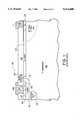
- FIG. 1is a cross section of an N-channel LDD lateral DMOS transistor 100 showing the double-diffused N+ source region 102 and P-body region 103.
- the P-body and source regions 103 and 102are commonly connected by conductor 120, which connects the P-body region 108 via the P+ contact region 101.
- the drain of transistor 100is formed by the N- LDD or drift region 122 and the N+ contact region 107.
- Transistor 100is controlled by the voltage of gate 109, which is situated above the gate oxide 110 and enclosed by insulation layer 121.
- a deep P+ region 104can be formed to provide a good contact to the P- substrate 105.
- This deep P+ region 104does not significantly impact the breakdown voltage of transistor 100, nor increases the parasitic capacitance associated with the transistor 100.
- An optional N-well 106can also be formed to provide a "deep" drain region suitable for longer-drift high-voltage devices requiring a higher breakdown voltage. Transistor breakdown often occurs at the high electric field associated with the edge of the drift region 122 next to the N+ contact region 107 ("drain-edge”), if the drift region 122 is very lightly doped. Alternatively, breakdown is more likely to occur at the edge of the drift region 122 next to the gate 109 ("gate-edge”), if the drift region 122 is relatively more heavily doped.
- a higher dopant concentration in the drift region 122reduces the on-resistance of the transistor 100, thereby allowing a higher saturation current.
- a breakdown at the surface near the gate-edge of drift region 122may leave an amount of charge in the gate oxide 110, resulting in reliability problems and an unstable breakdown voltage.
- FIG. 2shows the electrical potential distribution when transistor 100 is in the "off" state. (In FIG. 2, the optional deep P+ region 104 and the optional N-well 106 are not shown). As shown in FIG. 2, high electric fields are indicated by the closely-spaced electrical equipotential lines "crowding" at the gate-edge of the drift region 122. The distribution of high electric fields at the gate edge lowers the breakdown voltage of transistor 100.
- FIG. 3illustrates one method in the prior art to relieve the crowding of electrical equipotential lines, and thereby increases the breakdown voltage of transistor 100.
- a conductor 111called a field plate, which is electrically connected either to the gate 109 or the source region 102, is situated above the gate-edge of the drift region 122.
- the presence of the field plate 111reduces the crowding of equipotentials at the gate-edge of the drift region 122 above the silicon surface, and hence lowers the electric field intensities at the gate-edge.
- the field plate 111can be formed using polysilicon or metal. (When the field plate is electrically connected to the gate 109, the field plate is also known as the "gate plate").
- RESURFreduced surface field
- FIG. 4shows a junction-isolated RESURF lateral DMOS transistor 200 having a field-shaping P+ buried layer 201.
- transistor 200is fabricated in an N- epitaxial layer 206 formed on top of the P- substrate 205.
- Transistor 200comprises the N+ source and drain regions 202 and 207, the P-body region 203, and gate 209, which is formed above a gate oxide layer 210 and enclosed in the insulator layer 221.
- the N+ source region 202 and the P-body region 203are commonly connected by the metallization 220.
- transistor 200is provided a field-shaping buried layer 201, which extends from the P+ isolation 204 and reaches horizontally underneath the gate region beyond the gate-edge of the drift region 222.
- the field-shaping P+ buried layer 201enhances the breakdown voltage further by "uncrowding" the equipotential lines in the N- epitaxial layer 206 next to the gate region underneath 209.
- a similar transistoris disclosed in U.S. Pat. No. 4,300,150, entitled “lateral Double-diffused MOS transistor Device," by S. Colak, filed Jun. 16, 1980 and issued Nov. 10, 1981.
- RESURF lateral DMOS transistor 200 of FIG. 4has its breakdown voltage enhanced, due to both the use of the RESURF technique and the field-shaping P+ buried layer 201, RESURF lateral DMOS transistor 200 is expensive from the packing density stand point because additional area is required by the P+ isolation region 204.
- the P+ isolation region 204must be appropriately shaped, as shown in FIG. 4, to short the emitter-to-base junction of the high-gain parasitic vertical NPN transistor formed by the N+ source region 202, the P-body region 203, and the epitaxial region 206.
- BV CEO snapbackcommon-emitter base-open breakdown voltage snap-back
- the P-body region 203 of RESURF lateral DMOS transistor 200 of FIG. 4forms a reversed-bias junction with the N- epitaxial layer 206.
- Such reversed-biased junctionincreases the likelihood of punchthrough (barrier lowering) breakdown degradation in RESURF lateral DMOS transistor 200.
- punchthroughcarrier lowering
- the ability to integrate other bipolar or high voltage devicesmay be restricted by design considerations of the RESURF lateral DMOS transistor.
- a self-isolated LDD lateral DMOS transistor having reduced peak electric field at the gate-edge of the drift regionis highly desirable. Such transistor would allow a higher dopant concentration in the drift region without reliability or breakdown voltage degradation. Further, such self-isolated LDD lateral DMOS transistor provides the breakdown voltage and reliability characteristics without incurring the area penalty of the P+ isolation in a RESURF type lateral DMOS transistor, and allows the designer further freedom to select and use thicker epitaxial layers for other purposes, such as for providing a vertical NPN transistor.
- a self-isolated LDD lateral DMOS transistorhaving reduced peak electric fields at the gate edge without the added area cost of a RESURF transistor.
- the self-isolated LDD lateral DMOS transistoris formed in a lightly-doped epitaxial layer having the same conductivity type as the conductivity types of the substrate, a double-diffused body region and a buried layer.
- the buried layerextends from a position substantially beneath the source region to a position substantially beneath the drift region.
- a conductive gate plate(which may be metal, doped polysilicon, or any other appropriate conductive material) is provided above the gate region of the self-isolated lateral DMOS transistor.
- a deep body diffusion regionis provided in the self-isolated DMOS transistor.
- a deep drain diffusion regionis provided in the self-isolated DMOS transistor.
- the gate, the buried P+ layer and the drift regions of the self-isolated LDD lateral DMOS transistorform a substantially annular structure surrounding the drain region.
- the buried layerin conjunction with the structure or structures mentioned above, provides field-shaping flexibility to increase the breakdown voltage by relieving electric field crowding.
- the drift and the buried P+ regionsform a substantially annular structure surrounding the drain region.
- only one portion of the drift regionis bordered by the channel region; another portion of the drift region abuts an "inactive edge" formed by a field oxide layer and the drift region.
- a P+ buried layer underneath the inactive edgeis provided to reduce the electric field intensity at the inactive edge.
- a diodeis formed by eliminating the active channel region of an LDD lateral DMOS transistor.
- the P+ buried layerreduces the electric fields at the drift/field oxide interface, and improves the cathode-to-anode reverse-recovery characteristics.
- a field oxide regionis formed over the drift region prior to formation of the gate.
- the gateis extended over the field oxide region so as to reduce the electric field intensity at the interface between the channel and the drift regions.
- FIG. 1shows a self-isolated LDD lateral DMOS transistor in the prior art.
- FIG. 2shows the electrical equipotential distribution for the self-isolated LDD lateral DMOS transistor of FIG. 1.
- FIG. 3shows the electrical equipotential distribution for a prior art self-isolated LDD lateral DMOS transistor having a gate plate.
- FIG. 4shows a prior art RESURF type lateral DMOS transistor having a buried P+ layer.
- FIG. 5shows a self-isolated LDD lateral DMOS transistor 500 with a field-shaping P+ buried layer 501, in accordance with an embodiment of the present invention.
- FIG. 6shows the electrical equipotential distribution for the self-isolated LDD lateral DMOS transistor 500 of FIG. 5.
- FIG. 7shows a self-isolated LDD lateral DMOS transistor 600 with an N-well 606, in accordance with another embodiment of the present invention.
- FIG. 8compares the electric field distributions of the LDD lateral DMOS transistor of FIG. 1, the LDD lateral DMOS transistor of FIG. 2 (i.e. with a gate plate) and the LDD lateral DMOS transistor 500 of FIG. 5, provided in accordance with the present invention.
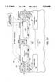
- FIG. 9shows high-voltage LDD lateral DMOS transistor 900 in accordance with the present invention integrated with low-voltage CMOS transistors 903 and 904 each using P+ and N+ buried layers to suppress the CMOS latch up phenomenon.
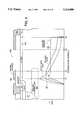
- FIG. 10ais a cross section of a self-isolated LDD lateral DMOS transistor 1000 having a partial inactive edge 1051 and a P+ buried layer 501 underneath the partial inactive edge, in accordance with the present invention.
- FIG. 10bis a top view of the self-isolated lateral DMOS transistor 1000 shown in FIG. 10a.
- FIG. 11is a cross section of a self-isolated LDD diode 1100 having a P+ buried layer 501 underneath a drift region 522, the drift region 522 being formed beneath a field oxide layer 1050, in accordance with the present invention.
- FIG. 12is a cross section of a self-isolated LDD lateral DMOS transistor 1200 having a P+ buried layer 501 partially overlapped by the N- drift region 1222; the N- drift region 1222 being formed beneath a field oxide layer 1250, in accordance with the present invention.
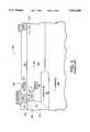
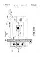
- FIG. 5shows a cross section of an LDD lateral DMOS transistor 500 provided in accordance with one embodiment of the present invention.
- LDD lateral DMOS transistor 500is a substantially annular structure in which the gate 509, the drift region 522 and the P+ buried layer 501 (see below) surround the drain region on all sides.
- LDD lateral DMOS transistor 500is formed in a lightly-doped P- epitaxial layer 512 on top of a P- substrate 505.
- the epitaxial layer 512has a dopant (e.g. boron) concentration typically 1.0 ⁇ 10 14 /cm 3 to 5.0 ⁇ 10 14 /cm 3 , although the dopant concentration can be as high as 8.0 ⁇ 10 15 /cm 3 .
- the depth of the epitaxial layeris chosen according to the intended operational conditions of all devices in the integrated circuit.
- the resistivity of the P- (e.g. boron-doped) substrate 505is chosen with consideration of the intended maximum operational voltage of all devices integrated with transistor 500 in the integrated circuit.
- a 30-50 ohms-cm resistivitycan be used for up to 500 volts. However, for higher voltage operations (e.g. 1000 volts or higher), a higher resistivity, even up to several hundred ohms-cm, can be used.
- the P- epitaxial layer 512can be deposited by high temperature chemical vapor deposition, or any other suitable technique known in the art.
- the P+ buried layer 501is formed by conventional technique, such as ion implantation, near the surface of the P- substrate 505.
- the P+ buried layer 501back diffuses towards the surface of the P- epitaxial layer 512.
- an initial dopant concentrationis provided such that the final dopant concentration of the P+ buried layer 501 is in the order of 10 16 /cm 3 .
- a 5.0 ⁇ 10 14 /cm 2 implant dose of boron at 60 KeVprovides the desirable final dopant concentration in the P+ buried layer 501. Since the back diffusion can be as much as 8 microns, this thickness limits the minimum depth the P- epitaxial layer 512 can be.
- FIG. 5shows a deep P+ region 504 which, though not necessary, provides a better contact between the P-body region 502 and the P- substrate 505.
- a boron dose in excess of 10 15 /cm 2 at 60 KeVcan be used.
- the P+ region 504can be formed using a P+ predeposition from a gaseous or solid boron source.
- the P-body region 503determines the threshold voltage of the LDD lateral DMOS transistor 500.
- the implant dose (at 60 KeV) used to form the P-body region 503ranges from 1.0 ⁇ 10 13 /cm 2 to 9.0 ⁇ 10 13 /cm 2 , dependent upon the desired threshold voltage, with a typical dose of 5.0 ⁇ 10 13 /cm 2 .
- the threshold voltage for common N+/P-body junction depthsvary from 0.7 volts to 3.0 volts, depending on the net profile as determined by the interaction in the junction between N+ 502 and P-body region 503.
- the P-body region 503down-diffuses as deep as 4 microns into the substrate.
- the RESURF type LDD lateral DMOS transistorsuch as transistor 200 shown in FIG.
- a reversed-bias junctionis formed between the N+ drain 507 and the P- epitaxial layer 512, which is too far from the P-body region 503 to contribute to punchthrough breakdown degradation of the transistor 500.
- the N+ source region 502 and the N+ drain region 507are formed using conventional techniques with an implant dose of 5.0 ⁇ 10 15 /cm 2 or higher. In this embodiment, 50%--50% mixture of phosphorus and arsenic is used, although either dopant can be used without the other. Because of the benefits of the present invention (explained below), the drift region can be formed with a total implant dose (e.g. phosphorous) up to 4.0 ⁇ 10 12 /cm 2 , which is approximately four times the dopant implant dose of drift regions attainable in the prior art. The on-resistance of this transistor 500 is therefore much reduced from that of LDD lateral DMOS transistors in the prior art.
- N-well 506can also be provided.
- N-well 506can be 3-12 microns deep, with a dopant concentration (e.g. phosphorous) between 1.0 ⁇ 10 15 /cm 3 to 2.0 ⁇ 10 16 /cm 3 .
- an implant dosee.g. phosphorous
- 3.0-8.0 ⁇ 10 12 /cm 2 at 60-100 KeVcan be used to provide a typical surface concentration of substantially 8.0 ⁇ 10 15 /cm 3 .
- the optional N-well 506provides additional field-shaping flexibility (explained below).
- An optional P+ region 513(e.g. boron-doped) provides a source-P-body shunt and provides better contact to the P-body region 503. If the P+ region 513 is not provided, the P-body region 503 contacts the source/body contact 520 directly, or in combination with deep P+ region 504.
- the gate oxide 510 and the gate 509 of transistor 500are formed using conventional method.
- an optional gate plate 511e.g. aluminum
- the conducting material 508 at the drain contact region 507can also be made to extend over the insulation layer 521 beyond the drain-edge of the drift region 522 forming a field plate.
- the electrical equipotential distribution of transistor 500is shown in FIG. 6.
- the presence of the P+ buried layer 501pushes the electrical equipotential lines beneath the silicon surface laterally further and more evenly in the direction of the drain contact region 507.
- the crowding of electrical equipotentials indicated by arrow A in FIG. 3is relieved by the presence of P+ buried layer 501.
- the breakdown voltage of LDD DMOS transistor 500is enhanced by both the reduction of the electric fields at the gate-edge of the drift region 522, and by the shifting of the electric fields into the bulk silicon away from the surface charges.
- the dopant concentration in the drift region 522can be increased up to four times over the prior art, correspondingly reducing the on-resistance of the transistor 500, thereby increasing LDD lateral DMOS transistor 500's ability to sustain a higher current. Furthermore, because the breakdown remains in the bulk, the avalanche breakdown voltage remains stable, and the charging of the overlying oxide 521 is minimized.
- FIG. 7shows in another embodiment of the present invention the electrical equipotential distribution of an LDD lateral DMOS transistor 600 having an N-well 606.
- N-well 606also pushes the electrical equipotentials of transistor 600 further into the bulk silicon and away from the surface charges.
- controlling the depth of N-well 606provides further field-shaping flexibility for tailoring transistor 600 to the desired breakdown characteristics.
- N-wells, such as N-well 606,are commonly used for operating voltages above 200 volts, but are less commonly used if the operating voltage is less than 200 volts. This is because desirable breakdown characteristics are more easily achieved at less than 200 volts.
- An N-wellalso reduces the on-resistance of the high voltage transistors.
- FIG. 8compares the electric field intensities along the silicon surface of (a) an LDD lateral DMOS transistor in the prior art similar to that shown in FIG. 1; (b) an LDD lateral DMOS transistor similar to the transistor in (a), but having a gate plate such as the gate plate 802 shown; and (c) an LDD lateral DMOS transistor having a P+ buried layer, such as P+ buried layer 801 shown in accordance with the present invention.
- FIG. 8compares the electric field intensities along the silicon surface of (a) an LDD lateral DMOS transistor in the prior art similar to that shown in FIG. 1; (b) an LDD lateral DMOS transistor similar to the transistor in (a), but having a gate plate such as the gate plate 802 shown; and (c) an LDD lateral DMOS transistor having a P+ buried layer, such as P+ buried layer 801 shown in accordance with the present invention.
- P+ buried layer 801shown in accordance with the present invention.
- the transistor in (a)is represented by the structure 800, minus the gate plate 802 and the P+ buried layer 801; the transistor in (b) is represented by the structure 800, minus the P+ buried layer 801; and the transistor in (c) is represented by the structure 800, with both the gate plate 802 and the P+ buried layer 801. All three transistors in (a) and (b) and (c) have the drain plate 804.
- the drain plate 804modifies the field distribution at the drain-edge of the drift region 805, in the manner discussed above.
- the electric field intensities along the surface of the siliconis plotted against the distance in the x-direction.
- the curves labelled 820, 821 and 822represent respectively the electric field intensity profiles of the transistors in (a), (b) and (c) described above. It is readily seen that in all three curves 820, 821 and 822, the electric field intensity peaks at the gate-edge (point x 1 ) of the drift region 805, and approaches zero at the drain-edge (point x 4 ) of the drift region 805. As expected, the highest electric field intensity at point x 1 corresponds to the transistor in (a).
- the electric field intensity (curve 820)rapidly falls off as the distance from the gate-edge of the drift region increases.
- the electric fieldin this instance, decreases at a rate which is moderated by the presence of the drain plate 804 between points x 3 and x 4 .
- the electric field intensity (curve 821)is more or less level for the region underneath the gate plate 802, and then decreases at a substantially constant rate similar to the rate of decrease shown in curve 820, as one moves beyond the extent of the gate plate 802 at point x 2 towards point x 4 .
- curves 820 and 821illustrate, both the gate and the drain plates 802 and 804 have a levelling effect on the electric field intensity along the silicon surface under these plates.
- transistor (c) having the P+ buried layer 801has a substantially uniform electric field intensity profile along the entire length (x 1 to x 4 ) of the drift region 805.
- the P+ buried layerreduces the injected minority carrier lifetime, thereby improving the reverse-recovery characteristics in the diode formed by the drain 507, the P- epitaxial layer 512 and the P- substrate 505.
- P+ buried layerscan also be formed beneath the low-voltage NMOS transistors used to implement the circuits, such as logic circuits, integrated on the same semiconductor substrate. The buried layers under such low-voltage NMOS transistors reduce the integrated circuit's susceptibility to the CMOS latch-up condition.
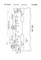
- FIG. 9shows an LDD lateral DMOS transistor 901 formed in an annular fashion, integrated on the same substrate as two low-voltage CMOS transistors 903 and 904.
- the P+ buried layers 905 and 906serve not only as field-shaping structures for transistor 901, but also as a latch-up suppressing structure for NMOS transistor 904.
- the drift, drain, P-body, the various P+ buried regions, and other structures of LDD lateral DMOS transistor 901are annular structures.
- the conductor 910which connects both the P-body regions and source regions of LDD lateral DMOS transistor 901 is shown in FIG. 9 as annular.
- FIG. 10ashows an LDD lateral DMOS transistor 1000, which is similar to transistor 500 of FIG. 5, except that in transistor 1000, only a portion of the drift region 522 borders an active channel region under the gate 1009. That is, unlike gate 509 of transistor 500, gate 1009 of transistor 1000 is not an annular structure surrounding the drain region 507.
- the same reference numerals in FIGS. 5 and FIGS. 10adenote structures which are functionally and structurally alike.
- the source/bulk contact 1020, the P+ region 1013, and the P-body region 1003 of transistor 1000are similar in function to corresponding source/bulk contact 502, the P+ region 513 and the P-body region 503 of transistor 500, and can be formed in substantially the same manner as described above for transistor 500.
- a field oxide region 1050is formed by a LOCOS process known in the art.
- This oxide region 1050which is typically between 5000 ⁇ to 2 microns thick, is formed prior to formation of gate 1009 and shown in FIG. 10a to abut the drift region 522 on the side of the drift region 522 away from the channel region.
- the interface 1051 between the drift region 522 and the field oxide region 1050is known as the "inactive edge”
- the interface 1052 between the drift region 522 and the channel regionis known as the "active edge.”
- an adverse high electric fieldmay develop at the inactive edge 1051.
- This adverse high electric fieldmay be further increased by the presence of P-type field dopant, or by stress-induced crystalline defects present at the interface between oxide region 1050 and the drift region 522.
- One source of such crystalline defectsis the LOCOS field oxidation step mentioned above. Therefore, in accordance with the present invention there is provided underneath the inactive edge a portion of the P+ buried layer 501. This portion of the P+ buried layer 501 pushes the electrical equipotential lines away from the inactive edge 1051 and into the bulk silicon in substantially the same manner as provided by the P+ buried layer 501 underneath the active edge 1052 described above.
- FIG. 10bThe top view of one possible layout of the transistor 1000 is shown in FIG. 10b.
- the inactive edge 1051 and the active edge 1052are shown to be on opposite sides of the drain region 507.
- the extent of the P+ buried layer 501, the drift region 522, and the optional gate plate 511are indicated respectively by bidirectional arrows 1061, 1062 and 1063.
- Field oxide 1050lies outside the solid rectangle, 1057.
- Gate 509, source/bulk contact 520, and the source region 502are also indicated.
- a diode structurecan result from eliminating the active gate from an LDD lateral DMOS transistor, such as transistor 1000 of FIG. 10a.
- Such a diodeis shown in FIG. 11, giving the same reference numerals to corresponding structures in FIGS. 10a and 11.
- a diodeis formed by the P substrate 505 (anode), the P-epitaxial layer 512 and the drain region 507 (cathode).
- the P substrate layeris connected in common with the source contact 1020, and the P+ region 1013.
- the P+ buried layer 501pushes the electrical equipotential lines away from the inactive edge 1051 and into the bulk silicon to relieve high electric field that can developed at the inactive edge.
- the P+ buried layer 501reduces the injected minority carrier lifetime, and thereby improves the cathode-to-anode reverse-recovery characteristics of the diode.
- FIG. 12is another embodiment of the present invention in an LDD lateral DMOS transistor 1200, in which a field oxide region 1250 is formed over the drift region 1222.
- transistor 1200is a substantially annular structure having gate 1209, drift region 1222, and the P+ buried layer 501 surround the drain region 507.
- like structures of the transistors 500 and 1200are given the same reference numerals.
- the like structures of transistors 500 and 1200can be formed in substantially the same manner as described above for transistor 500.
- the drift region 1222can be formed in the same manner as the drift region 522 of transistor 500.
- the field oxide layer 1250is not found in transistor 500 of FIG. 5.
- This field oxide region 1250which may be formed by the LOCOS process mentioned above, is distinguished from other available oxide layers in that it can be any thick oxide formed prior to the formation of gate 1209, thereby allowing an overlap of the gate 1209 to be formed over part of the field oxide 1250, as shown in FIG. 12.
- This overlap by the gate 509 over the field oxide 1250forms an effective gate plate to prevent high electric field at the interface 1251 between the channel region 1253 and the drift region 1222, thereby further enhancing the breakdown voltage of transistor 1200.
Landscapes
- Insulated Gate Type Field-Effect Transistor (AREA)
- Metal-Oxide And Bipolar Metal-Oxide Semiconductor Integrated Circuits (AREA)
Abstract
Description
Claims (18)
Priority Applications (1)
| Application Number | Priority Date | Filing Date | Title |
|---|---|---|---|
| US08/318,027US5514608A (en) | 1991-05-06 | 1994-10-04 | Method of making lightly-doped drain DMOS with improved breakdown characteristics |
Applications Claiming Priority (2)
| Application Number | Priority Date | Filing Date | Title |
|---|---|---|---|
| US07/697,356US5386136A (en) | 1991-05-06 | 1991-05-06 | Lightly-doped drain MOSFET with improved breakdown characteristics |
| US08/318,027US5514608A (en) | 1991-05-06 | 1994-10-04 | Method of making lightly-doped drain DMOS with improved breakdown characteristics |
Related Parent Applications (1)
| Application Number | Title | Priority Date | Filing Date |
|---|---|---|---|
| US07/697,356DivisionUS5386136A (en) | 1991-05-06 | 1991-05-06 | Lightly-doped drain MOSFET with improved breakdown characteristics |
Publications (1)
| Publication Number | Publication Date |
|---|---|
| US5514608Atrue US5514608A (en) | 1996-05-07 |
Family
ID=24800813
Family Applications (2)
| Application Number | Title | Priority Date | Filing Date |
|---|---|---|---|
| US07/697,356Expired - LifetimeUS5386136A (en) | 1991-05-06 | 1991-05-06 | Lightly-doped drain MOSFET with improved breakdown characteristics |
| US08/318,027Expired - LifetimeUS5514608A (en) | 1991-05-06 | 1994-10-04 | Method of making lightly-doped drain DMOS with improved breakdown characteristics |
Family Applications Before (1)
| Application Number | Title | Priority Date | Filing Date |
|---|---|---|---|
| US07/697,356Expired - LifetimeUS5386136A (en) | 1991-05-06 | 1991-05-06 | Lightly-doped drain MOSFET with improved breakdown characteristics |
Country Status (5)
| Country | Link |
|---|---|
| US (2) | US5386136A (en) |
| EP (1) | EP0514060B1 (en) |
| JP (3) | JP3425967B2 (en) |
| DE (1) | DE69224446T2 (en) |
| SG (1) | SG45292A1 (en) |
Cited By (68)
| Publication number | Priority date | Publication date | Assignee | Title |
|---|---|---|---|---|
| US5602046A (en)* | 1996-04-12 | 1997-02-11 | National Semiconductor Corporation | Integrated zener diode protection structures and fabrication methods for DMOS power devices |
| US5747850A (en)* | 1994-04-08 | 1998-05-05 | Texas Instruments Incorporated | Extended drain resurf lateral DMOS devices |
| US5852559A (en)* | 1996-09-24 | 1998-12-22 | Allen Bradley Company, Llc | Power application circuits utilizing bidirectional insulated gate bipolar transistor |
| US5891757A (en)* | 1995-11-30 | 1999-04-06 | Nec Corporation | Method for forming a field-effect transistor having difference in capacitance between source and drain with respect to shield layer |
| WO1999026296A3 (en)* | 1997-11-13 | 1999-07-29 | Abb Research Ltd | A SEMICONDUCTOR DEVICE OF SiC AND A TRANSISTOR OF SiC HAVING AN INSULATED GATE |
| US5977569A (en)* | 1996-09-24 | 1999-11-02 | Allen-Bradley Company, Llc | Bidirectional lateral insulated gate bipolar transistor having increased voltage blocking capability |
| US5981344A (en)* | 1992-07-24 | 1999-11-09 | Siliconix Incorporated | Trench field effect transistor with reduced punch-through susceptibility and low RDSon |
| WO1999057761A1 (en)* | 1998-05-04 | 1999-11-11 | Xemod, Inc. | Method for fabricating a lateral rf mos device with a non-diffusion source-backside connection |
| US6063678A (en)* | 1998-05-04 | 2000-05-16 | Xemod, Inc. | Fabrication of lateral RF MOS devices with enhanced RF properties |
| US6096610A (en)* | 1996-03-29 | 2000-08-01 | Intel Corporation | Transistor suitable for high voltage circuit |
| US6242787B1 (en) | 1995-11-15 | 2001-06-05 | Denso Corporation | Semiconductor device and manufacturing method thereof |
| WO2001047024A1 (en)* | 1999-12-21 | 2001-06-28 | Koninklijke Philips Electronics N.V. | Silicon carbide n-channel power lmosfet |
| US6365932B1 (en) | 1999-08-20 | 2002-04-02 | Denso Corporation | Power MOS transistor |
| US6369426B2 (en) | 2000-04-27 | 2002-04-09 | Infineon Technologies North America Corp. | Transistor with integrated photodetector for conductivity modulation |
| US6395610B1 (en) | 1999-06-24 | 2002-05-28 | Lucent Technologies Inc. | Method of making bipolar transistor semiconductor device including graded, grown, high quality oxide layer |
| US20020117714A1 (en)* | 2001-02-28 | 2002-08-29 | Linear Technology Corporation | High voltage MOS transistor |
| US6448611B1 (en)* | 1999-06-07 | 2002-09-10 | Hynix Semiconductor, Inc. | High power semiconductor device and fabrication method thereof |
| US20030006467A1 (en)* | 2001-06-15 | 2003-01-09 | Sandra Mattei | Lateral MOS power transistor |
| US6509230B1 (en) | 1999-06-24 | 2003-01-21 | Lucent Technologies Inc. | Non-volatile memory semiconductor device including a graded, grown, high quality oxide layer and associated methods |
| US6521496B1 (en) | 1999-06-24 | 2003-02-18 | Lucent Technologies Inc. | Non-volatile memory semiconductor device including a graded, grown, high quality control gate oxide layer and associated methods |
| US20030047792A1 (en)* | 2001-09-07 | 2003-03-13 | Power Integrations, Inc. | High-voltage lateral transistor with a multi-layered extended drain structure |
| US20030047793A1 (en)* | 2001-09-07 | 2003-03-13 | Power Integrations, Inc. | High-voltage vertical transistor with a multi-layered extended drain structure |
| US20030060001A1 (en)* | 2001-09-07 | 2003-03-27 | Power Integrations, Inc. | Method of fabricating a high-voltage transistor with a multi-layered extended drain structure |
| US6551946B1 (en) | 1999-06-24 | 2003-04-22 | Agere Systems Inc. | Two-step oxidation process for oxidizing a silicon substrate wherein the first step is carried out at a temperature below the viscoelastic temperature of silicon dioxide and the second step is carried out at a temperature above the viscoelastic temperature |
| US20030109112A1 (en)* | 2001-12-07 | 2003-06-12 | Texas Instruments Incorporated | Method of manufacturing and structure of semiconductor device with field oxide structure |
| US20030178646A1 (en)* | 2001-01-24 | 2003-09-25 | Power Integrations, Inc. | High-voltage transistor with buried conduction layer |
| US6638824B2 (en) | 1998-12-28 | 2003-10-28 | Fairchild Semiconductor Corporation | Metal gate double diffusion MOSFET with improved switching speed and reduced gate tunnel leakage |
| US20030235957A1 (en)* | 2002-06-25 | 2003-12-25 | Samir Chaudhry | Method and structure for graded gate oxides on vertical and non-planar surfaces |
| US6670242B1 (en) | 1999-06-24 | 2003-12-30 | Agere Systems Inc. | Method for making an integrated circuit device including a graded, grown, high quality gate oxide layer and a nitride layer |
| KR100425435B1 (en)* | 2002-02-08 | 2004-03-30 | 페어차일드코리아반도체 주식회사 | Lateral DMOS transistor having RESURF structure and method for fabricating the same |
| US20040063291A1 (en)* | 2002-09-29 | 2004-04-01 | Williams Richard K. | Modular bipolar-CMOS-DMOS analog integrated circuit & power transistor technology |
| US20040159891A1 (en)* | 2003-02-18 | 2004-08-19 | Kabushiki Kaisha Toshiba | Semiconductor device |
| US20040232510A1 (en)* | 2001-06-28 | 2004-11-25 | John Petruzzello | HV-SOI LDMOS device with integrated diode to improve reliability and avalanche ruggedness |
| US6831331B2 (en) | 1995-11-15 | 2004-12-14 | Denso Corporation | Power MOS transistor for absorbing surge current |
| US20050006701A1 (en)* | 2003-07-07 | 2005-01-13 | Tzu-Chiang Sung | High voltage metal-oxide semiconductor device |
| US20050133858A1 (en)* | 2001-09-07 | 2005-06-23 | Power Integrations, Inc. | High-voltage vertical transistor with a multi-gradient drain doping profile |
| US20060011981A1 (en)* | 2004-07-15 | 2006-01-19 | Samsung Electronis Co., Ltd. | High frequency MOS transistor, method of forming the same, and method of manufacturing a semiconductor device including the same |
| KR100532367B1 (en)* | 1998-09-16 | 2006-01-27 | 페어차일드코리아반도체 주식회사 | Lateral diffusion MOS transistor having the protection diode and the fabrication method thereof |
| US7078296B2 (en) | 2002-01-16 | 2006-07-18 | Fairchild Semiconductor Corporation | Self-aligned trench MOSFETs and methods for making the same |
| US20070007591A1 (en)* | 2003-08-27 | 2007-01-11 | Theeuwen Stephan Jo Cecile H | Electric device comprising an ldmos transistor |
| CN100361315C (en)* | 2003-09-30 | 2008-01-09 | 因芬尼昂技术股份公司 | Vertical DMOS transistor device, integrated circuit and manufacturing method thereof |
| US20080087963A1 (en)* | 2006-09-29 | 2008-04-17 | Calafut Daniel S | TAPERED VOLTAGE POLYSILICON DIODE ELECTROSTATIC DISCHARGE CIRCUIT FOR POWER MOSFETS AND ICs |
| JP2008140817A (en)* | 2006-11-30 | 2008-06-19 | Toshiba Corp | Semiconductor device |
| US20080167196A1 (en)* | 2000-02-06 | 2008-07-10 | Stefan Dickopf | Surface for the immobilization of ligands |
| US20080197406A1 (en)* | 2007-02-16 | 2008-08-21 | Power Integrations, Inc. | Sensing FET integrated with a high-voltage vertical transistor |
| US20080197397A1 (en)* | 2007-02-16 | 2008-08-21 | Power Integrations, Inc. | Checkerboarded high-voltage vertical transistor layout |
| US20080197417A1 (en)* | 2007-02-16 | 2008-08-21 | Power Integrations, Inc. | Segmented pillar layout for a high-voltage vertical transistor |
| US20080197418A1 (en)* | 2007-02-16 | 2008-08-21 | Power Integrations, Inc. | Gate pullback at ends of high-voltage vertical transistor structure |
| US7468536B2 (en) | 2007-02-16 | 2008-12-23 | Power Integrations, Inc. | Gate metal routing for transistor with checkerboarded layout |
| US20090194785A1 (en)* | 2008-01-11 | 2009-08-06 | Fuji Electric Device Technology Co., Ltd. | Semiconductor device and manufacturing method thereof |
| US20100032758A1 (en)* | 2008-08-06 | 2010-02-11 | United Microelectronics Corp. | Ldmos device for esd protection circuit |
| US20100065909A1 (en)* | 2008-09-17 | 2010-03-18 | Sharp Kabushiki Kaisha | Semiconductor device and method for making the same |
| US20100102379A1 (en)* | 2008-10-29 | 2010-04-29 | United Microelectronics Corp. | Lateral diffused metal oxide semiconductor device |
| US20100173463A1 (en)* | 2009-01-06 | 2010-07-08 | Nam-Joo Kim | Lateral double diffused metal oxide semiconductor |
| US7786533B2 (en) | 2001-09-07 | 2010-08-31 | Power Integrations, Inc. | High-voltage vertical transistor with edge termination structure |
| US20120175679A1 (en)* | 2011-01-10 | 2012-07-12 | Fabio Alessio Marino | Single structure cascode device |
| US20130071994A1 (en)* | 2011-09-20 | 2013-03-21 | Alpha And Omega Semiconductor Incorporated | Method of integrating high voltage devices |
| US20130069157A1 (en)* | 2011-09-20 | 2013-03-21 | Alpha And Omega Semiconductor Incorporated | Semiconductor chip integrating high and low voltage devices |
| US20130187226A1 (en)* | 2012-01-20 | 2013-07-25 | SK Hynix Inc. | Lateral double diffused mos transistors and methods of fabricating the same |
| US8673712B2 (en)* | 2012-07-20 | 2014-03-18 | Taiwan Semiconductor Manufacturing Company, Ltd. | Power transistor with high voltage counter implant |
| CN104576375A (en)* | 2013-10-12 | 2015-04-29 | 中芯国际集成电路制造(上海)有限公司 | LDMOS (laterally diffused metal oxide semiconductor) and manufacture method thereof |
| US9257504B2 (en) | 2002-09-29 | 2016-02-09 | Advanced Analogic Technologies Incorporated | Isolation structures for semiconductor devices |
| US9425788B1 (en) | 2015-03-18 | 2016-08-23 | Infineon Technologies Austria Ag | Current sensors and methods of improving accuracy thereof |
| US9543396B2 (en) | 2013-12-13 | 2017-01-10 | Power Integrations, Inc. | Vertical transistor device structure with cylindrically-shaped regions |
| US10090309B1 (en) | 2017-04-27 | 2018-10-02 | Ememory Technology Inc. | Nonvolatile memory cell capable of improving program performance |
| US10325988B2 (en) | 2013-12-13 | 2019-06-18 | Power Integrations, Inc. | Vertical transistor device structure with cylindrically-shaped field plates |
| US20190245034A1 (en)* | 2012-07-31 | 2019-08-08 | Silanna Asia Pte Ltd | Power device integration on a common substrate |
| US10937872B1 (en)* | 2019-08-07 | 2021-03-02 | Vanguard International Semiconductor Corporation | Semiconductor structures |
Families Citing this family (108)
| Publication number | Priority date | Publication date | Assignee | Title |
|---|---|---|---|---|
| US5374569A (en)* | 1992-09-21 | 1994-12-20 | Siliconix Incorporated | Method for forming a BiCDMOS |
| US5446300A (en)* | 1992-11-04 | 1995-08-29 | North American Philips Corporation | Semiconductor device configuration with multiple HV-LDMOS transistors and a floating well circuit |
| JP3221766B2 (en)* | 1993-04-23 | 2001-10-22 | 三菱電機株式会社 | Method for manufacturing field effect transistor |
| US5378912A (en)* | 1993-11-10 | 1995-01-03 | Philips Electronics North America Corporation | Lateral semiconductor-on-insulator (SOI) semiconductor device having a lateral drift region |
| JPH07183407A (en)* | 1993-12-22 | 1995-07-21 | Nec Corp | Nonvolatile semiconductor memory device |
| DE19517975B4 (en)* | 1994-07-12 | 2007-02-08 | International Rectifier Corp., El Segundo | CMOS circuit chips with polysilicon field ring structure |
| US5598021A (en)* | 1995-01-18 | 1997-01-28 | Lsi Logic Corporation | MOS structure with hot carrier reduction |
| KR970004074A (en)* | 1995-06-05 | 1997-01-29 | 빈센트 비. 인그라시아 | Insulated gate field effect transistor and its manufacturing method |
| JPH10506503A (en)* | 1995-07-19 | 1998-06-23 | フィリップス エレクトロニクス ネムローゼ フェンノートシャップ | HV-LDMOST type semiconductor device |
| US5817551A (en)* | 1995-08-25 | 1998-10-06 | Matsushita Electric Industrial Co., Ltd. | Semiconductor device and method of manufacturing the same |
| US5569937A (en)* | 1995-08-28 | 1996-10-29 | Motorola | High breakdown voltage silicon carbide transistor |
| US5753958A (en)* | 1995-10-16 | 1998-05-19 | Sun Microsystems, Inc. | Back-biasing in asymmetric MOS devices |
| US6207994B1 (en) | 1996-11-05 | 2001-03-27 | Power Integrations, Inc. | High-voltage transistor with multi-layer conduction region |
| US6168983B1 (en)* | 1996-11-05 | 2001-01-02 | Power Integrations, Inc. | Method of making a high-voltage transistor with multiple lateral conduction layers |
| US6800903B2 (en) | 1996-11-05 | 2004-10-05 | Power Integrations, Inc. | High-voltage transistor with multi-layer conduction region |
| US5825065A (en)* | 1997-01-14 | 1998-10-20 | Texas Instruments Incorporated | Low voltage DMOS transistor |
| US5939753A (en)* | 1997-04-02 | 1999-08-17 | Motorola, Inc. | Monolithic RF mixed signal IC with power amplification |
| KR100244282B1 (en) | 1997-08-25 | 2000-02-01 | 김영환 | Structure and manufacturing method of high voltage transistor |
| JP3175923B2 (en)* | 1997-11-05 | 2001-06-11 | 松下電子工業株式会社 | Semiconductor device |
| JP3270405B2 (en)* | 1998-01-26 | 2002-04-02 | セイコーインスツルメンツ株式会社 | Semiconductor device |
| US6020611A (en)* | 1998-06-10 | 2000-02-01 | Motorola, Inc. | Semiconductor component and method of manufacture |
| US6534829B2 (en)* | 1998-06-25 | 2003-03-18 | Matsushita Electric Industrial Co., Ltd. | Semiconductor device and method for fabricating the same |
| WO2000035020A1 (en)* | 1998-12-07 | 2000-06-15 | Infineon Technologies Ag | Lateral high-voltage semiconductor component with reduced specific closing resistor |
| JP2003509867A (en)* | 1999-09-16 | 2003-03-11 | コーニンクレッカ フィリップス エレクトロニクス エヌ ヴィ | Semiconductor device |
| DE10028008A1 (en)* | 2000-06-06 | 2001-12-13 | Bosch Gmbh Robert | Protection against electrostatic discharge for integrated circuit in semiconductor substrate |
| US6509220B2 (en) | 2000-11-27 | 2003-01-21 | Power Integrations, Inc. | Method of fabricating a high-voltage transistor |
| US6768171B2 (en) | 2000-11-27 | 2004-07-27 | Power Integrations, Inc. | High-voltage transistor with JFET conduction channels |
| EP1220323A3 (en)* | 2000-12-31 | 2007-08-15 | Texas Instruments Incorporated | LDMOS with improved safe operating area |
| JP2002353441A (en)* | 2001-05-22 | 2002-12-06 | Denso Corp | Power MOS transistor |
| KR100409093B1 (en)* | 2001-07-12 | 2003-12-11 | 주식회사 엘리아테크 | A high voltage device and method of wiring metal on it |
| JP3546037B2 (en)* | 2001-12-03 | 2004-07-21 | 松下電器産業株式会社 | Method for manufacturing semiconductor device |
| JP4524989B2 (en)* | 2001-12-18 | 2010-08-18 | 富士電機システムズ株式会社 | Semiconductor device |
| US6686627B2 (en)* | 2001-12-26 | 2004-02-03 | Sirenza Microdevices, Inc. | Multiple conductive plug structure for lateral RF MOS devices |
| US6617643B1 (en) | 2002-06-28 | 2003-09-09 | Mcnc | Low power tunneling metal-oxide-semiconductor (MOS) device |
| US7834421B2 (en)* | 2002-08-14 | 2010-11-16 | Advanced Analogic Technologies, Inc. | Isolated diode |
| US20080197408A1 (en)* | 2002-08-14 | 2008-08-21 | Advanced Analogic Technologies, Inc. | Isolated quasi-vertical DMOS transistor |
| US7956391B2 (en) | 2002-08-14 | 2011-06-07 | Advanced Analogic Technologies, Inc. | Isolated junction field-effect transistor |
| US8089129B2 (en)* | 2002-08-14 | 2012-01-03 | Advanced Analogic Technologies, Inc. | Isolated CMOS transistors |
| US8513087B2 (en)* | 2002-08-14 | 2013-08-20 | Advanced Analogic Technologies, Incorporated | Processes for forming isolation structures for integrated circuit devices |
| US7902630B2 (en)* | 2002-08-14 | 2011-03-08 | Advanced Analogic Technologies, Inc. | Isolated bipolar transistor |
| US7939420B2 (en)* | 2002-08-14 | 2011-05-10 | Advanced Analogic Technologies, Inc. | Processes for forming isolation structures for integrated circuit devices |
| US7667268B2 (en)* | 2002-08-14 | 2010-02-23 | Advanced Analogic Technologies, Inc. | Isolated transistor |
| US7173308B2 (en)* | 2002-10-25 | 2007-02-06 | Shindengen Electric Manufacturing Co., Ltd. | Lateral short-channel DMOS, method for manufacturing same and semiconductor device |
| DE10311699B4 (en)* | 2003-03-17 | 2007-07-26 | Infineon Technologies Ag | LOMOS high frequency transistor and method of making same |
| KR100948139B1 (en)* | 2003-04-09 | 2010-03-18 | 페어차일드코리아반도체 주식회사 | Horizontal double-diffusion MOS transistor with multi-current travel path for high breakdown voltage and low on-resistance |
| US6865093B2 (en)* | 2003-05-27 | 2005-03-08 | Power Integrations, Inc. | Electronic circuit control element with tap element |
| US7049669B2 (en)* | 2003-09-15 | 2006-05-23 | Infineon Technologies Ag | LDMOS transistor |
| JP2005116876A (en) | 2003-10-09 | 2005-04-28 | Toshiba Corp | Semiconductor device |
| US7304354B2 (en)* | 2004-02-17 | 2007-12-04 | Silicon Space Technology Corp. | Buried guard ring and radiation hardened isolation structures and fabrication methods |
| JP4618629B2 (en)* | 2004-04-21 | 2011-01-26 | 三菱電機株式会社 | Dielectric isolation type semiconductor device |
| US7002398B2 (en)* | 2004-07-08 | 2006-02-21 | Power Integrations, Inc. | Method and apparatus for controlling a circuit with a high voltage sense device |
| DE102005049247B4 (en) | 2004-11-05 | 2018-06-07 | Infineon Technologies Ag | High frequency switching transistor and high frequency circuit |
| KR100690173B1 (en)* | 2005-03-08 | 2007-03-08 | 매그나칩 반도체 유한회사 | Semiconductor device and manufacturing method |
| US8110868B2 (en)* | 2005-07-27 | 2012-02-07 | Infineon Technologies Austria Ag | Power semiconductor component with a low on-state resistance |
| US8461648B2 (en)* | 2005-07-27 | 2013-06-11 | Infineon Technologies Austria Ag | Semiconductor component with a drift region and a drift control region |
| US8278719B2 (en)* | 2005-10-14 | 2012-10-02 | Silicon Space Technology Corp. | Radiation hardened isolation structures and fabrication methods |
| CN100399581C (en)* | 2006-01-19 | 2008-07-02 | 电子科技大学 | RF DMOS Power Devices |
| US20080142899A1 (en)* | 2006-08-04 | 2008-06-19 | Silicon Space Technology Corporation | Radiation immunity of integrated circuits using backside die contact and electrically conductive layers |
| JP5061538B2 (en)* | 2006-09-01 | 2012-10-31 | 株式会社デンソー | Semiconductor device |
| JP2008085082A (en)* | 2006-09-27 | 2008-04-10 | Sony Corp | Power MOSFET, semiconductor device having the power MOSFET, and method for manufacturing the power MOSFET |
| US20080157210A1 (en)* | 2006-12-27 | 2008-07-03 | Chang Gung University | High-linearity and high-power CMOS structure and manufacturing method for the same |
| US8030731B2 (en)* | 2007-03-28 | 2011-10-04 | Advanced Analogic Technologies, Inc. | Isolated rectifier diode |
| US7737526B2 (en)* | 2007-03-28 | 2010-06-15 | Advanced Analogic Technologies, Inc. | Isolated trench MOSFET in epi-less semiconductor sustrate |
| JP4970185B2 (en)* | 2007-07-30 | 2012-07-04 | 株式会社東芝 | Semiconductor device and manufacturing method thereof |
| EP2058862B1 (en)* | 2007-11-09 | 2018-09-19 | ams AG | Field-effect transistor and method for producing a field-effect transistor. |
| WO2009078274A1 (en) | 2007-12-14 | 2009-06-25 | Fuji Electric Device Technology Co., Ltd. | Integrated circuit, and semiconductor device |
| DE102008004682A1 (en)* | 2008-01-16 | 2009-09-10 | Infineon Technologies Ag | Integrated switching arrangement, has protection structure, whose one of semiconductor zones of conducting type is arranged in semiconductor substrate and attached at connecting zone in electrical conducting manner |
| US7943960B2 (en)* | 2008-02-01 | 2011-05-17 | Infineon Technologies Ag | Integrated circuit arrangement including a protective structure |
| JP2009245998A (en)* | 2008-03-28 | 2009-10-22 | Fujitsu Microelectronics Ltd | Semiconductor device and manufacturing method thereof |
| JP4602465B2 (en)* | 2008-12-04 | 2010-12-22 | 株式会社東芝 | Semiconductor device |
| JP5172654B2 (en)* | 2008-12-27 | 2013-03-27 | 株式会社東芝 | Semiconductor device |
| JP4703769B2 (en)* | 2009-01-15 | 2011-06-15 | 株式会社東芝 | Semiconductor device and manufacturing method thereof |
| CN101719515B (en)* | 2009-11-03 | 2011-11-23 | 苏州远创达科技有限公司 | LDMOS Device with Laterally Diffused Buried Layer Under Gate |
| US8389369B2 (en)* | 2010-02-08 | 2013-03-05 | Semiconductor Components Industries, Llc | Electronic device including a doped region disposed under and having a higher dopant concentration than a channel region and a process of forming the same |
| JP5560812B2 (en)* | 2010-03-23 | 2014-07-30 | 富士通セミコンダクター株式会社 | Semiconductor device and manufacturing method thereof |
| US8445357B2 (en) | 2010-03-30 | 2013-05-21 | Samsung Electronics Co., Ltd. | Method of fabricating semiconductor integrated circuit device and semiconductor integrated circuit device fabricated using the method |
| US20110241114A1 (en)* | 2010-04-02 | 2011-10-06 | Taiwan Semiconductor Manufacturing Company, Ltd. | High voltage mos transistor |
| US8278710B2 (en)* | 2010-07-23 | 2012-10-02 | Freescale Semiconductor, Inc. | Guard ring integrated LDMOS |
| US8772871B2 (en)* | 2010-08-20 | 2014-07-08 | Freescale Semiconductor, Inc. | Partially depleted dielectric resurf LDMOS |
| JP5138748B2 (en)* | 2010-09-08 | 2013-02-06 | 三菱電機株式会社 | Semiconductor device |
| JP5715804B2 (en)* | 2010-11-24 | 2015-05-13 | セミコンダクター・コンポーネンツ・インダストリーズ・リミテッド・ライアビリティ・カンパニー | Semiconductor device and manufacturing method thereof |
| DE102011108651B4 (en) | 2011-07-26 | 2019-10-17 | Austriamicrosystems Ag | High-voltage transistor device and manufacturing method |
| JP5898473B2 (en)* | 2011-11-28 | 2016-04-06 | ルネサスエレクトロニクス株式会社 | Semiconductor device |
| CN103367431B (en)* | 2012-03-31 | 2016-12-28 | 中芯国际集成电路制造(上海)有限公司 | Ldmos transistor and manufacture method thereof |
| US8853780B2 (en)* | 2012-05-07 | 2014-10-07 | Freescale Semiconductor, Inc. | Semiconductor device with drain-end drift diminution |
| JP5973824B2 (en)* | 2012-07-25 | 2016-08-23 | 旭化成エレクトロニクス株式会社 | Field effect transistor and semiconductor device |
| KR101671651B1 (en)* | 2012-10-16 | 2016-11-16 | 아사히 가세이 일렉트로닉스 가부시끼가이샤 | Field-effect transistor and semiconductor device |
| US9040384B2 (en)* | 2012-10-19 | 2015-05-26 | Freescale Semiconductor, Inc. | High voltage diode |
| CN103000626B (en)* | 2012-11-28 | 2015-08-26 | 深圳市明微电子股份有限公司 | The high tension apparatus of composite structure and start-up circuit |
| US9490322B2 (en) | 2013-01-23 | 2016-11-08 | Freescale Semiconductor, Inc. | Semiconductor device with enhanced 3D resurf |
| US9660053B2 (en) | 2013-07-12 | 2017-05-23 | Power Integrations, Inc. | High-voltage field-effect transistor having multiple implanted layers |
| EP3024018B1 (en)* | 2013-07-19 | 2018-08-08 | Nissan Motor Co., Ltd | Semiconductor device |
| US9257420B2 (en)* | 2014-02-04 | 2016-02-09 | Stmicroelectronics (Tours) Sas | Overvoltage protection device |
| US9455332B2 (en)* | 2014-03-06 | 2016-09-27 | Texas Instruments Incorporated | LDMOS transistor and method of forming the LDMOS transistor with improved Rds*Cgd |
| US9543379B2 (en) | 2014-03-18 | 2017-01-10 | Nxp Usa, Inc. | Semiconductor device with peripheral breakdown protection |
| US9245952B2 (en)* | 2014-05-12 | 2016-01-26 | Semiconductor Components Industries, Llc | Method of forming a semiconductor device and structure therefor |
| CN105826371B (en)* | 2015-01-05 | 2018-11-27 | 无锡华润上华科技有限公司 | High-voltage P type transverse double-diffused metal-oxide semiconductor field |
| US9431480B1 (en)* | 2015-03-27 | 2016-08-30 | Texas Instruments Incorporated | Diluted drift layer with variable stripe widths for power transistors |
| CN105355552B (en)* | 2015-11-03 | 2018-05-29 | 株洲南车时代电气股份有限公司 | A kind of preparation method of fast recovery diode |
| US9911845B2 (en)* | 2015-12-10 | 2018-03-06 | Taiwan Semiconductor Manufacturing Company, Ltd. | High voltage LDMOS transistor and methods for manufacturing the same |
| US10038058B2 (en) | 2016-05-07 | 2018-07-31 | Silicon Space Technology Corporation | FinFET device structure and method for forming same |
| US9871135B2 (en) | 2016-06-02 | 2018-01-16 | Nxp Usa, Inc. | Semiconductor device and method of making |
| US9905687B1 (en) | 2017-02-17 | 2018-02-27 | Nxp Usa, Inc. | Semiconductor device and method of making |
| US10014408B1 (en)* | 2017-05-30 | 2018-07-03 | Vanguard International Semiconductor Corporation | Semiconductor devices and methods for forming the same |
| JP7148440B2 (en) | 2019-03-06 | 2022-10-05 | 株式会社東芝 | semiconductor equipment |
| TWI818371B (en)* | 2021-01-12 | 2023-10-11 | 立錡科技股份有限公司 | High voltage device and manufacturing method thereof |
| CN114914298B (en) | 2021-02-09 | 2025-08-15 | 联华电子股份有限公司 | Semiconductor device with a semiconductor device having a plurality of semiconductor chips |
| US12402390B2 (en) | 2022-07-13 | 2025-08-26 | Leap Semiconductor Corp. | Method of manufacturing silicon carbide semiconductor power device |
Citations (15)
| Publication number | Priority date | Publication date | Assignee | Title |
|---|---|---|---|---|
| US4058822A (en)* | 1975-05-30 | 1977-11-15 | Sharp Kabushiki Kaisha | High voltage, low on-resistance diffusion-self-alignment metal oxide semiconductor device and manufacture thereof |
| US4153904A (en)* | 1977-10-03 | 1979-05-08 | Texas Instruments Incorporated | Semiconductor device having a high breakdown voltage junction characteristic |
| JPS5670662A (en)* | 1979-11-13 | 1981-06-12 | Nec Corp | Insulated gate type field effect transistor |
| US4300150A (en)* | 1980-06-16 | 1981-11-10 | North American Philips Corporation | Lateral double-diffused MOS transistor device |
| JPS57211778A (en)* | 1981-06-24 | 1982-12-25 | Hitachi Ltd | Mos semiconductor device |
| JPS58140165A (en)* | 1982-02-15 | 1983-08-19 | Rohm Co Ltd | field effect semiconductor device |
| EP0114435A1 (en)* | 1982-12-21 | 1984-08-01 | Koninklijke Philips Electronics N.V. | Lateral DMOS transistor devices suitable for sourcefollower applications |
| JPS62222676A (en)* | 1986-03-25 | 1987-09-30 | Nec Corp | High withstanding-voltage mos transistor |
| JPH01243472A (en)* | 1988-03-24 | 1989-09-28 | Fuji Xerox Co Ltd | Semiconductor device |
| US4890146A (en)* | 1987-12-16 | 1989-12-26 | Siliconix Incorporated | High voltage level shift semiconductor device |
| JPH0251274A (en)* | 1988-08-15 | 1990-02-21 | Nec Corp | Schottky diode manufacturing method |
| US4929991A (en)* | 1987-11-12 | 1990-05-29 | Siliconix Incorporated | Rugged lateral DMOS transistor structure |
| JPH0357278A (en)* | 1989-07-25 | 1991-03-12 | Seiko Instr Inc | Mis type field-effect transistor |
| US5055896A (en)* | 1988-12-15 | 1991-10-08 | Siliconix Incorporated | Self-aligned LDD lateral DMOS transistor with high-voltage interconnect capability |
| US5237193A (en)* | 1988-06-24 | 1993-08-17 | Siliconix Incorporated | Lightly doped drain MOSFET with reduced on-resistance |
Family Cites Families (13)
| Publication number | Priority date | Publication date | Assignee | Title |
|---|---|---|---|---|
| CA1131801A (en)* | 1978-01-18 | 1982-09-14 | Johannes A. Appels | Semiconductor device |
| JPS5552272A (en)* | 1978-10-13 | 1980-04-16 | Seiko Epson Corp | High withstanding voltage dsa mos transistor |
| JPS57211272A (en)* | 1981-06-23 | 1982-12-25 | Toshiba Corp | Semiconductor device |
| DE3219888A1 (en)* | 1982-05-27 | 1983-12-01 | Deutsche Itt Industries Gmbh, 7800 Freiburg | PLANAR SEMICONDUCTOR COMPONENT AND METHOD FOR PRODUCING IT |
| US4652895A (en)* | 1982-08-09 | 1987-03-24 | Harris Corporation | Zener structures with connections to buried layer |
| JPS61171165A (en)* | 1985-01-25 | 1986-08-01 | Nissan Motor Co Ltd | Mos transistor |
| JPS6245175A (en)* | 1985-08-23 | 1987-02-27 | Toshiba Corp | Lateral mos type fet element |
| US4933740A (en)* | 1986-11-26 | 1990-06-12 | General Electric Company | Insulated gate transistor with vertical integral diode and method of fabrication |
| JPS63157475A (en)* | 1986-12-20 | 1988-06-30 | Toshiba Corp | Semiconductor device and manufacture thereof |
| JP2896141B2 (en)* | 1987-02-26 | 1999-05-31 | 株式会社東芝 | High voltage semiconductor device |
| US4939566A (en)* | 1987-10-30 | 1990-07-03 | North American Philips Corporation | Semiconductor switch with parallel DMOS and IGT |
| US4922327A (en)* | 1987-12-24 | 1990-05-01 | University Of Toronto Innovations Foundation | Semiconductor LDMOS device with upper and lower passages |
| JP2730088B2 (en)* | 1988-10-12 | 1998-03-25 | 日本電気株式会社 | High voltage semiconductor device |
- 1991
- 1991-05-06USUS07/697,356patent/US5386136A/ennot_activeExpired - Lifetime
- 1992
- 1992-05-01JPJP14015692Apatent/JP3425967B2/ennot_activeExpired - Lifetime
- 1992-05-05SGSG1996002846Apatent/SG45292A1/enunknown
- 1992-05-05EPEP92304017Apatent/EP0514060B1/ennot_activeExpired - Lifetime
- 1992-05-05DEDE69224446Tpatent/DE69224446T2/ennot_activeExpired - Lifetime
- 1994
- 1994-10-04USUS08/318,027patent/US5514608A/ennot_activeExpired - Lifetime
- 2002
- 2002-01-17JPJP2002008981Apatent/JP4078081B2/ennot_activeExpired - Lifetime
- 2007
- 2007-06-25JPJP2007166501Apatent/JP2007318158A/ennot_activeWithdrawn
Patent Citations (15)
| Publication number | Priority date | Publication date | Assignee | Title |
|---|---|---|---|---|
| US4058822A (en)* | 1975-05-30 | 1977-11-15 | Sharp Kabushiki Kaisha | High voltage, low on-resistance diffusion-self-alignment metal oxide semiconductor device and manufacture thereof |
| US4153904A (en)* | 1977-10-03 | 1979-05-08 | Texas Instruments Incorporated | Semiconductor device having a high breakdown voltage junction characteristic |
| JPS5670662A (en)* | 1979-11-13 | 1981-06-12 | Nec Corp | Insulated gate type field effect transistor |
| US4300150A (en)* | 1980-06-16 | 1981-11-10 | North American Philips Corporation | Lateral double-diffused MOS transistor device |
| JPS57211778A (en)* | 1981-06-24 | 1982-12-25 | Hitachi Ltd | Mos semiconductor device |
| JPS58140165A (en)* | 1982-02-15 | 1983-08-19 | Rohm Co Ltd | field effect semiconductor device |
| EP0114435A1 (en)* | 1982-12-21 | 1984-08-01 | Koninklijke Philips Electronics N.V. | Lateral DMOS transistor devices suitable for sourcefollower applications |
| JPS62222676A (en)* | 1986-03-25 | 1987-09-30 | Nec Corp | High withstanding-voltage mos transistor |
| US4929991A (en)* | 1987-11-12 | 1990-05-29 | Siliconix Incorporated | Rugged lateral DMOS transistor structure |
| US4890146A (en)* | 1987-12-16 | 1989-12-26 | Siliconix Incorporated | High voltage level shift semiconductor device |
| JPH01243472A (en)* | 1988-03-24 | 1989-09-28 | Fuji Xerox Co Ltd | Semiconductor device |
| US5237193A (en)* | 1988-06-24 | 1993-08-17 | Siliconix Incorporated | Lightly doped drain MOSFET with reduced on-resistance |
| JPH0251274A (en)* | 1988-08-15 | 1990-02-21 | Nec Corp | Schottky diode manufacturing method |
| US5055896A (en)* | 1988-12-15 | 1991-10-08 | Siliconix Incorporated | Self-aligned LDD lateral DMOS transistor with high-voltage interconnect capability |
| JPH0357278A (en)* | 1989-07-25 | 1991-03-12 | Seiko Instr Inc | Mis type field-effect transistor |
Cited By (150)
| Publication number | Priority date | Publication date | Assignee | Title |
|---|---|---|---|---|
| US5981344A (en)* | 1992-07-24 | 1999-11-09 | Siliconix Incorporated | Trench field effect transistor with reduced punch-through susceptibility and low RDSon |
| US5747850A (en)* | 1994-04-08 | 1998-05-05 | Texas Instruments Incorporated | Extended drain resurf lateral DMOS devices |
| US6831331B2 (en) | 1995-11-15 | 2004-12-14 | Denso Corporation | Power MOS transistor for absorbing surge current |
| US6242787B1 (en) | 1995-11-15 | 2001-06-05 | Denso Corporation | Semiconductor device and manufacturing method thereof |
| US5891757A (en)* | 1995-11-30 | 1999-04-06 | Nec Corporation | Method for forming a field-effect transistor having difference in capacitance between source and drain with respect to shield layer |
| US6096610A (en)* | 1996-03-29 | 2000-08-01 | Intel Corporation | Transistor suitable for high voltage circuit |
| US5767550A (en)* | 1996-04-12 | 1998-06-16 | National Semiconductor Corporation | Integrated zener diode overvoltage protection structures in power DMOS device applications |
| US5602046A (en)* | 1996-04-12 | 1997-02-11 | National Semiconductor Corporation | Integrated zener diode protection structures and fabrication methods for DMOS power devices |
| US5852559A (en)* | 1996-09-24 | 1998-12-22 | Allen Bradley Company, Llc | Power application circuits utilizing bidirectional insulated gate bipolar transistor |
| US5977569A (en)* | 1996-09-24 | 1999-11-02 | Allen-Bradley Company, Llc | Bidirectional lateral insulated gate bipolar transistor having increased voltage blocking capability |
| WO1999026296A3 (en)* | 1997-11-13 | 1999-07-29 | Abb Research Ltd | A SEMICONDUCTOR DEVICE OF SiC AND A TRANSISTOR OF SiC HAVING AN INSULATED GATE |
| US6091108A (en)* | 1997-11-13 | 2000-07-18 | Abb Research Ltd. | Semiconductor device of SiC having an insulated gate and buried grid region for high breakdown voltage |
| WO1999057761A1 (en)* | 1998-05-04 | 1999-11-11 | Xemod, Inc. | Method for fabricating a lateral rf mos device with a non-diffusion source-backside connection |
| US6048772A (en)* | 1998-05-04 | 2000-04-11 | Xemod, Inc. | Method for fabricating a lateral RF MOS device with an non-diffusion source-backside connection |
| US6063678A (en)* | 1998-05-04 | 2000-05-16 | Xemod, Inc. | Fabrication of lateral RF MOS devices with enhanced RF properties |
| KR100532367B1 (en)* | 1998-09-16 | 2006-01-27 | 페어차일드코리아반도체 주식회사 | Lateral diffusion MOS transistor having the protection diode and the fabrication method thereof |
| US6638824B2 (en) | 1998-12-28 | 2003-10-28 | Fairchild Semiconductor Corporation | Metal gate double diffusion MOSFET with improved switching speed and reduced gate tunnel leakage |
| US6613633B2 (en) | 1999-06-07 | 2003-09-02 | Hynix Semiconductor, Inc. | Method for manufacturing a high power semiconductor device having a field plate extendedly disposed on a gate |
| US6448611B1 (en)* | 1999-06-07 | 2002-09-10 | Hynix Semiconductor, Inc. | High power semiconductor device and fabrication method thereof |
| US6395610B1 (en) | 1999-06-24 | 2002-05-28 | Lucent Technologies Inc. | Method of making bipolar transistor semiconductor device including graded, grown, high quality oxide layer |
| US6670242B1 (en) | 1999-06-24 | 2003-12-30 | Agere Systems Inc. | Method for making an integrated circuit device including a graded, grown, high quality gate oxide layer and a nitride layer |
| US6509230B1 (en) | 1999-06-24 | 2003-01-21 | Lucent Technologies Inc. | Non-volatile memory semiconductor device including a graded, grown, high quality oxide layer and associated methods |
| US6521496B1 (en) | 1999-06-24 | 2003-02-18 | Lucent Technologies Inc. | Non-volatile memory semiconductor device including a graded, grown, high quality control gate oxide layer and associated methods |
| US6551946B1 (en) | 1999-06-24 | 2003-04-22 | Agere Systems Inc. | Two-step oxidation process for oxidizing a silicon substrate wherein the first step is carried out at a temperature below the viscoelastic temperature of silicon dioxide and the second step is carried out at a temperature above the viscoelastic temperature |
| WO2001009938A1 (en)* | 1999-07-31 | 2001-02-08 | Xemod, Inc. | Fabrication of lateral rf mos devices with enhanced rf properties |
| US6365932B1 (en) | 1999-08-20 | 2002-04-02 | Denso Corporation | Power MOS transistor |
| WO2001047024A1 (en)* | 1999-12-21 | 2001-06-28 | Koninklijke Philips Electronics N.V. | Silicon carbide n-channel power lmosfet |
| US7169714B2 (en) | 2000-01-11 | 2007-01-30 | Agere Systems, Inc. | Method and structure for graded gate oxides on vertical and non-planar surfaces |
| US20050164516A1 (en)* | 2000-01-11 | 2005-07-28 | Agere Systems Inc. | Method and structure for graded gate oxides on vertical and non-planar surfaces |
| US20080167196A1 (en)* | 2000-02-06 | 2008-07-10 | Stefan Dickopf | Surface for the immobilization of ligands |
| US6369426B2 (en) | 2000-04-27 | 2002-04-09 | Infineon Technologies North America Corp. | Transistor with integrated photodetector for conductivity modulation |
| US20030178646A1 (en)* | 2001-01-24 | 2003-09-25 | Power Integrations, Inc. | High-voltage transistor with buried conduction layer |
| US20020117714A1 (en)* | 2001-02-28 | 2002-08-29 | Linear Technology Corporation | High voltage MOS transistor |
| EP1267413A3 (en)* | 2001-06-15 | 2003-08-06 | STMicroelectronics | Lateral power MOSFET |
| US20030006467A1 (en)* | 2001-06-15 | 2003-01-09 | Sandra Mattei | Lateral MOS power transistor |
| US6740930B2 (en) | 2001-06-15 | 2004-05-25 | Stmicroelectronics S.A. | Lateral MOS power transistor |
| US20040232510A1 (en)* | 2001-06-28 | 2004-11-25 | John Petruzzello | HV-SOI LDMOS device with integrated diode to improve reliability and avalanche ruggedness |
| US6667213B2 (en)* | 2001-09-07 | 2003-12-23 | Power Integrations, Inc. | Method of fabricating a high-voltage transistor with a multi-layered extended drain structure |
| US20050023571A1 (en)* | 2001-09-07 | 2005-02-03 | Power Integrations, Inc. | High-voltage vertical transistor with a multi-layered extended drain structure |
| US8940605B2 (en) | 2001-09-07 | 2015-01-27 | Power Integrations, Inc. | Method of fabricating a high-voltage transistor with an extended drain structure |
| US20040082122A1 (en)* | 2001-09-07 | 2004-04-29 | Power Integrations, Inc. | Method of fabricating a high-voltage transistor with a multi-layered extended drain structure |
| US20070293002A1 (en)* | 2001-09-07 | 2007-12-20 | Power Intergrations, Inc. | Method of fabricating a high-voltage transistor with an extended drain structure |
| US7253042B2 (en) | 2001-09-07 | 2007-08-07 | Power Integrations, Inc. | Method of fabricating a high-voltage transistor with an extended drain structure |
| US6750105B2 (en)* | 2001-09-07 | 2004-06-15 | Power Integrations, Inc. | Method of fabricating a high-voltage transistor with a multi-layered extended drain structure |
| US8552496B2 (en) | 2001-09-07 | 2013-10-08 | Power Integrations, Inc. | High-voltage vertical transistor with edge termination structure |
| US6781198B2 (en) | 2001-09-07 | 2004-08-24 | Power Integrations, Inc. | High-voltage vertical transistor with a multi-layered extended drain structure |
| US6787847B2 (en) | 2001-09-07 | 2004-09-07 | Power Integrations, Inc. | High-voltage vertical transistor with a multi-layered extended drain structure |
| US6798020B2 (en) | 2001-09-07 | 2004-09-28 | Power Integrations, Inc. | High-voltage lateral transistor with a multi-layered extended drain structure |
| US6815293B2 (en) | 2001-09-07 | 2004-11-09 | Power Intergrations, Inc. | High-voltage lateral transistor with a multi-layered extended drain structure |
| US20030151110A1 (en)* | 2001-09-07 | 2003-08-14 | Power Integrations, Inc. | High-voltage lateral transistor with a multi-layered extended drain structure |
| US20040232486A1 (en)* | 2001-09-07 | 2004-11-25 | Power Integrations, Inc. | High-voltage lateral transistor with a multi-layered extended drain structure |
| US7221011B2 (en) | 2001-09-07 | 2007-05-22 | Power Integrations, Inc. | High-voltage vertical transistor with a multi-gradient drain doping profile |
| US6838346B2 (en)* | 2001-09-07 | 2005-01-04 | Power Integrations, Inc. | Method of fabricating a high-voltage transistor with a multi-layered extended drain structure |
| US7998817B2 (en) | 2001-09-07 | 2011-08-16 | Power Integrations, Inc. | Method of fabricating a high-voltage transistor with an extended drain structure |
| US20080102581A1 (en)* | 2001-09-07 | 2008-05-01 | Power Integrations, Inc. | High-voltage vertical transistor with a multi-gradient drain doping profile |
| US20110018058A1 (en)* | 2001-09-07 | 2011-01-27 | Power Integrations, Inc. | High-voltage vertical transistor with edge termination structure |
| US20050104121A1 (en)* | 2001-09-07 | 2005-05-19 | Power Integrations, Inc. | Method of fabricating a high-voltage transistor with an extended drain structure |
| US20050133858A1 (en)* | 2001-09-07 | 2005-06-23 | Power Integrations, Inc. | High-voltage vertical transistor with a multi-gradient drain doping profile |
| US7829944B2 (en) | 2001-09-07 | 2010-11-09 | Power Integrations, Inc. | High-voltage vertical transistor with a multi-layered extended drain structure |
| US20030060001A1 (en)* | 2001-09-07 | 2003-03-27 | Power Integrations, Inc. | Method of fabricating a high-voltage transistor with a multi-layered extended drain structure |
| US6987299B2 (en) | 2001-09-07 | 2006-01-17 | Power Integrations, Inc. | High-voltage lateral transistor with a multi-layered extended drain structure |
| US7786533B2 (en) | 2001-09-07 | 2010-08-31 | Power Integrations, Inc. | High-voltage vertical transistor with edge termination structure |
| US20030047769A1 (en)* | 2001-09-07 | 2003-03-13 | Power Integrations, Inc. | High-voltage vertical transistor with a multi-layered extended drain structure |
| US20030047792A1 (en)* | 2001-09-07 | 2003-03-13 | Power Integrations, Inc. | High-voltage lateral transistor with a multi-layered extended drain structure |
| US7745291B2 (en) | 2001-09-07 | 2010-06-29 | Power Integrations, Inc. | Method of fabricating a high-voltage transistor with an extended drain structure |
| US20090233407A1 (en)* | 2001-09-07 | 2009-09-17 | Power Integrations, Inc. | Method of fabricating a high-voltage transistor with an extended drain structure |
| US7459366B2 (en) | 2001-09-07 | 2008-12-02 | Power Integrations, Inc. | High-voltage vertical transistor with a multi-gradient drain doping profile |
| US20030047793A1 (en)* | 2001-09-07 | 2003-03-13 | Power Integrations, Inc. | High-voltage vertical transistor with a multi-layered extended drain structure |
| US20030109112A1 (en)* | 2001-12-07 | 2003-06-12 | Texas Instruments Incorporated | Method of manufacturing and structure of semiconductor device with field oxide structure |
| US6730962B2 (en)* | 2001-12-07 | 2004-05-04 | Texas Instruments Incorporated | Method of manufacturing and structure of semiconductor device with field oxide structure |
| US7078296B2 (en) | 2002-01-16 | 2006-07-18 | Fairchild Semiconductor Corporation | Self-aligned trench MOSFETs and methods for making the same |
| KR100425435B1 (en)* | 2002-02-08 | 2004-03-30 | 페어차일드코리아반도체 주식회사 | Lateral DMOS transistor having RESURF structure and method for fabricating the same |
| US20030235957A1 (en)* | 2002-06-25 | 2003-12-25 | Samir Chaudhry | Method and structure for graded gate oxides on vertical and non-planar surfaces |
| US7279399B2 (en)* | 2002-09-29 | 2007-10-09 | Advanced Analogic Technologies, Inc. | Method of forming isolated pocket in a semiconductor substrate |
| US7135738B2 (en)* | 2002-09-29 | 2006-11-14 | Advanced Analogic Technologies, Inc. | Modular bipolar-CMOS-DMOS analog integrated circuit and power transistor technology |
| US7265434B2 (en) | 2002-09-29 | 2007-09-04 | Advanced Analogic Technologies, Inc. | Modular bipolar-CMOS-DMOS analog integrated circuit and power transistor technology |
| US7608895B2 (en) | 2002-09-29 | 2009-10-27 | Advanced Analogic Technologies, Inc. | Modular CMOS analog integrated circuit and power technology |
| US20080023762A1 (en)* | 2002-09-29 | 2008-01-31 | Advanced Analogic Technologies, Inc. | Modular bipolar-CMOS-DMOS analog integrated circuit and power transistor technology |
| US20080061377A1 (en)* | 2002-09-29 | 2008-03-13 | Advanced Analogic Technologies, Inc. | Modular bipolar-CMOS-DMOS analog integrated circuit and power transistor technology |
| US20080061375A1 (en)* | 2002-09-29 | 2008-03-13 | Advanced Analogic Technologies, Inc. | Modular bipolar-CMOS-DMOS analog integrated circuit and power transistor technology |
| US20080061376A1 (en)* | 2002-09-29 | 2008-03-13 | Advanced Analogic Technologies, Inc. | Modular bipolar-CMOS-DMOS analog integrated circuit & power transistor technology |
| US10074716B2 (en) | 2002-09-29 | 2018-09-11 | Skyworks Solutions (Hong Kong) Limited | Saucer-shaped isolation structures for semiconductor devices |
| US7211863B2 (en)* | 2002-09-29 | 2007-05-01 | Advanced Analogic Technologies, Inc. | Modular bipolar-CMOS-DMOS analog integrated circuit and power transistor technology |
| US20080116513A1 (en)* | 2002-09-29 | 2008-05-22 | Advanced Analogic Technologies, Inc. | Modular bipolar-CMOS-DMOS analog integrated circuit and power transistor technology |
| US7605433B2 (en) | 2002-09-29 | 2009-10-20 | Advanced Analogic Technologies, Inc. | Modular bipolar-CMOS-DMOS analog integrated circuit and power transistor technology |
| US9905640B2 (en) | 2002-09-29 | 2018-02-27 | Skyworks Solutions (Hong Kong) Limited | Isolation structures for semiconductor devices including trenches containing conductive material |
| US7202536B2 (en) | 2002-09-29 | 2007-04-10 | Advanced Analogic Technologies, Inc. | Modular bipolar-CMOS-DMOS analog integrated circuit and power transistor technology |
| US9257504B2 (en) | 2002-09-29 | 2016-02-09 | Advanced Analogic Technologies Incorporated | Isolation structures for semiconductor devices |
| US20040063291A1 (en)* | 2002-09-29 | 2004-04-01 | Williams Richard K. | Modular bipolar-CMOS-DMOS analog integrated circuit & power transistor technology |
| US7605432B2 (en) | 2002-09-29 | 2009-10-20 | Advanced Analogic Technologies, Inc. | Modular bipolar-CMOS-DMOS analog integrated circuit and power transistor technology |
| US7602023B2 (en) | 2002-09-29 | 2009-10-13 | Advanced Analogic Technologies, Inc. | Modular bipolar-CMOS-DMOS analog integrated circuit and power transistor technology |
| US6855985B2 (en)* | 2002-09-29 | 2005-02-15 | Advanced Analogic Technologies, Inc. | Modular bipolar-CMOS-DMOS analog integrated circuit & power transistor technology |
| US7602024B2 (en) | 2002-09-29 | 2009-10-13 | Advanced Analogic Technologies, Inc. | Modular bipolar-CMOS-DMOS analog integrated circuit and power transistor technology |
| US20060157818A1 (en)* | 2002-09-29 | 2006-07-20 | Advanced Analogic Technologies, Inc. | Modular bipolar-CMOS-DMOS analog integrated circuit and power transistor technology |
| US7745883B2 (en) | 2002-09-29 | 2010-06-29 | Advanced Analogic Technologies, Inc. | Modular bipolar-CMOS-DMOS analog integrated circuit and power transistor technology |
| US7573105B2 (en) | 2002-09-29 | 2009-08-11 | Advanced Analogic Technologies, Inc. | Modular bipolar-CMOS-DMOS analog integrated circuit and power transistor technology |
| US20070272986A1 (en)* | 2002-09-29 | 2007-11-29 | Advanced Analogic Technologies, Inc. | Modular bipolar-CMOS-DMOS analog integrated circuit and power transistor technology |
| US6914294B2 (en)* | 2003-02-18 | 2005-07-05 | Kabushiki Kaisha Toshiba | Semiconductor device |
| US20040159891A1 (en)* | 2003-02-18 | 2004-08-19 | Kabushiki Kaisha Toshiba | Semiconductor device |
| US20050006701A1 (en)* | 2003-07-07 | 2005-01-13 | Tzu-Chiang Sung | High voltage metal-oxide semiconductor device |
| US7521768B2 (en)* | 2003-08-27 | 2009-04-21 | Nxp B.V. | Electric device comprising an LDMOS transistor |
| US20070007591A1 (en)* | 2003-08-27 | 2007-01-11 | Theeuwen Stephan Jo Cecile H | Electric device comprising an ldmos transistor |
| CN100361315C (en)* | 2003-09-30 | 2008-01-09 | 因芬尼昂技术股份公司 | Vertical DMOS transistor device, integrated circuit and manufacturing method thereof |
| US20060011981A1 (en)* | 2004-07-15 | 2006-01-19 | Samsung Electronis Co., Ltd. | High frequency MOS transistor, method of forming the same, and method of manufacturing a semiconductor device including the same |
| US20080138946A1 (en)* | 2004-07-15 | 2008-06-12 | Samsung Electronics Co., Ltd. | High frequency mos transistor, method of forming the same, and method of manufacturing a semiconductor device including the same |
| US7618854B2 (en) | 2004-07-15 | 2009-11-17 | Samsung Electronics Co., Ltd. | High frequency MOS transistor, method of forming the same, and method of manufacturing a semiconductor device including the same |
| US7768034B2 (en) | 2006-09-29 | 2010-08-03 | Fairchild Semiconductor Corporation | Tapered voltage polysilicon diode electrostatic discharge circuit for power MOSFETs and ICs |
| US20080087963A1 (en)* | 2006-09-29 | 2008-04-17 | Calafut Daniel S | TAPERED VOLTAGE POLYSILICON DIODE ELECTROSTATIC DISCHARGE CIRCUIT FOR POWER MOSFETS AND ICs |
| US20080237707A1 (en)* | 2006-11-30 | 2008-10-02 | Kabushiki Kaisha Toshiba | Semiconductor device |
| JP2008140817A (en)* | 2006-11-30 | 2008-06-19 | Toshiba Corp | Semiconductor device |
| US20080197406A1 (en)* | 2007-02-16 | 2008-08-21 | Power Integrations, Inc. | Sensing FET integrated with a high-voltage vertical transistor |
| US20110089476A1 (en)* | 2007-02-16 | 2011-04-21 | Power Integrations, Inc. | Checkerboarded high-voltage vertical transistor layout |
| US20080197397A1 (en)* | 2007-02-16 | 2008-08-21 | Power Integrations, Inc. | Checkerboarded high-voltage vertical transistor layout |
| US8222691B2 (en) | 2007-02-16 | 2012-07-17 | Power Integrations, Inc. | Gate pullback at ends of high-voltage vertical transistor structure |
| US7557406B2 (en) | 2007-02-16 | 2009-07-07 | Power Integrations, Inc. | Segmented pillar layout for a high-voltage vertical transistor |
| US7468536B2 (en) | 2007-02-16 | 2008-12-23 | Power Integrations, Inc. | Gate metal routing for transistor with checkerboarded layout |
| US7859037B2 (en) | 2007-02-16 | 2010-12-28 | Power Integrations, Inc. | Checkerboarded high-voltage vertical transistor layout |
| US20090315105A1 (en)* | 2007-02-16 | 2009-12-24 | Power Integrations, Inc. | High-voltage vertical transistor structure |
| US20080197417A1 (en)* | 2007-02-16 | 2008-08-21 | Power Integrations, Inc. | Segmented pillar layout for a high-voltage vertical transistor |
| US7595523B2 (en) | 2007-02-16 | 2009-09-29 | Power Integrations, Inc. | Gate pullback at ends of high-voltage vertical transistor structure |
| US20080197418A1 (en)* | 2007-02-16 | 2008-08-21 | Power Integrations, Inc. | Gate pullback at ends of high-voltage vertical transistor structure |
| US8410551B2 (en) | 2007-02-16 | 2013-04-02 | Power Integrations, Inc. | Checkerboarded high-voltage vertical transistor layout |
| US8653583B2 (en) | 2007-02-16 | 2014-02-18 | Power Integrations, Inc. | Sensing FET integrated with a high-voltage transistor |
| US8022456B2 (en) | 2007-02-16 | 2011-09-20 | Power Integrations, Inc. | Checkerboarded high-voltage vertical transistor layout |
| US7999317B2 (en)* | 2008-01-11 | 2011-08-16 | Fuji Electric Systems Co., Ltd. | Semiconductor device and manufacturing method thereof |
| US20090194785A1 (en)* | 2008-01-11 | 2009-08-06 | Fuji Electric Device Technology Co., Ltd. | Semiconductor device and manufacturing method thereof |
| US7906810B2 (en)* | 2008-08-06 | 2011-03-15 | United Microelectronics Corp. | LDMOS device for ESD protection circuit |
| US20100032758A1 (en)* | 2008-08-06 | 2010-02-11 | United Microelectronics Corp. | Ldmos device for esd protection circuit |
| US8143691B2 (en) | 2008-09-17 | 2012-03-27 | Sharp Kabushiki Kaisha | Semiconductor device and method for making the same |
| US20100065909A1 (en)* | 2008-09-17 | 2010-03-18 | Sharp Kabushiki Kaisha | Semiconductor device and method for making the same |
| US20100102379A1 (en)* | 2008-10-29 | 2010-04-29 | United Microelectronics Corp. | Lateral diffused metal oxide semiconductor device |
| US20100173463A1 (en)* | 2009-01-06 | 2010-07-08 | Nam-Joo Kim | Lateral double diffused metal oxide semiconductor |
| US8012838B2 (en)* | 2009-01-06 | 2011-09-06 | Dongbu Hitek Co., Ltd. | Method for fabricating lateral double diffused metal oxide semiconductor (LDMOS) transistor |
| US20120175679A1 (en)* | 2011-01-10 | 2012-07-12 | Fabio Alessio Marino | Single structure cascode device |
| US20130071994A1 (en)* | 2011-09-20 | 2013-03-21 | Alpha And Omega Semiconductor Incorporated | Method of integrating high voltage devices |
| US20130069157A1 (en)* | 2011-09-20 | 2013-03-21 | Alpha And Omega Semiconductor Incorporated | Semiconductor chip integrating high and low voltage devices |
| US9331145B2 (en)* | 2012-01-20 | 2016-05-03 | SK Hynix Inc. | Lateral double diffused MOS transistors and methods of fabricating the same |
| US20130187226A1 (en)* | 2012-01-20 | 2013-07-25 | SK Hynix Inc. | Lateral double diffused mos transistors and methods of fabricating the same |
| KR20130085751A (en)* | 2012-01-20 | 2013-07-30 | 에스케이하이닉스 주식회사 | Lateral dmos transistor and method of fabricating the same |
| US8673712B2 (en)* | 2012-07-20 | 2014-03-18 | Taiwan Semiconductor Manufacturing Company, Ltd. | Power transistor with high voltage counter implant |
| US11302775B2 (en)* | 2012-07-31 | 2022-04-12 | Silanna Asia Pte Ltd | Power device integration on a common substrate |
| US11791377B2 (en) | 2012-07-31 | 2023-10-17 | Silanna Asia Pte Ltd | Power device integration on a common substrate |
| US20190245034A1 (en)* | 2012-07-31 | 2019-08-08 | Silanna Asia Pte Ltd | Power device integration on a common substrate |
| CN104576375A (en)* | 2013-10-12 | 2015-04-29 | 中芯国际集成电路制造(上海)有限公司 | LDMOS (laterally diffused metal oxide semiconductor) and manufacture method thereof |
| CN104576375B (en)* | 2013-10-12 | 2018-01-05 | 中芯国际集成电路制造(上海)有限公司 | LDMOS and its manufacture method |
| US9543396B2 (en) | 2013-12-13 | 2017-01-10 | Power Integrations, Inc. | Vertical transistor device structure with cylindrically-shaped regions |
| US10325988B2 (en) | 2013-12-13 | 2019-06-18 | Power Integrations, Inc. | Vertical transistor device structure with cylindrically-shaped field plates |
| US9425788B1 (en) | 2015-03-18 | 2016-08-23 | Infineon Technologies Austria Ag | Current sensors and methods of improving accuracy thereof |
| US10090309B1 (en) | 2017-04-27 | 2018-10-02 | Ememory Technology Inc. | Nonvolatile memory cell capable of improving program performance |
| US10937872B1 (en)* | 2019-08-07 | 2021-03-02 | Vanguard International Semiconductor Corporation | Semiconductor structures |
Also Published As
| Publication number | Publication date |
|---|---|
| JP2007318158A (en) | 2007-12-06 |
| DE69224446T2 (en) | 1998-10-08 |
| EP0514060A2 (en) | 1992-11-19 |
| EP0514060A3 (en) | 1993-06-30 |
| EP0514060B1 (en) | 1998-02-18 |
| DE69224446D1 (en) | 1998-03-26 |
| JPH05259444A (en) | 1993-10-08 |
| US5386136A (en) | 1995-01-31 |
| JP3425967B2 (en) | 2003-07-14 |
| SG45292A1 (en) | 1998-01-16 |
| JP4078081B2 (en) | 2008-04-23 |
| JP2002261297A (en) | 2002-09-13 |
Similar Documents
| Publication | Publication Date | Title |
|---|---|---|
| US5514608A (en) | Method of making lightly-doped drain DMOS with improved breakdown characteristics | |
| US5374843A (en) | Lightly-doped drain MOSFET with improved breakdown characteristics | |
| US10910472B2 (en) | Integrated circuit, LDMOS with bottom gate and ballast drift | |
| EP0741416B1 (en) | Thin epitaxy RESURF ic containing HV p-ch and n-ch devices with source or drain not tied to grounds potential | |
| US7649225B2 (en) | Asymmetric hetero-doped high-voltage MOSFET (AH2MOS) | |
| US7923804B2 (en) | Edge termination with improved breakdown voltage | |
| US6570219B1 (en) | High-voltage transistor with multi-layer conduction region | |
| US7956391B2 (en) | Isolated junction field-effect transistor | |
| US6800903B2 (en) | High-voltage transistor with multi-layer conduction region | |
| US7741661B2 (en) | Isolation and termination structures for semiconductor die | |
| US7667268B2 (en) | Isolated transistor | |
| US7365402B2 (en) | LDMOS transistor | |
| US8304858B2 (en) | Lateral insulated gate bipolar transistor having a retrograde doping profile in base region and method of manufacture thereof | |
| US7834421B2 (en) | Isolated diode | |
| US20080197408A1 (en) | Isolated quasi-vertical DMOS transistor | |
| US7074681B2 (en) | Semiconductor component and method of manufacturing |
Legal Events
| Date | Code | Title | Description |
|---|---|---|---|
| STCF | Information on status: patent grant | Free format text:PATENTED CASE | |
| FPAY | Fee payment | Year of fee payment:4 | |
| FEPP | Fee payment procedure | Free format text:PAYOR NUMBER ASSIGNED (ORIGINAL EVENT CODE: ASPN); ENTITY STATUS OF PATENT OWNER: LARGE ENTITY | |
| FPAY | Fee payment | Year of fee payment:8 | |
| FPAY | Fee payment | Year of fee payment:12 | |
| REMI | Maintenance fee reminder mailed | ||
| AS | Assignment | Owner name:COMERICA BANK, AS AGENT,MICHIGAN Free format text:SECURITY AGREEMENT;ASSIGNORS:VISHAY SPRAGUE, INC., SUCCESSOR IN INTEREST TO VISHAY EFI, INC. AND VISHAY THIN FILM, LLC;VISHAY DALE ELECTRONICS, INC.;VISHAY INTERTECHNOLOGY, INC.;AND OTHERS;REEL/FRAME:024006/0515 Effective date:20100212 Owner name:COMERICA BANK, AS AGENT, MICHIGAN Free format text:SECURITY AGREEMENT;ASSIGNORS:VISHAY SPRAGUE, INC., SUCCESSOR IN INTEREST TO VISHAY EFI, INC. AND VISHAY THIN FILM, LLC;VISHAY DALE ELECTRONICS, INC.;VISHAY INTERTECHNOLOGY, INC.;AND OTHERS;REEL/FRAME:024006/0515 Effective date:20100212 | |
| AS | Assignment | Owner name:VISHAY VITRAMON, INCORPORATED, A DELAWARE CORPORAT Free format text:RELEASE BY SECURED PARTY;ASSIGNOR:COMERICA BANK, AS AGENT, A TEXAS BANKING ASSOCIATION (FORMERLY A MICHIGAN BANKING CORPORATION);REEL/FRAME:025489/0184 Effective date:20101201 Owner name:SILICONIX INCORPORATED, A DELAWARE CORPORATION, PE Free format text:RELEASE BY SECURED PARTY;ASSIGNOR:COMERICA BANK, AS AGENT, A TEXAS BANKING ASSOCIATION (FORMERLY A MICHIGAN BANKING CORPORATION);REEL/FRAME:025489/0184 Effective date:20101201 Owner name:VISHAY GENERAL SEMICONDUCTOR, LLC, F/K/A GENERAL S Free format text:RELEASE BY SECURED PARTY;ASSIGNOR:COMERICA BANK, AS AGENT, A TEXAS BANKING ASSOCIATION (FORMERLY A MICHIGAN BANKING CORPORATION);REEL/FRAME:025489/0184 Effective date:20101201 Owner name:VISHAY DALE ELECTRONICS, INC., A DELAWARE CORPORAT Free format text:RELEASE BY SECURED PARTY;ASSIGNOR:COMERICA BANK, AS AGENT, A TEXAS BANKING ASSOCIATION (FORMERLY A MICHIGAN BANKING CORPORATION);REEL/FRAME:025489/0184 Effective date:20101201 Owner name:VISHAY SPRAGUE, INC., SUCCESSOR-IN-INTEREST TO VIS Free format text:RELEASE BY SECURED PARTY;ASSIGNOR:COMERICA BANK, AS AGENT, A TEXAS BANKING ASSOCIATION (FORMERLY A MICHIGAN BANKING CORPORATION);REEL/FRAME:025489/0184 Effective date:20101201 Owner name:VISHAY INTERTECHNOLOGY, INC., A DELAWARE CORPORATI Free format text:RELEASE BY SECURED PARTY;ASSIGNOR:COMERICA BANK, AS AGENT, A TEXAS BANKING ASSOCIATION (FORMERLY A MICHIGAN BANKING CORPORATION);REEL/FRAME:025489/0184 Effective date:20101201 Owner name:VISHAY MEASUREMENTS GROUP, INC., A DELAWARE CORPOR Free format text:RELEASE BY SECURED PARTY;ASSIGNOR:COMERICA BANK, AS AGENT, A TEXAS BANKING ASSOCIATION (FORMERLY A MICHIGAN BANKING CORPORATION);REEL/FRAME:025489/0184 Effective date:20101201 Owner name:YOSEMITE INVESTMENT, INC., AN INDIANA CORPORATION, Free format text:RELEASE BY SECURED PARTY;ASSIGNOR:COMERICA BANK, AS AGENT, A TEXAS BANKING ASSOCIATION (FORMERLY A MICHIGAN BANKING CORPORATION);REEL/FRAME:025489/0184 Effective date:20101201 | |
| AS | Assignment | Owner name:JPMORGAN CHASE BANK, N.A., AS ADMINISTRATIVE AGENT, TEXAS Free format text:SECURITY AGREEMENT;ASSIGNORS:VISHAY INTERTECHNOLOGY, INC.;VISHAY DALE ELECTRONICS, INC.;SILICONIX INCORPORATED;AND OTHERS;REEL/FRAME:025675/0001 Effective date:20101201 Owner name:JPMORGAN CHASE BANK, N.A., AS ADMINISTRATIVE AGENT Free format text:SECURITY AGREEMENT;ASSIGNORS:VISHAY INTERTECHNOLOGY, INC.;VISHAY DALE ELECTRONICS, INC.;SILICONIX INCORPORATED;AND OTHERS;REEL/FRAME:025675/0001 Effective date:20101201 | |
| AS | Assignment | Owner name:JPMORGAN CHASE BANK, N.A., AS ADMINISTRATIVE AGENT Free format text:SECURITY INTEREST;ASSIGNORS:VISHAY DALE ELECTRONICS, INC.;DALE ELECTRONICS, INC.;VISHAY DALE ELECTRONICS, LLC;AND OTHERS;REEL/FRAME:049440/0876 Effective date:20190605 Owner name:JPMORGAN CHASE BANK, N.A., AS ADMINISTRATIVE AGENT, ILLINOIS Free format text:SECURITY INTEREST;ASSIGNORS:VISHAY DALE ELECTRONICS, INC.;DALE ELECTRONICS, INC.;VISHAY DALE ELECTRONICS, LLC;AND OTHERS;REEL/FRAME:049440/0876 Effective date:20190605 | |
| AS | Assignment | Owner name:VISHAY EFI, INC., VERMONT Free format text:RELEASE BY SECURED PARTY;ASSIGNOR:JPMORGAN CHASE BANK, N.A., AS ADMINISTRATIVE AGENT;REEL/FRAME:049826/0312 Effective date:20190716 Owner name:VISHAY INTERTECHNOLOGY, INC., PENNSYLVANIA Free format text:RELEASE BY SECURED PARTY;ASSIGNOR:JPMORGAN CHASE BANK, N.A., AS ADMINISTRATIVE AGENT;REEL/FRAME:049826/0312 Effective date:20190716 Owner name:VISHAY SPRAGUE, INC., VERMONT Free format text:RELEASE BY SECURED PARTY;ASSIGNOR:JPMORGAN CHASE BANK, N.A., AS ADMINISTRATIVE AGENT;REEL/FRAME:049826/0312 Effective date:20190716 Owner name:VISHAY TECHNO COMPONENTS, LLC, VERMONT Free format text:RELEASE BY SECURED PARTY;ASSIGNOR:JPMORGAN CHASE BANK, N.A., AS ADMINISTRATIVE AGENT;REEL/FRAME:049826/0312 Effective date:20190716 Owner name:SILICONIX INCORPORATED, CALIFORNIA Free format text:RELEASE BY SECURED PARTY;ASSIGNOR:JPMORGAN CHASE BANK, N.A., AS ADMINISTRATIVE AGENT;REEL/FRAME:049826/0312 Effective date:20190716 Owner name:DALE ELECTRONICS, INC., NEBRASKA Free format text:RELEASE BY SECURED PARTY;ASSIGNOR:JPMORGAN CHASE BANK, N.A., AS ADMINISTRATIVE AGENT;REEL/FRAME:049826/0312 Effective date:20190716 Owner name:SPRAGUE ELECTRIC COMPANY, VERMONT Free format text:RELEASE BY SECURED PARTY;ASSIGNOR:JPMORGAN CHASE BANK, N.A., AS ADMINISTRATIVE AGENT;REEL/FRAME:049826/0312 Effective date:20190716 Owner name:VISHAY DALE ELECTRONICS, INC., NEBRASKA Free format text:RELEASE BY SECURED PARTY;ASSIGNOR:JPMORGAN CHASE BANK, N.A., AS ADMINISTRATIVE AGENT;REEL/FRAME:049826/0312 Effective date:20190716 Owner name:VISHAY VITRAMON, INC., VERMONT Free format text:RELEASE BY SECURED PARTY;ASSIGNOR:JPMORGAN CHASE BANK, N.A., AS ADMINISTRATIVE AGENT;REEL/FRAME:049826/0312 Effective date:20190716 |