US5513430A - Method for manufacturing a probe - Google Patents
Method for manufacturing a probeDownload PDFInfo
- Publication number
- US5513430A US5513430AUS08/293,365US29336594AUS5513430AUS 5513430 AUS5513430 AUS 5513430AUS 29336594 AUS29336594 AUS 29336594AUS 5513430 AUS5513430 AUS 5513430A
- Authority
- US
- United States
- Prior art keywords
- resist
- layer
- opening
- conductive material
- forming
- Prior art date
- Legal status (The legal status is an assumption and is not a legal conclusion. Google has not performed a legal analysis and makes no representation as to the accuracy of the status listed.)
- Expired - Fee Related
Links
- 239000000523sampleSubstances0.000titleclaimsabstractdescription98
- 238000000034methodMethods0.000titleclaimsabstractdescription37
- 238000004519manufacturing processMethods0.000titleclaimsdescription9
- 230000005855radiationEffects0.000claimsabstractdescription54
- 238000007747platingMethods0.000claimsabstractdescription36
- 239000004020conductorSubstances0.000claimsabstractdescription26
- 239000000463materialSubstances0.000claimsdescription24
- PXHVJJICTQNCMI-UHFFFAOYSA-NNickelChemical compound[Ni]PXHVJJICTQNCMI-UHFFFAOYSA-N0.000claimsdescription20
- KDLHZDBZIXYQEI-UHFFFAOYSA-NPalladiumChemical compound[Pd]KDLHZDBZIXYQEI-UHFFFAOYSA-N0.000claimsdescription12
- PCHJSUWPFVWCPO-UHFFFAOYSA-NgoldChemical compound[Au]PCHJSUWPFVWCPO-UHFFFAOYSA-N0.000claimsdescription12
- 229910052737goldInorganic materials0.000claimsdescription12
- 239000010931goldSubstances0.000claimsdescription12
- 229910052751metalInorganic materials0.000claimsdescription10
- 239000002184metalSubstances0.000claimsdescription10
- 229910052759nickelInorganic materials0.000claimsdescription10
- 238000009713electroplatingMethods0.000claimsdescription9
- 230000001154acute effectEffects0.000claimsdescription7
- 229910052763palladiumInorganic materials0.000claimsdescription6
- -1polymethacrylimidePolymers0.000claimsdescription5
- RYGMFSIKBFXOCR-UHFFFAOYSA-NCopperChemical compound[Cu]RYGMFSIKBFXOCR-UHFFFAOYSA-N0.000claimsdescription3
- 229930040373ParaformaldehydeNatural products0.000claimsdescription3
- ATJFFYVFTNAWJD-UHFFFAOYSA-NTinChemical compound[Sn]ATJFFYVFTNAWJD-UHFFFAOYSA-N0.000claimsdescription3
- 229910052802copperInorganic materials0.000claimsdescription3
- 239000010949copperSubstances0.000claimsdescription3
- 229920003229poly(methyl methacrylate)Polymers0.000claimsdescription3
- 239000004926polymethyl methacrylateSubstances0.000claimsdescription3
- 229920006324polyoxymethylenePolymers0.000claimsdescription3
- 229910052718tinInorganic materials0.000claimsdescription3
- 239000011135tinSubstances0.000claimsdescription3
- 229920001490poly(butyl methacrylate) polymerPolymers0.000claimsdescription2
- 230000013011matingEffects0.000claims1
- 239000004065semiconductorSubstances0.000description12
- 239000011358absorbing materialSubstances0.000description10
- 238000012360testing methodMethods0.000description9
- 239000012528membraneSubstances0.000description7
- KFZMGEQAYNKOFK-UHFFFAOYSA-NIsopropanolChemical compoundCC(C)OKFZMGEQAYNKOFK-UHFFFAOYSA-N0.000description6
- 238000001015X-ray lithographyMethods0.000description6
- 239000000758substrateSubstances0.000description6
- 239000010453quartzSubstances0.000description4
- VYPSYNLAJGMNEJ-UHFFFAOYSA-Nsilicon dioxideInorganic materialsO=[Si]=OVYPSYNLAJGMNEJ-UHFFFAOYSA-N0.000description4
- WGTYBPLFGIVFAS-UHFFFAOYSA-Mtetramethylammonium hydroxideChemical compound[OH-].C[N+](C)(C)CWGTYBPLFGIVFAS-UHFFFAOYSA-M0.000description4
- VYZAMTAEIAYCRO-UHFFFAOYSA-NChromiumChemical compound[Cr]VYZAMTAEIAYCRO-UHFFFAOYSA-N0.000description3
- 230000015572biosynthetic processEffects0.000description3
- 229910052804chromiumInorganic materials0.000description3
- 239000011651chromiumSubstances0.000description3
- 230000000694effectsEffects0.000description3
- NTIZESTWPVYFNL-UHFFFAOYSA-NMethyl isobutyl ketoneChemical compoundCC(C)CC(C)=ONTIZESTWPVYFNL-UHFFFAOYSA-N0.000description2
- UIHCLUNTQKBZGK-UHFFFAOYSA-NMethyl isobutyl ketoneNatural productsCCC(C)C(C)=OUIHCLUNTQKBZGK-UHFFFAOYSA-N0.000description2
- RTAQQCXQSZGOHL-UHFFFAOYSA-NTitaniumChemical compound[Ti]RTAQQCXQSZGOHL-UHFFFAOYSA-N0.000description2
- 238000010521absorption reactionMethods0.000description2
- 238000004070electrodepositionMethods0.000description2
- 230000001678irradiating effectEffects0.000description2
- 238000000608laser ablationMethods0.000description2
- 238000001459lithographyMethods0.000description2
- 238000005201scrubbingMethods0.000description2
- 239000010936titaniumSubstances0.000description2
- 229910052719titaniumInorganic materials0.000description2
- WFKWXMTUELFFGS-UHFFFAOYSA-NtungstenChemical compound[W]WFKWXMTUELFFGS-UHFFFAOYSA-N0.000description2
- 229910052721tungstenInorganic materials0.000description2
- 239000010937tungstenSubstances0.000description2
- JYEUMXHLPRZUAT-UHFFFAOYSA-N1,2,3-triazineChemical compoundC1=CN=NN=C1JYEUMXHLPRZUAT-UHFFFAOYSA-N0.000description1
- XQUPVDVFXZDTLT-UHFFFAOYSA-N1-[4-[[4-(2,5-dioxopyrrol-1-yl)phenyl]methyl]phenyl]pyrrole-2,5-dioneChemical compoundO=C1C=CC(=O)N1C(C=C1)=CC=C1CC1=CC=C(N2C(C=CC2=O)=O)C=C1XQUPVDVFXZDTLT-UHFFFAOYSA-N0.000description1
- 239000004642PolyimideSubstances0.000description1
- 229910007277Si3 N4Inorganic materials0.000description1
- 229910052581Si3N4Inorganic materials0.000description1
- 230000009286beneficial effectEffects0.000description1
- 229910010293ceramic materialInorganic materials0.000description1
- 239000011248coating agentSubstances0.000description1
- 238000000576coating methodMethods0.000description1
- 239000000470constituentSubstances0.000description1
- 238000010276constructionMethods0.000description1
- 230000002950deficientEffects0.000description1
- 238000005137deposition processMethods0.000description1
- 239000010432diamondSubstances0.000description1
- 229910003460diamondInorganic materials0.000description1
- 238000005323electroformingMethods0.000description1
- 238000005516engineering processMethods0.000description1
- 238000005530etchingMethods0.000description1
- 238000007373indentationMethods0.000description1
- QSHDDOUJBYECFT-UHFFFAOYSA-NmercuryChemical compound[Hg]QSHDDOUJBYECFT-UHFFFAOYSA-N0.000description1
- 229910052753mercuryInorganic materials0.000description1
- 238000000465mouldingMethods0.000description1
- 229920003986novolacPolymers0.000description1
- 238000004806packaging method and processMethods0.000description1
- 230000002093peripheral effectEffects0.000description1
- 229920002120photoresistant polymerPolymers0.000description1
- 230000000704physical effectEffects0.000description1
- 229920003192poly(bis maleimide)Polymers0.000description1
- 229920001721polyimidePolymers0.000description1
- 229920005989resinPolymers0.000description1
- 239000011347resinSubstances0.000description1
- 230000035945sensitivityEffects0.000description1
- HQVNEWCFYHHQES-UHFFFAOYSA-Nsilicon nitrideChemical compoundN12[Si]34N5[Si]62N3[Si]51N64HQVNEWCFYHHQES-UHFFFAOYSA-N0.000description1
- 229910052715tantalumInorganic materials0.000description1
- GUVRBAGPIYLISA-UHFFFAOYSA-Ntantalum atomChemical compound[Ta]GUVRBAGPIYLISA-UHFFFAOYSA-N0.000description1
- 238000000233ultraviolet lithographyMethods0.000description1
Images

Classifications
- H—ELECTRICITY
- H05—ELECTRIC TECHNIQUES NOT OTHERWISE PROVIDED FOR
- H05K—PRINTED CIRCUITS; CASINGS OR CONSTRUCTIONAL DETAILS OF ELECTRIC APPARATUS; MANUFACTURE OF ASSEMBLAGES OF ELECTRICAL COMPONENTS
- H05K3/00—Apparatus or processes for manufacturing printed circuits
- H05K3/40—Forming printed elements for providing electric connections to or between printed circuits
- H05K3/4007—Surface contacts, e.g. bumps
- G—PHYSICS
- G01—MEASURING; TESTING
- G01R—MEASURING ELECTRIC VARIABLES; MEASURING MAGNETIC VARIABLES
- G01R3/00—Apparatus or processes specially adapted for the manufacture or maintenance of measuring instruments, e.g. of probe tips
- H—ELECTRICITY
- H05—ELECTRIC TECHNIQUES NOT OTHERWISE PROVIDED FOR
- H05K—PRINTED CIRCUITS; CASINGS OR CONSTRUCTIONAL DETAILS OF ELECTRIC APPARATUS; MANUFACTURE OF ASSEMBLAGES OF ELECTRICAL COMPONENTS
- H05K2201/00—Indexing scheme relating to printed circuits covered by H05K1/00
- H05K2201/03—Conductive materials
- H05K2201/0332—Structure of the conductor
- H05K2201/0335—Layered conductors or foils
- H05K2201/0347—Overplating, e.g. for reinforcing conductors or bumps; Plating over filled vias
- H—ELECTRICITY
- H05—ELECTRIC TECHNIQUES NOT OTHERWISE PROVIDED FOR
- H05K—PRINTED CIRCUITS; CASINGS OR CONSTRUCTIONAL DETAILS OF ELECTRIC APPARATUS; MANUFACTURE OF ASSEMBLAGES OF ELECTRICAL COMPONENTS
- H05K2201/00—Indexing scheme relating to printed circuits covered by H05K1/00
- H05K2201/03—Conductive materials
- H05K2201/0332—Structure of the conductor
- H05K2201/0364—Conductor shape
- H05K2201/0367—Metallic bump or raised conductor not used as solder bump
- H—ELECTRICITY
- H05—ELECTRIC TECHNIQUES NOT OTHERWISE PROVIDED FOR
- H05K—PRINTED CIRCUITS; CASINGS OR CONSTRUCTIONAL DETAILS OF ELECTRIC APPARATUS; MANUFACTURE OF ASSEMBLAGES OF ELECTRICAL COMPONENTS
- H05K2201/00—Indexing scheme relating to printed circuits covered by H05K1/00
- H05K2201/09—Shape and layout
- H05K2201/09818—Shape or layout details not covered by a single group of H05K2201/09009 - H05K2201/09809
- H05K2201/09836—Oblique hole, via or bump
- H—ELECTRICITY
- H05—ELECTRIC TECHNIQUES NOT OTHERWISE PROVIDED FOR
- H05K—PRINTED CIRCUITS; CASINGS OR CONSTRUCTIONAL DETAILS OF ELECTRIC APPARATUS; MANUFACTURE OF ASSEMBLAGES OF ELECTRICAL COMPONENTS
- H05K2201/00—Indexing scheme relating to printed circuits covered by H05K1/00
- H05K2201/09—Shape and layout
- H05K2201/09818—Shape or layout details not covered by a single group of H05K2201/09009 - H05K2201/09809
- H05K2201/09845—Stepped hole, via, edge, bump or conductor
- H—ELECTRICITY
- H05—ELECTRIC TECHNIQUES NOT OTHERWISE PROVIDED FOR
- H05K—PRINTED CIRCUITS; CASINGS OR CONSTRUCTIONAL DETAILS OF ELECTRIC APPARATUS; MANUFACTURE OF ASSEMBLAGES OF ELECTRICAL COMPONENTS
- H05K2203/00—Indexing scheme relating to apparatus or processes for manufacturing printed circuits covered by H05K3/00
- H05K2203/05—Patterning and lithography; Masks; Details of resist
- H05K2203/0502—Patterning and lithography
- H05K2203/0542—Continuous temporary metal layer over metal pattern
- H—ELECTRICITY
- H05—ELECTRIC TECHNIQUES NOT OTHERWISE PROVIDED FOR
- H05K—PRINTED CIRCUITS; CASINGS OR CONSTRUCTIONAL DETAILS OF ELECTRIC APPARATUS; MANUFACTURE OF ASSEMBLAGES OF ELECTRICAL COMPONENTS
- H05K2203/00—Indexing scheme relating to apparatus or processes for manufacturing printed circuits covered by H05K3/00
- H05K2203/05—Patterning and lithography; Masks; Details of resist
- H05K2203/0562—Details of resist
- H05K2203/0577—Double layer of resist having the same pattern
- Y—GENERAL TAGGING OF NEW TECHNOLOGICAL DEVELOPMENTS; GENERAL TAGGING OF CROSS-SECTIONAL TECHNOLOGIES SPANNING OVER SEVERAL SECTIONS OF THE IPC; TECHNICAL SUBJECTS COVERED BY FORMER USPC CROSS-REFERENCE ART COLLECTIONS [XRACs] AND DIGESTS
- Y10—TECHNICAL SUBJECTS COVERED BY FORMER USPC
- Y10T—TECHNICAL SUBJECTS COVERED BY FORMER US CLASSIFICATION
- Y10T29/00—Metal working
- Y10T29/49—Method of mechanical manufacture
- Y10T29/49002—Electrical device making
- Y10T29/49117—Conductor or circuit manufacturing
- Y10T29/49124—On flat or curved insulated base, e.g., printed circuit, etc.
- Y10T29/49155—Manufacturing circuit on or in base
Definitions
- the present inventionrelates, in general, to probe cards, and more particularly, to probe card probes and methods for manufacturing probe card probes.
- Hasegawateaches in U.S. Pat. No. 4,563,640, a fixed probe board for testing semiconductor wafer chips.
- the probe boardcomprises a multiplicity of probe needles mounted to a support base, wherein the configuration of probe needles matches an array of electrode pads spread around the periphery of the integrated device to be tested.
- this inventionhas provided a means for testing unencapsulated integrated devices, it is impractical for testing integrated devices having a large number of electrode pads spread across the surface of the integrated device, i.e., electrode pads configured in an area array. Further, the difference between the coefficients of thermal expansion of the probe board and the device under test may result in a high impedance contact between the probe needles and the electrode pads on the semiconductor device.
- probe card probescapable of temporarily contacting bonding pads on semiconductor chips and a means for fabricating the probe card probes.
- the resiliency of the probe card probesshould permit them to contact bonding pads of different heights without damaging the probe card probes or the semiconductor chips. It would be of further advantage for the probe card probes to have sufficient resiliency to preclude permanent deformation when contacting semiconductor chips.
- FIG. 1illustrates an enlarged cross-sectional view of a prior art support structure
- FIG. 2illustrates a highly enlarged cross-sectional view of the support structure of FIG. 1 during irradiation in accordance with the first embodiment of the present invention
- FIG. 3illustrates a highly enlarged cross-sectional view of probes in accordance with the first embodiment of the present invention
- FIG. 4illustrates an enlarged cross-sectional view of a support structure during irradiation in accordance with a second embodiment of the present invention
- FIG. 5illustrates an enlarged cross-sectional view of the support structure of FIG. 4 during another irradiation step in accordance with the second embodiment of the present invention.
- FIG. 6illustrates a highly enlarged cross-sectional view of probes in accordance with the second embodiment of the present invention.
- the present inventionprovides a method and a means for manufacturing a probe which can be used, for example, to test integrated devices.
- the probeis manufactured by irradiating a layer of resist with off-angle x-ray radiation.
- the off-angle x-ray radiationmay be transmitted at various angles to form tapered probes.
- off-angle x-ray radiationis defined as radiation traveling in a direction that is non-normal to a surface along its travel path. In other words, off-angle x-ray radiation arriving at the surface makes an acute angle with the surface.
- the exposed portions of the layer of resistare removed, thereby forming openings which are subsequently filled with a conductive material to form the probes.
- the remaining portion of the layer of resistis removed.
- the probeis manufactured by irradiating portions of a first layer of resist with deep ultraviolet radiation.
- the exposed portions of the first layer of resistare removed to form openings which are subsequently filled with a conductive material.
- the conductive material and the first layer of resistare coated with a second layer of resist.
- Portions of the second layer of resistare irradiated with the deep ultraviolet radiation.
- the portions of the second layer of resist over a central portion of the conductive material and overlapping or extending over an edge of the conductive materialare exposed to the ultraviolet radiation.
- the exposed portions of the second layer of resistare removed to form openings which are then filled with a conductive material, wherein the conductive material filling the openings serves as the probe.
- probesare often built on probe cards, thus they are also referred to as probe card probes.
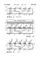
- FIG. 1illustrates an enlarged cross-sectional view of a prior art support structure 10.
- support structure 10comprises a substrate 11 having major surfaces 12 and 13.
- Metal filled vias 14extend through substrate 11 wherein one end 17 of each metal filled via 14 may terminate at surface 12 and a second end 18 of each metal filled via 14 may terminate at surface 13.
- the viasare not limited to vias extending through substrate 11, i.e., the metal filled vias 14 may terminate on interconnects, signal planes, ground planes, power planes, other metal filled vias, and the like.
- Contact pads 19are formed on major surface 12 and in contact with ends 17.
- contact or interconnect pads 21are formed on major surface 13 and in contact with second ends 18.
- structures 21are not limited to contact pads but may be conducting feedouts or electrical interconnects.
- Suitable materials for substrate 11include polyimide, FR-4, bismaleimide triazine (BT) resin, ceramic materials, and the like.
- support structure 10is a printed circuit board. Techniques for manufacturing support structures such as printed circuit boards are well known to those skilled in the art.
- FIG. 2illustrates a highly enlarged cross-sectional view of support structure 10 of FIG. 1 during irradiation by x-ray radiation in accordance with the first embodiment of the present invention. It shall be understood that the same reference numerals are used in the figures to denote the same elements. What is shown in FIG. 2 is support structure 10 having a plating base or base plate 22 formed on major surface 12 and contact pads 19. Plating base 22 provides a conductive path for the formation of probe tips (reference numeral 36 of FIG. 3) by electrodeposition. In one embodiment, plating base 22 is a two layer structure comprising an adhesion layer 20 having a plating seed layer 24 disposed thereon.
- Suitable materials for the adhesion layer 20include titanium, chromium, and the like, whereas suitable materials for plating seed layer 24 include gold, nickel, and the like.
- adhesion layer 20is titanium having a thickness of approximately 100 angstroms and plating seed layer 24 is gold having a thickness of approximately 200 angstroms.
- layers 20 and 24are not limitations of the present invention.
- layers 20 and 24are conformal layers; however, layers 20 and 24 being conformal is not a limitation of the present invention.
- the thickness of layers 20 and 24may be increased to add mechanical stability to probe tips 36 shown in FIG. 3. Further, the mechanical stability of probe tips 36 shown in FIG.
- plating base 3may be further increased by etching wells or indentations (not shown) into substrate 11 at locations where conductive pads 19 are to be formed. These wells increase the mechanical stability of the probe tips by increasing the size of the base regions of the probe tips. It should also be noted that formation of the plating base may be omitted if contact pads 19 or ends 17 of metal filled vias 14 are accessible to the cathode of the plating equipment, i.e., contact pads 19 or ends 17 serve as the plating base.
- FIG. 2illustrates an x-ray mask 26 coupled to an x-ray radiation source 27.
- x-ray radiation source 27 shown in FIG. 2emits X rays and is merely a representation of x-ray radiation sources that are well known to those skilled in the art.
- X-ray mask 26comprises a thin membrane of low atomic weight material 28 having a patterned layer of high atomic weight material 29 disposed thereon. X rays are capable of traveling through thin membrane 28 but are absorbed by the high atomic weight material 29. Thus, high atomic weight material 29 is also referred to as an absorbing material. Absorbing material 29 is patterned to have openings 31 through which x-ray radiation travels.
- Suitable materials for thin membrane 28include Si x N y , SiC, diamond, doped Si and the like, whereas suitable materials for the high atomic weight material include gold, tungsten, tantalum, and the like.
- the variables x and yare real numbers that represent atomic ratios of the constituent elements, e.g. stoichiometric silicon nitride is represented by Si 3 N 4 .
- x-ray maskssuch as x-ray mask 26 are well known in the art and the x-ray mask is not limited to a thin membrane of low atomic weight material having a patterned layer of high atomic weight material disposed thereon.
- x-ray mask 26may be a self-supporting sheet of metal having holes cut therethrough using laser ablation.
- x-ray radiation sourcessuch as source 27 are also well known to those skilled in the art.
- x-ray radiation source 27may be a synchrotron.
- Other examples of x-ray radiation sources 27include conventional metal anode x-ray tubes, plasma sources, focused laser plasma sources, and the like. It should be understood that the material for x-ray mask 26 and the type of x-ray radiation source 27 are not limitations of the present invention.
- Plating base 22is coated with a layer of resist 23 such as, for example, polymethylmethacrylate (PMMA) having a thickness ranging between approximately 50 microns ( ⁇ m) and approximately 500 ⁇ m.
- a layer of resist 23such as, for example, polymethylmethacrylate (PMMA) having a thickness ranging between approximately 50 microns ( ⁇ m) and approximately 500 ⁇ m.
- Other suitable materials for layer of resist 23include fluorinated polybutylmethacrylate, polymethacrylimide (PMI) , polyoxymethylene (POM), and polyalkensulfone (PASO) .
- PMIpolymethacrylimide
- POMpolyoxymethylene
- PASOpolyalkensulfone
- x-ray radiation source 27transmits x-ray radiation (shown by arrows 32) towards x-ray mask 26.
- x-ray radiation 32is absorbed by absorbing material 29, it travels through openings 31 and irradiates the portions of layer of resist 23 that are to be removed.
- x-ray radiation 32is transmitted at an angle so that it irradiates layer of resist 23 at an acute angle ⁇ relative to a top surface 25 of layer of resist 23.
- angle ⁇is non-normal to surface 25.
- the angle ⁇is also referred to as being an off-angle since it is oblique to surface 25.
- acute angle ⁇ranges between approximately 65 and 85 degrees.
- angle ⁇in one or both directions, i.e. vary angle ⁇ up and down, or sideways, or in a combined elliptical motion to expose a greater portion of layer of resist 23 at plating base 22 than at top surface 25.
- the exposed portions of layer of resist 23have a tapered shape having a longitudinal axis making an angle ⁇ relative to top surface 25.
- the exposing radiationhas a sufficiently short wavelength, e.g., less than approximately 5 angstroms ( ⁇ ), to penetrate the thickness of layer of resist 23 and to provide exposure of the resist down to the plating base 22.
- ⁇angstroms
- x-ray lithography in accordance with the present inventiondiffers from that used in standard integrated circuit and deep-etch lithography, electroforming, and moulding (LIGA) lithography techniques in that a reduced degree of collimation is required.
- LIGAis an acronym derived from a process described in the German language as Lithographie, Galvanoformung, Abformung. Therefore, the source and beamline of the x-ray radiation in the present invention is optimized for the intensity of radiation to reduce exposure time at the expense of coherence and source spot size.
- the exposurecan be performed at a reduced distance from the source, as compared with x-ray lithography used in the manufacture of integrated circuits.
- the intensity of radiation and the consequent rate of exposure at the resistis then increased as the inverse square of the distance to the source.
- the increased penumbra effecthelps produce the desired taper in the probe tip and thus is beneficial.
- lithographic techniques in accordance with the present inventionuse a mechanical fixture to set and to vary an oblique angle of incidence of the radiation.
- x-ray lithography for integrated circuit applicationsrequires high resolution masks and a gap of approximately 40 microns or less between mask and wafer to prevent blurring due to penumbral and diffraction effects.
- the x-ray lithographic technique in accordance with the present inventionuses a low resolution mask, wherein the gap between mask and wafer can be greater than 100 microns.
- the x-ray lithographic technique of the present inventionuses a less costly and more physically robust x-ray mask, as well as a much less costly mask-to-substrate alignment tool than conventional photolithographic techniques used for the manufacture of integrated circuits.
- the mask for the present inventioncan be manufactured by laser ablation of a 25 micron thick tungsten sheet to provide a very low cost mask with sufficient precision.
- openings 33are tapered having a greater diameter at plating base 22 than at top surface 25.
- a longitudinal axis of openings 33makes an angle ⁇ relative to plating base 22 and to top surface 25.
- probes 36are formed on support structure 10 by electroplating a conductive material on the exposed portions of plating base 22, thereby forming a probe card or probe structure 40.
- the electroplating materialfills openings 33 (shown in FIG. 2).
- Suitable electroplating materialsinclude nickel, gold, a combination of nickel and gold, copper, palladium, tin, and the like.
- a combination of layers of the electroplating materialsmay be used to enhance the strength of the base region and lower the contact resistance at the tip.
- a base 34 of probe 36may be formed by partially filling opening 33 with nickel and the tip region 35 of probe 36 may be formed by partially filling opening 33 with one of gold or palladium.
- the nickelprovides strength to probe 36, whereas the gold lowers the contact resistance between probe 36 and a structure contacted by probe 36.
- layer of resist 23is removed using techniques well known to those skilled in the art.
- portions of plating base 22 between conductive pads 19are removed to expose surface 12.
- conductive pads 19are electrically isolated from one another. Techniques for selectively removing portions of a plating base 22 are known to those skilled in the art.
- Probes 36are tapered and have a longitudinal axis that makes an acute angle ⁇ relative to plating base 22.
- the portion of probes 36 in contact with plating base 22, i.e., the base portion of probes 36have a diameter of approximately 25 ⁇ m and the portions of probe 36 that form the tip have a diameter of approximately 10 ⁇ m.
- Tapering probes 36allows them to scrub bonding pads (not shown) when contacting the bonding pads and distributes stress so that elastic compliance at the tip is maximized, while stress concentration at the base is avoided.
- Angling probes 36so that they have a longitudinal axis that makes the acute angle ⁇ provides probes 36 with compliance in both normal and lateral directions; therefore, probes 36 will contact pads with a low-force scrubbing action and accommodate pads of differing height without buckling.
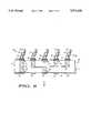
- FIG. 4illustrates an enlarged cross-sectional view of a support structure 10 (shown in FIG. 1) coated with a layer of resist 45 and being irradiated with ultraviolet radiation.
- suitable materials for layer of resist 45include commercially available novolac based resists in the longer wavelength UV range, and chemically amplified t-butoxycarbonyl (TBOC) based resists in the shorter wavelength UV range.
- layer of resist 45has a thickness ranging between approximately 10 um and approximately 60 ⁇ m. Resists for use in ultraviolet lithography are well known to those skilled in the art.
- FIG. 4illustrates a UV mask 41 coupled to a UV radiation source 42.
- UV radiation mask 41comprises a thick quartz plate 43 having a patterned layer of chromium 44 disposed thereon. UV radiation is capable of traveling through quartz plate 43 but is absorbed by chromium 44. Thus, material 44 is also referred to as an absorbing material. Absorbing material 44 is patterned to have openings 47 through which UV radiation 48 travels.
- UV maskssuch as UV mask 41 are well known in the art.
- UV radiation sources such as source 42are also well known to those skilled in the art.
- UV radiation source 27may be a mercury i-line source (lamp).
- Other examples of a UV radiation source 42include other radiation lines in the UV (lamp sources) and excimer lasers. It should be understood that the material for UV mask 41 and the type of UV radiation source 42 are not limitations of the present invention.
- UV radiation source 42transmits UV radiation (shown by arrows 48) toward UV mask 41.
- UV radiation 48is absorbed by absorbing material 44, it travels through openings 47 and irradiates the portions of layer of resist 45 that are to be removed.
- the thickness of layer of resist 45is approximately 50 microns at each exposure step to mitigate the diffraction and absorption effects of the UV radiation.
- a probe structuremay include construction in several 50 micron steps to attain the desired vertical dimension. The tapered, oblique design of the probe structure is created by selection of the sizes of mask opening 47 and alignment to previous layers at each step. The sizes and offsets of openings 47 are selected to provide the proper horizontal and vertical compliance in the final structure.
- layer of resist 45is preferably chosen for high sensitivity and low absorption of UV radiation at the expense of high resolution.
- the size of openings 47 and alignment tolerances in accordance with the present inventionare much less critical than the tolerances for conventional integrated circuit photolithographic techniques. Therefore, the cost of the masks and alignment tools is less than for conventional photolithographic techniques.
- the exposed portions of layer of resist 45are developed using a developer such as, for example, tetramethyl ammonium hydroxide (TMAH), and rinsed to form openings 49.
- a developersuch as, for example, tetramethyl ammonium hydroxide (TMAH)
- TMAHtetramethyl ammonium hydroxide
- a first portion 51 of probes 56(shown in FIG. 6) is formed by electroplating a conductive material on the exposed portions of plating base 22.
- the electroplating materialfills openings 49 (shown in FIG. 4).
- Suitable materials for electroplatinginclude nickel, gold, a combination of nickel and gold, copper, palladium, tin, and the like.
- Layer of resist 45 and first portions 51 of probe 56are covered by another layer of resist 45'.
- UV radiation source 42transmits UV radiation (shown by arrows 48) toward UV mask 41'.
- UV radiation mask 41'comprises a thick quartz plate 43' having a patterned layer of absorbing material 44' disposed thereon.
- UV radiationis capable of traveling through the thick quartz plate 43' but is absorbed by the absorbing material 44'.
- Absorbing material 44'is patterned to have openings 47' through which UV radiation travels.
- UV radiation 48is absorbed by absorbing material 44', it travels through openings 47' and irradiates the portions of layer of resist 45' that are to be removed and thereby form openings 49'.
- openings 47' of UV mask 41'are slightly offset from openings 47 of UV mask 41. This offset provides a stair-step shape for probes 56.
- the number of stepsis selected by the desired height and compressibility of probes 56. In other words, the steps of forming the portions of probe 56 may be repeated until probe 56 has the desired cross sectional profile.
- Probes 56comprise a plurality of portions 51, 51', and 51" formed on top of each other
- portions 51, 51', and 51"are formed using successive lithographic and plating steps.
- the size of each portion 51, 51', and 51"is not a limitation of the present invention.
- each successive portion 51' and 51"may be smaller or have less area than a preceding portion. In this fashion, it is possible to produce a tapered structure that has all the desirable mechanical and physical properties for use as a probe tip. Alternatively, cantilever structures can also be produced.
- layer of resist 45may be removed prior to formation of subsequent photoresist layers, i.e., 45'; layers of resist 45 and 45' may be removed in a single step; layers of resist 45 and 45' may be developed in a single step; or layers of resist may also be interleaved with separate plating base layers at each electrodeposition step.
- the portions of plating base 22 between conductive pads 19are removed to expose surface 12. In other words, conductive pads 19 are electrically isolated from one another. Techniques for selectively removing portions of a plating base 22 are known to those skilled in the art.
- probeswhich can be used in such applications as testing integrated devices and a method for their manufacture has been provided.
- One advantage of the present inventionis that the probes are fabricated using lithographic techniques, thus they can be fabricated in a peripheral array or in an area array. Accordingly, the bonding pad configuration on a semiconductor chip is not a limitation of the present invention, whether the density of bonding pads is high or low.
- Another advantage of the present inventionis that the probes are angled to provide compliance in a vertical direction. In other words, the probes of the present invention are tilted so that they can be moved in a direction normal to the surface of a probe card. Thus the probes are strong, compliant, and capable of scrubbing bonding pads on a semiconductor chip.
- the compliance of the probespermits the probes to contact bonding pads of different heights without damaging the probes or the semiconductor chip.
- Yet another advantage of the present inventionis that the probes horizontally scrub the bonding pads to provide electrical contact between the probes and the bonding pads due to horizontal compliance. Further, probes manufactured in accordance with the present invention permit repeatable make and break contact with bonding pads.
Landscapes
- Engineering & Computer Science (AREA)
- Manufacturing & Machinery (AREA)
- Microelectronics & Electronic Packaging (AREA)
- Physics & Mathematics (AREA)
- General Physics & Mathematics (AREA)
- Measuring Leads Or Probes (AREA)
- Testing Or Measuring Of Semiconductors Or The Like (AREA)
Abstract
Description
Claims (17)
Priority Applications (1)
| Application Number | Priority Date | Filing Date | Title |
|---|---|---|---|
| US08/293,365US5513430A (en) | 1994-08-19 | 1994-08-19 | Method for manufacturing a probe |
Applications Claiming Priority (1)
| Application Number | Priority Date | Filing Date | Title |
|---|---|---|---|
| US08/293,365US5513430A (en) | 1994-08-19 | 1994-08-19 | Method for manufacturing a probe |
Publications (1)
| Publication Number | Publication Date |
|---|---|
| US5513430Atrue US5513430A (en) | 1996-05-07 |
Family
ID=23128785
Family Applications (1)
| Application Number | Title | Priority Date | Filing Date |
|---|---|---|---|
| US08/293,365Expired - Fee RelatedUS5513430A (en) | 1994-08-19 | 1994-08-19 | Method for manufacturing a probe |
Country Status (1)
| Country | Link |
|---|---|
| US (1) | US5513430A (en) |
Cited By (103)
| Publication number | Priority date | Publication date | Assignee | Title |
|---|---|---|---|---|
| US5691210A (en)* | 1995-10-09 | 1997-11-25 | Nitto Denko Corporation | Method for fabrication of probe structure and circuit substrate therefor |
| US5843798A (en)* | 1994-01-28 | 1998-12-01 | Fujitsu Limited | Method for manufacturing semiconductor device having step of forming electrode pins on semiconductor chip using electrode-pin forming mask, and method for testing semiconductor chip using electrode-pin forming mask |
| US5886877A (en)* | 1995-10-13 | 1999-03-23 | Meiko Electronics Co., Ltd. | Circuit board, manufacturing method therefor, and bump-type contact head and semiconductor component packaging module using the circuit board |
| US5914218A (en)* | 1995-06-07 | 1999-06-22 | Xerox Corporation | Method for forming a spring contact |
| US6032356A (en)* | 1993-11-16 | 2000-03-07 | Formfactor. Inc. | Wafer-level test and burn-in, and semiconductor process |
| US6213789B1 (en) | 1999-12-15 | 2001-04-10 | Xerox Corporation | Method and apparatus for interconnecting devices using an adhesive |
| US20010012739A1 (en)* | 1997-03-17 | 2001-08-09 | Grube Gary W. | Composite microelectronic spring structure and method for making same |
| US20010028102A1 (en)* | 2000-04-10 | 2001-10-11 | Hans-Jurgen Hacke | Electronic component having microscopically small contact areas and method for fabricating it |
| US6359454B1 (en) | 1999-08-03 | 2002-03-19 | Advantest Corp. | Pick and place mechanism for contactor |
| US6379871B1 (en)* | 1998-06-10 | 2002-04-30 | Nec Corporation | Method for fabricating a mask for a LIGA process |
| US6420884B1 (en) | 1999-01-29 | 2002-07-16 | Advantest Corp. | Contact structure formed by photolithography process |
| US6426638B1 (en) | 2000-05-02 | 2002-07-30 | Decision Track Llc | Compliant probe apparatus |
| US6442831B1 (en)* | 1993-11-16 | 2002-09-03 | Formfactor, Inc. | Method for shaping spring elements |
| US6475822B2 (en) | 1993-11-16 | 2002-11-05 | Formfactor, Inc. | Method of making microelectronic contact structures |
| US6491968B1 (en) | 1998-12-02 | 2002-12-10 | Formfactor, Inc. | Methods for making spring interconnect structures |
| US6495019B1 (en) | 2000-04-19 | 2002-12-17 | Agere Systems Inc. | Device comprising micromagnetic components for power applications and process for forming device |
| US6499216B1 (en) | 1994-07-07 | 2002-12-31 | Tessera, Inc. | Methods and structures for electronic probing arrays |
| US20030025172A1 (en)* | 2001-07-11 | 2003-02-06 | Formfactor, Inc. | Method of manufacturing a probe card |
| US6520778B1 (en) | 1997-02-18 | 2003-02-18 | Formfactor, Inc. | Microelectronic contact structures, and methods of making same |
| US20030038647A1 (en)* | 1995-11-09 | 2003-02-27 | Eldridge Benjamin N. | Probe card for probing wafers with raised contact elements |
| US6530148B1 (en)* | 1999-03-08 | 2003-03-11 | Kulicke And Soffa Investments, Inc. | Method for making a probe apparatus for testing integrated circuits |
| US20030099737A1 (en)* | 1999-07-30 | 2003-05-29 | Formfactor, Inc. | Forming tool for forming a contoured microelectronic spring mold |
| US6586955B2 (en) | 2000-03-13 | 2003-07-01 | Tessera, Inc. | Methods and structures for electronic probing arrays |
| EP1160576A3 (en)* | 2000-06-01 | 2003-07-23 | Sumitomo Electric Industries, Ltd. | Contact probe and fabrication method thereof |
| US6604395B2 (en) | 2001-07-23 | 2003-08-12 | St Assembly Test Services Ltd. | Semi-automated probe bender |
| US6616966B2 (en) | 1998-12-02 | 2003-09-09 | Formfactor, Inc. | Method of making lithographic contact springs |
| US6615485B2 (en)* | 1993-11-16 | 2003-09-09 | Formfactor, Inc. | Probe card assembly and kit, and methods of making same |
| US6624648B2 (en) | 1993-11-16 | 2003-09-23 | Formfactor, Inc. | Probe card assembly |
| US20030199179A1 (en)* | 1993-11-16 | 2003-10-23 | Formfactor, Inc. | Contact tip structure for microelectronic interconnection elements and method of making same |
| US20030222668A1 (en)* | 2002-03-13 | 2003-12-04 | Scs Hightech, Inc. | Method for producing micro probe tips |
| US20040018752A1 (en)* | 2002-02-05 | 2004-01-29 | Oug-Ki Lee | Method for manufacturing electrical contact element for testing electro device and electrical contact element thereby |
| US6690186B2 (en) | 1994-07-07 | 2004-02-10 | Tessera, Inc. | Methods and structures for electronic probing arrays |
| US6713374B2 (en) | 1999-07-30 | 2004-03-30 | Formfactor, Inc. | Interconnect assemblies and methods |
| US20040072452A1 (en)* | 1998-02-13 | 2004-04-15 | Formfactor, Inc. | Microelectronic contact structures, and methods of making same |
| US20040075454A1 (en)* | 2001-01-29 | 2004-04-22 | Yoshihiro Hirata | Contact probe, method of manufacturing the contact probe, and device and method for inspection |
| US20040099641A1 (en)* | 2002-11-25 | 2004-05-27 | Formfactor, Inc. | Probe array and method of its manufacture |
| US20040104739A1 (en)* | 2001-04-13 | 2004-06-03 | Tsuyoshi Haga | Contact probe |
| US20040121627A1 (en)* | 2002-12-23 | 2004-06-24 | Formfactor, Inc. | Microelectronic contact structure |
| US20040124867A1 (en)* | 2000-07-13 | 2004-07-01 | International Business Machines Corporation | Tfi probe i/o wrap test method |
| US6759311B2 (en) | 2001-10-31 | 2004-07-06 | Formfactor, Inc. | Fan out of interconnect elements attached to semiconductor wafer |
| US6763578B2 (en)* | 1988-09-30 | 2004-07-20 | Micron Technology, Inc. | Method and apparatus for manufacturing known good semiconductor die |
| US6791176B2 (en) | 1998-12-02 | 2004-09-14 | Formfactor, Inc. | Lithographic contact elements |
| US6811406B2 (en) | 2001-04-12 | 2004-11-02 | Formfactor, Inc. | Microelectronic spring with additional protruding member |
| US20040217767A1 (en)* | 2003-05-01 | 2004-11-04 | Diorio Mark L. | Wafer probing that conditions devices for flip-chip bonding |
| US6836962B2 (en) | 1993-11-16 | 2005-01-04 | Formfactor, Inc. | Method and apparatus for shaping spring elements |
| US6888362B2 (en) | 2000-11-09 | 2005-05-03 | Formfactor, Inc. | Test head assembly for electronic components with plurality of contoured microelectronic spring contacts |
| US20050104609A1 (en)* | 2003-02-04 | 2005-05-19 | Microfabrica Inc. | Microprobe tips and methods for making |
| US20050146339A1 (en)* | 2001-07-11 | 2005-07-07 | Formfactor, Inc. | Method of manufacturing a probe card |
| KR100502125B1 (en)* | 1999-06-28 | 2005-07-19 | 가부시키가이샤 어드밴티스트 | Method of producing a contact structure |
| US20050179456A1 (en)* | 1996-03-12 | 2005-08-18 | Beaman Brian S. | High density cantilevered probe for electronic devices |
| KR100508419B1 (en)* | 1999-04-30 | 2005-08-18 | 가부시키가이샤 어드밴티스트 | Contact structure formed by microfabrication process |
| US20050189959A1 (en)* | 2003-02-04 | 2005-09-01 | Microfabrica Inc. | Electrochemical fabrication process for forming multilayer multimaterial microprobe structures |
| US6939474B2 (en) | 1999-07-30 | 2005-09-06 | Formfactor, Inc. | Method for forming microelectronic spring structures on a substrate |
| US20050221644A1 (en)* | 2003-02-04 | 2005-10-06 | Kieun Kim | Microprobe tips and methods for making |
| WO2005010927A3 (en)* | 2003-07-18 | 2005-10-20 | Commissariat Energie Atomique | Anisotropic electroconductive film and method for the production thereof |
| US20060027899A1 (en)* | 2004-06-25 | 2006-02-09 | Tessera, Inc. | Structure with spherical contact pins |
| US20060051948A1 (en)* | 2003-02-04 | 2006-03-09 | Microfabrica Inc. | Microprobe tips and methods for making |
| US20060053625A1 (en)* | 2002-05-07 | 2006-03-16 | Microfabrica Inc. | Microprobe tips and methods for making |
| US20060112550A1 (en)* | 2002-05-07 | 2006-06-01 | Microfabrica Inc. | Microprobe tips and methods for making |
| US7073254B2 (en)* | 1993-11-16 | 2006-07-11 | Formfactor, Inc. | Method for mounting a plurality of spring contact elements |
| US20060286829A1 (en)* | 2003-02-04 | 2006-12-21 | Microfabrica Inc. | Microprobe tips and methods for making |
| US20070024298A1 (en)* | 2005-08-01 | 2007-02-01 | Touchdown Technologies, Inc. | Torsion spring probe contactor design |
| US20070024297A1 (en)* | 2005-08-01 | 2007-02-01 | Touchdown Technologies, Inc. | Post and tip design for a probe contact |
| WO2007021046A1 (en)* | 2005-08-19 | 2007-02-22 | Microfriend Inc. | Method of manufacturing needle for probe card using fine processing technology, needle manufactured by the method, and probe card comprising the needle |
| WO2007026985A1 (en)* | 2005-08-31 | 2007-03-08 | Microfriend Inc. | Method for fabricating probe needle tip of probe card |
| US7189077B1 (en) | 1999-07-30 | 2007-03-13 | Formfactor, Inc. | Lithographic type microelectronic spring structures with improved contours |
| US20070176619A1 (en)* | 1993-11-16 | 2007-08-02 | Formfactor, Inc. | Probe For Semiconductor Devices |
| US20070259456A1 (en)* | 2006-05-02 | 2007-11-08 | Formfactor, Inc. | Extended Probe Tips |
| US20080048688A1 (en)* | 2000-03-17 | 2008-02-28 | Formfactor, Inc. | Methods for planarizing a semiconductor contactor |
| US20080108221A1 (en)* | 2003-12-31 | 2008-05-08 | Microfabrica Inc. | Microprobe Tips and Methods for Making |
| US7371072B2 (en) | 1998-12-02 | 2008-05-13 | Formfactor, Inc. | Spring interconnect structures |
| US7435108B1 (en)* | 1999-07-30 | 2008-10-14 | Formfactor, Inc. | Variable width resilient conductive contact structures |
| US20080278185A1 (en)* | 2007-05-09 | 2008-11-13 | Mjc Probe Incorporation | Electrical contact device and its manufacturing process |
| US7553165B2 (en) | 1998-12-02 | 2009-06-30 | Formfactor, Inc. | Spring interconnect structures |
| US20090256583A1 (en)* | 2003-02-04 | 2009-10-15 | Microfabrica Inc. | Vertical Microprobes for Contacting Electronic Components and Method for Making Such Probes |
| US20090320990A1 (en)* | 2003-02-04 | 2009-12-31 | Microfabrica Inc. | Electrochemical Fabrication Process for Forming Multilayer Multimaterial Microprobe Structures |
| US20100038126A1 (en)* | 2004-07-30 | 2010-02-18 | International Business Machines Corporation | Interposer structures and methods of manufacturing the same |
| US7714235B1 (en) | 1997-05-06 | 2010-05-11 | Formfactor, Inc. | Lithographically defined microelectronic contact structures |
| US20100134131A1 (en)* | 2003-02-04 | 2010-06-03 | Microfabrica Inc. | Electrochemically Fabricated Microprobes |
| US20100144216A1 (en)* | 2004-10-27 | 2010-06-10 | Jurgen Daniel | Oblique Parts or Surfaces |
| US20100203721A1 (en)* | 2002-08-29 | 2010-08-12 | Hiatt William M | Multi-component integrated circuit contacts |
| US20110057018A1 (en)* | 1995-05-26 | 2011-03-10 | Formfactor, Inc. | Method of wirebonding that utilizes a gas flow within a capillary from which a wire is played out |
| US20110132767A1 (en)* | 2003-02-04 | 2011-06-09 | Microfabrica Inc. | Multi-Layer, Multi-Material Fabrication Methods for Producing Micro-Scale and Millimeter-Scale Devices with Enhanced Electrical and/or Mechanical Properties |
| US8033838B2 (en) | 1996-02-21 | 2011-10-11 | Formfactor, Inc. | Microelectronic contact structure |
| US20120003851A1 (en)* | 2010-06-29 | 2012-01-05 | Molex Incorporated | Sheet-Like Connector And Manufacturing Method Thereof |
| US20120098562A1 (en)* | 2010-10-21 | 2012-04-26 | Brymen Technology Corporation | Probe tip coating structure for test probes |
| US8373428B2 (en) | 1993-11-16 | 2013-02-12 | Formfactor, Inc. | Probe card assembly and kit, and methods of making same |
| US8717055B2 (en) | 2003-02-04 | 2014-05-06 | Microfabrica Inc. | Probe devices formed from multiple planar layers of structural material with tip regions formed from one or more intermediate planar layers |
| US9671429B2 (en) | 2003-05-07 | 2017-06-06 | University Of Southern California | Multi-layer, multi-material micro-scale and millimeter-scale devices with enhanced electrical and/or mechanical properties |
| US10416192B2 (en) | 2003-02-04 | 2019-09-17 | Microfabrica Inc. | Cantilever microprobes for contacting electronic components |
| US10641792B2 (en) | 2003-12-31 | 2020-05-05 | University Of Southern California | Multi-layer, multi-material micro-scale and millimeter-scale devices with enhanced electrical and/or mechanical properties |
| US20220026466A1 (en)* | 2010-05-12 | 2022-01-27 | Stmicroelectronics S.R.L. | Probes for testing integrated electronic circuits and corresponding production method |
| US11262383B1 (en) | 2018-09-26 | 2022-03-01 | Microfabrica Inc. | Probes having improved mechanical and/or electrical properties for making contact between electronic circuit elements and methods for making |
| US11761982B1 (en) | 2019-12-31 | 2023-09-19 | Microfabrica Inc. | Probes with planar unbiased spring elements for electronic component contact and methods for making such probes |
| US11774467B1 (en) | 2020-09-01 | 2023-10-03 | Microfabrica Inc. | Method of in situ modulation of structural material properties and/or template shape |
| US11802891B1 (en) | 2019-12-31 | 2023-10-31 | Microfabrica Inc. | Compliant pin probes with multiple spring segments and compression spring deflection stabilization structures, methods for making, and methods for using |
| US11973301B2 (en) | 2018-09-26 | 2024-04-30 | Microfabrica Inc. | Probes having improved mechanical and/or electrical properties for making contact between electronic circuit elements and methods for making |
| US12000865B2 (en) | 2019-02-14 | 2024-06-04 | Microfabrica Inc. | Multi-beam vertical probes with independent arms formed of a high conductivity metal for enhancing current carrying capacity and methods for making such probes |
| US12078657B2 (en) | 2019-12-31 | 2024-09-03 | Microfabrica Inc. | Compliant pin probes with extension springs, methods for making, and methods for using |
| US12146898B2 (en) | 2020-10-02 | 2024-11-19 | Microfabrica Inc. | Multi-beam probes with decoupled structural and current carrying beams and methods of making |
| US12181493B2 (en) | 2018-10-26 | 2024-12-31 | Microfabrica Inc. | Compliant probes including dual independently operable probe contact elements including at least one flat extension spring, methods for making, and methods for using |
| US12196781B2 (en) | 2019-12-31 | 2025-01-14 | Microfabrica Inc. | Probes with planar unbiased spring elements for electronic component contact, methods for making such probes, and methods for using such probes |
| US12196782B2 (en) | 2019-12-31 | 2025-01-14 | Microfabrica Inc. | Probes with planar unbiased spring elements for electronic component contact, methods for making such probes, and methods for using such probes |
Citations (11)
| Publication number | Priority date | Publication date | Assignee | Title |
|---|---|---|---|---|
| US3445770A (en)* | 1965-12-27 | 1969-05-20 | Philco Ford Corp | Microelectronic test probe with defect marker access |
| US3905098A (en)* | 1973-08-09 | 1975-09-16 | Xynetics Inc | Microelectronic test probe card including a multiplicity of probe contacts and method of making same |
| US4563640A (en)* | 1981-06-03 | 1986-01-07 | Yoshiei Hasegawa | Fixed probe board |
| US4924589A (en)* | 1988-05-16 | 1990-05-15 | Leedy Glenn J | Method of making and testing an integrated circuit |
| EP0368262A2 (en)* | 1988-11-09 | 1990-05-16 | Nitto Denko Corporation | Wiring substrate, film carrier, semiconductor device made by using the film carrier, and mounting structure comprising the semiconductor device |
| US5020219A (en)* | 1988-05-16 | 1991-06-04 | Leedy Glenn J | Method of making a flexible tester surface for testing integrated circuits |
| US5042148A (en)* | 1989-10-11 | 1991-08-27 | Mitsubishi Denki Kabushiki Kaisha | Method of manufacturing a probing card for wafer testing |
| US5060371A (en)* | 1988-10-05 | 1991-10-29 | Applied Precision, Inc. | Method of making probe cards |
| US5090118A (en)* | 1990-07-31 | 1992-02-25 | Texas Instruments Incorporated | High performance test head and method of making |
| US5103557A (en)* | 1988-05-16 | 1992-04-14 | Leedy Glenn J | Making and testing an integrated circuit using high density probe points |
| US5191708A (en)* | 1990-06-20 | 1993-03-09 | Hitachi, Ltd. | Manufacturing method of a probe head for semiconductor LSI inspection apparatus |
- 1994
- 1994-08-19USUS08/293,365patent/US5513430A/ennot_activeExpired - Fee Related
Patent Citations (11)
| Publication number | Priority date | Publication date | Assignee | Title |
|---|---|---|---|---|
| US3445770A (en)* | 1965-12-27 | 1969-05-20 | Philco Ford Corp | Microelectronic test probe with defect marker access |
| US3905098A (en)* | 1973-08-09 | 1975-09-16 | Xynetics Inc | Microelectronic test probe card including a multiplicity of probe contacts and method of making same |
| US4563640A (en)* | 1981-06-03 | 1986-01-07 | Yoshiei Hasegawa | Fixed probe board |
| US4924589A (en)* | 1988-05-16 | 1990-05-15 | Leedy Glenn J | Method of making and testing an integrated circuit |
| US5020219A (en)* | 1988-05-16 | 1991-06-04 | Leedy Glenn J | Method of making a flexible tester surface for testing integrated circuits |
| US5103557A (en)* | 1988-05-16 | 1992-04-14 | Leedy Glenn J | Making and testing an integrated circuit using high density probe points |
| US5060371A (en)* | 1988-10-05 | 1991-10-29 | Applied Precision, Inc. | Method of making probe cards |
| EP0368262A2 (en)* | 1988-11-09 | 1990-05-16 | Nitto Denko Corporation | Wiring substrate, film carrier, semiconductor device made by using the film carrier, and mounting structure comprising the semiconductor device |
| US5042148A (en)* | 1989-10-11 | 1991-08-27 | Mitsubishi Denki Kabushiki Kaisha | Method of manufacturing a probing card for wafer testing |
| US5191708A (en)* | 1990-06-20 | 1993-03-09 | Hitachi, Ltd. | Manufacturing method of a probe head for semiconductor LSI inspection apparatus |
| US5090118A (en)* | 1990-07-31 | 1992-02-25 | Texas Instruments Incorporated | High performance test head and method of making |
Non-Patent Citations (4)
| Title |
|---|
| C. Barsotti et al., "Very High Density Probing", 1988 International Test Conference, Paper 30.2, pp. 608-614. |
| C. Barsotti et al., Very High Density Probing , 1988 International Test Conference, Paper 30.2, pp. 608 614.* |
| Munchmeyer et al., "Manufacture of three-dimensional microdevices using synchrotron radiation (invited)", Rev. Sci Instrum. 63(1), Jan. 1992, pp. 713-721. |
| Munchmeyer et al., Manufacture of three dimensional microdevices using synchrotron radiation (invited) , Rev. Sci Instrum. 63(1), Jan. 1992, pp. 713 721.* |
Cited By (221)
| Publication number | Priority date | Publication date | Assignee | Title |
|---|---|---|---|---|
| US6763578B2 (en)* | 1988-09-30 | 2004-07-20 | Micron Technology, Inc. | Method and apparatus for manufacturing known good semiconductor die |
| US6442831B1 (en)* | 1993-11-16 | 2002-09-03 | Formfactor, Inc. | Method for shaping spring elements |
| US6475822B2 (en) | 1993-11-16 | 2002-11-05 | Formfactor, Inc. | Method of making microelectronic contact structures |
| US6624648B2 (en) | 1993-11-16 | 2003-09-23 | Formfactor, Inc. | Probe card assembly |
| US6032356A (en)* | 1993-11-16 | 2000-03-07 | Formfactor. Inc. | Wafer-level test and burn-in, and semiconductor process |
| US20070046313A1 (en)* | 1993-11-16 | 2007-03-01 | Formfactor, Inc. | Mounting Spring Elements on Semiconductor Devices, and Wafer-Level Testing Methodology |
| US20030199179A1 (en)* | 1993-11-16 | 2003-10-23 | Formfactor, Inc. | Contact tip structure for microelectronic interconnection elements and method of making same |
| US6655023B1 (en) | 1993-11-16 | 2003-12-02 | Formfactor, Inc. | Method and apparatus for burning-in semiconductor devices in wafer form |
| US6836962B2 (en) | 1993-11-16 | 2005-01-04 | Formfactor, Inc. | Method and apparatus for shaping spring elements |
| US20070176619A1 (en)* | 1993-11-16 | 2007-08-02 | Formfactor, Inc. | Probe For Semiconductor Devices |
| US8373428B2 (en) | 1993-11-16 | 2013-02-12 | Formfactor, Inc. | Probe card assembly and kit, and methods of making same |
| US7142000B2 (en) | 1993-11-16 | 2006-11-28 | Formfactor, Inc. | Mounting spring elements on semiconductor devices, and wafer-level testing methodology |
| US6701612B2 (en) | 1993-11-16 | 2004-03-09 | Formfactor, Inc. | Method and apparatus for shaping spring elements |
| US7601039B2 (en) | 1993-11-16 | 2009-10-13 | Formfactor, Inc. | Microelectronic contact structure and method of making same |
| US6615485B2 (en)* | 1993-11-16 | 2003-09-09 | Formfactor, Inc. | Probe card assembly and kit, and methods of making same |
| US6482013B2 (en) | 1993-11-16 | 2002-11-19 | Formfactor, Inc. | Microelectronic spring contact element and electronic component having a plurality of spring contact elements |
| US7086149B2 (en)* | 1993-11-16 | 2006-08-08 | Formfactor, Inc. | Method of making a contact structure with a distinctly formed tip structure |
| US7073254B2 (en)* | 1993-11-16 | 2006-07-11 | Formfactor, Inc. | Method for mounting a plurality of spring contact elements |
| US5843798A (en)* | 1994-01-28 | 1998-12-01 | Fujitsu Limited | Method for manufacturing semiconductor device having step of forming electrode pins on semiconductor chip using electrode-pin forming mask, and method for testing semiconductor chip using electrode-pin forming mask |
| US6690186B2 (en) | 1994-07-07 | 2004-02-10 | Tessera, Inc. | Methods and structures for electronic probing arrays |
| US6499216B1 (en) | 1994-07-07 | 2002-12-31 | Tessera, Inc. | Methods and structures for electronic probing arrays |
| US20110057018A1 (en)* | 1995-05-26 | 2011-03-10 | Formfactor, Inc. | Method of wirebonding that utilizes a gas flow within a capillary from which a wire is played out |
| US8485418B2 (en) | 1995-05-26 | 2013-07-16 | Formfactor, Inc. | Method of wirebonding that utilizes a gas flow within a capillary from which a wire is played out |
| US6184065B1 (en) | 1995-06-07 | 2001-02-06 | Xerox Corporation | Photolithographically patterned spring contact |
| US5914218A (en)* | 1995-06-07 | 1999-06-22 | Xerox Corporation | Method for forming a spring contact |
| US5691210A (en)* | 1995-10-09 | 1997-11-25 | Nitto Denko Corporation | Method for fabrication of probe structure and circuit substrate therefor |
| US5886877A (en)* | 1995-10-13 | 1999-03-23 | Meiko Electronics Co., Ltd. | Circuit board, manufacturing method therefor, and bump-type contact head and semiconductor component packaging module using the circuit board |
| US6350957B1 (en)* | 1995-10-13 | 2002-02-26 | Meiko Electronics, Co., Ltd. | Circuit board, manufacturing method therefor, and bump-type contact head and semiconductor component packaging module using the circuit board |
| US6239983B1 (en)* | 1995-10-13 | 2001-05-29 | Meiko Electronics Co., Ltd. | Circuit board, manufacturing method therefor, and bump-type contact head and semiconductor component packaging module using the circuit board |
| US6937037B2 (en) | 1995-11-09 | 2005-08-30 | Formfactor, Et Al. | Probe card assembly for contacting a device with raised contact elements |
| US20030038647A1 (en)* | 1995-11-09 | 2003-02-27 | Eldridge Benjamin N. | Probe card for probing wafers with raised contact elements |
| US8033838B2 (en) | 1996-02-21 | 2011-10-11 | Formfactor, Inc. | Microelectronic contact structure |
| US7332922B2 (en)* | 1996-03-12 | 2008-02-19 | International Business Machines Corporation | Method for fabricating a structure for making contact with a device |
| US20050179456A1 (en)* | 1996-03-12 | 2005-08-18 | Beaman Brian S. | High density cantilevered probe for electronic devices |
| US20080030215A1 (en)* | 1996-03-12 | 2008-02-07 | Beaman Brian S | High density cantilevered probe for electronic devices |
| US6520778B1 (en) | 1997-02-18 | 2003-02-18 | Formfactor, Inc. | Microelectronic contact structures, and methods of making same |
| US20010012739A1 (en)* | 1997-03-17 | 2001-08-09 | Grube Gary W. | Composite microelectronic spring structure and method for making same |
| US7063541B2 (en)* | 1997-03-17 | 2006-06-20 | Formfactor, Inc. | Composite microelectronic spring structure and method for making same |
| US7714235B1 (en) | 1997-05-06 | 2010-05-11 | Formfactor, Inc. | Lithographically defined microelectronic contact structures |
| US20040072452A1 (en)* | 1998-02-13 | 2004-04-15 | Formfactor, Inc. | Microelectronic contact structures, and methods of making same |
| US20090286429A1 (en)* | 1998-02-13 | 2009-11-19 | Formfactor, Inc. | Microelectronic contact structures, and methods of making same |
| US6807734B2 (en) | 1998-02-13 | 2004-10-26 | Formfactor, Inc. | Microelectronic contact structures, and methods of making same |
| US7798822B2 (en) | 1998-02-13 | 2010-09-21 | Formfactor, Inc. | Microelectronic contact structures |
| US6379871B1 (en)* | 1998-06-10 | 2002-04-30 | Nec Corporation | Method for fabricating a mask for a LIGA process |
| US6491968B1 (en) | 1998-12-02 | 2002-12-10 | Formfactor, Inc. | Methods for making spring interconnect structures |
| US20100088888A1 (en)* | 1998-12-02 | 2010-04-15 | Formfactor, Inc. | Lithographic contact elements |
| US7555836B2 (en) | 1998-12-02 | 2009-07-07 | Formfactor, Inc. | Method of making lithographic contact elements |
| US7287322B2 (en) | 1998-12-02 | 2007-10-30 | Formfactor, Inc. | Lithographic contact elements |
| US6791176B2 (en) | 1998-12-02 | 2004-09-14 | Formfactor, Inc. | Lithographic contact elements |
| US7841863B2 (en) | 1998-12-02 | 2010-11-30 | Formfactor, Inc. | Spring interconnect structures |
| US20050148214A1 (en)* | 1998-12-02 | 2005-07-07 | Formfactor, Inc. | Lithographic contact elements |
| US7553165B2 (en) | 1998-12-02 | 2009-06-30 | Formfactor, Inc. | Spring interconnect structures |
| US7371072B2 (en) | 1998-12-02 | 2008-05-13 | Formfactor, Inc. | Spring interconnect structures |
| US20080115353A1 (en)* | 1998-12-02 | 2008-05-22 | Formfactor, Inc. | Lithographic contact elements |
| US6616966B2 (en) | 1998-12-02 | 2003-09-09 | Formfactor, Inc. | Method of making lithographic contact springs |
| US6420884B1 (en) | 1999-01-29 | 2002-07-16 | Advantest Corp. | Contact structure formed by photolithography process |
| US6530148B1 (en)* | 1999-03-08 | 2003-03-11 | Kulicke And Soffa Investments, Inc. | Method for making a probe apparatus for testing integrated circuits |
| KR100508419B1 (en)* | 1999-04-30 | 2005-08-18 | 가부시키가이샤 어드밴티스트 | Contact structure formed by microfabrication process |
| KR100502125B1 (en)* | 1999-06-28 | 2005-07-19 | 가부시키가이샤 어드밴티스트 | Method of producing a contact structure |
| US6939474B2 (en) | 1999-07-30 | 2005-09-06 | Formfactor, Inc. | Method for forming microelectronic spring structures on a substrate |
| US7675301B2 (en)* | 1999-07-30 | 2010-03-09 | Formfactor, Inc. | Electronic components with plurality of contoured microelectronic spring contacts |
| US7189077B1 (en) | 1999-07-30 | 2007-03-13 | Formfactor, Inc. | Lithographic type microelectronic spring structures with improved contours |
| US6713374B2 (en) | 1999-07-30 | 2004-03-30 | Formfactor, Inc. | Interconnect assemblies and methods |
| US7435108B1 (en)* | 1999-07-30 | 2008-10-14 | Formfactor, Inc. | Variable width resilient conductive contact structures |
| US6780001B2 (en) | 1999-07-30 | 2004-08-24 | Formfactor, Inc. | Forming tool for forming a contoured microelectronic spring mold |
| US20050016251A1 (en)* | 1999-07-30 | 2005-01-27 | Formfactor, Inc. | Forming tool for forming a contoured microelectronic spring mold |
| US20030099737A1 (en)* | 1999-07-30 | 2003-05-29 | Formfactor, Inc. | Forming tool for forming a contoured microelectronic spring mold |
| US20060019027A1 (en)* | 1999-07-30 | 2006-01-26 | Formfactor, Inc. | Method for forming microelectronic spring structures on a substrate |
| US20070269997A1 (en)* | 1999-07-30 | 2007-11-22 | Formfactor, Inc. | Electronic components with plurality of contoured microelectronic spring contacts |
| US20090035959A1 (en)* | 1999-07-30 | 2009-02-05 | Formfactor, Inc. | Interconnect assemblies and methods |
| US7524194B2 (en) | 1999-07-30 | 2009-04-28 | Formfactor, Inc. | Lithographic type microelectronic spring structures with improved contours |
| US6359454B1 (en) | 1999-08-03 | 2002-03-19 | Advantest Corp. | Pick and place mechanism for contactor |
| US6439898B2 (en) | 1999-12-15 | 2002-08-27 | Xerox Corporation | Method and apparatus for interconnecting devices using an adhesive |
| US6213789B1 (en) | 1999-12-15 | 2001-04-10 | Xerox Corporation | Method and apparatus for interconnecting devices using an adhesive |
| US6586955B2 (en) | 2000-03-13 | 2003-07-01 | Tessera, Inc. | Methods and structures for electronic probing arrays |
| US20110193583A1 (en)* | 2000-03-17 | 2011-08-11 | Formfactor, Inc. | Methods for planarizing a semiconductor contactor |
| US20080048688A1 (en)* | 2000-03-17 | 2008-02-28 | Formfactor, Inc. | Methods for planarizing a semiconductor contactor |
| US8427183B2 (en) | 2000-03-17 | 2013-04-23 | Formfactor, Inc. | Probe card assembly having an actuator for bending the probe substrate |
| US7737709B2 (en) | 2000-03-17 | 2010-06-15 | Formfactor, Inc. | Methods for planarizing a semiconductor contactor |
| US20100263432A1 (en)* | 2000-03-17 | 2010-10-21 | Formfactor, Inc. | Methods for planarizing a semiconductor contactor |
| US20050255633A1 (en)* | 2000-04-10 | 2005-11-17 | Infineon Technologies Ag | Methods for producing an electronic device having microscopically small contact areas |
| US6946725B2 (en) | 2000-04-10 | 2005-09-20 | Infineon Technologies Ag | Electronic device having microscopically small contact areas and methods for producing the electronic device |
| DE10017746B4 (en)* | 2000-04-10 | 2005-10-13 | Infineon Technologies Ag | Method for producing an electronic component with microscopically small contact surfaces |
| US20010028102A1 (en)* | 2000-04-10 | 2001-10-11 | Hans-Jurgen Hacke | Electronic component having microscopically small contact areas and method for fabricating it |
| US6495019B1 (en) | 2000-04-19 | 2002-12-17 | Agere Systems Inc. | Device comprising micromagnetic components for power applications and process for forming device |
| US6624498B2 (en) | 2000-04-19 | 2003-09-23 | Agere Systems Inc. | Micromagnetic device having alloy of cobalt, phosphorus and iron |
| US20020180473A1 (en)* | 2000-05-02 | 2002-12-05 | Decision Track Llc | Single-sided compliant probe apparatus |
| US20040246010A1 (en)* | 2000-05-02 | 2004-12-09 | Decision Track Llc (A Limited Liability Corporation Of The State Of California) | Probe tip in single-sided compliant probe apparatus |
| US6426638B1 (en) | 2000-05-02 | 2002-07-30 | Decision Track Llc | Compliant probe apparatus |
| US6771084B2 (en) | 2000-05-02 | 2004-08-03 | Decision Track Llc | Single-sided compliant probe apparatus |
| US6617865B2 (en) | 2000-05-02 | 2003-09-09 | Decision Track Llc | Compliant probe apparatus |
| KR100808325B1 (en)* | 2000-06-01 | 2008-02-27 | 스미토모덴키고교가부시키가이샤 | Contact probe and fabrication method thereof |
| EP1160576A3 (en)* | 2000-06-01 | 2003-07-23 | Sumitomo Electric Industries, Ltd. | Contact probe and fabrication method thereof |
| US6784680B2 (en) | 2000-06-01 | 2004-08-31 | Sumitomo Electric Industries, Ltd. | Contact probe with guide unit and fabrication method thereof |
| US20030210063A1 (en)* | 2000-06-01 | 2003-11-13 | Sumitomo Electric Industries, Ltd. | Contact probe with guide unit and fabrication method thereof |
| US20040124867A1 (en)* | 2000-07-13 | 2004-07-01 | International Business Machines Corporation | Tfi probe i/o wrap test method |
| US7007380B2 (en)* | 2000-07-13 | 2006-03-07 | International Business Machines Corporation | TFI probe I/O wrap test method |
| US6888362B2 (en) | 2000-11-09 | 2005-05-03 | Formfactor, Inc. | Test head assembly for electronic components with plurality of contoured microelectronic spring contacts |
| US20050189956A1 (en)* | 2000-11-09 | 2005-09-01 | Formfactor, Inc. | Electronic components with plurality of contoured microelectronic spring contacts |
| US7245137B2 (en) | 2000-11-09 | 2007-07-17 | Formfactor, Inc. | Test head assembly having paired contact structures |
| US20040075454A1 (en)* | 2001-01-29 | 2004-04-22 | Yoshihiro Hirata | Contact probe, method of manufacturing the contact probe, and device and method for inspection |
| US7151385B2 (en)* | 2001-01-29 | 2006-12-19 | Sumitomo Electric Industries, Ltd. | Contact probe, method of manufacturing the contact probe, and device and method for inspection |
| US6811406B2 (en) | 2001-04-12 | 2004-11-02 | Formfactor, Inc. | Microelectronic spring with additional protruding member |
| US20040104739A1 (en)* | 2001-04-13 | 2004-06-03 | Tsuyoshi Haga | Contact probe |
| US7190179B2 (en) | 2001-04-13 | 2007-03-13 | Sumitomo Electric Industries, Ltd. | Contact probe |
| US20070126443A1 (en)* | 2001-07-11 | 2007-06-07 | Formfactor, Inc. | Method of Manufacturing A Probe Card |
| US7400157B2 (en) | 2001-07-11 | 2008-07-15 | Formfactor, Inc. | Composite wiring structure having a wiring block and an insulating layer with electrical connections to probes |
| US20040194299A1 (en)* | 2001-07-11 | 2004-10-07 | Formfactor, Inc. | Method of manufacturing a probe card |
| US20030025172A1 (en)* | 2001-07-11 | 2003-02-06 | Formfactor, Inc. | Method of manufacturing a probe card |
| US20050146339A1 (en)* | 2001-07-11 | 2005-07-07 | Formfactor, Inc. | Method of manufacturing a probe card |
| US7196531B2 (en) | 2001-07-11 | 2007-03-27 | Formfactor, Inc. | Method of manufacturing a probe card |
| US6729019B2 (en) | 2001-07-11 | 2004-05-04 | Formfactor, Inc. | Method of manufacturing a probe card |
| US7168162B2 (en) | 2001-07-11 | 2007-01-30 | Formfactor, Inc. | Method of manufacturing a probe card |
| US20080272794A1 (en)* | 2001-07-11 | 2008-11-06 | Formfactor, Inc.. | Method of manufacturing a probe card |
| US7948252B2 (en) | 2001-07-11 | 2011-05-24 | Formfactor, Inc. | Multilayered probe card |
| US6864105B2 (en)* | 2001-07-11 | 2005-03-08 | Formfactor, Inc. | Method of manufacturing a probe card |
| US20070247176A1 (en)* | 2001-07-11 | 2007-10-25 | Formfactor, Inc. | Method of Manufacturing a Probe Card |
| US6604395B2 (en) | 2001-07-23 | 2003-08-12 | St Assembly Test Services Ltd. | Semi-automated probe bender |
| US6759311B2 (en) | 2001-10-31 | 2004-07-06 | Formfactor, Inc. | Fan out of interconnect elements attached to semiconductor wafer |
| US20040018752A1 (en)* | 2002-02-05 | 2004-01-29 | Oug-Ki Lee | Method for manufacturing electrical contact element for testing electro device and electrical contact element thereby |
| US7579855B2 (en) | 2002-02-05 | 2009-08-25 | Phicom Corporation | Method for manufacturing electrical contact element for testing electronic device and electrical contact element manufactured thereby |
| US20060192581A1 (en)* | 2002-02-05 | 2006-08-31 | Phicom Corporation | Method for manufacturing electrical contact element for testing electro device and electrical contact element thereby |
| US20030222668A1 (en)* | 2002-03-13 | 2003-12-04 | Scs Hightech, Inc. | Method for producing micro probe tips |
| US20100155253A1 (en)* | 2002-05-07 | 2010-06-24 | Microfabrica Inc. | Microprobe Tips and Methods for Making |
| US20060112550A1 (en)* | 2002-05-07 | 2006-06-01 | Microfabrica Inc. | Microprobe tips and methods for making |
| US20060053625A1 (en)* | 2002-05-07 | 2006-03-16 | Microfabrica Inc. | Microprobe tips and methods for making |
| US7273812B2 (en) | 2002-05-07 | 2007-09-25 | Microfabrica Inc. | Microprobe tips and methods for making |
| US8268715B2 (en)* | 2002-08-29 | 2012-09-18 | Micron Technology, Inc. | Multi-component integrated circuit contacts |
| US20100203721A1 (en)* | 2002-08-29 | 2010-08-12 | Hiatt William M | Multi-component integrated circuit contacts |
| US9337162B2 (en) | 2002-08-29 | 2016-05-10 | Micron Technology, Inc. | Multi-component integrated circuit contacts |
| US7122760B2 (en) | 2002-11-25 | 2006-10-17 | Formfactor, Inc. | Using electric discharge machining to manufacture probes |
| US20040099641A1 (en)* | 2002-11-25 | 2004-05-27 | Formfactor, Inc. | Probe array and method of its manufacture |
| US20070062913A1 (en)* | 2002-11-25 | 2007-03-22 | Formfactor, Inc. | Probe Array and Method of Its Manufacture |
| US20090139965A1 (en)* | 2002-11-25 | 2009-06-04 | Formfactor, Inc. | Probe array and method of its manufacture |
| US7488917B2 (en) | 2002-11-25 | 2009-02-10 | Formfactor, Inc. | Electric discharge machining of a probe array |
| US20070270041A1 (en)* | 2002-12-23 | 2007-11-22 | Formfactor, Inc. | Microelectronic contact structure |
| US7731546B2 (en) | 2002-12-23 | 2010-06-08 | Formfactor, Inc. | Microelectronic contact structure |
| US20040121627A1 (en)* | 2002-12-23 | 2004-06-24 | Formfactor, Inc. | Microelectronic contact structure |
| US6945827B2 (en) | 2002-12-23 | 2005-09-20 | Formfactor, Inc. | Microelectronic contact structure |
| US20100134131A1 (en)* | 2003-02-04 | 2010-06-03 | Microfabrica Inc. | Electrochemically Fabricated Microprobes |
| US9244101B2 (en) | 2003-02-04 | 2016-01-26 | University Of Southern California | Electrochemical fabrication process for forming multilayer multimaterial microprobe structures |
| US8613846B2 (en) | 2003-02-04 | 2013-12-24 | Microfabrica Inc. | Multi-layer, multi-material fabrication methods for producing micro-scale and millimeter-scale devices with enhanced electrical and/or mechanical properties |
| US8717055B2 (en) | 2003-02-04 | 2014-05-06 | Microfabrica Inc. | Probe devices formed from multiple planar layers of structural material with tip regions formed from one or more intermediate planar layers |
| US20090066351A1 (en)* | 2003-02-04 | 2009-03-12 | Microfabrica Inc. | Electrochemically fabricated microprobes |
| US7504840B2 (en)* | 2003-02-04 | 2009-03-17 | Microfabrica Inc. | Electrochemically fabricated microprobes |
| US20050221644A1 (en)* | 2003-02-04 | 2005-10-06 | Kieun Kim | Microprobe tips and methods for making |
| US8717054B2 (en) | 2003-02-04 | 2014-05-06 | Microfabrica Inc. | Methods of creating probe structures from a plurality of planar layers |
| US10877067B2 (en) | 2003-02-04 | 2020-12-29 | Microfabrica Inc. | Pin-type probes for contacting electronic circuits and methods for making such probes |
| US10788512B2 (en) | 2003-02-04 | 2020-09-29 | Microfabrica Inc. | Cantilever microprobes for contacting electronic components |
| US7412767B2 (en)* | 2003-02-04 | 2008-08-19 | Microfabrica, Inc. | Microprobe tips and methods for making |
| US20050189959A1 (en)* | 2003-02-04 | 2005-09-01 | Microfabrica Inc. | Electrochemical fabrication process for forming multilayer multimaterial microprobe structures |
| US8723543B2 (en) | 2003-02-04 | 2014-05-13 | Microfabrica Inc. | Methods of creating probe structures from a plurality of planar layers |
| US20080174332A1 (en)* | 2003-02-04 | 2008-07-24 | Microfabrica Inc. | Electrochemically fabricated microprobes |
| US20090256583A1 (en)* | 2003-02-04 | 2009-10-15 | Microfabrica Inc. | Vertical Microprobes for Contacting Electronic Components and Method for Making Such Probes |
| US20050104609A1 (en)* | 2003-02-04 | 2005-05-19 | Microfabrica Inc. | Microprobe tips and methods for making |
| US20090320990A1 (en)* | 2003-02-04 | 2009-12-31 | Microfabrica Inc. | Electrochemical Fabrication Process for Forming Multilayer Multimaterial Microprobe Structures |
| US8729916B2 (en) | 2003-02-04 | 2014-05-20 | Microfabrica Inc. | Methods of creating probe structures from a plurality of planar layers |
| US20110132767A1 (en)* | 2003-02-04 | 2011-06-09 | Microfabrica Inc. | Multi-Layer, Multi-Material Fabrication Methods for Producing Micro-Scale and Millimeter-Scale Devices with Enhanced Electrical and/or Mechanical Properties |
| US20060051948A1 (en)* | 2003-02-04 | 2006-03-09 | Microfabrica Inc. | Microprobe tips and methods for making |
| US20060286829A1 (en)* | 2003-02-04 | 2006-12-21 | Microfabrica Inc. | Microprobe tips and methods for making |
| US7363705B2 (en) | 2003-02-04 | 2008-04-29 | Microfabrica, Inc. | Method of making a contact |
| US10416192B2 (en) | 2003-02-04 | 2019-09-17 | Microfabrica Inc. | Cantilever microprobes for contacting electronic components |
| US20080100315A1 (en)* | 2003-02-04 | 2008-05-01 | Microfabrica Inc. | Electrochemically fabricated microprobes |
| US20040217769A1 (en)* | 2003-05-01 | 2004-11-04 | Diorio Mark L | Device probing using a matching device |
| US20040217767A1 (en)* | 2003-05-01 | 2004-11-04 | Diorio Mark L. | Wafer probing that conditions devices for flip-chip bonding |
| US6975127B2 (en) | 2003-05-01 | 2005-12-13 | Celerity Research, Inc. | Planarizing and testing of BGA packages |
| US20040217770A1 (en)* | 2003-05-01 | 2004-11-04 | Diorio Mark L | Planarizing and testing of BGA packages |
| US6984996B2 (en) | 2003-05-01 | 2006-01-10 | Celerity Research, Inc. | Wafer probing that conditions devices for flip-chip bonding |
| US20050231222A1 (en)* | 2003-05-01 | 2005-10-20 | Diorio Mark L | Wafer probing that conditions devices for flip-chip bonding |
| US7405581B2 (en)* | 2003-05-01 | 2008-07-29 | Novellus Development Company, Llc | Probing system uses a probe device including probe tips on a surface of a semiconductor die |
| US9671429B2 (en) | 2003-05-07 | 2017-06-06 | University Of Southern California | Multi-layer, multi-material micro-scale and millimeter-scale devices with enhanced electrical and/or mechanical properties |
| US10215775B2 (en) | 2003-05-07 | 2019-02-26 | University Of Southern California | Multi-layer, multi-material micro-scale and millimeter-scale devices with enhanced electrical and/or mechanical properties |
| WO2005010927A3 (en)* | 2003-07-18 | 2005-10-20 | Commissariat Energie Atomique | Anisotropic electroconductive film and method for the production thereof |
| US10641792B2 (en) | 2003-12-31 | 2020-05-05 | University Of Southern California | Multi-layer, multi-material micro-scale and millimeter-scale devices with enhanced electrical and/or mechanical properties |
| US20080108221A1 (en)* | 2003-12-31 | 2008-05-08 | Microfabrica Inc. | Microprobe Tips and Methods for Making |
| US11630127B2 (en) | 2003-12-31 | 2023-04-18 | University Of Southern California | Multi-layer, multi-material micro-scale and millimeter-scale devices with enhanced electrical and/or mechanical properties |
| US20060027899A1 (en)* | 2004-06-25 | 2006-02-09 | Tessera, Inc. | Structure with spherical contact pins |
| US20100038126A1 (en)* | 2004-07-30 | 2010-02-18 | International Business Machines Corporation | Interposer structures and methods of manufacturing the same |
| US8159248B2 (en)* | 2004-07-30 | 2012-04-17 | International Business Machines Corporation | Interposer structures and methods of manufacturing the same |
| US8839512B2 (en) | 2004-10-27 | 2014-09-23 | Palo Alto Research Center Incorporated | Oblique parts or surfaces |
| US20100144216A1 (en)* | 2004-10-27 | 2010-06-10 | Jurgen Daniel | Oblique Parts or Surfaces |
| US8313332B2 (en)* | 2004-10-27 | 2012-11-20 | Palo Alto Research Center Incorporated | Oblique parts or surfaces |
| US7724010B2 (en) | 2005-08-01 | 2010-05-25 | Touchdown Technologies, Inc. | Torsion spring probe contactor design |
| US7922888B2 (en) | 2005-08-01 | 2011-04-12 | Touchdown Technologies, Inc. | Post and tip design for a probe contact |
| US7245135B2 (en) | 2005-08-01 | 2007-07-17 | Touchdown Technologies, Inc. | Post and tip design for a probe contact |
| US20070024298A1 (en)* | 2005-08-01 | 2007-02-01 | Touchdown Technologies, Inc. | Torsion spring probe contactor design |
| US20070024297A1 (en)* | 2005-08-01 | 2007-02-01 | Touchdown Technologies, Inc. | Post and tip design for a probe contact |
| US20080106289A1 (en)* | 2005-08-01 | 2008-05-08 | Touchdown Technologies, Inc. | Torsion spring probe contactor design |
| US7362119B2 (en) | 2005-08-01 | 2008-04-22 | Touchdown Technologies, Inc | Torsion spring probe contactor design |
| US20070240306A1 (en)* | 2005-08-01 | 2007-10-18 | Touchdown Technologies., Inc. | Post and tip design for a probe contact |
| US20080197866A1 (en)* | 2005-08-19 | 2008-08-21 | Byung Ho Jo | Method of Manufacturing Needle for Probe Card Using Fine Processing Technology, Needle Manufactured by the Method, and Probe Card Comprising the Needle |
| US20110043238A1 (en)* | 2005-08-19 | 2011-02-24 | Byung Ho Jo | Method of manufacturing needle for probe card using fine processing technology, needle manufactured by the method and probe card comprising the needle |
| US8001685B2 (en) | 2005-08-19 | 2011-08-23 | Byung Ho Jo | Method for manufacturing probe card needles |
| WO2007021046A1 (en)* | 2005-08-19 | 2007-02-22 | Microfriend Inc. | Method of manufacturing needle for probe card using fine processing technology, needle manufactured by the method, and probe card comprising the needle |
| US8148050B2 (en) | 2005-08-31 | 2012-04-03 | Byung Ho Jo | Method for fabricating probe needle tip of probe card |
| WO2007026985A1 (en)* | 2005-08-31 | 2007-03-08 | Microfriend Inc. | Method for fabricating probe needle tip of probe card |
| US20090155724A1 (en)* | 2005-08-31 | 2009-06-18 | Byung Ho Jo | Method for fabricating probe needle tip of probe card |
| US7528618B2 (en) | 2006-05-02 | 2009-05-05 | Formfactor, Inc. | Extended probe tips |
| US20070259456A1 (en)* | 2006-05-02 | 2007-11-08 | Formfactor, Inc. | Extended Probe Tips |
| US20080278185A1 (en)* | 2007-05-09 | 2008-11-13 | Mjc Probe Incorporation | Electrical contact device and its manufacturing process |
| US11796568B2 (en)* | 2010-05-12 | 2023-10-24 | Stmicroelectronics S.R.L. | Method for manufacturing probes for testing integrated electronic circuits |
| US20220026466A1 (en)* | 2010-05-12 | 2022-01-27 | Stmicroelectronics S.R.L. | Probes for testing integrated electronic circuits and corresponding production method |
| US12248012B2 (en) | 2010-05-12 | 2025-03-11 | Stmicroelectronics S.R.L. | Method for producing a probe used for testing integrated electronic circuits |
| US8894421B2 (en)* | 2010-06-29 | 2014-11-25 | Molex Incorporated | Sheet-like connector and manufacturing method thereof |
| US20120003851A1 (en)* | 2010-06-29 | 2012-01-05 | Molex Incorporated | Sheet-Like Connector And Manufacturing Method Thereof |
| US20120098562A1 (en)* | 2010-10-21 | 2012-04-26 | Brymen Technology Corporation | Probe tip coating structure for test probes |
| US11982689B2 (en) | 2018-09-26 | 2024-05-14 | Microfabrica Inc. | Probes having improved mechanical and/or electrical properties for making contact between electronic circuit elements and methods for making |
| US11973301B2 (en) | 2018-09-26 | 2024-04-30 | Microfabrica Inc. | Probes having improved mechanical and/or electrical properties for making contact between electronic circuit elements and methods for making |
| US11262383B1 (en) | 2018-09-26 | 2022-03-01 | Microfabrica Inc. | Probes having improved mechanical and/or electrical properties for making contact between electronic circuit elements and methods for making |
| US12181493B2 (en) | 2018-10-26 | 2024-12-31 | Microfabrica Inc. | Compliant probes including dual independently operable probe contact elements including at least one flat extension spring, methods for making, and methods for using |
| US12000865B2 (en) | 2019-02-14 | 2024-06-04 | Microfabrica Inc. | Multi-beam vertical probes with independent arms formed of a high conductivity metal for enhancing current carrying capacity and methods for making such probes |
| US11906549B1 (en) | 2019-12-31 | 2024-02-20 | Microfabrica Inc. | Compliant pin probes with flat extension springs, methods for making, and methods for using |
| US11761982B1 (en) | 2019-12-31 | 2023-09-19 | Microfabrica Inc. | Probes with planar unbiased spring elements for electronic component contact and methods for making such probes |
| US12066462B2 (en) | 2019-12-31 | 2024-08-20 | Microfabrica Inc. | Probes with planar unbiased spring elements for electronic component contact and methods for making such probes |
| US12078657B2 (en) | 2019-12-31 | 2024-09-03 | Microfabrica Inc. | Compliant pin probes with extension springs, methods for making, and methods for using |
| US11867721B1 (en) | 2019-12-31 | 2024-01-09 | Microfabrica Inc. | Probes with multiple springs, methods for making, and methods for using |
| US12196781B2 (en) | 2019-12-31 | 2025-01-14 | Microfabrica Inc. | Probes with planar unbiased spring elements for electronic component contact, methods for making such probes, and methods for using such probes |
| US12196782B2 (en) | 2019-12-31 | 2025-01-14 | Microfabrica Inc. | Probes with planar unbiased spring elements for electronic component contact, methods for making such probes, and methods for using such probes |
| US11802891B1 (en) | 2019-12-31 | 2023-10-31 | Microfabrica Inc. | Compliant pin probes with multiple spring segments and compression spring deflection stabilization structures, methods for making, and methods for using |
| US11774467B1 (en) | 2020-09-01 | 2023-10-03 | Microfabrica Inc. | Method of in situ modulation of structural material properties and/or template shape |
| US12146898B2 (en) | 2020-10-02 | 2024-11-19 | Microfabrica Inc. | Multi-beam probes with decoupled structural and current carrying beams and methods of making |
Similar Documents
| Publication | Publication Date | Title |
|---|---|---|
| US5513430A (en) | Method for manufacturing a probe | |
| US6297164B1 (en) | Method for producing contact structures | |
| US6314641B1 (en) | Interconnect for testing semiconductor components and method of fabrication | |
| US5989994A (en) | Method for producing contact structures | |
| US7042080B2 (en) | Semiconductor interconnect having compliant conductive contacts | |
| US6713374B2 (en) | Interconnect assemblies and methods | |
| US6672875B1 (en) | Spring interconnect structures | |
| US7841863B2 (en) | Spring interconnect structures | |
| US6285203B1 (en) | Test system having alignment member for aligning semiconductor components | |
| US6018249A (en) | Test system with mechanical alignment for semiconductor chip scale packages and dice | |
| KR100225988B1 (en) | Exposure apparatus using the transmission mask and transmission mask for a charged particle beam exposure apparatus | |
| US20090035959A1 (en) | Interconnect assemblies and methods | |
| JP2001091539A (en) | Contact structure formed by microfabrication | |
| EP0283498A1 (en) | Method to produce via holes in polymer dielectrics for multiple electronic circuit chip packaging | |
| US10438912B2 (en) | Liquid ejection head substrate and semiconductor substrate | |
| JP2008128882A (en) | Contact probe and manufacturing method thereof | |
| US7119557B2 (en) | Hollow microprobe using a MEMS technique and a method of manufacturing the same | |
| US6891360B1 (en) | Plated probe structure | |
| JP2002134394A (en) | Method and apparatus for multiple exposures | |
| KR100455499B1 (en) | Probe for inspecting semiconductor device and method of manufacturing the same | |
| US6103613A (en) | Method for fabricating semiconductor components with high aspect ratio features | |
| JPH01123157A (en) | Probe head for semiconductor LSI inspection equipment and its manufacturing method | |
| KR20080109556A (en) | Probe board assembly | |
| JP2003023022A (en) | Continuity test structure for bump electrode | |
| WO2025173530A1 (en) | Probe device and method for manufacturing same |
Legal Events
| Date | Code | Title | Description |
|---|---|---|---|
| AS | Assignment | Owner name:MOTOROLA, INC., ILLINOIS Free format text:ASSIGNMENT OF ASSIGNORS INTEREST;ASSIGNORS:YANOF, ARNOLD W.;DAUKSHER, WILLIAM;REEL/FRAME:007128/0678 Effective date:19940815 | |
| REMI | Maintenance fee reminder mailed | ||
| FPAY | Fee payment | Year of fee payment:4 | |
| SULP | Surcharge for late payment | ||
| FPAY | Fee payment | Year of fee payment:8 | |
| AS | Assignment | Owner name:FREESCALE SEMICONDUCTOR, INC., TEXAS Free format text:ASSIGNMENT OF ASSIGNORS INTEREST;ASSIGNOR:MOTOROLA, INC.;REEL/FRAME:015698/0657 Effective date:20040404 Owner name:FREESCALE SEMICONDUCTOR, INC.,TEXAS Free format text:ASSIGNMENT OF ASSIGNORS INTEREST;ASSIGNOR:MOTOROLA, INC.;REEL/FRAME:015698/0657 Effective date:20040404 | |
| AS | Assignment | Owner name:CITIBANK, N.A. AS COLLATERAL AGENT, NEW YORK Free format text:SECURITY AGREEMENT;ASSIGNORS:FREESCALE SEMICONDUCTOR, INC.;FREESCALE ACQUISITION CORPORATION;FREESCALE ACQUISITION HOLDINGS CORP.;AND OTHERS;REEL/FRAME:018855/0129 Effective date:20061201 Owner name:CITIBANK, N.A. AS COLLATERAL AGENT,NEW YORK Free format text:SECURITY AGREEMENT;ASSIGNORS:FREESCALE SEMICONDUCTOR, INC.;FREESCALE ACQUISITION CORPORATION;FREESCALE ACQUISITION HOLDINGS CORP.;AND OTHERS;REEL/FRAME:018855/0129 Effective date:20061201 | |
| REMI | Maintenance fee reminder mailed | ||
| LAPS | Lapse for failure to pay maintenance fees | ||
| STCH | Information on status: patent discontinuation | Free format text:PATENT EXPIRED DUE TO NONPAYMENT OF MAINTENANCE FEES UNDER 37 CFR 1.362 | |
| FP | Lapsed due to failure to pay maintenance fee | Effective date:20080507 | |
| AS | Assignment | Owner name:FREESCALE SEMICONDUCTOR, INC., TEXAS Free format text:PATENT RELEASE;ASSIGNOR:CITIBANK, N.A., AS COLLATERAL AGENT;REEL/FRAME:037354/0225 Effective date:20151207 |