US5513204A - Long wavelength, vertical cavity surface emitting laser with vertically integrated optical pump - Google Patents
Long wavelength, vertical cavity surface emitting laser with vertically integrated optical pumpDownload PDFInfo
- Publication number
- US5513204A US5513204AUS08/422,486US42248695AUS5513204AUS 5513204 AUS5513204 AUS 5513204AUS 42248695 AUS42248695 AUS 42248695AUS 5513204 AUS5513204 AUS 5513204A
- Authority
- US
- United States
- Prior art keywords
- vcsel
- wavelength
- optical device
- vcsels
- mirror
- Prior art date
- Legal status (The legal status is an assumption and is not a legal conclusion. Google has not performed a legal analysis and makes no representation as to the accuracy of the status listed.)
- Expired - Lifetime
Links
Images


Classifications
- H—ELECTRICITY
- H01—ELECTRIC ELEMENTS
- H01S—DEVICES USING THE PROCESS OF LIGHT AMPLIFICATION BY STIMULATED EMISSION OF RADIATION [LASER] TO AMPLIFY OR GENERATE LIGHT; DEVICES USING STIMULATED EMISSION OF ELECTROMAGNETIC RADIATION IN WAVE RANGES OTHER THAN OPTICAL
- H01S5/00—Semiconductor lasers
- H01S5/40—Arrangement of two or more semiconductor lasers, not provided for in groups H01S5/02 - H01S5/30
- H01S5/42—Arrays of surface emitting lasers
- H01S5/423—Arrays of surface emitting lasers having a vertical cavity
- H01S5/426—Vertically stacked cavities
- H—ELECTRICITY
- H01—ELECTRIC ELEMENTS
- H01S—DEVICES USING THE PROCESS OF LIGHT AMPLIFICATION BY STIMULATED EMISSION OF RADIATION [LASER] TO AMPLIFY OR GENERATE LIGHT; DEVICES USING STIMULATED EMISSION OF ELECTROMAGNETIC RADIATION IN WAVE RANGES OTHER THAN OPTICAL
- H01S5/00—Semiconductor lasers
- H01S5/40—Arrangement of two or more semiconductor lasers, not provided for in groups H01S5/02 - H01S5/30
- B—PERFORMING OPERATIONS; TRANSPORTING
- B82—NANOTECHNOLOGY
- B82Y—SPECIFIC USES OR APPLICATIONS OF NANOSTRUCTURES; MEASUREMENT OR ANALYSIS OF NANOSTRUCTURES; MANUFACTURE OR TREATMENT OF NANOSTRUCTURES
- B82Y20/00—Nanooptics, e.g. quantum optics or photonic crystals
- H—ELECTRICITY
- H01—ELECTRIC ELEMENTS
- H01S—DEVICES USING THE PROCESS OF LIGHT AMPLIFICATION BY STIMULATED EMISSION OF RADIATION [LASER] TO AMPLIFY OR GENERATE LIGHT; DEVICES USING STIMULATED EMISSION OF ELECTROMAGNETIC RADIATION IN WAVE RANGES OTHER THAN OPTICAL
- H01S5/00—Semiconductor lasers
- H01S5/02—Structural details or components not essential to laser action
- H01S5/0206—Substrates, e.g. growth, shape, material, removal or bonding
- H01S5/0215—Bonding to the substrate
- H01S5/0216—Bonding to the substrate using an intermediate compound, e.g. a glue or solder
- H—ELECTRICITY
- H01—ELECTRIC ELEMENTS
- H01S—DEVICES USING THE PROCESS OF LIGHT AMPLIFICATION BY STIMULATED EMISSION OF RADIATION [LASER] TO AMPLIFY OR GENERATE LIGHT; DEVICES USING STIMULATED EMISSION OF ELECTROMAGNETIC RADIATION IN WAVE RANGES OTHER THAN OPTICAL
- H01S5/00—Semiconductor lasers
- H01S5/04—Processes or apparatus for excitation, e.g. pumping, e.g. by electron beams
- H01S5/041—Optical pumping
- H—ELECTRICITY
- H01—ELECTRIC ELEMENTS
- H01S—DEVICES USING THE PROCESS OF LIGHT AMPLIFICATION BY STIMULATED EMISSION OF RADIATION [LASER] TO AMPLIFY OR GENERATE LIGHT; DEVICES USING STIMULATED EMISSION OF ELECTROMAGNETIC RADIATION IN WAVE RANGES OTHER THAN OPTICAL
- H01S5/00—Semiconductor lasers
- H01S5/10—Construction or shape of the optical resonator, e.g. extended or external cavity, coupled cavities, bent-guide, varying width, thickness or composition of the active region
- H01S5/1003—Waveguide having a modified shape along the axis, e.g. branched, curved, tapered, voids
- H01S5/1017—Waveguide having a void for insertion of materials to change optical properties
- H—ELECTRICITY
- H01—ELECTRIC ELEMENTS
- H01S—DEVICES USING THE PROCESS OF LIGHT AMPLIFICATION BY STIMULATED EMISSION OF RADIATION [LASER] TO AMPLIFY OR GENERATE LIGHT; DEVICES USING STIMULATED EMISSION OF ELECTROMAGNETIC RADIATION IN WAVE RANGES OTHER THAN OPTICAL
- H01S5/00—Semiconductor lasers
- H01S5/10—Construction or shape of the optical resonator, e.g. extended or external cavity, coupled cavities, bent-guide, varying width, thickness or composition of the active region
- H01S5/18—Surface-emitting [SE] lasers, e.g. having both horizontal and vertical cavities
- H01S5/183—Surface-emitting [SE] lasers, e.g. having both horizontal and vertical cavities having only vertical cavities, e.g. vertical cavity surface-emitting lasers [VCSEL]
- H01S5/18305—Surface-emitting [SE] lasers, e.g. having both horizontal and vertical cavities having only vertical cavities, e.g. vertical cavity surface-emitting lasers [VCSEL] with emission through the substrate, i.e. bottom emission
- H—ELECTRICITY
- H01—ELECTRIC ELEMENTS
- H01S—DEVICES USING THE PROCESS OF LIGHT AMPLIFICATION BY STIMULATED EMISSION OF RADIATION [LASER] TO AMPLIFY OR GENERATE LIGHT; DEVICES USING STIMULATED EMISSION OF ELECTROMAGNETIC RADIATION IN WAVE RANGES OTHER THAN OPTICAL
- H01S5/00—Semiconductor lasers
- H01S5/10—Construction or shape of the optical resonator, e.g. extended or external cavity, coupled cavities, bent-guide, varying width, thickness or composition of the active region
- H01S5/18—Surface-emitting [SE] lasers, e.g. having both horizontal and vertical cavities
- H01S5/183—Surface-emitting [SE] lasers, e.g. having both horizontal and vertical cavities having only vertical cavities, e.g. vertical cavity surface-emitting lasers [VCSEL]
- H01S5/18361—Structure of the reflectors, e.g. hybrid mirrors
- H01S5/18369—Structure of the reflectors, e.g. hybrid mirrors based on dielectric materials
- H—ELECTRICITY
- H01—ELECTRIC ELEMENTS
- H01S—DEVICES USING THE PROCESS OF LIGHT AMPLIFICATION BY STIMULATED EMISSION OF RADIATION [LASER] TO AMPLIFY OR GENERATE LIGHT; DEVICES USING STIMULATED EMISSION OF ELECTROMAGNETIC RADIATION IN WAVE RANGES OTHER THAN OPTICAL
- H01S5/00—Semiconductor lasers
- H01S5/10—Construction or shape of the optical resonator, e.g. extended or external cavity, coupled cavities, bent-guide, varying width, thickness or composition of the active region
- H01S5/18—Surface-emitting [SE] lasers, e.g. having both horizontal and vertical cavities
- H01S5/183—Surface-emitting [SE] lasers, e.g. having both horizontal and vertical cavities having only vertical cavities, e.g. vertical cavity surface-emitting lasers [VCSEL]
- H01S5/18361—Structure of the reflectors, e.g. hybrid mirrors
- H01S5/1838—Reflector bonded by wafer fusion or by an intermediate compound
- H—ELECTRICITY
- H01—ELECTRIC ELEMENTS
- H01S—DEVICES USING THE PROCESS OF LIGHT AMPLIFICATION BY STIMULATED EMISSION OF RADIATION [LASER] TO AMPLIFY OR GENERATE LIGHT; DEVICES USING STIMULATED EMISSION OF ELECTROMAGNETIC RADIATION IN WAVE RANGES OTHER THAN OPTICAL
- H01S5/00—Semiconductor lasers
- H01S5/10—Construction or shape of the optical resonator, e.g. extended or external cavity, coupled cavities, bent-guide, varying width, thickness or composition of the active region
- H01S5/18—Surface-emitting [SE] lasers, e.g. having both horizontal and vertical cavities
- H01S5/183—Surface-emitting [SE] lasers, e.g. having both horizontal and vertical cavities having only vertical cavities, e.g. vertical cavity surface-emitting lasers [VCSEL]
- H01S5/18383—Surface-emitting [SE] lasers, e.g. having both horizontal and vertical cavities having only vertical cavities, e.g. vertical cavity surface-emitting lasers [VCSEL] with periodic active regions at nodes or maxima of light intensity
- H—ELECTRICITY
- H01—ELECTRIC ELEMENTS
- H01S—DEVICES USING THE PROCESS OF LIGHT AMPLIFICATION BY STIMULATED EMISSION OF RADIATION [LASER] TO AMPLIFY OR GENERATE LIGHT; DEVICES USING STIMULATED EMISSION OF ELECTROMAGNETIC RADIATION IN WAVE RANGES OTHER THAN OPTICAL
- H01S5/00—Semiconductor lasers
- H01S5/10—Construction or shape of the optical resonator, e.g. extended or external cavity, coupled cavities, bent-guide, varying width, thickness or composition of the active region
- H01S5/18—Surface-emitting [SE] lasers, e.g. having both horizontal and vertical cavities
- H01S5/183—Surface-emitting [SE] lasers, e.g. having both horizontal and vertical cavities having only vertical cavities, e.g. vertical cavity surface-emitting lasers [VCSEL]
- H01S5/18386—Details of the emission surface for influencing the near- or far-field, e.g. a grating on the surface
- H01S5/18388—Lenses
- H—ELECTRICITY
- H01—ELECTRIC ELEMENTS
- H01S—DEVICES USING THE PROCESS OF LIGHT AMPLIFICATION BY STIMULATED EMISSION OF RADIATION [LASER] TO AMPLIFY OR GENERATE LIGHT; DEVICES USING STIMULATED EMISSION OF ELECTROMAGNETIC RADIATION IN WAVE RANGES OTHER THAN OPTICAL
- H01S5/00—Semiconductor lasers
- H01S5/30—Structure or shape of the active region; Materials used for the active region
- H01S5/34—Structure or shape of the active region; Materials used for the active region comprising quantum well or superlattice structures, e.g. single quantum well [SQW] lasers, multiple quantum well [MQW] lasers or graded index separate confinement heterostructure [GRINSCH] lasers
- H01S5/343—Structure or shape of the active region; Materials used for the active region comprising quantum well or superlattice structures, e.g. single quantum well [SQW] lasers, multiple quantum well [MQW] lasers or graded index separate confinement heterostructure [GRINSCH] lasers in AIIIBV compounds, e.g. AlGaAs-laser, InP-based laser
- H01S5/34306—Structure or shape of the active region; Materials used for the active region comprising quantum well or superlattice structures, e.g. single quantum well [SQW] lasers, multiple quantum well [MQW] lasers or graded index separate confinement heterostructure [GRINSCH] lasers in AIIIBV compounds, e.g. AlGaAs-laser, InP-based laser emitting light at a wavelength longer than 1000nm, e.g. InP based 1300 and 1500nm lasers
- H—ELECTRICITY
- H01—ELECTRIC ELEMENTS
- H01S—DEVICES USING THE PROCESS OF LIGHT AMPLIFICATION BY STIMULATED EMISSION OF RADIATION [LASER] TO AMPLIFY OR GENERATE LIGHT; DEVICES USING STIMULATED EMISSION OF ELECTROMAGNETIC RADIATION IN WAVE RANGES OTHER THAN OPTICAL
- H01S5/00—Semiconductor lasers
- H01S5/40—Arrangement of two or more semiconductor lasers, not provided for in groups H01S5/02 - H01S5/30
- H01S5/42—Arrays of surface emitting lasers
- H01S5/423—Arrays of surface emitting lasers having a vertical cavity
Definitions
- This inventionrelates generally to integrated semiconductor lasers. Specifically, the present invention relates to optically pumped vertical cavity surface emitting lasers (VCSELs).
- VCSELsvertical cavity surface emitting lasers
- a VCSELis a semiconductor laser consisting of a semiconductor layer of optically active material, such as gallium arsenide or indium gallium arsenide or the like, sandwiched between mirrors formed of highly-reflective layers of metallic material, dielectric material, epitaxially-grown semiconductor dielectric material or combinations thereof, most frequently in stacks.
- one of the mirror stacksis partially reflective so as to pass a portion of the coherent light built up in the resonating cavity formed by the mirror stack/active layer sandwich.
- Laser structuresrequire optical confinement in a cavity and carrier confinement to achieve efficient conversion of pumping electrons into stimulated photons through population inversion.
- the standing wave of reflected electromagnetic energy in the cavityhas a characteristic cross-section giving rise to an electromagnetic mode.
- a desirable electromagnetic modeis the single fundamental mode, for example, the HE 11 mode of a cylindrical waveguide.
- a single mode signal from a VCSELis easy to couple into an optical fiber, has low divergence and is inherently single frequency in operation.
- the total gain of a VCSELmust equal its total loss in order to reach the lasing threshold.
- the gain mediais quite limited. This limitation results in a requirement that for efficient VCSELs, the mirrors have a reflectivity of greater than approximately 99.5 percent. This requirement is much more difficult to meet in long wavelength VCSELs than in short wavelength VCSELs since the mirrors cannot be grown in the same epitaxial step as the active region.
- the mirrorscan be grown using alternating layers of GaAs and AlGaAs. Since the refractive index difference between these two materials is 0.6, very few layers are required to form a suitable mirror.
- An analogous mirror design for a 1300 or 1550 nanometer VCSELwould use alternating layers of InP and InGaAsP. In this case, however, the refractive index difference is approximately 0.23. As a result, an InP/InGaAsP mirror must be much thicker to achieve the same reflectivity as a GaAs/AlGaAs mirror. Increasing thickness, however, does not work in practice since both absorption and diffraction losses increase as well, ultimately limiting the maximum achievable reflectivity.
- FIGS. 1 and 2illustrate two possible mirror combinations described in the prior art. Both structures use at least one wafer-fused GaAs/AlAs mirror 2 which has a larger index difference than InP/InGaAsP. Wafer fusion is a known technique whereby semiconductors of differing lattice constants can be atomically joined, simply by applying mechanical pressure and heat.
- the structure shown in FIG. 1uses an electrically insulating dielectric mirror 3 as the top mirror while the structure shown in FIG. 2 uses a second wafer-fused GaAs/AlGaAs mirror 2 as the top mirror.
- the VCSEL structures shown in FIGS. 1 and 2suffer from several problems associated with electrical injection of charge carriers into the active region.
- the structure of FIG. 1has an insulating dielectric top mirror 3, thus requiring a metal ring contact 4 and injection around dielectric mirror 3 along the injection path 5. This contacting and injection scheme results in a complicated fabrication procedure.
- the structure of FIG. 2uses injection through a conducting top mirror 2 with a metal contact 6.
- Mirror 2is typically resistive and introduces significant resistive heating. Since the optical efficiency of materials such as InP and InGaAsP are known to degrade rapidly with temperature, the resistive heating will limit the device's output power.
- the structures of both FIGS. 1 and 2 as well as any other electrically injected VCSELsrequire p and n dopants inside of the optical cavity. The dopants introduce further optical loss which ultimately limits the output power.
- optical pumpingavoids complex fabrication, resistive heating, and dopant-induced losses.
- One approach which has been used on a short wavelength VCSEL operating at 860 nanometerswas described by McDaniel et al. in an article entitled Vertical Cavity Surface-Emitting Semiconductor Laser with CW Injection Laser Pumping, IEEE Photonics Tech. Lett., 2 (3) (Mar. 1990) 156-158. The authors used an array of in-plane semiconductor lasers as a pump source for a single short wavelength VCSEL. In a different approach to optical pumping, Lin et al.
- the present inventionprovides a long wavelength VCSEL which is optically pumped with a short wavelength VCSEL.
- a long wavelength VCSELis optically coupled to and optically pumped by a shorter wavelength, electrically pumped VCSEL.
- Short wavelength radiation emitted from the top surface of the underlying VCSELis transmitted through the lower mirror of the long wavelength VCSEL.
- long wavelength radiationis emitted from the top surface of the long wavelength VCSEL.
- the two VCSELsare preferably joined together using a transparent optical adhesive, a wafer-fusing process, or a metal to metal bond.
- the short wavelength VCSELemits at 980 nanometers and the long wavelength VCSEL emits at either 1300 or 1550 nanometers.
- the long wavelength VCSELemploys either wafer-fused, undoped mirrors of GaAs/AlAs, GaAs/AlGaAs, or AlGaAs/AlAs, or dielectric mirrors formed from alternating layers of SiO 2 and TiO 2 or some other dielectric combination.
- VCSELsLong wavelength VCSELs which emit at either 1300 or 1550 nanometers, pumped by 980 nanometer VCSELs, are particularly useful for fiber-optic communication systems. As single devices, these long wavelength VCSELs can replace expensive distributed feedback lasers in modest power applications. In arrays, these VCSELs open up the possibility of long distance parallel data transmission, either with a ribbon of optical fiber, or by wavelength-division-multiplexing of several VCSELs onto a single optical fiber. One and two dimensional arrays are also useful for free space optical interconnection.
- the two VCSELsare separated by a mechanical spacer.
- a set of GaAs microlenses formed directly on the GaAs substrateare used to focus the radiation from the pump VCSEL into the long wavelength VCSEL.
- This embodimentis useful for achieving high output powers since a large diameter, short wavelength VCSEL can be used to optically pump a smaller diameter, long wavelength VCSEL.
- the GaAs microlensescan be replaced by separate microlenses of a different material.
- FIG. 1is a schematic representation of a prior art electrically injected 1300/1550 nanometer VCSEL with a top dielectric mirror;
- FIG. 2is a schematic representation of a prior art electrically injected 1300/1550 nanometer VCSEL with two wafer-fused GaAs/AlGaAs mirrors;
- FIG. 3is a schematic representation of a generic configuration of the present invention.
- FIG. 4is a schematic representation of an embodiment of the invention in which a pair of long wavelength VCSELs are joined to a pair of short wavelength VCSELs using optical adhesive;
- FIG. 5is a schematic representation of an embodiment of the invention in which a pair of long wavelength VCSELs are joined to a pair of short wavelength VCSELs using wafer fusion;
- FIG. 6is a schematic representation of an embodiment of the invention in which the bottom mirrors of the long wavelength VCSELs are grown in the same step as the short wavelength VCSELs;
- FIG. 7is a schematic representation of an alternate embodiment of the invention.
- FIG. 8is a schematic representation of an embodiment of the invention utilizing integrated microlenses
- FIG. 9illustrates an alternate technique of attaching the long wavelength VCSELs to the short wavelength VCSELs using metal to metal bonding
- FIG. 10is an embodiment of the invention in which both the bottom and top mirrors of the long wavelength VCSELs utilize dielectrics;
- FIG. 11is a schematic representation of an embodiment utilizing lateral oxidation
- FIG. 12is the reflectivity graphs for a GaAs/AlAs mirror and a SiO 2 /TiO 2 mirror;
- FIG. 13is a schematic representation of a specific long wavelength VCSEL suitable for use in this invention.
- FIG. 14is a detailed energy band diagram of the preferred absorber design for the embodiment shown in FIG. 13;
- FIG. 15is a plot of the gain curve for one InGaAs quantum well
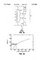
- FIG. 16is a plot of the pump power versus the output power for a specific embodiment of the invention.
- FIG. 17is a schematic representation of an embodiment of the invention in which the long wavelength radiation from a pair of long wavelength VCSELs propagate in a direction opposite to that of the pump radiation;
- FIG. 18is a schematic representation of an embodiment of the invention similar to that illustrated in FIG. 17 except that the long wavelength VCSELs are slightly angled from the short wavelength VCSELs.
- An alternative to electrical injection of charge carriers into the active regionis light injection at a wavelength shorter than the desired emission.
- the injected lightis absorbed in the long wavelength cavity, generating electrons and holes. These charge carriers in turn diffuse into the quantum wells and re-emit at the longer wavelength. Since optical pumping does not require electrical contacts, fabrication is much simpler and resistive heating does not occur.
- the carriersare injected by light, the light can be injected through the mirrors. In electrical pumping schemes the injection must occur around the mirror, assuming that the mirror is electrically insulating.
- the cavitycan be free of dopants, the dopants being a major source of optical loss in VCSELs utilizing electrical injection.
- FIG. 3is a schematic representation of a generic configuration of the present invention.
- FIGS. 4-7, 9-11, and 17-18show two short wavelength VCSELs 43 optically pumping two long wavelength VCSELs 40.
- This configurationis not intended to be limiting, but to indicate schematically the wafer-scale nature of the fabrication technology.
- This same technologycan be used to make single devices consisting of one short wavelength VCSEL pumping one long wavelength VCSEL, or to make large one and two dimensional arrays.
- Lasers 43are a pair of electrically pumped, short wavelength VCSELs. They are comprised of a short wavelength active region 31 interposed between short wavelength mirrors 32. Short wavelength radiation is emitted from a top surface 33 of VCSELs 43 into the bottom surface of a second pair of VCSELs 40.
- VCSELs 40are a pair of long wavelength VCSELs comprised of a long wavelength active region 35 interposed between a bottom mirror 36 and top mirrors 37.
- Mirrors 36 and 37are long wavelength mirrors.
- Mirror 36is transparent to the short wavelength radiation emitted by VCSELs 43.
- Long wavelength radiationis emitted from top mirrors 37. Modulation of the long wavelength radiation is accomplished by modulating the short wavelength pump VCSELs. In an alternate embodiment, modulation is accomplished by applying contacts to the long wavelength VCSELs.
- FIG. 3 and succeeding device schematicsshow the short wavelength VCSEL bottom mirrors 32 and long wavelength VCSEL top mirrors 37 as vertically etched to form cylindrical posts. These posts divide up the initially planar wafer into many refractive index guided devices. Index guiding is well known in the art, and can be accomplished by etching, lateral oxidation, implantation, diffusion, regrowth, or selective growth. In the preferred embodiment, both short wavelength and long wavelength VCSELs should be index guided, although the short wavelength VCSELs could be gain guided or thermally lensed.
- the optically pumped configuration of FIG. 3retains the advantages of VCSELs in general, such as the possibility of wafer-scale fabrication and testing, and inexpensive one and two dimensional array fabrication. This is in marked contrast to VCSELs which used solid-state, dye, or in-plane semiconductor lasers as the optical pump. Optically pumped VCSELs which employ these latter approaches are impractical for array applications and cannot be manufactured or tested on a wafer scale.
- FIG. 4is a schematic representation of one embodiment of the invention.
- Long wavelength VCSELs 40employ a wafer-fused, undoped, GaAs/AlAs mirror 41 on the bottom side, and dielectric mirrors 42 on the top side.
- Dielectric mirrors 42are formed from alternating layers of silicon dioxide, SiO 2 , and titanium dioxide, TiO 2 .
- Dielectric mirrors 42can also be formed using other dielectric materials.
- Long wavelength VCSELs 40are fixed to short wavelength VCSELs 43 by means of a transparent optical adhesive 44 between GaAs substrates 45 and 46.
- FIG. 5is essentially the same embodiment as shown in FIG.
- GaAs substrate 45 of long wavelength VCSELs 40is wafer-fused to GaAs substrate 46 of short wavelength VCSELs 43 at an interface 50.
- This approacheliminates the need for an optical adhesive, possibly leading to a reduction in parasitic reflections.
- GaAs/AlAs mirror 41can be grown in the same epitaxial step as VCSELs 43, thus eliminating the need for either an optical adhesive 44 or wafer fusion 50 at this interface.
- FIG. 7is a schematic representation of an alternate embodiment of the invention.
- Long wavelength VCSELs 40are comprised of a long wavelength active region 60 interposed between two GaAs/AlAs mirrors 61. Active region 60 is wafer-fused to mirrors 61 at interfaces 62.
- the double-fused structureis joined to short wavelength VCSELs 43 with optical adhesive 44.
- the double-fused structurecan also be wafer fused to VCSELs 43 as illustrated in FIG. 5.
- FIG. 8is a schematic representation of an embodiment utilizing integrated microlenses.
- multiple short wavelength VCSELs 43are used to optically pump multiple long wavelength VCSELs 40.
- the arrays of VCSELsare separated by a mechanical spacer 70.
- a set of GaAs microlenses 71which are used to focus the radiation from VCSELs 43 into VCSELs 40.
- Microlenses 71are formed directly in the GaAs substrate 72 of the short wavelength VCSELs (shown), directly in the GaAs substrate of the long wavelength VCSELs (not shown), or both.
- microlenses 71are formed of a material other than GaAs, such as a glass or a reflowable polymer. In this alternate configuration microlenses 71 are not monolithically integrated with the other parts of the device.
- FIG. 9illustrates an alternate technique of attaching long wavelength VCSELs 40 to short wavelength VCSELs 43.
- the two pairs of VCSELsare joined at a metal interface 75 using metal to metal bonding.
- a set of windows 76 in metal interface 75allow the pump radiation to pass through.
- Microlensescan be incorporated into the windows (not shown).
- the bonding metalthe preferred embodiment uses either palladium or indium containing solder.
- FIG. 10is a schematic representation of an embodiment of the invention in which VCSELs 40 utilize dielectric mirrors 80 and 81.
- this embodimentdoes not require the use of the wafer fusion process.
- dielectric mirror 81is joined to VCSELs 43 using a dielectric to semiconductor bond which is known in the art.
- long wavelength active region 60is interposed between dielectric mirror 42 and a bottom mirror 90.
- Mirror 90is formed by epitaxially growing alternating layers of InP and InAlAs. To create the final mirror the structure is etched, exposing the sidewalls of the InAlAs material. The aluminum in the InAlAs is then oxidized in from the sides, creating In w Al x As y O z which has a much lower refractive index than InAlAs or InP. The result is that a low reflectivity mirror is converted to a high reflectivity mirror.
- the lateral oxidation techniquecan also be accomplished with compounds containing aluminum and antimony.
- FIG. 12shows the reflectivity graphs for two particular mirror designs for an embodiment of the invention in which short wavelength VCSELs 43 emit at 980 nanometers and long wavelength VCSELs 40 emit at 1550 nanometers.
- Graph 100is the reflection spectra for a GaAs/AlAs mirror suitable for the bottom mirror of VCSELs 40. This mirror transmits the pump wavelength and reflects the long wavelength of VCSELs 40.
- Graph 101is the reflection spectra for a SiO 2 /TiO 2 dielectric mirror suitable for the top mirrors of VCSELs 40. The dielectric mirror can be designed to either transmit or reflect at VCSEL 43s' wavelength.
- VCSELs 40transmits at this wavelength, as shown in plot 101, then VCSELs 40 only see one pass of the radiation from pump VCSELs 43. If the dielectric reflects at the pump wavelength (not shown), then VCSELs 40 see two passes of the radiation from pump VCSELs 43.
- the dielectric mirrorpartially reflecting it is possible to design a double-pass configuration which increases the absorption and therefore the pumping efficiency. It is also possible to make both the top and bottom mirrors of the long wavelength VCSELs partially reflecting at the pump wavelength, creating resonant pump absorption and an increase in pumping efficiency. This last configuration, however, is difficult to implement.
- FIG. 13is a schematic representation of a specific long wavelength VCSEL suitable for use in this invention.
- Two lattice matched InGaAs quantum wells 110are placed on two peaks of the optical standing wave.
- Quaternary InGaAsP material 111 surrounding these wellsabsorbs the pump radiation and funnels the charge carriers into the wells where they re-emit at 1550 nanometers.
- the absorption coefficient of this materialis on the order of 1.5 ⁇ 10 4 cm - 1, so for the lengths indicated 90 percent of the incident radiation is absorbed in two passes through the cavity.
- FIG. 13also shows that the long wavelength cavity has a larger transverse dimension 112 than the pump transverse dimension 113.
- transverse dimension 112 of the long wavelength VCSELis defined by a lateral refractive index variation (i.e., index guided).
- the index variationcan be defined in any or all of the vertical layers of the device, and can be accomplished by chemical etching, regrowth, implantation, diffusion, disordering, selective growth, or other techniques. Index guiding is well known in the art of semiconductor lasers.
- FIG. 14is a detailed energy band diagram of the preferred absorber design for the embodiment shown in FIG. 13.
- the vertical axis of this diagramrepresents vertical distance in the structure while the horizontal axis represents relative energy.
- Graph 114shows the energy level as a function of vertical distance for the valence band.
- Graph 115shows the energy level as a function of vertical distance for the conduction band.
- absorbing material 111is compositionally graded to create a built-in electric field. The built-in electric field aids in the speed and efficiency with which photogenerated charge carriers are collected in quantum wells 110.
- absorber 111is comprised of compositionally graded InGaAsP 116 and 117.
- Portions 116are graded from 1.15 micrometer bandgap material on the bottom to 1.3 micrometer bandgap material on the top. Portions 117 are graded from 1.3 micrometer bandgap material on the bottom to 1.15 micrometer bandgap material on the top.
- a buffer layer 118 of InPis also shown in this diagram.
- the power at 1550 nanometers versus the power at 980 nanometers, the wavelength of the pump VCSEL in the preferred embodiment,is given by:
- the threshold pump powercan be calculated using the quantum-well gain curve shown in FIG. 15. To reach threshold, the quantum wells must provide a roundtrip gain equal to the roundtrip loss, which is T+A. Since the cavity is free of dopants, the roundtrip absorption/scattering/diffraction losses can be very small, approximately 0.1 percent. Given an output transmission of 0.3 percent, the threshold gain is 0.4 percent.
- the total required current densityis 540 A/cm 2 since there are two quantum wells or, equivalently, the absorbed power density must be 680 W/cm 2 . Assuming 85 percent of the pump radiation is absorbed, 800 W/cm 2 is needed to reach threshold. If this power is uniformly distributed over a 10 micrometer diameter VCSEL, then the total required power is 0.6 mW to reach threshold. Since some of the injected carriers may diffuse laterally outside the optical mode, the number of injected carriers required to reach threshold is higher than this number. Therefore to compensate for the lost carriers, the threshold power is adjusted to 1.0 mW.
- FIG. 16illustrates that for this specific embodiment of the invention, approximately 1 mW of output power can be achieved with a 980 nanometers pump power of 4 mW. By increasing the pump power, improving the absorption efficiency, or using a more advanced gain medium, the output power can be increased. Higher output powers can also be obtained using the configuration illustrated in FIG. 8.
- the power-out versus power-in graph of FIG. 16is shown as linear over a large power range.
- Typical electrically pumped VCSEL curvesshow a rollover at large drive currents due to heating. This effect is not shown in FIG. 16 since heating during optical pumping is far less than during electrical pumping.
- the thermal impedance of the structure shown in FIG. 4is on the order of 1° K. per mW. This means that 1 mW of heat dumped into the cavity will result in a temperature rise of 1° K. In the example discussed above, a 4 mW pump was required to generate 1 mW of long wavelength output.
- the long wavelength radiationpropagates in a direction opposite that of the pump radiation.
- FIG. 17is a schematic representation of one possible configuration of this embodiment.
- short wavelength active region 31is interposed between short wavelength mirrors 85 and 86.
- Mirrors 86reflect essentially 100 percent of the short wavelength emission, but are essentially transparent to the long wavelength emission.
- long wavelength VCSELs 40are slightly angled in relation to short wavelength VCSELs 43. The angling of the two arrays allow the long wavelength radiation to bypass short wavelength mirrors 86.
Landscapes
- Physics & Mathematics (AREA)
- Optics & Photonics (AREA)
- Engineering & Computer Science (AREA)
- Nanotechnology (AREA)
- Chemical & Material Sciences (AREA)
- Condensed Matter Physics & Semiconductors (AREA)
- General Physics & Mathematics (AREA)
- Electromagnetism (AREA)
- Biophysics (AREA)
- Crystallography & Structural Chemistry (AREA)
- Life Sciences & Earth Sciences (AREA)
- Semiconductor Lasers (AREA)
- Lasers (AREA)
Abstract
Description
i P.sub.1.5 =(P.sub.0.98 -P.sub.th)η.sub.i η.sub.conv (T/(T+A)!(1)
η.sub.i =fraction of injected photons recombining radiatively in the wells
η.sub.conv =energy loss from 980 nm to 1550 nm =980/1550=0.63
T=fractional transmission of output mirror at 1550 nm
A=fraction of light lost to absorption/scattering/diffraction per roundtrip
P.sub.th =pump power required to reach threshold.
Claims (22)
Priority Applications (10)
| Application Number | Priority Date | Filing Date | Title |
|---|---|---|---|
| US08/422,486US5513204A (en) | 1995-04-12 | 1995-04-12 | Long wavelength, vertical cavity surface emitting laser with vertically integrated optical pump |
| KR1019960706848AKR100229051B1 (en) | 1995-04-12 | 1996-03-11 | Long wavelength vertical cavity surface emitting laser with vertically integrated optical pump |
| ES96909501TES2152017T3 (en) | 1995-04-12 | 1996-03-11 | VERTICAL CAVITY SURFACE EMISSION LASER, GREAT WAVE LENGTH, WITH VERTICALLY INTEGRATED OPTICAL PUMP. |
| CA002190843ACA2190843C (en) | 1995-04-12 | 1996-03-11 | Long wavelength, vertical cavity surface emitting laser with vertically integrated optical pump |
| PCT/US1996/002323WO1996032766A1 (en) | 1995-04-12 | 1996-03-11 | Long wavelength, vertical cavity surface emitting laser with vertically integrated optical pump |
| JP8530996AJPH10501927A (en) | 1995-04-12 | 1996-03-11 | Long-wavelength vertical cavity surface for laser radiation with vertically integrated optical pump |
| RU97100734/28ARU2153746C2 (en) | 1995-04-12 | 1996-03-11 | Optical device |
| EP96909501AEP0765536B1 (en) | 1995-04-12 | 1996-03-11 | Long wavelength, vertical cavity surface emitting laser with vertically integrated optical pump |
| AU52973/96AAU5297396A (en) | 1995-04-12 | 1996-03-11 | Long wavelength, vertical cavity surface emitting laser with vertically integrated optical pump |
| DE69610598TDE69610598T2 (en) | 1995-04-12 | 1996-03-11 | LONG-WAVE, SURFACE-EMITTING LASER WITH VERTICAL RESONATOR AND INTEGRATED, VERTICAL OPTICAL PUMP SOURCE |
Applications Claiming Priority (1)
| Application Number | Priority Date | Filing Date | Title |
|---|---|---|---|
| US08/422,486US5513204A (en) | 1995-04-12 | 1995-04-12 | Long wavelength, vertical cavity surface emitting laser with vertically integrated optical pump |
Publications (1)
| Publication Number | Publication Date |
|---|---|
| US5513204Atrue US5513204A (en) | 1996-04-30 |
Family
ID=23675104
Family Applications (1)
| Application Number | Title | Priority Date | Filing Date |
|---|---|---|---|
| US08/422,486Expired - LifetimeUS5513204A (en) | 1995-04-12 | 1995-04-12 | Long wavelength, vertical cavity surface emitting laser with vertically integrated optical pump |
Country Status (10)
| Country | Link |
|---|---|
| US (1) | US5513204A (en) |
| EP (1) | EP0765536B1 (en) |
| JP (1) | JPH10501927A (en) |
| KR (1) | KR100229051B1 (en) |
| AU (1) | AU5297396A (en) |
| CA (1) | CA2190843C (en) |
| DE (1) | DE69610598T2 (en) |
| ES (1) | ES2152017T3 (en) |
| RU (1) | RU2153746C2 (en) |
| WO (1) | WO1996032766A1 (en) |
Cited By (88)
| Publication number | Priority date | Publication date | Assignee | Title |
|---|---|---|---|---|
| EP0820128A1 (en)* | 1996-07-17 | 1998-01-21 | Commissariat A L'energie Atomique | Method of assambling two structures and microoptical device obtained by using this method |
| EP0821451A1 (en)* | 1996-07-26 | 1998-01-28 | Commissariat A L'energie Atomique | Solid state microlaser optically pumped by a vertical cavity semiconductor laser |
| WO1998008278A1 (en)* | 1996-08-21 | 1998-02-26 | W.L. Gore & Associates, Inc. | Vertical cavity surface emitting lasers using patterned wafer fusion |
| US5732103A (en)* | 1996-12-09 | 1998-03-24 | Motorola, Inc. | Long wavelength VCSEL |
| US5754578A (en)* | 1996-06-24 | 1998-05-19 | W. L. Gore & Associates, Inc. | 1250-1650 nm vertical cavity surface emitting laser pumped by a 700-1050 nm vertical cavity surface emitting laser |
| WO1998031080A1 (en)* | 1997-01-08 | 1998-07-16 | W.L. Gore & Associates, Inc. | Vcsel-based multi-wavelength transmitter and receiver modules for serial and parallel optical links |
| US5796771A (en)* | 1996-08-19 | 1998-08-18 | The Regents Of The University Of California | Miniature self-pumped monolithically integrated solid state laser |
| WO1998048492A1 (en)* | 1997-04-23 | 1998-10-29 | Honeywell Inc. | Electronic devices formed from pre-patterned structures that are bonded |
| EP0892474A1 (en)* | 1997-07-14 | 1999-01-20 | Mitel Semiconductor AB | Field modulated vertical cavity surface-emitting laser with internal optical pumping |
| EP0881671A3 (en)* | 1997-05-28 | 1999-06-30 | Matsushita Electric Industrial Co., Ltd. | Method for fabricating semiconductor device |
| US5933402A (en)* | 1996-05-15 | 1999-08-03 | Samsung Electronics Co., Ltd. | Optical pickup capable of compatibly adopting disks of different thickness |
| US5977604A (en)* | 1996-03-08 | 1999-11-02 | The Regents Of The University Of California | Buried layer in a semiconductor formed by bonding |
| US6015980A (en)* | 1996-03-08 | 2000-01-18 | The Regents Of The University Of California | Metal layered semiconductor laser |
| US6043515A (en)* | 1996-09-17 | 2000-03-28 | Kabushiki Kaisha Toshiba | Optical semiconductor device |
| GB2342773A (en)* | 1998-10-17 | 2000-04-19 | Mitel Semiconductor Ab | Long wavelength vertical cavity laser with integrated short wavelength pump laser |
| EP0999621A1 (en)* | 1998-11-05 | 2000-05-10 | Gore Enterprise Holdings, Inc. | Semiconductor device with aligned oxide apertures and contact to an intervening layer |
| WO2000062384A1 (en)* | 1999-04-13 | 2000-10-19 | Gore Enterprise Holdings, Inc. | Intra-cavity optically pumped vertical cavity surface emitting laser |
| US6148016A (en)* | 1997-11-06 | 2000-11-14 | The Regents Of The University Of California | Integrated semiconductor lasers and photodetectors |
| WO2001033678A1 (en)* | 1999-10-29 | 2001-05-10 | E20 Communications, Inc. | Method and apparatus for integrated optically pumped vertical cavity surface emitting lasers |
| US6243407B1 (en) | 1997-03-21 | 2001-06-05 | Novalux, Inc. | High power laser devices |
| US6252896B1 (en) | 1999-03-05 | 2001-06-26 | Agilent Technologies, Inc. | Long-Wavelength VCSEL using buried bragg reflectors |
| KR20010107524A (en)* | 2000-05-24 | 2001-12-07 | 이형도 | Two-wavelenght laser diode and method for manufacture thereof |
| US6341137B1 (en) | 1999-04-27 | 2002-01-22 | Gore Enterprise Holdings, Inc. | Wavelength division multiplexed array of long-wavelength vertical cavity lasers |
| US20020094668A1 (en)* | 1998-10-16 | 2002-07-18 | Bernard Aspar | Thin layer structure made up of conductive and insulative zones |
| US6434180B1 (en)* | 2000-12-19 | 2002-08-13 | Lucent Technologies Inc. | Vertical cavity surface emitting laser (VCSEL) |
| US6445724B2 (en)* | 2000-02-23 | 2002-09-03 | Sarnoff Corporation | Master oscillator vertical emission laser |
| WO2002075868A3 (en)* | 2001-03-15 | 2002-12-12 | Ecole Polytech | Vertical cavity surface emitting laser |
| US20030002545A1 (en)* | 2001-07-02 | 2003-01-02 | Wenbin Jiang | Method and apparatus for wavelength tuning of optically pumped vertical cavity surface emitting lasers |
| US6553048B2 (en) | 1999-10-29 | 2003-04-22 | E2O Communications, Inc. | Modulated integrated optically pumped vertical cavity surface emitting lasers |
| US6553051B1 (en) | 2000-10-31 | 2003-04-22 | Agilent Technologies, Inc. | System for optically pumping a long wavelength laser using a short wavelength laser |
| WO2003034559A1 (en)* | 2001-10-19 | 2003-04-24 | Vichel Inc. | Vertically integrated high power surface emitting semiconductor laser device and method of producing the same |
| US6556610B1 (en) | 2001-04-12 | 2003-04-29 | E20 Communications, Inc. | Semiconductor lasers |
| US6567454B1 (en)* | 2001-05-01 | 2003-05-20 | Sandia Corporation | Coupled-resonator vertical-cavity lasers with two active gain regions |
| US20030096439A1 (en)* | 1999-09-20 | 2003-05-22 | Hsing-Chung Lee | Methods for forming index guided vertical cavity surface emitting lasers |
| RU2208268C2 (en)* | 2000-07-14 | 2003-07-10 | Общество с ограниченной ответственностью "ИКО" | Semiconductor infrared radiator |
| US20030156611A1 (en)* | 2002-02-21 | 2003-08-21 | Hoki Kwon | GaAs/Al(Ga)As distributed bragg reflector on InP |
| US20030156610A1 (en)* | 2002-02-21 | 2003-08-21 | Hoki Kwon | Carbon doped GaAsSb suitable for use in tunnel junctions of long-wavelength VCSELs |
| US6647050B2 (en) | 2001-09-18 | 2003-11-11 | Agilent Technologies, Inc. | Flip-chip assembly for optically-pumped lasers |
| US20030219917A1 (en)* | 1998-12-21 | 2003-11-27 | Johnson Ralph H. | System and method using migration enhanced epitaxy for flattening active layers and the mechanical stabilization of quantum wells associated with vertical cavity surface emitting lasers |
| US6671304B2 (en) | 2001-08-28 | 2003-12-30 | The United States Of America As Represented By The Secretary Of The Navy | Amplitude-modulated laser for high-bandwidth communications systems |
| US20040028100A1 (en)* | 2002-08-09 | 2004-02-12 | Hitachi, Ltd. | Optical transmitter equipment and semiconductor laser device |
| US6714574B2 (en) | 2001-07-31 | 2004-03-30 | Bookham Technology, Plc | Monolithically integrated optically-pumped edge-emitting semiconductor laser |
| US6714573B2 (en)* | 2000-08-22 | 2004-03-30 | The Regents Of The University Of California | Contact scheme for intracavity-contacted vertical-cavity surface-emitting laser |
| US20040066826A1 (en)* | 2001-12-13 | 2004-04-08 | Emmanuel Picard | Micro-cavity light emitting device and method for making same |
| US20040069208A1 (en)* | 2000-07-14 | 2004-04-15 | Lommen Franciscus Alphons Marie | Process for crystallizing enantiomerically enriched 2-acetylthio-3-phenylpropionic acid |
| US6746777B1 (en) | 2000-05-31 | 2004-06-08 | Applied Optoelectronics, Inc. | Alternative substrates for epitaxial growth |
| US20040141538A1 (en)* | 2002-09-19 | 2004-07-22 | Osram Opto Semiconductors Gmbh | Optically pumped semiconductor laser apparatus |
| US6798804B2 (en)* | 2000-02-09 | 2004-09-28 | Fuji Photo Film Co., Ltd. | Laser apparatus including surface-emitting semiconductor excited with semiconductor laser element, and directly modulated |
| US20040208216A1 (en)* | 2001-04-11 | 2004-10-21 | Naone Ryan Likeke | Long wavelength vertical cavity surface emitting laser |
| US6810064B1 (en)* | 2000-08-22 | 2004-10-26 | The Regents Of The University Of California | Heat spreading layers for vertical cavity surface emitting lasers |
| US20040217362A1 (en)* | 2001-02-01 | 2004-11-04 | Slater David B | Light emitting diodes including pedestals |
| US20050025211A1 (en)* | 2000-07-12 | 2005-02-03 | Princeton Optronics, Inc. | VCSEL and VCSEL array having integrated microlenses for use in a semiconductor laser pumped solid state laser system |
| WO2005004245A3 (en)* | 2003-06-28 | 2005-06-02 | Univ Heriot Watt | Photoluminescent infrared source |
| US20050129078A1 (en)* | 1998-12-21 | 2005-06-16 | Johnson Ralph H. | Multicomponent barrier layers in quantum well active regions to enhance confinement and speed |
| US20050157765A1 (en)* | 1998-12-21 | 2005-07-21 | Honeywell International Inc. | Low temperature grown layers with migration enhanced epitaxy adjacent to an InGaAsN(Sb) based active region |
| US6922426B2 (en) | 2001-12-20 | 2005-07-26 | Finisar Corporation | Vertical cavity surface emitting laser including indium in the active region |
| US20050169340A1 (en)* | 2004-01-29 | 2005-08-04 | Anikitchev Serguei G. | Optically pumped edge-emitting semiconductor laser |
| FR2870051A1 (en)* | 2004-05-04 | 2005-11-11 | Commissariat Energie Atomique | RADIATION TRANSMITTER WITH INCLINE PUMP BEAM |
| US6975660B2 (en) | 2001-12-27 | 2005-12-13 | Finisar Corporation | Vertical cavity surface emitting laser including indium and antimony in the active region |
| US20060078031A1 (en)* | 2004-10-08 | 2006-04-13 | Govorkov Sergei V | InGaN LED pumped II-VI semiconductor laser |
| US7058112B2 (en) | 2001-12-27 | 2006-06-06 | Finisar Corporation | Indium free vertical cavity surface emitting laser |
| US7095770B2 (en) | 2001-12-20 | 2006-08-22 | Finisar Corporation | Vertical cavity surface emitting laser including indium, antimony and nitrogen in the active region |
| US20060203870A1 (en)* | 2005-02-16 | 2006-09-14 | Samsung Electronics Co., Ltd. | Modulator integrated semiconductor laser device |
| US20060246700A1 (en)* | 1998-12-21 | 2006-11-02 | Johnson Ralph H | Migration enhanced epitaxy fabrication of active regions having quantum wells |
| US7167495B2 (en) | 1998-12-21 | 2007-01-23 | Finisar Corporation | Use of GaAs extended barrier layers between active regions containing nitrogen and AlGaAs confining layers |
| US20070104241A1 (en)* | 2005-11-09 | 2007-05-10 | Samsung Electric Co., Ltd. | Vertical external cavity surface emitting laser with pump beam reflector |
| US20070201525A1 (en)* | 2004-10-01 | 2007-08-30 | Finisar Corporation | Vertical cavity surface emitting laser having strain reduced quantum wells |
| US7266279B1 (en) | 2005-03-25 | 2007-09-04 | Hrl Laboratories, Llc | Optically pumped stepped multi-well laser |
| US20070217474A1 (en)* | 2005-12-20 | 2007-09-20 | Denso Corporation | Laser equipment |
| US20080049802A1 (en)* | 2006-08-25 | 2008-02-28 | Samsung Electronics Co., Ltd | Semiconductor laser diode having wafer-bonded structure and method of fabricating the same |
| US20080151948A1 (en)* | 2006-12-21 | 2008-06-26 | Govorkov Sergei V | Frequency-doubled edge-emitting semiconductor lasers |
| US7408964B2 (en) | 2001-12-20 | 2008-08-05 | Finisar Corporation | Vertical cavity surface emitting laser including indium and nitrogen in the active region |
| WO2009109166A3 (en)* | 2008-03-03 | 2009-11-19 | Osram Opto Semiconductors Gmbh | Surface-emitting semiconductor laser having a monolithic integrated pump laser |
| US20090304039A1 (en)* | 2006-04-13 | 2009-12-10 | Osram Opto Semiconductors Gmbh | Optoelectronic semiconductor element |
| CN1653832B (en)* | 2002-05-08 | 2010-04-28 | 美商威睿电通公司 | Fast traffic channel reconnection system and method |
| US20100177798A1 (en)* | 2009-01-13 | 2010-07-15 | Curtis Robert Menyuk | Passively mode locked quantum cascade lasers |
| US7826511B1 (en)* | 2005-03-25 | 2010-11-02 | Hrl Laboratories, Llc | Optically pumped laser with an integrated optical pump |
| US20110026553A1 (en)* | 2009-07-29 | 2011-02-03 | Forrest Stephen R | Organic laser |
| US20110090930A1 (en)* | 2004-10-01 | 2011-04-21 | Finisar Corporation | Vertical cavity surface emitting laser with undoped top mirror |
| US20120097983A1 (en)* | 2009-05-05 | 2012-04-26 | 3M Innovative Properties Company | Re-emitting semiconductor carrier devices for use with leds and methods of manufacture |
| US20120235191A1 (en)* | 2011-03-18 | 2012-09-20 | Kabushiki Kaisha Toshiba | Semiconductor light emitting device and photocoupler |
| US8687201B2 (en) | 2012-08-31 | 2014-04-01 | Lightlab Imaging, Inc. | Optical coherence tomography control systems and methods |
| US20170125975A1 (en)* | 2015-10-30 | 2017-05-04 | Canon Kabushiki Kaisha | Laser device, information acquisition device, and imaging system |
| JP2017147256A (en)* | 2016-02-15 | 2017-08-24 | 株式会社リコー | Optical amplifier, optical amplifier driving method, and optical amplification method |
| US9755402B2 (en) | 2010-06-28 | 2017-09-05 | Iulian Basarab Petrescu-Prahova | Edge emitter semiconductor laser type of device with end segments for mirrors protection |
| US9912118B2 (en) | 2010-06-28 | 2018-03-06 | Iulian Basarab Petrescu-Prahova | Diode laser type device |
| CN113454859A (en)* | 2019-03-25 | 2021-09-28 | 富士胶片商业创新有限公司 | Light emitting element array chip, light emitting device, optical device, and information processing device |
| CN114142346A (en)* | 2020-09-04 | 2022-03-04 | 浙江睿熙科技有限公司 | Monolithic integrated VCSEL chip |
Families Citing this family (8)
| Publication number | Priority date | Publication date | Assignee | Title |
|---|---|---|---|---|
| US5946121A (en)* | 1996-07-02 | 1999-08-31 | Motorola, Inc. | IrDA data link with VCSEL light source |
| JP4062648B2 (en)* | 1998-12-25 | 2008-03-19 | シャープ株式会社 | Semiconductor laser and manufacturing method thereof |
| JP2003195125A (en)* | 2001-12-27 | 2003-07-09 | Seiko Epson Corp | Optical module and optical communication system |
| US6836495B2 (en)* | 2003-05-07 | 2004-12-28 | Eastman Kodak Company | Vertical cavity laser including inorganic spacer layers |
| US6790696B1 (en)* | 2003-06-30 | 2004-09-14 | Eastman Kodak Company | Providing an organic vertical cavity laser array device with etched region in dielectric stack |
| US8891569B2 (en)* | 2011-03-09 | 2014-11-18 | Koninklijke Philips N.V. | VCSEL array with increased efficiency |
| WO2016195701A1 (en)* | 2015-06-05 | 2016-12-08 | Iulian Basarab Petrescu-Prahova | Emitter semiconductor laser type of device |
| JP7663620B2 (en) | 2023-03-28 | 2025-04-16 | キヤノン株式会社 | Light emitting device, distance measuring device and moving object |
Citations (14)
| Publication number | Priority date | Publication date | Assignee | Title |
|---|---|---|---|---|
| JPS63280484A (en)* | 1987-05-12 | 1988-11-17 | Matsushita Electric Ind Co Ltd | Semiconductor device |
| US4873696A (en)* | 1988-10-31 | 1989-10-10 | The Regents Of The University Of California | Surface-emitting lasers with periodic gain and a parallel driven nipi structure |
| US4906839A (en)* | 1986-05-01 | 1990-03-06 | Pencom International Corp. | Hybrid surface emitting laser and detector |
| US5115441A (en)* | 1991-01-03 | 1992-05-19 | At&T Bell Laboratories | Vertical cavity surface emmitting lasers with transparent electrodes |
| US5115442A (en)* | 1990-04-13 | 1992-05-19 | At&T Bell Laboratories | Top-emitting surface emitting laser structures |
| US5170407A (en)* | 1991-10-11 | 1992-12-08 | At&T Bell Laboratories | Elimination of heterojunction band discontinuities |
| US5206872A (en)* | 1991-11-01 | 1993-04-27 | At&T Bell Laboratories | Surface emitting laser |
| US5212706A (en)* | 1991-12-03 | 1993-05-18 | University Of Connecticut | Laser diode assembly with tunnel junctions and providing multiple beams |
| US5212703A (en)* | 1992-02-18 | 1993-05-18 | Eastman Kodak Company | Surface emitting lasers with low resistance bragg reflectors |
| JPH05145173A (en)* | 1991-11-21 | 1993-06-11 | Fuji Electric Co Ltd | Semiconductor laser device |
| US5341390A (en)* | 1992-04-16 | 1994-08-23 | Hewlett-Packard Company | Surface emitting second harmonic generating device |
| US5343487A (en)* | 1992-10-01 | 1994-08-30 | Optical Concepts, Inc. | Electrical pumping scheme for vertical-cavity surface-emitting lasers |
| US5345456A (en)* | 1993-03-11 | 1994-09-06 | National Research Council Of Canada | Spatially addressable surface emission sum frequency device |
| US5363390A (en)* | 1993-11-22 | 1994-11-08 | Hewlett-Packard Company | Semiconductor laser that generates second harmonic light by means of a nonlinear crystal in the laser cavity |
Family Cites Families (2)
| Publication number | Priority date | Publication date | Assignee | Title |
|---|---|---|---|---|
| US5115445A (en)* | 1988-02-02 | 1992-05-19 | Massachusetts Institute Of Technology | Microchip laser array |
| US5052016A (en)* | 1990-05-18 | 1991-09-24 | University Of New Mexico | Resonant-periodic-gain distributed-feedback surface-emitting semiconductor laser |
- 1995
- 1995-04-12USUS08/422,486patent/US5513204A/ennot_activeExpired - Lifetime
- 1996
- 1996-03-11ESES96909501Tpatent/ES2152017T3/ennot_activeExpired - Lifetime
- 1996-03-11DEDE69610598Tpatent/DE69610598T2/ennot_activeExpired - Fee Related
- 1996-03-11CACA002190843Apatent/CA2190843C/ennot_activeExpired - Fee Related
- 1996-03-11KRKR1019960706848Apatent/KR100229051B1/ennot_activeExpired - Fee Related
- 1996-03-11AUAU52973/96Apatent/AU5297396A/ennot_activeAbandoned
- 1996-03-11WOPCT/US1996/002323patent/WO1996032766A1/enactiveIP Right Grant
- 1996-03-11JPJP8530996Apatent/JPH10501927A/ennot_activeCeased
- 1996-03-11EPEP96909501Apatent/EP0765536B1/ennot_activeExpired - Lifetime
- 1996-03-11RURU97100734/28Apatent/RU2153746C2/ennot_activeIP Right Cessation
Patent Citations (14)
| Publication number | Priority date | Publication date | Assignee | Title |
|---|---|---|---|---|
| US4906839A (en)* | 1986-05-01 | 1990-03-06 | Pencom International Corp. | Hybrid surface emitting laser and detector |
| JPS63280484A (en)* | 1987-05-12 | 1988-11-17 | Matsushita Electric Ind Co Ltd | Semiconductor device |
| US4873696A (en)* | 1988-10-31 | 1989-10-10 | The Regents Of The University Of California | Surface-emitting lasers with periodic gain and a parallel driven nipi structure |
| US5115442A (en)* | 1990-04-13 | 1992-05-19 | At&T Bell Laboratories | Top-emitting surface emitting laser structures |
| US5115441A (en)* | 1991-01-03 | 1992-05-19 | At&T Bell Laboratories | Vertical cavity surface emmitting lasers with transparent electrodes |
| US5170407A (en)* | 1991-10-11 | 1992-12-08 | At&T Bell Laboratories | Elimination of heterojunction band discontinuities |
| US5206872A (en)* | 1991-11-01 | 1993-04-27 | At&T Bell Laboratories | Surface emitting laser |
| JPH05145173A (en)* | 1991-11-21 | 1993-06-11 | Fuji Electric Co Ltd | Semiconductor laser device |
| US5212706A (en)* | 1991-12-03 | 1993-05-18 | University Of Connecticut | Laser diode assembly with tunnel junctions and providing multiple beams |
| US5212703A (en)* | 1992-02-18 | 1993-05-18 | Eastman Kodak Company | Surface emitting lasers with low resistance bragg reflectors |
| US5341390A (en)* | 1992-04-16 | 1994-08-23 | Hewlett-Packard Company | Surface emitting second harmonic generating device |
| US5343487A (en)* | 1992-10-01 | 1994-08-30 | Optical Concepts, Inc. | Electrical pumping scheme for vertical-cavity surface-emitting lasers |
| US5345456A (en)* | 1993-03-11 | 1994-09-06 | National Research Council Of Canada | Spatially addressable surface emission sum frequency device |
| US5363390A (en)* | 1993-11-22 | 1994-11-08 | Hewlett-Packard Company | Semiconductor laser that generates second harmonic light by means of a nonlinear crystal in the laser cavity |
Non-Patent Citations (32)
| Title |
|---|
| C. L. Chua et al. "Dielectrically-Bonded Long Wavelength Vertical Cavity Laser on GaAs Substrates Using Strain-Compensated Multiple Quantum Wells" (Dec. 1994) 6(12) IEEE Photonics Technology Letters, 1400-1402. |
| C. L. Chua et al. Dielectrically Bonded Long Wavelength Vertical Cavity Laser on GaAs Substrates Using Strain Compensated Multiple Quantum Wells (Dec. 1994) 6(12) IEEE Photonics Technology Letters, 1400 1402.* |
| D. I. Babic et al. "Double-Fused 1.52-μVertical-Cavity Lasers" (Oct. 31-Nov. 3 1994) LEOS '94 Conference Proceedings 1, IEEE Lasers and Electro-Optics Society 7th Annual Meeting. |
| D. I. Babic et al. Double Fused 1.52 Vertical Cavity Lasers (Oct. 31 Nov. 3 1994) LEOS 94 Conference Proceedings 1, IEEE Lasers and Electro Optics Society 7th Annual Meeting.* |
| Dubravko Babic et al. "Double-Fused 1.52 μVertical-Cavity Lasers" (Feb. 27 1995) 66(9) Appl. Phys. Lett., 1030-1032. |
| Dubravko Babic et al. Double Fused 1.52 Vertical Cavity Lasers (Feb. 27 1995) 66(9) Appl. Phys. Lett., 1030 1032.* |
| J. J. Dudley et al. "Low Threshold, Wafer Fused Long Wavelength Vertical Cavity Lasers" (Mar. 21 1994) 64(12) Appl. Phys. Lett., 1463-1465. |
| J. J. Dudley et al. Low Threshold, Wafer Fused Long Wavelength Vertical Cavity Lasers (Mar. 21 1994) 64(12) Appl. Phys. Lett., 1463 1465.* |
| James J.Dudley "Wafer Fused Vertical Cavity Lasers" (Aug. 1994) ECE Technical Report #94-21 (especially Chapter 4). |
| James J.Dudley Wafer Fused Vertical Cavity Lasers (Aug. 1994) ECE Technical Report 94 21 (especially Chapter 4).* |
| Lin et al., "Photopumped Long Wavelength Vertical-Cavity Surface-Emitting Lasers Using Strain-Compensated Multiple Quantum Wells" (Jun. 20 1994) 64(25) Appl. Phys. Lett., 3395-3397. |
| Lin et al., Photopumped Long Wavelength Vertical Cavity Surface Emitting Lasers Using Strain Compensated Multiple Quantum Wells (Jun. 20 1994) 64(25) Appl. Phys. Lett., 3395 3397.* |
| McDaniel et al., "Vertical Cavity Surface-Emitting Semiconductor Laser with CW Injection Laser Pumping" (Mar. 1990) 2(3) IEEE Photonics Tech. Lett., 156-158. |
| McDaniel et al., Vertical Cavity Surface Emitting Semiconductor Laser with CW Injection Laser Pumping (Mar. 1990) 2(3) IEEE Photonics Tech. Lett., 156 158.* |
| Optical Concepts, Inc. "A Wavelength Division Multiplexed Fiber-Optic Digital Communication System for Long Haul Parallel High Speed (32 Gb/sec) Communication over a Single Fiber Optic Cable" (Aug. 28 1994) Quarterly Technical Progress Report No. 2 Contract No. DASG60-94-C-0022. |
| Optical Concepts, Inc. "A Wavelength Division Multiplexed Fiber-Optic Digital Communication System for Long Haul Parallel High Speed (32 Gb/sec) Communication over a Single Fiber Optic Cable" (Dec. 23 1994) Quarterly Technical Progress Report No. 3 Contract No. DASG60-94-C-0022. |
| Optical Concepts, Inc. "A Wavelength Division Multiplexed Fiber-Optic Digital Communication System for Long Haul Parallel High Speed (32 Gb/sec) Communication over a Single Fiber Optic Cable" (Mar. 24 1995) Quarterly Technical Progress Report No. 4 Contract No. DASG60-94-C-0022. |
| Optical Concepts, Inc. "Continuous-Wave, Single-Mode, VCSEL Arrays at 1300/1550 nm and Longer Wavelengths, Using Vertically Integrated 980 nm VCSEL Optical Pump" (Jan. 12 1995) U.S. Department of Defense Proposal AF95-106. |
| Optical Concepts, Inc. "Continuous-Wave, Single-Mode, VCSEL Arrays at 1300/1550 nm and Longer wavelengths, Using Vertically Integrated 980 nm VCSEL Optical Pump" (Jan. 12 1995) U.S. Department of Defense Proposal AF95-135. |
| Optical Concepts, Inc. "Long-Wavelength Vertical Cavity Surface-Emitting Lasers with Vertically Integrated Optical Pump" (Dec. 19 1994) White Paper. |
| Optical Concepts, Inc. "Multi-Wavelength WDM Source Using Long-Wavelength Vertical Cavity Laser Array with Vertically Integrated Optical Pump" (Jul. 13, 1994) U.S. Department of Defense Proposal ARPA 94-102. |
| Optical Concepts, Inc. "Vertical-Cavity Lasers for Sub-Carrier Multiplexed 1.55 μWDM Systems for Distributed Computing" (Oct. 15 1994) Final Report Contract No. DASG60-94-C-0039. |
| Optical Concepts, Inc. A Wavelength Division Multiplexed Fiber Optic Digital Communication System for Long Haul Parallel High Speed (32 Gb/sec) Communication over a Single Fiber Optic Cable (Aug. 28 1994) Quarterly Technical Progress Report No. 2 Contract No. DASG60 94 C 0022.* |
| Optical Concepts, Inc. A Wavelength Division Multiplexed Fiber Optic Digital Communication System for Long Haul Parallel High Speed (32 Gb/sec) Communication over a Single Fiber Optic Cable (Dec. 23 1994) Quarterly Technical Progress Report No. 3 Contract No. DASG60 94 C 0022.* |
| Optical Concepts, Inc. A Wavelength Division Multiplexed Fiber Optic Digital Communication System for Long Haul Parallel High Speed (32 Gb/sec) Communication over a Single Fiber Optic Cable (Mar. 24 1995) Quarterly Technical Progress Report No. 4 Contract No. DASG60 94 C 0022.* |
| Optical Concepts, Inc. Continuous Wave, Single Mode, VCSEL Arrays at 1300/1550 nm and Longer Wavelengths, Using Vertically Integrated 980 nm VCSEL Optical Pump (Jan. 12 1995) U.S. Department of Defense Proposal AF95 106.* |
| Optical Concepts, Inc. Continuous Wave, Single Mode, VCSEL Arrays at 1300/1550 nm and Longer wavelengths, Using Vertically Integrated 980 nm VCSEL Optical Pump (Jan. 12 1995) U.S. Department of Defense Proposal AF95 135.* |
| Optical Concepts, Inc. Long Wavelength Vertical Cavity Surface Emitting Lasers with Vertically Integrated Optical Pump (Dec. 19 1994) White Paper.* |
| Optical Concepts, Inc. Multi Wavelength WDM Source Using Long Wavelength Vertical Cavity Laser Array with Vertically Integrated Optical Pump (Jul. 13, 1994) U.S. Department of Defense Proposal ARPA 94 102.* |
| Optical Concepts, Inc. Vertical Cavity Lasers for Sub Carrier Multiplexed 1.55 WDM Systems for Distributed Computing (Oct. 15 1994) Final Report Contract No. DASG60 94 C 0039.* |
| T. Baba et al. "Near Room Temperature Continuous Wave Lasing Characteristics of GaInAsP/InP Surface Emitting Laser" (May 13 1993) 29(10) Electronic Letters, 913-914. |
| T. Baba et al. Near Room Temperature Continuous Wave Lasing Characteristics of GaInAsP/InP Surface Emitting Laser (May 13 1993) 29(10) Electronic Letters, 913 914.* |
Cited By (154)
| Publication number | Priority date | Publication date | Assignee | Title |
|---|---|---|---|---|
| US6208007B1 (en) | 1996-03-08 | 2001-03-27 | The Regents Of The University Of California | Buried layer in a semiconductor formed by bonding |
| US6015980A (en)* | 1996-03-08 | 2000-01-18 | The Regents Of The University Of California | Metal layered semiconductor laser |
| US5977604A (en)* | 1996-03-08 | 1999-11-02 | The Regents Of The University Of California | Buried layer in a semiconductor formed by bonding |
| DE19720416C2 (en)* | 1996-05-15 | 2002-11-07 | Samsung Electronics Co Ltd | Optical sensor that can hold disks of different thicknesses |
| US5933402A (en)* | 1996-05-15 | 1999-08-03 | Samsung Electronics Co., Ltd. | Optical pickup capable of compatibly adopting disks of different thickness |
| US5754578A (en)* | 1996-06-24 | 1998-05-19 | W. L. Gore & Associates, Inc. | 1250-1650 nm vertical cavity surface emitting laser pumped by a 700-1050 nm vertical cavity surface emitting laser |
| EP0820128A1 (en)* | 1996-07-17 | 1998-01-21 | Commissariat A L'energie Atomique | Method of assambling two structures and microoptical device obtained by using this method |
| FR2751467A1 (en)* | 1996-07-17 | 1998-01-23 | Commissariat Energie Atomique | METHOD FOR ASSEMBLING TWO STRUCTURES AND DEVICE OBTAINED BY THE PROCESS. APPLICATIONS TO MICROLASERS |
| US5982802A (en)* | 1996-07-26 | 1999-11-09 | Commissariat A L'energie Atomique | Solid microlaser with optical pumping by vertical cavity semiconductor laser |
| EP0821451A1 (en)* | 1996-07-26 | 1998-01-28 | Commissariat A L'energie Atomique | Solid state microlaser optically pumped by a vertical cavity semiconductor laser |
| FR2751796A1 (en)* | 1996-07-26 | 1998-01-30 | Commissariat Energie Atomique | SOILDE MICROLASER, OPTICALLY PUMPED BY VERTICAL CAVITY SEMICONDUCTOR LASER |
| US5796771A (en)* | 1996-08-19 | 1998-08-18 | The Regents Of The University Of California | Miniature self-pumped monolithically integrated solid state laser |
| US5985686A (en)* | 1996-08-21 | 1999-11-16 | W. L. Gore & Associates, Inc. | Process for manufacturing vertical cavity surface emitting lasers using patterned wafer fusion and the device manufactured by the process |
| WO1998008278A1 (en)* | 1996-08-21 | 1998-02-26 | W.L. Gore & Associates, Inc. | Vertical cavity surface emitting lasers using patterned wafer fusion |
| US6043515A (en)* | 1996-09-17 | 2000-03-28 | Kabushiki Kaisha Toshiba | Optical semiconductor device |
| US5732103A (en)* | 1996-12-09 | 1998-03-24 | Motorola, Inc. | Long wavelength VCSEL |
| US5914976A (en)* | 1997-01-08 | 1999-06-22 | W. L. Gore & Associates, Inc. | VCSEL-based multi-wavelength transmitter and receiver modules for serial and parallel optical links |
| WO1998031080A1 (en)* | 1997-01-08 | 1998-07-16 | W.L. Gore & Associates, Inc. | Vcsel-based multi-wavelength transmitter and receiver modules for serial and parallel optical links |
| US6243407B1 (en) | 1997-03-21 | 2001-06-05 | Novalux, Inc. | High power laser devices |
| WO1998048492A1 (en)* | 1997-04-23 | 1998-10-29 | Honeywell Inc. | Electronic devices formed from pre-patterned structures that are bonded |
| EP0881671A3 (en)* | 1997-05-28 | 1999-06-30 | Matsushita Electric Industrial Co., Ltd. | Method for fabricating semiconductor device |
| US6423561B1 (en) | 1997-05-28 | 2002-07-23 | Matsushita Electric Industrial Co., Ltd. | Method for fabricating semiconductor device |
| US6184066B1 (en) | 1997-05-28 | 2001-02-06 | Matsushita Electric Industrial Co., Ltd. | Method for fabricating semiconductor device |
| US6285704B1 (en) | 1997-07-14 | 2001-09-04 | Mitel Semiconductor Ab | Field modulated vertical cavity surface-emitting laser with internal optical pumping |
| EP0892474A1 (en)* | 1997-07-14 | 1999-01-20 | Mitel Semiconductor AB | Field modulated vertical cavity surface-emitting laser with internal optical pumping |
| US6148016A (en)* | 1997-11-06 | 2000-11-14 | The Regents Of The University Of California | Integrated semiconductor lasers and photodetectors |
| US20020094668A1 (en)* | 1998-10-16 | 2002-07-18 | Bernard Aspar | Thin layer structure made up of conductive and insulative zones |
| GB2342773A (en)* | 1998-10-17 | 2000-04-19 | Mitel Semiconductor Ab | Long wavelength vertical cavity laser with integrated short wavelength pump laser |
| US6372533B2 (en)* | 1998-11-05 | 2002-04-16 | Gore Enterprise Holdings, Inc. | Method of making a semiconductor device with aligned oxide apertures and contact to an intervening layer |
| EP0999621A1 (en)* | 1998-11-05 | 2000-05-10 | Gore Enterprise Holdings, Inc. | Semiconductor device with aligned oxide apertures and contact to an intervening layer |
| US6314118B1 (en) | 1998-11-05 | 2001-11-06 | Gore Enterprise Holdings, Inc. | Semiconductor device with aligned oxide apertures and contact to an intervening layer |
| US7257143B2 (en) | 1998-12-21 | 2007-08-14 | Finisar Corporation | Multicomponent barrier layers in quantum well active regions to enhance confinement and speed |
| US20050157765A1 (en)* | 1998-12-21 | 2005-07-21 | Honeywell International Inc. | Low temperature grown layers with migration enhanced epitaxy adjacent to an InGaAsN(Sb) based active region |
| US20030219917A1 (en)* | 1998-12-21 | 2003-11-27 | Johnson Ralph H. | System and method using migration enhanced epitaxy for flattening active layers and the mechanical stabilization of quantum wells associated with vertical cavity surface emitting lasers |
| US20050142683A1 (en)* | 1998-12-21 | 2005-06-30 | Honeywell International | System for developing a nitrogen-containing active region |
| US7286585B2 (en) | 1998-12-21 | 2007-10-23 | Finisar Corporation | Low temperature grown layers with migration enhanced epitaxy adjacent to an InGaAsN(Sb) based active region |
| US20050129078A1 (en)* | 1998-12-21 | 2005-06-16 | Johnson Ralph H. | Multicomponent barrier layers in quantum well active regions to enhance confinement and speed |
| US7435660B2 (en) | 1998-12-21 | 2008-10-14 | Finisar Corporation | Migration enhanced epitaxy fabrication of active regions having quantum wells |
| US20050034661A1 (en)* | 1998-12-21 | 2005-02-17 | Finisar Corporation | System for developing a nitrogen-containing active region |
| US7378680B2 (en) | 1998-12-21 | 2008-05-27 | Finisar Corporation | Migration enhanced epitaxy fabrication of quantum wells |
| US7167495B2 (en) | 1998-12-21 | 2007-01-23 | Finisar Corporation | Use of GaAs extended barrier layers between active regions containing nitrogen and AlGaAs confining layers |
| US20060246700A1 (en)* | 1998-12-21 | 2006-11-02 | Johnson Ralph H | Migration enhanced epitaxy fabrication of active regions having quantum wells |
| US6252896B1 (en) | 1999-03-05 | 2001-06-26 | Agilent Technologies, Inc. | Long-Wavelength VCSEL using buried bragg reflectors |
| WO2000062384A1 (en)* | 1999-04-13 | 2000-10-19 | Gore Enterprise Holdings, Inc. | Intra-cavity optically pumped vertical cavity surface emitting laser |
| US6341137B1 (en) | 1999-04-27 | 2002-01-22 | Gore Enterprise Holdings, Inc. | Wavelength division multiplexed array of long-wavelength vertical cavity lasers |
| US6822993B2 (en) | 1999-09-20 | 2004-11-23 | Jds Uniphase Corporation | Index guided vertical cavity surface emitting lasers |
| US20030096439A1 (en)* | 1999-09-20 | 2003-05-22 | Hsing-Chung Lee | Methods for forming index guided vertical cavity surface emitting lasers |
| US6577658B1 (en)* | 1999-09-20 | 2003-06-10 | E20 Corporation, Inc. | Method and apparatus for planar index guided vertical cavity surface emitting lasers |
| US6852558B2 (en) | 1999-09-20 | 2005-02-08 | Jds Uniphase Corporation | Methods for forming index guided vertical cavity surface emitting lasers |
| US6940885B1 (en) | 1999-10-29 | 2005-09-06 | Jds Uniphase Corporation | Systems, methods, and apparatuses for optically pumped vertical cavity surface emitting laser devices |
| US6553048B2 (en) | 1999-10-29 | 2003-04-22 | E2O Communications, Inc. | Modulated integrated optically pumped vertical cavity surface emitting lasers |
| US6580741B2 (en)* | 1999-10-29 | 2003-06-17 | E2O Communications, Inc. | Systems with integrated optically pumped vertical cavity surface emitting lasers |
| US20030007538A1 (en)* | 1999-10-29 | 2003-01-09 | Wenbin Jiang | Systems with integrated optically pumped vertical cavity surface emitting lasers |
| WO2001033678A1 (en)* | 1999-10-29 | 2001-05-10 | E20 Communications, Inc. | Method and apparatus for integrated optically pumped vertical cavity surface emitting lasers |
| US6424669B1 (en) | 1999-10-29 | 2002-07-23 | E20 Communications, Inc. | Integrated optically pumped vertical cavity surface emitting laser |
| US6339607B1 (en)* | 1999-10-29 | 2002-01-15 | E2O Communications, Inc. | Method and apparatus for modulated integrated optically pumped vertical cavity surface emitting lasers |
| US6798804B2 (en)* | 2000-02-09 | 2004-09-28 | Fuji Photo Film Co., Ltd. | Laser apparatus including surface-emitting semiconductor excited with semiconductor laser element, and directly modulated |
| US6445724B2 (en)* | 2000-02-23 | 2002-09-03 | Sarnoff Corporation | Master oscillator vertical emission laser |
| KR20010107524A (en)* | 2000-05-24 | 2001-12-07 | 이형도 | Two-wavelenght laser diode and method for manufacture thereof |
| US6746777B1 (en) | 2000-05-31 | 2004-06-08 | Applied Optoelectronics, Inc. | Alternative substrates for epitaxial growth |
| US6888871B1 (en) | 2000-07-12 | 2005-05-03 | Princeton Optronics, Inc. | VCSEL and VCSEL array having integrated microlenses for use in a semiconductor laser pumped solid state laser system |
| US20050025211A1 (en)* | 2000-07-12 | 2005-02-03 | Princeton Optronics, Inc. | VCSEL and VCSEL array having integrated microlenses for use in a semiconductor laser pumped solid state laser system |
| US20040069208A1 (en)* | 2000-07-14 | 2004-04-15 | Lommen Franciscus Alphons Marie | Process for crystallizing enantiomerically enriched 2-acetylthio-3-phenylpropionic acid |
| RU2208268C2 (en)* | 2000-07-14 | 2003-07-10 | Общество с ограниченной ответственностью "ИКО" | Semiconductor infrared radiator |
| US6714573B2 (en)* | 2000-08-22 | 2004-03-30 | The Regents Of The University Of California | Contact scheme for intracavity-contacted vertical-cavity surface-emitting laser |
| US6798817B2 (en)* | 2000-08-22 | 2004-09-28 | The Regents Of The University Of California | Distributed bragg reflectors incorporating SB material for long-wavelength vertical cavity surface emitting lasers |
| US6810064B1 (en)* | 2000-08-22 | 2004-10-26 | The Regents Of The University Of California | Heat spreading layers for vertical cavity surface emitting lasers |
| US6553051B1 (en) | 2000-10-31 | 2003-04-22 | Agilent Technologies, Inc. | System for optically pumping a long wavelength laser using a short wavelength laser |
| US6434180B1 (en)* | 2000-12-19 | 2002-08-13 | Lucent Technologies Inc. | Vertical cavity surface emitting laser (VCSEL) |
| US20040217362A1 (en)* | 2001-02-01 | 2004-11-04 | Slater David B | Light emitting diodes including pedestals |
| US20070284604A1 (en)* | 2001-02-01 | 2007-12-13 | Cree, Inc. | Light emitting diodes including transparent oxide layers |
| US8692277B2 (en) | 2001-02-01 | 2014-04-08 | Cree, Inc. | Light emitting diodes including optically matched substrates |
| US20060131599A1 (en)* | 2001-02-01 | 2006-06-22 | Cree, Inc. | Light emitting diodes including pedestals |
| US8426881B2 (en) | 2001-02-01 | 2013-04-23 | Cree, Inc. | Light emitting diodes including two reflector layers |
| US20090166658A1 (en)* | 2001-02-01 | 2009-07-02 | Cree, Inc. | Light emitting diodes including two reflector layers |
| US7026659B2 (en)* | 2001-02-01 | 2006-04-11 | Cree, Inc. | Light emitting diodes including pedestals |
| US7420222B2 (en) | 2001-02-01 | 2008-09-02 | Cree, Inc. | Light emitting diodes including transparent oxide layers |
| WO2002075868A3 (en)* | 2001-03-15 | 2002-12-12 | Ecole Polytech | Vertical cavity surface emitting laser |
| US6898215B2 (en)* | 2001-04-11 | 2005-05-24 | Optical Communication Products, Inc. | Long wavelength vertical cavity surface emitting laser |
| US7020172B2 (en) | 2001-04-11 | 2006-03-28 | Optical Communication Products, Inc. | Long wavelength vertical cavity surface emitting laser |
| US20040208216A1 (en)* | 2001-04-11 | 2004-10-21 | Naone Ryan Likeke | Long wavelength vertical cavity surface emitting laser |
| US6556610B1 (en) | 2001-04-12 | 2003-04-29 | E20 Communications, Inc. | Semiconductor lasers |
| US6567454B1 (en)* | 2001-05-01 | 2003-05-20 | Sandia Corporation | Coupled-resonator vertical-cavity lasers with two active gain regions |
| US20030002545A1 (en)* | 2001-07-02 | 2003-01-02 | Wenbin Jiang | Method and apparatus for wavelength tuning of optically pumped vertical cavity surface emitting lasers |
| US6717964B2 (en)* | 2001-07-02 | 2004-04-06 | E20 Communications, Inc. | Method and apparatus for wavelength tuning of optically pumped vertical cavity surface emitting lasers |
| US6714574B2 (en) | 2001-07-31 | 2004-03-30 | Bookham Technology, Plc | Monolithically integrated optically-pumped edge-emitting semiconductor laser |
| US6671304B2 (en) | 2001-08-28 | 2003-12-30 | The United States Of America As Represented By The Secretary Of The Navy | Amplitude-modulated laser for high-bandwidth communications systems |
| US6647050B2 (en) | 2001-09-18 | 2003-11-11 | Agilent Technologies, Inc. | Flip-chip assembly for optically-pumped lasers |
| WO2003034559A1 (en)* | 2001-10-19 | 2003-04-24 | Vichel Inc. | Vertically integrated high power surface emitting semiconductor laser device and method of producing the same |
| US20040066826A1 (en)* | 2001-12-13 | 2004-04-08 | Emmanuel Picard | Micro-cavity light emitting device and method for making same |
| US7154929B2 (en)* | 2001-12-13 | 2006-12-26 | Commissariat A L'energie Atomique | Micro-cavity light emitting device and method for making same |
| US7408964B2 (en) | 2001-12-20 | 2008-08-05 | Finisar Corporation | Vertical cavity surface emitting laser including indium and nitrogen in the active region |
| US7095770B2 (en) | 2001-12-20 | 2006-08-22 | Finisar Corporation | Vertical cavity surface emitting laser including indium, antimony and nitrogen in the active region |
| US6922426B2 (en) | 2001-12-20 | 2005-07-26 | Finisar Corporation | Vertical cavity surface emitting laser including indium in the active region |
| US6975660B2 (en) | 2001-12-27 | 2005-12-13 | Finisar Corporation | Vertical cavity surface emitting laser including indium and antimony in the active region |
| US7058112B2 (en) | 2001-12-27 | 2006-06-06 | Finisar Corporation | Indium free vertical cavity surface emitting laser |
| US20030156611A1 (en)* | 2002-02-21 | 2003-08-21 | Hoki Kwon | GaAs/Al(Ga)As distributed bragg reflector on InP |
| US6822995B2 (en) | 2002-02-21 | 2004-11-23 | Finisar Corporation | GaAs/AI(Ga)As distributed bragg reflector on InP |
| US7295586B2 (en) | 2002-02-21 | 2007-11-13 | Finisar Corporation | Carbon doped GaAsSb suitable for use in tunnel junctions of long-wavelength VCSELs |
| US20030156610A1 (en)* | 2002-02-21 | 2003-08-21 | Hoki Kwon | Carbon doped GaAsSb suitable for use in tunnel junctions of long-wavelength VCSELs |
| CN1653832B (en)* | 2002-05-08 | 2010-04-28 | 美商威睿电通公司 | Fast traffic channel reconnection system and method |
| US20040028100A1 (en)* | 2002-08-09 | 2004-02-12 | Hitachi, Ltd. | Optical transmitter equipment and semiconductor laser device |
| US6931039B2 (en)* | 2002-08-09 | 2005-08-16 | Hitachi, Ltd. | Optical transmitter equipment and semiconductor laser device |
| US20040141538A1 (en)* | 2002-09-19 | 2004-07-22 | Osram Opto Semiconductors Gmbh | Optically pumped semiconductor laser apparatus |
| US7224710B2 (en)* | 2002-09-19 | 2007-05-29 | Osram Gmbh | Optically pumped semiconductor laser apparatus |
| WO2005004245A3 (en)* | 2003-06-28 | 2005-06-02 | Univ Heriot Watt | Photoluminescent infrared source |
| US6947466B2 (en) | 2004-01-29 | 2005-09-20 | Coherent, Inc. | Optically pumped edge-emitting semiconductor laser |
| US20050169340A1 (en)* | 2004-01-29 | 2005-08-04 | Anikitchev Serguei G. | Optically pumped edge-emitting semiconductor laser |
| US7300809B2 (en) | 2004-01-29 | 2007-11-27 | Coherent, Inc. | Optically pumped edge-emitting semiconductor laser |
| US20050277215A1 (en)* | 2004-01-29 | 2005-12-15 | Anikitchev Serguei G | Optically pumped edge-emitting semiconductor laser |
| WO2005109584A3 (en)* | 2004-05-04 | 2006-06-29 | Commissariat Energie Atomique | Inclined pump beam radiation emitter |
| US20080031300A1 (en)* | 2004-05-04 | 2008-02-07 | Commissariat A L'energie Atomique | Inclined Pump Beam Radiation Emitter |
| FR2870051A1 (en)* | 2004-05-04 | 2005-11-11 | Commissariat Energie Atomique | RADIATION TRANSMITTER WITH INCLINE PUMP BEAM |
| US8451875B2 (en) | 2004-10-01 | 2013-05-28 | Finisar Corporation | Vertical cavity surface emitting laser having strain reduced quantum wells |
| US20070201525A1 (en)* | 2004-10-01 | 2007-08-30 | Finisar Corporation | Vertical cavity surface emitting laser having strain reduced quantum wells |
| US8168456B2 (en) | 2004-10-01 | 2012-05-01 | Finisar Corporation | Vertical cavity surface emitting laser with undoped top mirror |
| US20110090930A1 (en)* | 2004-10-01 | 2011-04-21 | Finisar Corporation | Vertical cavity surface emitting laser with undoped top mirror |
| WO2006041619A3 (en)* | 2004-10-08 | 2006-07-27 | Coherent Inc | InGaN LED PUMPED II-VI SEMICONDUCTOR LASER |
| US20060078031A1 (en)* | 2004-10-08 | 2006-04-13 | Govorkov Sergei V | InGaN LED pumped II-VI semiconductor laser |
| US20060203870A1 (en)* | 2005-02-16 | 2006-09-14 | Samsung Electronics Co., Ltd. | Modulator integrated semiconductor laser device |
| US7826511B1 (en)* | 2005-03-25 | 2010-11-02 | Hrl Laboratories, Llc | Optically pumped laser with an integrated optical pump |
| US7266279B1 (en) | 2005-03-25 | 2007-09-04 | Hrl Laboratories, Llc | Optically pumped stepped multi-well laser |
| US20070104241A1 (en)* | 2005-11-09 | 2007-05-10 | Samsung Electric Co., Ltd. | Vertical external cavity surface emitting laser with pump beam reflector |
| US7856043B2 (en)* | 2005-11-09 | 2010-12-21 | Samsung Electronics Co., Ltd. | Vertical external cavity surface emitting laser with pump beam reflector |
| US7564890B2 (en) | 2005-12-20 | 2009-07-21 | Denso Corporation | Laser equipment |
| US20070217474A1 (en)* | 2005-12-20 | 2007-09-20 | Denso Corporation | Laser equipment |
| US7843987B2 (en) | 2005-12-20 | 2010-11-30 | Denso Corporation | Laser equipment |
| US20090238221A1 (en)* | 2005-12-20 | 2009-09-24 | Denso Corporation | Laser equipment |
| US20090304039A1 (en)* | 2006-04-13 | 2009-12-10 | Osram Opto Semiconductors Gmbh | Optoelectronic semiconductor element |
| US8351479B2 (en)* | 2006-04-13 | 2013-01-08 | Osram Opto Semiconductors Gmbh | Optoelectronic semiconductor element |
| US7773649B2 (en)* | 2006-08-25 | 2010-08-10 | Samsung Electronics Co., Ltd. | Semiconductor laser diode having wafer-bonded structure and method of fabricating the same |
| US20080049802A1 (en)* | 2006-08-25 | 2008-02-28 | Samsung Electronics Co., Ltd | Semiconductor laser diode having wafer-bonded structure and method of fabricating the same |
| US20080151948A1 (en)* | 2006-12-21 | 2008-06-26 | Govorkov Sergei V | Frequency-doubled edge-emitting semiconductor lasers |
| US7433374B2 (en) | 2006-12-21 | 2008-10-07 | Coherent, Inc. | Frequency-doubled edge-emitting semiconductor lasers |
| WO2009109166A3 (en)* | 2008-03-03 | 2009-11-19 | Osram Opto Semiconductors Gmbh | Surface-emitting semiconductor laser having a monolithic integrated pump laser |
| US7940818B2 (en)* | 2009-01-13 | 2011-05-10 | The University Of Maryland, Baltimore County | Passively mode locked quantum cascade lasers |
| US20100177798A1 (en)* | 2009-01-13 | 2010-07-15 | Curtis Robert Menyuk | Passively mode locked quantum cascade lasers |
| US9293622B2 (en)* | 2009-05-05 | 2016-03-22 | 3M Innovative Properties Company | Re-emitting semiconductor carrier devices for use with LEDs and methods of manufacture |
| US20120097983A1 (en)* | 2009-05-05 | 2012-04-26 | 3M Innovative Properties Company | Re-emitting semiconductor carrier devices for use with leds and methods of manufacture |
| US20110026553A1 (en)* | 2009-07-29 | 2011-02-03 | Forrest Stephen R | Organic laser |
| US9270086B2 (en) | 2009-07-29 | 2016-02-23 | The Regents Of The University Of Michigan | Organic laser |
| WO2011014632A3 (en)* | 2009-07-29 | 2012-07-19 | The Regents Of The University Of Michigan | Organic laser |
| US9755402B2 (en) | 2010-06-28 | 2017-09-05 | Iulian Basarab Petrescu-Prahova | Edge emitter semiconductor laser type of device with end segments for mirrors protection |
| US9912118B2 (en) | 2010-06-28 | 2018-03-06 | Iulian Basarab Petrescu-Prahova | Diode laser type device |
| US20120235191A1 (en)* | 2011-03-18 | 2012-09-20 | Kabushiki Kaisha Toshiba | Semiconductor light emitting device and photocoupler |
| US9417052B2 (en) | 2012-08-31 | 2016-08-16 | Lightlab Imaging, Inc. | Optical coherence tomography control systems and methods |
| US8687201B2 (en) | 2012-08-31 | 2014-04-01 | Lightlab Imaging, Inc. | Optical coherence tomography control systems and methods |
| US10290994B2 (en)* | 2015-10-30 | 2019-05-14 | Canon Kabushiki Kaisha | Laser device, information acquisition device, and imaging system |
| US20170125975A1 (en)* | 2015-10-30 | 2017-05-04 | Canon Kabushiki Kaisha | Laser device, information acquisition device, and imaging system |
| JP2017147256A (en)* | 2016-02-15 | 2017-08-24 | 株式会社リコー | Optical amplifier, optical amplifier driving method, and optical amplification method |
| CN113454859A (en)* | 2019-03-25 | 2021-09-28 | 富士胶片商业创新有限公司 | Light emitting element array chip, light emitting device, optical device, and information processing device |
| CN113454859B (en)* | 2019-03-25 | 2024-05-03 | 富士胶片商业创新有限公司 | Light emitting element array chip, light emitting device, optical device and information processing device |
| US12027510B2 (en) | 2019-03-25 | 2024-07-02 | Fujifilm Business Innovation Corp. | Light-emitting element array chip, light-emitting device, optical device, and information processing device |
| CN114142346A (en)* | 2020-09-04 | 2022-03-04 | 浙江睿熙科技有限公司 | Monolithic integrated VCSEL chip |
Also Published As
| Publication number | Publication date |
|---|---|
| ES2152017T3 (en) | 2001-01-16 |
| DE69610598T2 (en) | 2001-05-31 |
| JPH10501927A (en) | 1998-02-17 |
| KR100229051B1 (en) | 1999-11-01 |
| EP0765536A1 (en) | 1997-04-02 |
| WO1996032766A1 (en) | 1996-10-17 |
| AU5297396A (en) | 1996-10-30 |
| RU2153746C2 (en) | 2000-07-27 |
| CA2190843C (en) | 2000-05-16 |
| CA2190843A1 (en) | 1996-10-17 |
| EP0765536B1 (en) | 2000-10-11 |
| DE69610598D1 (en) | 2000-11-16 |
| KR970703634A (en) | 1997-07-03 |
Similar Documents
| Publication | Publication Date | Title |
|---|---|---|
| US5513204A (en) | Long wavelength, vertical cavity surface emitting laser with vertically integrated optical pump | |
| US5754578A (en) | 1250-1650 nm vertical cavity surface emitting laser pumped by a 700-1050 nm vertical cavity surface emitting laser | |
| US5461637A (en) | High brightness, vertical cavity semiconductor lasers | |
| US6088376A (en) | Vertical-cavity-surface-emitting semiconductor devices with fiber-coupled optical cavity | |
| US6404797B1 (en) | Efficiency high power laser device | |
| Michalzik et al. | Operating principles of VCSELs | |
| US5052016A (en) | Resonant-periodic-gain distributed-feedback surface-emitting semiconductor laser | |
| EP1264374B1 (en) | Coupled cavity high power semiconductor laser | |
| JP4237828B2 (en) | Resonant reflector with improved optoelectronic device performance and increased availability | |
| US6643305B2 (en) | Optical pumping injection cavity for optically pumped devices | |
| US7288421B2 (en) | Method for forming an optoelectronic device having an isolation layer | |
| US7391800B2 (en) | Vertical cavity surface-emitting semiconductor laser device, optical transmission module, optical transmission device, and optical switching method | |
| EP1294063B1 (en) | Indium-phoshpide-based vertical-cavity surface-emitting laser | |
| JP5721246B1 (en) | Surface emitting laser with light modulation function | |
| JP2003202529A (en) | Semiconductor optical modulator, semiconductor light emitting device, tunable laser device, multi-wavelength laser device, and optical transmission system | |
| US20070153868A1 (en) | Semiconductor laser | |
| JP3566184B2 (en) | Surface emitting laser | |
| JP4612442B2 (en) | Vertical cavity surface emitting semiconductor laser device, optical switching method, optical transmission module, and optical transmission device | |
| JP4820556B2 (en) | Vertical cavity surface emitting semiconductor laser device, optical transmission module, optical transmission device, and optical switching method | |
| Jayaraman et al. | WDM array using long-wavelength vertical-cavity lasers | |
| WO2000062384A1 (en) | Intra-cavity optically pumped vertical cavity surface emitting laser | |
| EP1547215B1 (en) | Vertical cavity surface emitting laser comprising a modulator monolithically integrated on top | |
| Abubaker | A Comparison of Top Distributed Bragg Reflector for 1300 nm Vertical Cavity Semiconductor Optical Amplifiers Based on III–V Compound | |
| Islam et al. | Research Article Integrated Duo Wavelength VCSEL Using an Electrically Pumped GaInAs/AlGaAs 980 nm Cavity at the Bottom and an Optically Pumped GaInAs/AlGaInAs 1550 nm Cavity on the Top | |
| Nikkinen | ADVANCED PULSED AND LONG-WAVELENGTH SEMICONDUCTOR LASERS BASED ON QUANTUM-DOT AND ANTIMONIDE MATERIALS |
Legal Events
| Date | Code | Title | Description |
|---|---|---|---|
| AS | Assignment | Owner name:OPTICAL CONCEPTS, INC., CALIFORNIA Free format text:ASSIGNMENT OF ASSIGNORS INTEREST;ASSIGNOR:JAYARAMAN, VIJAYSEKHAR;REEL/FRAME:007748/0413 Effective date:19950414 Owner name:OPTICAL CONCEPTS, INC., CALIFORNIA Free format text:ASSIGNMENT OF ASSIGNORS INTEREST;ASSIGNOR:JAYARAMAN, VIJAYSEKHAR;REEL/FRAME:007594/0588 Effective date:19950414 | |
| STCF | Information on status: patent grant | Free format text:PATENTED CASE | |
| AS | Assignment | Owner name:W.L. GORE & ASSOCIATES, INC., DELAWARE Free format text:ASSIGNMENT OF ASSIGNORS INTEREST;ASSIGNOR:OPTICAL CONCEPTS, INC.;REEL/FRAME:008842/0993 Effective date:19971023 | |
| FEPP | Fee payment procedure | Free format text:PAT HLDR NO LONGER CLAIMS SMALL ENT STAT AS SMALL BUSINESS (ORIGINAL EVENT CODE: LSM2); ENTITY STATUS OF PATENT OWNER: SMALL ENTITY | |
| AS | Assignment | Owner name:GORE ENTERPRISE HOLDINGS, INC., DELAWARE Free format text:ASSIGNMENT OF ASSIGNORS INTEREST;ASSIGNOR:W.L. GORE & ASSOCIATES, INC.;REEL/FRAME:010175/0437 Effective date:19990825 | |
| FPAY | Fee payment | Year of fee payment:4 | |
| FPAY | Fee payment | Year of fee payment:8 | |
| FEPP | Fee payment procedure | Free format text:PAT HOLDER CLAIMS SMALL ENTITY STATUS, ENTITY STATUS SET TO SMALL (ORIGINAL EVENT CODE: LTOS); ENTITY STATUS OF PATENT OWNER: SMALL ENTITY | |
| FPAY | Fee payment | Year of fee payment:12 | |
| REMI | Maintenance fee reminder mailed | ||
| AS | Assignment | Owner name:THE REGENTS OF THE UNIVERSITY OF CALIFORNIA, CALIF Free format text:ASSIGNMENT OF ASSIGNORS INTEREST;ASSIGNOR:GORE ENTERPRISE HOLDINGS, INC.;REEL/FRAME:022177/0239 Effective date:20031217 | |
| AS | Assignment | Owner name:W. L. GORE & ASSOCIATES, INC., DELAWARE Free format text:ASSIGNMENT OF ASSIGNORS INTEREST;ASSIGNOR:GORE ENTERPRISE HOLDINGS, INC.;REEL/FRAME:027906/0508 Effective date:20120130 | |
| AS | Assignment | Owner name:W. L. GORE & ASSOCIATES, INC., DELAWARE Free format text:NULLIFICATION TO VOID PROPERTY NUMBERS RECORDED ON REEL 027906 FRAME 0508 THAT WERE NOT OWNED BY THE CONVEYING PARTY INDICATED ON THE RECORDATION COVER SHEET;ASSIGNOR:GORE ENTERPRISE HOLDINGS, INC.;REEL/FRAME:028185/0179 Effective date:20120130 |