US5508229A - Method for forming solder bumps in semiconductor devices - Google Patents
Method for forming solder bumps in semiconductor devicesDownload PDFInfo
- Publication number
- US5508229A US5508229AUS08/248,409US24840994AUS5508229AUS 5508229 AUS5508229 AUS 5508229AUS 24840994 AUS24840994 AUS 24840994AUS 5508229 AUS5508229 AUS 5508229A
- Authority
- US
- United States
- Prior art keywords
- phosphoric acid
- layer
- approximately
- recited
- acid solution
- Prior art date
- Legal status (The legal status is an assumption and is not a legal conclusion. Google has not performed a legal analysis and makes no representation as to the accuracy of the status listed.)
- Expired - Lifetime
Links
- 229910000679solderInorganic materials0.000titleclaimsabstractdescription65
- 238000000034methodMethods0.000titleclaimsabstractdescription52
- 239000004065semiconductorSubstances0.000titledescription4
- NBIIXXVUZAFLBC-UHFFFAOYSA-NPhosphoric acidChemical compoundOP(O)(O)=ONBIIXXVUZAFLBC-UHFFFAOYSA-N0.000claimsabstractdescription122
- 229910000147aluminium phosphateInorganic materials0.000claimsabstractdescription61
- QTBSBXVTEAMEQO-UHFFFAOYSA-NAcetic acidChemical compoundCC(O)=OQTBSBXVTEAMEQO-UHFFFAOYSA-N0.000claimsabstractdescription54
- 229910052751metalInorganic materials0.000claimsabstractdescription48
- 239000002184metalSubstances0.000claimsabstractdescription48
- MHAJPDPJQMAIIY-UHFFFAOYSA-NHydrogen peroxideChemical compoundOOMHAJPDPJQMAIIY-UHFFFAOYSA-N0.000claimsabstractdescription30
- 238000005530etchingMethods0.000claimsabstractdescription30
- 229910052782aluminiumInorganic materials0.000claimsabstractdescription20
- XAGFODPZIPBFFR-UHFFFAOYSA-NaluminiumChemical compound[Al]XAGFODPZIPBFFR-UHFFFAOYSA-N0.000claimsabstractdescription20
- 239000010949copperSubstances0.000claimsabstractdescription20
- HBVFXTAPOLSOPB-UHFFFAOYSA-Nnickel vanadiumChemical compound[V].[Ni]HBVFXTAPOLSOPB-UHFFFAOYSA-N0.000claimsabstractdescription20
- XLYOFNOQVPJJNP-UHFFFAOYSA-NwaterChemical compoundOXLYOFNOQVPJJNP-UHFFFAOYSA-N0.000claimsabstractdescription18
- RYGMFSIKBFXOCR-UHFFFAOYSA-NCopperChemical compound[Cu]RYGMFSIKBFXOCR-UHFFFAOYSA-N0.000claimsabstractdescription16
- 229910052802copperInorganic materials0.000claimsabstractdescription16
- 238000007747platingMethods0.000claimsabstractdescription10
- 239000000758substrateSubstances0.000claimsdescription33
- 238000000151depositionMethods0.000claimsdescription23
- 239000000463materialSubstances0.000claimsdescription9
- 238000002161passivationMethods0.000claimsdescription9
- PCHJSUWPFVWCPO-UHFFFAOYSA-NgoldChemical compound[Au]PCHJSUWPFVWCPO-UHFFFAOYSA-N0.000claimsdescription6
- 229910052737goldInorganic materials0.000claimsdescription6
- 239000010931goldSubstances0.000claimsdescription6
- ATJFFYVFTNAWJD-UHFFFAOYSA-NTinChemical compound[Sn]ATJFFYVFTNAWJD-UHFFFAOYSA-N0.000claimsdescription5
- NNFCIKHAZHQZJG-UHFFFAOYSA-Npotassium cyanideChemical compound[K+].N#[C-]NNFCIKHAZHQZJG-UHFFFAOYSA-N0.000claimsdescription4
- 229910000756V alloyInorganic materials0.000claims3
- 239000008367deionised waterSubstances0.000abstractdescription4
- 229910021641deionized waterInorganic materials0.000abstractdescription4
- 239000010410layerSubstances0.000description67
- 239000000243solutionSubstances0.000description23
- 235000012431wafersNutrition0.000description18
- PXHVJJICTQNCMI-UHFFFAOYSA-NNickelChemical compound[Ni]PXHVJJICTQNCMI-UHFFFAOYSA-N0.000description11
- 230000015572biosynthetic processEffects0.000description5
- 238000004519manufacturing processMethods0.000description5
- 239000000203mixtureSubstances0.000description5
- 229910052759nickelInorganic materials0.000description5
- GRYLNZFGIOXLOG-UHFFFAOYSA-NNitric acidChemical compoundO[N+]([O-])=OGRYLNZFGIOXLOG-UHFFFAOYSA-N0.000description4
- 239000002253acidSubstances0.000description4
- 230000008021depositionEffects0.000description4
- 229910017604nitric acidInorganic materials0.000description4
- 229920002120photoresistant polymerPolymers0.000description3
- VYPSYNLAJGMNEJ-UHFFFAOYSA-NSilicium dioxideChemical compoundO=[Si]=OVYPSYNLAJGMNEJ-UHFFFAOYSA-N0.000description2
- 239000012790adhesive layerSubstances0.000description2
- 238000005229chemical vapour depositionMethods0.000description2
- 238000004140cleaningMethods0.000description2
- 230000007423decreaseEffects0.000description2
- 238000013461designMethods0.000description2
- 238000010586diagramMethods0.000description2
- 238000001704evaporationMethods0.000description2
- 238000004806packaging method and processMethods0.000description2
- 238000012545processingMethods0.000description2
- 238000010561standard procedureMethods0.000description2
- JBRZTFJDHDCESZ-UHFFFAOYSA-NAsGaChemical compound[As]#[Ga]JBRZTFJDHDCESZ-UHFFFAOYSA-N0.000description1
- 229910001218Gallium arsenideInorganic materials0.000description1
- XUIMIQQOPSSXEZ-UHFFFAOYSA-NSiliconChemical compound[Si]XUIMIQQOPSSXEZ-UHFFFAOYSA-N0.000description1
- 238000004380ashingMethods0.000description1
- 230000004888barrier functionEffects0.000description1
- 230000015556catabolic processEffects0.000description1
- 230000000052comparative effectEffects0.000description1
- 238000011109contaminationMethods0.000description1
- 238000005336crackingMethods0.000description1
- 230000006378damageEffects0.000description1
- 238000006731degradation reactionMethods0.000description1
- 230000000593degrading effectEffects0.000description1
- 238000005137deposition processMethods0.000description1
- 238000005538encapsulationMethods0.000description1
- 230000008020evaporationEffects0.000description1
- 238000002474experimental methodMethods0.000description1
- 229910052739hydrogenInorganic materials0.000description1
- 150000002739metalsChemical class0.000description1
- 238000013508migrationMethods0.000description1
- 230000005012migrationEffects0.000description1
- 238000000059patterningMethods0.000description1
- 229910052710siliconInorganic materials0.000description1
- 239000010703siliconSubstances0.000description1
- 235000012239silicon dioxideNutrition0.000description1
- 239000000377silicon dioxideSubstances0.000description1
- 239000012086standard solutionSubstances0.000description1
- 239000000126substanceSubstances0.000description1
- 229910052720vanadiumInorganic materials0.000description1
- LEONUFNNVUYDNQ-UHFFFAOYSA-Nvanadium atomChemical compound[V]LEONUFNNVUYDNQ-UHFFFAOYSA-N0.000description1
- 239000002699waste materialSubstances0.000description1
Images


Classifications
- C—CHEMISTRY; METALLURGY
- C23—COATING METALLIC MATERIAL; COATING MATERIAL WITH METALLIC MATERIAL; CHEMICAL SURFACE TREATMENT; DIFFUSION TREATMENT OF METALLIC MATERIAL; COATING BY VACUUM EVAPORATION, BY SPUTTERING, BY ION IMPLANTATION OR BY CHEMICAL VAPOUR DEPOSITION, IN GENERAL; INHIBITING CORROSION OF METALLIC MATERIAL OR INCRUSTATION IN GENERAL
- C23F—NON-MECHANICAL REMOVAL OF METALLIC MATERIAL FROM SURFACE; INHIBITING CORROSION OF METALLIC MATERIAL OR INCRUSTATION IN GENERAL; MULTI-STEP PROCESSES FOR SURFACE TREATMENT OF METALLIC MATERIAL INVOLVING AT LEAST ONE PROCESS PROVIDED FOR IN CLASS C23 AND AT LEAST ONE PROCESS COVERED BY SUBCLASS C21D OR C22F OR CLASS C25
- C23F1/00—Etching metallic material by chemical means
- C23F1/10—Etching compositions
- C23F1/14—Aqueous compositions
- C23F1/16—Acidic compositions
- H—ELECTRICITY
- H01—ELECTRIC ELEMENTS
- H01L—SEMICONDUCTOR DEVICES NOT COVERED BY CLASS H10
- H01L21/00—Processes or apparatus adapted for the manufacture or treatment of semiconductor or solid state devices or of parts thereof
- H01L21/02—Manufacture or treatment of semiconductor devices or of parts thereof
- H01L21/04—Manufacture or treatment of semiconductor devices or of parts thereof the devices having potential barriers, e.g. a PN junction, depletion layer or carrier concentration layer
- H01L21/18—Manufacture or treatment of semiconductor devices or of parts thereof the devices having potential barriers, e.g. a PN junction, depletion layer or carrier concentration layer the devices having semiconductor bodies comprising elements of Group IV of the Periodic Table or AIIIBV compounds with or without impurities, e.g. doping materials
- H01L21/20—Deposition of semiconductor materials on a substrate, e.g. epitaxial growth solid phase epitaxy
- C—CHEMISTRY; METALLURGY
- C23—COATING METALLIC MATERIAL; COATING MATERIAL WITH METALLIC MATERIAL; CHEMICAL SURFACE TREATMENT; DIFFUSION TREATMENT OF METALLIC MATERIAL; COATING BY VACUUM EVAPORATION, BY SPUTTERING, BY ION IMPLANTATION OR BY CHEMICAL VAPOUR DEPOSITION, IN GENERAL; INHIBITING CORROSION OF METALLIC MATERIAL OR INCRUSTATION IN GENERAL
- C23F—NON-MECHANICAL REMOVAL OF METALLIC MATERIAL FROM SURFACE; INHIBITING CORROSION OF METALLIC MATERIAL OR INCRUSTATION IN GENERAL; MULTI-STEP PROCESSES FOR SURFACE TREATMENT OF METALLIC MATERIAL INVOLVING AT LEAST ONE PROCESS PROVIDED FOR IN CLASS C23 AND AT LEAST ONE PROCESS COVERED BY SUBCLASS C21D OR C22F OR CLASS C25
- C23F1/00—Etching metallic material by chemical means
- C23F1/10—Etching compositions
- C23F1/14—Aqueous compositions
- C23F1/16—Acidic compositions
- C23F1/18—Acidic compositions for etching copper or alloys thereof
- C—CHEMISTRY; METALLURGY
- C23—COATING METALLIC MATERIAL; COATING MATERIAL WITH METALLIC MATERIAL; CHEMICAL SURFACE TREATMENT; DIFFUSION TREATMENT OF METALLIC MATERIAL; COATING BY VACUUM EVAPORATION, BY SPUTTERING, BY ION IMPLANTATION OR BY CHEMICAL VAPOUR DEPOSITION, IN GENERAL; INHIBITING CORROSION OF METALLIC MATERIAL OR INCRUSTATION IN GENERAL
- C23F—NON-MECHANICAL REMOVAL OF METALLIC MATERIAL FROM SURFACE; INHIBITING CORROSION OF METALLIC MATERIAL OR INCRUSTATION IN GENERAL; MULTI-STEP PROCESSES FOR SURFACE TREATMENT OF METALLIC MATERIAL INVOLVING AT LEAST ONE PROCESS PROVIDED FOR IN CLASS C23 AND AT LEAST ONE PROCESS COVERED BY SUBCLASS C21D OR C22F OR CLASS C25
- C23F1/00—Etching metallic material by chemical means
- C23F1/10—Etching compositions
- C23F1/14—Aqueous compositions
- C23F1/16—Acidic compositions
- C23F1/20—Acidic compositions for etching aluminium or alloys thereof
- H—ELECTRICITY
- H01—ELECTRIC ELEMENTS
- H01L—SEMICONDUCTOR DEVICES NOT COVERED BY CLASS H10
- H01L24/00—Arrangements for connecting or disconnecting semiconductor or solid-state bodies; Methods or apparatus related thereto
- H01L24/01—Means for bonding being attached to, or being formed on, the surface to be connected, e.g. chip-to-package, die-attach, "first-level" interconnects; Manufacturing methods related thereto
- H01L24/02—Bonding areas ; Manufacturing methods related thereto
- H01L24/03—Manufacturing methods
- H—ELECTRICITY
- H01—ELECTRIC ELEMENTS
- H01L—SEMICONDUCTOR DEVICES NOT COVERED BY CLASS H10
- H01L24/00—Arrangements for connecting or disconnecting semiconductor or solid-state bodies; Methods or apparatus related thereto
- H01L24/01—Means for bonding being attached to, or being formed on, the surface to be connected, e.g. chip-to-package, die-attach, "first-level" interconnects; Manufacturing methods related thereto
- H01L24/02—Bonding areas ; Manufacturing methods related thereto
- H01L24/04—Structure, shape, material or disposition of the bonding areas prior to the connecting process
- H01L24/05—Structure, shape, material or disposition of the bonding areas prior to the connecting process of an individual bonding area
- H—ELECTRICITY
- H01—ELECTRIC ELEMENTS
- H01L—SEMICONDUCTOR DEVICES NOT COVERED BY CLASS H10
- H01L24/00—Arrangements for connecting or disconnecting semiconductor or solid-state bodies; Methods or apparatus related thereto
- H01L24/01—Means for bonding being attached to, or being formed on, the surface to be connected, e.g. chip-to-package, die-attach, "first-level" interconnects; Manufacturing methods related thereto
- H01L24/10—Bump connectors ; Manufacturing methods related thereto
- H01L24/11—Manufacturing methods
- H—ELECTRICITY
- H01—ELECTRIC ELEMENTS
- H01L—SEMICONDUCTOR DEVICES NOT COVERED BY CLASS H10
- H01L2224/00—Indexing scheme for arrangements for connecting or disconnecting semiconductor or solid-state bodies and methods related thereto as covered by H01L24/00
- H01L2224/01—Means for bonding being attached to, or being formed on, the surface to be connected, e.g. chip-to-package, die-attach, "first-level" interconnects; Manufacturing methods related thereto
- H01L2224/02—Bonding areas; Manufacturing methods related thereto
- H01L2224/03—Manufacturing methods
- H01L2224/039—Methods of manufacturing bonding areas involving a specific sequence of method steps
- H01L2224/03912—Methods of manufacturing bonding areas involving a specific sequence of method steps the bump being used as a mask for patterning the bonding area
- H—ELECTRICITY
- H01—ELECTRIC ELEMENTS
- H01L—SEMICONDUCTOR DEVICES NOT COVERED BY CLASS H10
- H01L2224/00—Indexing scheme for arrangements for connecting or disconnecting semiconductor or solid-state bodies and methods related thereto as covered by H01L24/00
- H01L2224/01—Means for bonding being attached to, or being formed on, the surface to be connected, e.g. chip-to-package, die-attach, "first-level" interconnects; Manufacturing methods related thereto
- H01L2224/02—Bonding areas; Manufacturing methods related thereto
- H01L2224/04—Structure, shape, material or disposition of the bonding areas prior to the connecting process
- H01L2224/0401—Bonding areas specifically adapted for bump connectors, e.g. under bump metallisation [UBM]
- H—ELECTRICITY
- H01—ELECTRIC ELEMENTS
- H01L—SEMICONDUCTOR DEVICES NOT COVERED BY CLASS H10
- H01L2224/00—Indexing scheme for arrangements for connecting or disconnecting semiconductor or solid-state bodies and methods related thereto as covered by H01L24/00
- H01L2224/01—Means for bonding being attached to, or being formed on, the surface to be connected, e.g. chip-to-package, die-attach, "first-level" interconnects; Manufacturing methods related thereto
- H01L2224/02—Bonding areas; Manufacturing methods related thereto
- H01L2224/04—Structure, shape, material or disposition of the bonding areas prior to the connecting process
- H01L2224/04042—Bonding areas specifically adapted for wire connectors, e.g. wirebond pads
- H—ELECTRICITY
- H01—ELECTRIC ELEMENTS
- H01L—SEMICONDUCTOR DEVICES NOT COVERED BY CLASS H10
- H01L2224/00—Indexing scheme for arrangements for connecting or disconnecting semiconductor or solid-state bodies and methods related thereto as covered by H01L24/00
- H01L2224/01—Means for bonding being attached to, or being formed on, the surface to be connected, e.g. chip-to-package, die-attach, "first-level" interconnects; Manufacturing methods related thereto
- H01L2224/02—Bonding areas; Manufacturing methods related thereto
- H01L2224/04—Structure, shape, material or disposition of the bonding areas prior to the connecting process
- H01L2224/05—Structure, shape, material or disposition of the bonding areas prior to the connecting process of an individual bonding area
- H01L2224/05001—Internal layers
- H01L2224/05073—Single internal layer
- H—ELECTRICITY
- H01—ELECTRIC ELEMENTS
- H01L—SEMICONDUCTOR DEVICES NOT COVERED BY CLASS H10
- H01L2224/00—Indexing scheme for arrangements for connecting or disconnecting semiconductor or solid-state bodies and methods related thereto as covered by H01L24/00
- H01L2224/01—Means for bonding being attached to, or being formed on, the surface to be connected, e.g. chip-to-package, die-attach, "first-level" interconnects; Manufacturing methods related thereto
- H01L2224/02—Bonding areas; Manufacturing methods related thereto
- H01L2224/04—Structure, shape, material or disposition of the bonding areas prior to the connecting process
- H01L2224/05—Structure, shape, material or disposition of the bonding areas prior to the connecting process of an individual bonding area
- H01L2224/0554—External layer
- H01L2224/0556—Disposition
- H01L2224/05571—Disposition the external layer being disposed in a recess of the surface
- H01L2224/05572—Disposition the external layer being disposed in a recess of the surface the external layer extending out of an opening
- H—ELECTRICITY
- H01—ELECTRIC ELEMENTS
- H01L—SEMICONDUCTOR DEVICES NOT COVERED BY CLASS H10
- H01L2224/00—Indexing scheme for arrangements for connecting or disconnecting semiconductor or solid-state bodies and methods related thereto as covered by H01L24/00
- H01L2224/01—Means for bonding being attached to, or being formed on, the surface to be connected, e.g. chip-to-package, die-attach, "first-level" interconnects; Manufacturing methods related thereto
- H01L2224/02—Bonding areas; Manufacturing methods related thereto
- H01L2224/04—Structure, shape, material or disposition of the bonding areas prior to the connecting process
- H01L2224/05—Structure, shape, material or disposition of the bonding areas prior to the connecting process of an individual bonding area
- H01L2224/0554—External layer
- H01L2224/05599—Material
- H01L2224/056—Material with a principal constituent of the material being a metal or a metalloid, e.g. boron [B], silicon [Si], germanium [Ge], arsenic [As], antimony [Sb], tellurium [Te] and polonium [Po], and alloys thereof
- H01L2224/05617—Material with a principal constituent of the material being a metal or a metalloid, e.g. boron [B], silicon [Si], germanium [Ge], arsenic [As], antimony [Sb], tellurium [Te] and polonium [Po], and alloys thereof the principal constituent melting at a temperature of greater than or equal to 400°C and less than 950°C
- H01L2224/05624—Aluminium [Al] as principal constituent
- H—ELECTRICITY
- H01—ELECTRIC ELEMENTS
- H01L—SEMICONDUCTOR DEVICES NOT COVERED BY CLASS H10
- H01L2224/00—Indexing scheme for arrangements for connecting or disconnecting semiconductor or solid-state bodies and methods related thereto as covered by H01L24/00
- H01L2224/01—Means for bonding being attached to, or being formed on, the surface to be connected, e.g. chip-to-package, die-attach, "first-level" interconnects; Manufacturing methods related thereto
- H01L2224/10—Bump connectors; Manufacturing methods related thereto
- H01L2224/11—Manufacturing methods
- H01L2224/1147—Manufacturing methods using a lift-off mask
- H—ELECTRICITY
- H01—ELECTRIC ELEMENTS
- H01L—SEMICONDUCTOR DEVICES NOT COVERED BY CLASS H10
- H01L2224/00—Indexing scheme for arrangements for connecting or disconnecting semiconductor or solid-state bodies and methods related thereto as covered by H01L24/00
- H01L2224/01—Means for bonding being attached to, or being formed on, the surface to be connected, e.g. chip-to-package, die-attach, "first-level" interconnects; Manufacturing methods related thereto
- H01L2224/10—Bump connectors; Manufacturing methods related thereto
- H01L2224/12—Structure, shape, material or disposition of the bump connectors prior to the connecting process
- H01L2224/13—Structure, shape, material or disposition of the bump connectors prior to the connecting process of an individual bump connector
- H01L2224/13001—Core members of the bump connector
- H01L2224/13099—Material
- H01L2224/131—Material with a principal constituent of the material being a metal or a metalloid, e.g. boron [B], silicon [Si], germanium [Ge], arsenic [As], antimony [Sb], tellurium [Te] and polonium [Po], and alloys thereof
- H—ELECTRICITY
- H01—ELECTRIC ELEMENTS
- H01L—SEMICONDUCTOR DEVICES NOT COVERED BY CLASS H10
- H01L2224/00—Indexing scheme for arrangements for connecting or disconnecting semiconductor or solid-state bodies and methods related thereto as covered by H01L24/00
- H01L2224/01—Means for bonding being attached to, or being formed on, the surface to be connected, e.g. chip-to-package, die-attach, "first-level" interconnects; Manufacturing methods related thereto
- H01L2224/42—Wire connectors; Manufacturing methods related thereto
- H01L2224/47—Structure, shape, material or disposition of the wire connectors after the connecting process
- H01L2224/48—Structure, shape, material or disposition of the wire connectors after the connecting process of an individual wire connector
- H01L2224/481—Disposition
- H01L2224/48151—Connecting between a semiconductor or solid-state body and an item not being a semiconductor or solid-state body, e.g. chip-to-substrate, chip-to-passive
- H01L2224/48221—Connecting between a semiconductor or solid-state body and an item not being a semiconductor or solid-state body, e.g. chip-to-substrate, chip-to-passive the body and the item being stacked
- H01L2224/48245—Connecting between a semiconductor or solid-state body and an item not being a semiconductor or solid-state body, e.g. chip-to-substrate, chip-to-passive the body and the item being stacked the item being metallic
- H01L2224/48247—Connecting between a semiconductor or solid-state body and an item not being a semiconductor or solid-state body, e.g. chip-to-substrate, chip-to-passive the body and the item being stacked the item being metallic connecting the wire to a bond pad of the item
- H—ELECTRICITY
- H01—ELECTRIC ELEMENTS
- H01L—SEMICONDUCTOR DEVICES NOT COVERED BY CLASS H10
- H01L2224/00—Indexing scheme for arrangements for connecting or disconnecting semiconductor or solid-state bodies and methods related thereto as covered by H01L24/00
- H01L2224/01—Means for bonding being attached to, or being formed on, the surface to be connected, e.g. chip-to-package, die-attach, "first-level" interconnects; Manufacturing methods related thereto
- H01L2224/42—Wire connectors; Manufacturing methods related thereto
- H01L2224/47—Structure, shape, material or disposition of the wire connectors after the connecting process
- H01L2224/48—Structure, shape, material or disposition of the wire connectors after the connecting process of an individual wire connector
- H01L2224/484—Connecting portions
- H01L2224/48463—Connecting portions the connecting portion on the bonding area of the semiconductor or solid-state body being a ball bond
- H01L2224/48465—Connecting portions the connecting portion on the bonding area of the semiconductor or solid-state body being a ball bond the other connecting portion not on the bonding area being a wedge bond, i.e. ball-to-wedge, regular stitch
- H—ELECTRICITY
- H01—ELECTRIC ELEMENTS
- H01L—SEMICONDUCTOR DEVICES NOT COVERED BY CLASS H10
- H01L24/00—Arrangements for connecting or disconnecting semiconductor or solid-state bodies; Methods or apparatus related thereto
- H01L24/01—Means for bonding being attached to, or being formed on, the surface to be connected, e.g. chip-to-package, die-attach, "first-level" interconnects; Manufacturing methods related thereto
- H01L24/02—Bonding areas ; Manufacturing methods related thereto
- H—ELECTRICITY
- H01—ELECTRIC ELEMENTS
- H01L—SEMICONDUCTOR DEVICES NOT COVERED BY CLASS H10
- H01L24/00—Arrangements for connecting or disconnecting semiconductor or solid-state bodies; Methods or apparatus related thereto
- H01L24/01—Means for bonding being attached to, or being formed on, the surface to be connected, e.g. chip-to-package, die-attach, "first-level" interconnects; Manufacturing methods related thereto
- H01L24/10—Bump connectors ; Manufacturing methods related thereto
- H01L24/12—Structure, shape, material or disposition of the bump connectors prior to the connecting process
- H—ELECTRICITY
- H01—ELECTRIC ELEMENTS
- H01L—SEMICONDUCTOR DEVICES NOT COVERED BY CLASS H10
- H01L2924/00—Indexing scheme for arrangements or methods for connecting or disconnecting semiconductor or solid-state bodies as covered by H01L24/00
- H01L2924/01—Chemical elements
- H01L2924/01005—Boron [B]
- H—ELECTRICITY
- H01—ELECTRIC ELEMENTS
- H01L—SEMICONDUCTOR DEVICES NOT COVERED BY CLASS H10
- H01L2924/00—Indexing scheme for arrangements or methods for connecting or disconnecting semiconductor or solid-state bodies as covered by H01L24/00
- H01L2924/01—Chemical elements
- H01L2924/01006—Carbon [C]
- H—ELECTRICITY
- H01—ELECTRIC ELEMENTS
- H01L—SEMICONDUCTOR DEVICES NOT COVERED BY CLASS H10
- H01L2924/00—Indexing scheme for arrangements or methods for connecting or disconnecting semiconductor or solid-state bodies as covered by H01L24/00
- H01L2924/01—Chemical elements
- H01L2924/01013—Aluminum [Al]
- H—ELECTRICITY
- H01—ELECTRIC ELEMENTS
- H01L—SEMICONDUCTOR DEVICES NOT COVERED BY CLASS H10
- H01L2924/00—Indexing scheme for arrangements or methods for connecting or disconnecting semiconductor or solid-state bodies as covered by H01L24/00
- H01L2924/01—Chemical elements
- H01L2924/01014—Silicon [Si]
- H—ELECTRICITY
- H01—ELECTRIC ELEMENTS
- H01L—SEMICONDUCTOR DEVICES NOT COVERED BY CLASS H10
- H01L2924/00—Indexing scheme for arrangements or methods for connecting or disconnecting semiconductor or solid-state bodies as covered by H01L24/00
- H01L2924/01—Chemical elements
- H01L2924/01015—Phosphorus [P]
- H—ELECTRICITY
- H01—ELECTRIC ELEMENTS
- H01L—SEMICONDUCTOR DEVICES NOT COVERED BY CLASS H10
- H01L2924/00—Indexing scheme for arrangements or methods for connecting or disconnecting semiconductor or solid-state bodies as covered by H01L24/00
- H01L2924/01—Chemical elements
- H01L2924/01019—Potassium [K]
- H—ELECTRICITY
- H01—ELECTRIC ELEMENTS
- H01L—SEMICONDUCTOR DEVICES NOT COVERED BY CLASS H10
- H01L2924/00—Indexing scheme for arrangements or methods for connecting or disconnecting semiconductor or solid-state bodies as covered by H01L24/00
- H01L2924/01—Chemical elements
- H01L2924/01023—Vanadium [V]
- H—ELECTRICITY
- H01—ELECTRIC ELEMENTS
- H01L—SEMICONDUCTOR DEVICES NOT COVERED BY CLASS H10
- H01L2924/00—Indexing scheme for arrangements or methods for connecting or disconnecting semiconductor or solid-state bodies as covered by H01L24/00
- H01L2924/01—Chemical elements
- H01L2924/01029—Copper [Cu]
- H—ELECTRICITY
- H01—ELECTRIC ELEMENTS
- H01L—SEMICONDUCTOR DEVICES NOT COVERED BY CLASS H10
- H01L2924/00—Indexing scheme for arrangements or methods for connecting or disconnecting semiconductor or solid-state bodies as covered by H01L24/00
- H01L2924/01—Chemical elements
- H01L2924/01033—Arsenic [As]
- H—ELECTRICITY
- H01—ELECTRIC ELEMENTS
- H01L—SEMICONDUCTOR DEVICES NOT COVERED BY CLASS H10
- H01L2924/00—Indexing scheme for arrangements or methods for connecting or disconnecting semiconductor or solid-state bodies as covered by H01L24/00
- H01L2924/01—Chemical elements
- H01L2924/0105—Tin [Sn]
- H—ELECTRICITY
- H01—ELECTRIC ELEMENTS
- H01L—SEMICONDUCTOR DEVICES NOT COVERED BY CLASS H10
- H01L2924/00—Indexing scheme for arrangements or methods for connecting or disconnecting semiconductor or solid-state bodies as covered by H01L24/00
- H01L2924/01—Chemical elements
- H01L2924/01078—Platinum [Pt]
- H—ELECTRICITY
- H01—ELECTRIC ELEMENTS
- H01L—SEMICONDUCTOR DEVICES NOT COVERED BY CLASS H10
- H01L2924/00—Indexing scheme for arrangements or methods for connecting or disconnecting semiconductor or solid-state bodies as covered by H01L24/00
- H01L2924/01—Chemical elements
- H01L2924/01079—Gold [Au]
- H—ELECTRICITY
- H01—ELECTRIC ELEMENTS
- H01L—SEMICONDUCTOR DEVICES NOT COVERED BY CLASS H10
- H01L2924/00—Indexing scheme for arrangements or methods for connecting or disconnecting semiconductor or solid-state bodies as covered by H01L24/00
- H01L2924/01—Chemical elements
- H01L2924/01082—Lead [Pb]
- H—ELECTRICITY
- H01—ELECTRIC ELEMENTS
- H01L—SEMICONDUCTOR DEVICES NOT COVERED BY CLASS H10
- H01L2924/00—Indexing scheme for arrangements or methods for connecting or disconnecting semiconductor or solid-state bodies as covered by H01L24/00
- H01L2924/013—Alloys
- H01L2924/014—Solder alloys
- H—ELECTRICITY
- H01—ELECTRIC ELEMENTS
- H01L—SEMICONDUCTOR DEVICES NOT COVERED BY CLASS H10
- H01L2924/00—Indexing scheme for arrangements or methods for connecting or disconnecting semiconductor or solid-state bodies as covered by H01L24/00
- H01L2924/10—Details of semiconductor or other solid state devices to be connected
- H01L2924/102—Material of the semiconductor or solid state bodies
- H01L2924/1025—Semiconducting materials
- H01L2924/10251—Elemental semiconductors, i.e. Group IV
- H01L2924/10253—Silicon [Si]
- H—ELECTRICITY
- H01—ELECTRIC ELEMENTS
- H01L—SEMICONDUCTOR DEVICES NOT COVERED BY CLASS H10
- H01L2924/00—Indexing scheme for arrangements or methods for connecting or disconnecting semiconductor or solid-state bodies as covered by H01L24/00
- H01L2924/10—Details of semiconductor or other solid state devices to be connected
- H01L2924/11—Device type
- H01L2924/14—Integrated circuits
- Y—GENERAL TAGGING OF NEW TECHNOLOGICAL DEVELOPMENTS; GENERAL TAGGING OF CROSS-SECTIONAL TECHNOLOGIES SPANNING OVER SEVERAL SECTIONS OF THE IPC; TECHNICAL SUBJECTS COVERED BY FORMER USPC CROSS-REFERENCE ART COLLECTIONS [XRACs] AND DIGESTS
- Y10—TECHNICAL SUBJECTS COVERED BY FORMER USPC
- Y10S—TECHNICAL SUBJECTS COVERED BY FORMER USPC CROSS-REFERENCE ART COLLECTIONS [XRACs] AND DIGESTS
- Y10S148/00—Metal treatment
- Y10S148/051—Etching
- Y—GENERAL TAGGING OF NEW TECHNOLOGICAL DEVELOPMENTS; GENERAL TAGGING OF CROSS-SECTIONAL TECHNOLOGIES SPANNING OVER SEVERAL SECTIONS OF THE IPC; TECHNICAL SUBJECTS COVERED BY FORMER USPC CROSS-REFERENCE ART COLLECTIONS [XRACs] AND DIGESTS
- Y10—TECHNICAL SUBJECTS COVERED BY FORMER USPC
- Y10S—TECHNICAL SUBJECTS COVERED BY FORMER USPC CROSS-REFERENCE ART COLLECTIONS [XRACs] AND DIGESTS
- Y10S148/00—Metal treatment
- Y10S148/131—Reactive ion etching rie
Definitions
- This inventionrelates generally to etching processes in semiconductor wafer processing and more specifically to solder bump processing in flip chip technology.
- ICintegrated circuit
- a traditional method of input-output (I/O) interconnectionis wirebonding. This involves the bonding of I/O pads around the periphery of the wafer die with wires on a leadframe, followed by encapsulation into a chip package or packaging in a cavity-type package.
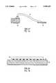
- An example of a typical wirebondis illustrated in FIG. 1a. As shown, a die 10 is bonded to a leadframe or substrate surface 12 by a wire bond 14. While this is a satisfactory implementation, the wafer area required for the bond pads restricts full utilization of wafer dies with increasing feature density on a single die.
- TAB bondingAnother form of interconnection is known as tape automated bonding or TAB bonding.
- the lead frameis bonded to a die by means of a tape placed over the die.
- One side of the tapegoes over the die, while the other side of the tape goes on the leadframe or interconnects to a substrate board.
- Contacts on the dieare plated up, i.e., grown above the circuit, to form "bump" contacts on the IC so that the passivation layers on the die are not cracked by the application of the tape. While this has been used successfully for many years in semiconductor manufacturing, there are risks of cracking the die during the tape application and forming sites of destruction, so that some fabrication facilities have begun to phase it out for cost-effectiveness reasons. Cost is also a factor since custom tapes are needed for each specific chip design.
- flip chip technologyprovides an increased density of possible interconnections on a single die without risking the integrity of the die.
- Flip chip devicesimplement connections directly on the wafer so that the wafer can be "flipped" over, as the name implies, and bonded directly to a substrate, such as bonding to trace pattern wiring pads on a printed circuit board. The bonding is done via solder bumps, i.e., soldered areas formed on top of the die.
- FIG. 1billustrates a chip 16 having solder bumps 18 connecting it to a substrate 20. It is the integrity of these solder bumps that determines the integrity of the interconnection and chip functionality for a given use.
- solder bumpsare formed by depositing a layer of solder into openings over bond pads on a patterned wafer and then etching the areas outside these soldered bond pads to leave the solder bumps 18.
- Solder depositionincludes using evaporation methods, which are expensive and time-consuming, or using plating techniques.
- the etched areasare typically multiple metal cathode layers each of which requires a separate etching and cleaning step for removal.
- aluminum, nickel, and copperare typical metals used for the metal layers. Accordingly, a standard etchant for the copper and nickel layers is a nitric acid solution, while a strongly phosphoric acid (>80% phosphoric acid) solution is commonly used for the aluminum layer.
- the present inventionuses a dilute phosphoric acid solution to remove the metal layers in a more efficient and effective manner without degrading the solder layer. In this way, a simpler, one-step etching process results, which offers less waste production and less chemical consumption.
- a method for forming solder bumpsbegins with a semiconductor wafer that has been patterned with bond pad areas. A plurality of distinct metal layers are then deposited over the wafer. Subsequently, solder is deposited by way of plating through a mask over the metal layers in the bond pad areas. After the removal of the mask, the metal layers outside of the soldered areas are etched using a dilute phosphoric acid solution, which includes phosphoric acid, acetic acid, hydrogen peroxide, and deionized water. By the use of this solution, the metal layers are removed without attacking the soldered areas. Thus, a pattern of solder bumps are formed on the integrated circuit (IC) wafer.
- ICintegrated circuit
- the metal layersinclude distinct layers of aluminum, nickel-vanadium, and copper.
- the aluminum layeris eliminated.
- the composition of the dilute phosphoric acid solutionincludes approximately 1 to 25% phosphoric acid, 63 to 98% deionized water, 1 to 10% acetic acid, and 0.1 to 2% hydrogen peroxide by volume for use in the etching step.
- a single etchantin the form of a dilute phosphoric acid solution, is used to remove the deposited metal layers outside of the soldered areas. This increases the efficiency of forming solder bumps of high integrity, which are suitable for flip chip applications.
- FIG. 1ais an illustration of a wire bond of the prior art
- FIG. 1bis an illustration of a standard solder bumped die inverted on a substrate
- FIG. 2aillustrates an initial substrate with bond pads and passivation layers
- FIG. 2billustrates the substrate of FIG. 2a with the addition of a plurality of metal layers
- FIG. 2cillustrates the substrate of FIG. 2b with a photoresistive mask
- FIG. 2dillustrates the substrate of FIG. 2c with solder deposited through the mask
- FIG. 2eillustrates the substrate of FIG. 2d following the removal of the mask and the metal layers outside of the deposited solder leaving a series of solder bumps
- FIG. 3is a flow diagram illustrating an overall process for forming the solder bumps illustrated in FIG. 2e.
- FIGS. 2a-2eillustrate the step-by-step appearance of a substrate processed in accordance with a method of the present invention, the overall steps of which are presented with reference to FIG. 3.
- FIG. 2aillustrates an initial substrate 30, which may be formed of any suitable material such as a silicon wafer or gallium arsenide wafer that may be patterned to include many layers of features, as is appreciated by those skilled in the art, and that is generically referred to as a substrate for purposes of this description.
- the topmost layer of substrate 30has been patterned to have bond pads 32 and passivation layers 34.
- the bond pads 32are formed by depositing a layer of aluminum (Al) over the substrate 30 and patterning the layer to form the bond pads 32.
- the passivation layers 34preferably include silicon dioxide deposited by chemical vapor deposition (CVD) or other suitable methods as is well known to those skilled in the art.
- the passivation layersare etched using standard techniques from the bond pads 32, so that the bond pads 32 are exposed for subsequent interconnecting.
- FIG. 2billustrates the addition of metal layers 36, 38, and 40 over the passivation layers 34 and bond pads 32.
- the substratecompleted through passivation, is ashed, wet cleaned, sputter etched, and sputter deposited.
- the first layermay be an approximately 4 kiloAngstrom (k ⁇ ) layer of aluminum (Al) for layer 36, which acts as an adhesive layer.
- An approximately 2 k ⁇ layer of nickel-vanadium (NiV)is then deposited for layer 38 to act as a barrier layer to prevent migration between the surrounding metal layers.
- the NiVcomprises approximately 93% nickel and 7% vanadium.
- An approximately 4 k ⁇ layer of copper (Cu)then follows for layer 40, which acts as a cathode layer for subsequent solder plating.
- the thickness of these layersmay be varied in accordance with the needs of a particular system.
- FIG. 2dillustrates the solder-filled areas 46 formed by plating solder over the metal layers on the bond pads.
- solder plating stepsolder having in the range of approximately 60-95% lead and 5-40% tin has been found to work well.
- layer 40acts as the cathode in order to seed the solder deposition, as is well known to those skilled in the art.
- solder bumps 48solder bumps 48, as shown in FIG. 2e.
- the composition of this dilute phosphoric acid solutionis preferably approximately in the range of 1 to 25% by volume phosphoric acid, 1 to 10% by volume acetic acid, 0.1 to 2% by volume hydrogen peroxide, and 63 to 98% by volume deionized (DI) water.
- etching times approximately in the range of 90 to 600 secondsare appropriate, with 130 seconds having been found to work well, when the solution is approximately 10% phosphoric acid, 5% acetic acid, 1% hydrogen peroxide, and 84% DI water.
- the etchingmay be performed at a wide variety of temperatures, and the temperature used will in turn affect the appropriate duration of the etch, as is appreciated by those skilled in the art.
- the dilute phosphoric acid solutiondoes not attack the solder layer as other standard acid etchant solutions do.
- these other standard solutionsinclude a nickel/copper acid etchant and an acid solution used for aluminum etching.
- the nickel/copper acid etchanta dilute nitric acid solution
- the aluminum etchanta strongly phosphoric acid solution
- FIG. 3is a flow diagram illustrating the overall steps (shown in FIGS. 2a-2e) for forming a series of solder bumps.
- the processbegins in step 100 with wafers which have been processed up through passivation layering (see FIG. 2a).
- step 102is the formation of a plurality of metal layers, as shown in FIG. 2b.
- the waferis first ashed and then wet cleaned, sputter etched, and sputter deposited, as previously described.
- a layer to approximately 4 k ⁇ of aluminum (Al)may be first sputter deposited, followed by an approximately 2 k ⁇ layer of nickel vanadium (NiV) and an approximately 4 k ⁇ layer of copper (Cu).
- a layer of photoresistis then deposited over the wafer in step 104. This layer is then patterned by standard photolithographic techniques to open the bond pad areas of the wafer, as shown in FIG. 2c. Following an ashing and wet clean, solder is plated into the openings of the photoresist to build up the bumps in step 106 (e.g., FIG. 2d). Upon the completion of the plating, the photoresist is stripped using standard techniques in step 108.
- step 110is the etching of the sputter deposited metal layers outside of the soldered areas.
- each layeri.e., the Cu layer, the NiV layer, and the Al layer
- a cleaning stepperformed in between each etch.
- all three metal layersare etched during one step using a dilute phosphoric acid solution.
- the preferable composition of this solutionis approximately in the range of 1 to 25% phosphoric acid by volume, 1 to 10% acetic acid by volume, 0.1 to 2% hydrogen peroxide by volume, and the remaining balance 63 to 98% deionized (DI) water by volume.
- DIdeionized
- the aluminum layer acting as the adhesive layer in the three metal layer arrangementmay be eliminated.
- the remaining metal layer thicknessesare preferably adjusted to maintain a total thickness approximately equal to the three layer thickness, e.g., 1 micron.
- the seed layer of copperis replaced by gold.
- the etching sequenceis slightly altered.
- the gold layeris first removed using potassium cyanide (KCN) applied for approximately 60 seconds at an approximate temperature of 40° C., for example, before the dilute phosphoric acid solution is used to etch the remaining metal layers.
- KCNpotassium cyanide
- duration and temperature of the etchingare interrelated.
- increases in the duration of etchingcorrespond to decreases in etching temperature or decreases in phosphoric acid concentration.
- the etching timeis approximately 600 seconds, while the solution having approximately 10% by volume phosphoric acid requires etching for approximately 130 seconds and the solution having approximately 25% by volume phosphoric acid requires etching for approximately 90 seconds.
- the described solutionhas more than approximately 32% by volume phosphoric acid, no discernible etching of metal layer NiV occurs.
Landscapes
- Engineering & Computer Science (AREA)
- Chemical & Material Sciences (AREA)
- Computer Hardware Design (AREA)
- Power Engineering (AREA)
- Microelectronics & Electronic Packaging (AREA)
- Mechanical Engineering (AREA)
- Chemical Kinetics & Catalysis (AREA)
- General Chemical & Material Sciences (AREA)
- Materials Engineering (AREA)
- Metallurgy (AREA)
- Organic Chemistry (AREA)
- Manufacturing & Machinery (AREA)
- General Physics & Mathematics (AREA)
- Condensed Matter Physics & Semiconductors (AREA)
- Physics & Mathematics (AREA)
- Internal Circuitry In Semiconductor Integrated Circuit Devices (AREA)
- Wire Bonding (AREA)
- ing And Chemical Polishing (AREA)
Abstract
Description
This invention relates generally to etching processes in semiconductor wafer processing and more specifically to solder bump processing in flip chip technology.
The formation of integrated circuit (IC) chips involves many processes. From design to production, each aspect requires considerable attention to detail and precision to create and maintain a high yield of functioning chips. One such aspect is the method employed for interconnection and packaging of a patterned wafer die.
A traditional method of input-output (I/O) interconnection is wirebonding. This involves the bonding of I/O pads around the periphery of the wafer die with wires on a leadframe, followed by encapsulation into a chip package or packaging in a cavity-type package. An example of a typical wirebond is illustrated in FIG. 1a. As shown, a die 10 is bonded to a leadframe orsubstrate surface 12 by awire bond 14. While this is a satisfactory implementation, the wafer area required for the bond pads restricts full utilization of wafer dies with increasing feature density on a single die.
Another form of interconnection is known as tape automated bonding or TAB bonding. In this method, the lead frame is bonded to a die by means of a tape placed over the die. One side of the tape goes over the die, while the other side of the tape goes on the leadframe or interconnects to a substrate board. Contacts on the die are plated up, i.e., grown above the circuit, to form "bump" contacts on the IC so that the passivation layers on the die are not cracked by the application of the tape. While this has been used successfully for many years in semiconductor manufacturing, there are risks of cracking the die during the tape application and forming sites of destruction, so that some fabrication facilities have begun to phase it out for cost-effectiveness reasons. Cost is also a factor since custom tapes are needed for each specific chip design.
Alternatively, flip chip technology provides an increased density of possible interconnections on a single die without risking the integrity of the die. Flip chip devices implement connections directly on the wafer so that the wafer can be "flipped" over, as the name implies, and bonded directly to a substrate, such as bonding to trace pattern wiring pads on a printed circuit board. The bonding is done via solder bumps, i.e., soldered areas formed on top of the die. FIG. 1b illustrates achip 16 havingsolder bumps 18 connecting it to asubstrate 20. It is the integrity of these solder bumps that determines the integrity of the interconnection and chip functionality for a given use.
In prior art practices, these solder bumps are formed by depositing a layer of solder into openings over bond pads on a patterned wafer and then etching the areas outside these soldered bond pads to leave thesolder bumps 18. Solder deposition includes using evaporation methods, which are expensive and time-consuming, or using plating techniques. The etched areas are typically multiple metal cathode layers each of which requires a separate etching and cleaning step for removal. For example, aluminum, nickel, and copper are typical metals used for the metal layers. Accordingly, a standard etchant for the copper and nickel layers is a nitric acid solution, while a strongly phosphoric acid (>80% phosphoric acid) solution is commonly used for the aluminum layer. These etchants have been found to attack the applied solder, making them less than ideal for solder bump formation. Further, each time the wafer is etched and cleaned to remove each of the metal layers, there is an increased risk of contamination and degradation of the solder bumps, so that every added step increases production time and cost. Therefore, in a continuing effort to improve upon solder bump formation, the present invention uses a dilute phosphoric acid solution to remove the metal layers in a more efficient and effective manner without degrading the solder layer. In this way, a simpler, one-step etching process results, which offers less waste production and less chemical consumption.
In accordance with the present invention, a method for forming solder bumps begins with a semiconductor wafer that has been patterned with bond pad areas. A plurality of distinct metal layers are then deposited over the wafer. Subsequently, solder is deposited by way of plating through a mask over the metal layers in the bond pad areas. After the removal of the mask, the metal layers outside of the soldered areas are etched using a dilute phosphoric acid solution, which includes phosphoric acid, acetic acid, hydrogen peroxide, and deionized water. By the use of this solution, the metal layers are removed without attacking the soldered areas. Thus, a pattern of solder bumps are formed on the integrated circuit (IC) wafer.
In one embodiment, the metal layers include distinct layers of aluminum, nickel-vanadium, and copper. In an alternate embodiment, the aluminum layer is eliminated. By way of example, the composition of the dilute phosphoric acid solution includes approximately 1 to 25% phosphoric acid, 63 to 98% deionized water, 1 to 10% acetic acid, and 0.1 to 2% hydrogen peroxide by volume for use in the etching step.
With the present invention, a single etchant, in the form of a dilute phosphoric acid solution, is used to remove the deposited metal layers outside of the soldered areas. This increases the efficiency of forming solder bumps of high integrity, which are suitable for flip chip applications.
The invention, together with further objects and advantages thereof, may best be understood by reference to the following description taken in conjunction with the accompanying drawings in which:
FIG. 1a is an illustration of a wire bond of the prior art;
FIG. 1b is an illustration of a standard solder bumped die inverted on a substrate;
FIG. 2a illustrates an initial substrate with bond pads and passivation layers;
FIG. 2b illustrates the substrate of FIG. 2a with the addition of a plurality of metal layers;
FIG. 2c illustrates the substrate of FIG. 2b with a photoresistive mask;
FIG. 2d illustrates the substrate of FIG. 2c with solder deposited through the mask;
FIG. 2e illustrates the substrate of FIG. 2d following the removal of the mask and the metal layers outside of the deposited solder leaving a series of solder bumps; and
FIG. 3 is a flow diagram illustrating an overall process for forming the solder bumps illustrated in FIG. 2e.
The present invention relates to solder bump formation for use in flip chip IC interconnection. FIGS. 2a-2e illustrate the step-by-step appearance of a substrate processed in accordance with a method of the present invention, the overall steps of which are presented with reference to FIG. 3.
FIG. 2a illustrates aninitial substrate 30, which may be formed of any suitable material such as a silicon wafer or gallium arsenide wafer that may be patterned to include many layers of features, as is appreciated by those skilled in the art, and that is generically referred to as a substrate for purposes of this description. The topmost layer ofsubstrate 30 has been patterned to havebond pads 32 and passivation layers 34. Thebond pads 32 are formed by depositing a layer of aluminum (Al) over thesubstrate 30 and patterning the layer to form thebond pads 32. The passivation layers 34 preferably include silicon dioxide deposited by chemical vapor deposition (CVD) or other suitable methods as is well known to those skilled in the art. The passivation layers are etched using standard techniques from thebond pads 32, so that thebond pads 32 are exposed for subsequent interconnecting.
FIG. 2b illustrates the addition ofmetal layers bond pads 32. For the application of metal layers 36-40, the substrate, completed through passivation, is ashed, wet cleaned, sputter etched, and sputter deposited. By way of example, the first layer may be an approximately 4 kiloAngstrom (kÅ) layer of aluminum (Al) forlayer 36, which acts as an adhesive layer. An approximately 2 kÅ layer of nickel-vanadium (NiV) is then deposited forlayer 38 to act as a barrier layer to prevent migration between the surrounding metal layers. Typically, the NiV comprises approximately 93% nickel and 7% vanadium. An approximately 4 kÅ layer of copper (Cu) then follows forlayer 40, which acts as a cathode layer for subsequent solder plating. Of course, the thickness of these layers may be varied in accordance with the needs of a particular system.
Following the deposition of the metal layers 36-40, a layer ofphotoresistive material 42 is deposited andopenings 44 are developed over the bond pad areas by standard photolithographic techniques, the results of which are illustrated in FIG. 2c. Theopenings 44 expose the areas in which the solder is to be plated. FIG. 2d illustrates the solder-filledareas 46 formed by plating solder over the metal layers on the bond pads. A wide variety of lead/tin solders may be used in the solder plating step. By way of example, solder having in the range of approximately 60-95% lead and 5-40% tin has been found to work well. During the plating process, layer 40 acts as the cathode in order to seed the solder deposition, as is well known to those skilled in the art.
Once the solder has been plated through theopenings 44, the photoresistive material is removed in a stripper by standard removal techniques. All of the metal layers 36-40 outside of the solder-filledareas 46 are then etched using a dilute phosphoric acid solution to leavesolder bumps 48, as shown in FIG. 2e. The composition of this dilute phosphoric acid solution is preferably approximately in the range of 1 to 25% by volume phosphoric acid, 1 to 10% by volume acetic acid, 0.1 to 2% by volume hydrogen peroxide, and 63 to 98% by volume deionized (DI) water. By way of example, when the etching is done at about 70° C., etching times approximately in the range of 90 to 600 seconds are appropriate, with 130 seconds having been found to work well, when the solution is approximately 10% phosphoric acid, 5% acetic acid, 1% hydrogen peroxide, and 84% DI water. Of course, the etching may be performed at a wide variety of temperatures, and the temperature used will in turn affect the appropriate duration of the etch, as is appreciated by those skilled in the art. When used in this manner, the dilute phosphoric acid solution does not attack the solder layer as other standard acid etchant solutions do.
In comparative experiments, these other standard solutions include a nickel/copper acid etchant and an acid solution used for aluminum etching. As shown in the following table, Table 1, the nickel/copper acid etchant, a dilute nitric acid solution, has approximately 84% DI water, 10% nitric acid, 5% acetic acid, and 1% hydrogen peroxide and is usually applied at about 50° C. The aluminum etchant, a strongly phosphoric acid solution, has approximately 83% phosphoric acid, 11% acetic acid, and 6% DI water and is usually applied at about 60° C. Both of these have been found to attack deposited solder, so that neither of these standard etchants is as well suited for performing the etching that the dilute phosphoric acid solution of the present invention performs.
TABLE 1 ______________________________________ Ni/Cu Etch Al Etch Dilute Phosphoric ______________________________________ DI Water: 84% 6% 86% Acetic Acid: 5% 11% 4% H.sub.2 O.sub.2 : 1% 1% Phosphoric Acid: 83% 9% Nitric Acid: 10% Temperature: 50° C. 60° C. 70° C. ______________________________________
In accordance with the present invention, FIG. 3 is a flow diagram illustrating the overall steps (shown in FIGS. 2a-2e) for forming a series of solder bumps. The process begins instep 100 with wafers which have been processed up through passivation layering (see FIG. 2a). The next step,step 102, is the formation of a plurality of metal layers, as shown in FIG. 2b. The wafer is first ashed and then wet cleaned, sputter etched, and sputter deposited, as previously described. Again, by way of example, a layer to approximately 4 kÅ of aluminum (Al) may be first sputter deposited, followed by an approximately 2 kÅ layer of nickel vanadium (NiV) and an approximately 4 kÅ layer of copper (Cu).
A layer of photoresist is then deposited over the wafer instep 104. This layer is then patterned by standard photolithographic techniques to open the bond pad areas of the wafer, as shown in FIG. 2c. Following an ashing and wet clean, solder is plated into the openings of the photoresist to build up the bumps in step 106 (e.g., FIG. 2d). Upon the completion of the plating, the photoresist is stripped using standard techniques in step 108.
The next step,step 110, is the etching of the sputter deposited metal layers outside of the soldered areas. In prior art practices, each layer, i.e., the Cu layer, the NiV layer, and the Al layer, would have to be etched in separate etching steps with a cleaning step performed in between each etch. In the present invention, all three metal layers are etched during one step using a dilute phosphoric acid solution. Again, the preferable composition of this solution is approximately in the range of 1 to 25% phosphoric acid by volume, 1 to 10% acetic acid by volume, 0.1 to 2% hydrogen peroxide by volume, and the remaining balance 63 to 98% deionized (DI) water by volume. The results of this etching step are shown in FIG. 2e, which illustrates that by this process, solder bumps are formed with one etching step without negatively affecting the size, shape, or integrity of the bump.
In an alternate embodiment, the aluminum layer acting as the adhesive layer in the three metal layer arrangement may be eliminated. For this embodiment, the remaining metal layer thicknesses are preferably adjusted to maintain a total thickness approximately equal to the three layer thickness, e.g., 1 micron.
In another alternate embodiment, the seed layer of copper is replaced by gold. In this case, the etching sequence is slightly altered. The gold layer is first removed using potassium cyanide (KCN) applied for approximately 60 seconds at an approximate temperature of 40° C., for example, before the dilute phosphoric acid solution is used to etch the remaining metal layers.
Although only a few embodiments of the present invention have been described in detail, it should be understood that the present invention may be embodied in many other specific forms without departing from the spirit or scope of the invention. Particularly, the invention has been described in the context of solder deposition involving plating. Alternatively, an evaporation deposition process could also be performed. Further, the composition of the solder may be varied. Although the solder has been described as a lead and tin combination, pure tin solder could also be used.
Further, as will be appreciated by those skilled in the art, variations of the duration and temperature of the etching along with the percentage composition of the etchant components are interrelated. Thus, increases in the duration of etching correspond to decreases in etching temperature or decreases in phosphoric acid concentration. For example, for the solution having approximately 1% by volume phosphoric acid, the etching time is approximately 600 seconds, while the solution having approximately 10% by volume phosphoric acid requires etching for approximately 130 seconds and the solution having approximately 25% by volume phosphoric acid requires etching for approximately 90 seconds. However, when the described solution has more than approximately 32% by volume phosphoric acid, no discernible etching of metal layer NiV occurs.
Claims (29)
1. A method for forming solder bumps on a substrate, said substrate including bond pad areas, the method comprising the steps of:
depositing a plurality of distinct metal layers over said substrate the distinct metal layers being formed from different materials and including at least two layers formed from materials selected from the group consisting of aluminum, copper, and a nickel-vanadium alloy;
depositing solder through a mask over said metal layers in said bond pad areas;
removing said mask; and
etching said metal layers outside of said solder with a dilute phosphoric acid solution consisting of essentially of phosphoric acid, deionized (DI) water, acetic acid, and hydrogen peroxide that does not attack said solder to leave a series of solder bumps on said substrate in said bond pad areas.
2. A method for forming solder bumps on a substrate, said substrate including bond pad areas, the method comprising the steps of:
depositing a plurality of distinct metal layers over said substrate, the distinct metal layers being formed from different materials and including at least two layers formed from materials selected from the group consisting of aluminum, copper, and a nickel-vanadium alloy;
depositing solder through a mask over said metal layers in said bond pad areas;
removing said mask; and
etching said metal layers outside of said solder with a dilute phosphoric acid solution consisting essentially of phosphoric acid, deionized (DI) water, acetic acid, and hydrogen peroxide that does not attack said solder to leave a series of solder bumps on said substrate in said bond pad areas, wherein said dilute phosphoric acid solution includes in a range of approximately 1 to 25% by volume phosphoric acid, in a range of approximately 63 to 98% by volume DI water, in a range of approximately 1 to 10% by volume acetic acid, and in a range of approximately 0.1 to 2% by volume hydrogen peroxide.
3. A method as recited in claim 2 wherein said dilute phosphoric acid solution is applied at approximately 70° C.
4. A method as recited in claim 3 wherein said dilute phosphoric acid solution is applied for approximately in the range of 90 to 600 seconds.
5. A method as recited in claim 1 wherein said dilute phosphoric acid solution includes in the range of approximately 1 to 25% by volume phosphoric acid.
6. A method as recited in claim 5 wherein said dilute phosphoric acid solution includes approximately 10% by volume phosphoric acid.
7. A method as recited in claim 5 wherein said dilute phosphoric acid solution includes in the range of approximately 63 to 98% by volume DI water.
8. A method as recited in claim 7 wherein said dilute phosphoric acid solution includes approximately 84% by volume DI water.
9. A method as recited in claim 7 wherein said dilute phosphoric acid solution includes in the range of approximately 1 to 10% by volume acetic acid.
10. A method as recited in claim 9 wherein said dilute phosphoric acid solution includes approximately 5% by volume acetic acid.
11. A method as recited in claim 2 wherein said dilute phosphoric acid solution includes approximately 1% by volume hydrogen peroxide.
12. A method as recited 1 wherein said metal layers include a layer of aluminum, a layer of nickel-vanadium, and a layer of copper.
13. A method as recited 1 wherein said metal layers include a layer of nickel-vanadium and a layer of copper.
14. A method as recited in claim 1 further comprising a top layer of gold formed over the plurality of distinct metal layers, and wherein said gold layer is etched with potassium cyanide prior to said step of etching with said dilute phosphoric acid solution.
15. A method for forming solder bumps over a substrate having a pattern of bond pad areas and a passivation layer deposited over said substrate and patterned to have openings in said bond pad areas, the method comprising the steps of:
depositing a plurality of distinct metal layers over the substrate, the distinct metal layers being formed from different materials and including at least two layers formed from materials selected from the group consisting of aluminum, copper, and nickel-vanadium alloy;
depositing a photoresistive layer over said metal layers:
developing openings in said photoresistive layer over said bond pad areas on said substrate;
plating solder over said metal layers into said openings;
removing said photoresistive layer; and
etching exposed portions of the metal layers from said substrate outside of said solder with a dilute phosphoric acid solution consisting essentially of phosphoric acid deionized (DI) water, acetic acid, and hydrogen peroxide that does not attack said solder to leave a series of solder bumps on said substrate.
16. A method as recited in claim 15 wherein said step of etching is performed at approximately 70° C.
17. A method as recited in claim 15 wherein said dilute phosphoric acid solution includes in a range of approximately 1 to 25% by volume phosphoric acid.
18. A method as recited in claim 17 wherein said dilute phosphoric acid solution includes approximately 10% by volume phosphoric acid.
19. A method as recited in claim 17 wherein said dilute phosphoric acid solution includes in a range of approximately 63 to 98% by volume DI water.
20. A method as recited in claim 19 wherein said dilute phosphoric acid solution includes approximately 84% by volume DI water.
21. A method as recited in claim 19 wherein said dilute phosphoric acid solution includes in a range of approximately 1 to 10% by volume acetic acid.
22. A method as recited in claim 21 wherein said dilute phosphoric acid solution includes approximately 5% by volume acetic acid.
23. A method as recited in claim 21 wherein said dilute phosphoric acid solution includes in a range of approximately 0.1 to 2% by volume hydrogen peroxide.
24. A method as recited in claim 23 wherein said dilute phosphoric acid solution includes approximately 1% by volume hydrogen peroxide.
25. A method as recited claim 15 wherein said step of depositing further comprises depositing a layer of aluminum over said substrate, depositing a layer of nickel-vanadium over said layer of aluminum, and depositing a layer of copper over said layer of nickel-vanadium.
26. A method as recited claim 15 wherein said step of depositing further comprises depositing a layer of nickel-vanadium over said substrate and depositing a layer of copper over said layer of nickel-vanadium.
27. A method as recited claim 15 wherein said step of depositing further comprises depositing a layer of aluminum over said substrate, depositing a layer of nickel-vanadium over said layer of aluminum, and depositing a layer of gold over said layer of nickel-vanadium, and wherein said method further includes a step of etching said layer of gold with potassium cyanide prior to said step of etching with a dilute phosphoric acid solution.
28. A method as recited in claim 15 wherein said solder comprises lead and tin.
29. A method as recited in claim 28 wherein approximately 60-95% of said solder is lead and approximately 5-40% is tin.
Priority Applications (5)
| Application Number | Priority Date | Filing Date | Title |
|---|---|---|---|
| US08/248,409US5508229A (en) | 1994-05-24 | 1994-05-24 | Method for forming solder bumps in semiconductor devices |
| KR1019960700354AKR100323657B1 (en) | 1994-05-24 | 1995-01-20 | How to Form Soul the Bump |
| DE69512991TDE69512991T2 (en) | 1994-05-24 | 1995-01-20 | SOLDER STOOL PRODUCTION METHOD |
| PCT/US1995/000800WO1995032521A1 (en) | 1994-05-24 | 1995-01-20 | Method for forming solder bumps |
| EP95908602AEP0711454B1 (en) | 1994-05-24 | 1995-01-20 | Method for forming solder bumps |
Applications Claiming Priority (1)
| Application Number | Priority Date | Filing Date | Title |
|---|---|---|---|
| US08/248,409US5508229A (en) | 1994-05-24 | 1994-05-24 | Method for forming solder bumps in semiconductor devices |
Publications (1)
| Publication Number | Publication Date |
|---|---|
| US5508229Atrue US5508229A (en) | 1996-04-16 |
Family
ID=22938989
Family Applications (1)
| Application Number | Title | Priority Date | Filing Date |
|---|---|---|---|
| US08/248,409Expired - LifetimeUS5508229A (en) | 1994-05-24 | 1994-05-24 | Method for forming solder bumps in semiconductor devices |
Country Status (5)
| Country | Link |
|---|---|
| US (1) | US5508229A (en) |
| EP (1) | EP0711454B1 (en) |
| KR (1) | KR100323657B1 (en) |
| DE (1) | DE69512991T2 (en) |
| WO (1) | WO1995032521A1 (en) |
Cited By (110)
| Publication number | Priority date | Publication date | Assignee | Title |
|---|---|---|---|---|
| US5665610A (en)* | 1995-05-19 | 1997-09-09 | Matsushita Electric Industrial Co., Ltd. | Semiconductor device checking method |
| US5759437A (en)* | 1996-10-31 | 1998-06-02 | International Business Machines Corporation | Etching of Ti-W for C4 rework |
| US5767546A (en)* | 1994-12-30 | 1998-06-16 | Siliconix Incorporated | Laternal power mosfet having metal strap layer to reduce distributed resistance |
| US5783868A (en)* | 1996-09-20 | 1998-07-21 | Integrated Device Technology, Inc. | Extended bond pads with a plurality of perforations |
| US5886414A (en)* | 1996-09-20 | 1999-03-23 | Integrated Device Technology, Inc. | Removal of extended bond pads using intermetallics |
| US5963835A (en)* | 1997-02-18 | 1999-10-05 | Micron Technology Inc. | Method of forming aluminum film |
| US6011313A (en)* | 1997-06-23 | 2000-01-04 | Ford Motor Company | Flip chip interconnections on electronic modules |
| US6043125A (en)* | 1994-12-30 | 2000-03-28 | Siliconix Incorporated | Method of fabricating vertical power MOSFET having low distributed resistance |
| EP0849797A3 (en)* | 1996-12-19 | 2000-05-03 | Texas Instruments Incorporated | Improvements in or relating to intergrated circuits |
| US6117299A (en)* | 1997-05-09 | 2000-09-12 | Mcnc | Methods of electroplating solder bumps of uniform height on integrated circuit substrates |
| US6136767A (en)* | 1997-03-03 | 2000-10-24 | Micron Technology, Inc. | Dilute composition cleaning method |
| US6146984A (en)* | 1999-10-08 | 2000-11-14 | Agilent Technologies Inc. | Method and structure for uniform height solder bumps on a semiconductor wafer |
| US6251797B1 (en)* | 1999-02-26 | 2001-06-26 | Rohm Co., Ltd. | Method of fabricating semiconductor device |
| US6251501B1 (en)* | 1999-03-29 | 2001-06-26 | Delphi Technologies, Inc. | Surface mount circuit device and solder bumping method therefor |
| US6313048B1 (en) | 1997-03-03 | 2001-11-06 | Micron Technology, Inc. | Dilute cleaning composition and method for using same |
| US6316830B1 (en) | 1998-12-17 | 2001-11-13 | Charles Wen Chyang Lin | Bumpless flip chip assembly with strips and via-fill |
| US6332988B1 (en) | 1999-06-02 | 2001-12-25 | International Business Machines Corporation | Rework process |
| US6350386B1 (en) | 2000-09-20 | 2002-02-26 | Charles W. C. Lin | Method of making a support circuit with a tapered through-hole for a semiconductor chip assembly |
| US6350632B1 (en) | 2000-09-20 | 2002-02-26 | Charles W. C. Lin | Semiconductor chip assembly with ball bond connection joint |
| US6350633B1 (en) | 2000-08-22 | 2002-02-26 | Charles W. C. Lin | Semiconductor chip assembly with simultaneously electroplated contact terminal and connection joint |
| US6375062B1 (en)* | 2000-11-06 | 2002-04-23 | Delphi Technologies, Inc. | Surface bumping method and structure formed thereby |
| US6403460B1 (en) | 2000-08-22 | 2002-06-11 | Charles W. C. Lin | Method of making a semiconductor chip assembly |
| US6402970B1 (en) | 2000-08-22 | 2002-06-11 | Charles W. C. Lin | Method of making a support circuit for a semiconductor chip assembly |
| US6403400B2 (en) | 1998-12-17 | 2002-06-11 | Charles Wen Chyang Lin | Bumpless flip chip assembly with strips-in-via and plating |
| US6406939B1 (en) | 1998-05-02 | 2002-06-18 | Charles W. C. Lin | Flip chip assembly with via interconnection |
| US6436734B1 (en) | 2000-08-22 | 2002-08-20 | Charles W. C. Lin | Method of making a support circuit for a semiconductor chip assembly |
| US6440835B1 (en) | 2000-10-13 | 2002-08-27 | Charles W. C. Lin | Method of connecting a conductive trace to a semiconductor chip |
| US6444489B1 (en) | 2000-12-15 | 2002-09-03 | Charles W. C. Lin | Semiconductor chip assembly with bumped molded substrate |
| US6448644B1 (en) | 1998-05-02 | 2002-09-10 | Charles W. C. Lin | Flip chip assembly with via interconnection |
| US6448108B1 (en) | 2000-10-02 | 2002-09-10 | Charles W. C. Lin | Method of making a semiconductor chip assembly with a conductive trace subtractively formed before and after chip attachment |
| US20020158335A1 (en)* | 2001-04-30 | 2002-10-31 | Intel Corporation | High performance, low cost microelectronic circuit package with interposer |
| US20020165105A1 (en)* | 2000-05-31 | 2002-11-07 | Micron Technology, Inc. | Cleaning composition useful in semiconductor integrated circuit fabricating |
| US20020173133A1 (en)* | 2001-05-21 | 2002-11-21 | Intel Corporation | Method for packaging a microelectronic device using on-die bond pad expansion |
| US6492252B1 (en) | 2000-10-13 | 2002-12-10 | Bridge Semiconductor Corporation | Method of connecting a bumped conductive trace to a semiconductor chip |
| US6511865B1 (en) | 2000-09-20 | 2003-01-28 | Charles W. C. Lin | Method for forming a ball bond connection joint on a conductive trace and conductive pad in a semiconductor chip assembly |
| US6521970B1 (en) | 2000-09-01 | 2003-02-18 | National Semiconductor Corporation | Chip scale package with compliant leads |
| US6528891B2 (en) | 1998-12-17 | 2003-03-04 | Charles Wen Chyang Lin | Bumpless flip chip assembly with solder via |
| US20030051912A1 (en)* | 2001-04-23 | 2003-03-20 | Dautartas Mindaugas F. | Solder pads and method of making a solder pad |
| US6537851B1 (en) | 2000-10-13 | 2003-03-25 | Bridge Semiconductor Corporation | Method of connecting a bumped compliant conductive trace to a semiconductor chip |
| US6544813B1 (en) | 2000-10-02 | 2003-04-08 | Charles W. C. Lin | Method of making a semiconductor chip assembly with a conductive trace subtractively formed before and after chip attachment |
| US6548393B1 (en) | 2000-10-13 | 2003-04-15 | Charles W. C. Lin | Semiconductor chip assembly with hardened connection joint |
| US6551861B1 (en) | 2000-08-22 | 2003-04-22 | Charles W. C. Lin | Method of making a semiconductor chip assembly by joining the chip to a support circuit with an adhesive |
| US6562657B1 (en) | 2000-08-22 | 2003-05-13 | Charles W. C. Lin | Semiconductor chip assembly with simultaneously electrolessly plated contact terminal and connection joint |
| US6562709B1 (en) | 2000-08-22 | 2003-05-13 | Charles W. C. Lin | Semiconductor chip assembly with simultaneously electroplated contact terminal and connection joint |
| US6576540B2 (en)* | 2001-06-19 | 2003-06-10 | Phoenix Precision Technology Corporation | Method for fabricating substrate within a Ni/Au structure electroplated on electrical contact pads |
| US6576539B1 (en) | 2000-10-13 | 2003-06-10 | Charles W.C. Lin | Semiconductor chip assembly with interlocked conductive trace |
| US6576493B1 (en) | 2000-10-13 | 2003-06-10 | Bridge Semiconductor Corporation | Method of connecting a conductive trace and an insulative base to a semiconductor chip using multiple etch steps |
| US6583040B1 (en) | 2000-10-13 | 2003-06-24 | Bridge Semiconductor Corporation | Method of making a pillar in a laminated structure for a semiconductor chip assembly |
| US6586276B2 (en) | 2001-07-11 | 2003-07-01 | Intel Corporation | Method for fabricating a microelectronic device using wafer-level adhesion layer deposition |
| US20030146191A1 (en)* | 2002-02-07 | 2003-08-07 | Ho-Ming Tong | Etching method for nickel-vanadium alloy |
| US20030157791A1 (en)* | 2002-02-21 | 2003-08-21 | Ho-Ming Tong | Process of fabricating bumps |
| US20030157438A1 (en)* | 2002-02-20 | 2003-08-21 | Ho-Ming Tong | Bump forming process |
| US20030157792A1 (en)* | 2002-02-21 | 2003-08-21 | Ho-Ming Tong | Bump manufacturing method |
| US6614117B1 (en)* | 2002-06-04 | 2003-09-02 | Skyworks Solutions, Inc. | Method for metallization of a semiconductor substrate and related structure |
| US20030166330A1 (en)* | 2002-03-01 | 2003-09-04 | Ho-Ming Tong | Bump fabrication process |
| US6620720B1 (en)* | 2000-04-10 | 2003-09-16 | Agere Systems Inc | Interconnections to copper IC's |
| US6632700B1 (en) | 2002-04-30 | 2003-10-14 | Taiwan Semiconductor Manufacturing Company | Method to form a color image sensor cell while protecting the bonding pad structure from damage |
| US6653170B1 (en) | 2001-02-06 | 2003-11-25 | Charles W. C. Lin | Semiconductor chip assembly with elongated wire ball bonded to chip and electrolessly plated to support circuit |
| US6660626B1 (en) | 2000-08-22 | 2003-12-09 | Charles W. C. Lin | Semiconductor chip assembly with simultaneously electrolessly plated contact terminal and connection joint |
| US6667229B1 (en) | 2000-10-13 | 2003-12-23 | Bridge Semiconductor Corporation | Method of connecting a bumped compliant conductive trace and an insulative base to a semiconductor chip |
| US6699780B1 (en) | 2000-10-13 | 2004-03-02 | Bridge Semiconductor Corporation | Method of connecting a conductive trace to a semiconductor chip using plasma undercut etching |
| US6716739B2 (en)* | 2002-02-19 | 2004-04-06 | Advanced Semiconductor Engineering, Inc. | Bump manufacturing method |
| US6740576B1 (en) | 2000-10-13 | 2004-05-25 | Bridge Semiconductor Corporation | Method of making a contact terminal with a plated metal peripheral sidewall portion for a semiconductor chip assembly |
| US6747359B1 (en) | 1998-03-05 | 2004-06-08 | Micron Technology, Inc. | Residue-free contact openings and methods for fabricating same |
| US6753609B2 (en)* | 2000-08-21 | 2004-06-22 | Siliconware Precision Industries Co., Ltd. | Circuit probing contact pad formed on a bond pad in a flip chip package |
| US20040188378A1 (en)* | 2003-03-25 | 2004-09-30 | Advanced Semiconductor Engineering, Inc. | Bumping process |
| US20040245630A1 (en)* | 2003-06-09 | 2004-12-09 | Min-Lung Huang | [chip structure] |
| US20040266161A1 (en)* | 2003-06-30 | 2004-12-30 | Advanced Semiconductor Engineering, Inc. | Bumping process |
| US20040266163A1 (en)* | 2003-06-30 | 2004-12-30 | Advanced Semiconductor Engineering, Inc. | Bumping process |
| US20050006792A1 (en)* | 1999-04-26 | 2005-01-13 | Fujitsu Limited | Semiconductor device and method of manufacturing the same |
| US6872591B1 (en) | 2000-10-13 | 2005-03-29 | Bridge Semiconductor Corporation | Method of making a semiconductor chip assembly with a conductive trace and a substrate |
| US6876072B1 (en) | 2000-10-13 | 2005-04-05 | Bridge Semiconductor Corporation | Semiconductor chip assembly with chip in substrate cavity |
| US6900532B1 (en) | 2000-09-01 | 2005-05-31 | National Semiconductor Corporation | Wafer level chip scale package |
| US6908788B1 (en) | 2000-10-13 | 2005-06-21 | Bridge Semiconductor Corporation | Method of connecting a conductive trace to a semiconductor chip using a metal base |
| US6930044B1 (en)* | 2004-03-17 | 2005-08-16 | Nan Ya Printed Circuit Board Corporation | Method for fabricating a packaging substrate |
| US6949408B1 (en) | 2000-10-13 | 2005-09-27 | Bridge Semiconductor Corporation | Method of connecting a conductive trace and an insulative base to a semiconductor chip using multiple etch steps |
| US6984576B1 (en) | 2000-10-13 | 2006-01-10 | Bridge Semiconductor Corporation | Method of connecting an additively and subtractively formed conductive trace and an insulative base to a semiconductor chip |
| US20060012024A1 (en)* | 2000-10-13 | 2006-01-19 | Bridge Semiconductor Corporation | Semiconductor chip assembly with metal containment wall and solder terminal |
| US7009297B1 (en) | 2000-10-13 | 2006-03-07 | Bridge Semiconductor Corporation | Semiconductor chip assembly with embedded metal particle |
| US7071089B1 (en) | 2000-10-13 | 2006-07-04 | Bridge Semiconductor Corporation | Method of making a semiconductor chip assembly with a carved bumped terminal |
| US7075186B1 (en) | 2000-10-13 | 2006-07-11 | Bridge Semiconductor Corporation | Semiconductor chip assembly with interlocked contact terminal |
| US7094676B1 (en) | 2000-10-13 | 2006-08-22 | Bridge Semiconductor Corporation | Semiconductor chip assembly with embedded metal pillar |
| US7112521B1 (en) | 2000-10-13 | 2006-09-26 | Bridge Semiconductor Corporation | Method of making a semiconductor chip assembly with a bumped metal pillar |
| US7129113B1 (en) | 2000-10-13 | 2006-10-31 | Bridge Semiconductor Corporation | Method of making a three-dimensional stacked semiconductor package with a metal pillar in an encapsulant aperture |
| US7132741B1 (en) | 2000-10-13 | 2006-11-07 | Bridge Semiconductor Corporation | Semiconductor chip assembly with carved bumped terminal |
| US20060252245A1 (en)* | 2005-05-04 | 2006-11-09 | Chun-Chi Ke | Fabrication method of under bump metallurgy structure |
| US7183658B2 (en) | 2001-09-05 | 2007-02-27 | Intel Corporation | Low cost microelectronic circuit package |
| US7190080B1 (en) | 2000-10-13 | 2007-03-13 | Bridge Semiconductor Corporation | Semiconductor chip assembly with embedded metal pillar |
| WO2007049878A1 (en)* | 2005-10-28 | 2007-05-03 | Phicom Corporation | Probe card and method of fabricating the same |
| US7262082B1 (en) | 2000-10-13 | 2007-08-28 | Bridge Semiconductor Corporation | Method of making a three-dimensional stacked semiconductor package with a metal pillar and a conductive interconnect in an encapsulant aperture |
| DE102006008261A1 (en)* | 2006-02-22 | 2007-08-30 | Fraunhofer-Gesellschaft zur Förderung der angewandten Forschung e.V. | Etching solution for etching layer system, comprising phosphoric acid, nitric acid, de-ionized water and halogen component, which releases halogen ions that contain these components |
| US7264991B1 (en) | 2000-10-13 | 2007-09-04 | Bridge Semiconductor Corporation | Method of connecting a conductive trace to a semiconductor chip using conductive adhesive |
| US7268421B1 (en) | 2004-11-10 | 2007-09-11 | Bridge Semiconductor Corporation | Semiconductor chip assembly with welded metal pillar that includes enlarged ball bond |
| US7319265B1 (en) | 2000-10-13 | 2008-01-15 | Bridge Semiconductor Corporation | Semiconductor chip assembly with precision-formed metal pillar |
| US20080041813A1 (en)* | 2006-08-21 | 2008-02-21 | Atmel Corporation | Methods and compositions for wet etching |
| US20080045035A1 (en)* | 2006-08-17 | 2008-02-21 | Ji-Sung Lee | Etching solution for etching metal layer, etching method using the etching solution, and method of fabricating semiconductor product using the etching solution |
| US7396703B1 (en) | 2003-11-20 | 2008-07-08 | Bridge Semiconductor Corporation | Method of making a semiconductor chip assembly with a bumped terminal and a filler |
| US7446419B1 (en) | 2004-11-10 | 2008-11-04 | Bridge Semiconductor Corporation | Semiconductor chip assembly with welded metal pillar of stacked metal balls |
| US7494843B1 (en) | 2006-12-26 | 2009-02-24 | Bridge Semiconductor Corporation | Method of making a semiconductor chip assembly with thermal conductor and encapsulant grinding |
| US20090091036A1 (en)* | 2007-10-03 | 2009-04-09 | Advanced Semiconductor Engineering, Inc. | Wafer structure with a buffer layer |
| US20090098723A1 (en)* | 2007-10-13 | 2009-04-16 | Wan-Ling Yu | Method Of Forming Metallic Bump On I/O Pad |
| US7538415B1 (en) | 2003-11-20 | 2009-05-26 | Bridge Semiconductor Corporation | Semiconductor chip assembly with bumped terminal, filler and insulative base |
| US7750483B1 (en) | 2004-11-10 | 2010-07-06 | Bridge Semiconductor Corporation | Semiconductor chip assembly with welded metal pillar and enlarged plated contact terminal |
| US7811863B1 (en) | 2006-10-26 | 2010-10-12 | Bridge Semiconductor Corporation | Method of making a semiconductor chip assembly with metal pillar and encapsulant grinding and heat sink attachment |
| US7993983B1 (en) | 2003-11-17 | 2011-08-09 | Bridge Semiconductor Corporation | Method of making a semiconductor chip assembly with chip and encapsulant grinding |
| US20120064712A1 (en)* | 2010-09-14 | 2012-03-15 | Taiwan Semiconductor Manufacturing Company, Ltd. | Method for Reducing UBM Undercut in Metal Bump Structures |
| EP2615638A2 (en) | 2012-01-16 | 2013-07-17 | Yu, Wan-Ling | Semiconductor Package Structure and Method for Manufacturing The Same |
| US8723313B2 (en) | 2012-01-14 | 2014-05-13 | Wan-Ling Yu | Semiconductor package structure and method for manufacturing the same |
| US9029268B2 (en)* | 2012-11-21 | 2015-05-12 | Dynaloy, Llc | Process for etching metals |
| US20160240395A1 (en)* | 2012-12-20 | 2016-08-18 | Intel Corporation | Methods of promoting adhesion between underfill and conductive bumps and structures formed thereby |
Families Citing this family (3)
| Publication number | Priority date | Publication date | Assignee | Title |
|---|---|---|---|---|
| KR100234694B1 (en)* | 1996-10-29 | 1999-12-15 | 김영환 | Manufacturing method of bga package |
| US6875681B1 (en)* | 1997-12-31 | 2005-04-05 | Intel Corporation | Wafer passivation structure and method of fabrication |
| KR102258660B1 (en) | 2013-09-17 | 2021-06-02 | 삼성전자주식회사 | Liquid composition for etching metal containing Cu and method of fabricating a semiconductor device using the same |
Citations (13)
| Publication number | Priority date | Publication date | Assignee | Title |
|---|---|---|---|---|
| US3655544A (en)* | 1970-03-02 | 1972-04-11 | Gen Electric | Refractory metal/refractory metal nitride resistor films |
| JPS55138256A (en)* | 1979-04-13 | 1980-10-28 | Toshiba Corp | Manufacture of semiconductor device |
| JPS57116776A (en)* | 1981-01-14 | 1982-07-20 | Toshiba Corp | Etching solution for nickel |
| EP0261799A1 (en)* | 1986-08-28 | 1988-03-30 | Fujitsu Limited | Method for producing a terminal electrode of a semi-conductor device |
| US4880708A (en)* | 1988-07-05 | 1989-11-14 | Motorola, Inc. | Metallization scheme providing adhesion and barrier properties |
| US4922322A (en)* | 1989-02-09 | 1990-05-01 | National Semiconductor Corporation | Bump structure for reflow bonding of IC devices |
| US5094979A (en)* | 1989-03-03 | 1992-03-10 | Mitsubishi Denki Kabushiki Kaisha | Method of fabricating semiconductor device |
| US5108950A (en)* | 1987-11-18 | 1992-04-28 | Casio Computer Co., Ltd. | Method for forming a bump electrode for a semiconductor device |
| US5118584A (en)* | 1990-06-01 | 1992-06-02 | Eastman Kodak Company | Method of producing microbump circuits for flip chip mounting |
| US5124269A (en)* | 1988-03-05 | 1992-06-23 | Kanegafuchi Kagaku Kogyo Kabushiki | Method of producing a semiconductor device using a wire mask having a specified diameter |
| US5208186A (en)* | 1989-02-09 | 1993-05-04 | National Semiconductor Corporation | Process for reflow bonding of bumps in IC devices |
| US5266156A (en)* | 1992-06-25 | 1993-11-30 | Digital Equipment Corporation | Methods of forming a local interconnect and a high resistor polysilicon load by reacting cobalt with polysilicon |
| US5324683A (en)* | 1993-06-02 | 1994-06-28 | Motorola, Inc. | Method of forming a semiconductor structure having an air region |
- 1994
- 1994-05-24USUS08/248,409patent/US5508229A/ennot_activeExpired - Lifetime
- 1995
- 1995-01-20WOPCT/US1995/000800patent/WO1995032521A1/enactiveIP Right Grant
- 1995-01-20EPEP95908602Apatent/EP0711454B1/ennot_activeExpired - Lifetime
- 1995-01-20DEDE69512991Tpatent/DE69512991T2/ennot_activeExpired - Lifetime
- 1995-01-20KRKR1019960700354Apatent/KR100323657B1/ennot_activeExpired - Lifetime
Patent Citations (13)
| Publication number | Priority date | Publication date | Assignee | Title |
|---|---|---|---|---|
| US3655544A (en)* | 1970-03-02 | 1972-04-11 | Gen Electric | Refractory metal/refractory metal nitride resistor films |
| JPS55138256A (en)* | 1979-04-13 | 1980-10-28 | Toshiba Corp | Manufacture of semiconductor device |
| JPS57116776A (en)* | 1981-01-14 | 1982-07-20 | Toshiba Corp | Etching solution for nickel |
| EP0261799A1 (en)* | 1986-08-28 | 1988-03-30 | Fujitsu Limited | Method for producing a terminal electrode of a semi-conductor device |
| US5108950A (en)* | 1987-11-18 | 1992-04-28 | Casio Computer Co., Ltd. | Method for forming a bump electrode for a semiconductor device |
| US5124269A (en)* | 1988-03-05 | 1992-06-23 | Kanegafuchi Kagaku Kogyo Kabushiki | Method of producing a semiconductor device using a wire mask having a specified diameter |
| US4880708A (en)* | 1988-07-05 | 1989-11-14 | Motorola, Inc. | Metallization scheme providing adhesion and barrier properties |
| US4922322A (en)* | 1989-02-09 | 1990-05-01 | National Semiconductor Corporation | Bump structure for reflow bonding of IC devices |
| US5208186A (en)* | 1989-02-09 | 1993-05-04 | National Semiconductor Corporation | Process for reflow bonding of bumps in IC devices |
| US5094979A (en)* | 1989-03-03 | 1992-03-10 | Mitsubishi Denki Kabushiki Kaisha | Method of fabricating semiconductor device |
| US5118584A (en)* | 1990-06-01 | 1992-06-02 | Eastman Kodak Company | Method of producing microbump circuits for flip chip mounting |
| US5266156A (en)* | 1992-06-25 | 1993-11-30 | Digital Equipment Corporation | Methods of forming a local interconnect and a high resistor polysilicon load by reacting cobalt with polysilicon |
| US5324683A (en)* | 1993-06-02 | 1994-06-28 | Motorola, Inc. | Method of forming a semiconductor structure having an air region |
Cited By (180)
| Publication number | Priority date | Publication date | Assignee | Title |
|---|---|---|---|---|
| US6066877A (en)* | 1994-12-30 | 2000-05-23 | Siliconix Incorporated | Vertical power MOSFET having thick metal layer to reduce distributed resistance |
| US5767546A (en)* | 1994-12-30 | 1998-06-16 | Siliconix Incorporated | Laternal power mosfet having metal strap layer to reduce distributed resistance |
| US5945709A (en)* | 1994-12-30 | 1999-08-31 | Siliconix Incorporated | Integrated circuit die having thick bus to reduce distributed resistance |
| US6159841A (en)* | 1994-12-30 | 2000-12-12 | Siliconix Incorporated | Method of fabricating lateral power MOSFET having metal strap layer to reduce distributed resistance |
| US6043125A (en)* | 1994-12-30 | 2000-03-28 | Siliconix Incorporated | Method of fabricating vertical power MOSFET having low distributed resistance |
| US5665610A (en)* | 1995-05-19 | 1997-09-09 | Matsushita Electric Industrial Co., Ltd. | Semiconductor device checking method |
| US5783868A (en)* | 1996-09-20 | 1998-07-21 | Integrated Device Technology, Inc. | Extended bond pads with a plurality of perforations |
| US5886414A (en)* | 1996-09-20 | 1999-03-23 | Integrated Device Technology, Inc. | Removal of extended bond pads using intermetallics |
| US5759437A (en)* | 1996-10-31 | 1998-06-02 | International Business Machines Corporation | Etching of Ti-W for C4 rework |
| EP0849797A3 (en)* | 1996-12-19 | 2000-05-03 | Texas Instruments Incorporated | Improvements in or relating to intergrated circuits |
| US6809025B2 (en) | 1997-02-18 | 2004-10-26 | Micron Technology, Inc. | Method of making a void-free aluminum film |
| US5963835A (en)* | 1997-02-18 | 1999-10-05 | Micron Technology Inc. | Method of forming aluminum film |
| US6555471B2 (en) | 1997-02-18 | 2003-04-29 | Micron Technology, Inc. | Method of making a void-free aluminum film |
| US6136767A (en)* | 1997-03-03 | 2000-10-24 | Micron Technology, Inc. | Dilute composition cleaning method |
| US6596647B2 (en) | 1997-03-03 | 2003-07-22 | Micron Technology, Inc. | Dilute cleaning composition and method for using the same |
| US6384001B2 (en) | 1997-03-03 | 2002-05-07 | Micron Technology, Inc. | Dilute cleaning composition |
| US6313048B1 (en) | 1997-03-03 | 2001-11-06 | Micron Technology, Inc. | Dilute cleaning composition and method for using same |
| US6841525B2 (en) | 1997-03-03 | 2005-01-11 | Micron Technology, Inc. | Dilute cleaning composition and method for using same |
| US6117299A (en)* | 1997-05-09 | 2000-09-12 | Mcnc | Methods of electroplating solder bumps of uniform height on integrated circuit substrates |
| US6011313A (en)* | 1997-06-23 | 2000-01-04 | Ford Motor Company | Flip chip interconnections on electronic modules |
| US6250541B1 (en) | 1997-06-23 | 2001-06-26 | Visteon Global Technologies, Inc. | Method of forming interconnections on electronic modules |
| US6747359B1 (en) | 1998-03-05 | 2004-06-08 | Micron Technology, Inc. | Residue-free contact openings and methods for fabricating same |
| US7700497B2 (en) | 1998-03-05 | 2010-04-20 | Micron Technology, Inc. | Methods for fabricating residue-free contact openings |
| US20090104767A1 (en)* | 1998-03-05 | 2009-04-23 | Micron Technology, Inc. | Methods for fabricating residue-free contact openings |
| US7470631B1 (en) | 1998-03-05 | 2008-12-30 | Micron Technology, Inc. | Methods for fabricating residue-free contact openings |
| US6828228B2 (en)* | 1998-03-05 | 2004-12-07 | Micron Technology, Inc. | Methods for fabricating residue-free contact openings |
| US6406939B1 (en) | 1998-05-02 | 2002-06-18 | Charles W. C. Lin | Flip chip assembly with via interconnection |
| US6448644B1 (en) | 1998-05-02 | 2002-09-10 | Charles W. C. Lin | Flip chip assembly with via interconnection |
| US6475833B2 (en) | 1998-12-17 | 2002-11-05 | Charles Wen Chyang Lin | Bumpless flip chip assembly with strips and via-fill |
| US6403400B2 (en) | 1998-12-17 | 2002-06-11 | Charles Wen Chyang Lin | Bumpless flip chip assembly with strips-in-via and plating |
| US6437452B2 (en) | 1998-12-17 | 2002-08-20 | Charles Wen Chyang Lin | Bumpless flip chip assembly with strips-in-via and plating |
| US6316830B1 (en) | 1998-12-17 | 2001-11-13 | Charles Wen Chyang Lin | Bumpless flip chip assembly with strips and via-fill |
| US6528891B2 (en) | 1998-12-17 | 2003-03-04 | Charles Wen Chyang Lin | Bumpless flip chip assembly with solder via |
| US6251797B1 (en)* | 1999-02-26 | 2001-06-26 | Rohm Co., Ltd. | Method of fabricating semiconductor device |
| US6251501B1 (en)* | 1999-03-29 | 2001-06-26 | Delphi Technologies, Inc. | Surface mount circuit device and solder bumping method therefor |
| US7276386B2 (en)* | 1999-04-26 | 2007-10-02 | Fujitsu Limited | Semiconductor device and method of manufacturing the same |
| US20050006792A1 (en)* | 1999-04-26 | 2005-01-13 | Fujitsu Limited | Semiconductor device and method of manufacturing the same |
| US6332988B1 (en) | 1999-06-02 | 2001-12-25 | International Business Machines Corporation | Rework process |
| US6268656B1 (en)* | 1999-10-08 | 2001-07-31 | Agilent Technologies, Inc. | Method and structure for uniform height solder bumps on a semiconductor wafer |
| US6146984A (en)* | 1999-10-08 | 2000-11-14 | Agilent Technologies Inc. | Method and structure for uniform height solder bumps on a semiconductor wafer |
| US6620720B1 (en)* | 2000-04-10 | 2003-09-16 | Agere Systems Inc | Interconnections to copper IC's |
| US20020187906A1 (en)* | 2000-05-31 | 2002-12-12 | Micron Technology, Inc. | Cleaning composition useful in semiconductor integrated circuit fabrication |
| US7135444B2 (en) | 2000-05-31 | 2006-11-14 | Micron Technology, Inc. | Cleaning composition useful in semiconductor integrated circuit fabrication |
| US6486108B1 (en) | 2000-05-31 | 2002-11-26 | Micron Technology, Inc. | Cleaning composition useful in semiconductor integrated circuit fabrication |
| US6831047B2 (en) | 2000-05-31 | 2004-12-14 | Micron Technology, Inc. | Cleaning composition useful in semiconductor integrated circuit fabrication |
| US20020165107A1 (en)* | 2000-05-31 | 2002-11-07 | Micron Technology, Inc. | Cleaning composition useful in semiconductor integrated circuit fabrication |
| US20020169089A1 (en)* | 2000-05-31 | 2002-11-14 | Micron Technology, Inc. | Cleaning composition useful in semiconductor integrated circuit fabrication |
| US7067466B2 (en) | 2000-05-31 | 2006-06-27 | Micron Technology, Inc. | Cleaning composition useful in semiconductor integrated circuit fabrication |
| US20020165106A1 (en)* | 2000-05-31 | 2002-11-07 | Micron Technology, Inc. | Cleaning composition useful in semiconductor integrated circuit fabrication |
| US7067465B2 (en) | 2000-05-31 | 2006-06-27 | Micron Technology, Inc. | Cleaning composition useful in semiconductor integrated circuit fabricating |
| US7087561B2 (en) | 2000-05-31 | 2006-08-08 | Micron Technology, Inc. | Cleaning composition useful in semiconductor integrated circuit fabrication |
| US20020165105A1 (en)* | 2000-05-31 | 2002-11-07 | Micron Technology, Inc. | Cleaning composition useful in semiconductor integrated circuit fabricating |
| US6753609B2 (en)* | 2000-08-21 | 2004-06-22 | Siliconware Precision Industries Co., Ltd. | Circuit probing contact pad formed on a bond pad in a flip chip package |
| US6562657B1 (en) | 2000-08-22 | 2003-05-13 | Charles W. C. Lin | Semiconductor chip assembly with simultaneously electrolessly plated contact terminal and connection joint |
| US6551861B1 (en) | 2000-08-22 | 2003-04-22 | Charles W. C. Lin | Method of making a semiconductor chip assembly by joining the chip to a support circuit with an adhesive |
| US6660626B1 (en) | 2000-08-22 | 2003-12-09 | Charles W. C. Lin | Semiconductor chip assembly with simultaneously electrolessly plated contact terminal and connection joint |
| US6436734B1 (en) | 2000-08-22 | 2002-08-20 | Charles W. C. Lin | Method of making a support circuit for a semiconductor chip assembly |
| US6562709B1 (en) | 2000-08-22 | 2003-05-13 | Charles W. C. Lin | Semiconductor chip assembly with simultaneously electroplated contact terminal and connection joint |
| US6402970B1 (en) | 2000-08-22 | 2002-06-11 | Charles W. C. Lin | Method of making a support circuit for a semiconductor chip assembly |
| US6350633B1 (en) | 2000-08-22 | 2002-02-26 | Charles W. C. Lin | Semiconductor chip assembly with simultaneously electroplated contact terminal and connection joint |
| US6403460B1 (en) | 2000-08-22 | 2002-06-11 | Charles W. C. Lin | Method of making a semiconductor chip assembly |
| US6900110B1 (en) | 2000-09-01 | 2005-05-31 | National Semiconductor Corporation | Chip scale package with compliant leads |
| US6900532B1 (en) | 2000-09-01 | 2005-05-31 | National Semiconductor Corporation | Wafer level chip scale package |
| US6521970B1 (en) | 2000-09-01 | 2003-02-18 | National Semiconductor Corporation | Chip scale package with compliant leads |
| US7241643B1 (en) | 2000-09-01 | 2007-07-10 | National Semiconductor Corporation | Wafer level chip scale package |
| US6511865B1 (en) | 2000-09-20 | 2003-01-28 | Charles W. C. Lin | Method for forming a ball bond connection joint on a conductive trace and conductive pad in a semiconductor chip assembly |
| US6350632B1 (en) | 2000-09-20 | 2002-02-26 | Charles W. C. Lin | Semiconductor chip assembly with ball bond connection joint |
| US6350386B1 (en) | 2000-09-20 | 2002-02-26 | Charles W. C. Lin | Method of making a support circuit with a tapered through-hole for a semiconductor chip assembly |
| US6627824B1 (en) | 2000-09-20 | 2003-09-30 | Charles W. C. Lin | Support circuit with a tapered through-hole for a semiconductor chip assembly |
| US6448108B1 (en) | 2000-10-02 | 2002-09-10 | Charles W. C. Lin | Method of making a semiconductor chip assembly with a conductive trace subtractively formed before and after chip attachment |
| US6544813B1 (en) | 2000-10-02 | 2003-04-08 | Charles W. C. Lin | Method of making a semiconductor chip assembly with a conductive trace subtractively formed before and after chip attachment |
| US7015128B1 (en) | 2000-10-13 | 2006-03-21 | Bridge Semiconductor Corporation | Method of making a semiconductor chip assembly with an embedded metal particle |
| US7232707B1 (en) | 2000-10-13 | 2007-06-19 | Bridge Semiconductor Corporation | Method of making a semiconductor chip assembly with an interlocked contact terminal |
| US6492252B1 (en) | 2000-10-13 | 2002-12-10 | Bridge Semiconductor Corporation | Method of connecting a bumped conductive trace to a semiconductor chip |
| US7071089B1 (en) | 2000-10-13 | 2006-07-04 | Bridge Semiconductor Corporation | Method of making a semiconductor chip assembly with a carved bumped terminal |
| US6653217B1 (en) | 2000-10-13 | 2003-11-25 | Charles W. C. Lin | Method of connecting a conductive trace to a semiconductor chip |
| US6653742B1 (en) | 2000-10-13 | 2003-11-25 | Charles W. C. Lin | Semiconductor chip assembly with interlocked conductive trace |
| US7094676B1 (en) | 2000-10-13 | 2006-08-22 | Bridge Semiconductor Corporation | Semiconductor chip assembly with embedded metal pillar |
| US7419851B2 (en) | 2000-10-13 | 2008-09-02 | Bridge Semiconductor Corporation | Method of making a semiconductor chip assembly with a metal containment wall and a solder terminal |
| US6667229B1 (en) | 2000-10-13 | 2003-12-23 | Bridge Semiconductor Corporation | Method of connecting a bumped compliant conductive trace and an insulative base to a semiconductor chip |
| US6673710B1 (en) | 2000-10-13 | 2004-01-06 | Bridge Semiconductor Corporation | Method of connecting a conductive trace and an insulative base to a semiconductor chip |
| US6699780B1 (en) | 2000-10-13 | 2004-03-02 | Bridge Semiconductor Corporation | Method of connecting a conductive trace to a semiconductor chip using plasma undercut etching |
| US7414319B2 (en) | 2000-10-13 | 2008-08-19 | Bridge Semiconductor Corporation | Semiconductor chip assembly with metal containment wall and solder terminal |
| US6740576B1 (en) | 2000-10-13 | 2004-05-25 | Bridge Semiconductor Corporation | Method of making a contact terminal with a plated metal peripheral sidewall portion for a semiconductor chip assembly |
| US7071573B1 (en) | 2000-10-13 | 2006-07-04 | Bridge Semiconductor Corporation | Semiconductor chip assembly with welded metal pillar |
| US7319265B1 (en) | 2000-10-13 | 2008-01-15 | Bridge Semiconductor Corporation | Semiconductor chip assembly with precision-formed metal pillar |
| US6576539B1 (en) | 2000-10-13 | 2003-06-10 | Charles W.C. Lin | Semiconductor chip assembly with interlocked conductive trace |
| US6800506B1 (en) | 2000-10-13 | 2004-10-05 | Bridge Semiconductor Corporation | Method of making a bumped terminal in a laminated structure for a semiconductor chip assembly |
| US6809414B1 (en) | 2000-10-13 | 2004-10-26 | Bridge Semiconductor Corporation | Semiconductor chip assembly with bumped conductive trace |
| US6440835B1 (en) | 2000-10-13 | 2002-08-27 | Charles W. C. Lin | Method of connecting a conductive trace to a semiconductor chip |
| US7264991B1 (en) | 2000-10-13 | 2007-09-04 | Bridge Semiconductor Corporation | Method of connecting a conductive trace to a semiconductor chip using conductive adhesive |
| US7262082B1 (en) | 2000-10-13 | 2007-08-28 | Bridge Semiconductor Corporation | Method of making a three-dimensional stacked semiconductor package with a metal pillar and a conductive interconnect in an encapsulant aperture |
| US6537851B1 (en) | 2000-10-13 | 2003-03-25 | Bridge Semiconductor Corporation | Method of connecting a bumped compliant conductive trace to a semiconductor chip |
| US7232706B1 (en) | 2000-10-13 | 2007-06-19 | Bridge Semiconductor Corporation | Method of making a semiconductor chip assembly with a precision-formed metal pillar |
| US7075186B1 (en) | 2000-10-13 | 2006-07-11 | Bridge Semiconductor Corporation | Semiconductor chip assembly with interlocked contact terminal |
| US6608374B1 (en) | 2000-10-13 | 2003-08-19 | Bridge Semiconductor Corporation | Semiconductor chip assembly with bumped conductive trace |
| US7190080B1 (en) | 2000-10-13 | 2007-03-13 | Bridge Semiconductor Corporation | Semiconductor chip assembly with embedded metal pillar |
| US6872591B1 (en) | 2000-10-13 | 2005-03-29 | Bridge Semiconductor Corporation | Method of making a semiconductor chip assembly with a conductive trace and a substrate |
| US6876072B1 (en) | 2000-10-13 | 2005-04-05 | Bridge Semiconductor Corporation | Semiconductor chip assembly with chip in substrate cavity |
| US6548393B1 (en) | 2000-10-13 | 2003-04-15 | Charles W. C. Lin | Semiconductor chip assembly with hardened connection joint |
| US7132741B1 (en) | 2000-10-13 | 2006-11-07 | Bridge Semiconductor Corporation | Semiconductor chip assembly with carved bumped terminal |
| US7129575B1 (en) | 2000-10-13 | 2006-10-31 | Bridge Semiconductor Corporation | Semiconductor chip assembly with bumped metal pillar |
| US7067911B1 (en) | 2000-10-13 | 2006-06-27 | Bridge Semiconductor Corporation | Three-dimensional stacked semiconductor package with metal pillar in encapsulant aperture |
| US6908788B1 (en) | 2000-10-13 | 2005-06-21 | Bridge Semiconductor Corporation | Method of connecting a conductive trace to a semiconductor chip using a metal base |
| US7129113B1 (en) | 2000-10-13 | 2006-10-31 | Bridge Semiconductor Corporation | Method of making a three-dimensional stacked semiconductor package with a metal pillar in an encapsulant aperture |
| US6949408B1 (en) | 2000-10-13 | 2005-09-27 | Bridge Semiconductor Corporation | Method of connecting a conductive trace and an insulative base to a semiconductor chip using multiple etch steps |
| US6984576B1 (en) | 2000-10-13 | 2006-01-10 | Bridge Semiconductor Corporation | Method of connecting an additively and subtractively formed conductive trace and an insulative base to a semiconductor chip |
| US20060012024A1 (en)* | 2000-10-13 | 2006-01-19 | Bridge Semiconductor Corporation | Semiconductor chip assembly with metal containment wall and solder terminal |
| US20060014316A1 (en)* | 2000-10-13 | 2006-01-19 | Bridge Semiconductor Corporation | Method of making a semiconductor chip assemby with a metal containment wall and a solder terminal |
| US7112521B1 (en) | 2000-10-13 | 2006-09-26 | Bridge Semiconductor Corporation | Method of making a semiconductor chip assembly with a bumped metal pillar |
| US7009297B1 (en) | 2000-10-13 | 2006-03-07 | Bridge Semiconductor Corporation | Semiconductor chip assembly with embedded metal particle |
| US6583040B1 (en) | 2000-10-13 | 2003-06-24 | Bridge Semiconductor Corporation | Method of making a pillar in a laminated structure for a semiconductor chip assembly |
| US6576493B1 (en) | 2000-10-13 | 2003-06-10 | Bridge Semiconductor Corporation | Method of connecting a conductive trace and an insulative base to a semiconductor chip using multiple etch steps |
| US6375062B1 (en)* | 2000-11-06 | 2002-04-23 | Delphi Technologies, Inc. | Surface bumping method and structure formed thereby |
| US6444489B1 (en) | 2000-12-15 | 2002-09-03 | Charles W. C. Lin | Semiconductor chip assembly with bumped molded substrate |
| US6653170B1 (en) | 2001-02-06 | 2003-11-25 | Charles W. C. Lin | Semiconductor chip assembly with elongated wire ball bonded to chip and electrolessly plated to support circuit |
| US6902098B2 (en) | 2001-04-23 | 2005-06-07 | Shipley Company, L.L.C. | Solder pads and method of making a solder pad |
| US20030051912A1 (en)* | 2001-04-23 | 2003-03-20 | Dautartas Mindaugas F. | Solder pads and method of making a solder pad |
| US6888240B2 (en) | 2001-04-30 | 2005-05-03 | Intel Corporation | High performance, low cost microelectronic circuit package with interposer |
| US20020158335A1 (en)* | 2001-04-30 | 2002-10-31 | Intel Corporation | High performance, low cost microelectronic circuit package with interposer |
| US20020173133A1 (en)* | 2001-05-21 | 2002-11-21 | Intel Corporation | Method for packaging a microelectronic device using on-die bond pad expansion |
| US7071024B2 (en)* | 2001-05-21 | 2006-07-04 | Intel Corporation | Method for packaging a microelectronic device using on-die bond pad expansion |
| US6576540B2 (en)* | 2001-06-19 | 2003-06-10 | Phoenix Precision Technology Corporation | Method for fabricating substrate within a Ni/Au structure electroplated on electrical contact pads |
| US6586276B2 (en) | 2001-07-11 | 2003-07-01 | Intel Corporation | Method for fabricating a microelectronic device using wafer-level adhesion layer deposition |
| US7183658B2 (en) | 2001-09-05 | 2007-02-27 | Intel Corporation | Low cost microelectronic circuit package |
| US20030146191A1 (en)* | 2002-02-07 | 2003-08-07 | Ho-Ming Tong | Etching method for nickel-vanadium alloy |
| US6716739B2 (en)* | 2002-02-19 | 2004-04-06 | Advanced Semiconductor Engineering, Inc. | Bump manufacturing method |
| US20030157438A1 (en)* | 2002-02-20 | 2003-08-21 | Ho-Ming Tong | Bump forming process |
| US6989326B2 (en)* | 2002-02-21 | 2006-01-24 | Advanced Semiconductor Engineering, Inc. | Bump manufacturing method |
| US20030157791A1 (en)* | 2002-02-21 | 2003-08-21 | Ho-Ming Tong | Process of fabricating bumps |
| US20030157792A1 (en)* | 2002-02-21 | 2003-08-21 | Ho-Ming Tong | Bump manufacturing method |
| US6664128B2 (en) | 2002-03-01 | 2003-12-16 | Advanced Semiconductor Engineering, Inc. | Bump fabrication process |
| US20030166330A1 (en)* | 2002-03-01 | 2003-09-04 | Ho-Ming Tong | Bump fabrication process |
| US6632700B1 (en) | 2002-04-30 | 2003-10-14 | Taiwan Semiconductor Manufacturing Company | Method to form a color image sensor cell while protecting the bonding pad structure from damage |
| US6614117B1 (en)* | 2002-06-04 | 2003-09-02 | Skyworks Solutions, Inc. | Method for metallization of a semiconductor substrate and related structure |
| US20040188378A1 (en)* | 2003-03-25 | 2004-09-30 | Advanced Semiconductor Engineering, Inc. | Bumping process |
| US7261828B2 (en) | 2003-03-25 | 2007-08-28 | Advanced Semiconductor Engineering, Inc. | Bumping process |
| US7253519B2 (en)* | 2003-06-09 | 2007-08-07 | Advanced Semiconductor Engineering, Inc. | Chip packaging structure having redistribution layer with recess |
| US20040245630A1 (en)* | 2003-06-09 | 2004-12-09 | Min-Lung Huang | [chip structure] |
| US7112523B2 (en) | 2003-06-30 | 2006-09-26 | Advanced Semiconductor Engineering, Inc. | Bumping process |
| US7091121B2 (en) | 2003-06-30 | 2006-08-15 | Advanced Semiconductor Engineering, Inc. | Bumping process |
| US20040266161A1 (en)* | 2003-06-30 | 2004-12-30 | Advanced Semiconductor Engineering, Inc. | Bumping process |
| US20040266163A1 (en)* | 2003-06-30 | 2004-12-30 | Advanced Semiconductor Engineering, Inc. | Bumping process |
| US7993983B1 (en) | 2003-11-17 | 2011-08-09 | Bridge Semiconductor Corporation | Method of making a semiconductor chip assembly with chip and encapsulant grinding |
| US7453140B1 (en) | 2003-11-20 | 2008-11-18 | Bridge Semiconductor Corporation | Semiconductor chip assembly with laterally aligned filler and insulative base |
| US7459385B1 (en) | 2003-11-20 | 2008-12-02 | Bridge Semiconductor Corporation | Method of making a semiconductor chip assembly with a laterally aligned bumped terminal and filler |
| US7538415B1 (en) | 2003-11-20 | 2009-05-26 | Bridge Semiconductor Corporation | Semiconductor chip assembly with bumped terminal, filler and insulative base |
| US7396703B1 (en) | 2003-11-20 | 2008-07-08 | Bridge Semiconductor Corporation | Method of making a semiconductor chip assembly with a bumped terminal and a filler |
| US7833827B1 (en) | 2003-11-20 | 2010-11-16 | Bridge Semiconductor Corporation | Method of making a semiconductor chip assembly with a bumped terminal, a filler and an insulative base |
| US7417314B1 (en) | 2003-11-20 | 2008-08-26 | Bridge Semiconductor Corporation | Semiconductor chip assembly with laterally aligned bumped terminal and filler |
| US7932165B1 (en) | 2003-11-20 | 2011-04-26 | Bridge Semiconductor Corporation | Method of making a semiconductor chip assembly with a laterally aligned filler and insulative base |
| US7425759B1 (en) | 2003-11-20 | 2008-09-16 | Bridge Semiconductor Corporation | Semiconductor chip assembly with bumped terminal and filler |
| US6930044B1 (en)* | 2004-03-17 | 2005-08-16 | Nan Ya Printed Circuit Board Corporation | Method for fabricating a packaging substrate |
| US7446419B1 (en) | 2004-11-10 | 2008-11-04 | Bridge Semiconductor Corporation | Semiconductor chip assembly with welded metal pillar of stacked metal balls |
| US7750483B1 (en) | 2004-11-10 | 2010-07-06 | Bridge Semiconductor Corporation | Semiconductor chip assembly with welded metal pillar and enlarged plated contact terminal |
| US7268421B1 (en) | 2004-11-10 | 2007-09-11 | Bridge Semiconductor Corporation | Semiconductor chip assembly with welded metal pillar that includes enlarged ball bond |
| US20060252245A1 (en)* | 2005-05-04 | 2006-11-09 | Chun-Chi Ke | Fabrication method of under bump metallurgy structure |
| US7358177B2 (en) | 2005-05-04 | 2008-04-15 | Siliconware Precision Industries Co., Ltd. | Fabrication method of under bump metallurgy structure |
| WO2007049878A1 (en)* | 2005-10-28 | 2007-05-03 | Phicom Corporation | Probe card and method of fabricating the same |
| US7975380B2 (en) | 2005-10-28 | 2011-07-12 | Phicom Corporation | Method of fabricating a probe card |
| US20090184726A1 (en)* | 2005-10-28 | 2009-07-23 | Oug-Ki Lee | Probe card and method of manufacturing the same |
| US20090221152A1 (en)* | 2006-02-22 | 2009-09-03 | Frank Dietz | Etching Solution And Method For Structuring A UBM Layer System |
| WO2007096095A3 (en)* | 2006-02-22 | 2008-02-07 | Fraunhofer Ges Zuer Foerderung | Etching solution and method for structuring a ubm layer system |
| DE102006008261A1 (en)* | 2006-02-22 | 2007-08-30 | Fraunhofer-Gesellschaft zur Förderung der angewandten Forschung e.V. | Etching solution for etching layer system, comprising phosphoric acid, nitric acid, de-ionized water and halogen component, which releases halogen ions that contain these components |
| US20080045035A1 (en)* | 2006-08-17 | 2008-02-21 | Ji-Sung Lee | Etching solution for etching metal layer, etching method using the etching solution, and method of fabricating semiconductor product using the etching solution |
| US20080041813A1 (en)* | 2006-08-21 | 2008-02-21 | Atmel Corporation | Methods and compositions for wet etching |
| US7811863B1 (en) | 2006-10-26 | 2010-10-12 | Bridge Semiconductor Corporation | Method of making a semiconductor chip assembly with metal pillar and encapsulant grinding and heat sink attachment |
| US7494843B1 (en) | 2006-12-26 | 2009-02-24 | Bridge Semiconductor Corporation | Method of making a semiconductor chip assembly with thermal conductor and encapsulant grinding |
| US20090091036A1 (en)* | 2007-10-03 | 2009-04-09 | Advanced Semiconductor Engineering, Inc. | Wafer structure with a buffer layer |
| US7713860B2 (en)* | 2007-10-13 | 2010-05-11 | Wan-Ling Yu | Method of forming metallic bump on I/O pad |
| US20090098723A1 (en)* | 2007-10-13 | 2009-04-16 | Wan-Ling Yu | Method Of Forming Metallic Bump On I/O Pad |
| US20120064712A1 (en)* | 2010-09-14 | 2012-03-15 | Taiwan Semiconductor Manufacturing Company, Ltd. | Method for Reducing UBM Undercut in Metal Bump Structures |
| CN102403243A (en)* | 2010-09-14 | 2012-04-04 | 台湾积体电路制造股份有限公司 | Method for reducing undercut of metal layer under metal bump structure |
| US8389397B2 (en)* | 2010-09-14 | 2013-03-05 | Taiwan Semiconductor Manufacturing Company, Ltd. | Method for reducing UBM undercut in metal bump structures |
| CN102403243B (en)* | 2010-09-14 | 2014-03-12 | 台湾积体电路制造股份有限公司 | Method for reducing undercut phenomenon of metal layer under metal bump structure |
| US8723313B2 (en) | 2012-01-14 | 2014-05-13 | Wan-Ling Yu | Semiconductor package structure and method for manufacturing the same |
| EP2615638A2 (en) | 2012-01-16 | 2013-07-17 | Yu, Wan-Ling | Semiconductor Package Structure and Method for Manufacturing The Same |
| US9029268B2 (en)* | 2012-11-21 | 2015-05-12 | Dynaloy, Llc | Process for etching metals |
| US20160240395A1 (en)* | 2012-12-20 | 2016-08-18 | Intel Corporation | Methods of promoting adhesion between underfill and conductive bumps and structures formed thereby |
| US10115606B2 (en)* | 2012-12-20 | 2018-10-30 | Intel Corporation | Methods of promoting adhesion between underfill and conductive bumps and structures formed thereby |
Also Published As
| Publication number | Publication date |
|---|---|
| KR960705348A (en) | 1996-10-09 |
| KR100323657B1 (en) | 2002-06-24 |
| EP0711454B1 (en) | 1999-10-27 |
| DE69512991T2 (en) | 2000-05-31 |
| DE69512991D1 (en) | 1999-12-02 |
| EP0711454A1 (en) | 1996-05-15 |
| WO1995032521A1 (en) | 1995-11-30 |
Similar Documents
| Publication | Publication Date | Title |
|---|---|---|
| US5508229A (en) | Method for forming solder bumps in semiconductor devices | |
| US5767010A (en) | Solder bump fabrication methods and structure including a titanium barrier layer | |
| KR0166967B1 (en) | Semiconductor device for bonding tape assembly and manufacturing method thereof | |
| US5492235A (en) | Process for single mask C4 solder bump fabrication | |
| EP0261799B1 (en) | Method for producing a terminal electrode of a semi-conductor device | |
| US5277756A (en) | Post fabrication processing of semiconductor chips | |
| US6989326B2 (en) | Bump manufacturing method | |
| KR100278435B1 (en) | Process improvements for titanium-tungsten etching in the presence of electroplated c4's | |
| US5208186A (en) | Process for reflow bonding of bumps in IC devices | |
| US20030006062A1 (en) | Interconnect system and method of fabrication | |
| US20030166330A1 (en) | Bump fabrication process | |
| CN101668830A (en) | Selective etching of TiW for capture pad formation | |
| US6319846B1 (en) | Method for removing solder bodies from a semiconductor wafer | |
| WO2025011481A1 (en) | Double-sided fan-out type packaging method and packaging structure | |
| US20030157438A1 (en) | Bump forming process | |
| US20030157789A1 (en) | Bump manufacturing method | |
| KR20020060307A (en) | Manufacturing method for solder bump | |
| US7443039B2 (en) | System for different bond pads in an integrated circuit package | |
| JPH09148331A (en) | Semiconductor integrated circuit device and method of manufacturing the same | |
| JP2717835B2 (en) | Method for manufacturing semiconductor device | |
| CN1103119C (en) | Method for Single Mask C4 Solder Bump Fabrication | |
| TW556293B (en) | Bump process | |
| JPH09213700A (en) | Manufacturing method of bump electrode | |
| US20060134884A1 (en) | Wafer structure, chip structure, and fabricating process thereof | |
| WO1992011743A2 (en) | An interconnect structure for connecting electronic devices |
Legal Events
| Date | Code | Title | Description |
|---|---|---|---|
| AS | Assignment | Owner name:NATIONAL SEMICONDUCTOR CORPORATION, CALIFORNIA Free format text:ASSIGNMENT OF ASSIGNORS INTEREST;ASSIGNOR:BAKER, MARK H.;REEL/FRAME:007065/0423 Effective date:19940615 | |
| STCF | Information on status: patent grant | Free format text:PATENTED CASE | |
| CC | Certificate of correction | ||
| FEPP | Fee payment procedure | Free format text:PAYOR NUMBER ASSIGNED (ORIGINAL EVENT CODE: ASPN); ENTITY STATUS OF PATENT OWNER: LARGE ENTITY | |
| FPAY | Fee payment | Year of fee payment:4 | |
| FPAY | Fee payment | Year of fee payment:8 | |
| FPAY | Fee payment | Year of fee payment:12 | |
| REMI | Maintenance fee reminder mailed |