US5506383A - Wafer scale multi-chip module - Google Patents
Wafer scale multi-chip moduleDownload PDFInfo
- Publication number
- US5506383A US5506383AUS08/386,893US38689395AUS5506383AUS 5506383 AUS5506383 AUS 5506383AUS 38689395 AUS38689395 AUS 38689395AUS 5506383 AUS5506383 AUS 5506383A
- Authority
- US
- United States
- Prior art keywords
- integrated circuit
- circuit chips
- semiconductor wafer
- interconnect network
- top surface
- Prior art date
- Legal status (The legal status is an assumption and is not a legal conclusion. Google has not performed a legal analysis and makes no representation as to the accuracy of the status listed.)
- Expired - Lifetime
Links
- 239000004065semiconductorSubstances0.000claimsabstractdescription33
- 239000000758substrateSubstances0.000claimsabstractdescription14
- 238000004519manufacturing processMethods0.000claimsdescription16
- 229910000679solderInorganic materials0.000claimsdescription14
- 229910052710siliconInorganic materials0.000claimsdescription9
- 239000010703siliconSubstances0.000claimsdescription9
- XUIMIQQOPSSXEZ-UHFFFAOYSA-NSiliconChemical compound[Si]XUIMIQQOPSSXEZ-UHFFFAOYSA-N0.000claimsdescription8
- 230000013011matingEffects0.000claimsdescription3
- 239000004593EpoxySubstances0.000claimsdescription2
- 239000000126substanceSubstances0.000claimsdescription2
- 238000002161passivationMethods0.000claims2
- BASFCYQUMIYNBI-UHFFFAOYSA-NplatinumChemical compound[Pt]BASFCYQUMIYNBI-UHFFFAOYSA-N0.000description12
- 238000000034methodMethods0.000description8
- 229920001721polyimidePolymers0.000description8
- 239000004642PolyimideSubstances0.000description7
- 239000011651chromiumSubstances0.000description6
- 229910052697platinumInorganic materials0.000description6
- 238000013459approachMethods0.000description5
- 230000017525heat dissipationEffects0.000description5
- 239000010949copperSubstances0.000description4
- 238000005549size reductionMethods0.000description4
- 239000000463materialSubstances0.000description3
- VYZAMTAEIAYCRO-UHFFFAOYSA-NChromiumChemical compound[Cr]VYZAMTAEIAYCRO-UHFFFAOYSA-N0.000description2
- RYGMFSIKBFXOCR-UHFFFAOYSA-NCopperChemical compound[Cu]RYGMFSIKBFXOCR-UHFFFAOYSA-N0.000description2
- 229910052804chromiumInorganic materials0.000description2
- 229910052802copperInorganic materials0.000description2
- 230000002950deficientEffects0.000description2
- PCHJSUWPFVWCPO-UHFFFAOYSA-NgoldChemical compound[Au]PCHJSUWPFVWCPO-UHFFFAOYSA-N0.000description2
- 229910052737goldInorganic materials0.000description2
- 239000010931goldSubstances0.000description2
- 238000012986modificationMethods0.000description2
- 230000004048modificationEffects0.000description2
- 238000004806packaging method and processMethods0.000description2
- 230000008646thermal stressEffects0.000description2
- JBRZTFJDHDCESZ-UHFFFAOYSA-NAsGaChemical compound[As]#[Ga]JBRZTFJDHDCESZ-UHFFFAOYSA-N0.000description1
- 229910001218Gallium arsenideInorganic materials0.000description1
- 230000003466anti-cipated effectEffects0.000description1
- 230000015572biosynthetic processEffects0.000description1
- 238000013461designMethods0.000description1
- 238000005530etchingMethods0.000description1
- 230000010354integrationEffects0.000description1
- 239000000155meltSubstances0.000description1
- 238000002360preparation methodMethods0.000description1
- 150000003376siliconChemical class0.000description1
- 238000012360testing methodMethods0.000description1
Images


Classifications
- H—ELECTRICITY
- H01—ELECTRIC ELEMENTS
- H01L—SEMICONDUCTOR DEVICES NOT COVERED BY CLASS H10
- H01L23/00—Details of semiconductor or other solid state devices
- H01L23/52—Arrangements for conducting electric current within the device in operation from one component to another, i.e. interconnections, e.g. wires, lead frames
- H01L23/538—Arrangements for conducting electric current within the device in operation from one component to another, i.e. interconnections, e.g. wires, lead frames the interconnection structure between a plurality of semiconductor chips being formed on, or in, insulating substrates
- H01L23/5389—Arrangements for conducting electric current within the device in operation from one component to another, i.e. interconnections, e.g. wires, lead frames the interconnection structure between a plurality of semiconductor chips being formed on, or in, insulating substrates the chips being integrally enclosed by the interconnect and support structures
- H—ELECTRICITY
- H01—ELECTRIC ELEMENTS
- H01L—SEMICONDUCTOR DEVICES NOT COVERED BY CLASS H10
- H01L24/00—Arrangements for connecting or disconnecting semiconductor or solid-state bodies; Methods or apparatus related thereto
- H01L24/01—Means for bonding being attached to, or being formed on, the surface to be connected, e.g. chip-to-package, die-attach, "first-level" interconnects; Manufacturing methods related thereto
- H01L24/18—High density interconnect [HDI] connectors; Manufacturing methods related thereto
- H01L24/23—Structure, shape, material or disposition of the high density interconnect connectors after the connecting process
- H01L24/24—Structure, shape, material or disposition of the high density interconnect connectors after the connecting process of an individual high density interconnect connector
- H—ELECTRICITY
- H01—ELECTRIC ELEMENTS
- H01L—SEMICONDUCTOR DEVICES NOT COVERED BY CLASS H10
- H01L24/00—Arrangements for connecting or disconnecting semiconductor or solid-state bodies; Methods or apparatus related thereto
- H01L24/80—Methods for connecting semiconductor or other solid state bodies using means for bonding being attached to, or being formed on, the surface to be connected
- H01L24/82—Methods for connecting semiconductor or other solid state bodies using means for bonding being attached to, or being formed on, the surface to be connected by forming build-up interconnects at chip-level, e.g. for high density interconnects [HDI]
- H—ELECTRICITY
- H01—ELECTRIC ELEMENTS
- H01L—SEMICONDUCTOR DEVICES NOT COVERED BY CLASS H10
- H01L2224/00—Indexing scheme for arrangements for connecting or disconnecting semiconductor or solid-state bodies and methods related thereto as covered by H01L24/00
- H01L2224/01—Means for bonding being attached to, or being formed on, the surface to be connected, e.g. chip-to-package, die-attach, "first-level" interconnects; Manufacturing methods related thereto
- H01L2224/18—High density interconnect [HDI] connectors; Manufacturing methods related thereto
- H01L2224/23—Structure, shape, material or disposition of the high density interconnect connectors after the connecting process
- H01L2224/24—Structure, shape, material or disposition of the high density interconnect connectors after the connecting process of an individual high density interconnect connector
- H01L2224/241—Disposition
- H01L2224/24151—Connecting between a semiconductor or solid-state body and an item not being a semiconductor or solid-state body, e.g. chip-to-substrate, chip-to-passive
- H01L2224/24221—Connecting between a semiconductor or solid-state body and an item not being a semiconductor or solid-state body, e.g. chip-to-substrate, chip-to-passive the body and the item being stacked
- H01L2224/24225—Connecting between a semiconductor or solid-state body and an item not being a semiconductor or solid-state body, e.g. chip-to-substrate, chip-to-passive the body and the item being stacked the item being non-metallic, e.g. insulating substrate with or without metallisation
- H01L2224/24227—Connecting between a semiconductor or solid-state body and an item not being a semiconductor or solid-state body, e.g. chip-to-substrate, chip-to-passive the body and the item being stacked the item being non-metallic, e.g. insulating substrate with or without metallisation the HDI interconnect not connecting to the same level of the item at which the semiconductor or solid-state body is mounted, e.g. the semiconductor or solid-state body being mounted in a cavity or on a protrusion of the item
- H—ELECTRICITY
- H01—ELECTRIC ELEMENTS
- H01L—SEMICONDUCTOR DEVICES NOT COVERED BY CLASS H10
- H01L2924/00—Indexing scheme for arrangements or methods for connecting or disconnecting semiconductor or solid-state bodies as covered by H01L24/00
- H01L2924/01—Chemical elements
- H01L2924/01005—Boron [B]
- H—ELECTRICITY
- H01—ELECTRIC ELEMENTS
- H01L—SEMICONDUCTOR DEVICES NOT COVERED BY CLASS H10
- H01L2924/00—Indexing scheme for arrangements or methods for connecting or disconnecting semiconductor or solid-state bodies as covered by H01L24/00
- H01L2924/01—Chemical elements
- H01L2924/01006—Carbon [C]
- H—ELECTRICITY
- H01—ELECTRIC ELEMENTS
- H01L—SEMICONDUCTOR DEVICES NOT COVERED BY CLASS H10
- H01L2924/00—Indexing scheme for arrangements or methods for connecting or disconnecting semiconductor or solid-state bodies as covered by H01L24/00
- H01L2924/01—Chemical elements
- H01L2924/01019—Potassium [K]
- H—ELECTRICITY
- H01—ELECTRIC ELEMENTS
- H01L—SEMICONDUCTOR DEVICES NOT COVERED BY CLASS H10
- H01L2924/00—Indexing scheme for arrangements or methods for connecting or disconnecting semiconductor or solid-state bodies as covered by H01L24/00
- H01L2924/01—Chemical elements
- H01L2924/01024—Chromium [Cr]
- H—ELECTRICITY
- H01—ELECTRIC ELEMENTS
- H01L—SEMICONDUCTOR DEVICES NOT COVERED BY CLASS H10
- H01L2924/00—Indexing scheme for arrangements or methods for connecting or disconnecting semiconductor or solid-state bodies as covered by H01L24/00
- H01L2924/01—Chemical elements
- H01L2924/01029—Copper [Cu]
- H—ELECTRICITY
- H01—ELECTRIC ELEMENTS
- H01L—SEMICONDUCTOR DEVICES NOT COVERED BY CLASS H10
- H01L2924/00—Indexing scheme for arrangements or methods for connecting or disconnecting semiconductor or solid-state bodies as covered by H01L24/00
- H01L2924/01—Chemical elements
- H01L2924/01033—Arsenic [As]
- H—ELECTRICITY
- H01—ELECTRIC ELEMENTS
- H01L—SEMICONDUCTOR DEVICES NOT COVERED BY CLASS H10
- H01L2924/00—Indexing scheme for arrangements or methods for connecting or disconnecting semiconductor or solid-state bodies as covered by H01L24/00
- H01L2924/01—Chemical elements
- H01L2924/01078—Platinum [Pt]
- H—ELECTRICITY
- H01—ELECTRIC ELEMENTS
- H01L—SEMICONDUCTOR DEVICES NOT COVERED BY CLASS H10
- H01L2924/00—Indexing scheme for arrangements or methods for connecting or disconnecting semiconductor or solid-state bodies as covered by H01L24/00
- H01L2924/01—Chemical elements
- H01L2924/01079—Gold [Au]
- H—ELECTRICITY
- H01—ELECTRIC ELEMENTS
- H01L—SEMICONDUCTOR DEVICES NOT COVERED BY CLASS H10
- H01L2924/00—Indexing scheme for arrangements or methods for connecting or disconnecting semiconductor or solid-state bodies as covered by H01L24/00
- H01L2924/013—Alloys
- H01L2924/014—Solder alloys
- H—ELECTRICITY
- H01—ELECTRIC ELEMENTS
- H01L—SEMICONDUCTOR DEVICES NOT COVERED BY CLASS H10
- H01L2924/00—Indexing scheme for arrangements or methods for connecting or disconnecting semiconductor or solid-state bodies as covered by H01L24/00
- H01L2924/10—Details of semiconductor or other solid state devices to be connected
- H01L2924/1015—Shape
- H01L2924/10155—Shape being other than a cuboid
- H01L2924/10156—Shape being other than a cuboid at the periphery
- H—ELECTRICITY
- H01—ELECTRIC ELEMENTS
- H01L—SEMICONDUCTOR DEVICES NOT COVERED BY CLASS H10
- H01L2924/00—Indexing scheme for arrangements or methods for connecting or disconnecting semiconductor or solid-state bodies as covered by H01L24/00
- H01L2924/10—Details of semiconductor or other solid state devices to be connected
- H01L2924/1015—Shape
- H01L2924/10155—Shape being other than a cuboid
- H01L2924/10158—Shape being other than a cuboid at the passive surface
- H—ELECTRICITY
- H01—ELECTRIC ELEMENTS
- H01L—SEMICONDUCTOR DEVICES NOT COVERED BY CLASS H10
- H01L2924/00—Indexing scheme for arrangements or methods for connecting or disconnecting semiconductor or solid-state bodies as covered by H01L24/00
- H01L2924/10—Details of semiconductor or other solid state devices to be connected
- H01L2924/11—Device type
- H01L2924/14—Integrated circuits
- H—ELECTRICITY
- H01—ELECTRIC ELEMENTS
- H01L—SEMICONDUCTOR DEVICES NOT COVERED BY CLASS H10
- H01L2924/00—Indexing scheme for arrangements or methods for connecting or disconnecting semiconductor or solid-state bodies as covered by H01L24/00
- H01L2924/15—Details of package parts other than the semiconductor or other solid state devices to be connected
- H01L2924/181—Encapsulation
- H01L2924/1815—Shape
- H01L2924/1816—Exposing the passive side of the semiconductor or solid-state body
- H01L2924/18162—Exposing the passive side of the semiconductor or solid-state body of a chip with build-up interconnect
- H—ELECTRICITY
- H01—ELECTRIC ELEMENTS
- H01L—SEMICONDUCTOR DEVICES NOT COVERED BY CLASS H10
- H01L2924/00—Indexing scheme for arrangements or methods for connecting or disconnecting semiconductor or solid-state bodies as covered by H01L24/00
- H01L2924/19—Details of hybrid assemblies other than the semiconductor or other solid state devices to be connected
- H01L2924/1901—Structure
- H01L2924/1904—Component type
- H01L2924/19042—Component type being an inductor
- H—ELECTRICITY
- H01—ELECTRIC ELEMENTS
- H01L—SEMICONDUCTOR DEVICES NOT COVERED BY CLASS H10
- H01L2924/00—Indexing scheme for arrangements or methods for connecting or disconnecting semiconductor or solid-state bodies as covered by H01L24/00
- H01L2924/19—Details of hybrid assemblies other than the semiconductor or other solid state devices to be connected
- H01L2924/1901—Structure
- H01L2924/1904—Component type
- H01L2924/19043—Component type being a resistor
- H—ELECTRICITY
- H01—ELECTRIC ELEMENTS
- H01L—SEMICONDUCTOR DEVICES NOT COVERED BY CLASS H10
- H01L2924/00—Indexing scheme for arrangements or methods for connecting or disconnecting semiconductor or solid-state bodies as covered by H01L24/00
- H01L2924/30—Technical effects
- H01L2924/35—Mechanical effects
- H01L2924/351—Thermal stress
- H—ELECTRICITY
- H10—SEMICONDUCTOR DEVICES; ELECTRIC SOLID-STATE DEVICES NOT OTHERWISE PROVIDED FOR
- H10D—INORGANIC ELECTRIC SEMICONDUCTOR DEVICES
- H10D62/00—Semiconductor bodies, or regions thereof, of devices having potential barriers
- H10D62/10—Shapes, relative sizes or dispositions of the regions of the semiconductor bodies; Shapes of the semiconductor bodies
- H10D62/117—Shapes of semiconductor bodies
- Y—GENERAL TAGGING OF NEW TECHNOLOGICAL DEVELOPMENTS; GENERAL TAGGING OF CROSS-SECTIONAL TECHNOLOGIES SPANNING OVER SEVERAL SECTIONS OF THE IPC; TECHNICAL SUBJECTS COVERED BY FORMER USPC CROSS-REFERENCE ART COLLECTIONS [XRACs] AND DIGESTS
- Y10—TECHNICAL SUBJECTS COVERED BY FORMER USPC
- Y10T—TECHNICAL SUBJECTS COVERED BY FORMER US CLASSIFICATION
- Y10T29/00—Metal working
- Y10T29/49—Method of mechanical manufacture
- Y10T29/49002—Electrical device making
- Y10T29/49117—Conductor or circuit manufacturing
- Y10T29/49124—On flat or curved insulated base, e.g., printed circuit, etc.
- Y10T29/49128—Assembling formed circuit to base
- Y—GENERAL TAGGING OF NEW TECHNOLOGICAL DEVELOPMENTS; GENERAL TAGGING OF CROSS-SECTIONAL TECHNOLOGIES SPANNING OVER SEVERAL SECTIONS OF THE IPC; TECHNICAL SUBJECTS COVERED BY FORMER USPC CROSS-REFERENCE ART COLLECTIONS [XRACs] AND DIGESTS
- Y10—TECHNICAL SUBJECTS COVERED BY FORMER USPC
- Y10T—TECHNICAL SUBJECTS COVERED BY FORMER US CLASSIFICATION
- Y10T29/00—Metal working
- Y10T29/49—Method of mechanical manufacture
- Y10T29/49002—Electrical device making
- Y10T29/49117—Conductor or circuit manufacturing
- Y10T29/49124—On flat or curved insulated base, e.g., printed circuit, etc.
- Y10T29/4913—Assembling to base an electrical component, e.g., capacitor, etc.
Definitions
- the present inventionrelates generally to the field of semiconductor devices and the manufacturing method thereof and, more specifically, to the design and manufacturing of high density semiconductor devices.
- this inventionpertains to multi-chip modules.
- solder bumpsto attach integrated circuit die to a module substrate. Solder bumps are placed on the pads of the integrated circuit, the module, or both. The integrated circuit is then mated to the module substrate. A thermal cycle melts the solder and bonds the pad areas together. Generally, the module substrate has an interconnect network to route the integrated circuit's inputs and outputs to the rest of the system.
- solder bump techniquehas many advantages over other multi-chip module methods.
- the conventional solder bump approachdoes not address all packaging requirements. For example, since the solder bump connections are generally made between the under side of the integrated circuit die and the substrate, accurate placement is an issue. Also, it is difficult to test the individual integrated circuits for failures, once the integrated circuits are attached to the module. Even if individual defective integrated circuits are found, it is difficult to swap out defective integrated circuits for good ones.
- multi-chip modules incorporating densely packed high power integrated circuitsAnother aspect of multi-chip modules incorporating densely packed high power integrated circuits is that efficient heat dissipation is required. As integrated circuits are placed closer together, the power dissipation problem becomes aggravated. In the conventional solder bump attachment technique, the only contact the integrated circuits have with the module substrate is through the solder bumps. Yet, heat dissipation through the solder bump connections is not the best solution to the problem. For multi-chip modules with minimal heat dissipation requirements, thermal bumps can be added at the cost of active area or heat can be dissipated into the ambient via the back plane of the integrated circuit. However, for multi-chip modules with greater thermal dissipation requirements, complex attachments such as thermal conduction modules incorporating heat sinking or forced air are used, which increases the module complexity and cost.
- a solution to the size reduction goal for multi-chip integrated circuit packagesis needed, which allows for easy placement of the integrated circuit die into the module, easy swapping of bad die for good die, and easy heat dissipation solutions, as well as optimum size reduction, and optimum module planarity.
- the above and other aspects of the present inventionare accomplished by providing a semiconductor wafer with precisely sized holes for the individual integrated circuit die to fit into and a prefabricated interconnect network between the integrated circuit die. Once the integrated circuit die are placed into the holes in the semiconductor wafer, bridges are connected between the inputs and outputs of the die and the interconnect network.
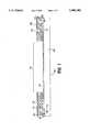
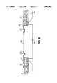
- FIG. 1shows a cross sectional view of a portion of the wafer scale multi-chip module of the present invention during fabrication after the interconnection network has been formed on the semiconductor wafer;
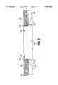
- FIG. 2shows a cross sectional view of a portion of the wafer scale multi-chip module of the present invention during fabrication after the semiconductor wafer has been etched;
- FIG. 3shows a cross sectional view of a portion of the wafer scale multi-chip module of the present invention during fabrication after the platinum has been removed to allow placement of the semiconductor chip;
- FIG. 4shows a cross sectional view of a semiconductor chip that has been etched in preparation for placement into the wafer scale multi-chip module
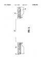
- FIG. 5shows a cross sectional view of a portion of the wafer scale multi-chip module of the present invention during fabrication after the integrated circuit die has been placed into the module and the solder has been reflowed;
- FIG. 6shows a cross sectional view of a portion of the wafer scale multi-chip module of the present invention after the bridge between the inputs and the outputs of the integrated circuit die and the interconnection network of the module have been formed;
- FIG. 7shows a cross sectional view of a portion of the wafer scale multi-chip module of the present invention with an optional heat sink attached to the back plane of the module.
- FIG. 1shows a cross sectional view of a portion of the wafer scale multi-chip module of the present invention during fabrication after the multi-layer interconnect network 110 has been formed.
- Interconnect network 110is formed by any known process. For example, ground plane 112 of platinum or platinum and copper may be sputtered onto the silicon substrate 100. Next a polyimide layer 114 of approximately 5 ⁇ m is spun onto the top surface of ground plane 112 and then patterned and etched. A chromium/copper/chromium (Cr/Cu/Cr) interconnect plane 116 of approximately 2 ⁇ m is sputtered onto the top surface of the polyimide layer 114 and then patterned and etched.
- Cr/Cu/Crchromium/copper/chromium
- the steps of the formation of polyimide and Cr/Cu/Cr layersare repeated to fabricate the number of multiple layers (114-126) of interconnections necessary for the intended circuit.
- the last layer of the interconnect network 110is polyimide layer 126, which has vias 130 formed therein for connecting interconnect network 110 to a semiconductor chip 200 (FIG. 4).
- the interconnect 110is formed in such a manner that where chips 200 are to be placed (openings 135), all interconnect layers are etched away during interconnect fabrication. Openings 135 in the interconnect 110 are just slightly larger than the size of the chip 200 plus 50 ⁇ m.
- the walls of interconnect network 110 along the openings 135are substantially vertical.
- a layer of platinumis sputtered on both the front and back sides of the silicon wafer.
- the platinum 132 on the back side of the waferis etched to serve as a mask for forming opening 136 (FIG. 2).
- a wet silicon etchantis used on the back side of wafer 100 until the ground plane 112 is reached (FIG. 2). This silicon etch will create a 45 degree slope from the top surface of the wafer module to the back surface of the wafer module, such that the back side opening is slightly wider than the front side opening.
- the openingshould also reach the edge of the interconnect network, such that the interconnect network is slightly exposed from the backside of the wafer (by approximately 25 ⁇ m) in the opening in the wafer module at 139. All exposed platinum is then removed from the wafer by means of etching, which causes opening 137 to be formed in wafer 100 (FIG. 3).
- FIG. 4shows a silicon semiconductor chip 200 that has been separated, via any conventional scribe or saw method, from a chip fabrication wafer (not shown) at perimeter 210.
- an l-shaped groove 212is etched along the top edge of chip 200.
- Groove 212is approximately 25 ⁇ m wide, is a depth X that is equal to the depth of the interconnect network 110, and extends around the entire perimeter of chip 200.
- Groove 212is etched in chip 200 in order to permit chip 200 to mate with wafer 100 at opening 135 (FIG. 1).
- the mating of chip 200 with wafer 100 in this mannerallows for a better tolerance between chip 200 and wafer 110, as etch lines can be more readily controlled than scribe lines.
- the density of chips 200 in a wafer module 100is governed by the size of the chips plus the size of the interconnect network minus 50 ⁇ m. This is to be distinguished from the prior art in which the density of a module is governed by the size of the chips plus the size of the interconnect network plus any alignment tolerance factors.l
- solder 220is flowed in groove 212 along the top edge of chip 200. While chip 200 is mated with wafer 100 at opening 135, solder 220 is reflowed (FIG. 5). This reflow procedure is done with the module upside down, which permits the chip 200 to settle and planarize itself.
- a polyimide layer 138 of approximately 5 ⁇ mis then spun onto the top surface of chip 200 and wafer 100 (FIG. 6). Polyimide layer 138 is patterned and etched to form pad openings 232 in chip 200 and pad openings 131 in wafer module 100.
- a gold layeris then spun over the top surface of chip 200 and wafer module 100. The gold layer is masked and etched to form electrical connection bridges 140 between the pad openings 232 of chip 200 and the pad openings 131 of wafer module 100.
- the present inventionhas many advantages over the prior art. For example, the mating of chip 200 to wafer module via opening 135 and groove 212 permits a tighter tolerance between the chip 200 and the wafer module 100 than conventional chip-module bonding methods. Accordingly, the method of the present invention saves acreage on wafer module 100, which allows room for more chips 200 or more interconnect 110. The present invention also permits easy removal and replacement of any bad chips by simply removing electrical connection bridges 140 and polyimide film 138 from the top of the wafer 100 and chip 200.
- the present inventionfurther permits a final wafer module that is substantially planar at both the top and bottom surfaces and substantially thinner than other multi-chip modules with a vertical height substantially equivalent to the height of a single chip 200, approximately 625 ⁇ m.
- the advantage of back planarityis that an optional heat sink 150 can be added to the back of the wafer module 100 (FIG. 7).
- Another advantage of the present inventionis that the chip 200 and the wafer 100 are comprised of substantially the same material, and therefore, have substantially the same coefficient of expansion, which helps to alleviate module, chip and interconnect damage due to uneven thermal stress.
- Another means of alleviating thermal stressis to fill openings 222 between the semiconductor chip 200 and the wafer 100 with a silicon epoxy type substance.
- the multi-chip modulecan be connected to the rest of the system via any known or later developed multi-chip module interface means. One approach anticipated by the inventor is to use the heat sink as an edge connector.
- the chip 200 and the semiconductor module 100could both be comprised of any conventional semiconductor material, such as gallium arsenide, rather than silicon.
- the interconnect network 110could consist of passive elements, such as resistors, inductors, etc., rather than just interconnect.
Landscapes
- Engineering & Computer Science (AREA)
- Computer Hardware Design (AREA)
- Microelectronics & Electronic Packaging (AREA)
- Power Engineering (AREA)
- Physics & Mathematics (AREA)
- Condensed Matter Physics & Semiconductors (AREA)
- General Physics & Mathematics (AREA)
- Cooling Or The Like Of Semiconductors Or Solid State Devices (AREA)
- Internal Circuitry In Semiconductor Integrated Circuit Devices (AREA)
- Wire Bonding (AREA)
Abstract
Description
Claims (5)
Priority Applications (1)
| Application Number | Priority Date | Filing Date | Title |
|---|---|---|---|
| US08/386,893US5506383A (en) | 1994-02-01 | 1995-02-10 | Wafer scale multi-chip module |
Applications Claiming Priority (2)
| Application Number | Priority Date | Filing Date | Title |
|---|---|---|---|
| US08/189,623US5418687A (en) | 1994-02-01 | 1994-02-01 | Wafer scale multi-chip module |
| US08/386,893US5506383A (en) | 1994-02-01 | 1995-02-10 | Wafer scale multi-chip module |
Related Parent Applications (1)
| Application Number | Title | Priority Date | Filing Date |
|---|---|---|---|
| US08/189,623DivisionUS5418687A (en) | 1994-02-01 | 1994-02-01 | Wafer scale multi-chip module |
Publications (1)
| Publication Number | Publication Date |
|---|---|
| US5506383Atrue US5506383A (en) | 1996-04-09 |
Family
ID=22698110
Family Applications (2)
| Application Number | Title | Priority Date | Filing Date |
|---|---|---|---|
| US08/189,623Expired - LifetimeUS5418687A (en) | 1994-02-01 | 1994-02-01 | Wafer scale multi-chip module |
| US08/386,893Expired - LifetimeUS5506383A (en) | 1994-02-01 | 1995-02-10 | Wafer scale multi-chip module |
Family Applications Before (1)
| Application Number | Title | Priority Date | Filing Date |
|---|---|---|---|
| US08/189,623Expired - LifetimeUS5418687A (en) | 1994-02-01 | 1994-02-01 | Wafer scale multi-chip module |
Country Status (1)
| Country | Link |
|---|---|
| US (2) | US5418687A (en) |
Cited By (17)
| Publication number | Priority date | Publication date | Assignee | Title |
|---|---|---|---|---|
| US5696666A (en)* | 1995-10-11 | 1997-12-09 | Motorola, Inc. | Low profile exposed die chip carrier package |
| US6350705B1 (en)* | 1998-08-10 | 2002-02-26 | Mecic Corporation | Wafer scale packaging scheme |
| US6413798B2 (en)* | 1998-01-18 | 2002-07-02 | Kabushiki Kaisha Toshiba | Package having very thin semiconductor chip, multichip module assembled by the package, and method for manufacturing the same |
| US6429045B1 (en) | 2001-02-07 | 2002-08-06 | International Business Machines Corporation | Structure and process for multi-chip chip attach with reduced risk of electrostatic discharge damage |
| US6510606B2 (en) | 1998-06-15 | 2003-01-28 | Lockheed Martin Corporation | Multichip module |
| US6527456B1 (en) | 1999-10-13 | 2003-03-04 | Teraconnect, Inc. | Cluster integration approach to optical transceiver arrays and fiber bundles |
| US6567963B1 (en) | 1999-10-22 | 2003-05-20 | Tera Connect, Inc. | Wafer scale integration and remoted subsystems using opto-electronic transceivers |
| US20030230801A1 (en)* | 2002-06-18 | 2003-12-18 | Tongbi Jiang | Semiconductor device assemblies and packages including multiple semiconductor devices and methods |
| US6746894B2 (en)* | 2001-03-30 | 2004-06-08 | Micron Technology, Inc. | Ball grid array interposer, packages and methods |
| US6788895B2 (en) | 1999-12-10 | 2004-09-07 | Altera Corporation | Security mapping and auto reconfiguration |
| EP1487019A1 (en)* | 2003-06-12 | 2004-12-15 | Koninklijke Philips Electronics N.V. | Electronic device and method of manufacturing thereof |
| WO2004112136A1 (en)* | 2003-06-12 | 2004-12-23 | Koninklijke Philips Electronics N.V. | Electronic device |
| US20050218518A1 (en)* | 2002-01-07 | 2005-10-06 | Tongbi Jiang | Semiconductor device assemblies and packages including multiple semiconductor device components |
| US20060043477A1 (en)* | 2002-11-11 | 2006-03-02 | Salman Akram | Interposers for chip-scale packages and intermediates thereof |
| US7271491B1 (en) | 2000-08-31 | 2007-09-18 | Micron Technology, Inc. | Carrier for wafer-scale package and wafer-scale package including the carrier |
| CN102412219A (en)* | 2010-09-22 | 2012-04-11 | 星科金朋有限公司 | Integrated circuit packaging system with active surface heat removal and method of manufacture thereof |
| US20120267775A1 (en)* | 2007-10-17 | 2012-10-25 | Neuronexus Technologies, Inc. | System and Method to Manufacture an Implantable Electrode |
Families Citing this family (12)
| Publication number | Priority date | Publication date | Assignee | Title |
|---|---|---|---|---|
| US5449427A (en)* | 1994-05-23 | 1995-09-12 | General Electric Company | Processing low dielectric constant materials for high speed electronics |
| US5723907A (en)* | 1996-06-25 | 1998-03-03 | Micron Technology, Inc. | Loc simm |
| US5811879A (en)* | 1996-06-26 | 1998-09-22 | Micron Technology, Inc. | Stacked leads-over-chip multi-chip module |
| US6250192B1 (en)* | 1996-11-12 | 2001-06-26 | Micron Technology, Inc. | Method for sawing wafers employing multiple indexing techniques for multiple die dimensions |
| US5899705A (en)* | 1997-11-20 | 1999-05-04 | Akram; Salman | Stacked leads-over chip multi-chip module |
| US6207474B1 (en) | 1998-03-09 | 2001-03-27 | Micron Technology, Inc. | Method of forming a stack of packaged memory die and resulting apparatus |
| US6815251B1 (en) | 1999-02-01 | 2004-11-09 | Micron Technology, Inc. | High density modularity for IC's |
| EP1304739A1 (en)* | 2001-10-15 | 2003-04-23 | United Test Center Inc. | Semiconductor device and method for fabricating the same |
| US10840205B2 (en) | 2017-09-24 | 2020-11-17 | Invensas Bonding Technologies, Inc. | Chemical mechanical polishing for hybrid bonding |
| US12154858B2 (en) | 2019-06-19 | 2024-11-26 | Invensas Llc | Connecting multiple chips using an interconnect device |
| US11804469B2 (en) | 2020-05-07 | 2023-10-31 | Invensas Llc | Active bridging apparatus |
| US11264357B1 (en) | 2020-10-20 | 2022-03-01 | Invensas Corporation | Mixed exposure for large die |
Citations (4)
| Publication number | Priority date | Publication date | Assignee | Title |
|---|---|---|---|---|
| US4544989A (en)* | 1980-06-30 | 1985-10-01 | Sharp Kabushiki Kaisha | Thin assembly for wiring substrate |
| US5243498A (en)* | 1992-05-26 | 1993-09-07 | Motorola, Inc. | Multi-chip semiconductor module and method for making and testing |
| US5300812A (en)* | 1992-12-09 | 1994-04-05 | General Electric Company | Plasticized polyetherimide adhesive composition and usage |
| US5313367A (en)* | 1990-06-26 | 1994-05-17 | Seiko Epson Corporation | Semiconductor device having a multilayer interconnection structure |
- 1994
- 1994-02-01USUS08/189,623patent/US5418687A/ennot_activeExpired - Lifetime
- 1995
- 1995-02-10USUS08/386,893patent/US5506383A/ennot_activeExpired - Lifetime
Patent Citations (4)
| Publication number | Priority date | Publication date | Assignee | Title |
|---|---|---|---|---|
| US4544989A (en)* | 1980-06-30 | 1985-10-01 | Sharp Kabushiki Kaisha | Thin assembly for wiring substrate |
| US5313367A (en)* | 1990-06-26 | 1994-05-17 | Seiko Epson Corporation | Semiconductor device having a multilayer interconnection structure |
| US5243498A (en)* | 1992-05-26 | 1993-09-07 | Motorola, Inc. | Multi-chip semiconductor module and method for making and testing |
| US5300812A (en)* | 1992-12-09 | 1994-04-05 | General Electric Company | Plasticized polyetherimide adhesive composition and usage |
Non-Patent Citations (40)
| Title |
|---|
| Bill Blood, "ASIC Design Methodology For Multichip Modules," Hybrid Circuit Technology, Dec. 1991, pp. 20-27. |
| Bill Blood, ASIC Design Methodology For Multichip Modules, Hybrid Circuit Technology, Dec. 1991, pp. 20 27.* |
| C. A. Neugebauer, "Comparison of VLSI Packaging Approaches To Wafer Scale Integration," Corporate Research And Development General Electric Co., Schenectady, New York, pp. 462-467. |
| C. A. Neugebauer, Comparison of VLSI Packaging Approaches To Wafer Scale Integration, Corporate Research And Development General Electric Co., Schenectady, New York, pp. 462 467.* |
| Cheng Wheling, Mark A. Beiley, and S. Simon Wong, "Membrane Multi-Chip Module Technology On Silicon," IEEE Multi-Chip Module Conference Proceedings Mar., 1993, Santa Cruz, Calif., pp. 69-73. |
| Cheng Wheling, Mark A. Beiley, and S. Simon Wong, Membrane Multi Chip Module Technology On Silicon, IEEE Multi Chip Module Conference Proceedings Mar., 1993, Santa Cruz, Calif., pp. 69 73.* |
| Clive Maxfield and Don Kuk, "A Multichip Module Primer-Does everybody understand MCMs but you?," Printed Circuit Design, Jun. 1992, pp. 17-23. |
| Clive Maxfield and Don Kuk, A Multichip Module Primer Does everybody understand MCMs but you , Printed Circuit Design, Jun. 1992, pp. 17 23.* |
| David J. Pedder, "Interconnection Technologies For Multichip Assemblies (ITMA)-A UK Information Technology Engineering Directorate Hybrid Wafer Scale Project," IEEE International Conference On Wafer Scale Integration, San Francisco, Calif., 1993, pp. 95-107. |
| David J. Pedder, Interconnection Technologies For Multichip Assemblies ( ITMA ) A UK Information Technology Engineering Directorate Hybrid Wafer Scale Project, IEEE International Conference On Wafer Scale Integration, San Francisco, Calif., 1993, pp. 95 107.* |
| Dr. Alastair Trigg, "Silicon Hybrid Multichip Modules," Hybrid Circuit Technology, May 1991, pp. 44-50. |
| Dr. Alastair Trigg, Silicon Hybrid Multichip Modules, Hybrid Circuit Technology, May 1991, pp. 44 50.* |
| Gail Lehman Lamer, Douglas B. Hoy and Kathy M. Middo, New Multilayer Polyimide Technology Teams With Multilayer Ceramics To Form MultiChip Modules Hybrid Circuit Technology , Oct. 1990, pp. 21 26.* |
| Gail Lehman-Lamer, Douglas B. Hoy and Kathy M. Middo, "New Multilayer Polyimide Technology Teams With Multilayer Ceramics To Form MultiChip Modules Hybrid Circuit Technology", Oct. 1990, pp. 21-26. |
| Harry F. Lockwood, "Hybrid Wafer Scale Optoelectronic Integration," SPIE vol. 1389-International Conference on Advances In Interconnection And Packaging, 1990, pp. 55--67. |
| Harry F. Lockwood, Hybrid Wafer Scale Optoelectronic Integration, SPIE vol. 1389 International Conference on Advances In Interconnection And Packaging, 1990, pp. 55 67.* |
| Howard W. Markstein, "Multichip Modules Pursue Wafer Scale Perforamnce," Electronic Packaging & Production, Oct. 1994, pp. 40-45. |
| Howard W. Markstein, Multichip Modules Pursue Wafer Scale Perforamnce, Electronic Packaging & Production, Oct. 1994, pp. 40 45.* |
| Hyman J. Levinstein, Charles J. Bartlett and Walter J. Bertram, Jr., "Multi-Chip Packaging Technology For VLSI-Based Systems," and Clinton C. Chao, Kenneth D. Scholz, Jacques Leibovitz, Maria Cobarruviaz and Cheng C. Cheng, "Multi-Layer Thin-Film Substrates For Multi-Chip Packaing," IEEE Log Number 8927118, Dec. 1988, pp. 472-478. |
| Hyman J. Levinstein, Charles J. Bartlett and Walter J. Bertram, Jr., Multi Chip Packaging Technology For VLSI Based Systems, and Clinton C. Chao, Kenneth D. Scholz, Jacques Leibovitz, Maria Cobarruviaz and Cheng C. Cheng, Multi Layer Thin Film Substrates For Multi Chip Packaing, IEEE Log Number 8927118, Dec. 1988, pp. 472 478.* |
| John K. Hagge, "Ultro-Reliable Packaging for Silicon-On-Silicon WSI," IEEE Transactions On Components, Hybrids, And Manufacturing Technology, vol. 12, No. 2, Jun. 1989, pp. 170-179. |
| John K. Hagge, Ultro Reliable Packaging for Silicon On Silicon WSI, IEEE Transactions On Components, Hybrids, And Manufacturing Technology, vol. 12, No. 2, Jun. 1989, pp. 170 179.* |
| Krishna Shenai, "Part VIII Multichip Packaging And Metallization Reliability and Albert J. Blodgett, Jr., Microelectronic Packaging," pp. 449-461. |
| Krishna Shenai, Part VIII Multichip Packaging And Metallization Reliability and Albert J. Blodgett, Jr., Microelectronic Packaging, pp. 449 461.* |
| L. M. Levinson, C. W. Eichelberger, R. J. Wojnarowski, and R. O. Carlson, "High-Density Interconnects Using Laser Lithography," ISHM, 1988 Proceedings pp. 301-306. |
| L. M. Levinson, C. W. Eichelberger, R. J. Wojnarowski, and R. O. Carlson, High Density Interconnects Using Laser Lithography, ISHM, 1988 Proceedings pp. 301 306.* |
| M. Burnus, H. Taddiken, H. D. Hartmann, and T. Hillmann Ruge, Laserpersonalization Of Interconnection Arrays For Hybride ASIC s, IEEE International Conference On Wafer Scale Integration, 1993, San Francisco, Calif., 329 339.* |
| M. Burnus, H. Taddiken, H.-D. Hartmann, and T. Hillmann-Ruge, "Laserpersonalization Of Interconnection Arrays For Hybride ASIC's," IEEE International Conference On Wafer Scale Integration, 1993, San Francisco, Calif., 329-339. |
| M. G. Sage, "Multichip Modules--The Hybrid for Wafer-Scale Integration," Hybrid Circuits, No. 21, Jan. 1990, pp. 36-38. |
| M. G. Sage, Multichip Modules The Hybrid for Wafer Scale Integration, Hybrid Circuits, No. 21, Jan. 1990, pp. 36 38.* |
| Paul D. Franzon and Rober J. Evans, "A Multichip Module Design Process For Notebook Computers," IEEE Proceedings, Apr. 1993, pp. 41-49. |
| Paul D. Franzon and Rober J. Evans, A Multichip Module Design Process For Notebook Computers, IEEE Proceedings, Apr. 1993, pp. 41 49.* |
| Ron Iscoff, "Are MCMs The New Packaging Champ?," Semiconductor International, Dec. 1992, pp. 48-55. |
| Ron Iscoff, Are MCMs The New Packaging Champ , Semiconductor International, Dec. 1992, pp. 48 55.* |
| Scott Westbrook, "Test Vehicle For MCM-D Interconnect Process Development," IEEE Multi-Chip Module Conference, Santa Cruz, Calif., Mar., 1993 pp. 106-110. |
| Scott Westbrook, Test Vehicle For MCM D Interconnect Process Development, IEEE Multi Chip Module Conference, Santa Cruz, Calif., Mar., 1993 pp. 106 110.* |
| Terry Costlow, "Two Join MCM Market," Electronic Engineering Times, Jun. 7, 1993, p. 58. |
| Terry Costlow, Two Join MCM Market, Electronic Engineering Times, Jun. 7, 1993, p. 58.* |
| Wolfgang Daum, William E. Burdick Jr., and Raymond A. Fillion, "Overlay High-Density Interconnect: A Chips-First Multichip Module Technology," IEEE Proceedings, Apr. 1993, pp. 23-29. |
| Wolfgang Daum, William E. Burdick Jr., and Raymond A. Fillion, Overlay High Density Interconnect: A Chips First Multichip Module Technology, IEEE Proceedings, Apr. 1993, pp. 23 29.* |
Cited By (32)
| Publication number | Priority date | Publication date | Assignee | Title |
|---|---|---|---|---|
| US5696666A (en)* | 1995-10-11 | 1997-12-09 | Motorola, Inc. | Low profile exposed die chip carrier package |
| US6413798B2 (en)* | 1998-01-18 | 2002-07-02 | Kabushiki Kaisha Toshiba | Package having very thin semiconductor chip, multichip module assembled by the package, and method for manufacturing the same |
| US6510606B2 (en) | 1998-06-15 | 2003-01-28 | Lockheed Martin Corporation | Multichip module |
| US6350705B1 (en)* | 1998-08-10 | 2002-02-26 | Mecic Corporation | Wafer scale packaging scheme |
| US6527456B1 (en) | 1999-10-13 | 2003-03-04 | Teraconnect, Inc. | Cluster integration approach to optical transceiver arrays and fiber bundles |
| US6567963B1 (en) | 1999-10-22 | 2003-05-20 | Tera Connect, Inc. | Wafer scale integration and remoted subsystems using opto-electronic transceivers |
| US6788895B2 (en) | 1999-12-10 | 2004-09-07 | Altera Corporation | Security mapping and auto reconfiguration |
| US7271491B1 (en) | 2000-08-31 | 2007-09-18 | Micron Technology, Inc. | Carrier for wafer-scale package and wafer-scale package including the carrier |
| US7517797B2 (en) | 2000-08-31 | 2009-04-14 | Micron Technology, Inc. | Carrier for wafer-scale package, wafer-scale package including the carrier, and methods |
| US6429045B1 (en) | 2001-02-07 | 2002-08-06 | International Business Machines Corporation | Structure and process for multi-chip chip attach with reduced risk of electrostatic discharge damage |
| US6746894B2 (en)* | 2001-03-30 | 2004-06-08 | Micron Technology, Inc. | Ball grid array interposer, packages and methods |
| US20040217459A1 (en)* | 2001-03-30 | 2004-11-04 | Fee Setho Sing | Ball grid array interposer, packages and methods |
| US7528007B2 (en) | 2001-03-30 | 2009-05-05 | Micron Technology, Inc. | Methods for assembling semiconductor devices and interposers |
| US7274095B2 (en)* | 2001-03-30 | 2007-09-25 | Micron Technology, Inc. | Interposers with receptacles for receiving semiconductor devices and assemblies and packages including such interposers |
| US20050218518A1 (en)* | 2002-01-07 | 2005-10-06 | Tongbi Jiang | Semiconductor device assemblies and packages including multiple semiconductor device components |
| US20030230801A1 (en)* | 2002-06-18 | 2003-12-18 | Tongbi Jiang | Semiconductor device assemblies and packages including multiple semiconductor devices and methods |
| US20040106229A1 (en)* | 2002-06-27 | 2004-06-03 | Tongbi Jiang | Methods for assembling multiple semiconductor devices |
| US6906415B2 (en) | 2002-06-27 | 2005-06-14 | Micron Technology, Inc. | Semiconductor device assemblies and packages including multiple semiconductor devices and methods |
| US7573136B2 (en) | 2002-06-27 | 2009-08-11 | Micron Technology, Inc. | Semiconductor device assemblies and packages including multiple semiconductor device components |
| US7198980B2 (en) | 2002-06-27 | 2007-04-03 | Micron Technology, Inc. | Methods for assembling multiple semiconductor devices |
| US7368812B2 (en) | 2002-11-11 | 2008-05-06 | Micron Technology, Inc. | Interposers for chip-scale packages and intermediates thereof |
| US20060043477A1 (en)* | 2002-11-11 | 2006-03-02 | Salman Akram | Interposers for chip-scale packages and intermediates thereof |
| WO2004112136A1 (en)* | 2003-06-12 | 2004-12-23 | Koninklijke Philips Electronics N.V. | Electronic device |
| JP2006527499A (en)* | 2003-06-12 | 2006-11-30 | コーニンクレッカ フィリップス エレクトロニクス エヌ ヴィ | Package for high frequency electronic equipment |
| US7098530B2 (en) | 2003-06-12 | 2006-08-29 | Koninklijke Philips Electronics, N.V. | Package for a high-frequency electronic device |
| WO2004112134A1 (en)* | 2003-06-12 | 2004-12-23 | Koninklijke Philips Electronics N.V. | Package for a high-frequency electronic device |
| EP1487019A1 (en)* | 2003-06-12 | 2004-12-15 | Koninklijke Philips Electronics N.V. | Electronic device and method of manufacturing thereof |
| US20060131736A1 (en)* | 2003-06-12 | 2006-06-22 | Jansman Andreas B M | Package for a high-frequency electronic device |
| US20120267775A1 (en)* | 2007-10-17 | 2012-10-25 | Neuronexus Technologies, Inc. | System and Method to Manufacture an Implantable Electrode |
| US8658465B2 (en)* | 2007-10-17 | 2014-02-25 | Neuronexus Technologies, Inc. | System and method to manufacture an implantable electrode |
| US8703537B2 (en)* | 2007-10-17 | 2014-04-22 | Neuronexus Technologies, Inc. | System and method to manufacture an implantable electrode |
| CN102412219A (en)* | 2010-09-22 | 2012-04-11 | 星科金朋有限公司 | Integrated circuit packaging system with active surface heat removal and method of manufacture thereof |
Also Published As
| Publication number | Publication date |
|---|---|
| US5418687A (en) | 1995-05-23 |
Similar Documents
| Publication | Publication Date | Title |
|---|---|---|
| US5506383A (en) | Wafer scale multi-chip module | |
| CN112514062B (en) | Multi-chip package structure with chip interconnect bridges providing power connection between chips and package substrate | |
| US7517778B2 (en) | Structure of high performance combo chip and processing method | |
| US5611140A (en) | Method of forming electrically conductive polymer interconnects on electrical substrates | |
| US5222014A (en) | Three-dimensional multi-chip pad array carrier | |
| US4628406A (en) | Method of packaging integrated circuit chips, and integrated circuit package | |
| US6294407B1 (en) | Microelectronic packages including thin film decal and dielectric adhesive layer having conductive vias therein, and methods of fabricating the same | |
| US7230334B2 (en) | Semiconductor integrated circuit chip packages having integrated microchannel cooling modules | |
| US7348261B2 (en) | Wafer scale thin film package | |
| US12199080B2 (en) | Electronics card including multi-chip module | |
| US20090140404A1 (en) | Hermetic seal and reliable bonding structures for 3d applications | |
| HK1004352B (en) | Stackable three-dimensional multiple chip semiconductor device and method for making the same | |
| US8153516B2 (en) | Method of ball grid array package construction with raised solder ball pads | |
| US5367765A (en) | Method of fabricating integrated circuit chip package | |
| US5151388A (en) | Flip interconnect | |
| JPH07170098A (en) | Mounting structure of electronic parts and mounting method | |
| TW202412120A (en) | Three-dimensional packaging structure and its preparation method thereof | |
| EP0475223B1 (en) | Method of fabricating integrated circuit chip package | |
| US6571468B1 (en) | Traceless flip chip assembly and method | |
| WO1995005675A1 (en) | Method of forming electrically conductive polymer interconnects on electrical substrates | |
| JP3735986B2 (en) | Multichip module and manufacturing method thereof |
Legal Events
| Date | Code | Title | Description |
|---|---|---|---|
| STCF | Information on status: patent grant | Free format text:PATENTED CASE | |
| FEPP | Fee payment procedure | Free format text:PAYOR NUMBER ASSIGNED (ORIGINAL EVENT CODE: ASPN); ENTITY STATUS OF PATENT OWNER: LARGE ENTITY | |
| FPAY | Fee payment | Year of fee payment:4 | |
| AS | Assignment | Owner name:HEWLETT-PACKARD COMPANY, A DELAWARE CORPORATION, C Free format text:MERGER;ASSIGNOR:HEWLETT-PACKARD COMPANY, A CALIFORNIA CORPORATION;REEL/FRAME:010841/0649 Effective date:19980520 | |
| AS | Assignment | Owner name:AGILENT TECHNOLOGIES INC, CALIFORNIA Free format text:ASSIGNMENT OF ASSIGNORS INTEREST;ASSIGNOR:HEWLETT-PACKARD COMPANY;REEL/FRAME:010977/0540 Effective date:19991101 | |
| FPAY | Fee payment | Year of fee payment:8 | |
| AS | Assignment | Owner name:AVAGO TECHNOLOGIES GENERAL IP PTE. LTD., SINGAPORE Free format text:ASSIGNMENT OF ASSIGNORS INTEREST;ASSIGNOR:AGILENT TECHNOLOGIES, INC.;REEL/FRAME:017207/0020 Effective date:20051201 | |
| AS | Assignment | Owner name:CITICORP NORTH AMERICA, INC.,DELAWARE Free format text:SECURITY AGREEMENT;ASSIGNOR:AVAGO TECHNOLOGIES GENERAL IP (SINGAPORE) PTE. LTD.;REEL/FRAME:017207/0882 Effective date:20051201 Owner name:CITICORP NORTH AMERICA, INC., DELAWARE Free format text:SECURITY AGREEMENT;ASSIGNOR:AVAGO TECHNOLOGIES GENERAL IP (SINGAPORE) PTE. LTD.;REEL/FRAME:017207/0882 Effective date:20051201 | |
| FPAY | Fee payment | Year of fee payment:12 | |
| AS | Assignment | Owner name:AVAGO TECHNOLOGIES GENERAL IP (SINGAPORE) PTE. LTD Free format text:RELEASE BY SECURED PARTY;ASSIGNOR:CITICORP NORTH AMERICA, INC.;REEL/FRAME:030420/0048 Effective date:20110331 | |
| AS | Assignment | Owner name:AVAGO TECHNOLOGIES GENERAL IP (SINGAPORE) PTE. LTD Free format text:CORRECTIVE ASSIGNMENT TO CORRECT THE NAME OF THE ASSIGNEE PREVIOUSLY RECORDED ON REEL 017207 FRAME 0020. ASSIGNOR(S) HEREBY CONFIRMS THE ASSIGNMENT;ASSIGNOR:AGILENT TECHNOLOGIES, INC.;REEL/FRAME:038633/0001 Effective date:20051201 |