US5501993A - Method of constructing CMOS vertically modulated wells (VMW) by clustered MeV BILLI (buried implanted layer for lateral isolation) implantation - Google Patents
Method of constructing CMOS vertically modulated wells (VMW) by clustered MeV BILLI (buried implanted layer for lateral isolation) implantationDownload PDFInfo
- Publication number
- US5501993A US5501993AUS08/343,116US34311694AUS5501993AUS 5501993 AUS5501993 AUS 5501993AUS 34311694 AUS34311694 AUS 34311694AUS 5501993 AUS5501993 AUS 5501993A
- Authority
- US
- United States
- Prior art keywords
- energy
- sufficient
- well
- mask
- retrograde
- Prior art date
- Legal status (The legal status is an assumption and is not a legal conclusion. Google has not performed a legal analysis and makes no representation as to the accuracy of the status listed.)
- Expired - Fee Related
Links
Images


Classifications
- H—ELECTRICITY
- H01—ELECTRIC ELEMENTS
- H01L—SEMICONDUCTOR DEVICES NOT COVERED BY CLASS H10
- H01L21/00—Processes or apparatus adapted for the manufacture or treatment of semiconductor or solid state devices or of parts thereof
- H01L21/70—Manufacture or treatment of devices consisting of a plurality of solid state components formed in or on a common substrate or of parts thereof; Manufacture of integrated circuit devices or of parts thereof
- H01L21/71—Manufacture of specific parts of devices defined in group H01L21/70
- H01L21/76—Making of isolation regions between components
- H01L21/762—Dielectric regions, e.g. EPIC dielectric isolation, LOCOS; Trench refilling techniques, SOI technology, use of channel stoppers
- H01L21/76202—Dielectric regions, e.g. EPIC dielectric isolation, LOCOS; Trench refilling techniques, SOI technology, use of channel stoppers using a local oxidation of silicon, e.g. LOCOS, SWAMI, SILO
- H01L21/76213—Dielectric regions, e.g. EPIC dielectric isolation, LOCOS; Trench refilling techniques, SOI technology, use of channel stoppers using a local oxidation of silicon, e.g. LOCOS, SWAMI, SILO introducing electrical inactive or active impurities in the local oxidation region, e.g. to alter LOCOS oxide growth characteristics or for additional isolation purpose
- H01L21/76216—Dielectric regions, e.g. EPIC dielectric isolation, LOCOS; Trench refilling techniques, SOI technology, use of channel stoppers using a local oxidation of silicon, e.g. LOCOS, SWAMI, SILO introducing electrical inactive or active impurities in the local oxidation region, e.g. to alter LOCOS oxide growth characteristics or for additional isolation purpose introducing electrical active impurities in the local oxidation region for the sole purpose of creating channel stoppers
- H01L21/76218—Dielectric regions, e.g. EPIC dielectric isolation, LOCOS; Trench refilling techniques, SOI technology, use of channel stoppers using a local oxidation of silicon, e.g. LOCOS, SWAMI, SILO introducing electrical inactive or active impurities in the local oxidation region, e.g. to alter LOCOS oxide growth characteristics or for additional isolation purpose introducing electrical active impurities in the local oxidation region for the sole purpose of creating channel stoppers introducing both types of electrical active impurities in the local oxidation region for the sole purpose of creating channel stoppers, e.g. for isolation of complementary doped regions
- H—ELECTRICITY
- H10—SEMICONDUCTOR DEVICES; ELECTRIC SOLID-STATE DEVICES NOT OTHERWISE PROVIDED FOR
- H10D—INORGANIC ELECTRIC SEMICONDUCTOR DEVICES
- H10D84/00—Integrated devices formed in or on semiconductor substrates that comprise only semiconducting layers, e.g. on Si wafers or on GaAs-on-Si wafers
- H10D84/01—Manufacture or treatment
- H10D84/0123—Integrating together multiple components covered by H10D12/00 or H10D30/00, e.g. integrating multiple IGBTs
- H10D84/0126—Integrating together multiple components covered by H10D12/00 or H10D30/00, e.g. integrating multiple IGBTs the components including insulated gates, e.g. IGFETs
- H10D84/0165—Integrating together multiple components covered by H10D12/00 or H10D30/00, e.g. integrating multiple IGBTs the components including insulated gates, e.g. IGFETs the components including complementary IGFETs, e.g. CMOS devices
- H—ELECTRICITY
- H01—ELECTRIC ELEMENTS
- H01L—SEMICONDUCTOR DEVICES NOT COVERED BY CLASS H10
- H01L21/00—Processes or apparatus adapted for the manufacture or treatment of semiconductor or solid state devices or of parts thereof
- H01L21/70—Manufacture or treatment of devices consisting of a plurality of solid state components formed in or on a common substrate or of parts thereof; Manufacture of integrated circuit devices or of parts thereof
- H01L21/71—Manufacture of specific parts of devices defined in group H01L21/70
- H01L21/76—Making of isolation regions between components
- H01L21/761—PN junctions
- H—ELECTRICITY
- H10—SEMICONDUCTOR DEVICES; ELECTRIC SOLID-STATE DEVICES NOT OTHERWISE PROVIDED FOR
- H10D—INORGANIC ELECTRIC SEMICONDUCTOR DEVICES
- H10D84/00—Integrated devices formed in or on semiconductor substrates that comprise only semiconducting layers, e.g. on Si wafers or on GaAs-on-Si wafers
- H10D84/01—Manufacture or treatment
- H10D84/0123—Integrating together multiple components covered by H10D12/00 or H10D30/00, e.g. integrating multiple IGBTs
- H10D84/0126—Integrating together multiple components covered by H10D12/00 or H10D30/00, e.g. integrating multiple IGBTs the components including insulated gates, e.g. IGFETs
- H10D84/0165—Integrating together multiple components covered by H10D12/00 or H10D30/00, e.g. integrating multiple IGBTs the components including insulated gates, e.g. IGFETs the components including complementary IGFETs, e.g. CMOS devices
- H10D84/0191—Manufacturing their doped wells
- H—ELECTRICITY
- H10—SEMICONDUCTOR DEVICES; ELECTRIC SOLID-STATE DEVICES NOT OTHERWISE PROVIDED FOR
- H10D—INORGANIC ELECTRIC SEMICONDUCTOR DEVICES
- H10D84/00—Integrated devices formed in or on semiconductor substrates that comprise only semiconducting layers, e.g. on Si wafers or on GaAs-on-Si wafers
- H10D84/01—Manufacture or treatment
- H10D84/02—Manufacture or treatment characterised by using material-based technologies
- H10D84/03—Manufacture or treatment characterised by using material-based technologies using Group IV technology, e.g. silicon technology or silicon-carbide [SiC] technology
- H10D84/038—Manufacture or treatment characterised by using material-based technologies using Group IV technology, e.g. silicon technology or silicon-carbide [SiC] technology using silicon technology, e.g. SiGe
- H—ELECTRICITY
- H10—SEMICONDUCTOR DEVICES; ELECTRIC SOLID-STATE DEVICES NOT OTHERWISE PROVIDED FOR
- H10D—INORGANIC ELECTRIC SEMICONDUCTOR DEVICES
- H10D84/00—Integrated devices formed in or on semiconductor substrates that comprise only semiconducting layers, e.g. on Si wafers or on GaAs-on-Si wafers
- H10D84/80—Integrated devices formed in or on semiconductor substrates that comprise only semiconducting layers, e.g. on Si wafers or on GaAs-on-Si wafers characterised by the integration of at least one component covered by groups H10D12/00 or H10D30/00, e.g. integration of IGFETs
- H10D84/82—Integrated devices formed in or on semiconductor substrates that comprise only semiconducting layers, e.g. on Si wafers or on GaAs-on-Si wafers characterised by the integration of at least one component covered by groups H10D12/00 or H10D30/00, e.g. integration of IGFETs of only field-effect components
- H10D84/83—Integrated devices formed in or on semiconductor substrates that comprise only semiconducting layers, e.g. on Si wafers or on GaAs-on-Si wafers characterised by the integration of at least one component covered by groups H10D12/00 or H10D30/00, e.g. integration of IGFETs of only field-effect components of only insulated-gate FETs [IGFET]
- H10D84/85—Complementary IGFETs, e.g. CMOS
- H10D84/856—Complementary IGFETs, e.g. CMOS the complementary IGFETs having different architectures than each other, e.g. high-voltage and low-voltage CMOS
Definitions
- the present inventionrelates to simplification of a manufacturing process for complementary semiconductor devices, which are becoming increasingly miniaturized and increasingly complex, to a high component-density semiconductor device having enhanced resistance to CMOS latch-up, and to well formation (single, twin, triple).
- CMOS technologyin the VSLI field has grown, as a result of requirements for a high noise margin and low power consumption.
- miniaturizationhas increased, serious problems have arisen with regard to preventing stray thyristor operation which causes the CMOS latch-up phenomenon to occur between mutually adjacent portions of an n-channel MOSFET and p-channel MOSFET, and with regard to maintaining a sufficient level of withstanding voltage between mutually adjacent elements.
- the present inventionsolves the following problems:
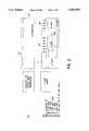
- FIG. 1is a schematic view of a BILLI structure in accordance with the invention.
- Jig. 2is a schematic view of the steps involved in manufacturing a BILLI twin-well structure with two masks and clustered implantation;
- FIG. 3is a schematic view of the steps involved in manufacturing a BILLI triple-well structure with two masks and clustered implantation;
- FIG. 4is a schematic view showing an alternative process to that of FIG. 3;
- FIG. 5is a schematic view showing another alternative process to that of FIG. 3.
- FIG. 1shows a low cost MeV structure in accordance with the invention at the stage in its manufacture at which PMOS devices can be formed in a retrograde n-well and NMOS devices in a retrograde p-well.
- PMOS devicesare shown, in order to indicate where they will be formed in steps subsequent to said stage.
- Isolation areas 5separate adjacent PMOS devices which can be implanted into a retrograde n-well formed in a p-type substrate 10.
- the retrograde n-wellincludes an upper layer 6 wherein phosphorus ions have been implanted so as to form phosphorus (n) impurity atoms with a density that is produced by 5E12cm-2! and a lower layer 7 wherein phosphorus ions have been implanted so as to form phosphorus (n) impurity atoms with a density that is produced by 3E13cm-2.
- the retrograde p-wellincludes an upper layer 8 wherein boron ions have been implanted so as to form boron (p) impurity atoms with a density that is produced by 5E12cm-2! and a lower layer 9 wherein boron ions have been implanted so as to form boron (p) impurity atoms with a density that is produced by 3E13cm-2.
- the term "upper layer”signifies the layer which is nearer the active surface of the substrate 10 and is 0.5 ⁇ m deep.
- the term “lower layer”signifies the layer which is farther from the active surface of the substrate 10 and is 1.2 ⁇ m deep.
- the BILLI structureis formed by continuance of the boron layers from the depths at which they are formed beneath a thick masking layer, for example: comprising at least 2 ⁇ m of photoresist to the depths at which they are formed in the absence of the thick masking layer.
- the latter depthsare under the retrograde n-well, deeper than both the upper layer 6 and the lower layer 7, and the layers at these depths are designated "buried”.
- the boron layers at these depthsthus form a "buried implanted layer for lateral isolation" or "BILLI” structure, since they surround the n-well around the sides and the bottom.
- This BILLI structureprovides best latch-up resistance for miminum n+ to p+ spacing even over epi-wafers. When combined with hydrogen denudation, this BILLI structure on bulk Cz wafers can lead to epi replacement.
- FIG. 2, in conjunction with FIG. 1,shows a method of forming the BILLI structure in accordance with the invention.
- This method of the inventionnot only has the advantage of resulting in the formation of the novel BILLI structure of the invention, but also results in both process simplification and cost reducton for single, twin and triple well formation.
- a preferred embodiment of the method of the inventioncomprehends the following steps. First, isolation areas 12 are formed (or, alternatively, active areas are formed) in the substrate 10. Then a mask 11, such as a photoresist mask having a thickness of more than 2.0 ⁇ m is placed on the surface as shown to block the phosphorus ions of maximum energy, and a clustered series of four to six implants are carried out.
- a mask 11such as a photoresist mask having a thickness of more than 2.0 ⁇ m is placed on the surface as shown to block the phosphorus ions of maximum energy, and a clustered series of four to six implants are carried out.
- the clustered series of four to six implantsmay be carried out as follows: First, boron ions are directed onto the upper surface of the substrate 10 with an energy of 2.00 MeV, thereby forming the lower layer 9 of p-type material (deep retrograde p-well). Second, without removing the substrate 10 from the vacuum chamber in which it was irradiated with boron ions, the parameters of the ion accelerator are changed, and boron ions are directed onto the upper surface of the substrate 10 with an energy of 1.25 MeV, thereby forming the upper layer 8 of p-type material (channel stop implant or shallow retrograde p-well).
- the parameters of the ion acceleratorare changed, and boron ions are directed onto the upper surface of the substrate 10 with an energy of 750 keV, thereby forming a shallow, thin threshhold voltage layer V t at the surface of the retrograde p-well 8,9.
- the parameters of the ion acceleratorare changed, and phosphorus ions are directed onto the upper surface of the substrate 10 with an energy of 1 MeV, thereby forming the lower layer 7 of n-type material (deep retrograde n-well).
- the parameters of the ion acceleratorare changed, and phosphorus ions are directed onto the upper surface of the substrate 10 with an energy of 450 keV, thereby forming the upper layer 6 of n-type material (channel stop implant or shallow retrograde n-well).
- the sixth stepwithout removing the substrate 10 from the vacuum chamber in which it was irradiated with boron ions and phosphorus ions, the parameters of the ion accelerator are changed, and phosphorus ions are directed onto the upper surface of the substrate 10 with an energy of 60 keV, thereby forming a shallow, thin threshhold voltage layer V t at the surface of the retrograde n-well 6,7.
- the sixth stepmay comprise directing boron ions onto the upper surface of the substrate 10 with an energy of 30 keV so as to form this threshhold voltage layer.
- the method of FIG. 2may be modified by omitting the two optional steps and, in lieu thereof, carrying out a medium current blanket Vt implant after the M1 step and before the M2 step.
- the sixth stepmay be omitted and, in lieu thereof, a medium current blanket Vt implant may be carried out after the M1 step and before the M2 step.
- a BILLI triple well structureis formed.
- a BILLI triple well structuremay be formed by the clustered implantation indicated in FIG. 4, wherein the implantation steps are carried out on a p-type substrate in the following sequence.
- phosphorus ionsare directed onto the upper surface of the substrate 110 with an energy of 3.0 MeV, thereby forming the lower layer 109 of n-type material.
- the parameters of the ion acceleratorare changed, and phosphorus ions are directed onto the upper surface of the substrate 110 with an energy of 2.25 MeV, thereby forming the upper layer 108 of n-type material.
- the parameters of the ion acceleratorare changed, and phosphorus ions are directed onto the upper surface of the substrate 110 with an energy of 2.0 MeV, thereby forming a shallow, thin threshhold voltage layer V t at the surface of the retrograde n-well 108,109.
- the parameters of the ion acceleratorare changed, and boron ions are directed onto the upper surface of the substrate 110 with an energy of 500 keV, thereby forming the lower layer 107 of p-type material.
- the parameters of the ion acceleratorare changed, and boron ions are directed onto the upper surface of the substrate 110 with an energy of 250 keV, thereby forming the upper layer 106 of p-type material.
- the parameters of the ion acceleratorare changed, and boron ions are directed onto the upper surface of the substrate 110 with an energy of 30 keV, thereby forming a shallow, thin threshhold voltage layer V t at the surface of the retrograde p-well 106,107.
- a BILLI triple well structuremay be formed by the clustered implantation indicated in FIG. 5, wherein the bottom ("buried") n-layer is formed prior to the clustered implant steps by a separate implantation of 3.0 MeV phosphorus ions at a current of 3 to 5 E13 through a separate mask, designated "M2" in FIG. 5. The remaining, clustered implantation steps are carried out through a separate mask, designated "M3" in FIG. 5, in the following sequence.
- boron ionsare directed onto the upper surface of the substrate 110 with an energy of 2.0 MeV and a dose of 0.5 to 1 E13, thereby forming the lower layer 107 of p-type material in the p-wells.
- the parameters of the ion acceleratorare changed, and boron ions are directed onto the upper surface of the substrate 110 with an energy of 1.25 MeV, thereby forming the upper layer 106 of p-type material in the p-wells.
- the parameters of the ion acceleratorare changed, and boron ions are directed onto the upper surface of the substrate 110 with an energy of 750 keV, thereby forming a shallow, thin threshhold voltage layer V t at the surface of the retrograde p-well 106,107.
- the parameters of the ion acceleratorare changed, and phosphorus ions are directed onto the upper surface of the substrate 110 with an energy of 1.0 MeV, thereby forming the lower layer 109 of n-type material.
- the parameters of the ion acceleratorare changed, and phosphorus ions are directed onto the upper surface of the substrate 110 with an energy of 450 keV, thereby forming the upper layer 108 of n-type material.
- the sixth stepwithout removing the substrate 110 from the vacuum chamber in which it was irradiated with boron ions and phosphorus ions, the parameters of the ion accelerator are changed, and boron ions are directed onto the upper surface of the substrate 110 with an energy of 30 keV, thereby forming a shallow, thin threshhold voltage layer V t at the surface of the retrograde n-well 106,107.
- the sixth stepmay comprise directing phosphorus ions onto the upper surface of the substrate 110 with an energy of 60 keV so as to form this threshhold voltage layer.
- sequence of clustered implantionsare carried out by the same ion accelerator.
- sequence of clustered implantationsmay be carried out by separate ion accelerators without departing from the spirit and scope of the invention; it is only necessary to ensure that the same mask is used throughout the sequence of clustered implantations.
- representative thicknesses of the masksare set forth, and representative energies of the ions being implanted are set forth.
- the inventionis not limited to such thicknesses or energies, and the invention comprehends, in general, phosphorus-ion energies which are insufficient to pass through the mask involved, thus being blocked by the mask, and boron-ion energies which are sufficient to pass through the mask involved.
- the inventionhas been described in terms of boron ions and phosphorus ions.
- the inventionincludes the use of p-type dopants other than boron in lieu of boron ions, as well as the use of n-type dopants other than phosphorus in lieu of phosphorus ions.
Landscapes
- Engineering & Computer Science (AREA)
- Physics & Mathematics (AREA)
- Condensed Matter Physics & Semiconductors (AREA)
- General Physics & Mathematics (AREA)
- Manufacturing & Machinery (AREA)
- Computer Hardware Design (AREA)
- Microelectronics & Electronic Packaging (AREA)
- Power Engineering (AREA)
- Metal-Oxide And Bipolar Metal-Oxide Semiconductor Integrated Circuits (AREA)
- Element Separation (AREA)
Abstract
Description
Claims (21)
Priority Applications (6)
| Application Number | Priority Date | Filing Date | Title |
|---|---|---|---|
| US08/343,116US5501993A (en) | 1994-11-22 | 1994-11-22 | Method of constructing CMOS vertically modulated wells (VMW) by clustered MeV BILLI (buried implanted layer for lateral isolation) implantation |
| EP95939891AEP0793858A4 (en) | 1994-11-22 | 1995-11-09 | CONSTRUCTING CMOS VERTICALLY MODULATED WELLS BY CLUSTERED MeV BURIED IMPLANTED LAYER FOR LATERAL ISOLATION |
| JP8516937AJPH10509281A (en) | 1994-11-22 | 1995-11-09 | Method of Constructing a CMOS Vertical Adjustment Well (VMW) by Implanting Clustered MEV BILLI |
| PCT/US1995/014653WO1996016439A1 (en) | 1994-11-22 | 1995-11-09 | CONSTRUCTING CMOS VERTICALLY MODULATED WELLS BY CLUSTERED MeV BURIED IMPLANTED LAYER FOR LATERAL ISOLATION |
| KR1019970703421AKR100272394B1 (en) | 1994-11-22 | 1995-11-09 | Method of constructing cmos vertically modulatrd wells by clustered mev billi implantion |
| US08/617,293US5814866A (en) | 1994-11-22 | 1996-03-18 | Semiconductor device having at least one field oxide area and CMOS vertically modulated wells (VMW) with a buried implanted layer for lateral isolation having a first portion below a well, a second portion forming another, adjacent well, and a vertical po |
Applications Claiming Priority (1)
| Application Number | Priority Date | Filing Date | Title |
|---|---|---|---|
| US08/343,116US5501993A (en) | 1994-11-22 | 1994-11-22 | Method of constructing CMOS vertically modulated wells (VMW) by clustered MeV BILLI (buried implanted layer for lateral isolation) implantation |
Related Child Applications (1)
| Application Number | Title | Priority Date | Filing Date |
|---|---|---|---|
| US08/617,293Continuation-In-PartUS5814866A (en) | 1994-11-22 | 1996-03-18 | Semiconductor device having at least one field oxide area and CMOS vertically modulated wells (VMW) with a buried implanted layer for lateral isolation having a first portion below a well, a second portion forming another, adjacent well, and a vertical po |
Publications (1)
| Publication Number | Publication Date |
|---|---|
| US5501993Atrue US5501993A (en) | 1996-03-26 |
Family
ID=23344782
Family Applications (2)
| Application Number | Title | Priority Date | Filing Date |
|---|---|---|---|
| US08/343,116Expired - Fee RelatedUS5501993A (en) | 1994-11-22 | 1994-11-22 | Method of constructing CMOS vertically modulated wells (VMW) by clustered MeV BILLI (buried implanted layer for lateral isolation) implantation |
| US08/617,293Expired - LifetimeUS5814866A (en) | 1994-11-22 | 1996-03-18 | Semiconductor device having at least one field oxide area and CMOS vertically modulated wells (VMW) with a buried implanted layer for lateral isolation having a first portion below a well, a second portion forming another, adjacent well, and a vertical po |
Family Applications After (1)
| Application Number | Title | Priority Date | Filing Date |
|---|---|---|---|
| US08/617,293Expired - LifetimeUS5814866A (en) | 1994-11-22 | 1996-03-18 | Semiconductor device having at least one field oxide area and CMOS vertically modulated wells (VMW) with a buried implanted layer for lateral isolation having a first portion below a well, a second portion forming another, adjacent well, and a vertical po |
Country Status (5)
| Country | Link |
|---|---|
| US (2) | US5501993A (en) |
| EP (1) | EP0793858A4 (en) |
| JP (1) | JPH10509281A (en) |
| KR (1) | KR100272394B1 (en) |
| WO (1) | WO1996016439A1 (en) |
Cited By (52)
| Publication number | Priority date | Publication date | Assignee | Title |
|---|---|---|---|---|
| US5573963A (en)* | 1995-05-03 | 1996-11-12 | Vanguard International Semiconductor Corporation | Method of forming self-aligned twin tub CMOS devices |
| US5573962A (en)* | 1995-12-15 | 1996-11-12 | Vanguard International Semiconductor Corporation | Low cycle time CMOS process |
| US5693505A (en)* | 1993-12-24 | 1997-12-02 | Nec Corporation | Method of fabricating a semiconductor device |
| EP0831518A1 (en)* | 1996-09-05 | 1998-03-25 | Matsushita Electronics Corporation | Semiconductor device and method for producing the same |
| US5753956A (en)* | 1996-01-11 | 1998-05-19 | Micron Technology, Inc. | Semiconductor processing methods of forming complementary metal oxide semiconductor memory and other circuitry, and memory and other circuitry |
| US5759884A (en)* | 1996-10-30 | 1998-06-02 | Lg Semicon Co., Ltd. | Method for forming well of semiconductor device |
| GB2320812A (en)* | 1996-12-30 | 1998-07-01 | Hyundai Electronics Ind | Method for forming a triple well of a semiconductor device |
| US5795803A (en)* | 1996-08-29 | 1998-08-18 | Sharp Kabushiki Kaisha | Method for manufacturing a semiconductor device |
| KR19980060631A (en)* | 1996-12-31 | 1998-10-07 | 김영환 | Manufacturing method of semiconductor device |
| US5821589A (en)* | 1997-03-19 | 1998-10-13 | Genus, Inc. | Method for cmos latch-up improvement by mev billi (buried implanted layer for laternal isolation) plus buried layer implantation |
| US5831313A (en)* | 1996-08-15 | 1998-11-03 | Integrated Device Technology, Inc. | Structure for improving latch-up immunity and interwell isolation in a semiconductor device |
| US5858826A (en)* | 1996-01-16 | 1999-01-12 | United Microelectronics Corporation | Method of making a blanket N-well structure for SRAM data stability in P-type substrates |
| US5858828A (en)* | 1997-02-18 | 1999-01-12 | Symbios, Inc. | Use of MEV implantation to form vertically modulated N+ buried layer in an NPN bipolar transistor |
| US5877051A (en)* | 1997-08-22 | 1999-03-02 | Micron Technology, Inc. | Methods of reducing alpha particle inflicted damage to SRAM cells, methods of forming integrated circuitry, and methods of forming SRAM cells |
| US5880515A (en)* | 1996-09-30 | 1999-03-09 | Lsi Logic Corporation | Circuit isolation utilizing MeV implantation |
| US5895251A (en)* | 1996-05-02 | 1999-04-20 | Lg Semicon Co., Ltd | Method for forming a triple-well in a semiconductor device |
| EP0809296A3 (en)* | 1996-05-21 | 1999-05-06 | LSI Logic Corporation | Method of fabricating a semiconductor device with protection means |
| US5927991A (en)* | 1995-12-30 | 1999-07-27 | Lg Semicon Co., Ltd. | Method for forming triple well in semiconductor device |
| US5963798A (en)* | 1996-06-29 | 1999-10-05 | Hyundai Electronics Industries Co., Ltd. | Fabrication method of CMOS device having buried implanted layers for lateral isolation (BILLI) |
| US5972745A (en)* | 1997-05-30 | 1999-10-26 | International Business Machines Corporation | Method or forming self-aligned halo-isolated wells |
| US5985743A (en)* | 1996-09-19 | 1999-11-16 | Advanced Micro Devices, Inc. | Single mask substrate doping process for CMOS integrated circuits |
| US6017785A (en)* | 1996-08-15 | 2000-01-25 | Integrated Device Technology, Inc. | Method for improving latch-up immunity and interwell isolation in a semiconductor device |
| US6020614A (en)* | 1998-03-25 | 2000-02-01 | Worley; Eugene Robert | Method of reducing substrate noise coupling in mixed signal integrated circuits |
| US6066523A (en)* | 1997-06-30 | 2000-05-23 | Hyundai Electronics Industries Co., Ltd. | Method for fabricating a semiconductor device having triple wells |
| US6069048A (en)* | 1998-09-30 | 2000-05-30 | Lsi Logic Corporation | Reduction of silicon defect induced failures as a result of implants in CMOS and other integrated circuits |
| US6096611A (en)* | 1998-03-13 | 2000-08-01 | Texas Instruments - Acer Incorporated | Method to fabricate dual threshold CMOS circuits |
| US6107672A (en)* | 1997-09-04 | 2000-08-22 | Matsushita Electronics Corporation | Semiconductor device having a plurality of buried wells |
| US6187643B1 (en) | 1999-06-29 | 2001-02-13 | Varian Semiconductor Equipment Associates, Inc. | Simplified semiconductor device manufacturing using low energy high tilt angle and high energy post-gate ion implantation (PoGI) |
| US6251744B1 (en) | 1999-07-19 | 2001-06-26 | Taiwan Semiconductor Manufacturing Company | Implant method to improve characteristics of high voltage isolation and high voltage breakdown |
| US6268248B1 (en)* | 1997-12-23 | 2001-07-31 | Texas Instruments Incorporated | Method of fabricating a source line in flash memory having STI structures |
| KR100322889B1 (en)* | 1999-12-30 | 2002-02-09 | 박종섭 | Method for manufacturing a semiconductor device |
| GB2365625A (en)* | 1996-12-30 | 2002-02-20 | Hyundai Electronics Ind | Method for forming a triple well of a semiconductor device |
| US6362035B1 (en) | 2000-02-07 | 2002-03-26 | Taiwan Semiconductor Manufacturing Company | Channel stop ion implantation method for CMOS integrated circuits |
| US6376336B1 (en) | 2001-02-01 | 2002-04-23 | Advanced Micro Devices, Inc. | Frontside SOI gettering with phosphorus doping |
| US6444534B1 (en) | 2001-01-30 | 2002-09-03 | Advanced Micro Devices, Inc. | SOI semiconductor device opening implantation gettering method |
| US6503783B1 (en)* | 2000-08-31 | 2003-01-07 | Micron Technology, Inc. | SOI CMOS device with reduced DIBL |
| US6670259B1 (en) | 2001-02-21 | 2003-12-30 | Advanced Micro Devices, Inc. | Inert atom implantation method for SOI gettering |
| US20040097057A1 (en)* | 2002-11-19 | 2004-05-20 | Silterra Malaysia Sdn. Bhd. | Method of forming ultra shallow junctions |
| US20040259318A1 (en)* | 2002-09-29 | 2004-12-23 | Advanced Analogic Technologies, Inc. | Modular bipolar-CMOS-DMOS analog integrated circuit and power transistor technology |
| US20050014329A1 (en)* | 2002-08-14 | 2005-01-20 | Advanced Analogic Technologies, Inc. | Method of fabricating isolated semiconductor devices in epi-less substrate |
| US6872640B1 (en) | 2004-03-16 | 2005-03-29 | Micron Technology, Inc. | SOI CMOS device with reduced DIBL |
| US6885078B2 (en)* | 2001-11-09 | 2005-04-26 | Lsi Logic Corporation | Circuit isolation utilizing MeV implantation |
| US20050179093A1 (en)* | 2004-02-17 | 2005-08-18 | Silicon Space Technology Corporation | Buried guard ring and radiation hardened isolation structures and fabrication methods |
| US6958264B1 (en) | 2001-04-03 | 2005-10-25 | Advanced Micro Devices, Inc. | Scribe lane for gettering of contaminants on SOI wafers and gettering method |
| US7009250B1 (en) | 2004-08-20 | 2006-03-07 | Micron Technology, Inc. | FinFET device with reduced DIBL |
| KR100479814B1 (en)* | 1997-03-24 | 2006-05-22 | 주식회사 하이닉스반도체 | Well Forming Method of Semiconductor Device |
| US20070141794A1 (en)* | 2005-10-14 | 2007-06-21 | Silicon Space Technology Corporation | Radiation hardened isolation structures and fabrication methods |
| US20070206424A1 (en)* | 2006-03-06 | 2007-09-06 | Powerchip Semiconductor Corp. | Method for erasing non-volatile memory |
| US20080142899A1 (en)* | 2006-08-04 | 2008-06-19 | Silicon Space Technology Corporation | Radiation immunity of integrated circuits using backside die contact and electrically conductive layers |
| US9257504B2 (en) | 2002-09-29 | 2016-02-09 | Advanced Analogic Technologies Incorporated | Isolation structures for semiconductor devices |
| US10038058B2 (en) | 2016-05-07 | 2018-07-31 | Silicon Space Technology Corporation | FinFET device structure and method for forming same |
| CN111082093A (en)* | 2019-12-27 | 2020-04-28 | 武汉理工大学 | Hydrogen fuel cell stack durability test system and method |
Families Citing this family (21)
| Publication number | Priority date | Publication date | Assignee | Title |
|---|---|---|---|---|
| JP3394408B2 (en)* | 1997-01-13 | 2003-04-07 | 株式会社リコー | Semiconductor device and manufacturing method thereof |
| US6133077A (en) | 1998-01-13 | 2000-10-17 | Lsi Logic Corporation | Formation of high-voltage and low-voltage devices on a semiconductor substrate |
| KR100282706B1 (en)* | 1998-07-07 | 2001-03-02 | 윤종용 | Manufacturing Method of Semiconductor Device |
| JP2000091443A (en)* | 1998-09-14 | 2000-03-31 | Mitsubishi Electric Corp | Semiconductor device and method of manufacturing the same |
| JP3733252B2 (en)* | 1998-11-02 | 2006-01-11 | セイコーエプソン株式会社 | Semiconductor memory device and manufacturing method thereof |
| KR100324931B1 (en) | 1999-01-22 | 2002-02-28 | 박종섭 | Method of Fabricating a Twin Well CMOS Device |
| US6063672A (en)* | 1999-02-05 | 2000-05-16 | Lsi Logic Corporation | NMOS electrostatic discharge protection device and method for CMOS integrated circuit |
| US6268250B1 (en) | 1999-05-14 | 2001-07-31 | Micron Technology, Inc. | Efficient fabrication process for dual well type structures |
| US6445014B1 (en) | 1999-06-16 | 2002-09-03 | Micron Technology Inc. | Retrograde well structure for a CMOS imager |
| US6310366B1 (en) | 1999-06-16 | 2001-10-30 | Micron Technology, Inc. | Retrograde well structure for a CMOS imager |
| EP1096575A1 (en)* | 1999-10-07 | 2001-05-02 | STMicroelectronics S.r.l. | Non-volatile memory cell with a single level of polysilicon and corresponding manufacturing process |
| EP1091408A1 (en) | 1999-10-07 | 2001-04-11 | STMicroelectronics S.r.l. | Non-volatile memory cell with a single level of polysilicon |
| US6406974B1 (en)* | 2000-03-24 | 2002-06-18 | United Microelectronics Corp. | Method of forming triple N well utilizing phosphorus and boron ion implantations |
| JP2002043557A (en)* | 2000-07-21 | 2002-02-08 | Mitsubishi Electric Corp | Semiconductor device having solid-state imaging device and method of manufacturing the same |
| US6610585B1 (en)* | 2002-02-26 | 2003-08-26 | International Business Machines Corporation | Method for forming a retrograde implant |
| US6667205B2 (en) | 2002-04-19 | 2003-12-23 | International Business Machines Machines Corporation | Method of forming retrograde n-well and p-well |
| US6949802B2 (en)* | 2003-11-20 | 2005-09-27 | Taiwan Semiconductor Manufacturing Co., Ltd. | ESD protection structure |
| US7442996B2 (en)* | 2006-01-20 | 2008-10-28 | International Business Machines Corporation | Structure and method for enhanced triple well latchup robustness |
| US7662690B2 (en)* | 2006-01-31 | 2010-02-16 | Texas Instruments Incorporated | Method of preparing a semiconductor substrate utilizing plural implants under an isolation region to isolate adjacent wells |
| US20100009527A1 (en)* | 2008-07-14 | 2010-01-14 | Chartered Semiconductor Manufacturing Ltd. | Integrated circuit system employing single mask layer technique for well formation |
| DE102013018789B4 (en) | 2012-11-29 | 2025-03-06 | Infineon Technologies Ag | Controlling light-generated charge carriers |
Citations (3)
| Publication number | Priority date | Publication date | Assignee | Title |
|---|---|---|---|---|
| US4710477A (en)* | 1983-09-12 | 1987-12-01 | Hughes Aircraft Company | Method for forming latch-up immune, multiple retrograde well high density CMOS FET |
| US5160996A (en)* | 1987-10-08 | 1992-11-03 | Matsushita Electric Industrial Co., Inc. | Structure and method of manufacture for semiconductor device |
| US5384279A (en)* | 1988-09-09 | 1995-01-24 | U.S. Philips Corporation | Method of manufacturing a semiconductor device comprising a silicon body in which semiconductor regions are formed by ion implantations |
Family Cites Families (5)
| Publication number | Priority date | Publication date | Assignee | Title |
|---|---|---|---|---|
| US5292671A (en)* | 1987-10-08 | 1994-03-08 | Matsushita Electric Industrial, Co., Ltd. | Method of manufacture for semiconductor device by forming deep and shallow regions |
| JPH02305468A (en)* | 1989-05-19 | 1990-12-19 | Mitsubishi Electric Corp | Manufacture of semiconductor device |
| JP2965783B2 (en)* | 1991-07-17 | 1999-10-18 | 三菱電機株式会社 | Semiconductor device and manufacturing method thereof |
| JP2978345B2 (en)* | 1992-11-26 | 1999-11-15 | 三菱電機株式会社 | Method for manufacturing semiconductor device |
| JP2682425B2 (en)* | 1993-12-24 | 1997-11-26 | 日本電気株式会社 | Method for manufacturing semiconductor device |
- 1994
- 1994-11-22USUS08/343,116patent/US5501993A/ennot_activeExpired - Fee Related
- 1995
- 1995-11-09EPEP95939891Apatent/EP0793858A4/ennot_activeWithdrawn
- 1995-11-09JPJP8516937Apatent/JPH10509281A/enactivePending
- 1995-11-09KRKR1019970703421Apatent/KR100272394B1/ennot_activeExpired - Fee Related
- 1995-11-09WOPCT/US1995/014653patent/WO1996016439A1/ennot_activeApplication Discontinuation
- 1996
- 1996-03-18USUS08/617,293patent/US5814866A/ennot_activeExpired - Lifetime
Patent Citations (3)
| Publication number | Priority date | Publication date | Assignee | Title |
|---|---|---|---|---|
| US4710477A (en)* | 1983-09-12 | 1987-12-01 | Hughes Aircraft Company | Method for forming latch-up immune, multiple retrograde well high density CMOS FET |
| US5160996A (en)* | 1987-10-08 | 1992-11-03 | Matsushita Electric Industrial Co., Inc. | Structure and method of manufacture for semiconductor device |
| US5384279A (en)* | 1988-09-09 | 1995-01-24 | U.S. Philips Corporation | Method of manufacturing a semiconductor device comprising a silicon body in which semiconductor regions are formed by ion implantations |
Non-Patent Citations (4)
| Title |
|---|
| Diffusion/Implantation, Dec. 1993 "MeV Implantation Technology Next-generation manufacturing with current-generation equipment" John Ogawa Borland, Ron Koelsch. brochure pp. 1-8. |
| Diffusion/Implantation, Dec. 1993 MeV Implantation Technology Next generation manufacturing with current generation equipment John Ogawa Borland, Ron Koelsch. brochure pp. 1 8.* |
| Fowler, "MosFet Devices with high-gate dielectric integrity", IBM TDB, vol. 17, No. 1, Jun. 1974. |
| Fowler, MosFet Devices with high gate dielectric integrity , IBM TDB, vol. 17, No. 1, Jun. 1974.* |
Cited By (102)
| Publication number | Priority date | Publication date | Assignee | Title |
|---|---|---|---|---|
| US5693505A (en)* | 1993-12-24 | 1997-12-02 | Nec Corporation | Method of fabricating a semiconductor device |
| US5573963A (en)* | 1995-05-03 | 1996-11-12 | Vanguard International Semiconductor Corporation | Method of forming self-aligned twin tub CMOS devices |
| US5573962A (en)* | 1995-12-15 | 1996-11-12 | Vanguard International Semiconductor Corporation | Low cycle time CMOS process |
| US5927991A (en)* | 1995-12-30 | 1999-07-27 | Lg Semicon Co., Ltd. | Method for forming triple well in semiconductor device |
| US5753956A (en)* | 1996-01-11 | 1998-05-19 | Micron Technology, Inc. | Semiconductor processing methods of forming complementary metal oxide semiconductor memory and other circuitry, and memory and other circuitry |
| US5950079A (en)* | 1996-01-11 | 1999-09-07 | Micron Technology, Inc. | Semiconductor processing methods of forming complementary metal oxide semiconductor memory and other circuitry |
| US6064098A (en)* | 1996-01-11 | 2000-05-16 | Micron Technology, Inc. | Semiconductor processing methods of forming complementary metal oxide semiconductor memory and other circuitry, and memory and other circuitry |
| US5858826A (en)* | 1996-01-16 | 1999-01-12 | United Microelectronics Corporation | Method of making a blanket N-well structure for SRAM data stability in P-type substrates |
| US5895251A (en)* | 1996-05-02 | 1999-04-20 | Lg Semicon Co., Ltd | Method for forming a triple-well in a semiconductor device |
| EP0809296A3 (en)* | 1996-05-21 | 1999-05-06 | LSI Logic Corporation | Method of fabricating a semiconductor device with protection means |
| US5963798A (en)* | 1996-06-29 | 1999-10-05 | Hyundai Electronics Industries Co., Ltd. | Fabrication method of CMOS device having buried implanted layers for lateral isolation (BILLI) |
| US5831313A (en)* | 1996-08-15 | 1998-11-03 | Integrated Device Technology, Inc. | Structure for improving latch-up immunity and interwell isolation in a semiconductor device |
| US6017785A (en)* | 1996-08-15 | 2000-01-25 | Integrated Device Technology, Inc. | Method for improving latch-up immunity and interwell isolation in a semiconductor device |
| US5795803A (en)* | 1996-08-29 | 1998-08-18 | Sharp Kabushiki Kaisha | Method for manufacturing a semiconductor device |
| US6066522A (en)* | 1996-09-05 | 2000-05-23 | Matsushita Electronics Corporation | Semiconductor device and method for producing the same |
| EP0831518A1 (en)* | 1996-09-05 | 1998-03-25 | Matsushita Electronics Corporation | Semiconductor device and method for producing the same |
| US5985743A (en)* | 1996-09-19 | 1999-11-16 | Advanced Micro Devices, Inc. | Single mask substrate doping process for CMOS integrated circuits |
| US5880515A (en)* | 1996-09-30 | 1999-03-09 | Lsi Logic Corporation | Circuit isolation utilizing MeV implantation |
| US6319793B1 (en) | 1996-09-30 | 2001-11-20 | Lsi Logic Corporation | Circuit isolation utilizing MeV implantation |
| CN1097310C (en)* | 1996-10-30 | 2002-12-25 | Lg半导体株式会社 | Method of forming well of semiconductor device |
| US5759884A (en)* | 1996-10-30 | 1998-06-02 | Lg Semicon Co., Ltd. | Method for forming well of semiconductor device |
| GB2320812B (en)* | 1996-12-30 | 2002-01-09 | Hyundai Electronics Ind | Method for forming a triple well of a semiconductor device |
| GB2320812A (en)* | 1996-12-30 | 1998-07-01 | Hyundai Electronics Ind | Method for forming a triple well of a semiconductor device |
| GB2365625A (en)* | 1996-12-30 | 2002-02-20 | Hyundai Electronics Ind | Method for forming a triple well of a semiconductor device |
| US6010926A (en)* | 1996-12-30 | 2000-01-04 | Hyundai Electronics Industries Co., Ltd. | Method for forming multiple or modulated wells of semiconductor device |
| GB2365625B (en)* | 1996-12-30 | 2002-05-15 | Hyundai Electronics Ind | Method for forming a triple well of a semiconductor device |
| KR19980060631A (en)* | 1996-12-31 | 1998-10-07 | 김영환 | Manufacturing method of semiconductor device |
| US5858828A (en)* | 1997-02-18 | 1999-01-12 | Symbios, Inc. | Use of MEV implantation to form vertically modulated N+ buried layer in an NPN bipolar transistor |
| US6316817B1 (en) | 1997-02-18 | 2001-11-13 | Lsi Logic Corporation | MeV implantation to form vertically modulated N+ buried layer in an NPN bipolar transistor |
| EP0912998A4 (en)* | 1997-03-19 | 2005-04-20 | Varian Semiconductor Equipment | Method for cmos latch-up improvement by mev billi (buried implanted layer for lateral isolation) plus buried layer implantation |
| US5821589A (en)* | 1997-03-19 | 1998-10-13 | Genus, Inc. | Method for cmos latch-up improvement by mev billi (buried implanted layer for laternal isolation) plus buried layer implantation |
| KR100479814B1 (en)* | 1997-03-24 | 2006-05-22 | 주식회사 하이닉스반도체 | Well Forming Method of Semiconductor Device |
| US5972745A (en)* | 1997-05-30 | 1999-10-26 | International Business Machines Corporation | Method or forming self-aligned halo-isolated wells |
| US6066523A (en)* | 1997-06-30 | 2000-05-23 | Hyundai Electronics Industries Co., Ltd. | Method for fabricating a semiconductor device having triple wells |
| US6146936A (en)* | 1997-08-22 | 2000-11-14 | Micron Technology, Inc. | Integrated circuitry, methods of reducing alpha particle inflicted damage to SRAM cells, methods of forming integrated circuitry, and methods of forming SRAM cells |
| US5877051A (en)* | 1997-08-22 | 1999-03-02 | Micron Technology, Inc. | Methods of reducing alpha particle inflicted damage to SRAM cells, methods of forming integrated circuitry, and methods of forming SRAM cells |
| US6107672A (en)* | 1997-09-04 | 2000-08-22 | Matsushita Electronics Corporation | Semiconductor device having a plurality of buried wells |
| US6268248B1 (en)* | 1997-12-23 | 2001-07-31 | Texas Instruments Incorporated | Method of fabricating a source line in flash memory having STI structures |
| US6096611A (en)* | 1998-03-13 | 2000-08-01 | Texas Instruments - Acer Incorporated | Method to fabricate dual threshold CMOS circuits |
| US6020614A (en)* | 1998-03-25 | 2000-02-01 | Worley; Eugene Robert | Method of reducing substrate noise coupling in mixed signal integrated circuits |
| US6069048A (en)* | 1998-09-30 | 2000-05-30 | Lsi Logic Corporation | Reduction of silicon defect induced failures as a result of implants in CMOS and other integrated circuits |
| WO2001001449A3 (en)* | 1999-06-29 | 2001-07-05 | Varian Semiconductor Equipment | Semiconductor device manufacturing using low energy high tilt angle ion implantation |
| US6187643B1 (en) | 1999-06-29 | 2001-02-13 | Varian Semiconductor Equipment Associates, Inc. | Simplified semiconductor device manufacturing using low energy high tilt angle and high energy post-gate ion implantation (PoGI) |
| US6251744B1 (en) | 1999-07-19 | 2001-06-26 | Taiwan Semiconductor Manufacturing Company | Implant method to improve characteristics of high voltage isolation and high voltage breakdown |
| KR100322889B1 (en)* | 1999-12-30 | 2002-02-09 | 박종섭 | Method for manufacturing a semiconductor device |
| US6362035B1 (en) | 2000-02-07 | 2002-03-26 | Taiwan Semiconductor Manufacturing Company | Channel stop ion implantation method for CMOS integrated circuits |
| US6716682B1 (en) | 2000-08-31 | 2004-04-06 | Micron Technology, Inc. | SOI CMOS device with reduced DIBL |
| US6503783B1 (en)* | 2000-08-31 | 2003-01-07 | Micron Technology, Inc. | SOI CMOS device with reduced DIBL |
| US20070026652A1 (en)* | 2000-08-31 | 2007-02-01 | Mouli Chandra V | SOI device with reduced drain induced barrier lowering |
| US7122411B2 (en) | 2000-08-31 | 2006-10-17 | Micron Technology, Inc | SOI device with reduced drain induced barrier lowering |
| US7566600B2 (en) | 2000-08-31 | 2009-07-28 | Micron Technology, Inc. | SOI device with reduced drain induced barrier lowering |
| US6635928B2 (en) | 2000-08-31 | 2003-10-21 | Micron Technology, Inc. | SOI CMOS device with reduced DIBL |
| US20050020041A1 (en)* | 2000-08-31 | 2005-01-27 | Mouli Chandra V. | SOI device with reduced drain induced barrier lowering |
| US6905918B2 (en) | 2000-08-31 | 2005-06-14 | Micron Technology, Inc. | SOI device with reduced drain induced barrier lowering |
| US6444534B1 (en) | 2001-01-30 | 2002-09-03 | Advanced Micro Devices, Inc. | SOI semiconductor device opening implantation gettering method |
| US6376336B1 (en) | 2001-02-01 | 2002-04-23 | Advanced Micro Devices, Inc. | Frontside SOI gettering with phosphorus doping |
| US6670259B1 (en) | 2001-02-21 | 2003-12-30 | Advanced Micro Devices, Inc. | Inert atom implantation method for SOI gettering |
| US6958264B1 (en) | 2001-04-03 | 2005-10-25 | Advanced Micro Devices, Inc. | Scribe lane for gettering of contaminants on SOI wafers and gettering method |
| US6885078B2 (en)* | 2001-11-09 | 2005-04-26 | Lsi Logic Corporation | Circuit isolation utilizing MeV implantation |
| US20050142792A1 (en)* | 2002-08-14 | 2005-06-30 | Advanced Analogic Technologies, Inc. | Method of fabricating isolated semiconductor devices in epi-less substrate |
| US7449380B2 (en) | 2002-08-14 | 2008-11-11 | Advanced Analogic Technologies, Inc. | Method of fabricating isolated semiconductor devices in epi-less substrate |
| US20050014324A1 (en)* | 2002-08-14 | 2005-01-20 | Advanced Analogic Technologies, Inc. | Method of fabricating isolated semiconductor devices in epi-less substrate |
| US20050142791A1 (en)* | 2002-08-14 | 2005-06-30 | Advanced Analogic Technologies, Inc. | Method of fabricating isolated semiconductor devices in epi-less substrate |
| US20050142724A1 (en)* | 2002-08-14 | 2005-06-30 | Advanced Analogic Technologies, Inc. | Method of fabricating isolated semiconductor devices in epi-less substrate |
| US20050158939A1 (en)* | 2002-08-14 | 2005-07-21 | Advanced Analogic Technologies, Inc | Method of fabricating isolated semiconductor devices in epi-less substrate |
| US7666756B2 (en)* | 2002-08-14 | 2010-02-23 | Advanced Analogic Technologies, Inc. | Methods of fabricating isolation structures in epi-less substrate |
| US20050014329A1 (en)* | 2002-08-14 | 2005-01-20 | Advanced Analogic Technologies, Inc. | Method of fabricating isolated semiconductor devices in epi-less substrate |
| US7279378B2 (en)* | 2002-08-14 | 2007-10-09 | Advanced Analogic Technologies, Inc. | Method of fabricating isolated semiconductor devices in epi-less substrate |
| US7329583B2 (en) | 2002-08-14 | 2008-02-12 | Advanced Analogic Technologies, Inc. | Method of fabricating isolated semiconductor devices in epi-less substrate |
| US7276431B2 (en) | 2002-08-14 | 2007-10-02 | Advanced Analogic Technologies, Inc. | Method of fabricating isolated semiconductor devices in epi-less substrate |
| US7422938B2 (en) | 2002-08-14 | 2008-09-09 | Advanced Analogic Technologies, Inc. | Method of fabricating isolated semiconductor devices in epi-less substrate |
| US9905640B2 (en) | 2002-09-29 | 2018-02-27 | Skyworks Solutions (Hong Kong) Limited | Isolation structures for semiconductor devices including trenches containing conductive material |
| US10074716B2 (en) | 2002-09-29 | 2018-09-11 | Skyworks Solutions (Hong Kong) Limited | Saucer-shaped isolation structures for semiconductor devices |
| US9257504B2 (en) | 2002-09-29 | 2016-02-09 | Advanced Analogic Technologies Incorporated | Isolation structures for semiconductor devices |
| US20040259318A1 (en)* | 2002-09-29 | 2004-12-23 | Advanced Analogic Technologies, Inc. | Modular bipolar-CMOS-DMOS analog integrated circuit and power transistor technology |
| US7279399B2 (en)* | 2002-09-29 | 2007-10-09 | Advanced Analogic Technologies, Inc. | Method of forming isolated pocket in a semiconductor substrate |
| US20040097057A1 (en)* | 2002-11-19 | 2004-05-20 | Silterra Malaysia Sdn. Bhd. | Method of forming ultra shallow junctions |
| US20040224488A1 (en)* | 2002-11-19 | 2004-11-11 | Silterra Malaysia Sdn. Bhd. | Method of forming ultra shallow junctions |
| US6767809B2 (en)* | 2002-11-19 | 2004-07-27 | Silterra Malayisa Sdn. Bhd. | Method of forming ultra shallow junctions |
| US7804138B2 (en) | 2004-02-17 | 2010-09-28 | Silicon Space Technology Corp. | Buried guard ring and radiation hardened isolation structures and fabrication methods |
| US8729640B2 (en) | 2004-02-17 | 2014-05-20 | Silicon Space Technology Corporation | Method and structure for radiation hardening a semiconductor device |
| US20080073725A1 (en)* | 2004-02-17 | 2008-03-27 | Morris Wesley H | Buried guard ring structures and fabrication methods |
| US7304354B2 (en) | 2004-02-17 | 2007-12-04 | Silicon Space Technology Corp. | Buried guard ring and radiation hardened isolation structures and fabrication methods |
| US20080188045A1 (en)* | 2004-02-17 | 2008-08-07 | Morris Wesley H | Methods for operating and fabricating a semiconductor device having a buried guard ring structure |
| US20060249759A1 (en)* | 2004-02-17 | 2006-11-09 | Morris Wesley H | Buried guard ring and radiation hardened isolation structures and fabrication methods |
| US8497195B2 (en) | 2004-02-17 | 2013-07-30 | Silicon Space Technology Corporation | Method for radiation hardening a semiconductor device |
| US8093145B2 (en) | 2004-02-17 | 2012-01-10 | Silicon Space Technology Corp. | Methods for operating and fabricating a semiconductor device having a buried guard ring structure |
| US7629654B2 (en) | 2004-02-17 | 2009-12-08 | Silicon Space Technology Corp. | Buried guard ring structures and fabrication methods |
| US20050179093A1 (en)* | 2004-02-17 | 2005-08-18 | Silicon Space Technology Corporation | Buried guard ring and radiation hardened isolation structures and fabrication methods |
| US20050205931A1 (en)* | 2004-03-16 | 2005-09-22 | Mouli Chandra V | SOI CMOS device with reduced DIBL |
| US6872640B1 (en) | 2004-03-16 | 2005-03-29 | Micron Technology, Inc. | SOI CMOS device with reduced DIBL |
| US7235468B1 (en) | 2004-08-20 | 2007-06-26 | Micron Technology, Inc. | FinFET device with reduced DIBL |
| US7009250B1 (en) | 2004-08-20 | 2006-03-07 | Micron Technology, Inc. | FinFET device with reduced DIBL |
| US20100267212A1 (en)* | 2005-10-14 | 2010-10-21 | Morris Wesley H | Fabrication methods for radiation hardened isolation structures |
| US8252642B2 (en) | 2005-10-14 | 2012-08-28 | Silicon Space Technology Corp. | Fabrication methods for radiation hardened isolation structures |
| US8278719B2 (en) | 2005-10-14 | 2012-10-02 | Silicon Space Technology Corp. | Radiation hardened isolation structures and fabrication methods |
| US20070141794A1 (en)* | 2005-10-14 | 2007-06-21 | Silicon Space Technology Corporation | Radiation hardened isolation structures and fabrication methods |
| US20070206424A1 (en)* | 2006-03-06 | 2007-09-06 | Powerchip Semiconductor Corp. | Method for erasing non-volatile memory |
| US20080142899A1 (en)* | 2006-08-04 | 2008-06-19 | Silicon Space Technology Corporation | Radiation immunity of integrated circuits using backside die contact and electrically conductive layers |
| US10615260B1 (en) | 2016-05-07 | 2020-04-07 | Silicon Space Technology Corporation | Method for forming FinFET device structure |
| US10038058B2 (en) | 2016-05-07 | 2018-07-31 | Silicon Space Technology Corporation | FinFET device structure and method for forming same |
| CN111082093A (en)* | 2019-12-27 | 2020-04-28 | 武汉理工大学 | Hydrogen fuel cell stack durability test system and method |
Also Published As
| Publication number | Publication date |
|---|---|
| US5814866A (en) | 1998-09-29 |
| EP0793858A1 (en) | 1997-09-10 |
| EP0793858A4 (en) | 1998-08-19 |
| JPH10509281A (en) | 1998-09-08 |
| KR980700687A (en) | 1998-03-30 |
| KR100272394B1 (en) | 2000-12-01 |
| WO1996016439A1 (en) | 1996-05-30 |
Similar Documents
| Publication | Publication Date | Title |
|---|---|---|
| US5501993A (en) | Method of constructing CMOS vertically modulated wells (VMW) by clustered MeV BILLI (buried implanted layer for lateral isolation) implantation | |
| US4435895A (en) | Process for forming complementary integrated circuit devices | |
| CA1257710A (en) | Method for the manufacture of lsi complementary mos field effect transistor circuits | |
| US4662061A (en) | Method for fabricating a CMOS well structure | |
| EP0139019A1 (en) | Semiconductor device and method of manufacture thereof | |
| US6514833B1 (en) | Method of inhibiting lateral diffusion between adjacent wells by introducing carbon or fluorine ions into bottom of STI groove | |
| JP3031880B2 (en) | Semiconductor device and manufacturing method thereof | |
| US7524710B2 (en) | Radiation-hardened silicon-on-insulator CMOS device, and method of making the same | |
| US6342438B2 (en) | Method of manufacturing a dual doped CMOS gate | |
| KR100324931B1 (en) | Method of Fabricating a Twin Well CMOS Device | |
| US5821589A (en) | Method for cmos latch-up improvement by mev billi (buried implanted layer for laternal isolation) plus buried layer implantation | |
| CA1223975A (en) | Process for making a semiconductor device | |
| JPS63278265A (en) | Manufacturing method of semiconductor BiCMOS device | |
| JPS5932163A (en) | CMOS integrated circuit | |
| JPH1055976A (en) | Method of manufacturing semiconductor device having various buried regions | |
| US6291327B1 (en) | Optimization of S/D annealing to minimize S/D shorts in memory array | |
| JPH08227936A (en) | Semiconductor device and fabrication thereof | |
| KR100564262B1 (en) | Method for improving CMOS latch-up by MEV BILLI and buried layer injection | |
| JP3035915B2 (en) | Semiconductor device and manufacturing method thereof | |
| JPH09223747A (en) | Method for manufacturing semiconductor device | |
| JPS61127147A (en) | semiconductor equipment | |
| KR100223582B1 (en) | Method for manufacturing semiconductor device with SIMOX structure | |
| JP3057692B2 (en) | Method for manufacturing semiconductor device | |
| EP0762493A1 (en) | Semiconductor device having field oxide regions and a field implant and method of manufacturing the same | |
| KR950014113B1 (en) | Manufacturing Method of Semiconductor Device |
Legal Events
| Date | Code | Title | Description |
|---|---|---|---|
| AS | Assignment | Owner name:GENUS, INC., CALIFORNIA Free format text:ASSIGNMENT OF ASSIGNORS INTEREST;ASSIGNOR:BORLAND, JOHN O.;REEL/FRAME:007229/0067 Effective date:19941118 | |
| AS | Assignment | Owner name:SUMITOMO BANK OF CALIFORNIA, CALIFORNIA Free format text:SECURITY AGREEMENT;ASSIGNOR:GENUS, INC.;REEL/FRAME:008693/0866 Effective date:19970815 | |
| AS | Assignment | Owner name:GENUS, INC., CALIFORNIA Free format text:TERMINATION OF SECURITY INTEREST IN PATENTS;ASSIGNOR:SUMITOMO BANK OF CALIFORNIA;REEL/FRAME:009386/0787 Effective date:19980729 | |
| AS | Assignment | Owner name:VARIAN ASSOCIATES, INC., CALIFORNIA Free format text:ASSIGNMENT OF ASSIGNORS INTEREST;ASSIGNOR:GENUS, INC.;REEL/FRAME:009350/0402 Effective date:19980729 | |
| AS | Assignment | Owner name:VARIAN ASSOCIATES, INC., CALIFORNIA Free format text:ASSIGNMENT OF ASSIGNORS INTEREST;ASSIGNOR:GENUS, INC.;REEL/FRAME:009605/0711 Effective date:19981120 | |
| AS | Assignment | Owner name:VARIAN ASSOCIATES, INC., CALIFORNIA Free format text:ASSIGNMENT OF ASSIGNORS INTEREST;ASSIGNOR:GENUS, INC.;REEL/FRAME:009866/0363 Effective date:19981120 | |
| AS | Assignment | Owner name:VARIAN SEMICONDUCTOR EQUIPMENT ASSOCIATES, INC., M Free format text:ASSIGNMENT OF ASSIGNORS INTEREST;ASSIGNOR:VARIAN ASSOCIATES, INC.;REEL/FRAME:010024/0960 Effective date:19990406 | |
| FPAY | Fee payment | Year of fee payment:4 | |
| REMI | Maintenance fee reminder mailed | ||
| LAPS | Lapse for failure to pay maintenance fees | ||
| FP | Lapsed due to failure to pay maintenance fee | Effective date:20040326 | |
| STCH | Information on status: patent discontinuation | Free format text:PATENT EXPIRED DUE TO NONPAYMENT OF MAINTENANCE FEES UNDER 37 CFR 1.362 |