US5500384A - Method for manufacturing a bit line via hole in a memory cell - Google Patents
Method for manufacturing a bit line via hole in a memory cellDownload PDFInfo
- Publication number
- US5500384A US5500384AUS08/294,333US29433394AUS5500384AUS 5500384 AUS5500384 AUS 5500384AUS 29433394 AUS29433394 AUS 29433394AUS 5500384 AUS5500384 AUS 5500384A
- Authority
- US
- United States
- Prior art keywords
- bit line
- via hole
- line via
- memory cell
- manufacturing
- Prior art date
- Legal status (The legal status is an assumption and is not a legal conclusion. Google has not performed a legal analysis and makes no representation as to the accuracy of the status listed.)
- Expired - Lifetime
Links
- 238000000034methodMethods0.000titleclaimsabstractdescription32
- 238000004519manufacturing processMethods0.000titleclaimsabstractdescription26
- 239000003990capacitorSubstances0.000claimsabstractdescription37
- 238000005530etchingMethods0.000claimsabstractdescription28
- 238000009413insulationMethods0.000claimsdescription13
- 229910052581Si3N4Inorganic materials0.000claimsdescription10
- HQVNEWCFYHHQES-UHFFFAOYSA-Nsilicon nitrideChemical compoundN12[Si]34N5[Si]62N3[Si]51N64HQVNEWCFYHHQES-UHFFFAOYSA-N0.000claimsdescription10
- 239000000463materialSubstances0.000claimsdescription6
- 125000006850spacer groupChemical group0.000claimsdescription6
- 229910052710siliconInorganic materials0.000claimsdescription4
- 239000010703siliconSubstances0.000claimsdescription4
- 229920002120photoresistant polymerPolymers0.000claimsdescription3
- 230000001590oxidative effectEffects0.000claimsdescription2
- 230000000994depressogenic effectEffects0.000claims7
- 238000012876topographyMethods0.000abstractdescription4
- 239000004065semiconductorSubstances0.000description8
- 229910021420polycrystalline siliconInorganic materials0.000description7
- 229920005591polysiliconPolymers0.000description7
- 239000000758substrateSubstances0.000description7
- 238000013461designMethods0.000description6
- 239000004922lacquerSubstances0.000description5
- 230000003647oxidationEffects0.000description5
- 238000007254oxidation reactionMethods0.000description5
- 238000000151depositionMethods0.000description4
- 150000004767nitridesChemical class0.000description4
- XUIMIQQOPSSXEZ-UHFFFAOYSA-NSiliconChemical compound[Si]XUIMIQQOPSSXEZ-UHFFFAOYSA-N0.000description3
- 230000008021depositionEffects0.000description3
- 238000005538encapsulationMethods0.000description3
- VYPSYNLAJGMNEJ-UHFFFAOYSA-NSilicium dioxideChemical compoundO=[Si]=OVYPSYNLAJGMNEJ-UHFFFAOYSA-N0.000description2
- 238000012545processingMethods0.000description2
- 229910052814silicon oxideInorganic materials0.000description2
- 230000003292diminished effectEffects0.000description1
- 238000001465metallisationMethods0.000description1
- 238000012986modificationMethods0.000description1
- 230000004048modificationEffects0.000description1
- 238000012856packingMethods0.000description1
- 238000005498polishingMethods0.000description1
- 239000000126substanceSubstances0.000description1
Images

Classifications
- H—ELECTRICITY
- H10—SEMICONDUCTOR DEVICES; ELECTRIC SOLID-STATE DEVICES NOT OTHERWISE PROVIDED FOR
- H10B—ELECTRONIC MEMORY DEVICES
- H10B12/00—Dynamic random access memory [DRAM] devices
- H10B12/01—Manufacture or treatment
- H10B12/02—Manufacture or treatment for one transistor one-capacitor [1T-1C] memory cells
- H10B12/03—Making the capacitor or connections thereto
- H10B12/033—Making the capacitor or connections thereto the capacitor extending over the transistor
- H10B12/0335—Making a connection between the transistor and the capacitor, e.g. plug
Definitions
- the present inventionrelates to an improved method for manufacturing a semiconductor memory cell and, more particularly, this invention relates to an improved method for manufacturing a bit line via hole in a semiconductor memory cell.
- the present inventionis directed to a method for manufacturing a bit line via hole for a memory cell in a semiconductor substrate having a capacitor located above an MOS transistor and a bit line above the capacitor wherein a lower capacitor plate is connected to a first source/drain (S/D) region of the transistor.
- S/Dsource/drain
- Japanese application No. JP 2-79 462illustrates a DRAM memory cell where a bit line is connected via a pad electrode to the S/D region that may be partially overlapped by the capacitor plates.
- the cell plateis thereby structured with a photo technique. Alignment errors, therefore, must be taken into account with this design.
- An object of the present inventionis to provide a method for manufacturing a bit line via hole for a memory cell without utilizing a photo technique while maintaining an adequate insulation distance from the capacitor.
- the present inventionprovides that the topography of a conductive layer forming the cell plate which is caused by the capacitor be utilized for producing an etching mask for the bit line via hole.
- a depressionis formed over the second S/D region of the transistor between the lower capacitor plate and the capacitor of an adjacent cell because the second S/D region of the transistor which is to be contacted by the bit line is not covered by the lower capacitor plate.
- the etching maskis not produced in the depression but is only produced at the raised locations and is, therefore, self-aligned relative to the second S/D region.
- the spacing of memory cells adjacent to the lower capacitor platesis greater over the second S/D region than over the remaining semiconductor substrate, such as, for example, over insulating regions that insulate neighboring memory cells from one another.
- the narrow spacingsare filled upon application of a conductive layer for the cell plate, generally polysilicon, whereas a depression is produced in the broad spacings, i.e. over the second S/D region.
- an etching maskcan be produced on the remaining, raised surface, this etching mask being self-aligned relative to the lower capacitor plate that produces the topography.
- the depressioncan be provided with a lacquer plug as an auxiliary structure, in that lacquer is applied surface-wide and is etched back or exposed back until the raised surface of the conductive layer is uncovered.
- the uncovered surfacecan be converted into a material suitable as an etching mask, for example on the basis of an oxidation or nitridation process, however, the entire layer of thickness of the cell plate is not covered.
- a suitable materialcan also be selectively deposited on the uncovered polysilicon.
- the etching maskthat is obtained, depending upon the selectivity of the etching process, must enable the complete etch-through of the conductive layer, potentially down to the semiconductor substrate.
- auxiliary layersuch as nitride
- the lacquer or resist plugscan be removed and silicon nitride as an oxidation mask remains in the depressions.
- the auxiliary structurecan be produced of other materials as well. Temperature-resistant materials are suitable, and a chemical metallic polishing, for example, may be utilized for that purpose.
- the etching maskcan be applied onto the raised surface of the cell plate, for example with a selective deposition, thus partially reducing the temperature stress.
- selective metal deposition processesare known in the prior art; however, the selective deposition of an insulating layer is especially suitable, preferably at low temperatures.
- European application no. 92 113 281.7 filed 4 Aug. 1992discloses an appropriate silicon oxide deposition method (the auxiliary structure of the present invention must potentially be manufactured of a temperature-resistant material).
- Intermediate layerscan be present between the cell plate and the etching mask or, respectively, the auxiliary structure.
- the necessary topography for producing the etching mask-broad spacings only over regions to be contacted-can be produced not only on the basis of the layout of the lower capacitor plate but can also be produced in conjunction with suitable, other measures.
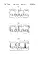
- FIG. 1illustrates a cross-section of a transistor for a memory cell located on a silicon semiconductor substrate prior to processing in accordance with the present invention.
- FIG. 2illustrates the memory cell of FIG. 1 after a layer of silicon nitride has been deposited on the cell plate.
- FIG. 3illustrates the memory cell of FIG. 1 after selective etching of the silicon nitride.
- FIG. 4illustrates the memory cell of FIG. 1 after production of an etching mask.
- FIG. 5illustrates the memory cell of FIG. 1 after anisotropic etching of a polysilicon layer with an oxide mask.
- FIG. 6illustrates the bit line via hole after processing in accordance with the present invention is complete.
- FIG. 1illustrates an insulation region and a transistor that comprises a first S/D region 3, a second S/D region 4 and a gate 5 which are produced in or, respectively, on a silicon semiconductor substrate 1.
- the gate 5is insulated from the semiconductor substrate 1 by a gate oxide (not shown) and the remaining surfaces are provided with an insulating gate encapsulation 6.
- the first S/D region 3is connected to a lower capacitor plate 7 (memory electrode) of what is referred to as a stack capacitor, this being produced from a doped polysilicon layer.
- the lower capacitor platecan also be key-shaped or crown-shaped.
- Lower capacitor plates 7 and 7' of neighboring memory cells between which a bit line contact to the second S/D region is to be producedmust be formed with sufficiently large spacing.
- a bit line contactis provided for both memory cells; the analogous case applies to memory cells having a bit line contact for each cell.
- the capacitor plates 7 and 7"are produced with a slight spacing from one another at locations where no contact to the substrate 1 is provided; the spacing is preferably so small that it is filled by the cell plate to be produced later.
- a capacitor dielectric 8is applied at least on the lower capacitor plate; what is referred to as an ONO layer is preferably produced surface-wide.
- a doped silicon layer 9 for the cell plateis then deposited, namely with such a thickness such that the small spacings are essentially filled but a depression 10 remains in the wide spacings. This depression exists only over the second S/D region.
- FIG. 2illustrates a silicon nitride layer 11 having a thickness of approximately 10-30 nm which has been deposited on the cell plate.
- a planarizing layersuch as, for example photoresist, is applied and etched back or exposed back surface-wide, so that a resist plug 16 remains only in the unfilled depression 10.
- the silicon nitride 11is etched selectively relative to the resist plug. After the removal of the resist plug 16, the underlying portion of the nitride layer 11 forms an auxiliary structure 11'. Since the nitride etching is preferably implemented anisotropically, the nitride 11'--regardless of the shape of the resist plug--extends down to the upper edge of the depression 10.
- an etching mask 14is produced, for example by an oxidation process, on the raised surface of the cell plate 9 selectively relative to the auxiliary structure 11'. The entire raised surface is then covered with silicon oxide, whereas the unoxidized, doped polysilicon remains therebelow as cell plate.
- the auxiliary structure 11'is preferably removed wet.
- the polysilicon 9is anisotropically etched with the oxide mask 14.
- the capacitor dielectric 8is selectively removed relative to the gate encapsulation 6, so that a self-aligned bit line via hole 14 is formed.
- the uncovered edge of the cell plate 9is provided with an edge insulation 13, either on the basis of a further oxidation or with a spacer.
- the capacitor dielectric 8 under the cell plateis removed either after the etching of the cell plate or during the spacer etching. In any event, the gate encapsulation 6 is not damaged during the etching of the bit line via hole 14.
- a field oxide which may be presentis likewise not attacked.
- the contactis thus self-aligned relative to the gate, relative to the field oxide, as well as relative to the upper and lower cell plate.
- the memory arrangementcan now be finished with known methods (production of a bit line 15, etc.).
- the oxidized polysilicon layer 12remains under the bit line 15 as insulation layer.
Landscapes
- Engineering & Computer Science (AREA)
- Manufacturing & Machinery (AREA)
- Semiconductor Memories (AREA)
- Electrodes Of Semiconductors (AREA)
Abstract
Description
Claims (13)
Applications Claiming Priority (2)
| Application Number | Priority Date | Filing Date | Title |
|---|---|---|---|
| DE4330471ADE4330471C1 (en) | 1993-09-08 | 1993-09-08 | Method of production for a bit-line contact hole of a memory cell |
| DE4330471.0 | 1993-09-08 |
Publications (1)
| Publication Number | Publication Date |
|---|---|
| US5500384Atrue US5500384A (en) | 1996-03-19 |
Family
ID=6497206
Family Applications (1)
| Application Number | Title | Priority Date | Filing Date |
|---|---|---|---|
| US08/294,333Expired - LifetimeUS5500384A (en) | 1993-09-08 | 1994-08-23 | Method for manufacturing a bit line via hole in a memory cell |
Country Status (6)
| Country | Link |
|---|---|
| US (1) | US5500384A (en) |
| EP (1) | EP0642159B1 (en) |
| JP (1) | JP3552758B2 (en) |
| KR (1) | KR100349986B1 (en) |
| DE (2) | DE4330471C1 (en) |
| TW (1) | TW380312B (en) |
Cited By (16)
| Publication number | Priority date | Publication date | Assignee | Title |
|---|---|---|---|---|
| US5753547A (en)* | 1997-01-28 | 1998-05-19 | Taiwan Semiconductor Manufacturing Company, Ltd. | Formation of a cylindrical polysilicon module in dram technology |
| US5776815A (en)* | 1995-09-01 | 1998-07-07 | Micron Technology, Inc. | Method for forming a contact intermediate two adjacent electrical components |
| US5780338A (en)* | 1997-04-11 | 1998-07-14 | Vanguard International Semiconductor Corporation | Method for manufacturing crown-shaped capacitors for dynamic random access memory integrated circuits |
| US6091104A (en)* | 1999-03-24 | 2000-07-18 | Chen; Chiou-Feng | Flash memory cell with self-aligned gates and fabrication process |
| US6140182A (en)* | 1999-02-23 | 2000-10-31 | Actrans System Inc. | Nonvolatile memory with self-aligned floating gate and fabrication process |
| US6165839A (en)* | 1998-06-08 | 2000-12-26 | Taiwan Semiconductor Manufacturing Company | Process to fabricate a cylindrical, capacitor structure under a bit line structure for a dynamic random access memory cell |
| US6184554B1 (en) | 1999-08-09 | 2001-02-06 | Actrans System Inc. | Memory cell with self-aligned floating gate and separate select gate, and fabrication process |
| US6222227B1 (en) | 1999-08-09 | 2001-04-24 | Actrans System Inc. | Memory cell with self-aligned floating gate and separate select gate, and fabrication process |
| US6313498B1 (en) | 1999-05-27 | 2001-11-06 | Actrans System Inc. | Flash memory cell with thin floating gate with rounded side wall, and fabrication process |
| US6344389B1 (en) | 1999-04-19 | 2002-02-05 | International Business Machines Corporation | Self-aligned damascene interconnect |
| US6344391B1 (en)* | 1997-05-29 | 2002-02-05 | Hyundai Electronics Industries Co., Ltd. | Fabrication method of semiconductor device with diagonal capacitor bit line |
| US20020081841A1 (en)* | 1998-09-03 | 2002-06-27 | Ireland Philip J. | Method of making a contact structure |
| FR2819633A1 (en)* | 2001-01-18 | 2002-07-19 | St Microelectronics Sa | Method for the integration of DRAM memory by providing a cell architecture that augments the density of integration |
| US6426896B1 (en) | 2000-05-22 | 2002-07-30 | Actrans System Inc. | Flash memory cell with contactless bit line, and process of fabrication |
| US6613684B2 (en)* | 2000-10-05 | 2003-09-02 | Oki Electric Industry Co., Ltd. | Semiconductor device and method for forming contact holes in a semiconductor device |
| US20030173565A1 (en)* | 1995-11-09 | 2003-09-18 | Micron Technology, Inc. | Method of alloying a semiconductor device |
Citations (4)
| Publication number | Priority date | Publication date | Assignee | Title |
|---|---|---|---|---|
| EP0478262A1 (en)* | 1990-09-27 | 1992-04-01 | Nec Corporation | Random access memory device and process of fabrication thereof |
| US5206183A (en)* | 1992-02-19 | 1993-04-27 | Micron Technology, Inc. | Method of forming a bit line over capacitor array of memory cells |
| US5223448A (en)* | 1991-07-18 | 1993-06-29 | Industrial Technology Research Institute | Method for producing a layered capacitor structure for a dynamic random access memory device |
| US5272103A (en)* | 1991-02-08 | 1993-12-21 | Mitsubishi Denki Kabushiki Kaisha | DRAM having a large dielectric breakdown voltage between an adjacent conductive layer and a capacitor electrode and method of manufacture thereof |
Family Cites Families (6)
| Publication number | Priority date | Publication date | Assignee | Title |
|---|---|---|---|---|
| US4855801A (en)* | 1986-08-22 | 1989-08-08 | Siemens Aktiengesellschaft | Transistor varactor for dynamics semiconductor storage means |
| JPS6384149A (en)* | 1986-09-29 | 1988-04-14 | Hitachi Ltd | Manufacture of semiconductor memory |
| JPH0279462A (en)* | 1988-09-14 | 1990-03-20 | Toshiba Corp | semiconductor storage device |
| JPH05136124A (en)* | 1991-11-08 | 1993-06-01 | Fujitsu Ltd | Semiconductor device |
| JP3149930B2 (en)* | 1992-02-07 | 2001-03-26 | 日本電気株式会社 | Semiconductor device and method of manufacturing the same |
| JPH05291531A (en)* | 1992-03-18 | 1993-11-05 | Micron Technol Inc | Method of forming a bit line over capacitor array of memory cells |
- 1993
- 1993-09-08DEDE4330471Apatent/DE4330471C1/ennot_activeExpired - Fee Related
- 1994
- 1994-08-23USUS08/294,333patent/US5500384A/ennot_activeExpired - Lifetime
- 1994-08-23TWTW083107751Apatent/TW380312B/ennot_activeIP Right Cessation
- 1994-09-05DEDE59407764Tpatent/DE59407764D1/ennot_activeExpired - Lifetime
- 1994-09-05EPEP94113868Apatent/EP0642159B1/ennot_activeExpired - Lifetime
- 1994-09-07JPJP23957494Apatent/JP3552758B2/ennot_activeExpired - Fee Related
- 1994-09-08KRKR1019940022577Apatent/KR100349986B1/ennot_activeExpired - Fee Related
Patent Citations (5)
| Publication number | Priority date | Publication date | Assignee | Title |
|---|---|---|---|---|
| EP0478262A1 (en)* | 1990-09-27 | 1992-04-01 | Nec Corporation | Random access memory device and process of fabrication thereof |
| US5135881A (en)* | 1990-09-27 | 1992-08-04 | Nec Corporation | Method of making random access memory device having memory cells each implemented by a stacked storage capacitor and a transfer transistor with lightly-doped drain structure |
| US5272103A (en)* | 1991-02-08 | 1993-12-21 | Mitsubishi Denki Kabushiki Kaisha | DRAM having a large dielectric breakdown voltage between an adjacent conductive layer and a capacitor electrode and method of manufacture thereof |
| US5223448A (en)* | 1991-07-18 | 1993-06-29 | Industrial Technology Research Institute | Method for producing a layered capacitor structure for a dynamic random access memory device |
| US5206183A (en)* | 1992-02-19 | 1993-04-27 | Micron Technology, Inc. | Method of forming a bit line over capacitor array of memory cells |
Non-Patent Citations (10)
| Title |
|---|
| "Two Step Deposited Rugged Surface (TDRS) Storagenode and Self Aligned Bitline-Contact Penetrating Cellplate (SABPEC) for 64 MbDRAM STC Cell" by Itoh, Oki Electric Industry Co., Ltd. pp. 9-10, VLSI Symposium 1991. |
| Article "A Self-Aligned Contact Process With Improved Surface Planarization" by Kusters et al, Journal De Physique, Cr, Tome 49, Sep. 1988 at C4-503. |
| Article A Self Aligned Contact Process With Improved Surface Planarization by Kusters et al, Journal De Physique, Cr, Tome 49, Sep. 1988 at C4 503.* |
| Patent Abstracts of Japan, vol. 12, No. 320 ( 651)(3167), JP 63 84149 (Hitachi Ltd.) Apr. 14, 1988.* |
| Patent Abstracts of Japan, vol. 12, No. 320 (-651)(3167), JP 63-84149 (Hitachi Ltd.) Apr. 14, 1988. |
| Patent Abstracts of Japan, vol. 17, No. 514 (E 1433), 1 Jun. 1993 JP A 05 136 124 (Fujitsu Ltd).* |
| Patent Abstracts of Japan, vol. 17, No. 514 (E-1433), 1 Jun. 1993 JP A-05 136 124 (Fujitsu Ltd). |
| Patent Abstracts of Japan, vol. 17, No. 672 (E 1474), JP A 05 226 583 (NEC Corp) 3, Sep. 1993.* |
| Patent Abstracts of Japan, vol. 17, No. 672 (E-1474), JP-A-05 226 583 (NEC Corp) 3, Sep. 1993. |
| Two Step Deposited Rugged Surface (TDRS) Storagenode and Self Aligned Bitline Contact Penetrating Cellplate (SABPEC) for 64 MbDRAM STC Cell by Itoh, Oki Electric Industry Co., Ltd. pp. 9 10, VLSI Symposium 1991.* |
Cited By (24)
| Publication number | Priority date | Publication date | Assignee | Title |
|---|---|---|---|---|
| US5776815A (en)* | 1995-09-01 | 1998-07-07 | Micron Technology, Inc. | Method for forming a contact intermediate two adjacent electrical components |
| US6100156A (en)* | 1995-09-01 | 2000-08-08 | Micron Technology, Inc. | Method for forming a contact intermediate two adjacent electrical components |
| US20030173565A1 (en)* | 1995-11-09 | 2003-09-18 | Micron Technology, Inc. | Method of alloying a semiconductor device |
| US5753547A (en)* | 1997-01-28 | 1998-05-19 | Taiwan Semiconductor Manufacturing Company, Ltd. | Formation of a cylindrical polysilicon module in dram technology |
| US5780338A (en)* | 1997-04-11 | 1998-07-14 | Vanguard International Semiconductor Corporation | Method for manufacturing crown-shaped capacitors for dynamic random access memory integrated circuits |
| US6344391B1 (en)* | 1997-05-29 | 2002-02-05 | Hyundai Electronics Industries Co., Ltd. | Fabrication method of semiconductor device with diagonal capacitor bit line |
| US6165839A (en)* | 1998-06-08 | 2000-12-26 | Taiwan Semiconductor Manufacturing Company | Process to fabricate a cylindrical, capacitor structure under a bit line structure for a dynamic random access memory cell |
| US8680595B2 (en) | 1998-09-03 | 2014-03-25 | Micron Technology, Inc. | Sleeve insulators and semiconductor device including the same |
| US7968403B2 (en)* | 1998-09-03 | 2011-06-28 | Micron Technology, Inc. | Method of fabricating a sleeve insulator for a contact structure |
| US20070004199A1 (en)* | 1998-09-03 | 2007-01-04 | Ireland Philip J | Method of making a contact structure |
| US20020081841A1 (en)* | 1998-09-03 | 2002-06-27 | Ireland Philip J. | Method of making a contact structure |
| US6140182A (en)* | 1999-02-23 | 2000-10-31 | Actrans System Inc. | Nonvolatile memory with self-aligned floating gate and fabrication process |
| US6091104A (en)* | 1999-03-24 | 2000-07-18 | Chen; Chiou-Feng | Flash memory cell with self-aligned gates and fabrication process |
| US6291297B1 (en) | 1999-03-24 | 2001-09-18 | Actrans System Inc. | Flash memory cell with self-aligned gates and fabrication process |
| US6344389B1 (en) | 1999-04-19 | 2002-02-05 | International Business Machines Corporation | Self-aligned damascene interconnect |
| US6313498B1 (en) | 1999-05-27 | 2001-11-06 | Actrans System Inc. | Flash memory cell with thin floating gate with rounded side wall, and fabrication process |
| US6590253B2 (en) | 1999-08-09 | 2003-07-08 | Actrans System Inc. | Memory cell with self-aligned floating gate and separate select gate, and fabrication process |
| US6184554B1 (en) | 1999-08-09 | 2001-02-06 | Actrans System Inc. | Memory cell with self-aligned floating gate and separate select gate, and fabrication process |
| US6222227B1 (en) | 1999-08-09 | 2001-04-24 | Actrans System Inc. | Memory cell with self-aligned floating gate and separate select gate, and fabrication process |
| US6426896B1 (en) | 2000-05-22 | 2002-07-30 | Actrans System Inc. | Flash memory cell with contactless bit line, and process of fabrication |
| US6503785B2 (en) | 2000-05-22 | 2003-01-07 | Actrans System Inc. | Flash memory cell with contactless bit line, and process of fabrication |
| US6613684B2 (en)* | 2000-10-05 | 2003-09-02 | Oki Electric Industry Co., Ltd. | Semiconductor device and method for forming contact holes in a semiconductor device |
| FR2819633A1 (en)* | 2001-01-18 | 2002-07-19 | St Microelectronics Sa | Method for the integration of DRAM memory by providing a cell architecture that augments the density of integration |
| US6759304B2 (en) | 2001-01-18 | 2004-07-06 | Stmicroelectronics Sa | DRAM memory integration method |
Also Published As
| Publication number | Publication date |
|---|---|
| JP3552758B2 (en) | 2004-08-11 |
| KR100349986B1 (en) | 2002-12-11 |
| EP0642159A1 (en) | 1995-03-08 |
| KR950010053A (en) | 1995-04-26 |
| DE4330471C1 (en) | 1994-10-20 |
| TW380312B (en) | 2000-01-21 |
| JPH07153853A (en) | 1995-06-16 |
| DE59407764D1 (en) | 1999-03-18 |
| EP0642159B1 (en) | 1999-02-03 |
Similar Documents
| Publication | Publication Date | Title |
|---|---|---|
| US6566241B2 (en) | Method of forming metal contact in semiconductor device | |
| KR0170312B1 (en) | Highly Integrated DRAM Cells and Manufacturing Method Thereof | |
| US7807569B2 (en) | Method of manufacturing a contact structure for a semiconductor device | |
| KR100726145B1 (en) | Semiconductor device manufacturing method | |
| US5500384A (en) | Method for manufacturing a bit line via hole in a memory cell | |
| JPH0982920A (en) | Highly integrated DRAM cell manufacturing method | |
| KR100273987B1 (en) | DRAM device and manufacturing method | |
| JP2557592B2 (en) | Method of manufacturing semiconductor memory cell | |
| KR100466750B1 (en) | Semiconductor device and its manufacturing method | |
| US5723374A (en) | Method for forming dielectric spacer to prevent poly stringer in stacked capacitor DRAM technology | |
| KR0141950B1 (en) | Manufacturing method of semiconductor device | |
| US6228762B1 (en) | Methods for forming contact holes having sidewalls with smooth profiles | |
| US20070020844A1 (en) | Method for fabricating bit line of memory device | |
| US5536671A (en) | Method for fabricating capacitor of a semiconductor device | |
| KR100563789B1 (en) | Integrated circuit manufacturing method | |
| US6136642A (en) | Method of making a dynamic random access memory | |
| JPH0834303B2 (en) | Method for manufacturing semiconductor memory device | |
| US6175132B1 (en) | Semiconductor memory device and method of fabricating the same | |
| JP3039438B2 (en) | Semiconductor memory device and method of manufacturing the same | |
| KR0141949B1 (en) | Manufacturing method of semiconductor device | |
| JP2753092B2 (en) | Method for manufacturing semiconductor memory device | |
| KR0158906B1 (en) | Manufacture of semiconductor memory device | |
| JP3398056B2 (en) | Semiconductor device and manufacturing method thereof | |
| JP2509912B2 (en) | Method for manufacturing semiconductor memory device | |
| JP3199044B2 (en) | Semiconductor device and manufacturing method thereof |
Legal Events
| Date | Code | Title | Description |
|---|---|---|---|
| AS | Assignment | Owner name:SIEMENS AKTIENGESELLSCHAFT, GERMANY Free format text:ASSIGNMENT OF ASSIGNORS INTEREST;ASSIGNOR:MELZNER, HANNO;REEL/FRAME:007104/0390 Effective date:19940810 | |
| STCF | Information on status: patent grant | Free format text:PATENTED CASE | |
| FEPP | Fee payment procedure | Free format text:PAYOR NUMBER ASSIGNED (ORIGINAL EVENT CODE: ASPN); ENTITY STATUS OF PATENT OWNER: LARGE ENTITY | |
| FPAY | Fee payment | Year of fee payment:4 | |
| FEPP | Fee payment procedure | Free format text:PAYOR NUMBER ASSIGNED (ORIGINAL EVENT CODE: ASPN); ENTITY STATUS OF PATENT OWNER: LARGE ENTITY Free format text:PAYER NUMBER DE-ASSIGNED (ORIGINAL EVENT CODE: RMPN); ENTITY STATUS OF PATENT OWNER: LARGE ENTITY | |
| FPAY | Fee payment | Year of fee payment:8 | |
| FPAY | Fee payment | Year of fee payment:12 | |
| AS | Assignment | Owner name:INFINEON TECHNOLOGIES AG,GERMANY Free format text:ASSIGNMENT OF ASSIGNORS INTEREST;ASSIGNOR:SIEMENS AKTIENGESELLSCHAFT;REEL/FRAME:024120/0587 Effective date:19990331 | |
| XAS | Not any more in us assignment database | Free format text:ASSIGNMENT OF ASSIGNORS INTEREST;ASSIGNOR:SIEMENS AKTIENGESELLSCHAFT;REEL/FRAME:023957/0001 | |
| AS | Assignment | Owner name:QIMONDA AG,GERMANY Free format text:ASSIGNMENT OF ASSIGNORS INTEREST;ASSIGNOR:INFINEON TECHNOLOGIES AG;REEL/FRAME:024016/0001 Effective date:20060425 |