US5498883A - Superluminescent edge emitting device with apparent vertical light emission and method of making - Google Patents
Superluminescent edge emitting device with apparent vertical light emission and method of makingDownload PDFInfo
- Publication number
- US5498883A US5498883AUS08/317,110US31711094AUS5498883AUS 5498883 AUS5498883 AUS 5498883AUS 31711094 AUS31711094 AUS 31711094AUS 5498883 AUS5498883 AUS 5498883A
- Authority
- US
- United States
- Prior art keywords
- light emitting
- sidewalls
- emitting portion
- superluminescent
- major surface
- Prior art date
- Legal status (The legal status is an assumption and is not a legal conclusion. Google has not performed a legal analysis and makes no representation as to the accuracy of the status listed.)
- Expired - Fee Related
Links
Images
Classifications
- H—ELECTRICITY
- H10—SEMICONDUCTOR DEVICES; ELECTRIC SOLID-STATE DEVICES NOT OTHERWISE PROVIDED FOR
- H10H—INORGANIC LIGHT-EMITTING SEMICONDUCTOR DEVICES HAVING POTENTIAL BARRIERS
- H10H20/00—Individual inorganic light-emitting semiconductor devices having potential barriers, e.g. light-emitting diodes [LED]
- H10H20/80—Constructional details
- H10H20/81—Bodies
- H10H20/814—Bodies having reflecting means, e.g. semiconductor Bragg reflectors
- H10H20/8142—Bodies having reflecting means, e.g. semiconductor Bragg reflectors forming resonant cavity structures
- H—ELECTRICITY
- H10—SEMICONDUCTOR DEVICES; ELECTRIC SOLID-STATE DEVICES NOT OTHERWISE PROVIDED FOR
- H10H—INORGANIC LIGHT-EMITTING SEMICONDUCTOR DEVICES HAVING POTENTIAL BARRIERS
- H10H20/00—Individual inorganic light-emitting semiconductor devices having potential barriers, e.g. light-emitting diodes [LED]
- H10H20/042—Superluminescent diodes
- H—ELECTRICITY
- H10—SEMICONDUCTOR DEVICES; ELECTRIC SOLID-STATE DEVICES NOT OTHERWISE PROVIDED FOR
- H10H—INORGANIC LIGHT-EMITTING SEMICONDUCTOR DEVICES HAVING POTENTIAL BARRIERS
- H10H20/00—Individual inorganic light-emitting semiconductor devices having potential barriers, e.g. light-emitting diodes [LED]
- H10H20/80—Constructional details
- H10H20/862—Resonant cavity structures
Definitions
- the present inventionrelates, in general, to semiconductor devices, and more particularly to superluminescent light emitting devices (LEDs).
- LEDssuperluminescent light emitting devices
- Superluminescent LEDscombine high efficiency with a broad spectral bandwidth. These characteristics are important for achieving high performance in applications such as a light source for fiber-optic gyroscopes. Another application for such devices is in a display matrix in which light from several hundred devices is combined to form an image. LEDs which operate in the lasing mode produce an undesirable "speckle" effect in an image due to coherent wave interference. The broad spectral bandwidth of a superluminescent LEDs precludes coherent wave interference effects.
- superluminescent LEDshave been edge emitting devices where the light is emitted parallel to the surface of the semiconductor substrate in which the superluminescent LEDs are fabricated.
- production of light through the top surface of a light emitting device or perpendicular to the semiconductor substrate surfaceis highly desirable.
- Superluminescent LEDs which emit light perpendicular to the substrate surfacemay be integrated with devices having other functions on a single integrated circuit chip. Also, large arrays of similar such devices may be fabricated on a single substrate to provide an economical, high efficiency, planar display.
- edge-emitting superluminescent LEDs used in the pastcannot be integrated with other semiconductor devices on the same chip.
- Superluminescent LEDsoperate in a regime between lasing and spontaneous emission. Lasing is undesirable in a superluminescent LED. In the past, there have been difficulties in preventing superluminescent LEDs from lasing within a certain temperature range. In the past, lasing has been prevented by the use of anti-reflective coatings formed on at least one of the facets of an edge-emitting device through which light is emitted. However, driving the superluminescent LEDs to high powers may eventually cause lasing, in spite of the presence of the anti-reflective coating. Because even the best anti-reflective coating will reflect some proportion of the light impinging on it, lasing will eventually occur in the prior art superluminescent LEDs if the power is increased to a high enough level.
- Superluminescent LEDsprovide high efficiency and freedom from wave interference effects, and superluminescent LEDs which emit light perpendicular to the substrate surface facilitate economical manufacturing, testing, and packaging. There is still a need to fabricate more efficient superluminescent LEDs that do not lase at high power levels and that can be integrated with other devices on the same chip.
- a superluminescent edge emitting deviceis fabricated to have apparent vertical light emission.
- the superluminescent deviceis fabricated to be comprised of a semiconductor supporting structure having a major surface.
- a light emitting portionis formed above a first portion of the major surface, wherein the light emitting portion is configured in a substantially circular shape to suppress lasing and has sidewalls, and wherein a light is emitted from the sidewalls of the light emitting portion.
- An non-emitting portionis formed above a second portion of the major surface and adjacent to the light emitting portion, wherein the non-emitting portion has sidewalls, and wherein the sidewalls of the light emitting portion and the sidewalls of the non-emitting portion are configured to direct the light emitted from the light emitting portion substantially perpendicular to the major surface.
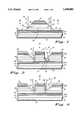
- FIG. 1illustrates an enlarged, cross-sectional view of a superluminescent LED according to a first embodiment of the present invention
- FIG. 2illustrates an enlarged, cross-sectional view of a superluminescent LED according to a second embodiment of the present invention
- FIG. 3illustrates an enlarged, cross-sectional view of a superluminescent LED according to a third embodiment of the present invention.
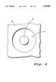
- FIG. 4illustrates an enlarged, top view of the second embodiment of the present invention.
- FIG. 1illustrates a simplified, enlarged cross-section view of a first embodiment of the present invention.
- a superluminescent LEDcomprised of a supporting structure 10 of a first conductivity type having a first major surface 11 and a second major surface 9.
- First major surface 11defines a horizontal plane of the superluminescent LED.
- supporting structure 10is comprised of a semiconductor substrate. More preferably, the semiconductor substrate is comprised of gallium arsenide (GaAs) and is doped n-type with an n-type dopant such as Selenium (Se). Other suitable dopants may be used.
- GaAsgallium arsenide
- SeSelenium
- Other suitable dopantsmay be used.
- An alternative embodimentutilizes a p-type substrate so that first mirror stack 14 may be heavily doped p-type to improve the flow of bias current through the superluminescent LED.
- Supporting structure 10 and subsequent epitaxial layers formed on supporting structure 10may be comprised of other III-V semiconductor materials systems such as indium phosphide.
- buffer layer 12 of the first conductivity typeserves to smooth the top surface of semiconductor substrate 22.
- buffer layer 12is comprised of a n-type GaAs layer or an aluminum gallium arsenide layer (AlGaAs). Buffer layer 12 is not absolutely necessary to obtain a working device, however, buffer layer 12 may be used to obtain better epitaxial growth of subsequent layers.
- First mirror stack 14is also referred to as a 1/4 wave stack or distributed Bragg reflector in the art.
- First mirror stack 14is comprised a superlattice structure in which a plurality of alternating layers of semiconductor materials are formed with matching crystal structures. The materials used in first mirror stack 14 must be transparent at the lasing wavelength.
- first mirror stack 14is comprised of alternating layers of n-type aluminum arsenide (AlAs) and n-type GaAs.
- AlAsaluminum arsenide
- the thickness of each layeris preferably equal to 1/4 of the wavelength of operation divided by the refractive index. The number of periods or pairs of alternating layers determines the reflectivity of the device.
- a bottom cladding layer 16 of the first conductivity typeis formed on first mirror stack 14.
- Bottom cladding layer 16provides a region having a wide bandgap which serves to confine holes and electrons within an active layer 18 which is formed on bottom cladding layer 16.
- bottom cladding layer 16is comprised of AlGaAs.
- Active layer 18is preferably comprised of barrier layers and at least one light emitting region (quantum well).
- the light emitting regionis preferably comprised of nominally undoped indium gallium arsenide (InGaAs). Multiple light emitting regions may be used. In addition, other materials, such as GaAs, may be used for different operating wavelengths, with appropriate changes to the composition of first mirror stack 14 so that the layers are transparent at the operating wavelength.
- the formation of light emitting regions and barrier layersis well known in the art.
- the total thickness of active layer 18must be a multiple of 1/2 of the wavelength of operation in order for active layer 18 to fulfill phase matching requirements in the optical cavity, which is comprised of all the layers between first mirror stack 14 and second mirror stack 24 (described below).
- the light emitting regions which comprise active layer 18serve to emit light when a bias current is applied to them.
- top cladding layer 20 of a second conductivity typeis formed on active layer 18.
- Top cladding layer 20is similar in structure and function to bottom cladding layer 16.
- Second mirror stack 24is typically similar in structure to first mirror stack 14, except that it is of the opposite conductivity type.
- An alternative embodimentutilizes a dielectric mirror for second mirror stack 24.
- the dielectric mirrormay be comprised of alternating layers of silicon/silicon dioxide (Si/SiO 2 ) or silicon/silicon nitride (Si/SiN x ).
- a second conductivity type ohmic contact 30is formed and patterned on second mirror stack 24.
- the fabrication and use of ohmic contacts, in general,is well known in the art.
- Ohmic contact 30is typically comprised of a gold alloy.
- Ohmic contact 30serves as a contact means whereby a bias current may be applied to the superluminescent LED and thus applied to active layer 18.
- Portions of second mirror stack 24, top cladding layer 20, active layer 18 and bottom cladding layer 16are etched to form an emitting portion 60 and a non-emitting portion 62.
- the etchmust be performed at least down to first mirror stack 14. Note that non-emitting portion 62 is adjacent to light emitting portion 60.
- Sidewalls 61 and 63are configured to direct the in-plane luminescence substantially perpendicular to major surface 11.
- sidewalls 61 and 63form an oblique or acute angle.
- FIG. 1illustrates the first embodiment where emitting portion 60 has sidewalls 61 which are at an angle of approximately 135° from major surface 11 and sidewalls 63 are parallel (or at an angle of 0°) to major surface 11. The angle of 135° is shown by line 25.
- Isotropic etching to obtain the aforementioned slope of sidewalls 61can be achieved by a wet etch, dry etch, or by ion milling.
- Ohmic contact 30may be used as a mask during this etch if desired.
- Dry etchingcan be done by using reactive ion etching (RIE) or reactive ion beam etching (RIBE).
- RIEreactive ion etching
- RIBEreactive ion beam etching
- FIG. 2illustrates a second embodiment where sidewalls 61 are substantially perpendicular (or at an angle of 90°) to major surface 11 and sidewalls 63 at an angle of approximately 45° from major surface 11.
- the angle of 90°is shown by line 33 and the angle of 45° is shown by line 35.
- Sidewalls 63 at an angle greater than 0° from major surface 11 and sidewalls 61 at an angle of 90° from major surface 11can be achieved by RIBE.
- a combination of the embodiments of FIGS. 1 and 2would provide a superluminescent LED with sidewalls 61 at an angle of 135° from major surface 11 and sidewalls 63 at an angle of 45° from major surface 11.
- FIG. 1Emission of light takes place in the horizontal direction as shown by emitting light 75 shown in FIGS. 1, 2, and 3.
- light 75is emitted from emitting portion 60 in a downward direction and reflected off of first mirror stack 14 to be directed substantially perpendicular to major surface 11.
- the embodiment of FIG. 1is desirable from the standpoint that it is easily manufactured.
- FIG. 2illustrates a preferred embodiment of the present invention. The structure of FIG. 2 is preferred because the apparent emission of light 75 substantially perpendicular to major surface 11 is enhanced.
- light 75is reflected off of sidewalls 63 of non-emitting portion 62 and reflected substantially perpendicular to first major surface 11.
- FIG. 2illustrates an embodiment having a reflective layer 70 formed on sidewalls 63.
- Reflective layer 70acts to reflect more emitting light 75 substantially perpendicular to major surface 11.
- Reflective layer 70is preferably formed at the same time ohmic contact 30 is formed and of the same material as ohmic contact 30. However, other materials may be used.
- reflective layer 70may be comprised of a dielectric stack. Reflective layer 70 is not be absolutely necessary to form a working device.
- FIG. 3illustrates an alternate embodiment of the embodiment shown in FIG. 2. This structure is similar to that shown in FIG. 2 except that, in this embodiment, sidewalls 63 are curved to better focus light 75 substantially perpendicular to major surface 11. Curved sidewalls 63 can be formed by RIBE.
- the reflectivities of the first and the second mirror stacksare chosen to be nearly 100% so as to achieve lasing in the vertical direction.
- the reflectivitiesare chosen to be less than 100% because lasing is undesirable.
- the first and second mirror stacks 16 and 20 of the present inventionare fabricated to enhance superluminescent behavior by confining emitted photons to the plane of active layer 18 (also referred to as the gain region).
- Superluminescent operation horizontal to the plane of major surface 11is favored because of the longer optical path length for photons propagating in the horizontal plane.
- the reduced mirror stack reflectivitiessuppress lasing or strongly superluminescent operation vertical to the plane of major surface 11.
- FIG. 4illustrates an enlarged, highly simplified top view of the embodiment shown in FIG. 2.
- the superluminescent LED of the present inventionis preferably configured so that lasing is suppressed.
- the configuration of emitting portion 60 of the superluminescent LEDis substantially circular. Lasing in the plane horizontal to major surface 11 is suppressed because of the circular shape of light emitting portion 60, which corresponds to a resonator configuration that is not stable.
- the circleis preferably 2-20 micrometers in diameter measured in active layer 18. If the circle is too large, lasing may take place. If the circle is too small, superluminescent emission may be reduced.
- Substantially circularmeans that the configuration of active portion 60 can be a polygon which is substantially circular.
- an anti-reflective coating 80(shown in FIG. 3) may be formed on sidewalls 61 to further suppress lasing.
- This anti-reflective coating 80may be comprised of silicon nitride or other suitable materials. The formation of anti-reflective coatings, in general, is well known in the art.
- a first conductivity type ohmic contact 31is formed on second major surface 9 of supporting structure 10, as is shown in FIGS. 1, 2, and 3.
- the superluminescent LEDprovided by this invention combines the advantages of superluminescence with the advantages of surface emitting devices. Although a true surface emitting device is not fabricated, the superluminescent LED of the present invention emits light substantially perpendicular to major surface 11. Like a surface emitting device, the superluminescent LED of the present invention is easy to build, package and test. The superluminescent LED of the present invention may be easily fabricated as part of a large array of such superluminescent LEDs or as part of a larger integrated circuit.
Landscapes
- Led Devices (AREA)
Abstract
Description
Claims (25)
Priority Applications (1)
| Application Number | Priority Date | Filing Date | Title |
|---|---|---|---|
| US08/317,110US5498883A (en) | 1992-08-05 | 1994-10-03 | Superluminescent edge emitting device with apparent vertical light emission and method of making |
Applications Claiming Priority (2)
| Application Number | Priority Date | Filing Date | Title |
|---|---|---|---|
| US92505392A | 1992-08-05 | 1992-08-05 | |
| US08/317,110US5498883A (en) | 1992-08-05 | 1994-10-03 | Superluminescent edge emitting device with apparent vertical light emission and method of making |
Related Parent Applications (1)
| Application Number | Title | Priority Date | Filing Date |
|---|---|---|---|
| US92505392AContinuation | 1992-08-05 | 1992-08-05 |
Publications (1)
| Publication Number | Publication Date |
|---|---|
| US5498883Atrue US5498883A (en) | 1996-03-12 |
Family
ID=25451137
Family Applications (1)
| Application Number | Title | Priority Date | Filing Date |
|---|---|---|---|
| US08/317,110Expired - Fee RelatedUS5498883A (en) | 1992-08-05 | 1994-10-03 | Superluminescent edge emitting device with apparent vertical light emission and method of making |
Country Status (4)
| Country | Link |
|---|---|
| US (1) | US5498883A (en) |
| EP (1) | EP0582078B1 (en) |
| JP (1) | JPH06104483A (en) |
| DE (1) | DE69329223T2 (en) |
Cited By (62)
| Publication number | Priority date | Publication date | Assignee | Title |
|---|---|---|---|---|
| US5606181A (en)* | 1994-03-29 | 1997-02-25 | Ricoh Company, Ltd. | Edge emitting type light emitting diode array heads |
| US5631474A (en)* | 1994-11-11 | 1997-05-20 | Ricoh Company, Ltd. | Light emitting element and array of light emitting elements for light source |
| US5811319A (en)* | 1995-03-27 | 1998-09-22 | Toyoda Gosei Co., Ltd. | Methods of forming electrodes on gallium nitride group compound semiconductors |
| US5955748A (en)* | 1994-07-19 | 1999-09-21 | Oki Electric Industry Co., Ltd. | End face light emitting type light emitting diode |
| US6025213A (en)* | 1994-12-29 | 2000-02-15 | Sony Corporation | Semiconductor light-emitting device package and method of manufacturing the same |
| US6150667A (en)* | 1996-05-22 | 2000-11-21 | Nec Corporation | Semiconductor optical modulator |
| US6222871B1 (en) | 1998-03-30 | 2001-04-24 | Bandwidth9 | Vertical optical cavities produced with selective area epitaxy |
| US6226425B1 (en) | 1999-02-24 | 2001-05-01 | Bandwidth9 | Flexible optical multiplexer |
| US6233263B1 (en) | 1999-06-04 | 2001-05-15 | Bandwidth9 | Monitoring and control assembly for wavelength stabilized optical system |
| US6275513B1 (en) | 1999-06-04 | 2001-08-14 | Bandwidth 9 | Hermetically sealed semiconductor laser device |
| US6366597B1 (en) | 1998-04-14 | 2002-04-02 | Bandwidth9 Inc. | Lattice-relaxed vertical optical cavities |
| US6367949B1 (en) | 1999-08-04 | 2002-04-09 | 911 Emergency Products, Inc. | Par 36 LED utility lamp |
| US20020041499A1 (en)* | 1999-06-08 | 2002-04-11 | Pederson John C. | LED warning signal light and row of led's |
| US6380865B1 (en) | 1999-04-06 | 2002-04-30 | 911 Emergency Products, Inc. | Replacement led lamp assembly and modulated power intensity for light source |
| US6424269B1 (en) | 1997-10-21 | 2002-07-23 | 911 Emergency Products, Inc. | LED warning signal light and light bar |
| US20020142506A1 (en)* | 2001-03-30 | 2002-10-03 | Seiko Epson Corporation | Surface emission type semiconductor light-emitting device and method of manufacturing the same |
| US6462669B1 (en) | 1999-04-06 | 2002-10-08 | E. P . Survivors Llc | Replaceable LED modules |
| US6487231B1 (en) | 1998-04-14 | 2002-11-26 | Bandwidth 9, Inc. | Vertical cavity apparatus with tunnel junction |
| US6487230B1 (en) | 1998-04-14 | 2002-11-26 | Bandwidth 9, Inc | Vertical cavity apparatus with tunnel junction |
| US20020176251A1 (en)* | 2001-05-23 | 2002-11-28 | Ivoclar Vivadent Ag | Lighting apparatus for guiding light onto a light polymerizable piece to effect hardening thereof |
| US6493373B1 (en) | 1998-04-14 | 2002-12-10 | Bandwidth 9, Inc. | Vertical cavity apparatus with tunnel junction |
| US6493372B1 (en) | 1998-04-14 | 2002-12-10 | Bandwidth 9, Inc. | Vertical cavity apparatus with tunnel junction |
| US6493371B1 (en) | 1998-04-14 | 2002-12-10 | Bandwidth9, Inc. | Vertical cavity apparatus with tunnel junction |
| US6535541B1 (en) | 1998-04-14 | 2003-03-18 | Bandwidth 9, Inc | Vertical cavity apparatus with tunnel junction |
| US6547410B1 (en) | 2000-07-28 | 2003-04-15 | 911 Emergency Products, Inc. | LED alley/take-down light |
| US6590343B2 (en) | 2000-06-06 | 2003-07-08 | 911Ep, Inc. | LED compensation circuit |
| US6590502B1 (en) | 1992-10-12 | 2003-07-08 | 911Ep, Inc. | Led warning signal light and movable support |
| US20030152125A1 (en)* | 2002-02-13 | 2003-08-14 | Junichi Kinoshita | Surface emitting laser and semiconductor light emitting device |
| US6614359B2 (en) | 1999-04-06 | 2003-09-02 | 911 Emergency Products, Inc. | Replacement led lamp assembly and modulated power intensity for light source |
| US6700502B1 (en) | 1999-06-08 | 2004-03-02 | 911Ep, Inc. | Strip LED light assembly for motor vehicle |
| US6760357B1 (en) | 1998-04-14 | 2004-07-06 | Bandwidth9 | Vertical cavity apparatus with tunnel junction |
| US20040199785A1 (en)* | 2002-08-23 | 2004-10-07 | Pederson John C. | Intelligent observation and identification database system |
| US6835992B1 (en)* | 1996-02-01 | 2004-12-28 | Optical Communication Products, Inc. | Closely-spaced VCSEL and photodetector for applications requiring their independent operation |
| US20050047167A1 (en)* | 1999-08-04 | 2005-03-03 | Pederson John C. | Warning signal light bar |
| US20050057941A1 (en)* | 1999-08-04 | 2005-03-17 | 911Ep, Inc. | 360 Degree pod warning light signal |
| US20050161679A1 (en)* | 2004-01-27 | 2005-07-28 | Decai Sun | Semiconductor light emitting devices including current spreading layers |
| US7046160B2 (en) | 2000-11-15 | 2006-05-16 | Pederson John C | LED warning light and communication system |
| US20060139985A1 (en)* | 2002-10-30 | 2006-06-29 | Kabushiki Kaisha Toshiba | Non-volatile semiconductor storage device performing ROM read operation upon power-on |
| US20070000536A1 (en)* | 2005-01-19 | 2007-01-04 | Yasha Yi | Light trapping in thin film solar cells using textured photonic crystal |
| US20070001183A1 (en)* | 2005-07-01 | 2007-01-04 | Shi-Ming Chen | Light-emitting diode |
| US7163324B2 (en) | 1999-06-08 | 2007-01-16 | 911Ep, Inc. | Led light stick assembly |
| US20070096133A1 (en)* | 2005-11-02 | 2007-05-03 | Lee Kian S | System and method for LED manufacturing |
| US20090078948A1 (en)* | 2004-11-18 | 2009-03-26 | Koninklijke Philips Electronics, N.V. | Illuminator and method for producing such illuminator |
| US20100085772A1 (en)* | 2008-10-08 | 2010-04-08 | Samsung Electro-Mechanics Co., Ltd. | Side-view type light emitting device and optical device including the same |
| US20110063585A1 (en)* | 2009-09-11 | 2011-03-17 | Seiko Epson Corporation | Projector |
| US20120091491A1 (en)* | 2001-03-15 | 2012-04-19 | Osram Opto Semiconductors Gmbh | Radiation-Emitting Optical Component |
| US8188879B2 (en) | 2007-05-24 | 2012-05-29 | Federal Law Enforcement Development Services, Inc. | LED light global positioning and routing communication system |
| US8188878B2 (en) | 2000-11-15 | 2012-05-29 | Federal Law Enforcement Development Services, Inc. | LED light communication system |
| US8543505B2 (en) | 2011-01-14 | 2013-09-24 | Federal Law Enforcement Development Services, Inc. | Method of providing lumens and tracking of lumen consumption |
| US8840287B2 (en) | 2012-02-16 | 2014-09-23 | Toyota Motor Engineering & Manufacturing North America, Inc. | Interior automotive components with illuminated reflective surface |
| US8890773B1 (en) | 2009-04-01 | 2014-11-18 | Federal Law Enforcement Development Services, Inc. | Visible light transceiver glasses |
| US9100124B2 (en) | 2007-05-24 | 2015-08-04 | Federal Law Enforcement Development Services, Inc. | LED Light Fixture |
| US9258864B2 (en) | 2007-05-24 | 2016-02-09 | Federal Law Enforcement Development Services, Inc. | LED light control and management system |
| US9265112B2 (en) | 2013-03-13 | 2016-02-16 | Federal Law Enforcement Development Services, Inc. | LED light control and management system |
| US9294198B2 (en) | 2007-05-24 | 2016-03-22 | Federal Law Enforcement Development Services, Inc. | Pulsed light communication key |
| US9414458B2 (en) | 2007-05-24 | 2016-08-09 | Federal Law Enforcement Development Services, Inc. | LED light control assembly and system |
| US9455783B2 (en) | 2013-05-06 | 2016-09-27 | Federal Law Enforcement Development Services, Inc. | Network security and variable pulse wave form with continuous communication |
| US10448472B2 (en) | 2015-08-11 | 2019-10-15 | Federal Law Enforcement Development Services, Inc. | Function disabler device and system |
| DE102019100532A1 (en)* | 2019-01-10 | 2020-07-16 | Osram Opto Semiconductors Gmbh | RADIATION-EMITTING SEMICONDUCTOR CHIP AND METHOD FOR PRODUCING A RADIATION-EMITTING SEMICONDUCTOR CHIP |
| US11265082B2 (en) | 2007-05-24 | 2022-03-01 | Federal Law Enforcement Development Services, Inc. | LED light control assembly and system |
| DE102020122210A1 (en) | 2020-08-25 | 2022-03-03 | OSRAM Opto Semiconductors Gesellschaft mit beschränkter Haftung | Method for producing a radiation-emitting semiconductor chip and radiation-emitting semiconductor chip |
| US11783345B2 (en) | 2014-01-15 | 2023-10-10 | Federal Law Enforcement Development Services, Inc. | Cyber life electronic networking and commerce operating exchange |
Families Citing this family (6)
| Publication number | Priority date | Publication date | Assignee | Title |
|---|---|---|---|---|
| DE19727233A1 (en)* | 1997-06-26 | 1999-01-07 | Siemens Ag | Radiation-emitting optoelectronic component |
| EP0905797B1 (en)* | 1997-09-29 | 2010-02-10 | OSRAM Opto Semiconductors GmbH | Semiconductor light source and method of fabrication |
| WO2000045443A1 (en)* | 1999-01-28 | 2000-08-03 | Nova Crystals, Inc. | High performance light emitting diodes |
| JP4868709B2 (en)* | 2004-03-09 | 2012-02-01 | 三洋電機株式会社 | Light emitting element |
| JP2011204888A (en)* | 2010-03-25 | 2011-10-13 | Panasonic Corp | Light-emitting device and backlight module using the same |
| DE102016116468A1 (en)* | 2016-09-02 | 2018-03-08 | Osram Opto Semiconductors Gmbh | OPTOELECTRONIC ARRANGEMENT |
Citations (15)
| Publication number | Priority date | Publication date | Assignee | Title |
|---|---|---|---|---|
| US3443140A (en)* | 1965-04-06 | 1969-05-06 | Gen Electric | Light emitting semiconductor devices of improved transmission characteristics |
| US3821775A (en)* | 1971-09-23 | 1974-06-28 | Spectronics Inc | Edge emission gaas light emitter structure |
| US3883772A (en)* | 1972-05-02 | 1975-05-13 | Matsushita Electronics Corp | Electric light-emitting apparatus |
| WO1985003809A1 (en)* | 1984-02-23 | 1985-08-29 | Codenoll Technology Corporation | Edge-emitting light emitting diode |
| US4634928A (en)* | 1985-04-19 | 1987-01-06 | Trw Inc. | Superluminescent light-emitting diode and related method |
| US4636821A (en)* | 1983-02-21 | 1987-01-13 | Nec Corporation | Surface-emitting semiconductor elements |
| JPS6373572A (en)* | 1986-09-16 | 1988-04-04 | Nec Corp | Edge-emitting light-emitting diode |
| US4821276A (en)* | 1987-04-20 | 1989-04-11 | General Electric Company | Super-luminescent diode |
| US4872180A (en)* | 1989-06-16 | 1989-10-03 | Gte Laboratories Incorporated | Method for reducing facet reflectivities of semiconductor light sources and device thereof |
| FR2649537A1 (en)* | 1989-07-04 | 1991-01-11 | Philips Electronique Lab | Integrated optoelectronic device including a light-emitting diode |
| US5001609A (en)* | 1988-10-05 | 1991-03-19 | Hewlett-Packard Company | Nonimaging light source |
| US5003357A (en)* | 1987-05-30 | 1991-03-26 | Samsung Semiconductor And Telecommunications Co. | Semiconductor light emitting device |
| US5034092A (en)* | 1990-10-09 | 1991-07-23 | Motorola, Inc. | Plasma etching of semiconductor substrates |
| US5055892A (en)* | 1989-08-29 | 1991-10-08 | Hewlett-Packard Company | High efficiency lamp or light accepter |
| US5116461A (en)* | 1991-04-22 | 1992-05-26 | Motorola, Inc. | Method for fabricating an angled diffraction grating |
Family Cites Families (2)
| Publication number | Priority date | Publication date | Assignee | Title |
|---|---|---|---|---|
| US4896195A (en)* | 1988-03-14 | 1990-01-23 | Trw Inc. | Superluminescent diode |
| US4952019A (en)* | 1988-10-27 | 1990-08-28 | General Electric Company | Grating-coupled surface-emitting superluminescent device |
- 1993
- 1993-06-25DEDE69329223Tpatent/DE69329223T2/ennot_activeExpired - Fee Related
- 1993-06-25EPEP93110159Apatent/EP0582078B1/ennot_activeExpired - Lifetime
- 1993-08-04JPJP21110893Apatent/JPH06104483A/enactivePending
- 1994
- 1994-10-03USUS08/317,110patent/US5498883A/ennot_activeExpired - Fee Related
Patent Citations (15)
| Publication number | Priority date | Publication date | Assignee | Title |
|---|---|---|---|---|
| US3443140A (en)* | 1965-04-06 | 1969-05-06 | Gen Electric | Light emitting semiconductor devices of improved transmission characteristics |
| US3821775A (en)* | 1971-09-23 | 1974-06-28 | Spectronics Inc | Edge emission gaas light emitter structure |
| US3883772A (en)* | 1972-05-02 | 1975-05-13 | Matsushita Electronics Corp | Electric light-emitting apparatus |
| US4636821A (en)* | 1983-02-21 | 1987-01-13 | Nec Corporation | Surface-emitting semiconductor elements |
| WO1985003809A1 (en)* | 1984-02-23 | 1985-08-29 | Codenoll Technology Corporation | Edge-emitting light emitting diode |
| US4634928A (en)* | 1985-04-19 | 1987-01-06 | Trw Inc. | Superluminescent light-emitting diode and related method |
| JPS6373572A (en)* | 1986-09-16 | 1988-04-04 | Nec Corp | Edge-emitting light-emitting diode |
| US4821276A (en)* | 1987-04-20 | 1989-04-11 | General Electric Company | Super-luminescent diode |
| US5003357A (en)* | 1987-05-30 | 1991-03-26 | Samsung Semiconductor And Telecommunications Co. | Semiconductor light emitting device |
| US5001609A (en)* | 1988-10-05 | 1991-03-19 | Hewlett-Packard Company | Nonimaging light source |
| US4872180A (en)* | 1989-06-16 | 1989-10-03 | Gte Laboratories Incorporated | Method for reducing facet reflectivities of semiconductor light sources and device thereof |
| FR2649537A1 (en)* | 1989-07-04 | 1991-01-11 | Philips Electronique Lab | Integrated optoelectronic device including a light-emitting diode |
| US5055892A (en)* | 1989-08-29 | 1991-10-08 | Hewlett-Packard Company | High efficiency lamp or light accepter |
| US5034092A (en)* | 1990-10-09 | 1991-07-23 | Motorola, Inc. | Plasma etching of semiconductor substrates |
| US5116461A (en)* | 1991-04-22 | 1992-05-26 | Motorola, Inc. | Method for fabricating an angled diffraction grating |
Non-Patent Citations (8)
| Title |
|---|
| "Handbook on Semiconductors," vol. 4, Chapter 7, pp. 708-715. |
| "Pillbox Quantum Well Light-Emitting Diode," IBM Technical Disclosure Bulletin, vol. 33, No. 1A, Jun. 1990, New York, U.S., pp. 403-404. |
| E. F. Schubert et al., "Resonant Cavity Light-Emitting Diode," Applied Physics Letters, vol. 60, No. 8, Feb. 22, 1992, New York, pp. 921-923. |
| E. F. Schubert et al., Resonant Cavity Light Emitting Diode, Applied Physics Letters, vol. 60, No. 8, Feb. 22, 1992, New York, pp. 921 923.* |
| G. A. Alphonse et al., "Low Spectral Modulation High-Power Output From a New AlGaAs Superluminescent Diode/Optical Amplifier Structure," Applied Physics Letters, vol. 55 No. 22, Nov. 1989, pp. 2289-2291. |
| G. A. Alphonse et al., Low Spectral Modulation High Power Output From a New AlGaAs Superluminescent Diode/Optical Amplifier Structure, Applied Physics Letters, vol. 55 No. 22, Nov. 1989, pp. 2289 2291.* |
| Handbook on Semiconductors, vol. 4, Chapter 7, pp. 708 715.* |
| Pillbox Quantum Well Light Emitting Diode, IBM Technical Disclosure Bulletin, vol. 33, No. 1A, Jun. 1990, New York, U.S., pp. 403 404.* |
Cited By (154)
| Publication number | Priority date | Publication date | Assignee | Title |
|---|---|---|---|---|
| US6590502B1 (en) | 1992-10-12 | 2003-07-08 | 911Ep, Inc. | Led warning signal light and movable support |
| US5606181A (en)* | 1994-03-29 | 1997-02-25 | Ricoh Company, Ltd. | Edge emitting type light emitting diode array heads |
| US5955748A (en)* | 1994-07-19 | 1999-09-21 | Oki Electric Industry Co., Ltd. | End face light emitting type light emitting diode |
| US5631474A (en)* | 1994-11-11 | 1997-05-20 | Ricoh Company, Ltd. | Light emitting element and array of light emitting elements for light source |
| US6025213A (en)* | 1994-12-29 | 2000-02-15 | Sony Corporation | Semiconductor light-emitting device package and method of manufacturing the same |
| US5811319A (en)* | 1995-03-27 | 1998-09-22 | Toyoda Gosei Co., Ltd. | Methods of forming electrodes on gallium nitride group compound semiconductors |
| US6835992B1 (en)* | 1996-02-01 | 2004-12-28 | Optical Communication Products, Inc. | Closely-spaced VCSEL and photodetector for applications requiring their independent operation |
| US6150667A (en)* | 1996-05-22 | 2000-11-21 | Nec Corporation | Semiconductor optical modulator |
| US20040085219A1 (en)* | 1997-10-21 | 2004-05-06 | 911Ep, Inc., Jacksonville Beach, Fl | LED warning signal light and movable support |
| US6822578B2 (en) | 1997-10-21 | 2004-11-23 | 911Ep, Inc. | Led warning signal light and light bar |
| US20050264428A1 (en)* | 1997-10-21 | 2005-12-01 | 911Ep, Inc. | LED warning signal light and light supports |
| US7394398B2 (en) | 1997-10-21 | 2008-07-01 | 911Ep, Inc. | LED warning signal light and light support having at least one sector |
| US6788217B2 (en) | 1997-10-21 | 2004-09-07 | 911Ep, Inc. | LED warning signal light and light support having at least one sector |
| US7561036B2 (en) | 1997-10-21 | 2009-07-14 | 911 Emergency Products, Inc. | LED warning signal light and light bar |
| US6424269B1 (en) | 1997-10-21 | 2002-07-23 | 911 Emergency Products, Inc. | LED warning signal light and light bar |
| US20050040965A1 (en)* | 1997-10-21 | 2005-02-24 | Pederson John C. | LED warning signal light and light support having at least one sector |
| US6930615B2 (en) | 1997-10-21 | 2005-08-16 | 911Ep, Inc. | LED warning signal light and light support |
| US6995681B2 (en) | 1997-10-21 | 2006-02-07 | 911Ep, Inc. | LED warning signal light and movable support |
| US6469631B1 (en) | 1997-10-21 | 2002-10-22 | 911 Emergency Products, Inc. | Led warning signal light and light support having at least one sector |
| US6504487B1 (en) | 1997-10-21 | 2003-01-07 | 911 Emergency Products, Inc. | LED warning signal light and light supports |
| US6222871B1 (en) | 1998-03-30 | 2001-04-24 | Bandwidth9 | Vertical optical cavities produced with selective area epitaxy |
| US6366597B1 (en) | 1998-04-14 | 2002-04-02 | Bandwidth9 Inc. | Lattice-relaxed vertical optical cavities |
| US6487230B1 (en) | 1998-04-14 | 2002-11-26 | Bandwidth 9, Inc | Vertical cavity apparatus with tunnel junction |
| US6487231B1 (en) | 1998-04-14 | 2002-11-26 | Bandwidth 9, Inc. | Vertical cavity apparatus with tunnel junction |
| US6493373B1 (en) | 1998-04-14 | 2002-12-10 | Bandwidth 9, Inc. | Vertical cavity apparatus with tunnel junction |
| US6493372B1 (en) | 1998-04-14 | 2002-12-10 | Bandwidth 9, Inc. | Vertical cavity apparatus with tunnel junction |
| US6493371B1 (en) | 1998-04-14 | 2002-12-10 | Bandwidth9, Inc. | Vertical cavity apparatus with tunnel junction |
| US6760357B1 (en) | 1998-04-14 | 2004-07-06 | Bandwidth9 | Vertical cavity apparatus with tunnel junction |
| US6535541B1 (en) | 1998-04-14 | 2003-03-18 | Bandwidth 9, Inc | Vertical cavity apparatus with tunnel junction |
| US6226425B1 (en) | 1999-02-24 | 2001-05-01 | Bandwidth9 | Flexible optical multiplexer |
| US7064674B2 (en) | 1999-04-06 | 2006-06-20 | 911Ep, Inc. | Replaceable LED modules |
| US6380865B1 (en) | 1999-04-06 | 2002-04-30 | 911 Emergency Products, Inc. | Replacement led lamp assembly and modulated power intensity for light source |
| US7498933B2 (en) | 1999-04-06 | 2009-03-03 | 911Ep, Inc. | Replaceable LED modules |
| US6614359B2 (en) | 1999-04-06 | 2003-09-02 | 911 Emergency Products, Inc. | Replacement led lamp assembly and modulated power intensity for light source |
| US6693551B2 (en) | 1999-04-06 | 2004-02-17 | 911Ep, Inc. | Replaceable led modules |
| US6462669B1 (en) | 1999-04-06 | 2002-10-08 | E. P . Survivors Llc | Replaceable LED modules |
| US6989743B2 (en) | 1999-04-06 | 2006-01-24 | 911Ep, Inc. | Replacement LED lamp assembly and modulated power intensity for light source |
| US20040066306A1 (en)* | 1999-04-06 | 2004-04-08 | Pederson John C. | Replacement LED lamp assembly and modulated power intensity for light source |
| US6275513B1 (en) | 1999-06-04 | 2001-08-14 | Bandwidth 9 | Hermetically sealed semiconductor laser device |
| US6233263B1 (en) | 1999-06-04 | 2001-05-15 | Bandwidth9 | Monitoring and control assembly for wavelength stabilized optical system |
| US6700502B1 (en) | 1999-06-08 | 2004-03-02 | 911Ep, Inc. | Strip LED light assembly for motor vehicle |
| US7163324B2 (en) | 1999-06-08 | 2007-01-16 | 911Ep, Inc. | Led light stick assembly |
| US20040156210A1 (en)* | 1999-06-08 | 2004-08-12 | 911Ep, Inc. | Strip LED light assembly for motor vehicle |
| US20040160334A1 (en)* | 1999-06-08 | 2004-08-19 | Pederson John C. | Strip LED light assembly for motor vehicle |
| US7153013B2 (en) | 1999-06-08 | 2006-12-26 | 911Ep, Inc. | LED warning signal light and moveable row of LED's |
| US6789930B2 (en) | 1999-06-08 | 2004-09-14 | 911Ep, Inc. | LED warning signal light and row of LED's |
| US7095334B2 (en) | 1999-06-08 | 2006-08-22 | 911Ep, Inc. | Strip LED light assembly for motor vehicle |
| US7080930B2 (en) | 1999-06-08 | 2006-07-25 | 911Ep, Inc. | LED warning signal light and row of LED's |
| US7038593B2 (en) | 1999-06-08 | 2006-05-02 | 911Ep, Inc. | Strip LED light assembly for motor vehicle |
| US20020041499A1 (en)* | 1999-06-08 | 2002-04-11 | Pederson John C. | LED warning signal light and row of led's |
| US20050036334A1 (en)* | 1999-06-08 | 2005-02-17 | Pederson John C. | LED warning signal light and row of LED's |
| US6705745B1 (en) | 1999-06-08 | 2004-03-16 | 911Ep, Inc. | Rotational led reflector |
| US7033036B2 (en) | 1999-08-04 | 2006-04-25 | 911Ep, Inc. | LED light bar |
| US6461008B1 (en) | 1999-08-04 | 2002-10-08 | 911 Emergency Products, Inc. | Led light bar |
| US20050047167A1 (en)* | 1999-08-04 | 2005-03-03 | Pederson John C. | Warning signal light bar |
| US6814459B2 (en) | 1999-08-04 | 2004-11-09 | 911Ep, Inc. | LED light bar |
| US20020093820A1 (en)* | 1999-08-04 | 2002-07-18 | Pederson John C. | Led reflector |
| US6707389B2 (en) | 1999-08-04 | 2004-03-16 | 911Ep, Inc. | LED personal warning light |
| US6476726B1 (en) | 1999-08-04 | 2002-11-05 | 911 Emergency Products, Inc. | LED personal warning light |
| US20050099317A1 (en)* | 1999-08-04 | 2005-05-12 | Pederson John C. | Led light bar |
| US6367949B1 (en) | 1999-08-04 | 2002-04-09 | 911 Emergency Products, Inc. | Par 36 LED utility lamp |
| US20050057941A1 (en)* | 1999-08-04 | 2005-03-17 | 911Ep, Inc. | 360 Degree pod warning light signal |
| US6590343B2 (en) | 2000-06-06 | 2003-07-08 | 911Ep, Inc. | LED compensation circuit |
| US6547410B1 (en) | 2000-07-28 | 2003-04-15 | 911 Emergency Products, Inc. | LED alley/take-down light |
| US9413457B2 (en) | 2000-11-15 | 2016-08-09 | Federal Law Enforcement Development Services, Inc. | LED light communication system |
| US7046160B2 (en) | 2000-11-15 | 2006-05-16 | Pederson John C | LED warning light and communication system |
| US8902076B2 (en) | 2000-11-15 | 2014-12-02 | Federal Law Enforcement Development Services, Inc. | LED light communication system |
| US8188878B2 (en) | 2000-11-15 | 2012-05-29 | Federal Law Enforcement Development Services, Inc. | LED light communication system |
| US8723207B2 (en)* | 2001-03-15 | 2014-05-13 | Osram Gmbh | Radiation-emitting optical component |
| US20120091491A1 (en)* | 2001-03-15 | 2012-04-19 | Osram Opto Semiconductors Gmbh | Radiation-Emitting Optical Component |
| US20020142506A1 (en)* | 2001-03-30 | 2002-10-03 | Seiko Epson Corporation | Surface emission type semiconductor light-emitting device and method of manufacturing the same |
| US6660550B2 (en)* | 2001-03-30 | 2003-12-09 | Seiko Epson Corporation | Surface emission type semiconductor light-emitting device and method of manufacturing the same |
| US20020176251A1 (en)* | 2001-05-23 | 2002-11-28 | Ivoclar Vivadent Ag | Lighting apparatus for guiding light onto a light polymerizable piece to effect hardening thereof |
| US7001057B2 (en)* | 2001-05-23 | 2006-02-21 | Ivoclar Vivadent A.G. | Lighting apparatus for guiding light onto a light polymerizable piece to effect hardening thereof |
| US20030152125A1 (en)* | 2002-02-13 | 2003-08-14 | Junichi Kinoshita | Surface emitting laser and semiconductor light emitting device |
| US7439847B2 (en) | 2002-08-23 | 2008-10-21 | John C. Pederson | Intelligent observation and identification database system |
| US8188861B2 (en) | 2002-08-23 | 2012-05-29 | John C. Pederson | Intelligent observation and identification database system |
| US8330599B2 (en) | 2002-08-23 | 2012-12-11 | John C. Pederson | Intelligent observation and identification database system |
| US8890655B2 (en) | 2002-08-23 | 2014-11-18 | Federal Law Enforcement Development Services, Inc. | Intelligent observation and identification database system |
| US20040199785A1 (en)* | 2002-08-23 | 2004-10-07 | Pederson John C. | Intelligent observation and identification database system |
| US7902978B2 (en) | 2002-08-23 | 2011-03-08 | John C. Pederson | Intelligent observation and identification database system |
| US9318009B2 (en) | 2002-08-23 | 2016-04-19 | Federal Law Enforcement Development Services, Inc. | Intelligent observation and identification database system |
| US7196950B2 (en) | 2002-10-30 | 2007-03-27 | Kabushiki Kaisha Toshiba | Non-volatile semiconductor storage device performing ROM read operation upon power-on |
| US20060139985A1 (en)* | 2002-10-30 | 2006-06-29 | Kabushiki Kaisha Toshiba | Non-volatile semiconductor storage device performing ROM read operation upon power-on |
| US7026653B2 (en)* | 2004-01-27 | 2006-04-11 | Lumileds Lighting, U.S., Llc | Semiconductor light emitting devices including current spreading layers |
| US20050161679A1 (en)* | 2004-01-27 | 2005-07-28 | Decai Sun | Semiconductor light emitting devices including current spreading layers |
| US20090078948A1 (en)* | 2004-11-18 | 2009-03-26 | Koninklijke Philips Electronics, N.V. | Illuminator and method for producing such illuminator |
| US8541797B2 (en)* | 2004-11-18 | 2013-09-24 | Koninklijke Philips N.V. | Illuminator and method for producing such illuminator |
| US20070000536A1 (en)* | 2005-01-19 | 2007-01-04 | Yasha Yi | Light trapping in thin film solar cells using textured photonic crystal |
| US7482532B2 (en)* | 2005-01-19 | 2009-01-27 | Massachusetts Institute Of Technology | Light trapping in thin film solar cells using textured photonic crystal |
| US7271424B2 (en)* | 2005-07-01 | 2007-09-18 | Epitech Technology Corporation | Light-emitting diode with openings formed in a stacked structure |
| US20070001183A1 (en)* | 2005-07-01 | 2007-01-04 | Shi-Ming Chen | Light-emitting diode |
| US20070096133A1 (en)* | 2005-11-02 | 2007-05-03 | Lee Kian S | System and method for LED manufacturing |
| US9363018B2 (en) | 2007-05-24 | 2016-06-07 | Federal Law Enforcement Development Services, Inc. | LED light interior room and building communication system |
| US9755743B2 (en) | 2007-05-24 | 2017-09-05 | Federal Law Enforcement Development Services, Inc. | LED light global positioning and routing communication system |
| US8571411B2 (en) | 2007-05-24 | 2013-10-29 | Federal Law Enforcement Development Services, Inc. | LED light broad band over power line communication system |
| US8593299B2 (en) | 2007-05-24 | 2013-11-26 | Federal Law Enforcement Development Services, Inc. | LED light global positioning and routing communication system |
| US11664897B2 (en) | 2007-05-24 | 2023-05-30 | Federal Law Enforcement Development Services, Inc. | LED light fixture |
| US8687965B2 (en) | 2007-05-24 | 2014-04-01 | Federal Law Enforcement Development Services, Inc. | LED light dongle communication system |
| US11664895B2 (en) | 2007-05-24 | 2023-05-30 | Federal Law Enforcement Development Services, Inc. | LED light control assembly and system |
| US8744267B2 (en) | 2007-05-24 | 2014-06-03 | Federal Law Enforcement Development Services, Inc. | Building illumination apparatus with integrated communications, security and energy management |
| US11265082B2 (en) | 2007-05-24 | 2022-03-01 | Federal Law Enforcement Development Services, Inc. | LED light control assembly and system |
| US11201672B2 (en) | 2007-05-24 | 2021-12-14 | Federal Law Enforcement Development Services, Inc. | LED light fixture |
| US8886045B2 (en) | 2007-05-24 | 2014-11-11 | Federal Law Enforcement Development Services, Inc. | LED light broad band over power line communication system |
| US8331790B2 (en) | 2007-05-24 | 2012-12-11 | Federal Law Enforcement Development Services, Inc. | LED light interior room and building communication system |
| US10911144B2 (en) | 2007-05-24 | 2021-02-02 | Federal Law Enforcement Development Services, Inc. | LED light broad band over power line communication system |
| US8188879B2 (en) | 2007-05-24 | 2012-05-29 | Federal Law Enforcement Development Services, Inc. | LED light global positioning and routing communication system |
| US9100124B2 (en) | 2007-05-24 | 2015-08-04 | Federal Law Enforcement Development Services, Inc. | LED Light Fixture |
| US9246594B2 (en) | 2007-05-24 | 2016-01-26 | Federal Law Enforcement Development Services, Inc. | LED light dongle communication system |
| US9252883B2 (en) | 2007-05-24 | 2016-02-02 | Federal Law Enforcement Development Services, Inc. | LED light global positioning and routing communication system |
| US9258864B2 (en) | 2007-05-24 | 2016-02-09 | Federal Law Enforcement Development Services, Inc. | LED light control and management system |
| US10820391B2 (en) | 2007-05-24 | 2020-10-27 | Federal Law Enforcement Development Services, Inc. | LED light control assembly and system |
| US9294198B2 (en) | 2007-05-24 | 2016-03-22 | Federal Law Enforcement Development Services, Inc. | Pulsed light communication key |
| US10812186B2 (en) | 2007-05-24 | 2020-10-20 | Federal Law Enforcement Development Services, Inc. | LED light fixture |
| US10374706B2 (en) | 2007-05-24 | 2019-08-06 | Federal Law Enforcement Development Services, Inc. | LED light broad band over power line communication system |
| US9414458B2 (en) | 2007-05-24 | 2016-08-09 | Federal Law Enforcement Development Services, Inc. | LED light control assembly and system |
| US10250329B1 (en) | 2007-05-24 | 2019-04-02 | Federal Law Enforcement Development Services, Inc. | LED light fixture |
| US9413459B2 (en) | 2007-05-24 | 2016-08-09 | Federal Law Enforcement Development Services, Inc. | LED light dongle communication system |
| US10051714B2 (en) | 2007-05-24 | 2018-08-14 | Federal Law Enforcement Development Services, Inc. | LED light control assembly and system |
| US9461740B2 (en) | 2007-05-24 | 2016-10-04 | Federal Law Enforcement Development Services, Inc. | Building illumination apparatus with integrated communications, security and energy management |
| US9461748B2 (en) | 2007-05-24 | 2016-10-04 | Federal Law Enforcement Development Services, Inc. | LED light fixture |
| US9577760B2 (en) | 2007-05-24 | 2017-02-21 | Federal Law Enforcement Development Services, Inc. | Pulsed light communication key |
| US10050705B2 (en) | 2007-05-24 | 2018-08-14 | Federal Law Enforcement Development Services, Inc. | LED light interior room and building communication system |
| US9967030B2 (en) | 2007-05-24 | 2018-05-08 | Federal Law Enforcement Development Services, Inc. | Building illumination apparatus with integrated communications, security and energy management |
| US9660726B2 (en) | 2007-05-24 | 2017-05-23 | Federal Law Enforcement Development Services, Inc. | LED light broad band over power line communication system |
| US9768868B2 (en) | 2007-05-24 | 2017-09-19 | Federal Law Enforcement Development Services, Inc. | LED light dongle communication system |
| US8057084B2 (en)* | 2008-10-08 | 2011-11-15 | Samsung Led Co., Ltd. | Side-view type light emitting device and optical device including the same |
| US20100085772A1 (en)* | 2008-10-08 | 2010-04-08 | Samsung Electro-Mechanics Co., Ltd. | Side-view type light emitting device and optical device including the same |
| US10411746B2 (en) | 2009-04-01 | 2019-09-10 | Federal Law Enforcement Development Services, Inc. | Visible light communication transceiver glasses |
| US9654163B2 (en) | 2009-04-01 | 2017-05-16 | Federal Law Enforcement Development Services, Inc. | Visible light transceiver glasses |
| US8890773B1 (en) | 2009-04-01 | 2014-11-18 | Federal Law Enforcement Development Services, Inc. | Visible light transceiver glasses |
| US10763909B2 (en) | 2009-04-01 | 2020-09-01 | Federal Law Enforcement Development Services, Inc. | Visible light communication transceiver glasses |
| US11424781B2 (en) | 2009-04-01 | 2022-08-23 | Federal Law Enforcement Development Services, Inc. | Visible light communication transceiver glasses |
| US8662680B2 (en) | 2009-09-11 | 2014-03-04 | Seiko Epson Corporation | Projector with super luminescent diode |
| US20110063585A1 (en)* | 2009-09-11 | 2011-03-17 | Seiko Epson Corporation | Projector |
| US8388149B2 (en)* | 2009-09-11 | 2013-03-05 | Seiko Epson Corporation | Projector with super luminescent diode |
| US8543505B2 (en) | 2011-01-14 | 2013-09-24 | Federal Law Enforcement Development Services, Inc. | Method of providing lumens and tracking of lumen consumption |
| US8751390B2 (en) | 2011-01-14 | 2014-06-10 | Federal Law Enforcement Development Services, Inc. | Method of providing lumens and tracking of lumen consumption |
| US8840287B2 (en) | 2012-02-16 | 2014-09-23 | Toyota Motor Engineering & Manufacturing North America, Inc. | Interior automotive components with illuminated reflective surface |
| US9265112B2 (en) | 2013-03-13 | 2016-02-16 | Federal Law Enforcement Development Services, Inc. | LED light control and management system |
| US9655189B2 (en) | 2013-03-13 | 2017-05-16 | Federal Law Enforcement Development Services, Inc. | LED light control and management system |
| US11552712B2 (en) | 2013-05-06 | 2023-01-10 | Federal Law Enforcement Development Services, Inc. | Network security and variable pulse wave form with continuous communication |
| US11018774B2 (en) | 2013-05-06 | 2021-05-25 | Federal Law Enforcement Development Services, Inc. | Network security and variable pulse wave form with continuous communication |
| US10205530B2 (en) | 2013-05-06 | 2019-02-12 | Federal Law Enforcement Development Services, Inc. | Network security and variable pulse wave form with continuous communication |
| US9455783B2 (en) | 2013-05-06 | 2016-09-27 | Federal Law Enforcement Development Services, Inc. | Network security and variable pulse wave form with continuous communication |
| US11824586B2 (en) | 2013-05-06 | 2023-11-21 | Federal Law Enforcement Development Services, Inc. | Network security and variable pulse wave form with continuous communication |
| US11783345B2 (en) | 2014-01-15 | 2023-10-10 | Federal Law Enforcement Development Services, Inc. | Cyber life electronic networking and commerce operating exchange |
| US11200794B2 (en) | 2015-08-11 | 2021-12-14 | Federal Law Enforcement Development Services, Inc. | Function disabler device and system |
| US10932337B2 (en) | 2015-08-11 | 2021-02-23 | Federal Law Enforcement Development Services, Inc. | Function disabler device and system |
| US10448472B2 (en) | 2015-08-11 | 2019-10-15 | Federal Law Enforcement Development Services, Inc. | Function disabler device and system |
| US11651680B2 (en) | 2015-08-11 | 2023-05-16 | Federal Law Enforcement Development Services, Inc. | Function disabler device and system |
| DE102019100532A1 (en)* | 2019-01-10 | 2020-07-16 | Osram Opto Semiconductors Gmbh | RADIATION-EMITTING SEMICONDUCTOR CHIP AND METHOD FOR PRODUCING A RADIATION-EMITTING SEMICONDUCTOR CHIP |
| US11942756B2 (en) | 2019-01-10 | 2024-03-26 | Osram Opto Semiconductors Gmbh | Radiation-emitting semiconductor chip with reflective inner surface and anti-reflective coating and method for producing thereof |
| DE102020122210A1 (en) | 2020-08-25 | 2022-03-03 | OSRAM Opto Semiconductors Gesellschaft mit beschränkter Haftung | Method for producing a radiation-emitting semiconductor chip and radiation-emitting semiconductor chip |
Also Published As
| Publication number | Publication date |
|---|---|
| DE69329223D1 (en) | 2000-09-21 |
| DE69329223T2 (en) | 2001-04-05 |
| EP0582078B1 (en) | 2000-08-16 |
| EP0582078A1 (en) | 1994-02-09 |
| JPH06104483A (en) | 1994-04-15 |
Similar Documents
| Publication | Publication Date | Title |
|---|---|---|
| US5498883A (en) | Superluminescent edge emitting device with apparent vertical light emission and method of making | |
| US5966399A (en) | Vertical cavity surface emitting laser with integrated diffractive lens and method of fabrication | |
| US5835521A (en) | Long wavelength light emitting vertical cavity surface emitting laser and method of fabrication | |
| US4956844A (en) | Two-dimensional surface-emitting laser array | |
| US6297068B1 (en) | Method for highly compact vertical cavity surface emitting lasers | |
| US7653111B2 (en) | Optically pumped, surface-emitting semiconductor laser device and method for the manufacture thereof | |
| US6061380A (en) | Vertical cavity surface emitting laser with doped active region and method of fabrication | |
| US5903586A (en) | Long wavelength vertical cavity surface emitting laser | |
| US6026111A (en) | Vertical cavity surface emitting laser device having an extended cavity | |
| US5216686A (en) | Integrated HBT and VCSEL structure and method of fabrication | |
| US8455279B2 (en) | Surface gratings on VCSELS for polarization pinning | |
| US6021147A (en) | Vertical cavity surface emitting laser for high power single mode operation and method of fabrication | |
| US5963576A (en) | Annular waveguide vertical cavity surface emitting laser and method of fabrication | |
| US5253263A (en) | High-power surface-emitting semiconductor injection laser with etched internal 45 degree and 90 degree micromirrors | |
| KR20090016696A (en) | Surface-emitting semiconductor laser and its manufacturing method | |
| US6097041A (en) | Light-emitting diode with anti-reflector | |
| JP2003535480A (en) | Optically pumped surface emitting semiconductor laser device. | |
| US8442084B2 (en) | High performance vertically emitting lasers | |
| JPH0669111B2 (en) | Self-aligned rib waveguide high power laser | |
| US5324964A (en) | Superluminescent surface light emitting device | |
| WO2004064211A1 (en) | Laser array | |
| US5956364A (en) | Vertical cavity surface emitting laser with shaped cavity mirror and method of fabrication | |
| US7656919B2 (en) | Semiconductor system having a ring laser fabricated by epitaxial layer overgrowth | |
| US6061485A (en) | Method for wavelength division multiplexing utilizing donut mode vertical cavity surface emitting lasers | |
| US20020159491A1 (en) | Surface emitting laser |
Legal Events
| Date | Code | Title | Description |
|---|---|---|---|
| FPAY | Fee payment | Year of fee payment:4 | |
| FPAY | Fee payment | Year of fee payment:8 | |
| AS | Assignment | Owner name:FREESCALE SEMICONDUCTOR, INC., TEXAS Free format text:ASSIGNMENT OF ASSIGNORS INTEREST;ASSIGNOR:MOTOROLA, INC.;REEL/FRAME:015698/0657 Effective date:20040404 Owner name:FREESCALE SEMICONDUCTOR, INC.,TEXAS Free format text:ASSIGNMENT OF ASSIGNORS INTEREST;ASSIGNOR:MOTOROLA, INC.;REEL/FRAME:015698/0657 Effective date:20040404 | |
| AS | Assignment | Owner name:CITIBANK, N.A. AS COLLATERAL AGENT, NEW YORK Free format text:SECURITY AGREEMENT;ASSIGNORS:FREESCALE SEMICONDUCTOR, INC.;FREESCALE ACQUISITION CORPORATION;FREESCALE ACQUISITION HOLDINGS CORP.;AND OTHERS;REEL/FRAME:018855/0129 Effective date:20061201 Owner name:CITIBANK, N.A. AS COLLATERAL AGENT,NEW YORK Free format text:SECURITY AGREEMENT;ASSIGNORS:FREESCALE SEMICONDUCTOR, INC.;FREESCALE ACQUISITION CORPORATION;FREESCALE ACQUISITION HOLDINGS CORP.;AND OTHERS;REEL/FRAME:018855/0129 Effective date:20061201 | |
| REMI | Maintenance fee reminder mailed | ||
| LAPS | Lapse for failure to pay maintenance fees | ||
| STCH | Information on status: patent discontinuation | Free format text:PATENT EXPIRED DUE TO NONPAYMENT OF MAINTENANCE FEES UNDER 37 CFR 1.362 | |
| FP | Lapsed due to failure to pay maintenance fee | Effective date:20080312 | |
| AS | Assignment | Owner name:FREESCALE SEMICONDUCTOR, INC., TEXAS Free format text:PATENT RELEASE;ASSIGNOR:CITIBANK, N.A., AS COLLATERAL AGENT;REEL/FRAME:037354/0225 Effective date:20151207 |