US5496408A - Apparatus for producing compound semiconductor devices - Google Patents
Apparatus for producing compound semiconductor devicesDownload PDFInfo
- Publication number
- US5496408A US5496408AUS08/131,529US13152993AUS5496408AUS 5496408 AUS5496408 AUS 5496408AUS 13152993 AUS13152993 AUS 13152993AUS 5496408 AUS5496408 AUS 5496408A
- Authority
- US
- United States
- Prior art keywords
- gas
- flow rate
- pipe
- mixing pipe
- adjusting means
- Prior art date
- Legal status (The legal status is an assumption and is not a legal conclusion. Google has not performed a legal analysis and makes no representation as to the accuracy of the status listed.)
- Expired - Fee Related
Links
Images


Classifications
- C—CHEMISTRY; METALLURGY
- C23—COATING METALLIC MATERIAL; COATING MATERIAL WITH METALLIC MATERIAL; CHEMICAL SURFACE TREATMENT; DIFFUSION TREATMENT OF METALLIC MATERIAL; COATING BY VACUUM EVAPORATION, BY SPUTTERING, BY ION IMPLANTATION OR BY CHEMICAL VAPOUR DEPOSITION, IN GENERAL; INHIBITING CORROSION OF METALLIC MATERIAL OR INCRUSTATION IN GENERAL
- C23C—COATING METALLIC MATERIAL; COATING MATERIAL WITH METALLIC MATERIAL; SURFACE TREATMENT OF METALLIC MATERIAL BY DIFFUSION INTO THE SURFACE, BY CHEMICAL CONVERSION OR SUBSTITUTION; COATING BY VACUUM EVAPORATION, BY SPUTTERING, BY ION IMPLANTATION OR BY CHEMICAL VAPOUR DEPOSITION, IN GENERAL
- C23C16/00—Chemical coating by decomposition of gaseous compounds, without leaving reaction products of surface material in the coating, i.e. chemical vapour deposition [CVD] processes
- C23C16/44—Chemical coating by decomposition of gaseous compounds, without leaving reaction products of surface material in the coating, i.e. chemical vapour deposition [CVD] processes characterised by the method of coating
- C23C16/455—Chemical coating by decomposition of gaseous compounds, without leaving reaction products of surface material in the coating, i.e. chemical vapour deposition [CVD] processes characterised by the method of coating characterised by the method used for introducing gases into reaction chamber or for modifying gas flows in reaction chamber
- C23C16/45561—Gas plumbing upstream of the reaction chamber
- C—CHEMISTRY; METALLURGY
- C23—COATING METALLIC MATERIAL; COATING MATERIAL WITH METALLIC MATERIAL; CHEMICAL SURFACE TREATMENT; DIFFUSION TREATMENT OF METALLIC MATERIAL; COATING BY VACUUM EVAPORATION, BY SPUTTERING, BY ION IMPLANTATION OR BY CHEMICAL VAPOUR DEPOSITION, IN GENERAL; INHIBITING CORROSION OF METALLIC MATERIAL OR INCRUSTATION IN GENERAL
- C23C—COATING METALLIC MATERIAL; COATING MATERIAL WITH METALLIC MATERIAL; SURFACE TREATMENT OF METALLIC MATERIAL BY DIFFUSION INTO THE SURFACE, BY CHEMICAL CONVERSION OR SUBSTITUTION; COATING BY VACUUM EVAPORATION, BY SPUTTERING, BY ION IMPLANTATION OR BY CHEMICAL VAPOUR DEPOSITION, IN GENERAL
- C23C16/00—Chemical coating by decomposition of gaseous compounds, without leaving reaction products of surface material in the coating, i.e. chemical vapour deposition [CVD] processes
- C23C16/44—Chemical coating by decomposition of gaseous compounds, without leaving reaction products of surface material in the coating, i.e. chemical vapour deposition [CVD] processes characterised by the method of coating
- C23C16/448—Chemical coating by decomposition of gaseous compounds, without leaving reaction products of surface material in the coating, i.e. chemical vapour deposition [CVD] processes characterised by the method of coating characterised by the method used for generating reactive gas streams, e.g. by evaporation or sublimation of precursor materials
- C23C16/4481—Chemical coating by decomposition of gaseous compounds, without leaving reaction products of surface material in the coating, i.e. chemical vapour deposition [CVD] processes characterised by the method of coating characterised by the method used for generating reactive gas streams, e.g. by evaporation or sublimation of precursor materials by evaporation using carrier gas in contact with the source material
- C23C16/4482—Chemical coating by decomposition of gaseous compounds, without leaving reaction products of surface material in the coating, i.e. chemical vapour deposition [CVD] processes characterised by the method of coating characterised by the method used for generating reactive gas streams, e.g. by evaporation or sublimation of precursor materials by evaporation using carrier gas in contact with the source material by bubbling of carrier gas through liquid source material
- C—CHEMISTRY; METALLURGY
- C23—COATING METALLIC MATERIAL; COATING MATERIAL WITH METALLIC MATERIAL; CHEMICAL SURFACE TREATMENT; DIFFUSION TREATMENT OF METALLIC MATERIAL; COATING BY VACUUM EVAPORATION, BY SPUTTERING, BY ION IMPLANTATION OR BY CHEMICAL VAPOUR DEPOSITION, IN GENERAL; INHIBITING CORROSION OF METALLIC MATERIAL OR INCRUSTATION IN GENERAL
- C23C—COATING METALLIC MATERIAL; COATING MATERIAL WITH METALLIC MATERIAL; SURFACE TREATMENT OF METALLIC MATERIAL BY DIFFUSION INTO THE SURFACE, BY CHEMICAL CONVERSION OR SUBSTITUTION; COATING BY VACUUM EVAPORATION, BY SPUTTERING, BY ION IMPLANTATION OR BY CHEMICAL VAPOUR DEPOSITION, IN GENERAL
- C23C16/00—Chemical coating by decomposition of gaseous compounds, without leaving reaction products of surface material in the coating, i.e. chemical vapour deposition [CVD] processes
- C23C16/44—Chemical coating by decomposition of gaseous compounds, without leaving reaction products of surface material in the coating, i.e. chemical vapour deposition [CVD] processes characterised by the method of coating
- C23C16/448—Chemical coating by decomposition of gaseous compounds, without leaving reaction products of surface material in the coating, i.e. chemical vapour deposition [CVD] processes characterised by the method of coating characterised by the method used for generating reactive gas streams, e.g. by evaporation or sublimation of precursor materials
- C23C16/4485—Chemical coating by decomposition of gaseous compounds, without leaving reaction products of surface material in the coating, i.e. chemical vapour deposition [CVD] processes characterised by the method of coating characterised by the method used for generating reactive gas streams, e.g. by evaporation or sublimation of precursor materials by evaporation without using carrier gas in contact with the source material
- C—CHEMISTRY; METALLURGY
- C30—CRYSTAL GROWTH
- C30B—SINGLE-CRYSTAL GROWTH; UNIDIRECTIONAL SOLIDIFICATION OF EUTECTIC MATERIAL OR UNIDIRECTIONAL DEMIXING OF EUTECTOID MATERIAL; REFINING BY ZONE-MELTING OF MATERIAL; PRODUCTION OF A HOMOGENEOUS POLYCRYSTALLINE MATERIAL WITH DEFINED STRUCTURE; SINGLE CRYSTALS OR HOMOGENEOUS POLYCRYSTALLINE MATERIAL WITH DEFINED STRUCTURE; AFTER-TREATMENT OF SINGLE CRYSTALS OR A HOMOGENEOUS POLYCRYSTALLINE MATERIAL WITH DEFINED STRUCTURE; APPARATUS THEREFOR
- C30B25/00—Single-crystal growth by chemical reaction of reactive gases, e.g. chemical vapour-deposition growth
- C30B25/02—Epitaxial-layer growth
- C30B25/14—Feed and outlet means for the gases; Modifying the flow of the reactive gases
- H—ELECTRICITY
- H01—ELECTRIC ELEMENTS
- H01L—SEMICONDUCTOR DEVICES NOT COVERED BY CLASS H10
- H01L21/00—Processes or apparatus adapted for the manufacture or treatment of semiconductor or solid state devices or of parts thereof
- H01L21/02—Manufacture or treatment of semiconductor devices or of parts thereof
- H01L21/02104—Forming layers
- H01L21/02365—Forming inorganic semiconducting materials on a substrate
- H01L21/02518—Deposited layers
- H01L21/02521—Materials
- H01L21/02524—Group 14 semiconducting materials
- H01L21/02532—Silicon, silicon germanium, germanium
- H—ELECTRICITY
- H01—ELECTRIC ELEMENTS
- H01L—SEMICONDUCTOR DEVICES NOT COVERED BY CLASS H10
- H01L21/00—Processes or apparatus adapted for the manufacture or treatment of semiconductor or solid state devices or of parts thereof
- H01L21/02—Manufacture or treatment of semiconductor devices or of parts thereof
- H01L21/02104—Forming layers
- H01L21/02365—Forming inorganic semiconducting materials on a substrate
- H01L21/02518—Deposited layers
- H01L21/02521—Materials
- H01L21/02538—Group 13/15 materials
- H01L21/02543—Phosphides
- H—ELECTRICITY
- H01—ELECTRIC ELEMENTS
- H01L—SEMICONDUCTOR DEVICES NOT COVERED BY CLASS H10
- H01L21/00—Processes or apparatus adapted for the manufacture or treatment of semiconductor or solid state devices or of parts thereof
- H01L21/02—Manufacture or treatment of semiconductor devices or of parts thereof
- H01L21/02104—Forming layers
- H01L21/02365—Forming inorganic semiconducting materials on a substrate
- H01L21/02518—Deposited layers
- H01L21/02521—Materials
- H01L21/02538—Group 13/15 materials
- H01L21/02546—Arsenides
- H—ELECTRICITY
- H01—ELECTRIC ELEMENTS
- H01L—SEMICONDUCTOR DEVICES NOT COVERED BY CLASS H10
- H01L21/00—Processes or apparatus adapted for the manufacture or treatment of semiconductor or solid state devices or of parts thereof
- H01L21/02—Manufacture or treatment of semiconductor devices or of parts thereof
- H01L21/02104—Forming layers
- H01L21/02365—Forming inorganic semiconducting materials on a substrate
- H01L21/02612—Formation types
- H01L21/02617—Deposition types
- H01L21/0262—Reduction or decomposition of gaseous compounds, e.g. CVD
Definitions
- the present inventionrelates to a compound semiconductor crystal growth apparatus utilizing a vapor phase growth method and, more particularly, to an improvement in a mechanism for supplying material gas to a reaction tube.
- FIG. 8is a block diagram illustrating a prior art compound semiconductor crystal growth apparatus for forming a thin film on a plurality of wafers by a low pressure chemical vapor deposition. More specifically, in this growth apparatus a chemical reaction of material gases under reduced pressure deposits a solid on the wafer.
- a susceptor 1 holding a plurality of wafers 2is placed in a reaction tube 3 having a cylindrical shape and, after both ends of the reaction tube 3 are closed with lids 4 and 5, a reactive gas (a mixture of material gases) is supplied to the reaction tube 3 via gas supply inlets 6a to 6c. Then, in a state where the pressure in the reaction tube 3 is reduced via an exhaust outlet 8 by an. exhaust pump 9, the inside of the reaction tube 3 is heated to a prescribed temperature by applying an electric current to a furnace 7, to deposit a crystalline film on the wafers 2 according to the chemical reaction of the material gas.
- a reactive gasa mixture of material gases
- the flow rate of the material gas required for crystal growthis controlled by mass flow controllers (hereinafter referred to as MFC) for supplying material gas 10a to 10c, and respective gases are introduced through material gas supply pipes 11a to 11c into a gas mixing pipe 12 for mixing those gases.
- MFCmass flow controllers
- the material gas mixed thereinis introduced into the reaction tube 3 through gas distributing pipes 13a to 13c, in order to equalize the thickness, or control the composition of the crystal grown in the reaction tube 3.
- gas distribution in the reaction tubeis improved to a greater extent than that in a case where the reactive gas is provided via a single gas supply inlet from only one end of the reaction tube.
- the flow rates of the mixed material gas flowing through the respective gas distributing pipesare not made equal to each other by branching the mixed gas supply pipe into plural pipes and do not result in a thin film having a high quality.
- FIG. 9which is disclosed in Japanese Published Utility Model Application No. Hei.2-33260, according to an output voltage from a mass flow meter (hereinafter referred to as MFM) 15 placed in the gas mixing pipe 12, which output voltage is input to a gas controlling circuit 16, i.e., according to the flow rate of the mixed material gas flowing in the MFM 15, the flow rates of the mixed material gas flowing in the respective MFCs 14a, 14b and 14c which MFCs are respectively placed in the gas distributing pipes 13a, 13b and 13c, are controlled.
- the percentages of flow quantities for the respective MFCs 14a to 14care kept at values which are preset at setting appliances 17a to 17c, controlled by the gas controlling circuit 16.
- the flow rates of the mixed material gas flowing through the respective gas distributing pipes 13a, 13b and 13care automatically adjusted while keeping the percentages of flow quantities, and the flow rates of the mixed material gas flowing into the reaction tube 3 equalized.
- the material gasis retarded in the gas mixing pipe between the MFCs disposed respectively at prior and latter stage of the gas mixing pipe, due to errors in manufacture, deterioration over time or the like of the MFCs, and in the worst case, the supply of the mixed material gas stops.
- FIG. 10is a block diagram illustrating a prior art crystal growth apparatus, which is disclosed in Japanese Patent Application No. Hei.1-140712.
- wafers 2are disposed on a susceptor 31 having a rotation shaft 30.
- Flow rate variable valves 32a to 32dare disposed in gas distributing pipes 13.
- Prescribed material liquidsare included in bubbling apparatus 33a to 33c and H 2 gas as carrier gas is passed therethrough to generate desired material gases.
- Shut-off valves 35a to 35dare used for maintenance.
- the ratio of flow quantities (distribution ratio) of the mixed material gases flowing through the gas distributing pipes 13are controlled by the flow rate variable valves 32a to 32d having a prescribed degree of opening, and the mixed material gas is introduced into the reaction tube 3.
- the material gases introduced into the reaction tube 3 as described abovereact on the surface or in the vicinity of the wafers 2, growing desired crystals on the wafers 2.
- the uniformity in the layer thickness and composition of the crystal layer grown on the wafer 2is increased by adjusting the flow rates of the gases flowing through the gas distributing pipes 13.
- the inherent nature of each materialis not considered. Therefore, in processing a number of large sized wafers, it was difficult to control the uniformity of the layer thickness, the composition and the impurity addition amount of the grown crystal layer sufficiently over the whole surface of the wafer.
- the material gasesare generated using bubbling apparatus (containers of metal organic material).
- bubbling apparatuscontainers of metal organic material
- the bubbles generated at that timeare not continuous bubbles but are intermittent and unstable because the quantity of introduced carrier gas is too small. Therefore, the amount of vapor of the material gas exhausted from the gas exhausting pipe 52 is also unstable, whereby the desired vapor flow from the metal organic material is not produced.
- an end of a carrier gas introducing pipe 51ais not immersed in the metal organic material 54.
- a carrier gas supplied to the cylinder 53does not generate any bubbles, takes in a saturated vapor at the surface of the metal organic material 54 in an equilibrium state, and is exhausted from the gas exhausting pipe 52 as a material gas.
- the distance between the gas exhausting pipe 52 and the liquid level of the metal organic material 54is varied. Therefore, the amount of vapor of the material gas taken in the gas exhausting pipe 52 varies with the consumption of the material, whereby a desired flow of material gas is not stably produced.
- an apparatus for producing a compound semiconductor deviceincludes first flow rate adjusting means, a gas mixing pipe for mixing the material gases having controlled flow rates, a plurality of gas distributing pipes connected to an end of the gas mixing pipe, second flow rate adjusting means for adjusting the flow of material gas flowing through the gas distributing pipes and for supplying the material gases to a reaction tube, means for detecting pressure in the gas mixing pipe and a control means for, upon receipt of an output from the pressure detecting means, controlling the second flow rate adjusting means to keep the pressure in the gas mixing pipe at a constant value. Therefore, retardation of the material gas between the first and the second flow rate adjusting means is prevented.
- the above-described apparatus for producing a compound semiconductor devicefurther includes a reactive gas by-pass pipe for branching and exhausting a reactive gas from the gas mixing pipe, a by-pass pipe flow rate adjusting means for controlling the reactive gas flowing through the reactive gas by-pass pipe and a control means for, upon receipt of an output from the pressure detecting means, controlling the by-pass pipe flow rate adjusting means to keep the pressure in the gas mixing pipe at a constant value. Therefore, retardation of the material gas between the first and the second flow rate adjusting means is prevented.
- the above-described apparatus for producing a compound semiconductor devicefurther includes a control means for, upon receipt of an output from the pressure detecting means, controlling the first flow rate adjusting means to keep the pressure in the gas mixing pipe at a constant value. Therefore, retardation of the material gas between the first and the second flow rate adjusting means is prevented.
- the above-described apparatus for producing a compound semiconductor devicefurther includes a control means for, upon receipt of an output from the pressure detecting means, controlling the carrier gas flow rate adjusting means to keep the pressure in the gas mixing pipe at a constant value. Therefore, retardation of the material gas between the first and the second flow rate adjusting means is prevented.
- the above-described apparatus for producing a compound semiconductor devicefurther includes a by-pass pipe for exhausting a carrier gas from the gas mixing pipe. Therefore, in addition to the effect of the above-described aspects, no change of the supply flow rate of the material gas occurs, suppressing a change in the composition of the crystal.
- an apparatus for producing a compound semiconductor devicein which material gases including a component element of a compound semiconductor crystal are introduced into a reaction tube and growth of a compound semiconductor occurs out on wafers disposed in the reaction tube, includes material gas supply pipes which are separated from each other in every group of the component element included in the material gases, and flow rate adjusting means for adjusting flow rates of the material gases flowing through the material gas supply pipes.
- the apparatus for producing a compound semiconductor devicefurther includes impurity gas supply pipes separated from the material gas supply pipes. Therefore, the distribution ratio of each material gas is set considering the decomposition coefficient of the material, and the impurity concentration in the gas phase and the distribution ratio are controlled.
- the above-described apparatus containing a liquefied metal organic materialfurther includes a pipe for introducing carrier gas, which supplies the carrier gas to the container through a first flow rate controller, a pipe for exhausting material gas, which includes a second flow rate controller at the downstream end thereof, and patching pipes which are provided at respective ends of the carrier gas introducing pipe and the material gas exhausting pipe so as to slide flexibly and having ends floating over a liquid level of the metal organic material while keeping a constant space therebetween so that the ends are not in contact with the liquid level. Therefore, even if the liquid level is lowered as the material is consumed, the distance between the material gas exhausting pipe and the liquid level is kept constant.
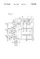
- FIG. 1is a block diagram illustrating an apparatus for producing a compound semiconductor device in accordance with a first embodiment of the present invention.
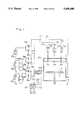
- FIG. 2is a block diagram illustrating an apparatus for producing a compound semiconductor device in accordance with a second embodiment of the present invention.
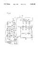
- FIG. 3is a block diagram illustrating an apparatus for producing a compound semiconductor device in accordance with a third embodiment of the present invention.
- FIG. 4is a block diagram illustrating an apparatus for producing a compound semiconductor device in accordance with a fourth embodiment of the present invention.
- FIG. 5is a block diagram illustrating an apparatus for producing a compound semiconductor device in accordance with a fifth embodiment of the present invention.
- FIG. 6is a block diagram illustrating an apparatus for producing a compound semiconductor device in accordance with a sixth embodiment of the present invention.
- FIG. 7is a block diagram illustrating an apparatus for producing a compound semiconductor device in accordance with a seventh embodiment of the present invention.
- FIG. 8is a block diagram illustrating a prior art apparatus for producing a compound semiconductor device.
- FIG. 9is a block diagram illustrating a prior art apparatus for producing a compound semiconductor device.
- FIG. 10is a block diagram illustrating a prior art apparatus for producing a compound semiconductor device.
- FIG. 11is a block diagram illustrating a prior art container of a metal organic material.
- FIG. 12is a block diagram illustrating a prior art container of a metal organic material.
- FIG. 13is a block diagram illustrating a container for a metal organic material in accordance with an eighth embodiment of the present invention.
- FIG. 14is a block diagram illustrating a container for a metal organic material in accordance with a ninth embodiment of the present invention.
- FIG. 1is a block diagram illustrating an apparatus for producing a compound semiconductor device in accordance with a first embodiment of the present invention.
- the same reference numerals as those of FIGS. 8 and 9designate the same or corresponding parts.
- desired material gas floware obtained by passing the carrier gas, H 2 , of which the flow rate is controlled by the material gas supplying MFCs 10a and 10b, through material liquids. While the material gases produced in the bubbling apparatus 18a and 18b and a material gas introduced through the MFC 10c enter the gas mixing pipe 12 via shut-off valves 20a to 20c and material gas supply pipes 11a to 11c, these gases also enter a by-pass pipe 25 via shut-off valves 19a to 19c.
- Hydrogenas a carrier gas, has a flow rate controlled by MFCs 23 and 24 and is constantly supplied to the gas mixing pipe 12 and the by-pass pipe 25.
- An end of the by-pass pipe 25is connected to the exhaust outlet 8 of the reaction tube 3.
- An end of the gas mixing pipe 12is branched into the three gas distributing pipes 13a to 13c, which are respectively connected to the gas supply inlets 6a to 6c via the reactive gas adjusting MFCs 14a to 14c.
- a control circuit 22controls the reactive gas adjusting MFCs 14a to 14c so that the output from the pressure gauge 21 installed to the gas mixing pipe 12 may be constant.
- a mesh 28is provided to smooth the flow of the mixed gas coming out of the gas supply inlets 6a to 6c.
- Trimethylgallium (Ga(CH 3 ) 3 )is generated from the bubbling apparatus 18a and trimethylaluminium (Al(CH 3 ) 3 ) is generated from the bubbling apparatus 18b.
- arsine (ASH 3 )is supplied from a bomb and is introduced to the MFC 10c with carrier gas (H 2 ).
- the wafers 2 where crystal growth is to be carried out thereonare deposited on the susceptor l in the reaction tube 3. Consecutively, with the shut-off valves 20a to 20c closed and the shut-off valves 19a to 19c opened, predetermined flow rates of the carrier gas H 2 are supplied from the MFCs 23 and 24 so that the pressure in the gas mixing pipe 12 is equal to that in the by-pass pipe 25.
- the shut-off valves 20a and 20care opened and trimethylgallium and arsine are introduced into the gas mixing pipe 12.
- the mixed material gasgoes through the gas distributing pipes 13a to 13c and the flow rate of the mixed material gas is adjusted by the MFCs 14a to 14c.
- the gasesare supplied to the reaction tube 3 via the gas supply inlets 6a to 6c.
- the control circuit 22controls the MFCs, so that the flow rates of the reactive gases supplied to the gas mixing pipe 12 by the carrier gas flowing through the MFCs 10a, 10c and 23, may be basically equal to the flow rates in the MFCs 14a to 14c connected to the gas distributing pipes 13a to 13c.
- the mixed material gasis retarded in the gas mixing pipe 12 and the pressure in the pipe 12 is increased, which is detected by the pressure gauge 21.
- the circuit 22increases the respective flow rates of the material gases flowing in the MFCs 14a to 14c in accordance the increase in the pressure. As a result, the increased pressure is lowered, resulting in a constant pressure detected at the pressure gauge 21.
- the control circuit 22reduces the respective flow rates of the material gases in the MFCs 14a to 14c, resulting in a constant pressure in the gas mixing pipe 12.
- a GaAs crystalline filmis grown on the surface of the wafers 2 supported on the susceptor 1 by the mixed material gas which is supplied as described above. Consecutively, so as to laminate an AlGaAs crystalline layer on the GaAs layer, by closing the shut-off valves 20a and 19b and opening the shut-off valves 19a and 20b, the supply of trimethylgallium stops and trimethylaluminium is supplied to the reaction tube 3.
- the carrier gasis constantly supplied to the by-pass pipe 25 so that its internal pressure is equal to that of the gas mixing pipe 12, pressure fluctuation in the gas mixing pipe 12 is decreased in switching the gases to suppress the change of the flow rates of the gases.
- a laminated filmthat has a sharp change in crystalline composition at an interface between the GaAs layer and the AlGaAs layer, is obtained.
- the reactive gas adjusting MFCs 14a to 14cby controlling the reactive gas adjusting MFCs 14a to 14c with the control circuit 22 so that the pressure in the gas mixing pipe 12 is constant, even when there are differences in precision of the MFCs 10a to 10c and 23 and the reactive gas adjusting MFCs 14a to 14c, the mixed material gas is not retarded in the gas mixing pipe 12 and further, the supply of the gas does not prevent as in the prior art apparatus, obtaining a crystalline film of a uniform thickness.
- an increased pressure in the gas mixing pipeis lowered, preventing the gas from being retarded between the MFCs.
- an end of a reactive gas by-pass pipe 27is connected to the gas mixing pipe 12 in the vicinity of the gas distributing pipes 13a to 13c.
- a by-pass gas adjusting MFC 26is disposed in the by-pass pipe 27 that is connected to the by-pass pipe 25.
- a control circuit 22acontrols the flow rate of the by-pass gas adjusting MFC 26, receiving an output from the pressure gauge 21 disposed in the gas mixing pipe 12.
- the operations of the respective valves in conducting crystal growthare the same as those of the first embodiment.
- descriptionis given of a case where the gas is retarded due to differences in precision of the MFCs 10a to 10c and 23 and the MFCs 14a to 14c.
- the mixed material gasis retarded in the gas mixing pipe 12 and the pressure in the pipe 12 is increased, which is detected by the pressure gauge 21.
- the circuit 22aincreases the flow rate of the material gas flowing in the by-pass gas adjusting MFC 26 in accordance with the increase in the pressure.
- the reactive gas equivalent to the excessive pressureflows into the by-pass pipe 25 and the increased pressure in the gas mixing pipe 12 is lowered, resulting in a constant pressure detected at the pressure gauge 21.
- any increased pressure in the gas mixing pipeis lowered, preventing the gas from being retarded between the MFCs.
- a control circuit 22bcontrols the MFC 23 so that the detected pressure may be constant, receiving an output from the pressure gauge 21 placed in the gas mixing pipe 12.
- the control circuit 22bdecreases the flow rate of the carrier gas flowing in the MFC 23 connected to the gas mixing pipe 12, which constantly supplies carrier gas H 2 , according to the increased pressure.
- the control circuit 22bincreases the flow rate flowing in the MFC 23 so that the pressure in the gas mixing pipe 12 is increased to be a predetermined pressure.
- MFCs 23a and 23bare employed so as to supply the carrier gas to the gas mixing pipe 12
- two or more MFCsmay be employed and a plurality of MFCs for adjusting the flow rate of the carrier gas may be employed.
- a control circuit 22ccontrols the MFCs 10a to 10c, receiving an output from the pressure gauge 21.
- the control circuit 22cdecreases the flow rates in the MFCs 10a to 10c according to the increased pressure, which constantly adjusts the flow rates of carrier gas H 2 for generating the respective material gases.
- the increased pressure in the gas mixing pipe 12is lowered, producing a constant pressure detected by the pressure gauge 21.
- the control circuit 22cincreases the flow rates in the MFCs 10a to 10c so that the pressure in the gas mixing pipe 12 is increased to be a predetermined pressure.
- MFCs 40a and 40b for supplying a V-group gasi.e., a gaseous source of a group V element
- a V-group gasi.e., a gaseous source of a group V element
- MFCs 41a and 41brespectively supply a dopant impurity gas to the reaction tube 3 via impurity gas supply pipes 43a and 43b which are separated from each other.
- An MFC 42supplies the carrier gas H 2 to a gas mixing pipe 12b and the impurity gas supply pipes 43a and 43b via a pipe 44.
- the bubbling apparatus 18a and 18bsupply III-group gases (trimethylgallium, trimethylaluminium) and the bubbling apparatus 18c is not used.
- a gas mixing pipe 12afor supplying the III-group gases to the reaction tube 3 and the gas mixing pipe 12b for supplying the V-group gas (AsH 3 ), and further there are separate impurity gas supply pipes 43a and 43b and gas mixing pipes 12a and 12b.
- the carrier gas H 2is introduced into the bubbling apparatus 10a to 10c filled with the III-group material, which are disposed before the gas mixing pipe 12a, the material is vaporized, and introduced into the reaction tube through the gas mixing pipe 12a.
- the V-group gas in a bombis mixed with H 2 gas sent from the pipe 44 inside the gas mixing pipe 12b and introduced into the reaction tube 3.
- the III-group gas and the V-group gasare respectively introduced through gas distributing pipes 45a to 45c and 46a to 46c into which ends of the gas mixing pipes 12a and 12b are respectively branched and a crystalline layer is grown on the surface of the wafer 2.
- the layer thickness of the crystalmainly depends on the layer thickness distribution of the boundary-layer and the concentration distribution of the III-group material in the boundary-layer.
- the compositiondepends on the concentration distribution of the V-group material in the boundary-layer and its decomposition coefficient. Therefore, the distribution ratio of the III-group gas and that of the V-group gas are adjusted resulting in a crystalline film with uniformity in layer thickness and composition.
- the concentration of the III-group gasis made uniform by adjusting the distribution ratios of the III-group gas with needle valves 29 disposed in the gas distributing pipes 45a to 45c downstream of the gas mixing pipe 12a
- the concentration of the V-group gasis made uniform by adjusting the distribution ratios of the V-group gas with the needle valves 29 disposed in the gas distributing pipes 46a to 46c downstream of the gas mixing pipe 12b.
- the III-group gas and the V-group gasare adjusted respectively to have a predetermined gas flow rate and a predetermined distribution ratio, resulting in uniformity in thickness and composition of the crystalline layer.
- the impurity concentration in the crystaldepends on the impurity concentration in the gas phase and the ratio of concentration between the impurity and the elements constituting the crystal in the gas phase, and in order to make the impurity concentration in the crystal uniform, it is necessary to control the impurity concentration in the gas phase and the distribution of the partial pressure for each impurity.
- the impurity concentration in the crystaldepends on the proportion of SiH 4 gas to III-group gas in the gas phase, i.e., SiH 4 /III-group gas ratio. Therefore, in order to obtain the uniformity of Si concentration in the crystal, the distribution ratios of the SiH 4 gas in distributing pipes 50a to 50c for supplying SiH 4 are adjusted so that the distribution of the SiH 4 /III-group gas ratio is uniform.
- the impurity concentration in the crystaldepends on the proportion of H 2 S or H 2 Se gas to V-group gas in the gas phase, i.e., H 2 S/V-group or H 2 Se/V-group gas ratio.
- the distribution ratios of the H 2 S gas or H 2 Se gas in distributing pipes 51a to 51c for supplying H 2 S or H 2 Seare adjusted so that the distribution of the proportion of H 2 S/V-group or H 2 Se/V-group gas ratio is uniform.
- the III-group gas and the V-group gasare respectively introduced into the reaction tube 3 using the gas mixing pipes 12a and 12b which are separated from each other, the distribution ratios of respective gases are set considering the decomposition coefficient of the crystal material. Therefore, even when the crystal growth is carried out on a number of large sized substrates, for example, 6 or more 2-inch wafers, or 3 or more 3-inch wafers, employing a susceptor of a diameter of 20cm and more, a crystal having sufficient uniformity on the entire substrate in its layer thickness and its composition is obtained.
- the impurity gas supply pipes 43a and 43bare separate from the gas mixing pipes 12a and 12b, the concentration in the gas phase and the concentration ratio between the impurity gas and the reactive gas introduced from the gas mixing pipes 12a and 12b are easily controlled, resulting in the crystal having the uniformity in impurity concentration.
- a gate mechanismsuch as electromagnetic valve or needle valve may be employed in place of the MFC 26.
- reference numeral 56designates a first mass flow controller (MFC), a first flow rate control gauge.
- MFCmass flow controller
- a second MFC 59to be a second flow rate control gauge, is disposed downstream of a second gas exhausting pipe 58.
- a carrier gas flowfor example H 2 at 30 cc per minute
- a carrier gas flowfor example H 2 at 30 cc per minute
- H 2at 30 cc per minute
- a carrier gas saturated with vapor from the metal organic material 54i.e., a material gas
- the flow rate of the second MFC 59is set at 3 cc/min and the pressure of a pressure controller 57 is set at 760 torr.
- the material gas at 3 cc/minstably flows downstream of the second MFC 59, while the material gas at 27 cc/min stably flows to the downstream of the pressure controller 57.
- the second gas exhausting pipe 58is disposed at the cylinder 53 and a desired small amount of material gas is obtained from the second gas exhausting pipe 58. Therefore, even when a small amount of reactive gas is to be obtained, the continuous bubbles 55 are generated from the sufficient amount of carrier gas, thereby obtaining the material gas having a constant amount of vapor.
- a carrier gas introducing pipe 51bis inserted into a carrier gas introducing pipe 60 having a sliding mechanism, and a gas exhausting pipe 52 is inserted into a gas exhausting pipe 61 having a sliding mechanism.
- These pipes 60 and 61are fixed to a partition plate 63 attached to a hollow float 62 so that respective ends of the pipes 60 and 61 maintain heights of h1 and h2 from the liquid level by a liquid level maintaining mechanism comprising the float 62 and the partition plate 63. It is preferred to use a material for the hollow float 62, which is not corroded by the metal organic material 54.
- H 2 gasdoes not pass through the metal organic material 54, takes in saturated vapor at the surface of the metal organic material 54 in an equilibrium state without generating bubbles, and is exhausted from the cylinder 53 through the gas exhausting pipe 61 having the sliding mechanism and the gas exhausting pipe 52.
- the distance between the hollow float 62 which floats on the liquid level of the metal organic material 54 and the partition plate 63is always constant, the height h2 between the gas exhausting pipe 61 having the sliding mechanism and the liquid level is kept constant, and the amount of vapor from the metal organic material taken in into the gas exhausting pipe 61 does not vary even with the consumption of the material, whereby a desired amount of material gas is stably taken out.
- the gas exhausting pipe 61 having the sliding mechanismwhich is fixed by hollow float 62 on the liquid level of the metal organic material 54, is provided at an end of the gas exhausting pipe 52, regardless of a change of the liquid level with the consumption of the material, the distance between the end of the pipe 61 and the liquid level of the metal organic material 54 is always kept at height h2, thereby producing the material gas having a constant amount of vapor from the material.
- pressure controller 57is provided downstream of the first gas exhausting pipe 52 in the above-described eighth embodiment, a mass flow controller as well as a mass flow adjusting gauge such as needle valve can be used.
- an apparatus for producing a semiconductor device in accordance with the present inventionby controlling a first or a second flow rate adjusting means of a gas mixing pipe or a carrier gas adjusting means so that the detected pressure in the gas mixing pipe is constant, exhausting a portion of a reactive gas from the gas mixing pipe outside, retardation of the gases between the first and the second flow rate adjusting means is prevented, increasing uniformity in the layer thickness of the crystals.
- the distribution ratio of each material gasmay be set considering the decomposition coefficients of respective materials, thereby resulting in a crystal superior in uniformity in thickness and composition. This improves the characteristics of the semiconductor device, production yield and mass production.
- a pipe for exhausting material gasis employed.
- a distance between an end of the material gas exhausting pipe and the liquid level of the metal organic materialis kept constant, so that quite a small amount of metal organic material steam is stably supplied.
- the speed of crystal growthis slowed down, and crystal growth control at a level of atomic layers is achieved and a minute mixed crystal ratio, i.e., crystal composition, is easily controlled in the crystal growth of mixed system crystal, for example, AlGaAs.
Landscapes
- Chemical & Material Sciences (AREA)
- Engineering & Computer Science (AREA)
- Materials Engineering (AREA)
- Chemical Kinetics & Catalysis (AREA)
- Organic Chemistry (AREA)
- Metallurgy (AREA)
- General Chemical & Material Sciences (AREA)
- Microelectronics & Electronic Packaging (AREA)
- Condensed Matter Physics & Semiconductors (AREA)
- Power Engineering (AREA)
- General Physics & Mathematics (AREA)
- Physics & Mathematics (AREA)
- Computer Hardware Design (AREA)
- Manufacturing & Machinery (AREA)
- Mechanical Engineering (AREA)
- Crystallography & Structural Chemistry (AREA)
- Crystals, And After-Treatments Of Crystals (AREA)
Abstract
Description
The present invention relates to a compound semiconductor crystal growth apparatus utilizing a vapor phase growth method and, more particularly, to an improvement in a mechanism for supplying material gas to a reaction tube.
FIG. 8 is a block diagram illustrating a prior art compound semiconductor crystal growth apparatus for forming a thin film on a plurality of wafers by a low pressure chemical vapor deposition. More specifically, in this growth apparatus a chemical reaction of material gases under reduced pressure deposits a solid on the wafer.
More particularly, as illustrated in FIG. 8, asusceptor 1 holding a plurality ofwafers 2 is placed in areaction tube 3 having a cylindrical shape and, after both ends of thereaction tube 3 are closed withlids 4 and 5, a reactive gas (a mixture of material gases) is supplied to thereaction tube 3 viagas supply inlets 6a to 6c. Then, in a state where the pressure in thereaction tube 3 is reduced via anexhaust outlet 8 by an.exhaust pump 9, the inside of thereaction tube 3 is heated to a prescribed temperature by applying an electric current to afurnace 7, to deposit a crystalline film on thewafers 2 according to the chemical reaction of the material gas. Here, the flow rate of the material gas required for crystal growth, is controlled by mass flow controllers (hereinafter referred to as MFC) for supplyingmaterial gas 10a to 10c, and respective gases are introduced through materialgas supply pipes 11a to 11c into agas mixing pipe 12 for mixing those gases. The material gas mixed therein is introduced into thereaction tube 3 throughgas distributing pipes 13a to 13c, in order to equalize the thickness, or control the composition of the crystal grown in thereaction tube 3.
By employing the above-described growth apparatus, gas distribution in the reaction tube is improved to a greater extent than that in a case where the reactive gas is provided via a single gas supply inlet from only one end of the reaction tube. However, the flow rates of the mixed material gas flowing through the respective gas distributing pipes are not made equal to each other by branching the mixed gas supply pipe into plural pipes and do not result in a thin film having a high quality.
In a low pressure chemical vapor deposition apparatus illustrated in FIG. 9, which is disclosed in Japanese Published Utility Model Application No. Hei.2-33260, according to an output voltage from a mass flow meter (hereinafter referred to as MFM) 15 placed in thegas mixing pipe 12, which output voltage is input to agas controlling circuit 16, i.e., according to the flow rate of the mixed material gas flowing in theMFM 15, the flow rates of the mixed material gas flowing in therespective MFCs gas distributing pipes respective MFCs 14a to 14c are kept at values which are preset at settingappliances 17a to 17c, controlled by thegas controlling circuit 16. As a result, the flow rates of the mixed material gas flowing through the respectivegas distributing pipes reaction tube 3 equalized.
When, between the materialgas supplying MFCs 10a to 10c and theMFCs 14a to 14c, a difference in precision occurs due to errors in manufacture, deterioration over time or the like of the MFCs occurs, i.e., when though thegas controlling circuit 16 makes the flow rates of material gases flowing in theMFCs 14a to 14c equal to those flowing in theMFCs 10a to 10c, the total flow rates of theformer MFCs 14a to 14c are smaller than those of thelatter MFCs 10a to 10c. As a result, the mixed material gas is retarded in thegas mixing pipe 12 located between theMFCs 14a to 14c and theMFCs 10a to 10c, lowering the flow rate of the mixed material gas flowing in theMFM 15. In this structure, however, the flow rates of the reactive gas flowing in theMFCs 14a to 14c are lowered with a decrease in the flow rate of the material gas measured in theMFM 15, and further more material gases are retarded in thegas mixing pipe 12, further lowering the flow rates of the material gases, resulting in a vicious circle.
In the prior art compound semiconductor crystal growth apparatus constructed as described above, the material gas is retarded in the gas mixing pipe between the MFCs disposed respectively at prior and latter stage of the gas mixing pipe, due to errors in manufacture, deterioration over time or the like of the MFCs, and in the worst case, the supply of the mixed material gas stops.
FIG. 10 is a block diagram illustrating a prior art crystal growth apparatus, which is disclosed in Japanese Patent Application No. Hei.1-140712. In the figure,wafers 2 are disposed on asusceptor 31 having arotation shaft 30. Flowrate variable valves 32a to 32d are disposed ingas distributing pipes 13. Prescribed material liquids are included inbubbling apparatus 33a to 33c and H2 gas as carrier gas is passed therethrough to generate desired material gases. Shut-offvalves 35a to 35d are used for maintenance.
In this apparatus, after the material gases generated in thebubbling apparatus 33a to 33c are mixed in agas mixing pipe 12, the ratio of flow quantities (distribution ratio) of the mixed material gases flowing through thegas distributing pipes 13 are controlled by the flowrate variable valves 32a to 32d having a prescribed degree of opening, and the mixed material gas is introduced into thereaction tube 3. The material gases introduced into thereaction tube 3 as described above react on the surface or in the vicinity of thewafers 2, growing desired crystals on thewafers 2. Thus, in this apparatus, the uniformity in the layer thickness and composition of the crystal layer grown on thewafer 2 is increased by adjusting the flow rates of the gases flowing through thegas distributing pipes 13. According to this prior art apparatus, however, the inherent nature of each material is not considered. Therefore, in processing a number of large sized wafers, it was difficult to control the uniformity of the layer thickness, the composition and the impurity addition amount of the grown crystal layer sufficiently over the whole surface of the wafer.
In the apparatus illustrated in FIG. 10, the material gases are generated using bubbling apparatus (containers of metal organic material). However, there is a problem that a small amount of metal organic material gas is not stably supplied in the conventional bubbling apparatus.
More particularly, as illustrated in FIG. 11, in conventional bubbling apparatus, by supplying a specific flow rate of a carrier gas, for example, H2, to a material container 53 (hereinafter also referred to as cylinder) from apipe 51 for introducing carrier gas through anMFC 56 and passing the carrier gas through metalorganic material 54, bubbles 55 are generated, and a material gas saturated with vapor from the metal organic material is exhausted from apipe 52 for exhausting gas. At this time, by setting a control pressure of apressure control gauge 57 placed in thegas exhausting pipe 52 at a prescribed value, a prescribed amount of material gas having a constant vapor pressure is obtained. However, in order to take out a small amount of material gas, a small amount of carrier gas must be introduced into the metal organic material. The bubbles generated at that time are not continuous bubbles but are intermittent and unstable because the quantity of introduced carrier gas is too small. Therefore, the amount of vapor of the material gas exhausted from thegas exhausting pipe 52 is also unstable, whereby the desired vapor flow from the metal organic material is not produced.
So as to solve the above-described problems, as illustrated in FIG. 12, an end of a carriergas introducing pipe 51a is not immersed in the metalorganic material 54. In this apparatus, a carrier gas supplied to thecylinder 53 does not generate any bubbles, takes in a saturated vapor at the surface of the metalorganic material 54 in an equilibrium state, and is exhausted from thegas exhausting pipe 52 as a material gas. However, in this apparatus, as the metal organic material is consumed, the distance between thegas exhausting pipe 52 and the liquid level of the metalorganic material 54 is varied. Therefore, the amount of vapor of the material gas taken in thegas exhausting pipe 52 varies with the consumption of the material, whereby a desired flow of material gas is not stably produced.
It is an object of the present invention to control regularly the flow rate of a mixed material gas even when there is difference in precision due to errors in manufacture and deterioration over time of MFCs between the material gas supplying MFCs and the reactive gas adjusting MFCs.
It is another object of the present invention to provide an apparatus for producing a compound semiconductor device capable of obtaining the uniformity in layer thickness, composition, and impurity concentration in a crystalline layer grown on the entire surface of the wafer.
It is still another object of the present invention to provide a container of metal organic material capable of stably supplying a small amount of material gas.
Other objects and advantages of the present invention will become apparent from the detailed description given hereinafter; it should be understood, however, that the detailed description and specific embodiment are given by way of illustration only, since various changes and modifications within the spirit and scope of the invention will become apparent to the those skilled in the art from this detailed description.
According to a first aspect of the present invention, an apparatus for producing a compound semiconductor device includes first flow rate adjusting means, a gas mixing pipe for mixing the material gases having controlled flow rates, a plurality of gas distributing pipes connected to an end of the gas mixing pipe, second flow rate adjusting means for adjusting the flow of material gas flowing through the gas distributing pipes and for supplying the material gases to a reaction tube, means for detecting pressure in the gas mixing pipe and a control means for, upon receipt of an output from the pressure detecting means, controlling the second flow rate adjusting means to keep the pressure in the gas mixing pipe at a constant value. Therefore, retardation of the material gas between the first and the second flow rate adjusting means is prevented.
According to a second aspect of the present invention, the above-described apparatus for producing a compound semiconductor device further includes a reactive gas by-pass pipe for branching and exhausting a reactive gas from the gas mixing pipe, a by-pass pipe flow rate adjusting means for controlling the reactive gas flowing through the reactive gas by-pass pipe and a control means for, upon receipt of an output from the pressure detecting means, controlling the by-pass pipe flow rate adjusting means to keep the pressure in the gas mixing pipe at a constant value. Therefore, retardation of the material gas between the first and the second flow rate adjusting means is prevented.
According to a third aspect of the present invention, the above-described apparatus for producing a compound semiconductor device further includes a control means for, upon receipt of an output from the pressure detecting means, controlling the first flow rate adjusting means to keep the pressure in the gas mixing pipe at a constant value. Therefore, retardation of the material gas between the first and the second flow rate adjusting means is prevented.
According to a fourth aspect of the present invention, the above-described apparatus for producing a compound semiconductor device further includes a control means for, upon receipt of an output from the pressure detecting means, controlling the carrier gas flow rate adjusting means to keep the pressure in the gas mixing pipe at a constant value. Therefore, retardation of the material gas between the first and the second flow rate adjusting means is prevented.
According to a fifth aspect of the present invention, the above-described apparatus for producing a compound semiconductor device further includes a by-pass pipe for exhausting a carrier gas from the gas mixing pipe. Therefore, in addition to the effect of the above-described aspects, no change of the supply flow rate of the material gas occurs, suppressing a change in the composition of the crystal.
According to a sixth aspect of the present invention, an apparatus for producing a compound semiconductor device in which material gases including a component element of a compound semiconductor crystal are introduced into a reaction tube and growth of a compound semiconductor occurs out on wafers disposed in the reaction tube, includes material gas supply pipes which are separated from each other in every group of the component element included in the material gases, and flow rate adjusting means for adjusting flow rates of the material gases flowing through the material gas supply pipes. The apparatus for producing a compound semiconductor device further includes impurity gas supply pipes separated from the material gas supply pipes. Therefore, the distribution ratio of each material gas is set considering the decomposition coefficient of the material, and the impurity concentration in the gas phase and the distribution ratio are controlled.
According to a seventh aspect of the present invention, an apparatus which, containing a liquefied metal organic material, receives a carrier gas and exhausts a material gas produced by the carrier gas saturated with vapor from the metal organic material includes a container containing the liquefied metal organic material, a pipe for introducing a carrier gas, which, having its end immersed in the metal organic material, supplies the carrier gas to the container through a carrier gas flow rate controller, a first pipe for exhausting material gas, which, having its end not in contact with a liquid level of the metal organic material, exhausts a large amount of material gas downstream through a first material gas flow rate controller for controlling one of pressure and flow quantity of the material gas, and a second pipe for exhausting material gas, which, having its end not in contact with the liquid level of the metal organic material, exhausts a small amount of material gas to the downstream through a second material gas flow rate controller. Therefore, a small amount of vapor from the metal organic material is stably obtained due to continuous bubbles.
According to an eighth embodiment of the present invention, the above-described apparatus containing a liquefied metal organic material further includes a pipe for introducing carrier gas, which supplies the carrier gas to the container through a first flow rate controller, a pipe for exhausting material gas, which includes a second flow rate controller at the downstream end thereof, and patching pipes which are provided at respective ends of the carrier gas introducing pipe and the material gas exhausting pipe so as to slide flexibly and having ends floating over a liquid level of the metal organic material while keeping a constant space therebetween so that the ends are not in contact with the liquid level. Therefore, even if the liquid level is lowered as the material is consumed, the distance between the material gas exhausting pipe and the liquid level is kept constant.
FIG. 1 is a block diagram illustrating an apparatus for producing a compound semiconductor device in accordance with a first embodiment of the present invention.
FIG. 2 is a block diagram illustrating an apparatus for producing a compound semiconductor device in accordance with a second embodiment of the present invention.
FIG. 3 is a block diagram illustrating an apparatus for producing a compound semiconductor device in accordance with a third embodiment of the present invention.
FIG. 4 is a block diagram illustrating an apparatus for producing a compound semiconductor device in accordance with a fourth embodiment of the present invention.
FIG. 5 is a block diagram illustrating an apparatus for producing a compound semiconductor device in accordance with a fifth embodiment of the present invention.
FIG. 6 is a block diagram illustrating an apparatus for producing a compound semiconductor device in accordance with a sixth embodiment of the present invention.
FIG. 7 is a block diagram illustrating an apparatus for producing a compound semiconductor device in accordance with a seventh embodiment of the present invention.
FIG. 8 is a block diagram illustrating a prior art apparatus for producing a compound semiconductor device.
FIG. 9 is a block diagram illustrating a prior art apparatus for producing a compound semiconductor device.
FIG. 10 is a block diagram illustrating a prior art apparatus for producing a compound semiconductor device.
FIG. 11 is a block diagram illustrating a prior art container of a metal organic material.
FIG. 12 is a block diagram illustrating a prior art container of a metal organic material.
FIG. 13 is a block diagram illustrating a container for a metal organic material in accordance with an eighth embodiment of the present invention.
FIG. 14 is a block diagram illustrating a container for a metal organic material in accordance with a ninth embodiment of the present invention.
FIG. 1 is a block diagram illustrating an apparatus for producing a compound semiconductor device in accordance with a first embodiment of the present invention. In the figure, the same reference numerals as those of FIGS. 8 and 9 designate the same or corresponding parts. In bubblingapparatus gas supplying MFCs apparatus MFC 10c enter thegas mixing pipe 12 via shut-offvalves 20a to 20c and materialgas supply pipes 11a to 11c, these gases also enter a by-pass pipe 25 via shut-offvalves 19a to 19c. Hydrogen, as a carrier gas, has a flow rate controlled byMFCs gas mixing pipe 12 and the by-pass pipe 25. An end of the by-pass pipe 25 is connected to theexhaust outlet 8 of thereaction tube 3. An end of thegas mixing pipe 12 is branched into the threegas distributing pipes 13a to 13c, which are respectively connected to thegas supply inlets 6a to 6c via the reactivegas adjusting MFCs 14a to 14c. Acontrol circuit 22 controls the reactivegas adjusting MFCs 14a to 14c so that the output from thepressure gauge 21 installed to thegas mixing pipe 12 may be constant. Amesh 28 is provided to smooth the flow of the mixed gas coming out of thegas supply inlets 6a to 6c.
Next, description is given of the operations.
Here, a case will be described when a GaAs layer and an AlGaAs layer are successively laminated on thewafers 2. Trimethylgallium (Ga(CH3)3) is generated from the bubblingapparatus 18a and trimethylaluminium (Al(CH3)3) is generated from the bubblingapparatus 18b. Here, arsine (ASH3) is supplied from a bomb and is introduced to theMFC 10c with carrier gas (H2).
First, thewafers 2 where crystal growth is to be carried out thereon, are deposited on the susceptor l in thereaction tube 3. Consecutively, with the shut-offvalves 20a to 20c closed and the shut-offvalves 19a to 19c opened, predetermined flow rates of the carrier gas H2 are supplied from theMFCs gas mixing pipe 12 is equal to that in the by-pass pipe 25.
Secondly, with the shut-offvalves valves gas mixing pipe 12. The mixed material gas goes through thegas distributing pipes 13a to 13c and the flow rate of the mixed material gas is adjusted by theMFCs 14a to 14c. Then, the gases are supplied to thereaction tube 3 via thegas supply inlets 6a to 6c. Here, thecontrol circuit 22 controls the MFCs, so that the flow rates of the reactive gases supplied to thegas mixing pipe 12 by the carrier gas flowing through theMFCs MFCs 14a to 14c connected to thegas distributing pipes 13a to 13c. However, when the actual flow rates are not equal to the designed flow rates due to differences in the precision and deterioration with time of theMFCs MFCs 14a to 14c, so an adjustment is required in order to equalize these flow rates.
For example, when the actual flow rate of the reactive gas supplied by theMFCs gas mixing pipe 12 and the pressure in thepipe 12 is increased, which is detected by thepressure gauge 21. Then, when the detected result is input into thecontrol circuit 22, thecircuit 22 increases the respective flow rates of the material gases flowing in theMFCs 14a to 14c in accordance the increase in the pressure. As a result, the increased pressure is lowered, resulting in a constant pressure detected at thepressure gauge 21.
On the other hand, when the actual total flow rates of the reactive gases flowing through the MFCs 14a to 14c are larger than the actual flow rate of the reactive gas supplied by theMFCs pressure gauge 21 is reduced, thecontrol circuit 22 reduces the respective flow rates of the material gases in theMFCs 14a to 14c, resulting in a constant pressure in thegas mixing pipe 12.
A GaAs crystalline film is grown on the surface of thewafers 2 supported on thesusceptor 1 by the mixed material gas which is supplied as described above. Consecutively, so as to laminate an AlGaAs crystalline layer on the GaAs layer, by closing the shut-offvalves valves reaction tube 3. Here, since the carrier gas is constantly supplied to the by-pass pipe 25 so that its internal pressure is equal to that of thegas mixing pipe 12, pressure fluctuation in thegas mixing pipe 12 is decreased in switching the gases to suppress the change of the flow rates of the gases. As constructed as described above, a laminated film that has a sharp change in crystalline composition at an interface between the GaAs layer and the AlGaAs layer, is obtained.
Thus, in this first embodiment, by controlling the reactivegas adjusting MFCs 14a to 14c with thecontrol circuit 22 so that the pressure in thegas mixing pipe 12 is constant, even when there are differences in precision of the MFCs 10a to 10c and 23 and the reactivegas adjusting MFCs 14a to 14c, the mixed material gas is not retarded in thegas mixing pipe 12 and further, the supply of the gas does not prevent as in the prior art apparatus, obtaining a crystalline film of a uniform thickness.
Description will be given of an apparatus for producing a compound semiconductor device in accordance with a second embodiment of the present invention.
In this second embodiment, by letting a portion of the gases out of the gas mixing pipe to the by-pass pipe, an increased pressure in the gas mixing pipe is lowered, preventing the gas from being retarded between the MFCs. More particularly, in FIG. 2, an end of a reactive gas by-pass pipe 27 is connected to thegas mixing pipe 12 in the vicinity of thegas distributing pipes 13a to 13c. A by-passgas adjusting MFC 26 is disposed in the by-pass pipe 27 that is connected to the by-pass pipe 25. Acontrol circuit 22a controls the flow rate of the by-passgas adjusting MFC 26, receiving an output from thepressure gauge 21 disposed in thegas mixing pipe 12.
Next, description is given of the operations.
The operations of the respective valves in conducting crystal growth are the same as those of the first embodiment. Here, description is given of a case where the gas is retarded due to differences in precision of the MFCs 10a to 10c and 23 and theMFCs 14a to 14c. Similarly to the first embodiment, when the actual flow rate of the reactive gas supplied by theMFCs gas mixing pipe 12 and the pressure in thepipe 12 is increased, which is detected by thepressure gauge 21. Then, when the detected result is input into thecontrol circuit 22a, thecircuit 22a increases the flow rate of the material gas flowing in the by-passgas adjusting MFC 26 in accordance with the increase in the pressure. As a result, the reactive gas equivalent to the excessive pressure flows into the by-pass pipe 25 and the increased pressure in thegas mixing pipe 12 is lowered, resulting in a constant pressure detected at thepressure gauge 21.
According to this embodiment as described above, by including the reactive gas by-pass pipe 27, and by controlling the by-passgas adjusting MFC 26 disposed in the reactive gas by-pass pipe 27 with thecontrol circuit 22a, so that the pressure detected at thepressure gauge 21 is constant, even if there are differences the precision of the MFCs, the gas is not retarded. Any MFCs, because the excessive reactive gas flows into the by-pass pipe 25 through the reactive gas by-pass pipe 27.
Description will be given of an apparatus for producing a compound semiconductor device in accordance with a third embodiment of the present invention.
While in the second embodiment the reactive gas by-pass pipe 27 is connected to thegas mixing pipe 12 in the vicinity of thegas distributing pipes 13a to 13c, as illustrated in FIG. 3, in this third embodiment an end of a carrier gas by-pass pipe 27a is connected to thegas mixing pipe 12 in the vicinity of theMFC 23 supplying the carrier gas. In this construction, when the by-passgas adjusting MFC 26 disposed in the way of the carrier gas by-pass pipe 27a is adjusting the flow rate of the gas, only the carrier gas is exhausted to theexhaust outlet 8. This makes no change in the supply flow rates of the material gases to thereaction tube 3, suppressing any change in the composition of a growing crystal.
Description will be given of an apparatus for producing a compound semiconductor device in accordance with a forth embodiment of the present invention.
In this fourth embodiment, by controlling the MFC connected to the gas mixing pipe, any increased pressure in the gas mixing pipe is lowered, preventing the gas from being retarded between the MFCs. More particularly, in FIG. 4, acontrol circuit 22b controls theMFC 23 so that the detected pressure may be constant, receiving an output from thepressure gauge 21 placed in thegas mixing pipe 12.
Next, description is given of the operations.
Similarly to the above-described embodiments, when the actual flow rates of the reactive gas supplied by theMFCs gas mixing pipe 12 and the pressure in thepipe 12 is increased, which is detected by thepressure gauge 21. Then, when the detected result is input into thecontrol circuit 22b, thecontrol circuit 22b decreases the flow rate of the carrier gas flowing in theMFC 23 connected to thegas mixing pipe 12, which constantly supplies carrier gas H2, according to the increased pressure. As a result, the increased pressure in thegas mixing pipe 12 is lowered, producing a constant pressure detected by thepressure gauge 21. On the other hand, when the pressure detected by thepressure gauge 21 is smaller than the predetermined value, thecontrol circuit 22b increases the flow rate flowing in theMFC 23 so that the pressure in thegas mixing pipe 12 is increased to be a predetermined pressure.
According to this fourth embodiment as described above, with controlling theMFC 23 by thecontrol circuit 22b so that the pressure in thegas mixing pipe 12 detected by thepressure gauge 21 is constant, the material gas is not retarded between the MFCs even if there are differences in precision of the MFCs.
Description will be given of an apparatus for producing a compound semiconductor device in accordance with a fifth embodiment of the present invention.
While in the fourth embodiment the pressure in thegas mixing pipe 12 is detected and theMFC 23 is directly controlled by thecontrol circuit 22b, in this fifth embodiment illustrated in FIG. 5, a plurality ofMFCs gas mixing pipe 12, and theMFC 23b is controlled by thecontrol circuit 22b. Here, theMFC 23b, differently from the other MFCs, must have a sufficient capacity to control the supply flow rate of the carrier gas so that the pressure in thegas mixing pipe 12 may be constant when retardation occurs in thegas mixing pipe 12.
Thus, by adjusting the flow rate of the carrier gas with theMFC 23b in order to control the pressure in thegas mixing pipe 12, retardation between the MFCs is avoided with a good response to pressure changes.
While in this fifth embodiment twoMFCs gas mixing pipe 12, two or more MFCs may be employed and a plurality of MFCs for adjusting the flow rate of the carrier gas may be employed.
Description will be given of an apparatus for producing a compound semiconductor device in accordance with a sixth embodiment of the present invention.
While, in the above-described fourth and fifth embodiments, the increased pressure in thegas mixing pipe 12 is lowered by controlling the MFC supplying the carrier gas to thegas mixing pipe 12, in this embodiment, by controlling the MFCs connected to the bubbling apparatus connected to the material gas supply pipes, retardation of the gas between the MFCs is prevented. In FIG. 6, acontrol circuit 22c controls theMFCs 10a to 10c, receiving an output from thepressure gauge 21.
Next, description is given of the operations.
Similarly to the above-described embodiments, when the actual flow rate of the reactive gas supplied by theMFCs gas mixing pipe 12 and the pressure in thepipe 12 is increased, which is detected by thepressure gauge 21. Then, when the detected result is input into thecontrol circuit 22c, thecontrol circuit 22c decreases the flow rates in theMFCs 10a to 10c according to the increased pressure, which constantly adjusts the flow rates of carrier gas H2 for generating the respective material gases. As a result, the increased pressure in thegas mixing pipe 12 is lowered, producing a constant pressure detected by thepressure gauge 21. On the other hand, when the pressure detected by thepressure gauge 21 is smaller than the predetermined value, thecontrol circuit 22c increases the flow rates in theMFCs 10a to 10c so that the pressure in thegas mixing pipe 12 is increased to be a predetermined pressure.
According to this sixth embodiment as described above, by controlling theMFCs 10a to 10c with thecontrol circuit 22c while supplying carrier gas for generating the material gas, so that the pressure in thegas mixing pipe 12 detected by thepressure gauge 21 is constant, the gas is not retarded between the MFCs even if there are differences in precision between the MFCs.
Description will be given of an apparatus for producing a compound semiconductor device in accordance with a seventh embodiment of the present invention.
While gas retardation between the MFCs is solved in the above-described embodiments, uniformity in the layer thickness, composition, and impurity addition amount of a crystalline layer grown on the entire surface of the wafer is obtained in this seventh embodiment.
In FIG. 7,MFCs 40a and 40b for supplying a V-group gas, i.e., a gaseous source of a group V element, are connected to thereaction tube 3 via agas mixing pipe 12b. For example, arsine (AsH3) is supplied from a bomb 100a which is connected to the MFC 40a. MFCs 41a and 41b respectively supply a dopant impurity gas to thereaction tube 3 via impuritygas supply pipes 43a and 43b which are separated from each other. AnMFC 42 supplies the carrier gas H2 to agas mixing pipe 12b and the impuritygas supply pipes 43a and 43b via apipe 44. Here, the bubblingapparatus apparatus 18c is not used. Thus, in this seventh embodiment, there are separately provided agas mixing pipe 12a for supplying the III-group gases to thereaction tube 3 and thegas mixing pipe 12b for supplying the V-group gas (AsH3), and further there are separate impuritygas supply pipes 43a and 43b andgas mixing pipes
Description will be given of a crystal growth method performed employing the above-described apparatus.
The carrier gas H2 is introduced into the bubblingapparatus 10a to 10c filled with the III-group material, which are disposed before thegas mixing pipe 12a, the material is vaporized, and introduced into the reaction tube through thegas mixing pipe 12a. The V-group gas in a bomb is mixed with H2 gas sent from thepipe 44 inside thegas mixing pipe 12b and introduced into thereaction tube 3. Opposite the surface of thewafer 2, the III-group gas and the V-group gas are respectively introduced throughgas distributing pipes 45a to 45c and 46a to 46c into which ends of thegas mixing pipes wafer 2.
Here, in order to make the thickness and the composition uniform, it is necessary to set the respective distribution ratios for the III-group gas and the V-group gas while considering the respective decomposition coefficients of the III-group and V-group materials, respectively. The layer thickness of the crystal mainly depends on the layer thickness distribution of the boundary-layer and the concentration distribution of the III-group material in the boundary-layer. The composition depends on the concentration distribution of the V-group material in the boundary-layer and its decomposition coefficient. Therefore, the distribution ratio of the III-group gas and that of the V-group gas are adjusted resulting in a crystalline film with uniformity in layer thickness and composition.
In this apparatus, the concentration of the III-group gas is made uniform by adjusting the distribution ratios of the III-group gas withneedle valves 29 disposed in thegas distributing pipes 45a to 45c downstream of thegas mixing pipe 12a, and the concentration of the V-group gas is made uniform by adjusting the distribution ratios of the V-group gas with theneedle valves 29 disposed in thegas distributing pipes 46a to 46c downstream of thegas mixing pipe 12b. In addition, considering that the thickness of the boundary-layer depends on the gas flow rates supplied from the respective gas distributing pipes, the III-group gas and the V-group gas are adjusted respectively to have a predetermined gas flow rate and a predetermined distribution ratio, resulting in uniformity in thickness and composition of the crystalline layer.
Further, the impurity concentration in the crystal depends on the impurity concentration in the gas phase and the ratio of concentration between the impurity and the elements constituting the crystal in the gas phase, and in order to make the impurity concentration in the crystal uniform, it is necessary to control the impurity concentration in the gas phase and the distribution of the partial pressure for each impurity.
For example, as for an impurity such as silane (SiH4) which is taken in into the III-group side, supposing that SiH4 is supplied from thepipe 43a, the impurity concentration in the crystal depends on the proportion of SiH4 gas to III-group gas in the gas phase, i.e., SiH4 /III-group gas ratio. Therefore, in order to obtain the uniformity of Si concentration in the crystal, the distribution ratios of the SiH4 gas in distributingpipes 50a to 50c for supplying SiH4 are adjusted so that the distribution of the SiH4 /III-group gas ratio is uniform. On the other hand, as for the impurity taken in into the V-group side, such as hydrogen sulfide (H2 S) or hydrogen selenide (H2 Se), supposing that such an impurity is supplied from the pipe 43b, the impurity concentration in the crystal depends on the proportion of H2 S or H2 Se gas to V-group gas in the gas phase, i.e., H2 S/V-group or H2 Se/V-group gas ratio. Therefore, in order to obtain uniformity of sulfur (S) or selenium (Se) concentration in the crystal, the distribution ratios of the H2 S gas or H2 Se gas in distributingpipes 51a to 51c for supplying H2 S or H2 Se are adjusted so that the distribution of the proportion of H2 S/V-group or H2 Se/V-group gas ratio is uniform.
In this seventh embodiment as described above, since the III-group gas and the V-group gas are respectively introduced into thereaction tube 3 using thegas mixing pipes gas supply pipes 43a and 43b are separate from thegas mixing pipes gas mixing pipes
While description is given of atmospheric chemical vapor deposition apparatus in the embodiments, the present invention is applicable to other deposition apparatus such as lower pressure chemical vapor deposition apparatus.
While the by-passed flow rate of the reactive gas is controlled by theMFC 26 in the second embodiment, a gate mechanism such as electromagnetic valve or needle valve may be employed in place of theMFC 26.
While in the above-described embodiments a description is given of the case where a GaAs crystal and a AlGaAs crystal are successively laminated on the wafers, the same effect is obtained in a case where, by supplying nitrogen as a carrier gas and silane or phosphine as material gas, there is grown a phosphorus silicate glass film or the like and other crystalline layers, such as GaInP, AlGaInP, InGaAs, GaInAsP, AlInAs, AlGaInAs, or AlGaInAsP may be grown.
While in the above-described embodiments two series of pipes comprising thegas mixing pipe 12 supplying the material gases to thereaction tube 3 and the by-pass pipe 25 constantly by-passing and exhausting the material gas to theexhaust outlet 8 are employed, the by-pass pipe 25 is not always required. In such a case, the reactive gas by-pass pipe 27 must be directly connected to theexhaust outlet 8 in the second embodiment.
Description will be given of a container of metal organic material in accordance with an eighth embodiment of the present invention.
In FIG. 13,reference numeral 56 designates a first mass flow controller (MFC), a first flow rate control gauge. Asecond MFC 59, to be a second flow rate control gauge, is disposed downstream of a secondgas exhausting pipe 58.
Next, description will be given of the operations.
For example, when a metal organic material gas of 3 cc per minute is to be obtained, a carrier gas flow, for example H2 at 30 cc per minute, is introduced through a carriergas introducing pipe 51 to acylinder 53 by thefirst MFC 56. By this introduced carrier gas passing through metalorganic material 54, bubbles 55 are generated, and a carrier gas saturated with vapor from the metalorganic material 54, i.e., a material gas, is exhausted from first and secondgas exhausting pipes second MFC 59 is set at 3 cc/min and the pressure of apressure controller 57 is set at 760 torr. As a result, the material gas at 3 cc/min stably flows downstream of thesecond MFC 59, while the material gas at 27 cc/min stably flows to the downstream of thepressure controller 57.
Thus, in this embodiment, the secondgas exhausting pipe 58 is disposed at thecylinder 53 and a desired small amount of material gas is obtained from the secondgas exhausting pipe 58. Therefore, even when a small amount of reactive gas is to be obtained, thecontinuous bubbles 55 are generated from the sufficient amount of carrier gas, thereby obtaining the material gas having a constant amount of vapor.
Description will be given of a container of metal organic material in accordance with a ninth embodiment of the present invention.
In FIG. 14, a carriergas introducing pipe 51b is inserted into a carriergas introducing pipe 60 having a sliding mechanism, and agas exhausting pipe 52 is inserted into agas exhausting pipe 61 having a sliding mechanism. Thesepipes partition plate 63 attached to ahollow float 62 so that respective ends of thepipes float 62 and thepartition plate 63. It is preferred to use a material for thehollow float 62, which is not corroded by the metalorganic material 54.
Next, description will be given of the operations.
A prescribed amount of a carrier gas, for example, H2, is introduced by theMFC 56 through a carriergas introducing pipe 51b to the carriergas introducing pipe 60 having the sliding mechanism. At this time, because the carriergas introducing pipe 60 having the sliding mechanism is not immersed in the metalorganic material 54, H2 gas does not pass through the metalorganic material 54, takes in saturated vapor at the surface of the metalorganic material 54 in an equilibrium state without generating bubbles, and is exhausted from thecylinder 53 through thegas exhausting pipe 61 having the sliding mechanism and thegas exhausting pipe 52. At this time, while the liquid level is gradually getting lower as the metalorganic material 54 is consumed, the distance between thehollow float 62 which floats on the liquid level of the metalorganic material 54 and thepartition plate 63 is always constant, the height h2 between thegas exhausting pipe 61 having the sliding mechanism and the liquid level is kept constant, and the amount of vapor from the metal organic material taken in into thegas exhausting pipe 61 does not vary even with the consumption of the material, whereby a desired amount of material gas is stably taken out.
Thus, in this embodiment, since thegas exhausting pipe 61 having the sliding mechanism, which is fixed byhollow float 62 on the liquid level of the metalorganic material 54, is provided at an end of thegas exhausting pipe 52, regardless of a change of the liquid level with the consumption of the material, the distance between the end of thepipe 61 and the liquid level of the metalorganic material 54 is always kept at height h2, thereby producing the material gas having a constant amount of vapor from the material.
While thepressure controller 57 is provided downstream of the firstgas exhausting pipe 52 in the above-described eighth embodiment, a mass flow controller as well as a mass flow adjusting gauge such as needle valve can be used.
As described above, in an apparatus for producing a semiconductor device in accordance with the present invention, by controlling a first or a second flow rate adjusting means of a gas mixing pipe or a carrier gas adjusting means so that the detected pressure in the gas mixing pipe is constant, exhausting a portion of a reactive gas from the gas mixing pipe outside, retardation of the gases between the first and the second flow rate adjusting means is prevented, increasing uniformity in the layer thickness of the crystals.
Further, by supplying the respective material gases as constituents of the crystal through the pipes of different systems for respective material gases and disposing the flow rate adjusting means in the respective pipes, the distribution ratio of each material gas may be set considering the decomposition coefficients of respective materials, thereby resulting in a crystal superior in uniformity in thickness and composition. This improves the characteristics of the semiconductor device, production yield and mass production.
In addition, by introducing the gas for adding the impurity to the reaction tube employing the pipes which are separated from each other, even in the crystal growth on a number of large sized wafers, a crystalline layer having a high uniformity in impurity concentration is produced, thereby improving the characteristics of the semiconductor device, production yield and mass production.
Further, by using the container of metal organic material of the present invention, a pipe for exhausting material gas is employed. A distance between an end of the material gas exhausting pipe and the liquid level of the metal organic material is kept constant, so that quite a small amount of metal organic material steam is stably supplied. As a result, the speed of crystal growth is slowed down, and crystal growth control at a level of atomic layers is achieved and a minute mixed crystal ratio, i.e., crystal composition, is easily controlled in the crystal growth of mixed system crystal, for example, AlGaAs.
Claims (15)
1. An apparatus for producing a compound semiconductor layer comprising:
first flow rate adjusting means for adjusting flow rates of respective material source gases;
a gas mixing pipe connected to said first flow rate adjusting means for mixing the respective material source gases;
a plurality of gas distributing pipes for distributing the material source gases, said gas distributing pipes being connected to said gas mixing pipe;
second flow rate adjusting means for adjusting flow rates of the material source gases flowing in said gas distributing pipes and for supplying said material source gases to a reaction tube;
means for detecting gas pressure in said gas mixing pipe; and
control means responsive to said means for detecting gas pressure for controlling said second flow rate adjusting means to maintain a constant pressure in said gas mixing pipe.
2. The apparatus of claim 1 comprising:
first shut-off valves connecting said first mass flow controller to said gas mixing pipe;
a material gas by-pass pipe to which carrier gas is supplied and which is connected to an exhaust output; and
second shut-off valves connecting said first mass flow controller to said material gas by-pass pipe.
3. The apparatus of claim 1 wherein said first and second flow rate adjusting means are mass flow controllers.
4. An apparatus for producing a compound semiconductor layer comprising:
first flow rate adjusting means for adjusting flow rates of respective material source gases;
a gas mixing pipe connected to said first flow rate adjusting means for mixing the respective material source gases;
a plurality of gas distributing pipes for distributing the material source gases, said gas distributing pipes being connected to said gas mixing pipe;
second flow rate adjusting means for adjusting flow rates of the material source gases flowing in said gas distributing pipes and for supplying said material source gases to a reaction tube;
means for detecting gas pressure in said gas mixing pipe;
a by-pass pipe branching from said gas mixing pipe for exhausting the material source gases from said gas mixing pipe;
a by-pass pipe flow rate adjusting means for adjusting gas flow rate in said by-pass pipe; and
control means responsive to said means for detecting gas pressure for controlling said by-pass pipe flow rate adjusting means to maintain a constant pressure in said gas mixing pipe.
5. The apparatus of claim 4 comprising:
first shut-off valves connecting said first flow rate adjusting means to said gas mixing pipe;
a material gas by-pass pipe to which carrier gas is supplied and which is connected to an exhaust output; and
second shut-off valves connecting said first flow rate adjusting means to said material gas by-pass pipe.
6. The apparatus of claim 4 wherein said first and second flow rate adjusting means are mass flow controllers.
7. An apparatus for producing a compound semiconductor layer comprising:
first flow rate adjusting means for adjusting flow rates of respective material source gases;
a gas mixing pipe connected to said first flow rate adjusting means for mixing the respective material source gases;
a plurality of gas distributing pipes for distributing the material source gases, said gas distributing pipes being connected to said gas mixing pipe;
second flow rate adjusting means for adjusting flow rates of the material source gases flowing in said gas distributing pipes and for supplying said material source gases to a reaction tube;
means for detecting gas pressure in said gas mixing pipe; and
control means responsive to said means for detecting gas pressure for controlling said first flowrate adjusting means to maintain a constant pressure in said gas mixing pipe.
8. The apparatus of claim 7 comprising:
first shut-off valves connecting said first flow rate adjusting means to said gas mixing pipe;
a material gas by-pass pipe to which carrier gas is supplied and which is connected to an exhaust output; and
second shut-off valves connecting said first flow rate adjusting means to said material gas by-pass pipe.
9. The apparatus of claim 7 wherein said first and second flow rate adjusting means are mass flow controllers.
10. An apparatus for producing a compound semiconductor layer comprising:
first flow rate adjusting means for adjusting flow rates of respective material source gases;
a gas mixing pipe connected to said first flow rate adjusting means for mixing the respective material source gases;
a plurality of gas distributing pipes for distributing the material source gases, said gas distributing pipes being connected to said gas mixing pipe;
second flow rate adjusting means for adjusting flow rates of the material source gases flowing in said gas distributing pipes and for supplying said material source gases to a reaction tube;
a carrier gas pipe connected to said gas mixing pipe for supplying a carrier gas;
carrier gas flow rate adjusting means connected to said carrier gas pipe for adjusting carrier gas flow rate;
means for detecting gas pressure in said gas mixing pipe; and
control means responsive to said means for detecting gas pressure for controlling said carrier gas flow rate adjusting means to maintain a constant pressure in said gas mixing pipe;
11. The apparatus of claim 10 comprising:
first shut-off valves connecting said first flow rate adjusting means to said gas mixing pipe;
a material gas by-pass pipe to which carrier gas is supplied and which is connected to an exhaust output; and
second shut-off valves connecting said first flow rate adjusting means to said material gas by-pass pipe.
12. The apparatus of claim 10 wherein said first and second flow rate adjusting means are mass flow controllers.
13. The apparatus of claim 10 wherein said carrier gas flow rate adjusting means are mass flow controllers.
14. The apparatus of claim 13 including a plurality of mass flow controllers and wherein said control means controls said plurality of mass flow controllers.
15. An apparatus for producing a compound semiconductor layer comprising:
first flow rate adjusting means for adjusting flow rates of respective material source gases;
a gas mixing pipe connected to said first flow rate adjusting means for mixing the respective material source gases;
carrier gas flow rate adjusting means for adjusting a flow rate of carrier gas supplied to said gas mixing pipe;
a plurality of gas distributing pipes for distributing the material source gases, said gas distributing pipes being connected to said gas mixing pipe;
second flow rate adjusting means for adjusting flow rates of the material source gases flowing in said gas distributing pipes and for supplying said material source gases to a reaction tube;
means for detecting gas pressure in said gas mixing pipe;
a by-pass pipe branching from said gas mixing pipe for exhausting gas from said gas mixing pipe and connected to said gas mixing pipe upstream of connections of said gas distribution pipes to said gas mixing pipe;
by-pass pipe flow rate adjusting means for adjusting gas flow rate in said by-pass pipe; and
control means responsive to said means for detecting gas pressure for controlling said by-pass pipe flow rate adjusting means to maintain a constant pressure in said gas mixing pipe.
Priority Applications (1)
| Application Number | Priority Date | Filing Date | Title |
|---|---|---|---|
| US08/533,462US5589110A (en) | 1992-11-20 | 1995-09-25 | Container for liquid metal organic compound |
Applications Claiming Priority (6)
| Application Number | Priority Date | Filing Date | Title |
|---|---|---|---|
| JP33504992 | 1992-11-20 | ||
| JP4-335049 | 1992-11-20 | ||
| JP2312193 | 1993-02-12 | ||
| JP5-023121 | 1993-02-12 | ||
| JP5071381AJPH06295862A (en) | 1992-11-20 | 1993-03-30 | Compound semiconductor fabrication system and organic metal material vessel |
| JP5-071381 | 1993-03-30 |
Related Child Applications (1)
| Application Number | Title | Priority Date | Filing Date |
|---|---|---|---|
| US08/533,462DivisionUS5589110A (en) | 1992-11-20 | 1995-09-25 | Container for liquid metal organic compound |
Publications (1)
| Publication Number | Publication Date |
|---|---|
| US5496408Atrue US5496408A (en) | 1996-03-05 |
Family
ID=27284132
Family Applications (2)
| Application Number | Title | Priority Date | Filing Date |
|---|---|---|---|
| US08/131,529Expired - Fee RelatedUS5496408A (en) | 1992-11-20 | 1993-10-04 | Apparatus for producing compound semiconductor devices |
| US08/533,462Expired - Fee RelatedUS5589110A (en) | 1992-11-20 | 1995-09-25 | Container for liquid metal organic compound |
Family Applications After (1)
| Application Number | Title | Priority Date | Filing Date |
|---|---|---|---|
| US08/533,462Expired - Fee RelatedUS5589110A (en) | 1992-11-20 | 1995-09-25 | Container for liquid metal organic compound |
Country Status (4)
| Country | Link |
|---|---|
| US (2) | US5496408A (en) |
| JP (1) | JPH06295862A (en) |
| FR (1) | FR2698381B1 (en) |
| GB (1) | GB2273391B (en) |
Cited By (454)
| Publication number | Priority date | Publication date | Assignee | Title |
|---|---|---|---|---|
| US5853484A (en)* | 1995-10-28 | 1998-12-29 | Lg Semicon Co., Ltd. | Gas distribution system and method for chemical vapor deposition apparatus |
| US6039809A (en)* | 1998-01-27 | 2000-03-21 | Mitsubishi Materials Silicon Corporation | Method and apparatus for feeding a gas for epitaxial growth |
| US6059885A (en)* | 1996-12-19 | 2000-05-09 | Toshiba Ceramics Co., Ltd. | Vapor deposition apparatus and method for forming thin film |
| US6248398B1 (en)* | 1996-05-22 | 2001-06-19 | Applied Materials, Inc. | Coater having a controllable pressurized process chamber for semiconductor processing |
| US20030019580A1 (en)* | 2000-03-30 | 2003-01-30 | Strang Eric J. | Method of and apparatus for tunable gas injection in a plasma processing system |
| US20030118713A1 (en)* | 2000-01-12 | 2003-06-26 | Jane Bjorkstrom | Nutritional drink |
| US20030133854A1 (en)* | 2002-01-17 | 2003-07-17 | Mitsubishi Denki Kabushiki Kaisha | System for supplying a gas and method of supplying a gas |
| WO2002044441A3 (en)* | 2000-11-30 | 2003-09-12 | Aixtron Ag | Method and device for the metered delivery of low volumetric flows |
| US20040050325A1 (en)* | 2002-09-12 | 2004-03-18 | Samoilov Arkadii V. | Apparatus and method for delivering process gas to a substrate processing system |
| US20040079484A1 (en)* | 2001-01-19 | 2004-04-29 | Strang Eric J. | Method and apparatus for gas injection system with minimum particulate contamination |
| US20040083962A1 (en)* | 2002-08-15 | 2004-05-06 | Applied Materials, Inc. | Clog-resistant gas delivery system |
| US20040112539A1 (en)* | 2002-12-13 | 2004-06-17 | Lam Research Corporation | Uniform etch system |
| US20040112540A1 (en)* | 2002-12-13 | 2004-06-17 | Lam Research Corporation | Uniform etch system |
| US20040163590A1 (en)* | 2003-02-24 | 2004-08-26 | Applied Materials, Inc. | In-situ health check of liquid injection vaporizer |
| US20040170403A1 (en)* | 2001-09-14 | 2004-09-02 | Applied Materials, Inc. | Apparatus and method for vaporizing solid precursor for CVD or atomic layer deposition |
| EP1105549A4 (en)* | 1998-07-15 | 2004-12-15 | Cornell Res Foundation Inc | EPITAXIC DEVICE WITH ORGANOMETALLIC VAPOR PHASE WITH HIGH THROUGHPUT (OMVPE) |
| US20050006346A1 (en)* | 2002-12-13 | 2005-01-13 | Annapragada Rao V. | Method for providing uniform removal of organic material |
| US20050010164A1 (en)* | 2003-04-24 | 2005-01-13 | Mantell Robert R. | Mixed-gas insufflation system |
| US20050077010A1 (en)* | 1998-04-15 | 2005-04-14 | Applied Materials, Inc. | System and method for gas distribution in a dry etch process |
| US20050087301A1 (en)* | 2003-09-18 | 2005-04-28 | Nec Lcd Technologies, Ltd | Apparatus for processing substrate and method of doing the same |
| US20050095859A1 (en)* | 2003-11-03 | 2005-05-05 | Applied Materials, Inc. | Precursor delivery system with rate control |
| US20050125002A1 (en)* | 2003-10-31 | 2005-06-09 | George Baran | System and method for manipulating a catheter for delivering a substance to a body cavity |
| US6905547B1 (en)* | 2000-12-21 | 2005-06-14 | Genus, Inc. | Method and apparatus for flexible atomic layer deposition |
| US20050137529A1 (en)* | 2003-10-07 | 2005-06-23 | Mantell Robert R. | System and method for delivering a substance to a body cavity |
| US20050178336A1 (en)* | 2003-07-15 | 2005-08-18 | Heng Liu | Chemical vapor deposition reactor having multiple inlets |
| US20050189072A1 (en)* | 2002-07-17 | 2005-09-01 | Applied Materials, Inc. | Method and apparatus of generating PDMAT precursor |
| US20060011135A1 (en)* | 2001-07-06 | 2006-01-19 | Dmitriev Vladimir A | HVPE apparatus for simultaneously producing multiple wafers during a single epitaxial growth run |
| US20060042754A1 (en)* | 2004-07-30 | 2006-03-02 | Tokyo Electron Limited | Plasma etching apparatus |
| US20060124061A1 (en)* | 2004-12-13 | 2006-06-15 | Tateo Saito | Molecule supply source for use in thin-film forming |
| US20060154383A1 (en)* | 2002-08-30 | 2006-07-13 | Tokyo Electron Limited | Processing apparatus and processing method |
| KR100661198B1 (en) | 1999-02-24 | 2006-12-22 | 어플라이드 머티어리얼스, 인코포레이티드 | Semiconductor Wafer Processing Apparatus and Method |
| US20070181255A1 (en)* | 2006-02-06 | 2007-08-09 | Tokyo Electron Limited | Gas supply system, substrate processing apparatus and gas supply method |
| US20070204907A1 (en)* | 2001-06-29 | 2007-09-06 | Tokyo Electron Limited | Apparatus and method of gas injection sequencing |
| US20080033344A1 (en)* | 2006-08-04 | 2008-02-07 | Mantell Robert R | In-Dwelling Port For Access Into A Body |
| US20080099933A1 (en)* | 2006-10-31 | 2008-05-01 | Choi Kenric T | Ampoule for liquid draw and vapor draw with a continous level sensor |
| US20080264337A1 (en)* | 2007-04-02 | 2008-10-30 | Hitachi Kokusai Electric Inc. | Substrate processing apparatus and method for manufacturing semiconductor device |
| US20090096349A1 (en)* | 2007-04-26 | 2009-04-16 | Moshtagh Vahid S | Cross flow cvd reactor |
| US20090107403A1 (en)* | 2007-10-31 | 2009-04-30 | Moshtagh Vahid S | Brazed cvd shower head |
| US20090130781A1 (en)* | 2001-07-06 | 2009-05-21 | Technologies And Devices International, Inc. | Method for simultaneously producing multiple wafers during a single epitaxial growth run and semiconductor structure grown thereby |
| US20090194235A1 (en)* | 2004-07-26 | 2009-08-06 | Hiroyuki Kobayashi | Plasma processing apparatus |
| US20090236447A1 (en)* | 2008-03-21 | 2009-09-24 | Applied Materials, Inc. | Method and apparatus for controlling gas injection in process chamber |
| US20090241833A1 (en)* | 2008-03-28 | 2009-10-01 | Moshtagh Vahid S | Drilled cvd shower head |
| US20100112215A1 (en)* | 2008-10-31 | 2010-05-06 | Applied Materials, Inc. | Chemical precursor ampoule for vapor deposition processes |
| US20100119727A1 (en)* | 2007-03-27 | 2010-05-13 | Tokyo Electron Limited | Film forming apparatus, film forming method and storage medium |
| US20100192854A1 (en)* | 2007-09-25 | 2010-08-05 | Fujikin Incorporated | Gas supply system for semiconductor manufactruing facilities |
| US20120100307A1 (en)* | 2010-10-22 | 2012-04-26 | Asm Japan K.K. | Shower Plate Having Different Aperture Dimensions and/or Distributions |
| US20130000731A1 (en)* | 2011-06-30 | 2013-01-03 | Applied Materials, Inc. | Method and apparatus for fast gas exchange, fast gas switching, and programmable gas delivery |
| US20130029496A1 (en)* | 2011-07-29 | 2013-01-31 | Asm America, Inc. | Methods and Apparatus for a Gas Panel with Constant Gas Flow |
| DE102012203212A1 (en)* | 2012-03-01 | 2013-09-05 | Osram Opto Semiconductors Gmbh | Coating system useful for producing layer on substrate using growth process, preferably for performing atomic layer deposition, comprises supply container, in which liquid starting material for layer is provided, and evaporator unit |
| US20130255784A1 (en)* | 2012-03-30 | 2013-10-03 | Applied Materials, Inc. | Gas delivery systems and methods of use thereof |
| US20130319612A1 (en)* | 2012-06-01 | 2013-12-05 | Taiwan Semiconductor Manufacturing Company, Ltd. | Plasma chamber having an upper electrode having controllable valves and a method of using the same |
| US20140120735A1 (en)* | 2012-10-31 | 2014-05-01 | Macronix International Co., Ltd. | Semiconductor process gas flow control apparatus |
| CN103882409A (en)* | 2014-03-13 | 2014-06-25 | 中国科学院半导体研究所 | Source conveying gas path device with adjustable mixing ratio |
| US20150152991A1 (en)* | 2013-11-29 | 2015-06-04 | Taiwan Semiconductor Manufacturing Co., Ltd. | Mechanisms for supplying process gas into wafer process apparatus |
| CN104947079A (en)* | 2014-03-31 | 2015-09-30 | 纽富来科技股份有限公司 | Vapor phase growth apparatus and vapor phase growth method |
| US9324811B2 (en) | 2012-09-26 | 2016-04-26 | Asm Ip Holding B.V. | Structures and devices including a tensile-stressed silicon arsenic layer and methods of forming same |
| US9384987B2 (en) | 2012-04-04 | 2016-07-05 | Asm Ip Holding B.V. | Metal oxide protective layer for a semiconductor device |
| US9394608B2 (en) | 2009-04-06 | 2016-07-19 | Asm America, Inc. | Semiconductor processing reactor and components thereof |
| US9404587B2 (en) | 2014-04-24 | 2016-08-02 | ASM IP Holding B.V | Lockout tagout for semiconductor vacuum valve |
| US9412564B2 (en) | 2013-07-22 | 2016-08-09 | Asm Ip Holding B.V. | Semiconductor reaction chamber with plasma capabilities |
| US9447498B2 (en) | 2014-03-18 | 2016-09-20 | Asm Ip Holding B.V. | Method for performing uniform processing in gas system-sharing multiple reaction chambers |
| US9455138B1 (en) | 2015-11-10 | 2016-09-27 | Asm Ip Holding B.V. | Method for forming dielectric film in trenches by PEALD using H-containing gas |
| US9478415B2 (en) | 2015-02-13 | 2016-10-25 | Asm Ip Holding B.V. | Method for forming film having low resistance and shallow junction depth |
| US9484191B2 (en) | 2013-03-08 | 2016-11-01 | Asm Ip Holding B.V. | Pulsed remote plasma method and system |
| US9543180B2 (en) | 2014-08-01 | 2017-01-10 | Asm Ip Holding B.V. | Apparatus and method for transporting wafers between wafer carrier and process tool under vacuum |
| US9556516B2 (en) | 2013-10-09 | 2017-01-31 | ASM IP Holding B.V | Method for forming Ti-containing film by PEALD using TDMAT or TDEAT |
| US9558931B2 (en) | 2012-07-27 | 2017-01-31 | Asm Ip Holding B.V. | System and method for gas-phase sulfur passivation of a semiconductor surface |
| US9572595B1 (en) | 2014-03-05 | 2017-02-21 | Northgate Technologies Inc. | In-dwelling port for access into a body |
| US9589770B2 (en) | 2013-03-08 | 2017-03-07 | Asm Ip Holding B.V. | Method and systems for in-situ formation of intermediate reactive species |
| US9607837B1 (en) | 2015-12-21 | 2017-03-28 | Asm Ip Holding B.V. | Method for forming silicon oxide cap layer for solid state diffusion process |
| US9605342B2 (en) | 2012-09-12 | 2017-03-28 | Asm Ip Holding B.V. | Process gas management for an inductively-coupled plasma deposition reactor |
| US9627221B1 (en) | 2015-12-28 | 2017-04-18 | Asm Ip Holding B.V. | Continuous process incorporating atomic layer etching |
| US9640416B2 (en) | 2012-12-26 | 2017-05-02 | Asm Ip Holding B.V. | Single-and dual-chamber module-attachable wafer-handling chamber |
| US9647114B2 (en) | 2015-08-14 | 2017-05-09 | Asm Ip Holding B.V. | Methods of forming highly p-type doped germanium tin films and structures and devices including the films |
| US9659799B2 (en) | 2012-08-28 | 2017-05-23 | Asm Ip Holding B.V. | Systems and methods for dynamic semiconductor process scheduling |
| US9657845B2 (en) | 2014-10-07 | 2017-05-23 | Asm Ip Holding B.V. | Variable conductance gas distribution apparatus and method |
| US9711345B2 (en) | 2015-08-25 | 2017-07-18 | Asm Ip Holding B.V. | Method for forming aluminum nitride-based film by PEALD |
| US9735024B2 (en) | 2015-12-28 | 2017-08-15 | Asm Ip Holding B.V. | Method of atomic layer etching using functional group-containing fluorocarbon |
| US9754779B1 (en) | 2016-02-19 | 2017-09-05 | Asm Ip Holding B.V. | Method for forming silicon nitride film selectively on sidewalls or flat surfaces of trenches |
| US20170253969A1 (en)* | 2016-03-03 | 2017-09-07 | Tokyo Electron Limited | Vaporization raw material supplying device and substrate processing apparatus using the same |
| US9793148B2 (en) | 2011-06-22 | 2017-10-17 | Asm Japan K.K. | Method for positioning wafers in multiple wafer transport |
| US9793135B1 (en) | 2016-07-14 | 2017-10-17 | ASM IP Holding B.V | Method of cyclic dry etching using etchant film |
| US9793115B2 (en) | 2013-08-14 | 2017-10-17 | Asm Ip Holding B.V. | Structures and devices including germanium-tin films and methods of forming same |
| US9790595B2 (en) | 2013-07-12 | 2017-10-17 | Asm Ip Holding B.V. | Method and system to reduce outgassing in a reaction chamber |
| US9812320B1 (en) | 2016-07-28 | 2017-11-07 | Asm Ip Holding B.V. | Method and apparatus for filling a gap |
| US9859151B1 (en) | 2016-07-08 | 2018-01-02 | Asm Ip Holding B.V. | Selective film deposition method to form air gaps |
| US9887082B1 (en) | 2016-07-28 | 2018-02-06 | Asm Ip Holding B.V. | Method and apparatus for filling a gap |
| US9891521B2 (en) | 2014-11-19 | 2018-02-13 | Asm Ip Holding B.V. | Method for depositing thin film |
| US9892908B2 (en) | 2011-10-28 | 2018-02-13 | Asm America, Inc. | Process feed management for semiconductor substrate processing |
| US9890456B2 (en) | 2014-08-21 | 2018-02-13 | Asm Ip Holding B.V. | Method and system for in situ formation of gas-phase compounds |
| US9899405B2 (en) | 2014-12-22 | 2018-02-20 | Asm Ip Holding B.V. | Semiconductor device and manufacturing method thereof |
| US9899291B2 (en) | 2015-07-13 | 2018-02-20 | Asm Ip Holding B.V. | Method for protecting layer by forming hydrocarbon-based extremely thin film |
| US9905420B2 (en) | 2015-12-01 | 2018-02-27 | Asm Ip Holding B.V. | Methods of forming silicon germanium tin films and structures and devices including the films |
| US9909214B2 (en) | 2015-10-15 | 2018-03-06 | Asm Ip Holding B.V. | Method for depositing dielectric film in trenches by PEALD |
| US9916980B1 (en) | 2016-12-15 | 2018-03-13 | Asm Ip Holding B.V. | Method of forming a structure on a substrate |
| US9960072B2 (en) | 2015-09-29 | 2018-05-01 | Asm Ip Holding B.V. | Variable adjustment for precise matching of multiple chamber cavity housings |
| US9970112B2 (en)* | 2011-12-27 | 2018-05-15 | Hitachi Kokusai Electric Inc. | Substrate processing apparatus and method of manufacturing semiconductor device |
| US10032628B2 (en) | 2016-05-02 | 2018-07-24 | Asm Ip Holding B.V. | Source/drain performance through conformal solid state doping |
| US10043661B2 (en) | 2015-07-13 | 2018-08-07 | Asm Ip Holding B.V. | Method for protecting layer by forming hydrocarbon-based extremely thin film |
| US10083836B2 (en) | 2015-07-24 | 2018-09-25 | Asm Ip Holding B.V. | Formation of boron-doped titanium metal films with high work function |
| US10087522B2 (en) | 2016-04-21 | 2018-10-02 | Asm Ip Holding B.V. | Deposition of metal borides |
| US10087525B2 (en) | 2015-08-04 | 2018-10-02 | Asm Ip Holding B.V. | Variable gap hard stop design |
| US10090316B2 (en) | 2016-09-01 | 2018-10-02 | Asm Ip Holding B.V. | 3D stacked multilayer semiconductor memory using doped select transistor channel |
| US20180294170A1 (en)* | 2015-12-11 | 2018-10-11 | Beijing Naura Microelectronics Equipment Co., Ltd | Semiconductor processing device |
| USD830981S1 (en) | 2017-04-07 | 2018-10-16 | Asm Ip Holding B.V. | Susceptor for semiconductor substrate processing apparatus |
| US10103040B1 (en) | 2017-03-31 | 2018-10-16 | Asm Ip Holding B.V. | Apparatus and method for manufacturing a semiconductor device |
| US10134757B2 (en) | 2016-11-07 | 2018-11-20 | Asm Ip Holding B.V. | Method of processing a substrate and a device manufactured by using the method |
| US10167557B2 (en) | 2014-03-18 | 2019-01-01 | Asm Ip Holding B.V. | Gas distribution system, reactor including the system, and methods of using the same |
| US10177025B2 (en) | 2016-07-28 | 2019-01-08 | Asm Ip Holding B.V. | Method and apparatus for filling a gap |
| US10179947B2 (en) | 2013-11-26 | 2019-01-15 | Asm Ip Holding B.V. | Method for forming conformal nitrided, oxidized, or carbonized dielectric film by atomic layer deposition |
| US10190213B2 (en) | 2016-04-21 | 2019-01-29 | Asm Ip Holding B.V. | Deposition of metal borides |
| US10211308B2 (en) | 2015-10-21 | 2019-02-19 | Asm Ip Holding B.V. | NbMC layers |
| US10229833B2 (en) | 2016-11-01 | 2019-03-12 | Asm Ip Holding B.V. | Methods for forming a transition metal nitride film on a substrate by atomic layer deposition and related semiconductor device structures |
| US10236177B1 (en) | 2017-08-22 | 2019-03-19 | ASM IP Holding B.V.. | Methods for depositing a doped germanium tin semiconductor and related semiconductor device structures |
| US10249577B2 (en) | 2016-05-17 | 2019-04-02 | Asm Ip Holding B.V. | Method of forming metal interconnection and method of fabricating semiconductor apparatus using the method |
| US10249524B2 (en) | 2017-08-09 | 2019-04-02 | Asm Ip Holding B.V. | Cassette holder assembly for a substrate cassette and holding member for use in such assembly |
| US10262859B2 (en) | 2016-03-24 | 2019-04-16 | Asm Ip Holding B.V. | Process for forming a film on a substrate using multi-port injection assemblies |
| US10269558B2 (en) | 2016-12-22 | 2019-04-23 | Asm Ip Holding B.V. | Method of forming a structure on a substrate |
| US10276355B2 (en) | 2015-03-12 | 2019-04-30 | Asm Ip Holding B.V. | Multi-zone reactor, system including the reactor, and method of using the same |
| US10283353B2 (en) | 2017-03-29 | 2019-05-07 | Asm Ip Holding B.V. | Method of reforming insulating film deposited on substrate with recess pattern |
| US10290508B1 (en) | 2017-12-05 | 2019-05-14 | Asm Ip Holding B.V. | Method for forming vertical spacers for spacer-defined patterning |
| US10312055B2 (en) | 2017-07-26 | 2019-06-04 | Asm Ip Holding B.V. | Method of depositing film by PEALD using negative bias |
| US10319588B2 (en) | 2017-10-10 | 2019-06-11 | Asm Ip Holding B.V. | Method for depositing a metal chalcogenide on a substrate by cyclical deposition |
| US10322384B2 (en) | 2015-11-09 | 2019-06-18 | Asm Ip Holding B.V. | Counter flow mixer for process chamber |
| US10340135B2 (en) | 2016-11-28 | 2019-07-02 | Asm Ip Holding B.V. | Method of topologically restricted plasma-enhanced cyclic deposition of silicon or metal nitride |
| US10343920B2 (en) | 2016-03-18 | 2019-07-09 | Asm Ip Holding B.V. | Aligned carbon nanotubes |
| US10361201B2 (en) | 2013-09-27 | 2019-07-23 | Asm Ip Holding B.V. | Semiconductor structure and device formed using selective epitaxial process |
| US10367080B2 (en) | 2016-05-02 | 2019-07-30 | Asm Ip Holding B.V. | Method of forming a germanium oxynitride film |
| US10364496B2 (en) | 2011-06-27 | 2019-07-30 | Asm Ip Holding B.V. | Dual section module having shared and unshared mass flow controllers |
| US10378106B2 (en) | 2008-11-14 | 2019-08-13 | Asm Ip Holding B.V. | Method of forming insulation film by modified PEALD |
| US10381226B2 (en) | 2016-07-27 | 2019-08-13 | Asm Ip Holding B.V. | Method of processing substrate |
| US10381219B1 (en) | 2018-10-25 | 2019-08-13 | Asm Ip Holding B.V. | Methods for forming a silicon nitride film |
| US10388509B2 (en) | 2016-06-28 | 2019-08-20 | Asm Ip Holding B.V. | Formation of epitaxial layers via dislocation filtering |
| US10388513B1 (en) | 2018-07-03 | 2019-08-20 | Asm Ip Holding B.V. | Method for depositing silicon-free carbon-containing film as gap-fill layer by pulse plasma-assisted deposition |
| US10395919B2 (en) | 2016-07-28 | 2019-08-27 | Asm Ip Holding B.V. | Method and apparatus for filling a gap |
| US10403504B2 (en) | 2017-10-05 | 2019-09-03 | Asm Ip Holding B.V. | Method for selectively depositing a metallic film on a substrate |
| US10410943B2 (en) | 2016-10-13 | 2019-09-10 | Asm Ip Holding B.V. | Method for passivating a surface of a semiconductor and related systems |
| US10435790B2 (en) | 2016-11-01 | 2019-10-08 | Asm Ip Holding B.V. | Method of subatmospheric plasma-enhanced ALD using capacitively coupled electrodes with narrow gap |
| US10446393B2 (en) | 2017-05-08 | 2019-10-15 | Asm Ip Holding B.V. | Methods for forming silicon-containing epitaxial layers and related semiconductor device structures |
| US10458018B2 (en) | 2015-06-26 | 2019-10-29 | Asm Ip Holding B.V. | Structures including metal carbide material, devices including the structures, and methods of forming same |
| US10468262B2 (en) | 2017-02-15 | 2019-11-05 | Asm Ip Holding B.V. | Methods for forming a metallic film on a substrate by a cyclical deposition and related semiconductor device structures |
| US10468251B2 (en) | 2016-02-19 | 2019-11-05 | Asm Ip Holding B.V. | Method for forming spacers using silicon nitride film for spacer-defined multiple patterning |
| US10483099B1 (en) | 2018-07-26 | 2019-11-19 | Asm Ip Holding B.V. | Method for forming thermally stable organosilicon polymer film |
| US10501866B2 (en) | 2016-03-09 | 2019-12-10 | Asm Ip Holding B.V. | Gas distribution apparatus for improved film uniformity in an epitaxial system |
| US10504742B2 (en) | 2017-05-31 | 2019-12-10 | Asm Ip Holding B.V. | Method of atomic layer etching using hydrogen plasma |
| US10510536B2 (en) | 2018-03-29 | 2019-12-17 | Asm Ip Holding B.V. | Method of depositing a co-doped polysilicon film on a surface of a substrate within a reaction chamber |
| US10529542B2 (en) | 2015-03-11 | 2020-01-07 | Asm Ip Holdings B.V. | Cross-flow reactor and method |
| US10529563B2 (en) | 2017-03-29 | 2020-01-07 | Asm Ip Holdings B.V. | Method for forming doped metal oxide films on a substrate by cyclical deposition and related semiconductor device structures |
| US10529554B2 (en) | 2016-02-19 | 2020-01-07 | Asm Ip Holding B.V. | Method for forming silicon nitride film selectively on sidewalls or flat surfaces of trenches |
| US10535516B2 (en) | 2018-02-01 | 2020-01-14 | Asm Ip Holdings B.V. | Method for depositing a semiconductor structure on a surface of a substrate and related semiconductor structures |
| US10541333B2 (en) | 2017-07-19 | 2020-01-21 | Asm Ip Holding B.V. | Method for depositing a group IV semiconductor and related semiconductor device structures |
| US10559458B1 (en) | 2018-11-26 | 2020-02-11 | Asm Ip Holding B.V. | Method of forming oxynitride film |
| US10590535B2 (en) | 2017-07-26 | 2020-03-17 | Asm Ip Holdings B.V. | Chemical treatment, deposition and/or infiltration apparatus and method for using the same |
| US10600673B2 (en) | 2015-07-07 | 2020-03-24 | Asm Ip Holding B.V. | Magnetic susceptor to baseplate seal |
| US10605530B2 (en) | 2017-07-26 | 2020-03-31 | Asm Ip Holding B.V. | Assembly of a liner and a flange for a vertical furnace as well as the liner and the vertical furnace |
| US10607895B2 (en) | 2017-09-18 | 2020-03-31 | Asm Ip Holdings B.V. | Method for forming a semiconductor device structure comprising a gate fill metal |
| US10612136B2 (en) | 2018-06-29 | 2020-04-07 | ASM IP Holding, B.V. | Temperature-controlled flange and reactor system including same |
| USD880437S1 (en) | 2018-02-01 | 2020-04-07 | Asm Ip Holding B.V. | Gas supply plate for semiconductor manufacturing apparatus |
| US10612137B2 (en) | 2016-07-08 | 2020-04-07 | Asm Ip Holdings B.V. | Organic reactants for atomic layer deposition |
| US10643904B2 (en) | 2016-11-01 | 2020-05-05 | Asm Ip Holdings B.V. | Methods for forming a semiconductor device and related semiconductor device structures |
| US10643826B2 (en) | 2016-10-26 | 2020-05-05 | Asm Ip Holdings B.V. | Methods for thermally calibrating reaction chambers |
| US10655221B2 (en) | 2017-02-09 | 2020-05-19 | Asm Ip Holding B.V. | Method for depositing oxide film by thermal ALD and PEALD |
| US10658181B2 (en) | 2018-02-20 | 2020-05-19 | Asm Ip Holding B.V. | Method of spacer-defined direct patterning in semiconductor fabrication |
| US10658205B2 (en) | 2017-09-28 | 2020-05-19 | Asm Ip Holdings B.V. | Chemical dispensing apparatus and methods for dispensing a chemical to a reaction chamber |
| US10685834B2 (en) | 2017-07-05 | 2020-06-16 | Asm Ip Holdings B.V. | Methods for forming a silicon germanium tin layer and related semiconductor device structures |
| US10683571B2 (en) | 2014-02-25 | 2020-06-16 | Asm Ip Holding B.V. | Gas supply manifold and method of supplying gases to chamber using same |
| US10692741B2 (en) | 2017-08-08 | 2020-06-23 | Asm Ip Holdings B.V. | Radiation shield |
| US10707106B2 (en) | 2011-06-06 | 2020-07-07 | Asm Ip Holding B.V. | High-throughput semiconductor-processing apparatus equipped with multiple dual-chamber modules |
| US10714385B2 (en) | 2016-07-19 | 2020-07-14 | Asm Ip Holding B.V. | Selective deposition of tungsten |
| US10714315B2 (en) | 2012-10-12 | 2020-07-14 | Asm Ip Holdings B.V. | Semiconductor reaction chamber showerhead |
| US10714350B2 (en) | 2016-11-01 | 2020-07-14 | ASM IP Holdings, B.V. | Methods for forming a transition metal niobium nitride film on a substrate by atomic layer deposition and related semiconductor device structures |
| US10714335B2 (en) | 2017-04-25 | 2020-07-14 | Asm Ip Holding B.V. | Method of depositing thin film and method of manufacturing semiconductor device |
| US10734244B2 (en) | 2017-11-16 | 2020-08-04 | Asm Ip Holding B.V. | Method of processing a substrate and a device manufactured by the same |
| US10731249B2 (en) | 2018-02-15 | 2020-08-04 | Asm Ip Holding B.V. | Method of forming a transition metal containing film on a substrate by a cyclical deposition process, a method for supplying a transition metal halide compound to a reaction chamber, and related vapor deposition apparatus |
| US10734497B2 (en) | 2017-07-18 | 2020-08-04 | Asm Ip Holding B.V. | Methods for forming a semiconductor device structure and related semiconductor device structures |
| US10755922B2 (en) | 2018-07-03 | 2020-08-25 | Asm Ip Holding B.V. | Method for depositing silicon-free carbon-containing film as gap-fill layer by pulse plasma-assisted deposition |
| US10770286B2 (en) | 2017-05-08 | 2020-09-08 | Asm Ip Holdings B.V. | Methods for selectively forming a silicon nitride film on a substrate and related semiconductor device structures |
| US10770336B2 (en) | 2017-08-08 | 2020-09-08 | Asm Ip Holding B.V. | Substrate lift mechanism and reactor including same |
| US10767789B2 (en) | 2018-07-16 | 2020-09-08 | Asm Ip Holding B.V. | Diaphragm valves, valve components, and methods for forming valve components |
| US10797133B2 (en) | 2018-06-21 | 2020-10-06 | Asm Ip Holding B.V. | Method for depositing a phosphorus doped silicon arsenide film and related semiconductor device structures |
| US10804098B2 (en) | 2009-08-14 | 2020-10-13 | Asm Ip Holding B.V. | Systems and methods for thin-film deposition of metal oxides using excited nitrogen-oxygen species |
| US10811256B2 (en) | 2018-10-16 | 2020-10-20 | Asm Ip Holding B.V. | Method for etching a carbon-containing feature |
| US10818758B2 (en) | 2018-11-16 | 2020-10-27 | Asm Ip Holding B.V. | Methods for forming a metal silicate film on a substrate in a reaction chamber and related semiconductor device structures |
| USD900036S1 (en) | 2017-08-24 | 2020-10-27 | Asm Ip Holding B.V. | Heater electrical connector and adapter |
| US10829852B2 (en) | 2018-08-16 | 2020-11-10 | Asm Ip Holding B.V. | Gas distribution device for a wafer processing apparatus |
| US10847371B2 (en) | 2018-03-27 | 2020-11-24 | Asm Ip Holding B.V. | Method of forming an electrode on a substrate and a semiconductor device structure including an electrode |
| US10847366B2 (en) | 2018-11-16 | 2020-11-24 | Asm Ip Holding B.V. | Methods for depositing a transition metal chalcogenide film on a substrate by a cyclical deposition process |
| US10844484B2 (en) | 2017-09-22 | 2020-11-24 | Asm Ip Holding B.V. | Apparatus for dispensing a vapor phase reactant to a reaction chamber and related methods |
| US10847365B2 (en) | 2018-10-11 | 2020-11-24 | Asm Ip Holding B.V. | Method of forming conformal silicon carbide film by cyclic CVD |
| US10854498B2 (en) | 2011-07-15 | 2020-12-01 | Asm Ip Holding B.V. | Wafer-supporting device and method for producing same |
| USD903477S1 (en) | 2018-01-24 | 2020-12-01 | Asm Ip Holdings B.V. | Metal clamp |
| US10858737B2 (en) | 2014-07-28 | 2020-12-08 | Asm Ip Holding B.V. | Showerhead assembly and components thereof |
| US10865475B2 (en) | 2016-04-21 | 2020-12-15 | Asm Ip Holding B.V. | Deposition of metal borides and silicides |
| US10867788B2 (en) | 2016-12-28 | 2020-12-15 | Asm Ip Holding B.V. | Method of forming a structure on a substrate |
| US10867786B2 (en) | 2018-03-30 | 2020-12-15 | Asm Ip Holding B.V. | Substrate processing method |
| US10872771B2 (en) | 2018-01-16 | 2020-12-22 | Asm Ip Holding B. V. | Method for depositing a material film on a substrate within a reaction chamber by a cyclical deposition process and related device structures |
| US10886123B2 (en) | 2017-06-02 | 2021-01-05 | Asm Ip Holding B.V. | Methods for forming low temperature semiconductor layers and related semiconductor device structures |
| US10883175B2 (en) | 2018-08-09 | 2021-01-05 | Asm Ip Holding B.V. | Vertical furnace for processing substrates and a liner for use therein |
| US10892156B2 (en) | 2017-05-08 | 2021-01-12 | Asm Ip Holding B.V. | Methods for forming a silicon nitride film on a substrate and related semiconductor device structures |
| US10896820B2 (en) | 2018-02-14 | 2021-01-19 | Asm Ip Holding B.V. | Method for depositing a ruthenium-containing film on a substrate by a cyclical deposition process |
| US10910262B2 (en) | 2017-11-16 | 2021-02-02 | Asm Ip Holding B.V. | Method of selectively depositing a capping layer structure on a semiconductor device structure |
| US10914004B2 (en) | 2018-06-29 | 2021-02-09 | Asm Ip Holding B.V. | Thin-film deposition method and manufacturing method of semiconductor device |
| US10923344B2 (en) | 2017-10-30 | 2021-02-16 | Asm Ip Holding B.V. | Methods for forming a semiconductor structure and related semiconductor structures |
| US10928731B2 (en) | 2017-09-21 | 2021-02-23 | Asm Ip Holding B.V. | Method of sequential infiltration synthesis treatment of infiltrateable material and structures and devices formed using same |
| US10934619B2 (en) | 2016-11-15 | 2021-03-02 | Asm Ip Holding B.V. | Gas supply unit and substrate processing apparatus including the gas supply unit |
| US10943803B2 (en) | 2016-03-15 | 2021-03-09 | Applied Materials, Inc. | Methods and assemblies for gas flow ratio control |
| US10941490B2 (en) | 2014-10-07 | 2021-03-09 | Asm Ip Holding B.V. | Multiple temperature range susceptor, assembly, reactor and system including the susceptor, and methods of using the same |
| US10975470B2 (en) | 2018-02-23 | 2021-04-13 | Asm Ip Holding B.V. | Apparatus for detecting or monitoring for a chemical precursor in a high temperature environment |
| US11001925B2 (en) | 2016-12-19 | 2021-05-11 | Asm Ip Holding B.V. | Substrate processing apparatus |
| US11015245B2 (en) | 2014-03-19 | 2021-05-25 | Asm Ip Holding B.V. | Gas-phase reactor and system having exhaust plenum and components thereof |
| US11018002B2 (en) | 2017-07-19 | 2021-05-25 | Asm Ip Holding B.V. | Method for selectively depositing a Group IV semiconductor and related semiconductor device structures |
| US11018047B2 (en) | 2018-01-25 | 2021-05-25 | Asm Ip Holding B.V. | Hybrid lift pin |
| US11022879B2 (en) | 2017-11-24 | 2021-06-01 | Asm Ip Holding B.V. | Method of forming an enhanced unexposed photoresist layer |
| US11024523B2 (en) | 2018-09-11 | 2021-06-01 | Asm Ip Holding B.V. | Substrate processing apparatus and method |
| US11031242B2 (en) | 2018-11-07 | 2021-06-08 | Asm Ip Holding B.V. | Methods for depositing a boron doped silicon germanium film |
| USD922229S1 (en) | 2019-06-05 | 2021-06-15 | Asm Ip Holding B.V. | Device for controlling a temperature of a gas supply unit |
| US11049751B2 (en) | 2018-09-14 | 2021-06-29 | Asm Ip Holding B.V. | Cassette supply system to store and handle cassettes and processing apparatus equipped therewith |
| US11056344B2 (en) | 2017-08-30 | 2021-07-06 | Asm Ip Holding B.V. | Layer forming method |
| US11053591B2 (en) | 2018-08-06 | 2021-07-06 | Asm Ip Holding B.V. | Multi-port gas injection system and reactor system including same |
| US11056567B2 (en) | 2018-05-11 | 2021-07-06 | Asm Ip Holding B.V. | Method of forming a doped metal carbide film on a substrate and related semiconductor device structures |
| US11069510B2 (en) | 2017-08-30 | 2021-07-20 | Asm Ip Holding B.V. | Substrate processing apparatus |
| US11081345B2 (en) | 2018-02-06 | 2021-08-03 | Asm Ip Holding B.V. | Method of post-deposition treatment for silicon oxide film |
| US11087997B2 (en) | 2018-10-31 | 2021-08-10 | Asm Ip Holding B.V. | Substrate processing apparatus for processing substrates |
| US11088002B2 (en) | 2018-03-29 | 2021-08-10 | Asm Ip Holding B.V. | Substrate rack and a substrate processing system and method |
| US11114294B2 (en) | 2019-03-08 | 2021-09-07 | Asm Ip Holding B.V. | Structure including SiOC layer and method of forming same |
| US11114283B2 (en) | 2018-03-16 | 2021-09-07 | Asm Ip Holding B.V. | Reactor, system including the reactor, and methods of manufacturing and using same |
| USD930782S1 (en) | 2019-08-22 | 2021-09-14 | Asm Ip Holding B.V. | Gas distributor |
| US11127589B2 (en) | 2019-02-01 | 2021-09-21 | Asm Ip Holding B.V. | Method of topology-selective film formation of silicon oxide |
| US11127617B2 (en) | 2017-11-27 | 2021-09-21 | Asm Ip Holding B.V. | Storage device for storing wafer cassettes for use with a batch furnace |
| USD931978S1 (en) | 2019-06-27 | 2021-09-28 | Asm Ip Holding B.V. | Showerhead vacuum transport |
| US11139308B2 (en) | 2015-12-29 | 2021-10-05 | Asm Ip Holding B.V. | Atomic layer deposition of III-V compounds to form V-NAND devices |
| US11139191B2 (en) | 2017-08-09 | 2021-10-05 | Asm Ip Holding B.V. | Storage apparatus for storing cassettes for substrates and processing apparatus equipped therewith |
| US11158513B2 (en) | 2018-12-13 | 2021-10-26 | Asm Ip Holding B.V. | Methods for forming a rhenium-containing film on a substrate by a cyclical deposition process and related semiconductor device structures |
| USD935572S1 (en) | 2019-05-24 | 2021-11-09 | Asm Ip Holding B.V. | Gas channel plate |
| US11171025B2 (en) | 2019-01-22 | 2021-11-09 | Asm Ip Holding B.V. | Substrate processing device |
| US11186910B2 (en)* | 2018-09-14 | 2021-11-30 | Applied Materials, Inc. | Apparatus for multi-flow precursor dosage |
| US11205585B2 (en) | 2016-07-28 | 2021-12-21 | Asm Ip Holding B.V. | Substrate processing apparatus and method of operating the same |
| US11217444B2 (en) | 2018-11-30 | 2022-01-04 | Asm Ip Holding B.V. | Method for forming an ultraviolet radiation responsive metal oxide-containing film |
| US11222772B2 (en) | 2016-12-14 | 2022-01-11 | Asm Ip Holding B.V. | Substrate processing apparatus |
| USD940837S1 (en) | 2019-08-22 | 2022-01-11 | Asm Ip Holding B.V. | Electrode |
| US11227789B2 (en) | 2019-02-20 | 2022-01-18 | Asm Ip Holding B.V. | Method and apparatus for filling a recess formed within a substrate surface |
| US11227782B2 (en) | 2019-07-31 | 2022-01-18 | Asm Ip Holding B.V. | Vertical batch furnace assembly |
| US11230766B2 (en) | 2018-03-29 | 2022-01-25 | Asm Ip Holding B.V. | Substrate processing apparatus and method |
| US11232963B2 (en) | 2018-10-03 | 2022-01-25 | Asm Ip Holding B.V. | Substrate processing apparatus and method |
| US11251040B2 (en) | 2019-02-20 | 2022-02-15 | Asm Ip Holding B.V. | Cyclical deposition method including treatment step and apparatus for same |
| US11251068B2 (en) | 2018-10-19 | 2022-02-15 | Asm Ip Holding B.V. | Substrate processing apparatus and substrate processing method |
| USD944946S1 (en) | 2019-06-14 | 2022-03-01 | Asm Ip Holding B.V. | Shower plate |
| US11270899B2 (en) | 2018-06-04 | 2022-03-08 | Asm Ip Holding B.V. | Wafer handling chamber with moisture reduction |
| US11274369B2 (en) | 2018-09-11 | 2022-03-15 | Asm Ip Holding B.V. | Thin film deposition method |
| US11282698B2 (en) | 2019-07-19 | 2022-03-22 | Asm Ip Holding B.V. | Method of forming topology-controlled amorphous carbon polymer film |
| US11286562B2 (en) | 2018-06-08 | 2022-03-29 | Asm Ip Holding B.V. | Gas-phase chemical reactor and method of using same |
| US11289326B2 (en) | 2019-05-07 | 2022-03-29 | Asm Ip Holding B.V. | Method for reforming amorphous carbon polymer film |
| US11286558B2 (en) | 2019-08-23 | 2022-03-29 | Asm Ip Holding B.V. | Methods for depositing a molybdenum nitride film on a surface of a substrate by a cyclical deposition process and related semiconductor device structures including a molybdenum nitride film |
| USD947913S1 (en) | 2019-05-17 | 2022-04-05 | Asm Ip Holding B.V. | Susceptor shaft |
| US11295980B2 (en) | 2017-08-30 | 2022-04-05 | Asm Ip Holding B.V. | Methods for depositing a molybdenum metal film over a dielectric surface of a substrate by a cyclical deposition process and related semiconductor device structures |
| USD948463S1 (en) | 2018-10-24 | 2022-04-12 | Asm Ip Holding B.V. | Susceptor for semiconductor substrate supporting apparatus |
| USD949319S1 (en) | 2019-08-22 | 2022-04-19 | Asm Ip Holding B.V. | Exhaust duct |
| US11306395B2 (en) | 2017-06-28 | 2022-04-19 | Asm Ip Holding B.V. | Methods for depositing a transition metal nitride film on a substrate by atomic layer deposition and related deposition apparatus |
| US11315794B2 (en) | 2019-10-21 | 2022-04-26 | Asm Ip Holding B.V. | Apparatus and methods for selectively etching films |
| US11342216B2 (en) | 2019-02-20 | 2022-05-24 | Asm Ip Holding B.V. | Cyclical deposition method and apparatus for filling a recess formed within a substrate surface |
| US11339476B2 (en) | 2019-10-08 | 2022-05-24 | Asm Ip Holding B.V. | Substrate processing device having connection plates, substrate processing method |
| US11345999B2 (en) | 2019-06-06 | 2022-05-31 | Asm Ip Holding B.V. | Method of using a gas-phase reactor system including analyzing exhausted gas |
| US11355338B2 (en) | 2019-05-10 | 2022-06-07 | Asm Ip Holding B.V. | Method of depositing material onto a surface and structure formed according to the method |
| US11361990B2 (en) | 2018-05-28 | 2022-06-14 | Asm Ip Holding B.V. | Substrate processing method and device manufactured by using the same |
| US11374112B2 (en) | 2017-07-19 | 2022-06-28 | Asm Ip Holding B.V. | Method for depositing a group IV semiconductor and related semiconductor device structures |
| US11378337B2 (en) | 2019-03-28 | 2022-07-05 | Asm Ip Holding B.V. | Door opener and substrate processing apparatus provided therewith |
| US11390946B2 (en) | 2019-01-17 | 2022-07-19 | Asm Ip Holding B.V. | Methods of forming a transition metal containing film on a substrate by a cyclical deposition process |
| US11390945B2 (en) | 2019-07-03 | 2022-07-19 | Asm Ip Holding B.V. | Temperature control assembly for substrate processing apparatus and method of using same |
| US11393690B2 (en) | 2018-01-19 | 2022-07-19 | Asm Ip Holding B.V. | Deposition method |
| US11393703B2 (en)* | 2018-06-18 | 2022-07-19 | Applied Materials, Inc. | Apparatus and method for controlling a flow process material to a deposition chamber |
| US11390950B2 (en) | 2017-01-10 | 2022-07-19 | Asm Ip Holding B.V. | Reactor system and method to reduce residue buildup during a film deposition process |
| US11401605B2 (en) | 2019-11-26 | 2022-08-02 | Asm Ip Holding B.V. | Substrate processing apparatus |
| US11414760B2 (en) | 2018-10-08 | 2022-08-16 | Asm Ip Holding B.V. | Substrate support unit, thin film deposition apparatus including the same, and substrate processing apparatus including the same |
| US11424119B2 (en) | 2019-03-08 | 2022-08-23 | Asm Ip Holding B.V. | Method for selective deposition of silicon nitride layer and structure including selectively-deposited silicon nitride layer |
| US11430640B2 (en) | 2019-07-30 | 2022-08-30 | Asm Ip Holding B.V. | Substrate processing apparatus |
| US11430674B2 (en) | 2018-08-22 | 2022-08-30 | Asm Ip Holding B.V. | Sensor array, apparatus for dispensing a vapor phase reactant to a reaction chamber and related methods |
| US11437241B2 (en) | 2020-04-08 | 2022-09-06 | Asm Ip Holding B.V. | Apparatus and methods for selectively etching silicon oxide films |
| US11443926B2 (en) | 2019-07-30 | 2022-09-13 | Asm Ip Holding B.V. | Substrate processing apparatus |
| US11447864B2 (en) | 2019-04-19 | 2022-09-20 | Asm Ip Holding B.V. | Layer forming method and apparatus |
| US11447861B2 (en) | 2016-12-15 | 2022-09-20 | Asm Ip Holding B.V. | Sequential infiltration synthesis apparatus and a method of forming a patterned structure |
| USD965044S1 (en) | 2019-08-19 | 2022-09-27 | Asm Ip Holding B.V. | Susceptor shaft |
| US11453943B2 (en) | 2016-05-25 | 2022-09-27 | Asm Ip Holding B.V. | Method for forming carbon-containing silicon/metal oxide or nitride film by ALD using silicon precursor and hydrocarbon precursor |
| USD965524S1 (en) | 2019-08-19 | 2022-10-04 | Asm Ip Holding B.V. | Susceptor support |
| US11462426B2 (en) | 2016-03-15 | 2022-10-04 | Applied Materials, Inc. | Methods and assemblies for gas flow ratio control |
| US11469098B2 (en) | 2018-05-08 | 2022-10-11 | Asm Ip Holding B.V. | Methods for depositing an oxide film on a substrate by a cyclical deposition process and related device structures |
| US11473195B2 (en) | 2018-03-01 | 2022-10-18 | Asm Ip Holding B.V. | Semiconductor processing apparatus and a method for processing a substrate |
| US11476109B2 (en) | 2019-06-11 | 2022-10-18 | Asm Ip Holding B.V. | Method of forming an electronic structure using reforming gas, system for performing the method, and structure formed using the method |
| US11482533B2 (en) | 2019-02-20 | 2022-10-25 | Asm Ip Holding B.V. | Apparatus and methods for plug fill deposition in 3-D NAND applications |
| US11482418B2 (en) | 2018-02-20 | 2022-10-25 | Asm Ip Holding B.V. | Substrate processing method and apparatus |
| US11482412B2 (en) | 2018-01-19 | 2022-10-25 | Asm Ip Holding B.V. | Method for depositing a gap-fill layer by plasma-assisted deposition |
| US11488854B2 (en) | 2020-03-11 | 2022-11-01 | Asm Ip Holding B.V. | Substrate handling device with adjustable joints |
| US11488819B2 (en) | 2018-12-04 | 2022-11-01 | Asm Ip Holding B.V. | Method of cleaning substrate processing apparatus |
| US11492703B2 (en) | 2018-06-27 | 2022-11-08 | Asm Ip Holding B.V. | Cyclic deposition methods for forming metal-containing material and films and structures including the metal-containing material |
| US11495459B2 (en) | 2019-09-04 | 2022-11-08 | Asm Ip Holding B.V. | Methods for selective deposition using a sacrificial capping layer |
| US11499222B2 (en) | 2018-06-27 | 2022-11-15 | Asm Ip Holding B.V. | Cyclic deposition methods for forming metal-containing material and films and structures including the metal-containing material |
| US11499226B2 (en) | 2018-11-02 | 2022-11-15 | Asm Ip Holding B.V. | Substrate supporting unit and a substrate processing device including the same |
| US11501968B2 (en) | 2019-11-15 | 2022-11-15 | Asm Ip Holding B.V. | Method for providing a semiconductor device with silicon filled gaps |
| US11515188B2 (en) | 2019-05-16 | 2022-11-29 | Asm Ip Holding B.V. | Wafer boat handling device, vertical batch furnace and method |
| US11515187B2 (en) | 2020-05-01 | 2022-11-29 | Asm Ip Holding B.V. | Fast FOUP swapping with a FOUP handler |
| US11521851B2 (en) | 2020-02-03 | 2022-12-06 | Asm Ip Holding B.V. | Method of forming structures including a vanadium or indium layer |
| US11527403B2 (en) | 2019-12-19 | 2022-12-13 | Asm Ip Holding B.V. | Methods for filling a gap feature on a substrate surface and related semiconductor structures |
| US11527400B2 (en) | 2019-08-23 | 2022-12-13 | Asm Ip Holding B.V. | Method for depositing silicon oxide film having improved quality by peald using bis(diethylamino)silane |
| US11530483B2 (en) | 2018-06-21 | 2022-12-20 | Asm Ip Holding B.V. | Substrate processing system |
| US11532757B2 (en) | 2016-10-27 | 2022-12-20 | Asm Ip Holding B.V. | Deposition of charge trapping layers |
| US11530876B2 (en) | 2020-04-24 | 2022-12-20 | Asm Ip Holding B.V. | Vertical batch furnace assembly comprising a cooling gas supply |
| US11551925B2 (en) | 2019-04-01 | 2023-01-10 | Asm Ip Holding B.V. | Method for manufacturing a semiconductor device |
| US11551912B2 (en) | 2020-01-20 | 2023-01-10 | Asm Ip Holding B.V. | Method of forming thin film and method of modifying surface of thin film |
| US11557474B2 (en) | 2019-07-29 | 2023-01-17 | Asm Ip Holding B.V. | Methods for selective deposition utilizing n-type dopants and/or alternative dopants to achieve high dopant incorporation |
| USD975665S1 (en) | 2019-05-17 | 2023-01-17 | Asm Ip Holding B.V. | Susceptor shaft |
| US11562901B2 (en) | 2019-09-25 | 2023-01-24 | Asm Ip Holding B.V. | Substrate processing method |
| US11572620B2 (en) | 2018-11-06 | 2023-02-07 | Asm Ip Holding B.V. | Methods for selectively depositing an amorphous silicon film on a substrate |
| US11581186B2 (en) | 2016-12-15 | 2023-02-14 | Asm Ip Holding B.V. | Sequential infiltration synthesis apparatus |
| US11587815B2 (en) | 2019-07-31 | 2023-02-21 | Asm Ip Holding B.V. | Vertical batch furnace assembly |
| US11587814B2 (en) | 2019-07-31 | 2023-02-21 | Asm Ip Holding B.V. | Vertical batch furnace assembly |
| US11594600B2 (en) | 2019-11-05 | 2023-02-28 | Asm Ip Holding B.V. | Structures with doped semiconductor layers and methods and systems for forming same |
| US11594450B2 (en) | 2019-08-22 | 2023-02-28 | Asm Ip Holding B.V. | Method for forming a structure with a hole |
| USD979506S1 (en) | 2019-08-22 | 2023-02-28 | Asm Ip Holding B.V. | Insulator |
| USD980813S1 (en) | 2021-05-11 | 2023-03-14 | Asm Ip Holding B.V. | Gas flow control plate for substrate processing apparatus |
| US11605528B2 (en) | 2019-07-09 | 2023-03-14 | Asm Ip Holding B.V. | Plasma device using coaxial waveguide, and substrate treatment method |
| USD980814S1 (en) | 2021-05-11 | 2023-03-14 | Asm Ip Holding B.V. | Gas distributor for substrate processing apparatus |
| US11610774B2 (en) | 2019-10-02 | 2023-03-21 | Asm Ip Holding B.V. | Methods for forming a topographically selective silicon oxide film by a cyclical plasma-enhanced deposition process |
| US11615970B2 (en) | 2019-07-17 | 2023-03-28 | Asm Ip Holding B.V. | Radical assist ignition plasma system and method |
| USD981973S1 (en) | 2021-05-11 | 2023-03-28 | Asm Ip Holding B.V. | Reactor wall for substrate processing apparatus |
| US11626308B2 (en) | 2020-05-13 | 2023-04-11 | Asm Ip Holding B.V. | Laser alignment fixture for a reactor system |
| US11626316B2 (en) | 2019-11-20 | 2023-04-11 | Asm Ip Holding B.V. | Method of depositing carbon-containing material on a surface of a substrate, structure formed using the method, and system for forming the structure |
| US11629407B2 (en) | 2019-02-22 | 2023-04-18 | Asm Ip Holding B.V. | Substrate processing apparatus and method for processing substrates |
| US11629406B2 (en) | 2018-03-09 | 2023-04-18 | Asm Ip Holding B.V. | Semiconductor processing apparatus comprising one or more pyrometers for measuring a temperature of a substrate during transfer of the substrate |
| US11637011B2 (en) | 2019-10-16 | 2023-04-25 | Asm Ip Holding B.V. | Method of topology-selective film formation of silicon oxide |
| US11637014B2 (en) | 2019-10-17 | 2023-04-25 | Asm Ip Holding B.V. | Methods for selective deposition of doped semiconductor material |
| US11639811B2 (en) | 2017-11-27 | 2023-05-02 | Asm Ip Holding B.V. | Apparatus including a clean mini environment |
| US11639548B2 (en) | 2019-08-21 | 2023-05-02 | Asm Ip Holding B.V. | Film-forming material mixed-gas forming device and film forming device |
| US11646204B2 (en) | 2020-06-24 | 2023-05-09 | Asm Ip Holding B.V. | Method for forming a layer provided with silicon |
| US11646205B2 (en) | 2019-10-29 | 2023-05-09 | Asm Ip Holding B.V. | Methods of selectively forming n-type doped material on a surface, systems for selectively forming n-type doped material, and structures formed using same |
| US11646184B2 (en) | 2019-11-29 | 2023-05-09 | Asm Ip Holding B.V. | Substrate processing apparatus |
| US11644758B2 (en) | 2020-07-17 | 2023-05-09 | Asm Ip Holding B.V. | Structures and methods for use in photolithography |
| US11643724B2 (en) | 2019-07-18 | 2023-05-09 | Asm Ip Holding B.V. | Method of forming structures using a neutral beam |
| US11658035B2 (en) | 2020-06-30 | 2023-05-23 | Asm Ip Holding B.V. | Substrate processing method |
| US11658029B2 (en) | 2018-12-14 | 2023-05-23 | Asm Ip Holding B.V. | Method of forming a device structure using selective deposition of gallium nitride and system for same |
| US11664267B2 (en) | 2019-07-10 | 2023-05-30 | Asm Ip Holding B.V. | Substrate support assembly and substrate processing device including the same |
| US11664199B2 (en) | 2018-10-19 | 2023-05-30 | Asm Ip Holding B.V. | Substrate processing apparatus and substrate processing method |
| US11664245B2 (en) | 2019-07-16 | 2023-05-30 | Asm Ip Holding B.V. | Substrate processing device |
| US11674220B2 (en) | 2020-07-20 | 2023-06-13 | Asm Ip Holding B.V. | Method for depositing molybdenum layers using an underlayer |
| US11680839B2 (en) | 2019-08-05 | 2023-06-20 | Asm Ip Holding B.V. | Liquid level sensor for a chemical source vessel |
| USD990441S1 (en) | 2021-09-07 | 2023-06-27 | Asm Ip Holding B.V. | Gas flow control plate |
| US11688603B2 (en) | 2019-07-17 | 2023-06-27 | Asm Ip Holding B.V. | Methods of forming silicon germanium structures |
| US11685991B2 (en) | 2018-02-14 | 2023-06-27 | Asm Ip Holding B.V. | Method for depositing a ruthenium-containing film on a substrate by a cyclical deposition process |
| USD990534S1 (en) | 2020-09-11 | 2023-06-27 | Asm Ip Holding B.V. | Weighted lift pin |
| US11705333B2 (en) | 2020-05-21 | 2023-07-18 | Asm Ip Holding B.V. | Structures including multiple carbon layers and methods of forming and using same |
| US11718913B2 (en) | 2018-06-04 | 2023-08-08 | Asm Ip Holding B.V. | Gas distribution system and reactor system including same |
| US11725277B2 (en) | 2011-07-20 | 2023-08-15 | Asm Ip Holding B.V. | Pressure transmitter for a semiconductor processing environment |
| US11725280B2 (en) | 2020-08-26 | 2023-08-15 | Asm Ip Holding B.V. | Method for forming metal silicon oxide and metal silicon oxynitride layers |
| US11735422B2 (en) | 2019-10-10 | 2023-08-22 | Asm Ip Holding B.V. | Method of forming a photoresist underlayer and structure including same |
| US11742198B2 (en) | 2019-03-08 | 2023-08-29 | Asm Ip Holding B.V. | Structure including SiOCN layer and method of forming same |
| US11769682B2 (en) | 2017-08-09 | 2023-09-26 | Asm Ip Holding B.V. | Storage apparatus for storing cassettes for substrates and processing apparatus equipped therewith |
| US11767589B2 (en) | 2020-05-29 | 2023-09-26 | Asm Ip Holding B.V. | Substrate processing device |
| US11776846B2 (en) | 2020-02-07 | 2023-10-03 | Asm Ip Holding B.V. | Methods for depositing gap filling fluids and related systems and devices |
| US11781243B2 (en) | 2020-02-17 | 2023-10-10 | Asm Ip Holding B.V. | Method for depositing low temperature phosphorous-doped silicon |
| US11781221B2 (en) | 2019-05-07 | 2023-10-10 | Asm Ip Holding B.V. | Chemical source vessel with dip tube |
| US11804364B2 (en) | 2020-05-19 | 2023-10-31 | Asm Ip Holding B.V. | Substrate processing apparatus |
| US11814747B2 (en) | 2019-04-24 | 2023-11-14 | Asm Ip Holding B.V. | Gas-phase reactor system-with a reaction chamber, a solid precursor source vessel, a gas distribution system, and a flange assembly |
| US11823866B2 (en) | 2020-04-02 | 2023-11-21 | Asm Ip Holding B.V. | Thin film forming method |
| US11823876B2 (en) | 2019-09-05 | 2023-11-21 | Asm Ip Holding B.V. | Substrate processing apparatus |
| US11821078B2 (en) | 2020-04-15 | 2023-11-21 | Asm Ip Holding B.V. | Method for forming precoat film and method for forming silicon-containing film |
| US11830738B2 (en) | 2020-04-03 | 2023-11-28 | Asm Ip Holding B.V. | Method for forming barrier layer and method for manufacturing semiconductor device |
| US11828707B2 (en) | 2020-02-04 | 2023-11-28 | Asm Ip Holding B.V. | Method and apparatus for transmittance measurements of large articles |
| US11830730B2 (en) | 2017-08-29 | 2023-11-28 | Asm Ip Holding B.V. | Layer forming method and apparatus |
| US11827981B2 (en) | 2020-10-14 | 2023-11-28 | Asm Ip Holding B.V. | Method of depositing material on stepped structure |
| US11840761B2 (en) | 2019-12-04 | 2023-12-12 | Asm Ip Holding B.V. | Substrate processing apparatus |
| US11873557B2 (en) | 2020-10-22 | 2024-01-16 | Asm Ip Holding B.V. | Method of depositing vanadium metal |
| US11876356B2 (en) | 2020-03-11 | 2024-01-16 | Asm Ip Holding B.V. | Lockout tagout assembly and system and method of using same |
| US11879171B2 (en) | 2019-01-16 | 2024-01-23 | Denso Corporation | Semiconductor manufacturing device |
| US11885023B2 (en) | 2018-10-01 | 2024-01-30 | Asm Ip Holding B.V. | Substrate retaining apparatus, system including the apparatus, and method of using same |
| US11885013B2 (en) | 2019-12-17 | 2024-01-30 | Asm Ip Holding B.V. | Method of forming vanadium nitride layer and structure including the vanadium nitride layer |
| US11885020B2 (en) | 2020-12-22 | 2024-01-30 | Asm Ip Holding B.V. | Transition metal deposition method |
| USD1012873S1 (en) | 2020-09-24 | 2024-01-30 | Asm Ip Holding B.V. | Electrode for semiconductor processing apparatus |
| US11887857B2 (en) | 2020-04-24 | 2024-01-30 | Asm Ip Holding B.V. | Methods and systems for depositing a layer comprising vanadium, nitrogen, and a further element |
| US11891696B2 (en) | 2020-11-30 | 2024-02-06 | Asm Ip Holding B.V. | Injector configured for arrangement within a reaction chamber of a substrate processing apparatus |
| US11901179B2 (en) | 2020-10-28 | 2024-02-13 | Asm Ip Holding B.V. | Method and device for depositing silicon onto substrates |
| US11898243B2 (en) | 2020-04-24 | 2024-02-13 | Asm Ip Holding B.V. | Method of forming vanadium nitride-containing layer |
| US11915929B2 (en) | 2019-11-26 | 2024-02-27 | Asm Ip Holding B.V. | Methods for selectively forming a target film on a substrate comprising a first dielectric surface and a second metallic surface |
| US11923181B2 (en) | 2019-11-29 | 2024-03-05 | Asm Ip Holding B.V. | Substrate processing apparatus for minimizing the effect of a filling gas during substrate processing |
| US11929251B2 (en) | 2019-12-02 | 2024-03-12 | Asm Ip Holding B.V. | Substrate processing apparatus having electrostatic chuck and substrate processing method |
| US11940819B1 (en)* | 2023-01-20 | 2024-03-26 | Applied Materials, Inc. | Mass flow controller based fast gas exchange |
| US11946137B2 (en) | 2020-12-16 | 2024-04-02 | Asm Ip Holding B.V. | Runout and wobble measurement fixtures |
| US11959168B2 (en) | 2020-04-29 | 2024-04-16 | Asm Ip Holding B.V. | Solid source precursor vessel |
| US11961741B2 (en) | 2020-03-12 | 2024-04-16 | Asm Ip Holding B.V. | Method for fabricating layer structure having target topological profile |
| USD1023959S1 (en) | 2021-05-11 | 2024-04-23 | Asm Ip Holding B.V. | Electrode for substrate processing apparatus |
| US11967488B2 (en) | 2013-02-01 | 2024-04-23 | Asm Ip Holding B.V. | Method for treatment of deposition reactor |
| US11976359B2 (en) | 2020-01-06 | 2024-05-07 | Asm Ip Holding B.V. | Gas supply assembly, components thereof, and reactor system including same |
| US11986868B2 (en) | 2020-02-28 | 2024-05-21 | Asm Ip Holding B.V. | System dedicated for parts cleaning |
| US11987881B2 (en) | 2020-05-22 | 2024-05-21 | Asm Ip Holding B.V. | Apparatus for depositing thin films using hydrogen peroxide |
| US11996309B2 (en) | 2019-05-16 | 2024-05-28 | Asm Ip Holding B.V. | Wafer boat handling device, vertical batch furnace and method |
| US11996289B2 (en) | 2020-04-16 | 2024-05-28 | Asm Ip Holding B.V. | Methods of forming structures including silicon germanium and silicon layers, devices formed using the methods, and systems for performing the methods |
| US11996292B2 (en) | 2019-10-25 | 2024-05-28 | Asm Ip Holding B.V. | Methods for filling a gap feature on a substrate surface and related semiconductor structures |
| US11993847B2 (en) | 2020-01-08 | 2024-05-28 | Asm Ip Holding B.V. | Injector |
| US11993843B2 (en) | 2017-08-31 | 2024-05-28 | Asm Ip Holding B.V. | Substrate processing apparatus |
| US12009224B2 (en) | 2020-09-29 | 2024-06-11 | Asm Ip Holding B.V. | Apparatus and method for etching metal nitrides |
| US12009241B2 (en) | 2019-10-14 | 2024-06-11 | Asm Ip Holding B.V. | Vertical batch furnace assembly with detector to detect cassette |
| US12006572B2 (en) | 2019-10-08 | 2024-06-11 | Asm Ip Holding B.V. | Reactor system including a gas distribution assembly for use with activated species and method of using same |
| US12020934B2 (en) | 2020-07-08 | 2024-06-25 | Asm Ip Holding B.V. | Substrate processing method |
| US12025484B2 (en) | 2018-05-08 | 2024-07-02 | Asm Ip Holding B.V. | Thin film forming method |
| US12027365B2 (en) | 2020-11-24 | 2024-07-02 | Asm Ip Holding B.V. | Methods for filling a gap and related systems and devices |
| US12033885B2 (en) | 2020-01-06 | 2024-07-09 | Asm Ip Holding B.V. | Channeled lift pin |
| US12040199B2 (en) | 2018-11-28 | 2024-07-16 | Asm Ip Holding B.V. | Substrate processing apparatus for processing substrates |
| US12040200B2 (en) | 2017-06-20 | 2024-07-16 | Asm Ip Holding B.V. | Semiconductor processing apparatus and methods for calibrating a semiconductor processing apparatus |
| US12040177B2 (en) | 2020-08-18 | 2024-07-16 | Asm Ip Holding B.V. | Methods for forming a laminate film by cyclical plasma-enhanced deposition processes |
| US12051602B2 (en) | 2020-05-04 | 2024-07-30 | Asm Ip Holding B.V. | Substrate processing system for processing substrates with an electronics module located behind a door in a front wall of the substrate processing system |
| US12051567B2 (en) | 2020-10-07 | 2024-07-30 | Asm Ip Holding B.V. | Gas supply unit and substrate processing apparatus including gas supply unit |
| US12057314B2 (en) | 2020-05-15 | 2024-08-06 | Asm Ip Holding B.V. | Methods for silicon germanium uniformity control using multiple precursors |
| US12074022B2 (en) | 2020-08-27 | 2024-08-27 | Asm Ip Holding B.V. | Method and system for forming patterned structures using multiple patterning process |
| US12087586B2 (en) | 2020-04-15 | 2024-09-10 | Asm Ip Holding B.V. | Method of forming chromium nitride layer and structure including the chromium nitride layer |
| US12098460B2 (en)* | 2020-01-23 | 2024-09-24 | Asm Ip Holding B.V. | Systems and methods for stabilizing reaction chamber pressure |
| US12106944B2 (en) | 2020-06-02 | 2024-10-01 | Asm Ip Holding B.V. | Rotating substrate support |
| US12107005B2 (en) | 2020-10-06 | 2024-10-01 | Asm Ip Holding B.V. | Deposition method and an apparatus for depositing a silicon-containing material |
| US12112940B2 (en) | 2019-07-19 | 2024-10-08 | Asm Ip Holding B.V. | Method of forming topology-controlled amorphous carbon polymer film |
| US12125700B2 (en) | 2020-01-16 | 2024-10-22 | Asm Ip Holding B.V. | Method of forming high aspect ratio features |
| US12131885B2 (en) | 2020-12-22 | 2024-10-29 | Asm Ip Holding B.V. | Plasma treatment device having matching box |
| US12129545B2 (en) | 2020-12-22 | 2024-10-29 | Asm Ip Holding B.V. | Precursor capsule, a vessel and a method |
| US12148609B2 (en) | 2020-09-16 | 2024-11-19 | Asm Ip Holding B.V. | Silicon oxide deposition method |
| US12154824B2 (en) | 2020-08-14 | 2024-11-26 | Asm Ip Holding B.V. | Substrate processing method |
| US12159788B2 (en) | 2020-12-14 | 2024-12-03 | Asm Ip Holding B.V. | Method of forming structures for threshold voltage control |
| US12169361B2 (en) | 2019-07-30 | 2024-12-17 | Asm Ip Holding B.V. | Substrate processing apparatus and method |
| US12173404B2 (en) | 2020-03-17 | 2024-12-24 | Asm Ip Holding B.V. | Method of depositing epitaxial material, structure formed using the method, and system for performing the method |
| US12195852B2 (en) | 2020-11-23 | 2025-01-14 | Asm Ip Holding B.V. | Substrate processing apparatus with an injector |
| US12203166B2 (en) | 2020-05-07 | 2025-01-21 | Asm Ip Holding B.V. | Apparatus and methods for performing an in-situ etch of reaction chambers with fluorine-based radicals |
| US12209308B2 (en) | 2020-11-12 | 2025-01-28 | Asm Ip Holding B.V. | Reactor and related methods |
| US12211742B2 (en) | 2020-09-10 | 2025-01-28 | Asm Ip Holding B.V. | Methods for depositing gap filling fluid |
| US12217946B2 (en) | 2020-10-15 | 2025-02-04 | Asm Ip Holding B.V. | Method of manufacturing semiconductor device, and substrate treatment apparatus using ether-CAT |
| US12217954B2 (en) | 2020-08-25 | 2025-02-04 | Asm Ip Holding B.V. | Method of cleaning a surface |
| US12218269B2 (en) | 2020-02-13 | 2025-02-04 | Asm Ip Holding B.V. | Substrate processing apparatus including light receiving device and calibration method of light receiving device |
| US12218000B2 (en) | 2020-09-25 | 2025-02-04 | Asm Ip Holding B.V. | Semiconductor processing method |
| USD1060598S1 (en) | 2021-12-03 | 2025-02-04 | Asm Ip Holding B.V. | Split showerhead cover |
| US12221357B2 (en) | 2020-04-24 | 2025-02-11 | Asm Ip Holding B.V. | Methods and apparatus for stabilizing vanadium compounds |
| US12230531B2 (en) | 2018-04-09 | 2025-02-18 | Asm Ip Holding B.V. | Substrate supporting apparatus, substrate processing apparatus including the same, and substrate processing method |
| US12243757B2 (en) | 2020-05-21 | 2025-03-04 | Asm Ip Holding B.V. | Flange and apparatus for processing substrates |
| US12243747B2 (en) | 2020-04-24 | 2025-03-04 | Asm Ip Holding B.V. | Methods of forming structures including vanadium boride and vanadium phosphide layers |
| US12241158B2 (en) | 2020-07-20 | 2025-03-04 | Asm Ip Holding B.V. | Method for forming structures including transition metal layers |
| US12243742B2 (en) | 2020-04-21 | 2025-03-04 | Asm Ip Holding B.V. | Method for processing a substrate |
| US12247286B2 (en) | 2019-08-09 | 2025-03-11 | Asm Ip Holding B.V. | Heater assembly including cooling apparatus and method of using same |
| US12252785B2 (en) | 2019-06-10 | 2025-03-18 | Asm Ip Holding B.V. | Method for cleaning quartz epitaxial chambers |
| US12255053B2 (en) | 2020-12-10 | 2025-03-18 | Asm Ip Holding B.V. | Methods and systems for depositing a layer |
| US12266524B2 (en) | 2020-06-16 | 2025-04-01 | Asm Ip Holding B.V. | Method for depositing boron containing silicon germanium layers |
| US12272527B2 (en) | 2018-05-09 | 2025-04-08 | Asm Ip Holding B.V. | Apparatus for use with hydrogen radicals and method of using same |
| US12276023B2 (en) | 2017-08-04 | 2025-04-15 | Asm Ip Holding B.V. | Showerhead assembly for distributing a gas within a reaction chamber |
| US12278129B2 (en) | 2020-03-04 | 2025-04-15 | Asm Ip Holding B.V. | Alignment fixture for a reactor system |
| US12288710B2 (en) | 2020-12-18 | 2025-04-29 | Asm Ip Holding B.V. | Wafer processing apparatus with a rotatable table |
| US12322591B2 (en) | 2020-07-27 | 2025-06-03 | Asm Ip Holding B.V. | Thin film deposition process |
| US12378665B2 (en) | 2018-10-26 | 2025-08-05 | Asm Ip Holding B.V. | High temperature coatings for a preclean and etch apparatus and related methods |
| US12406846B2 (en) | 2020-05-26 | 2025-09-02 | Asm Ip Holding B.V. | Method for depositing boron and gallium containing silicon germanium layers |
| US12410515B2 (en) | 2020-01-29 | 2025-09-09 | Asm Ip Holding B.V. | Contaminant trap system for a reactor system |
| US12431354B2 (en) | 2020-07-01 | 2025-09-30 | Asm Ip Holding B.V. | Silicon nitride and silicon oxide deposition methods using fluorine inhibitor |
| US12431334B2 (en) | 2020-02-13 | 2025-09-30 | Asm Ip Holding B.V. | Gas distribution assembly |
| US12428726B2 (en) | 2019-10-08 | 2025-09-30 | Asm Ip Holding B.V. | Gas injection system and reactor system including same |
| US12444599B2 (en) | 2021-12-08 | 2025-10-14 | Asm Ip Holding B.V. | Method for forming an ultraviolet radiation responsive metal oxide-containing film |
Families Citing this family (42)
| Publication number | Priority date | Publication date | Assignee | Title |
|---|---|---|---|---|
| JPH11288893A (en) | 1998-04-03 | 1999-10-19 | Nec Corp | Semiconductor manufacturing apparatus and semiconductor device manufacturing method |
| US6311959B1 (en)* | 1999-04-22 | 2001-11-06 | Applied Materials, Inc. | Method and apparatus for generating controlled mixture of organic vapor and inert gas |
| GB9929279D0 (en)* | 1999-12-11 | 2000-02-02 | Epichem Ltd | An improved method of and apparatus for the delivery of precursors in the vapour phase to a plurality of epitaxial reactor sites |
| US6786714B2 (en)* | 2001-04-12 | 2004-09-07 | James W. Haskew | Delivery system for liquid catalysts |
| US6838114B2 (en) | 2002-05-24 | 2005-01-04 | Micron Technology, Inc. | Methods for controlling gas pulsing in processes for depositing materials onto micro-device workpieces |
| US7118783B2 (en)* | 2002-06-26 | 2006-10-10 | Micron Technology, Inc. | Methods and apparatus for vapor processing of micro-device workpieces |
| DE10228997A1 (en)* | 2002-06-28 | 2004-01-22 | Advanced Micro Devices, Inc., Sunnyvale | System and method for reducing the chemical reactivity of water and other chemicals used in the manufacture of integrated circuits |
| US6821347B2 (en) | 2002-07-08 | 2004-11-23 | Micron Technology, Inc. | Apparatus and method for depositing materials onto microelectronic workpieces |
| US6955725B2 (en) | 2002-08-15 | 2005-10-18 | Micron Technology, Inc. | Reactors with isolated gas connectors and methods for depositing materials onto micro-device workpieces |
| KR100474565B1 (en)* | 2002-08-30 | 2005-03-10 | 삼성전자주식회사 | Method and apparatus for supplying a source gas |
| US6926775B2 (en) | 2003-02-11 | 2005-08-09 | Micron Technology, Inc. | Reactors with isolated gas connectors and methods for depositing materials onto micro-device workpieces |
| US7335396B2 (en) | 2003-04-24 | 2008-02-26 | Micron Technology, Inc. | Methods for controlling mass flow rates and pressures in passageways coupled to reaction chambers and systems for depositing material onto microfeature workpieces in reaction chambers |
| US7344755B2 (en) | 2003-08-21 | 2008-03-18 | Micron Technology, Inc. | Methods and apparatus for processing microfeature workpieces; methods for conditioning ALD reaction chambers |
| US7422635B2 (en) | 2003-08-28 | 2008-09-09 | Micron Technology, Inc. | Methods and apparatus for processing microfeature workpieces, e.g., for depositing materials on microfeature workpieces |
| US7323231B2 (en) | 2003-10-09 | 2008-01-29 | Micron Technology, Inc. | Apparatus and methods for plasma vapor deposition processes |
| US7581511B2 (en) | 2003-10-10 | 2009-09-01 | Micron Technology, Inc. | Apparatus and methods for manufacturing microfeatures on workpieces using plasma vapor processes |
| JP4366226B2 (en)* | 2004-03-30 | 2009-11-18 | 東北パイオニア株式会社 | Organic EL panel manufacturing method, organic EL panel film forming apparatus |
| US7584942B2 (en) | 2004-03-31 | 2009-09-08 | Micron Technology, Inc. | Ampoules for producing a reaction gas and systems for depositing materials onto microfeature workpieces in reaction chambers |
| US8133554B2 (en) | 2004-05-06 | 2012-03-13 | Micron Technology, Inc. | Methods for depositing material onto microfeature workpieces in reaction chambers and systems for depositing materials onto microfeature workpieces |
| US7699932B2 (en) | 2004-06-02 | 2010-04-20 | Micron Technology, Inc. | Reactors, systems and methods for depositing thin films onto microfeature workpieces |
| JP2006253696A (en)* | 2005-03-10 | 2006-09-21 | Asm America Inc | Gas injector control system |
| US7195934B2 (en)* | 2005-07-11 | 2007-03-27 | Applied Materials, Inc. | Method and system for deposition tuning in an epitaxial film growth apparatus |
| US7932181B2 (en)* | 2006-06-20 | 2011-04-26 | Lam Research Corporation | Edge gas injection for critical dimension uniformity improvement |
| US8708320B2 (en) | 2006-12-15 | 2014-04-29 | Air Products And Chemicals, Inc. | Splashguard and inlet diffuser for high vacuum, high flow bubbler vessel |
| US7846497B2 (en)* | 2007-02-26 | 2010-12-07 | Applied Materials, Inc. | Method and apparatus for controlling gas flow to a processing chamber |
| US7775236B2 (en)* | 2007-02-26 | 2010-08-17 | Applied Materials, Inc. | Method and apparatus for controlling gas flow to a processing chamber |
| US8074677B2 (en)* | 2007-02-26 | 2011-12-13 | Applied Materials, Inc. | Method and apparatus for controlling gas flow to a processing chamber |
| JP4972444B2 (en)* | 2007-03-30 | 2012-07-11 | 株式会社ニューフレアテクノロジー | Vapor growth apparatus and vapor growth method |
| US8944420B2 (en) | 2009-03-19 | 2015-02-03 | Air Products And Chemicals, Inc. | Splashguard for high flow vacuum bubbler vessel |
| US8162296B2 (en)* | 2009-03-19 | 2012-04-24 | Air Products And Chemicals, Inc. | Splashguard for high flow vacuum bubbler vessel |
| US8133806B1 (en) | 2010-09-30 | 2012-03-13 | S.O.I.Tec Silicon On Insulator Technologies | Systems and methods for forming semiconductor materials by atomic layer deposition |
| US8486192B2 (en)* | 2010-09-30 | 2013-07-16 | Soitec | Thermalizing gas injectors for generating increased precursor gas, material deposition systems including such injectors, and related methods |
| JP5626113B2 (en)* | 2011-05-18 | 2014-11-19 | 株式会社Ihi | Gas branching device and gas branching method |
| FR2979636B1 (en)* | 2011-09-07 | 2014-08-29 | Soitec Silicon On Insulator | DIRECT LIQUID INJECTION FOR SYSTEMS AND METHODS OF VAPOR EPITAXIA BASED ON HALIDES |
| TWI470672B (en)* | 2011-08-22 | 2015-01-21 | Soitec Silicon On Insulator | Direct liquid injection for halide vapor phase epitaxy systems and methods |
| US9644285B2 (en) | 2011-08-22 | 2017-05-09 | Soitec | Direct liquid injection for halide vapor phase epitaxy systems and methods |
| WO2014018740A1 (en)* | 2012-07-25 | 2014-01-30 | William Kimmerle | Chemical precursor bubbler assembly |
| US10563305B2 (en)* | 2015-05-13 | 2020-02-18 | Versum Materials Us, Llc | Container for chemical precursors in a deposition process |
| KR20190112212A (en) | 2017-03-03 | 2019-10-02 | 어플라이드 머티어리얼스, 인코포레이티드 | Device for increasing the flux from the ampoule |
| JP7122102B2 (en)* | 2017-11-08 | 2022-08-19 | 東京エレクトロン株式会社 | Gas supply system and gas supply method |
| JP7302447B2 (en)* | 2019-11-20 | 2023-07-04 | 信越半導体株式会社 | Vapor deposition system |
| US12241594B2 (en)* | 2022-08-30 | 2025-03-04 | Applied Materials, Inc. | Constant headspace ampoule |
Citations (15)
| Publication number | Priority date | Publication date | Assignee | Title |
|---|---|---|---|---|
| JPS60138908A (en)* | 1983-12-27 | 1985-07-23 | Toshiba Corp | Reduced pressure cvd equipment |
| US4533410A (en)* | 1982-10-19 | 1985-08-06 | Matsushita Electric Industrial Co., Ltd. | Process of vapor phase epitaxy of compound semiconductors |
| JPS62105997A (en)* | 1985-11-01 | 1987-05-16 | Sumitomo Electric Ind Ltd | Vapor phase growth equipment |
| US4761269A (en)* | 1986-06-12 | 1988-08-02 | Crystal Specialties, Inc. | Apparatus for depositing material on a substrate |
| JPH01140712A (en)* | 1987-11-27 | 1989-06-01 | Fujitsu Ltd | Cvd system |
| JPH0233260A (en)* | 1988-07-22 | 1990-02-02 | Canon Inc | Image processing device |
| US4950621A (en)* | 1984-11-06 | 1990-08-21 | Secretary of the State for Defence in Her Majesty's Government of the United Kingdom of Great Britain and Northern Ireland | Method of growing crystalline layers by vapor phase epitaxy |
| US4980204A (en)* | 1987-11-27 | 1990-12-25 | Fujitsu Limited | Metal organic chemical vapor deposition method with controlled gas flow rate |
| JPH0345957A (en)* | 1989-07-14 | 1991-02-27 | Canon Inc | electrophotographic photoreceptor |
| JPH0382763A (en)* | 1989-08-25 | 1991-04-08 | Fujitsu Ltd | Formation of thin film and etching method |
| US5069930A (en)* | 1988-09-30 | 1991-12-03 | Leybold Aktiengesellschaft | Method for the evaporation of monomers that are liquid at room temperature |
| US5190913A (en)* | 1991-03-26 | 1993-03-02 | Hitachi, Ltd. | Apparatus for producing superconducting oxide film |
| US5200388A (en)* | 1988-05-13 | 1993-04-06 | Oki Electric Industry Co., Ltd. | Metalorganic chemical vapor deposition of superconducting films |
| US5304247A (en)* | 1990-09-21 | 1994-04-19 | Fujitsu Limited | Apparatus for depositing compound semiconductor crystal |
| US5336356A (en)* | 1992-05-22 | 1994-08-09 | Mitsubishi Denki Kabushiki Kaisha | Apparatus for treating the surface of a semiconductor substrate |
Family Cites Families (17)
| Publication number | Priority date | Publication date | Assignee | Title |
|---|---|---|---|---|
| DE417507C (en)* | 1925-08-11 | Chem Fab Niederrhein G M B H F | Process for the treatment of liquids with gases | |
| US2405494A (en)* | 1944-03-29 | 1946-08-06 | Cedar Corp N O | Air treating apparatus |
| US2921844A (en)* | 1955-03-25 | 1960-01-19 | Robert M Hutchison | Odorizing unit |
| US3049850A (en)* | 1959-06-25 | 1962-08-21 | Procter A Smith | Carbureter for internal combustion engines |
| US3552725A (en)* | 1969-03-28 | 1971-01-05 | Future Products Dev Corp | Acceleration units |
| DE2747488C2 (en)* | 1977-10-22 | 1982-09-09 | Drägerwerk AG, 2400 Lübeck | Device for humidifying and heating breathing gas |
| US4369031A (en)* | 1981-09-15 | 1983-01-18 | Thermco Products Corporation | Gas control system for chemical vapor deposition system |
| US4410467A (en)* | 1981-11-09 | 1983-10-18 | Wentworth Fred Albert Jr | Ion-vapor generator and method |
| FR2569207B1 (en)* | 1984-08-14 | 1986-11-14 | Mellet Robert | PROCESS AND DEVICE FOR OBTAINING A GAS STREAM CONTAINING A VAPOR COMPOUND, IN PARTICULAR USABLE FOR INTRODUCING THIS COMPOUND INTO AN EPITAXY REACTOR |
| JPH0699230B2 (en)* | 1985-03-26 | 1994-12-07 | 株式会社東芝 | Metalorganic pyrolysis vapor phase growth equipment |
| JP2587623B2 (en)* | 1986-11-22 | 1997-03-05 | 新技術事業団 | Epitaxial crystal growth method for compound semiconductor |
| EP0460710B1 (en)* | 1987-01-31 | 1994-12-07 | Toyoda Gosei Co., Ltd. | Gallium nitride group compound semiconductor and luminous element comprising it and the process of producing the same |
| US4911102A (en)* | 1987-01-31 | 1990-03-27 | Toyoda Gosei Co., Ltd. | Process of vapor growth of gallium nitride and its apparatus |
| CA1325160C (en)* | 1987-10-08 | 1993-12-14 | Mitsubishi Rayon Co., Ltd. | Apparatus for producing compound semiconductor |
| US4851016A (en)* | 1988-03-21 | 1989-07-25 | Roland Rylander | Device for filtering a stream of air |
| US5124088A (en)* | 1990-09-04 | 1992-06-23 | Stumphauzer William C | Process and apparatus for rapidly carbonating water |
| JP2703694B2 (en)* | 1992-05-28 | 1998-01-26 | 信越半導体株式会社 | Gas supply device |
- 1993
- 1993-03-30JPJP5071381Apatent/JPH06295862A/enactivePending
- 1993-09-22FRFR9311280Apatent/FR2698381B1/ennot_activeExpired - Fee Related
- 1993-10-04USUS08/131,529patent/US5496408A/ennot_activeExpired - Fee Related
- 1993-11-08GBGB9322940Apatent/GB2273391B/ennot_activeExpired - Fee Related
- 1995
- 1995-09-25USUS08/533,462patent/US5589110A/ennot_activeExpired - Fee Related
Patent Citations (15)
| Publication number | Priority date | Publication date | Assignee | Title |
|---|---|---|---|---|
| US4533410A (en)* | 1982-10-19 | 1985-08-06 | Matsushita Electric Industrial Co., Ltd. | Process of vapor phase epitaxy of compound semiconductors |
| JPS60138908A (en)* | 1983-12-27 | 1985-07-23 | Toshiba Corp | Reduced pressure cvd equipment |
| US4950621A (en)* | 1984-11-06 | 1990-08-21 | Secretary of the State for Defence in Her Majesty's Government of the United Kingdom of Great Britain and Northern Ireland | Method of growing crystalline layers by vapor phase epitaxy |
| JPS62105997A (en)* | 1985-11-01 | 1987-05-16 | Sumitomo Electric Ind Ltd | Vapor phase growth equipment |
| US4761269A (en)* | 1986-06-12 | 1988-08-02 | Crystal Specialties, Inc. | Apparatus for depositing material on a substrate |
| JPH01140712A (en)* | 1987-11-27 | 1989-06-01 | Fujitsu Ltd | Cvd system |
| US4980204A (en)* | 1987-11-27 | 1990-12-25 | Fujitsu Limited | Metal organic chemical vapor deposition method with controlled gas flow rate |
| US5200388A (en)* | 1988-05-13 | 1993-04-06 | Oki Electric Industry Co., Ltd. | Metalorganic chemical vapor deposition of superconducting films |
| JPH0233260A (en)* | 1988-07-22 | 1990-02-02 | Canon Inc | Image processing device |
| US5069930A (en)* | 1988-09-30 | 1991-12-03 | Leybold Aktiengesellschaft | Method for the evaporation of monomers that are liquid at room temperature |
| JPH0345957A (en)* | 1989-07-14 | 1991-02-27 | Canon Inc | electrophotographic photoreceptor |
| JPH0382763A (en)* | 1989-08-25 | 1991-04-08 | Fujitsu Ltd | Formation of thin film and etching method |
| US5304247A (en)* | 1990-09-21 | 1994-04-19 | Fujitsu Limited | Apparatus for depositing compound semiconductor crystal |
| US5190913A (en)* | 1991-03-26 | 1993-03-02 | Hitachi, Ltd. | Apparatus for producing superconducting oxide film |
| US5336356A (en)* | 1992-05-22 | 1994-08-09 | Mitsubishi Denki Kabushiki Kaisha | Apparatus for treating the surface of a semiconductor substrate |
Non-Patent Citations (4)
| Title |
|---|
| Tompa et al., "A Parametric Investigation of GaAs Epitaxial Growth Uniformity In A High Speed, Rotating-Disk MOCVD Reactor", Journal of Crystal Growth, 93, 1988, pp. 220-227. |
| Tompa et al., "MOVPE Growth of II-VI Compounds In A Vertical Reactor with High-Speed Horizontal Rotating Disk", Journal of Crystal Growth, 107, 1991, pp. 198-202. |
| Tompa et al., A Parametric Investigation of GaAs Epitaxial Growth Uniformity In A High Speed, Rotating Disk MOCVD Reactor , Journal of Crystal Growth, 93, 1988, pp. 220 227.* |
| Tompa et al., MOVPE Growth of II VI Compounds In A Vertical Reactor with High Speed Horizontal Rotating Disk , Journal of Crystal Growth, 107, 1991, pp. 198 202.* |
Cited By (651)
| Publication number | Priority date | Publication date | Assignee | Title |
|---|---|---|---|---|
| US5853484A (en)* | 1995-10-28 | 1998-12-29 | Lg Semicon Co., Ltd. | Gas distribution system and method for chemical vapor deposition apparatus |
| US6248398B1 (en)* | 1996-05-22 | 2001-06-19 | Applied Materials, Inc. | Coater having a controllable pressurized process chamber for semiconductor processing |
| US6059885A (en)* | 1996-12-19 | 2000-05-09 | Toshiba Ceramics Co., Ltd. | Vapor deposition apparatus and method for forming thin film |
| US6039809A (en)* | 1998-01-27 | 2000-03-21 | Mitsubishi Materials Silicon Corporation | Method and apparatus for feeding a gas for epitaxial growth |
| US20050077010A1 (en)* | 1998-04-15 | 2005-04-14 | Applied Materials, Inc. | System and method for gas distribution in a dry etch process |
| US7105100B2 (en) | 1998-04-15 | 2006-09-12 | Applied Materials, Inc. | System and method for gas distribution in a dry etch process |
| EP1105549A4 (en)* | 1998-07-15 | 2004-12-15 | Cornell Res Foundation Inc | EPITAXIC DEVICE WITH ORGANOMETALLIC VAPOR PHASE WITH HIGH THROUGHPUT (OMVPE) |
| KR100661198B1 (en) | 1999-02-24 | 2006-12-22 | 어플라이드 머티어리얼스, 인코포레이티드 | Semiconductor Wafer Processing Apparatus and Method |
| US20030118713A1 (en)* | 2000-01-12 | 2003-06-26 | Jane Bjorkstrom | Nutritional drink |
| US20030019580A1 (en)* | 2000-03-30 | 2003-01-30 | Strang Eric J. | Method of and apparatus for tunable gas injection in a plasma processing system |
| US6872259B2 (en)* | 2000-03-30 | 2005-03-29 | Tokyo Electron Limited | Method of and apparatus for tunable gas injection in a plasma processing system |
| WO2002044441A3 (en)* | 2000-11-30 | 2003-09-12 | Aixtron Ag | Method and device for the metered delivery of low volumetric flows |
| US6905547B1 (en)* | 2000-12-21 | 2005-06-14 | Genus, Inc. | Method and apparatus for flexible atomic layer deposition |
| US7563328B2 (en)* | 2001-01-19 | 2009-07-21 | Tokyo Electron Limited | Method and apparatus for gas injection system with minimum particulate contamination |
| US20040079484A1 (en)* | 2001-01-19 | 2004-04-29 | Strang Eric J. | Method and apparatus for gas injection system with minimum particulate contamination |
| US7666479B2 (en)* | 2001-06-29 | 2010-02-23 | Tokyo Electron Limited | Apparatus and method of gas injection sequencing |
| US20070204907A1 (en)* | 2001-06-29 | 2007-09-06 | Tokyo Electron Limited | Apparatus and method of gas injection sequencing |
| US20090130781A1 (en)* | 2001-07-06 | 2009-05-21 | Technologies And Devices International, Inc. | Method for simultaneously producing multiple wafers during a single epitaxial growth run and semiconductor structure grown thereby |
| US20090286331A2 (en)* | 2001-07-06 | 2009-11-19 | Freiberger Compound Materials Gmbh | Method for simulatenously producing multiple wafers during a single epitaxial growth run and semiconductor structure grown thereby |
| US20060011135A1 (en)* | 2001-07-06 | 2006-01-19 | Dmitriev Vladimir A | HVPE apparatus for simultaneously producing multiple wafers during a single epitaxial growth run |
| US20040170403A1 (en)* | 2001-09-14 | 2004-09-02 | Applied Materials, Inc. | Apparatus and method for vaporizing solid precursor for CVD or atomic layer deposition |
| US20030133854A1 (en)* | 2002-01-17 | 2003-07-17 | Mitsubishi Denki Kabushiki Kaisha | System for supplying a gas and method of supplying a gas |
| US20060257295A1 (en)* | 2002-07-17 | 2006-11-16 | Ling Chen | Apparatus and method for generating a chemical precursor |
| US7429361B2 (en) | 2002-07-17 | 2008-09-30 | Applied Materials, Inc. | Method and apparatus for providing precursor gas to a processing chamber |
| US20090011129A1 (en)* | 2002-07-17 | 2009-01-08 | Seshadri Ganguli | Method and apparatus for providing precursor gas to a processing chamber |
| US7588736B2 (en) | 2002-07-17 | 2009-09-15 | Applied Materials, Inc. | Apparatus and method for generating a chemical precursor |
| US7597758B2 (en) | 2002-07-17 | 2009-10-06 | Applied Materials, Inc. | Chemical precursor ampoule for vapor deposition processes |
| US20050189072A1 (en)* | 2002-07-17 | 2005-09-01 | Applied Materials, Inc. | Method and apparatus of generating PDMAT precursor |
| US7678194B2 (en) | 2002-07-17 | 2010-03-16 | Applied Materials, Inc. | Method for providing gas to a processing chamber |
| US20070110898A1 (en)* | 2002-07-17 | 2007-05-17 | Seshadri Ganguli | Method and apparatus for providing precursor gas to a processing chamber |
| US7270709B2 (en) | 2002-07-17 | 2007-09-18 | Applied Materials, Inc. | Method and apparatus of generating PDMAT precursor |
| US7569191B2 (en) | 2002-07-17 | 2009-08-04 | Applied Materials, Inc. | Method and apparatus for providing precursor gas to a processing chamber |
| US20040083962A1 (en)* | 2002-08-15 | 2004-05-06 | Applied Materials, Inc. | Clog-resistant gas delivery system |
| US7192486B2 (en)* | 2002-08-15 | 2007-03-20 | Applied Materials, Inc. | Clog-resistant gas delivery system |
| US20060154383A1 (en)* | 2002-08-30 | 2006-07-13 | Tokyo Electron Limited | Processing apparatus and processing method |
| US20090214758A1 (en)* | 2002-08-30 | 2009-08-27 | Tokyo Electron Limited | A processing method for processing a substrate placed on a placement stage in a process chamber |
| US20040050325A1 (en)* | 2002-09-12 | 2004-03-18 | Samoilov Arkadii V. | Apparatus and method for delivering process gas to a substrate processing system |
| US7169231B2 (en)* | 2002-12-13 | 2007-01-30 | Lam Research Corporation | Gas distribution system with tuning gas |
| US7534363B2 (en) | 2002-12-13 | 2009-05-19 | Lam Research Corporation | Method for providing uniform removal of organic material |
| US20040112540A1 (en)* | 2002-12-13 | 2004-06-17 | Lam Research Corporation | Uniform etch system |
| US20040112538A1 (en)* | 2002-12-13 | 2004-06-17 | Lam Research Corporation | Gas distribution system with tuning gas |
| US20050006346A1 (en)* | 2002-12-13 | 2005-01-13 | Annapragada Rao V. | Method for providing uniform removal of organic material |
| US8801892B2 (en) | 2002-12-13 | 2014-08-12 | Lam Research Corporation | Uniform etch system |
| US7371332B2 (en) | 2002-12-13 | 2008-05-13 | Lam Research Corporation | Uniform etch system |
| US20080210377A1 (en)* | 2002-12-13 | 2008-09-04 | Lam Research Corporation | Uniform etch system |
| US20040112539A1 (en)* | 2002-12-13 | 2004-06-17 | Lam Research Corporation | Uniform etch system |
| US20040163590A1 (en)* | 2003-02-24 | 2004-08-26 | Applied Materials, Inc. | In-situ health check of liquid injection vaporizer |
| US20050010164A1 (en)* | 2003-04-24 | 2005-01-13 | Mantell Robert R. | Mixed-gas insufflation system |
| US7654975B2 (en) | 2003-04-24 | 2010-02-02 | Northgate Technologies, Inc. | Mixed-gas insufflation system |
| US20110097876A1 (en)* | 2003-07-15 | 2011-04-28 | Heng Liu | Chemical vapor deposition reactor having multiple inlets |
| US20100068381A1 (en)* | 2003-07-15 | 2010-03-18 | Heng Liu | Chemical vapor deposition reactor having multiple inlets |
| US20050178336A1 (en)* | 2003-07-15 | 2005-08-18 | Heng Liu | Chemical vapor deposition reactor having multiple inlets |
| US20100236483A1 (en)* | 2003-07-15 | 2010-09-23 | Bridgelux, Inc. | Chemical vapor deposition reactor having multiple inlets |
| US20090126631A1 (en)* | 2003-07-15 | 2009-05-21 | Heng Liu | Chemical vapor deposition reactor having multiple inlets |
| US8293128B2 (en) | 2003-09-18 | 2012-10-23 | Nec Corporation | Apparatus for processing substrate and method of doing the same |
| US8663488B2 (en) | 2003-09-18 | 2014-03-04 | Gold Charm Limited | Apparatus for processing substrate and method of doing the same |
| US20050087301A1 (en)* | 2003-09-18 | 2005-04-28 | Nec Lcd Technologies, Ltd | Apparatus for processing substrate and method of doing the same |
| US20090314741A1 (en)* | 2003-09-18 | 2009-12-24 | Nec Lcd Technologies, Ltd. | Apparatus for processing substrate and method of doing the same |
| US8105267B2 (en) | 2003-10-07 | 2012-01-31 | Northgate Technologies Inc. | System and method for delivering a substance to a body cavity |
| US7704223B2 (en) | 2003-10-07 | 2010-04-27 | Northgate Technologies Inc. | System and method for delivering a substance to a body cavity |
| US20100268153A1 (en)* | 2003-10-07 | 2010-10-21 | Northgate Technologies Inc. | System and method for delivering a substance to a body cavity |
| US20050137529A1 (en)* | 2003-10-07 | 2005-06-23 | Mantell Robert R. | System and method for delivering a substance to a body cavity |
| US20050125002A1 (en)* | 2003-10-31 | 2005-06-09 | George Baran | System and method for manipulating a catheter for delivering a substance to a body cavity |
| US7914517B2 (en) | 2003-10-31 | 2011-03-29 | Trudell Medical International | System and method for manipulating a catheter for delivering a substance to a body cavity |
| US20050095859A1 (en)* | 2003-11-03 | 2005-05-05 | Applied Materials, Inc. | Precursor delivery system with rate control |
| US20140231015A1 (en)* | 2004-07-26 | 2014-08-21 | Hitachi High-Technologies Corporation | Plasma processing apparatus |
| US8733282B2 (en)* | 2004-07-26 | 2014-05-27 | Hitachi High-Technologies Corporation | Plasma processing apparatus |
| US20090194235A1 (en)* | 2004-07-26 | 2009-08-06 | Hiroyuki Kobayashi | Plasma processing apparatus |
| US9038567B2 (en)* | 2004-07-26 | 2015-05-26 | Hitachi High-Technologies Corporation | Plasma processing apparatus |
| US20130199728A1 (en)* | 2004-07-26 | 2013-08-08 | Hiroyuki Kobayashi | Plasma processing apparatus |
| US8397668B2 (en)* | 2004-07-26 | 2013-03-19 | Hitachi High-Technologies Corporation | Plasma processing apparatus |
| US20060042754A1 (en)* | 2004-07-30 | 2006-03-02 | Tokyo Electron Limited | Plasma etching apparatus |
| US8821742B2 (en) | 2004-07-30 | 2014-09-02 | Tokyo Electron Limited | Plasma etching method |
| US20100133234A1 (en)* | 2004-07-30 | 2010-06-03 | Tokyo Electron Limited | Plasma etching apparatus |
| CN1789479B (en)* | 2004-12-13 | 2010-12-08 | 长州产业株式会社 | Molecule supply source for use in thin-film forming |
| TWI395828B (en)* | 2004-12-13 | 2013-05-11 | Choshu Industry Company Ltd | A molecule supply source for use in thin-film forming |
| US20060124061A1 (en)* | 2004-12-13 | 2006-06-15 | Tateo Saito | Molecule supply source for use in thin-film forming |
| US8216375B2 (en) | 2005-02-23 | 2012-07-10 | Bridgelux, Inc. | Slab cross flow CVD reactor |
| US20070209589A1 (en)* | 2005-02-23 | 2007-09-13 | Heng Liu | Slab cross flow cvd reactor |
| GB2437693B (en)* | 2005-02-23 | 2011-02-09 | Bridgelux Inc | Chemical vapor deposition reactor having multiple inlets |
| US20070181255A1 (en)* | 2006-02-06 | 2007-08-09 | Tokyo Electron Limited | Gas supply system, substrate processing apparatus and gas supply method |
| US20110120563A1 (en)* | 2006-02-06 | 2011-05-26 | Tokyo Electron Limited | Gas supply system, substrate processing apparatus and gas supply method |
| US9732909B2 (en) | 2006-02-06 | 2017-08-15 | Tokyo Electron Limited | Gas supply method |
| US7896967B2 (en)* | 2006-02-06 | 2011-03-01 | Tokyo Electron Limited | Gas supply system, substrate processing apparatus and gas supply method |
| US8790529B2 (en) | 2006-02-06 | 2014-07-29 | Tokyo Electron Limited | Gas supply system, substrate processing apparatus and gas supply method |
| US20080033344A1 (en)* | 2006-08-04 | 2008-02-07 | Mantell Robert R | In-Dwelling Port For Access Into A Body |
| US8663271B2 (en) | 2006-08-04 | 2014-03-04 | Northgate Technologies, Inc. | In-dwelling port for access into a body |
| US9345870B2 (en) | 2006-08-04 | 2016-05-24 | Northgate Technologies Inc. | In-dwelling port for access into a body |
| US20080099933A1 (en)* | 2006-10-31 | 2008-05-01 | Choi Kenric T | Ampoule for liquid draw and vapor draw with a continous level sensor |
| US7775508B2 (en) | 2006-10-31 | 2010-08-17 | Applied Materials, Inc. | Ampoule for liquid draw and vapor draw with a continuous level sensor |
| US8539908B2 (en)* | 2007-03-27 | 2013-09-24 | Tokyo Electron Limited | Film forming apparatus, film forming method and storage medium |
| US20100119727A1 (en)* | 2007-03-27 | 2010-05-13 | Tokyo Electron Limited | Film forming apparatus, film forming method and storage medium |
| US20080264337A1 (en)* | 2007-04-02 | 2008-10-30 | Hitachi Kokusai Electric Inc. | Substrate processing apparatus and method for manufacturing semiconductor device |
| US8367566B2 (en)* | 2007-04-02 | 2013-02-05 | Hitachi Kokusai Electric Inc. | Method for manufacturing semiconductor device and method for processing substrate |
| US20120276751A1 (en)* | 2007-04-02 | 2012-11-01 | Hitachi Kokusai Electric Inc. | Substrate processing apparatus and method for manufacturing semiconductor device |
| US8235001B2 (en)* | 2007-04-02 | 2012-08-07 | Hitachi Kokusai Electric Inc. | Substrate processing apparatus and method for manufacturing semiconductor device |
| US20090096349A1 (en)* | 2007-04-26 | 2009-04-16 | Moshtagh Vahid S | Cross flow cvd reactor |
| US8506754B2 (en) | 2007-04-26 | 2013-08-13 | Toshiba Techno Center Inc. | Cross flow CVD reactor |
| US20110089437A1 (en)* | 2007-04-26 | 2011-04-21 | Bridgelux, Inc. | Cross flow cvd reactor |
| US20100192854A1 (en)* | 2007-09-25 | 2010-08-05 | Fujikin Incorporated | Gas supply system for semiconductor manufactruing facilities |
| US8601976B2 (en)* | 2007-09-25 | 2013-12-10 | Fujikin Incorporated | Gas supply system for semiconductor manufacturing facilities |
| US8668775B2 (en) | 2007-10-31 | 2014-03-11 | Toshiba Techno Center Inc. | Machine CVD shower head |
| US20090107403A1 (en)* | 2007-10-31 | 2009-04-30 | Moshtagh Vahid S | Brazed cvd shower head |
| US20090236447A1 (en)* | 2008-03-21 | 2009-09-24 | Applied Materials, Inc. | Method and apparatus for controlling gas injection in process chamber |
| US8216419B2 (en) | 2008-03-28 | 2012-07-10 | Bridgelux, Inc. | Drilled CVD shower head |
| US20090241833A1 (en)* | 2008-03-28 | 2009-10-01 | Moshtagh Vahid S | Drilled cvd shower head |
| US8146896B2 (en) | 2008-10-31 | 2012-04-03 | Applied Materials, Inc. | Chemical precursor ampoule for vapor deposition processes |
| US20100112215A1 (en)* | 2008-10-31 | 2010-05-06 | Applied Materials, Inc. | Chemical precursor ampoule for vapor deposition processes |
| US10378106B2 (en) | 2008-11-14 | 2019-08-13 | Asm Ip Holding B.V. | Method of forming insulation film by modified PEALD |
| US9394608B2 (en) | 2009-04-06 | 2016-07-19 | Asm America, Inc. | Semiconductor processing reactor and components thereof |
| US10844486B2 (en) | 2009-04-06 | 2020-11-24 | Asm Ip Holding B.V. | Semiconductor processing reactor and components thereof |
| US10480072B2 (en) | 2009-04-06 | 2019-11-19 | Asm Ip Holding B.V. | Semiconductor processing reactor and components thereof |
| US10804098B2 (en) | 2009-08-14 | 2020-10-13 | Asm Ip Holding B.V. | Systems and methods for thin-film deposition of metal oxides using excited nitrogen-oxygen species |
| US20120100307A1 (en)* | 2010-10-22 | 2012-04-26 | Asm Japan K.K. | Shower Plate Having Different Aperture Dimensions and/or Distributions |
| US8845806B2 (en)* | 2010-10-22 | 2014-09-30 | Asm Japan K.K. | Shower plate having different aperture dimensions and/or distributions |
| US10707106B2 (en) | 2011-06-06 | 2020-07-07 | Asm Ip Holding B.V. | High-throughput semiconductor-processing apparatus equipped with multiple dual-chamber modules |
| US9793148B2 (en) | 2011-06-22 | 2017-10-17 | Asm Japan K.K. | Method for positioning wafers in multiple wafer transport |
| US10364496B2 (en) | 2011-06-27 | 2019-07-30 | Asm Ip Holding B.V. | Dual section module having shared and unshared mass flow controllers |
| US9305810B2 (en)* | 2011-06-30 | 2016-04-05 | Applied Materials, Inc. | Method and apparatus for fast gas exchange, fast gas switching, and programmable gas delivery |
| US20130000731A1 (en)* | 2011-06-30 | 2013-01-03 | Applied Materials, Inc. | Method and apparatus for fast gas exchange, fast gas switching, and programmable gas delivery |
| US10854498B2 (en) | 2011-07-15 | 2020-12-01 | Asm Ip Holding B.V. | Wafer-supporting device and method for producing same |
| US11725277B2 (en) | 2011-07-20 | 2023-08-15 | Asm Ip Holding B.V. | Pressure transmitter for a semiconductor processing environment |
| KR101486631B1 (en)* | 2011-07-29 | 2015-01-26 | 에이에스엠 아메리카, 인코포레이티드 | Method and apparatus for a gas panel with constant gas flow |
| US8728239B2 (en)* | 2011-07-29 | 2014-05-20 | Asm America, Inc. | Methods and apparatus for a gas panel with constant gas flow |
| US20130029496A1 (en)* | 2011-07-29 | 2013-01-31 | Asm America, Inc. | Methods and Apparatus for a Gas Panel with Constant Gas Flow |
| US9892908B2 (en) | 2011-10-28 | 2018-02-13 | Asm America, Inc. | Process feed management for semiconductor substrate processing |
| US10832903B2 (en) | 2011-10-28 | 2020-11-10 | Asm Ip Holding B.V. | Process feed management for semiconductor substrate processing |
| US9970112B2 (en)* | 2011-12-27 | 2018-05-15 | Hitachi Kokusai Electric Inc. | Substrate processing apparatus and method of manufacturing semiconductor device |
| DE102012203212B4 (en)* | 2012-03-01 | 2025-02-27 | Osram Oled Gmbh | COATING SYSTEM AND METHOD FOR CARRYING OUT A GROWTH PROCESS |
| DE102012203212A1 (en)* | 2012-03-01 | 2013-09-05 | Osram Opto Semiconductors Gmbh | Coating system useful for producing layer on substrate using growth process, preferably for performing atomic layer deposition, comprises supply container, in which liquid starting material for layer is provided, and evaporator unit |
| US20130255784A1 (en)* | 2012-03-30 | 2013-10-03 | Applied Materials, Inc. | Gas delivery systems and methods of use thereof |
| US9384987B2 (en) | 2012-04-04 | 2016-07-05 | Asm Ip Holding B.V. | Metal oxide protective layer for a semiconductor device |
| US10787742B2 (en) | 2012-06-01 | 2020-09-29 | Taiwan Semiconductor Manufacturing Company, Ltd. | Control system for plasma chamber having controllable valve and method of using the same |
| US11821089B2 (en) | 2012-06-01 | 2023-11-21 | Taiwan Semiconductor Manufacturing Company, Ltd. | Control system for plasma chamber having controllable valve |
| US20130319612A1 (en)* | 2012-06-01 | 2013-12-05 | Taiwan Semiconductor Manufacturing Company, Ltd. | Plasma chamber having an upper electrode having controllable valves and a method of using the same |
| US9840778B2 (en)* | 2012-06-01 | 2017-12-12 | Taiwan Semiconductor Manufacturing Company, Ltd. | Plasma chamber having an upper electrode having controllable valves and a method of using the same |
| US9558931B2 (en) | 2012-07-27 | 2017-01-31 | Asm Ip Holding B.V. | System and method for gas-phase sulfur passivation of a semiconductor surface |
| US9659799B2 (en) | 2012-08-28 | 2017-05-23 | Asm Ip Holding B.V. | Systems and methods for dynamic semiconductor process scheduling |
| US10566223B2 (en) | 2012-08-28 | 2020-02-18 | Asm Ip Holdings B.V. | Systems and methods for dynamic semiconductor process scheduling |
| US10023960B2 (en) | 2012-09-12 | 2018-07-17 | Asm Ip Holdings B.V. | Process gas management for an inductively-coupled plasma deposition reactor |
| US9605342B2 (en) | 2012-09-12 | 2017-03-28 | Asm Ip Holding B.V. | Process gas management for an inductively-coupled plasma deposition reactor |
| US9324811B2 (en) | 2012-09-26 | 2016-04-26 | Asm Ip Holding B.V. | Structures and devices including a tensile-stressed silicon arsenic layer and methods of forming same |
| US11501956B2 (en) | 2012-10-12 | 2022-11-15 | Asm Ip Holding B.V. | Semiconductor reaction chamber showerhead |
| US10714315B2 (en) | 2012-10-12 | 2020-07-14 | Asm Ip Holdings B.V. | Semiconductor reaction chamber showerhead |
| US20140120735A1 (en)* | 2012-10-31 | 2014-05-01 | Macronix International Co., Ltd. | Semiconductor process gas flow control apparatus |
| US9640416B2 (en) | 2012-12-26 | 2017-05-02 | Asm Ip Holding B.V. | Single-and dual-chamber module-attachable wafer-handling chamber |
| US11967488B2 (en) | 2013-02-01 | 2024-04-23 | Asm Ip Holding B.V. | Method for treatment of deposition reactor |
| US9484191B2 (en) | 2013-03-08 | 2016-11-01 | Asm Ip Holding B.V. | Pulsed remote plasma method and system |
| US9589770B2 (en) | 2013-03-08 | 2017-03-07 | Asm Ip Holding B.V. | Method and systems for in-situ formation of intermediate reactive species |
| US10366864B2 (en) | 2013-03-08 | 2019-07-30 | Asm Ip Holding B.V. | Method and system for in-situ formation of intermediate reactive species |
| US10340125B2 (en) | 2013-03-08 | 2019-07-02 | Asm Ip Holding B.V. | Pulsed remote plasma method and system |
| US9790595B2 (en) | 2013-07-12 | 2017-10-17 | Asm Ip Holding B.V. | Method and system to reduce outgassing in a reaction chamber |
| US9412564B2 (en) | 2013-07-22 | 2016-08-09 | Asm Ip Holding B.V. | Semiconductor reaction chamber with plasma capabilities |
| US9793115B2 (en) | 2013-08-14 | 2017-10-17 | Asm Ip Holding B.V. | Structures and devices including germanium-tin films and methods of forming same |
| US10361201B2 (en) | 2013-09-27 | 2019-07-23 | Asm Ip Holding B.V. | Semiconductor structure and device formed using selective epitaxial process |
| US9556516B2 (en) | 2013-10-09 | 2017-01-31 | ASM IP Holding B.V | Method for forming Ti-containing film by PEALD using TDMAT or TDEAT |
| US10179947B2 (en) | 2013-11-26 | 2019-01-15 | Asm Ip Holding B.V. | Method for forming conformal nitrided, oxidized, or carbonized dielectric film by atomic layer deposition |
| US11414759B2 (en)* | 2013-11-29 | 2022-08-16 | Taiwan Semiconductor Manufacturing Co., Ltd | Mechanisms for supplying process gas into wafer process apparatus |
| US12359318B2 (en) | 2013-11-29 | 2025-07-15 | Taiwan Semiconductor Manufacturing Company, Ltd. | Mechanisms for supplying process gas into wafer process apparatus |
| US20150152991A1 (en)* | 2013-11-29 | 2015-06-04 | Taiwan Semiconductor Manufacturing Co., Ltd. | Mechanisms for supplying process gas into wafer process apparatus |
| US10683571B2 (en) | 2014-02-25 | 2020-06-16 | Asm Ip Holding B.V. | Gas supply manifold and method of supplying gases to chamber using same |
| US9572595B1 (en) | 2014-03-05 | 2017-02-21 | Northgate Technologies Inc. | In-dwelling port for access into a body |
| CN103882409A (en)* | 2014-03-13 | 2014-06-25 | 中国科学院半导体研究所 | Source conveying gas path device with adjustable mixing ratio |
| CN103882409B (en)* | 2014-03-13 | 2016-04-20 | 中国科学院半导体研究所 | The adjustable gas path device of source conveying ratio of mixture |
| US10604847B2 (en) | 2014-03-18 | 2020-03-31 | Asm Ip Holding B.V. | Gas distribution system, reactor including the system, and methods of using the same |
| US10167557B2 (en) | 2014-03-18 | 2019-01-01 | Asm Ip Holding B.V. | Gas distribution system, reactor including the system, and methods of using the same |
| US9447498B2 (en) | 2014-03-18 | 2016-09-20 | Asm Ip Holding B.V. | Method for performing uniform processing in gas system-sharing multiple reaction chambers |
| US11015245B2 (en) | 2014-03-19 | 2021-05-25 | Asm Ip Holding B.V. | Gas-phase reactor and system having exhaust plenum and components thereof |
| US20150279659A1 (en)* | 2014-03-31 | 2015-10-01 | Nuflare Technology, Inc. | Vapor phase growth apparatus and vapor phase growth method |
| CN104947079A (en)* | 2014-03-31 | 2015-09-30 | 纽富来科技股份有限公司 | Vapor phase growth apparatus and vapor phase growth method |
| US9404587B2 (en) | 2014-04-24 | 2016-08-02 | ASM IP Holding B.V | Lockout tagout for semiconductor vacuum valve |
| US10858737B2 (en) | 2014-07-28 | 2020-12-08 | Asm Ip Holding B.V. | Showerhead assembly and components thereof |
| US9543180B2 (en) | 2014-08-01 | 2017-01-10 | Asm Ip Holding B.V. | Apparatus and method for transporting wafers between wafer carrier and process tool under vacuum |
| US9890456B2 (en) | 2014-08-21 | 2018-02-13 | Asm Ip Holding B.V. | Method and system for in situ formation of gas-phase compounds |
| US10787741B2 (en) | 2014-08-21 | 2020-09-29 | Asm Ip Holding B.V. | Method and system for in situ formation of gas-phase compounds |
| US11795545B2 (en) | 2014-10-07 | 2023-10-24 | Asm Ip Holding B.V. | Multiple temperature range susceptor, assembly, reactor and system including the susceptor, and methods of using the same |
| US9657845B2 (en) | 2014-10-07 | 2017-05-23 | Asm Ip Holding B.V. | Variable conductance gas distribution apparatus and method |
| US10941490B2 (en) | 2014-10-07 | 2021-03-09 | Asm Ip Holding B.V. | Multiple temperature range susceptor, assembly, reactor and system including the susceptor, and methods of using the same |
| US10561975B2 (en) | 2014-10-07 | 2020-02-18 | Asm Ip Holdings B.V. | Variable conductance gas distribution apparatus and method |
| US9891521B2 (en) | 2014-11-19 | 2018-02-13 | Asm Ip Holding B.V. | Method for depositing thin film |
| US10438965B2 (en) | 2014-12-22 | 2019-10-08 | Asm Ip Holding B.V. | Semiconductor device and manufacturing method thereof |
| US9899405B2 (en) | 2014-12-22 | 2018-02-20 | Asm Ip Holding B.V. | Semiconductor device and manufacturing method thereof |
| US9478415B2 (en) | 2015-02-13 | 2016-10-25 | Asm Ip Holding B.V. | Method for forming film having low resistance and shallow junction depth |
| US10529542B2 (en) | 2015-03-11 | 2020-01-07 | Asm Ip Holdings B.V. | Cross-flow reactor and method |
| US10276355B2 (en) | 2015-03-12 | 2019-04-30 | Asm Ip Holding B.V. | Multi-zone reactor, system including the reactor, and method of using the same |
| US11742189B2 (en) | 2015-03-12 | 2023-08-29 | Asm Ip Holding B.V. | Multi-zone reactor, system including the reactor, and method of using the same |
| US10458018B2 (en) | 2015-06-26 | 2019-10-29 | Asm Ip Holding B.V. | Structures including metal carbide material, devices including the structures, and methods of forming same |
| US11242598B2 (en) | 2015-06-26 | 2022-02-08 | Asm Ip Holding B.V. | Structures including metal carbide material, devices including the structures, and methods of forming same |
| US10600673B2 (en) | 2015-07-07 | 2020-03-24 | Asm Ip Holding B.V. | Magnetic susceptor to baseplate seal |
| US9899291B2 (en) | 2015-07-13 | 2018-02-20 | Asm Ip Holding B.V. | Method for protecting layer by forming hydrocarbon-based extremely thin film |
| US10043661B2 (en) | 2015-07-13 | 2018-08-07 | Asm Ip Holding B.V. | Method for protecting layer by forming hydrocarbon-based extremely thin film |
| US10083836B2 (en) | 2015-07-24 | 2018-09-25 | Asm Ip Holding B.V. | Formation of boron-doped titanium metal films with high work function |
| US10087525B2 (en) | 2015-08-04 | 2018-10-02 | Asm Ip Holding B.V. | Variable gap hard stop design |
| US9647114B2 (en) | 2015-08-14 | 2017-05-09 | Asm Ip Holding B.V. | Methods of forming highly p-type doped germanium tin films and structures and devices including the films |
| US9711345B2 (en) | 2015-08-25 | 2017-07-18 | Asm Ip Holding B.V. | Method for forming aluminum nitride-based film by PEALD |
| US9960072B2 (en) | 2015-09-29 | 2018-05-01 | Asm Ip Holding B.V. | Variable adjustment for precise matching of multiple chamber cavity housings |
| US10312129B2 (en) | 2015-09-29 | 2019-06-04 | Asm Ip Holding B.V. | Variable adjustment for precise matching of multiple chamber cavity housings |
| US9909214B2 (en) | 2015-10-15 | 2018-03-06 | Asm Ip Holding B.V. | Method for depositing dielectric film in trenches by PEALD |
| US11233133B2 (en) | 2015-10-21 | 2022-01-25 | Asm Ip Holding B.V. | NbMC layers |
| US10211308B2 (en) | 2015-10-21 | 2019-02-19 | Asm Ip Holding B.V. | NbMC layers |
| US10322384B2 (en) | 2015-11-09 | 2019-06-18 | Asm Ip Holding B.V. | Counter flow mixer for process chamber |
| US9455138B1 (en) | 2015-11-10 | 2016-09-27 | Asm Ip Holding B.V. | Method for forming dielectric film in trenches by PEALD using H-containing gas |
| US9905420B2 (en) | 2015-12-01 | 2018-02-27 | Asm Ip Holding B.V. | Methods of forming silicon germanium tin films and structures and devices including the films |
| US10985034B2 (en)* | 2015-12-11 | 2021-04-20 | Beijing Naura Microelectronics Equipment Co., Ltd. | Semiconductor processing device |
| US20180294170A1 (en)* | 2015-12-11 | 2018-10-11 | Beijing Naura Microelectronics Equipment Co., Ltd | Semiconductor processing device |
| US9607837B1 (en) | 2015-12-21 | 2017-03-28 | Asm Ip Holding B.V. | Method for forming silicon oxide cap layer for solid state diffusion process |
| US9735024B2 (en) | 2015-12-28 | 2017-08-15 | Asm Ip Holding B.V. | Method of atomic layer etching using functional group-containing fluorocarbon |
| US9627221B1 (en) | 2015-12-28 | 2017-04-18 | Asm Ip Holding B.V. | Continuous process incorporating atomic layer etching |
| US11956977B2 (en) | 2015-12-29 | 2024-04-09 | Asm Ip Holding B.V. | Atomic layer deposition of III-V compounds to form V-NAND devices |
| US11139308B2 (en) | 2015-12-29 | 2021-10-05 | Asm Ip Holding B.V. | Atomic layer deposition of III-V compounds to form V-NAND devices |
| US10529554B2 (en) | 2016-02-19 | 2020-01-07 | Asm Ip Holding B.V. | Method for forming silicon nitride film selectively on sidewalls or flat surfaces of trenches |
| US11676812B2 (en) | 2016-02-19 | 2023-06-13 | Asm Ip Holding B.V. | Method for forming silicon nitride film selectively on top/bottom portions |
| US10720322B2 (en) | 2016-02-19 | 2020-07-21 | Asm Ip Holding B.V. | Method for forming silicon nitride film selectively on top surface |
| US9754779B1 (en) | 2016-02-19 | 2017-09-05 | Asm Ip Holding B.V. | Method for forming silicon nitride film selectively on sidewalls or flat surfaces of trenches |
| US10468251B2 (en) | 2016-02-19 | 2019-11-05 | Asm Ip Holding B.V. | Method for forming spacers using silicon nitride film for spacer-defined multiple patterning |
| US20170253969A1 (en)* | 2016-03-03 | 2017-09-07 | Tokyo Electron Limited | Vaporization raw material supplying device and substrate processing apparatus using the same |
| US10501866B2 (en) | 2016-03-09 | 2019-12-10 | Asm Ip Holding B.V. | Gas distribution apparatus for improved film uniformity in an epitaxial system |
| US12183606B2 (en) | 2016-03-15 | 2024-12-31 | Applied Materials, Inc. | Methods and assemblies for gas flow ratio control |
| US11923221B2 (en) | 2016-03-15 | 2024-03-05 | Applied Materials, Inc. | Methods and assemblies for gas flow ratio control |
| US11462426B2 (en) | 2016-03-15 | 2022-10-04 | Applied Materials, Inc. | Methods and assemblies for gas flow ratio control |
| US10943803B2 (en) | 2016-03-15 | 2021-03-09 | Applied Materials, Inc. | Methods and assemblies for gas flow ratio control |
| US12240760B2 (en) | 2016-03-18 | 2025-03-04 | Asm Ip Holding B.V. | Aligned carbon nanotubes |
| US10343920B2 (en) | 2016-03-18 | 2019-07-09 | Asm Ip Holding B.V. | Aligned carbon nanotubes |
| US10262859B2 (en) | 2016-03-24 | 2019-04-16 | Asm Ip Holding B.V. | Process for forming a film on a substrate using multi-port injection assemblies |
| US10851456B2 (en) | 2016-04-21 | 2020-12-01 | Asm Ip Holding B.V. | Deposition of metal borides |
| US10190213B2 (en) | 2016-04-21 | 2019-01-29 | Asm Ip Holding B.V. | Deposition of metal borides |
| US10865475B2 (en) | 2016-04-21 | 2020-12-15 | Asm Ip Holding B.V. | Deposition of metal borides and silicides |
| US10087522B2 (en) | 2016-04-21 | 2018-10-02 | Asm Ip Holding B.V. | Deposition of metal borides |
| US10367080B2 (en) | 2016-05-02 | 2019-07-30 | Asm Ip Holding B.V. | Method of forming a germanium oxynitride film |
| US10032628B2 (en) | 2016-05-02 | 2018-07-24 | Asm Ip Holding B.V. | Source/drain performance through conformal solid state doping |
| US11101370B2 (en) | 2016-05-02 | 2021-08-24 | Asm Ip Holding B.V. | Method of forming a germanium oxynitride film |
| US10665452B2 (en) | 2016-05-02 | 2020-05-26 | Asm Ip Holdings B.V. | Source/drain performance through conformal solid state doping |
| US10249577B2 (en) | 2016-05-17 | 2019-04-02 | Asm Ip Holding B.V. | Method of forming metal interconnection and method of fabricating semiconductor apparatus using the method |
| US11453943B2 (en) | 2016-05-25 | 2022-09-27 | Asm Ip Holding B.V. | Method for forming carbon-containing silicon/metal oxide or nitride film by ALD using silicon precursor and hydrocarbon precursor |
| US10388509B2 (en) | 2016-06-28 | 2019-08-20 | Asm Ip Holding B.V. | Formation of epitaxial layers via dislocation filtering |
| US11749562B2 (en) | 2016-07-08 | 2023-09-05 | Asm Ip Holding B.V. | Selective deposition method to form air gaps |
| US9859151B1 (en) | 2016-07-08 | 2018-01-02 | Asm Ip Holding B.V. | Selective film deposition method to form air gaps |
| US11094582B2 (en) | 2016-07-08 | 2021-08-17 | Asm Ip Holding B.V. | Selective deposition method to form air gaps |
| US10612137B2 (en) | 2016-07-08 | 2020-04-07 | Asm Ip Holdings B.V. | Organic reactants for atomic layer deposition |
| US10541173B2 (en) | 2016-07-08 | 2020-01-21 | Asm Ip Holding B.V. | Selective deposition method to form air gaps |
| US11649546B2 (en) | 2016-07-08 | 2023-05-16 | Asm Ip Holding B.V. | Organic reactants for atomic layer deposition |
| US9793135B1 (en) | 2016-07-14 | 2017-10-17 | ASM IP Holding B.V | Method of cyclic dry etching using etchant film |
| US10714385B2 (en) | 2016-07-19 | 2020-07-14 | Asm Ip Holding B.V. | Selective deposition of tungsten |
| US10381226B2 (en) | 2016-07-27 | 2019-08-13 | Asm Ip Holding B.V. | Method of processing substrate |
| US11694892B2 (en) | 2016-07-28 | 2023-07-04 | Asm Ip Holding B.V. | Method and apparatus for filling a gap |
| US10395919B2 (en) | 2016-07-28 | 2019-08-27 | Asm Ip Holding B.V. | Method and apparatus for filling a gap |
| US11610775B2 (en) | 2016-07-28 | 2023-03-21 | Asm Ip Holding B.V. | Method and apparatus for filling a gap |
| US10741385B2 (en) | 2016-07-28 | 2020-08-11 | Asm Ip Holding B.V. | Method and apparatus for filling a gap |
| US11205585B2 (en) | 2016-07-28 | 2021-12-21 | Asm Ip Holding B.V. | Substrate processing apparatus and method of operating the same |
| US10177025B2 (en) | 2016-07-28 | 2019-01-08 | Asm Ip Holding B.V. | Method and apparatus for filling a gap |
| US11107676B2 (en) | 2016-07-28 | 2021-08-31 | Asm Ip Holding B.V. | Method and apparatus for filling a gap |
| US9887082B1 (en) | 2016-07-28 | 2018-02-06 | Asm Ip Holding B.V. | Method and apparatus for filling a gap |
| US9812320B1 (en) | 2016-07-28 | 2017-11-07 | Asm Ip Holding B.V. | Method and apparatus for filling a gap |
| US10090316B2 (en) | 2016-09-01 | 2018-10-02 | Asm Ip Holding B.V. | 3D stacked multilayer semiconductor memory using doped select transistor channel |
| US10410943B2 (en) | 2016-10-13 | 2019-09-10 | Asm Ip Holding B.V. | Method for passivating a surface of a semiconductor and related systems |
| US10643826B2 (en) | 2016-10-26 | 2020-05-05 | Asm Ip Holdings B.V. | Methods for thermally calibrating reaction chambers |
| US10943771B2 (en) | 2016-10-26 | 2021-03-09 | Asm Ip Holding B.V. | Methods for thermally calibrating reaction chambers |
| US11532757B2 (en) | 2016-10-27 | 2022-12-20 | Asm Ip Holding B.V. | Deposition of charge trapping layers |
| US10643904B2 (en) | 2016-11-01 | 2020-05-05 | Asm Ip Holdings B.V. | Methods for forming a semiconductor device and related semiconductor device structures |
| US10714350B2 (en) | 2016-11-01 | 2020-07-14 | ASM IP Holdings, B.V. | Methods for forming a transition metal niobium nitride film on a substrate by atomic layer deposition and related semiconductor device structures |
| US10229833B2 (en) | 2016-11-01 | 2019-03-12 | Asm Ip Holding B.V. | Methods for forming a transition metal nitride film on a substrate by atomic layer deposition and related semiconductor device structures |
| US10720331B2 (en) | 2016-11-01 | 2020-07-21 | ASM IP Holdings, B.V. | Methods for forming a transition metal nitride film on a substrate by atomic layer deposition and related semiconductor device structures |
| US10435790B2 (en) | 2016-11-01 | 2019-10-08 | Asm Ip Holding B.V. | Method of subatmospheric plasma-enhanced ALD using capacitively coupled electrodes with narrow gap |
| US11810788B2 (en) | 2016-11-01 | 2023-11-07 | Asm Ip Holding B.V. | Methods for forming a transition metal niobium nitride film on a substrate by atomic layer deposition and related semiconductor device structures |
| US10134757B2 (en) | 2016-11-07 | 2018-11-20 | Asm Ip Holding B.V. | Method of processing a substrate and a device manufactured by using the method |
| US10644025B2 (en) | 2016-11-07 | 2020-05-05 | Asm Ip Holding B.V. | Method of processing a substrate and a device manufactured by using the method |
| US10622375B2 (en) | 2016-11-07 | 2020-04-14 | Asm Ip Holding B.V. | Method of processing a substrate and a device manufactured by using the method |
| US10934619B2 (en) | 2016-11-15 | 2021-03-02 | Asm Ip Holding B.V. | Gas supply unit and substrate processing apparatus including the gas supply unit |
| US11396702B2 (en) | 2016-11-15 | 2022-07-26 | Asm Ip Holding B.V. | Gas supply unit and substrate processing apparatus including the gas supply unit |
| US10340135B2 (en) | 2016-11-28 | 2019-07-02 | Asm Ip Holding B.V. | Method of topologically restricted plasma-enhanced cyclic deposition of silicon or metal nitride |
| US11222772B2 (en) | 2016-12-14 | 2022-01-11 | Asm Ip Holding B.V. | Substrate processing apparatus |
| US9916980B1 (en) | 2016-12-15 | 2018-03-13 | Asm Ip Holding B.V. | Method of forming a structure on a substrate |
| US11851755B2 (en) | 2016-12-15 | 2023-12-26 | Asm Ip Holding B.V. | Sequential infiltration synthesis apparatus and a method of forming a patterned structure |
| US11447861B2 (en) | 2016-12-15 | 2022-09-20 | Asm Ip Holding B.V. | Sequential infiltration synthesis apparatus and a method of forming a patterned structure |
| US12000042B2 (en) | 2016-12-15 | 2024-06-04 | Asm Ip Holding B.V. | Sequential infiltration synthesis apparatus and a method of forming a patterned structure |
| US11970766B2 (en) | 2016-12-15 | 2024-04-30 | Asm Ip Holding B.V. | Sequential infiltration synthesis apparatus |
| US11581186B2 (en) | 2016-12-15 | 2023-02-14 | Asm Ip Holding B.V. | Sequential infiltration synthesis apparatus |
| US11001925B2 (en) | 2016-12-19 | 2021-05-11 | Asm Ip Holding B.V. | Substrate processing apparatus |
| US11251035B2 (en) | 2016-12-22 | 2022-02-15 | Asm Ip Holding B.V. | Method of forming a structure on a substrate |
| US10784102B2 (en) | 2016-12-22 | 2020-09-22 | Asm Ip Holding B.V. | Method of forming a structure on a substrate |
| US10269558B2 (en) | 2016-12-22 | 2019-04-23 | Asm Ip Holding B.V. | Method of forming a structure on a substrate |
| US10867788B2 (en) | 2016-12-28 | 2020-12-15 | Asm Ip Holding B.V. | Method of forming a structure on a substrate |
| US12043899B2 (en) | 2017-01-10 | 2024-07-23 | Asm Ip Holding B.V. | Reactor system and method to reduce residue buildup during a film deposition process |
| US11390950B2 (en) | 2017-01-10 | 2022-07-19 | Asm Ip Holding B.V. | Reactor system and method to reduce residue buildup during a film deposition process |
| US10655221B2 (en) | 2017-02-09 | 2020-05-19 | Asm Ip Holding B.V. | Method for depositing oxide film by thermal ALD and PEALD |
| US11410851B2 (en) | 2017-02-15 | 2022-08-09 | Asm Ip Holding B.V. | Methods for forming a metallic film on a substrate by cyclical deposition and related semiconductor device structures |
| US10468261B2 (en) | 2017-02-15 | 2019-11-05 | Asm Ip Holding B.V. | Methods for forming a metallic film on a substrate by cyclical deposition and related semiconductor device structures |
| US10468262B2 (en) | 2017-02-15 | 2019-11-05 | Asm Ip Holding B.V. | Methods for forming a metallic film on a substrate by a cyclical deposition and related semiconductor device structures |
| US12106965B2 (en) | 2017-02-15 | 2024-10-01 | Asm Ip Holding B.V. | Methods for forming a metallic film on a substrate by cyclical deposition and related semiconductor device structures |
| US10283353B2 (en) | 2017-03-29 | 2019-05-07 | Asm Ip Holding B.V. | Method of reforming insulating film deposited on substrate with recess pattern |
| US10529563B2 (en) | 2017-03-29 | 2020-01-07 | Asm Ip Holdings B.V. | Method for forming doped metal oxide films on a substrate by cyclical deposition and related semiconductor device structures |
| US11658030B2 (en) | 2017-03-29 | 2023-05-23 | Asm Ip Holding B.V. | Method for forming doped metal oxide films on a substrate by cyclical deposition and related semiconductor device structures |
| US10103040B1 (en) | 2017-03-31 | 2018-10-16 | Asm Ip Holding B.V. | Apparatus and method for manufacturing a semiconductor device |
| USD830981S1 (en) | 2017-04-07 | 2018-10-16 | Asm Ip Holding B.V. | Susceptor for semiconductor substrate processing apparatus |
| US10714335B2 (en) | 2017-04-25 | 2020-07-14 | Asm Ip Holding B.V. | Method of depositing thin film and method of manufacturing semiconductor device |
| US10950432B2 (en) | 2017-04-25 | 2021-03-16 | Asm Ip Holding B.V. | Method of depositing thin film and method of manufacturing semiconductor device |
| US10892156B2 (en) | 2017-05-08 | 2021-01-12 | Asm Ip Holding B.V. | Methods for forming a silicon nitride film on a substrate and related semiconductor device structures |
| US11848200B2 (en) | 2017-05-08 | 2023-12-19 | Asm Ip Holding B.V. | Methods for selectively forming a silicon nitride film on a substrate and related semiconductor device structures |
| US10770286B2 (en) | 2017-05-08 | 2020-09-08 | Asm Ip Holdings B.V. | Methods for selectively forming a silicon nitride film on a substrate and related semiconductor device structures |
| US10446393B2 (en) | 2017-05-08 | 2019-10-15 | Asm Ip Holding B.V. | Methods for forming silicon-containing epitaxial layers and related semiconductor device structures |
| US10504742B2 (en) | 2017-05-31 | 2019-12-10 | Asm Ip Holding B.V. | Method of atomic layer etching using hydrogen plasma |
| US10886123B2 (en) | 2017-06-02 | 2021-01-05 | Asm Ip Holding B.V. | Methods for forming low temperature semiconductor layers and related semiconductor device structures |
| US12040200B2 (en) | 2017-06-20 | 2024-07-16 | Asm Ip Holding B.V. | Semiconductor processing apparatus and methods for calibrating a semiconductor processing apparatus |
| US11306395B2 (en) | 2017-06-28 | 2022-04-19 | Asm Ip Holding B.V. | Methods for depositing a transition metal nitride film on a substrate by atomic layer deposition and related deposition apparatus |
| US11976361B2 (en) | 2017-06-28 | 2024-05-07 | Asm Ip Holding B.V. | Methods for depositing a transition metal nitride film on a substrate by atomic layer deposition and related deposition apparatus |
| US10685834B2 (en) | 2017-07-05 | 2020-06-16 | Asm Ip Holdings B.V. | Methods for forming a silicon germanium tin layer and related semiconductor device structures |
| US11164955B2 (en) | 2017-07-18 | 2021-11-02 | Asm Ip Holding B.V. | Methods for forming a semiconductor device structure and related semiconductor device structures |
| US11695054B2 (en) | 2017-07-18 | 2023-07-04 | Asm Ip Holding B.V. | Methods for forming a semiconductor device structure and related semiconductor device structures |
| US10734497B2 (en) | 2017-07-18 | 2020-08-04 | Asm Ip Holding B.V. | Methods for forming a semiconductor device structure and related semiconductor device structures |
| US11004977B2 (en) | 2017-07-19 | 2021-05-11 | Asm Ip Holding B.V. | Method for depositing a group IV semiconductor and related semiconductor device structures |
| US10541333B2 (en) | 2017-07-19 | 2020-01-21 | Asm Ip Holding B.V. | Method for depositing a group IV semiconductor and related semiconductor device structures |
| US11374112B2 (en) | 2017-07-19 | 2022-06-28 | Asm Ip Holding B.V. | Method for depositing a group IV semiconductor and related semiconductor device structures |
| US11018002B2 (en) | 2017-07-19 | 2021-05-25 | Asm Ip Holding B.V. | Method for selectively depositing a Group IV semiconductor and related semiconductor device structures |
| US12363960B2 (en) | 2017-07-19 | 2025-07-15 | Asm Ip Holding B.V. | Method for depositing a Group IV semiconductor and related semiconductor device structures |
| US10312055B2 (en) | 2017-07-26 | 2019-06-04 | Asm Ip Holding B.V. | Method of depositing film by PEALD using negative bias |
| US10605530B2 (en) | 2017-07-26 | 2020-03-31 | Asm Ip Holding B.V. | Assembly of a liner and a flange for a vertical furnace as well as the liner and the vertical furnace |
| US11802338B2 (en) | 2017-07-26 | 2023-10-31 | Asm Ip Holding B.V. | Chemical treatment, deposition and/or infiltration apparatus and method for using the same |
| US10590535B2 (en) | 2017-07-26 | 2020-03-17 | Asm Ip Holdings B.V. | Chemical treatment, deposition and/or infiltration apparatus and method for using the same |
| US12276023B2 (en) | 2017-08-04 | 2025-04-15 | Asm Ip Holding B.V. | Showerhead assembly for distributing a gas within a reaction chamber |
| US11417545B2 (en) | 2017-08-08 | 2022-08-16 | Asm Ip Holding B.V. | Radiation shield |
| US10692741B2 (en) | 2017-08-08 | 2020-06-23 | Asm Ip Holdings B.V. | Radiation shield |
| US10770336B2 (en) | 2017-08-08 | 2020-09-08 | Asm Ip Holding B.V. | Substrate lift mechanism and reactor including same |
| US11587821B2 (en) | 2017-08-08 | 2023-02-21 | Asm Ip Holding B.V. | Substrate lift mechanism and reactor including same |
| US10249524B2 (en) | 2017-08-09 | 2019-04-02 | Asm Ip Holding B.V. | Cassette holder assembly for a substrate cassette and holding member for use in such assembly |
| US11139191B2 (en) | 2017-08-09 | 2021-10-05 | Asm Ip Holding B.V. | Storage apparatus for storing cassettes for substrates and processing apparatus equipped therewith |
| US10672636B2 (en) | 2017-08-09 | 2020-06-02 | Asm Ip Holding B.V. | Cassette holder assembly for a substrate cassette and holding member for use in such assembly |
| US11769682B2 (en) | 2017-08-09 | 2023-09-26 | Asm Ip Holding B.V. | Storage apparatus for storing cassettes for substrates and processing apparatus equipped therewith |
| US10236177B1 (en) | 2017-08-22 | 2019-03-19 | ASM IP Holding B.V.. | Methods for depositing a doped germanium tin semiconductor and related semiconductor device structures |
| USD900036S1 (en) | 2017-08-24 | 2020-10-27 | Asm Ip Holding B.V. | Heater electrical connector and adapter |
| US11830730B2 (en) | 2017-08-29 | 2023-11-28 | Asm Ip Holding B.V. | Layer forming method and apparatus |
| US11581220B2 (en) | 2017-08-30 | 2023-02-14 | Asm Ip Holding B.V. | Methods for depositing a molybdenum metal film over a dielectric surface of a substrate by a cyclical deposition process and related semiconductor device structures |
| US11295980B2 (en) | 2017-08-30 | 2022-04-05 | Asm Ip Holding B.V. | Methods for depositing a molybdenum metal film over a dielectric surface of a substrate by a cyclical deposition process and related semiconductor device structures |
| US11056344B2 (en) | 2017-08-30 | 2021-07-06 | Asm Ip Holding B.V. | Layer forming method |
| US11069510B2 (en) | 2017-08-30 | 2021-07-20 | Asm Ip Holding B.V. | Substrate processing apparatus |
| US11993843B2 (en) | 2017-08-31 | 2024-05-28 | Asm Ip Holding B.V. | Substrate processing apparatus |
| US10607895B2 (en) | 2017-09-18 | 2020-03-31 | Asm Ip Holdings B.V. | Method for forming a semiconductor device structure comprising a gate fill metal |
| US10928731B2 (en) | 2017-09-21 | 2021-02-23 | Asm Ip Holding B.V. | Method of sequential infiltration synthesis treatment of infiltrateable material and structures and devices formed using same |
| US10844484B2 (en) | 2017-09-22 | 2020-11-24 | Asm Ip Holding B.V. | Apparatus for dispensing a vapor phase reactant to a reaction chamber and related methods |
| US11387120B2 (en) | 2017-09-28 | 2022-07-12 | Asm Ip Holding B.V. | Chemical dispensing apparatus and methods for dispensing a chemical to a reaction chamber |
| US10658205B2 (en) | 2017-09-28 | 2020-05-19 | Asm Ip Holdings B.V. | Chemical dispensing apparatus and methods for dispensing a chemical to a reaction chamber |
| US11094546B2 (en) | 2017-10-05 | 2021-08-17 | Asm Ip Holding B.V. | Method for selectively depositing a metallic film on a substrate |
| US10403504B2 (en) | 2017-10-05 | 2019-09-03 | Asm Ip Holding B.V. | Method for selectively depositing a metallic film on a substrate |
| US12033861B2 (en) | 2017-10-05 | 2024-07-09 | Asm Ip Holding B.V. | Method for selectively depositing a metallic film on a substrate |
| US10319588B2 (en) | 2017-10-10 | 2019-06-11 | Asm Ip Holding B.V. | Method for depositing a metal chalcogenide on a substrate by cyclical deposition |
| US10734223B2 (en) | 2017-10-10 | 2020-08-04 | Asm Ip Holding B.V. | Method for depositing a metal chalcogenide on a substrate by cyclical deposition |
| US12040184B2 (en) | 2017-10-30 | 2024-07-16 | Asm Ip Holding B.V. | Methods for forming a semiconductor structure and related semiconductor structures |
| US10923344B2 (en) | 2017-10-30 | 2021-02-16 | Asm Ip Holding B.V. | Methods for forming a semiconductor structure and related semiconductor structures |
| US10734244B2 (en) | 2017-11-16 | 2020-08-04 | Asm Ip Holding B.V. | Method of processing a substrate and a device manufactured by the same |
| US10910262B2 (en) | 2017-11-16 | 2021-02-02 | Asm Ip Holding B.V. | Method of selectively depositing a capping layer structure on a semiconductor device structure |
| US11022879B2 (en) | 2017-11-24 | 2021-06-01 | Asm Ip Holding B.V. | Method of forming an enhanced unexposed photoresist layer |
| US11639811B2 (en) | 2017-11-27 | 2023-05-02 | Asm Ip Holding B.V. | Apparatus including a clean mini environment |
| US11682572B2 (en) | 2017-11-27 | 2023-06-20 | Asm Ip Holdings B.V. | Storage device for storing wafer cassettes for use with a batch furnace |
| US11127617B2 (en) | 2017-11-27 | 2021-09-21 | Asm Ip Holding B.V. | Storage device for storing wafer cassettes for use with a batch furnace |
| US10290508B1 (en) | 2017-12-05 | 2019-05-14 | Asm Ip Holding B.V. | Method for forming vertical spacers for spacer-defined patterning |
| US11501973B2 (en) | 2018-01-16 | 2022-11-15 | Asm Ip Holding B.V. | Method for depositing a material film on a substrate within a reaction chamber by a cyclical deposition process and related device structures |
| US10872771B2 (en) | 2018-01-16 | 2020-12-22 | Asm Ip Holding B. V. | Method for depositing a material film on a substrate within a reaction chamber by a cyclical deposition process and related device structures |
| US12119228B2 (en) | 2018-01-19 | 2024-10-15 | Asm Ip Holding B.V. | Deposition method |
| US11393690B2 (en) | 2018-01-19 | 2022-07-19 | Asm Ip Holding B.V. | Deposition method |
| US11972944B2 (en) | 2018-01-19 | 2024-04-30 | Asm Ip Holding B.V. | Method for depositing a gap-fill layer by plasma-assisted deposition |
| US11482412B2 (en) | 2018-01-19 | 2022-10-25 | Asm Ip Holding B.V. | Method for depositing a gap-fill layer by plasma-assisted deposition |
| USD903477S1 (en) | 2018-01-24 | 2020-12-01 | Asm Ip Holdings B.V. | Metal clamp |
| US11018047B2 (en) | 2018-01-25 | 2021-05-25 | Asm Ip Holding B.V. | Hybrid lift pin |
| US10535516B2 (en) | 2018-02-01 | 2020-01-14 | Asm Ip Holdings B.V. | Method for depositing a semiconductor structure on a surface of a substrate and related semiconductor structures |
| USD880437S1 (en) | 2018-02-01 | 2020-04-07 | Asm Ip Holding B.V. | Gas supply plate for semiconductor manufacturing apparatus |
| USD913980S1 (en) | 2018-02-01 | 2021-03-23 | Asm Ip Holding B.V. | Gas supply plate for semiconductor manufacturing apparatus |
| US11735414B2 (en) | 2018-02-06 | 2023-08-22 | Asm Ip Holding B.V. | Method of post-deposition treatment for silicon oxide film |
| US11081345B2 (en) | 2018-02-06 | 2021-08-03 | Asm Ip Holding B.V. | Method of post-deposition treatment for silicon oxide film |
| US11685991B2 (en) | 2018-02-14 | 2023-06-27 | Asm Ip Holding B.V. | Method for depositing a ruthenium-containing film on a substrate by a cyclical deposition process |
| US11387106B2 (en) | 2018-02-14 | 2022-07-12 | Asm Ip Holding B.V. | Method for depositing a ruthenium-containing film on a substrate by a cyclical deposition process |
| US10896820B2 (en) | 2018-02-14 | 2021-01-19 | Asm Ip Holding B.V. | Method for depositing a ruthenium-containing film on a substrate by a cyclical deposition process |
| US10731249B2 (en) | 2018-02-15 | 2020-08-04 | Asm Ip Holding B.V. | Method of forming a transition metal containing film on a substrate by a cyclical deposition process, a method for supplying a transition metal halide compound to a reaction chamber, and related vapor deposition apparatus |
| US12173402B2 (en) | 2018-02-15 | 2024-12-24 | Asm Ip Holding B.V. | Method of forming a transition metal containing film on a substrate by a cyclical deposition process, a method for supplying a transition metal halide compound to a reaction chamber, and related vapor deposition apparatus |
| US10658181B2 (en) | 2018-02-20 | 2020-05-19 | Asm Ip Holding B.V. | Method of spacer-defined direct patterning in semiconductor fabrication |
| US11482418B2 (en) | 2018-02-20 | 2022-10-25 | Asm Ip Holding B.V. | Substrate processing method and apparatus |
| US11939673B2 (en) | 2018-02-23 | 2024-03-26 | Asm Ip Holding B.V. | Apparatus for detecting or monitoring for a chemical precursor in a high temperature environment |
| US10975470B2 (en) | 2018-02-23 | 2021-04-13 | Asm Ip Holding B.V. | Apparatus for detecting or monitoring for a chemical precursor in a high temperature environment |
| US11473195B2 (en) | 2018-03-01 | 2022-10-18 | Asm Ip Holding B.V. | Semiconductor processing apparatus and a method for processing a substrate |
| US11629406B2 (en) | 2018-03-09 | 2023-04-18 | Asm Ip Holding B.V. | Semiconductor processing apparatus comprising one or more pyrometers for measuring a temperature of a substrate during transfer of the substrate |
| US11114283B2 (en) | 2018-03-16 | 2021-09-07 | Asm Ip Holding B.V. | Reactor, system including the reactor, and methods of manufacturing and using same |
| US12020938B2 (en) | 2018-03-27 | 2024-06-25 | Asm Ip Holding B.V. | Method of forming an electrode on a substrate and a semiconductor device structure including an electrode |
| US10847371B2 (en) | 2018-03-27 | 2020-11-24 | Asm Ip Holding B.V. | Method of forming an electrode on a substrate and a semiconductor device structure including an electrode |
| US11398382B2 (en) | 2018-03-27 | 2022-07-26 | Asm Ip Holding B.V. | Method of forming an electrode on a substrate and a semiconductor device structure including an electrode |
| US11088002B2 (en) | 2018-03-29 | 2021-08-10 | Asm Ip Holding B.V. | Substrate rack and a substrate processing system and method |
| US11230766B2 (en) | 2018-03-29 | 2022-01-25 | Asm Ip Holding B.V. | Substrate processing apparatus and method |
| US10510536B2 (en) | 2018-03-29 | 2019-12-17 | Asm Ip Holding B.V. | Method of depositing a co-doped polysilicon film on a surface of a substrate within a reaction chamber |
| US10867786B2 (en) | 2018-03-30 | 2020-12-15 | Asm Ip Holding B.V. | Substrate processing method |
| US12230531B2 (en) | 2018-04-09 | 2025-02-18 | Asm Ip Holding B.V. | Substrate supporting apparatus, substrate processing apparatus including the same, and substrate processing method |
| US12025484B2 (en) | 2018-05-08 | 2024-07-02 | Asm Ip Holding B.V. | Thin film forming method |
| US11469098B2 (en) | 2018-05-08 | 2022-10-11 | Asm Ip Holding B.V. | Methods for depositing an oxide film on a substrate by a cyclical deposition process and related device structures |
| US12272527B2 (en) | 2018-05-09 | 2025-04-08 | Asm Ip Holding B.V. | Apparatus for use with hydrogen radicals and method of using same |
| US11056567B2 (en) | 2018-05-11 | 2021-07-06 | Asm Ip Holding B.V. | Method of forming a doped metal carbide film on a substrate and related semiconductor device structures |
| US11361990B2 (en) | 2018-05-28 | 2022-06-14 | Asm Ip Holding B.V. | Substrate processing method and device manufactured by using the same |
| US11908733B2 (en) | 2018-05-28 | 2024-02-20 | Asm Ip Holding B.V. | Substrate processing method and device manufactured by using the same |
| US11718913B2 (en) | 2018-06-04 | 2023-08-08 | Asm Ip Holding B.V. | Gas distribution system and reactor system including same |
| US11837483B2 (en) | 2018-06-04 | 2023-12-05 | Asm Ip Holding B.V. | Wafer handling chamber with moisture reduction |
| US11270899B2 (en) | 2018-06-04 | 2022-03-08 | Asm Ip Holding B.V. | Wafer handling chamber with moisture reduction |
| US11286562B2 (en) | 2018-06-08 | 2022-03-29 | Asm Ip Holding B.V. | Gas-phase chemical reactor and method of using same |
| US11393703B2 (en)* | 2018-06-18 | 2022-07-19 | Applied Materials, Inc. | Apparatus and method for controlling a flow process material to a deposition chamber |
| US12438011B2 (en) | 2018-06-18 | 2025-10-07 | Applied Materials, Inc. | Apparatus and method for controlling a flow process material to a deposition chamber |
| US11296189B2 (en) | 2018-06-21 | 2022-04-05 | Asm Ip Holding B.V. | Method for depositing a phosphorus doped silicon arsenide film and related semiconductor device structures |
| US11530483B2 (en) | 2018-06-21 | 2022-12-20 | Asm Ip Holding B.V. | Substrate processing system |
| US10797133B2 (en) | 2018-06-21 | 2020-10-06 | Asm Ip Holding B.V. | Method for depositing a phosphorus doped silicon arsenide film and related semiconductor device structures |
| US11499222B2 (en) | 2018-06-27 | 2022-11-15 | Asm Ip Holding B.V. | Cyclic deposition methods for forming metal-containing material and films and structures including the metal-containing material |
| US11492703B2 (en) | 2018-06-27 | 2022-11-08 | Asm Ip Holding B.V. | Cyclic deposition methods for forming metal-containing material and films and structures including the metal-containing material |
| US11814715B2 (en) | 2018-06-27 | 2023-11-14 | Asm Ip Holding B.V. | Cyclic deposition methods for forming metal-containing material and films and structures including the metal-containing material |
| US11952658B2 (en) | 2018-06-27 | 2024-04-09 | Asm Ip Holding B.V. | Cyclic deposition methods for forming metal-containing material and films and structures including the metal-containing material |
| US10914004B2 (en) | 2018-06-29 | 2021-02-09 | Asm Ip Holding B.V. | Thin-film deposition method and manufacturing method of semiconductor device |
| US10612136B2 (en) | 2018-06-29 | 2020-04-07 | ASM IP Holding, B.V. | Temperature-controlled flange and reactor system including same |
| US11168395B2 (en) | 2018-06-29 | 2021-11-09 | Asm Ip Holding B.V. | Temperature-controlled flange and reactor system including same |
| US10755922B2 (en) | 2018-07-03 | 2020-08-25 | Asm Ip Holding B.V. | Method for depositing silicon-free carbon-containing film as gap-fill layer by pulse plasma-assisted deposition |
| US11646197B2 (en) | 2018-07-03 | 2023-05-09 | Asm Ip Holding B.V. | Method for depositing silicon-free carbon-containing film as gap-fill layer by pulse plasma-assisted deposition |
| US10388513B1 (en) | 2018-07-03 | 2019-08-20 | Asm Ip Holding B.V. | Method for depositing silicon-free carbon-containing film as gap-fill layer by pulse plasma-assisted deposition |
| US10755923B2 (en) | 2018-07-03 | 2020-08-25 | Asm Ip Holding B.V. | Method for depositing silicon-free carbon-containing film as gap-fill layer by pulse plasma-assisted deposition |
| US11923190B2 (en) | 2018-07-03 | 2024-03-05 | Asm Ip Holding B.V. | Method for depositing silicon-free carbon-containing film as gap-fill layer by pulse plasma-assisted deposition |
| US10767789B2 (en) | 2018-07-16 | 2020-09-08 | Asm Ip Holding B.V. | Diaphragm valves, valve components, and methods for forming valve components |
| US10483099B1 (en) | 2018-07-26 | 2019-11-19 | Asm Ip Holding B.V. | Method for forming thermally stable organosilicon polymer film |
| US11053591B2 (en) | 2018-08-06 | 2021-07-06 | Asm Ip Holding B.V. | Multi-port gas injection system and reactor system including same |
| US10883175B2 (en) | 2018-08-09 | 2021-01-05 | Asm Ip Holding B.V. | Vertical furnace for processing substrates and a liner for use therein |
| US10829852B2 (en) | 2018-08-16 | 2020-11-10 | Asm Ip Holding B.V. | Gas distribution device for a wafer processing apparatus |
| US11430674B2 (en) | 2018-08-22 | 2022-08-30 | Asm Ip Holding B.V. | Sensor array, apparatus for dispensing a vapor phase reactant to a reaction chamber and related methods |
| US11024523B2 (en) | 2018-09-11 | 2021-06-01 | Asm Ip Holding B.V. | Substrate processing apparatus and method |
| US11274369B2 (en) | 2018-09-11 | 2022-03-15 | Asm Ip Holding B.V. | Thin film deposition method |
| US11804388B2 (en) | 2018-09-11 | 2023-10-31 | Asm Ip Holding B.V. | Substrate processing apparatus and method |
| US11186910B2 (en)* | 2018-09-14 | 2021-11-30 | Applied Materials, Inc. | Apparatus for multi-flow precursor dosage |
| US11049751B2 (en) | 2018-09-14 | 2021-06-29 | Asm Ip Holding B.V. | Cassette supply system to store and handle cassettes and processing apparatus equipped therewith |
| US11885023B2 (en) | 2018-10-01 | 2024-01-30 | Asm Ip Holding B.V. | Substrate retaining apparatus, system including the apparatus, and method of using same |
| US11232963B2 (en) | 2018-10-03 | 2022-01-25 | Asm Ip Holding B.V. | Substrate processing apparatus and method |
| US11414760B2 (en) | 2018-10-08 | 2022-08-16 | Asm Ip Holding B.V. | Substrate support unit, thin film deposition apparatus including the same, and substrate processing apparatus including the same |
| US10847365B2 (en) | 2018-10-11 | 2020-11-24 | Asm Ip Holding B.V. | Method of forming conformal silicon carbide film by cyclic CVD |
| US10811256B2 (en) | 2018-10-16 | 2020-10-20 | Asm Ip Holding B.V. | Method for etching a carbon-containing feature |
| US11251068B2 (en) | 2018-10-19 | 2022-02-15 | Asm Ip Holding B.V. | Substrate processing apparatus and substrate processing method |
| US11664199B2 (en) | 2018-10-19 | 2023-05-30 | Asm Ip Holding B.V. | Substrate processing apparatus and substrate processing method |
| USD948463S1 (en) | 2018-10-24 | 2022-04-12 | Asm Ip Holding B.V. | Susceptor for semiconductor substrate supporting apparatus |
| US10381219B1 (en) | 2018-10-25 | 2019-08-13 | Asm Ip Holding B.V. | Methods for forming a silicon nitride film |
| US12378665B2 (en) | 2018-10-26 | 2025-08-05 | Asm Ip Holding B.V. | High temperature coatings for a preclean and etch apparatus and related methods |
| US11735445B2 (en) | 2018-10-31 | 2023-08-22 | Asm Ip Holding B.V. | Substrate processing apparatus for processing substrates |
| US11087997B2 (en) | 2018-10-31 | 2021-08-10 | Asm Ip Holding B.V. | Substrate processing apparatus for processing substrates |
| US11499226B2 (en) | 2018-11-02 | 2022-11-15 | Asm Ip Holding B.V. | Substrate supporting unit and a substrate processing device including the same |
| US11866823B2 (en) | 2018-11-02 | 2024-01-09 | Asm Ip Holding B.V. | Substrate supporting unit and a substrate processing device including the same |
| US11572620B2 (en) | 2018-11-06 | 2023-02-07 | Asm Ip Holding B.V. | Methods for selectively depositing an amorphous silicon film on a substrate |
| US11031242B2 (en) | 2018-11-07 | 2021-06-08 | Asm Ip Holding B.V. | Methods for depositing a boron doped silicon germanium film |
| US11244825B2 (en) | 2018-11-16 | 2022-02-08 | Asm Ip Holding B.V. | Methods for depositing a transition metal chalcogenide film on a substrate by a cyclical deposition process |
| US10847366B2 (en) | 2018-11-16 | 2020-11-24 | Asm Ip Holding B.V. | Methods for depositing a transition metal chalcogenide film on a substrate by a cyclical deposition process |
| US10818758B2 (en) | 2018-11-16 | 2020-10-27 | Asm Ip Holding B.V. | Methods for forming a metal silicate film on a substrate in a reaction chamber and related semiconductor device structures |
| US11798999B2 (en) | 2018-11-16 | 2023-10-24 | Asm Ip Holding B.V. | Methods for forming a metal silicate film on a substrate in a reaction chamber and related semiconductor device structures |
| US11411088B2 (en) | 2018-11-16 | 2022-08-09 | Asm Ip Holding B.V. | Methods for forming a metal silicate film on a substrate in a reaction chamber and related semiconductor device structures |
| US10559458B1 (en) | 2018-11-26 | 2020-02-11 | Asm Ip Holding B.V. | Method of forming oxynitride film |
| US12040199B2 (en) | 2018-11-28 | 2024-07-16 | Asm Ip Holding B.V. | Substrate processing apparatus for processing substrates |
| US11217444B2 (en) | 2018-11-30 | 2022-01-04 | Asm Ip Holding B.V. | Method for forming an ultraviolet radiation responsive metal oxide-containing film |
| US11488819B2 (en) | 2018-12-04 | 2022-11-01 | Asm Ip Holding B.V. | Method of cleaning substrate processing apparatus |
| US11769670B2 (en) | 2018-12-13 | 2023-09-26 | Asm Ip Holding B.V. | Methods for forming a rhenium-containing film on a substrate by a cyclical deposition process and related semiconductor device structures |
| US11158513B2 (en) | 2018-12-13 | 2021-10-26 | Asm Ip Holding B.V. | Methods for forming a rhenium-containing film on a substrate by a cyclical deposition process and related semiconductor device structures |
| US11658029B2 (en) | 2018-12-14 | 2023-05-23 | Asm Ip Holding B.V. | Method of forming a device structure using selective deposition of gallium nitride and system for same |
| US11879171B2 (en) | 2019-01-16 | 2024-01-23 | Denso Corporation | Semiconductor manufacturing device |
| US11959171B2 (en) | 2019-01-17 | 2024-04-16 | Asm Ip Holding B.V. | Methods of forming a transition metal containing film on a substrate by a cyclical deposition process |
| US11390946B2 (en) | 2019-01-17 | 2022-07-19 | Asm Ip Holding B.V. | Methods of forming a transition metal containing film on a substrate by a cyclical deposition process |
| US11171025B2 (en) | 2019-01-22 | 2021-11-09 | Asm Ip Holding B.V. | Substrate processing device |
| US11127589B2 (en) | 2019-02-01 | 2021-09-21 | Asm Ip Holding B.V. | Method of topology-selective film formation of silicon oxide |
| US11615980B2 (en) | 2019-02-20 | 2023-03-28 | Asm Ip Holding B.V. | Method and apparatus for filling a recess formed within a substrate surface |
| US11482533B2 (en) | 2019-02-20 | 2022-10-25 | Asm Ip Holding B.V. | Apparatus and methods for plug fill deposition in 3-D NAND applications |
| US11342216B2 (en) | 2019-02-20 | 2022-05-24 | Asm Ip Holding B.V. | Cyclical deposition method and apparatus for filling a recess formed within a substrate surface |
| US11798834B2 (en) | 2019-02-20 | 2023-10-24 | Asm Ip Holding B.V. | Cyclical deposition method and apparatus for filling a recess formed within a substrate surface |
| US11227789B2 (en) | 2019-02-20 | 2022-01-18 | Asm Ip Holding B.V. | Method and apparatus for filling a recess formed within a substrate surface |
| US12176243B2 (en) | 2019-02-20 | 2024-12-24 | Asm Ip Holding B.V. | Method and apparatus for filling a recess formed within a substrate surface |
| US11251040B2 (en) | 2019-02-20 | 2022-02-15 | Asm Ip Holding B.V. | Cyclical deposition method including treatment step and apparatus for same |
| US11629407B2 (en) | 2019-02-22 | 2023-04-18 | Asm Ip Holding B.V. | Substrate processing apparatus and method for processing substrates |
| US12410522B2 (en) | 2019-02-22 | 2025-09-09 | Asm Ip Holding B.V. | Substrate processing apparatus and method for processing substrates |
| US11114294B2 (en) | 2019-03-08 | 2021-09-07 | Asm Ip Holding B.V. | Structure including SiOC layer and method of forming same |
| US11424119B2 (en) | 2019-03-08 | 2022-08-23 | Asm Ip Holding B.V. | Method for selective deposition of silicon nitride layer and structure including selectively-deposited silicon nitride layer |
| US11742198B2 (en) | 2019-03-08 | 2023-08-29 | Asm Ip Holding B.V. | Structure including SiOCN layer and method of forming same |
| US11901175B2 (en) | 2019-03-08 | 2024-02-13 | Asm Ip Holding B.V. | Method for selective deposition of silicon nitride layer and structure including selectively-deposited silicon nitride layer |
| US11378337B2 (en) | 2019-03-28 | 2022-07-05 | Asm Ip Holding B.V. | Door opener and substrate processing apparatus provided therewith |
| US11551925B2 (en) | 2019-04-01 | 2023-01-10 | Asm Ip Holding B.V. | Method for manufacturing a semiconductor device |
| US11447864B2 (en) | 2019-04-19 | 2022-09-20 | Asm Ip Holding B.V. | Layer forming method and apparatus |
| US11814747B2 (en) | 2019-04-24 | 2023-11-14 | Asm Ip Holding B.V. | Gas-phase reactor system-with a reaction chamber, a solid precursor source vessel, a gas distribution system, and a flange assembly |
| US11781221B2 (en) | 2019-05-07 | 2023-10-10 | Asm Ip Holding B.V. | Chemical source vessel with dip tube |
| US11289326B2 (en) | 2019-05-07 | 2022-03-29 | Asm Ip Holding B.V. | Method for reforming amorphous carbon polymer film |
| US11355338B2 (en) | 2019-05-10 | 2022-06-07 | Asm Ip Holding B.V. | Method of depositing material onto a surface and structure formed according to the method |
| US11996309B2 (en) | 2019-05-16 | 2024-05-28 | Asm Ip Holding B.V. | Wafer boat handling device, vertical batch furnace and method |
| US11515188B2 (en) | 2019-05-16 | 2022-11-29 | Asm Ip Holding B.V. | Wafer boat handling device, vertical batch furnace and method |
| USD975665S1 (en) | 2019-05-17 | 2023-01-17 | Asm Ip Holding B.V. | Susceptor shaft |
| USD947913S1 (en) | 2019-05-17 | 2022-04-05 | Asm Ip Holding B.V. | Susceptor shaft |
| USD935572S1 (en) | 2019-05-24 | 2021-11-09 | Asm Ip Holding B.V. | Gas channel plate |
| USD922229S1 (en) | 2019-06-05 | 2021-06-15 | Asm Ip Holding B.V. | Device for controlling a temperature of a gas supply unit |
| US12195855B2 (en) | 2019-06-06 | 2025-01-14 | Asm Ip Holding B.V. | Gas-phase reactor system including a gas detector |
| US11345999B2 (en) | 2019-06-06 | 2022-05-31 | Asm Ip Holding B.V. | Method of using a gas-phase reactor system including analyzing exhausted gas |
| US11453946B2 (en) | 2019-06-06 | 2022-09-27 | Asm Ip Holding B.V. | Gas-phase reactor system including a gas detector |
| US12252785B2 (en) | 2019-06-10 | 2025-03-18 | Asm Ip Holding B.V. | Method for cleaning quartz epitaxial chambers |
| US11908684B2 (en) | 2019-06-11 | 2024-02-20 | Asm Ip Holding B.V. | Method of forming an electronic structure using reforming gas, system for performing the method, and structure formed using the method |
| US11476109B2 (en) | 2019-06-11 | 2022-10-18 | Asm Ip Holding B.V. | Method of forming an electronic structure using reforming gas, system for performing the method, and structure formed using the method |
| USD944946S1 (en) | 2019-06-14 | 2022-03-01 | Asm Ip Holding B.V. | Shower plate |
| USD931978S1 (en) | 2019-06-27 | 2021-09-28 | Asm Ip Holding B.V. | Showerhead vacuum transport |
| US11390945B2 (en) | 2019-07-03 | 2022-07-19 | Asm Ip Holding B.V. | Temperature control assembly for substrate processing apparatus and method of using same |
| US11746414B2 (en) | 2019-07-03 | 2023-09-05 | Asm Ip Holding B.V. | Temperature control assembly for substrate processing apparatus and method of using same |
| US11605528B2 (en) | 2019-07-09 | 2023-03-14 | Asm Ip Holding B.V. | Plasma device using coaxial waveguide, and substrate treatment method |
| US11664267B2 (en) | 2019-07-10 | 2023-05-30 | Asm Ip Holding B.V. | Substrate support assembly and substrate processing device including the same |
| US12107000B2 (en) | 2019-07-10 | 2024-10-01 | Asm Ip Holding B.V. | Substrate support assembly and substrate processing device including the same |
| US11664245B2 (en) | 2019-07-16 | 2023-05-30 | Asm Ip Holding B.V. | Substrate processing device |
| US11996304B2 (en) | 2019-07-16 | 2024-05-28 | Asm Ip Holding B.V. | Substrate processing device |
| US11688603B2 (en) | 2019-07-17 | 2023-06-27 | Asm Ip Holding B.V. | Methods of forming silicon germanium structures |
| US11615970B2 (en) | 2019-07-17 | 2023-03-28 | Asm Ip Holding B.V. | Radical assist ignition plasma system and method |
| US12129548B2 (en) | 2019-07-18 | 2024-10-29 | Asm Ip Holding B.V. | Method of forming structures using a neutral beam |
| US11643724B2 (en) | 2019-07-18 | 2023-05-09 | Asm Ip Holding B.V. | Method of forming structures using a neutral beam |
| US12112940B2 (en) | 2019-07-19 | 2024-10-08 | Asm Ip Holding B.V. | Method of forming topology-controlled amorphous carbon polymer film |
| US11282698B2 (en) | 2019-07-19 | 2022-03-22 | Asm Ip Holding B.V. | Method of forming topology-controlled amorphous carbon polymer film |
| US11557474B2 (en) | 2019-07-29 | 2023-01-17 | Asm Ip Holding B.V. | Methods for selective deposition utilizing n-type dopants and/or alternative dopants to achieve high dopant incorporation |
| US12169361B2 (en) | 2019-07-30 | 2024-12-17 | Asm Ip Holding B.V. | Substrate processing apparatus and method |
| US11430640B2 (en) | 2019-07-30 | 2022-08-30 | Asm Ip Holding B.V. | Substrate processing apparatus |
| US11443926B2 (en) | 2019-07-30 | 2022-09-13 | Asm Ip Holding B.V. | Substrate processing apparatus |
| US11587815B2 (en) | 2019-07-31 | 2023-02-21 | Asm Ip Holding B.V. | Vertical batch furnace assembly |
| US11587814B2 (en) | 2019-07-31 | 2023-02-21 | Asm Ip Holding B.V. | Vertical batch furnace assembly |
| US11227782B2 (en) | 2019-07-31 | 2022-01-18 | Asm Ip Holding B.V. | Vertical batch furnace assembly |
| US11876008B2 (en) | 2019-07-31 | 2024-01-16 | Asm Ip Holding B.V. | Vertical batch furnace assembly |
| US11680839B2 (en) | 2019-08-05 | 2023-06-20 | Asm Ip Holding B.V. | Liquid level sensor for a chemical source vessel |
| US12247286B2 (en) | 2019-08-09 | 2025-03-11 | Asm Ip Holding B.V. | Heater assembly including cooling apparatus and method of using same |
| USD965524S1 (en) | 2019-08-19 | 2022-10-04 | Asm Ip Holding B.V. | Susceptor support |
| USD965044S1 (en) | 2019-08-19 | 2022-09-27 | Asm Ip Holding B.V. | Susceptor shaft |
| US11639548B2 (en) | 2019-08-21 | 2023-05-02 | Asm Ip Holding B.V. | Film-forming material mixed-gas forming device and film forming device |
| US12040229B2 (en) | 2019-08-22 | 2024-07-16 | Asm Ip Holding B.V. | Method for forming a structure with a hole |
| US11594450B2 (en) | 2019-08-22 | 2023-02-28 | Asm Ip Holding B.V. | Method for forming a structure with a hole |
| USD930782S1 (en) | 2019-08-22 | 2021-09-14 | Asm Ip Holding B.V. | Gas distributor |
| USD940837S1 (en) | 2019-08-22 | 2022-01-11 | Asm Ip Holding B.V. | Electrode |
| USD949319S1 (en) | 2019-08-22 | 2022-04-19 | Asm Ip Holding B.V. | Exhaust duct |
| USD979506S1 (en) | 2019-08-22 | 2023-02-28 | Asm Ip Holding B.V. | Insulator |
| US11898242B2 (en) | 2019-08-23 | 2024-02-13 | Asm Ip Holding B.V. | Methods for forming a polycrystalline molybdenum film over a surface of a substrate and related structures including a polycrystalline molybdenum film |
| US11286558B2 (en) | 2019-08-23 | 2022-03-29 | Asm Ip Holding B.V. | Methods for depositing a molybdenum nitride film on a surface of a substrate by a cyclical deposition process and related semiconductor device structures including a molybdenum nitride film |
| US11527400B2 (en) | 2019-08-23 | 2022-12-13 | Asm Ip Holding B.V. | Method for depositing silicon oxide film having improved quality by peald using bis(diethylamino)silane |
| US12033849B2 (en) | 2019-08-23 | 2024-07-09 | Asm Ip Holding B.V. | Method for depositing silicon oxide film having improved quality by PEALD using bis(diethylamino)silane |
| US11827978B2 (en) | 2019-08-23 | 2023-11-28 | Asm Ip Holding B.V. | Methods for depositing a molybdenum nitride film on a surface of a substrate by a cyclical deposition process and related semiconductor device structures including a molybdenum nitride film |
| US11495459B2 (en) | 2019-09-04 | 2022-11-08 | Asm Ip Holding B.V. | Methods for selective deposition using a sacrificial capping layer |
| US11823876B2 (en) | 2019-09-05 | 2023-11-21 | Asm Ip Holding B.V. | Substrate processing apparatus |
| US11562901B2 (en) | 2019-09-25 | 2023-01-24 | Asm Ip Holding B.V. | Substrate processing method |
| US11610774B2 (en) | 2019-10-02 | 2023-03-21 | Asm Ip Holding B.V. | Methods for forming a topographically selective silicon oxide film by a cyclical plasma-enhanced deposition process |
| US12230497B2 (en) | 2019-10-02 | 2025-02-18 | Asm Ip Holding B.V. | Methods for forming a topographically selective silicon oxide film by a cyclical plasma-enhanced deposition process |
| US11339476B2 (en) | 2019-10-08 | 2022-05-24 | Asm Ip Holding B.V. | Substrate processing device having connection plates, substrate processing method |
| US12428726B2 (en) | 2019-10-08 | 2025-09-30 | Asm Ip Holding B.V. | Gas injection system and reactor system including same |
| US12006572B2 (en) | 2019-10-08 | 2024-06-11 | Asm Ip Holding B.V. | Reactor system including a gas distribution assembly for use with activated species and method of using same |
| US11735422B2 (en) | 2019-10-10 | 2023-08-22 | Asm Ip Holding B.V. | Method of forming a photoresist underlayer and structure including same |
| US12009241B2 (en) | 2019-10-14 | 2024-06-11 | Asm Ip Holding B.V. | Vertical batch furnace assembly with detector to detect cassette |
| US11637011B2 (en) | 2019-10-16 | 2023-04-25 | Asm Ip Holding B.V. | Method of topology-selective film formation of silicon oxide |
| US11637014B2 (en) | 2019-10-17 | 2023-04-25 | Asm Ip Holding B.V. | Methods for selective deposition of doped semiconductor material |
| US11315794B2 (en) | 2019-10-21 | 2022-04-26 | Asm Ip Holding B.V. | Apparatus and methods for selectively etching films |
| US11996292B2 (en) | 2019-10-25 | 2024-05-28 | Asm Ip Holding B.V. | Methods for filling a gap feature on a substrate surface and related semiconductor structures |
| US11646205B2 (en) | 2019-10-29 | 2023-05-09 | Asm Ip Holding B.V. | Methods of selectively forming n-type doped material on a surface, systems for selectively forming n-type doped material, and structures formed using same |
| US11594600B2 (en) | 2019-11-05 | 2023-02-28 | Asm Ip Holding B.V. | Structures with doped semiconductor layers and methods and systems for forming same |
| US12266695B2 (en) | 2019-11-05 | 2025-04-01 | Asm Ip Holding B.V. | Structures with doped semiconductor layers and methods and systems for forming same |
| US11501968B2 (en) | 2019-11-15 | 2022-11-15 | Asm Ip Holding B.V. | Method for providing a semiconductor device with silicon filled gaps |
| US11626316B2 (en) | 2019-11-20 | 2023-04-11 | Asm Ip Holding B.V. | Method of depositing carbon-containing material on a surface of a substrate, structure formed using the method, and system for forming the structure |
| US11401605B2 (en) | 2019-11-26 | 2022-08-02 | Asm Ip Holding B.V. | Substrate processing apparatus |
| US11915929B2 (en) | 2019-11-26 | 2024-02-27 | Asm Ip Holding B.V. | Methods for selectively forming a target film on a substrate comprising a first dielectric surface and a second metallic surface |
| US11923181B2 (en) | 2019-11-29 | 2024-03-05 | Asm Ip Holding B.V. | Substrate processing apparatus for minimizing the effect of a filling gas during substrate processing |
| US11646184B2 (en) | 2019-11-29 | 2023-05-09 | Asm Ip Holding B.V. | Substrate processing apparatus |
| US11929251B2 (en) | 2019-12-02 | 2024-03-12 | Asm Ip Holding B.V. | Substrate processing apparatus having electrostatic chuck and substrate processing method |
| US11840761B2 (en) | 2019-12-04 | 2023-12-12 | Asm Ip Holding B.V. | Substrate processing apparatus |
| US11885013B2 (en) | 2019-12-17 | 2024-01-30 | Asm Ip Holding B.V. | Method of forming vanadium nitride layer and structure including the vanadium nitride layer |
| US12119220B2 (en) | 2019-12-19 | 2024-10-15 | Asm Ip Holding B.V. | Methods for filling a gap feature on a substrate surface and related semiconductor structures |
| US11527403B2 (en) | 2019-12-19 | 2022-12-13 | Asm Ip Holding B.V. | Methods for filling a gap feature on a substrate surface and related semiconductor structures |
| US11976359B2 (en) | 2020-01-06 | 2024-05-07 | Asm Ip Holding B.V. | Gas supply assembly, components thereof, and reactor system including same |
| US12033885B2 (en) | 2020-01-06 | 2024-07-09 | Asm Ip Holding B.V. | Channeled lift pin |
| US11993847B2 (en) | 2020-01-08 | 2024-05-28 | Asm Ip Holding B.V. | Injector |
| US12125700B2 (en) | 2020-01-16 | 2024-10-22 | Asm Ip Holding B.V. | Method of forming high aspect ratio features |
| US11551912B2 (en) | 2020-01-20 | 2023-01-10 | Asm Ip Holding B.V. | Method of forming thin film and method of modifying surface of thin film |
| US12098460B2 (en)* | 2020-01-23 | 2024-09-24 | Asm Ip Holding B.V. | Systems and methods for stabilizing reaction chamber pressure |
| US12410515B2 (en) | 2020-01-29 | 2025-09-09 | Asm Ip Holding B.V. | Contaminant trap system for a reactor system |
| US11521851B2 (en) | 2020-02-03 | 2022-12-06 | Asm Ip Holding B.V. | Method of forming structures including a vanadium or indium layer |
| US11828707B2 (en) | 2020-02-04 | 2023-11-28 | Asm Ip Holding B.V. | Method and apparatus for transmittance measurements of large articles |
| US11776846B2 (en) | 2020-02-07 | 2023-10-03 | Asm Ip Holding B.V. | Methods for depositing gap filling fluids and related systems and devices |
| US12431334B2 (en) | 2020-02-13 | 2025-09-30 | Asm Ip Holding B.V. | Gas distribution assembly |
| US12218269B2 (en) | 2020-02-13 | 2025-02-04 | Asm Ip Holding B.V. | Substrate processing apparatus including light receiving device and calibration method of light receiving device |
| US11781243B2 (en) | 2020-02-17 | 2023-10-10 | Asm Ip Holding B.V. | Method for depositing low temperature phosphorous-doped silicon |
| US11986868B2 (en) | 2020-02-28 | 2024-05-21 | Asm Ip Holding B.V. | System dedicated for parts cleaning |
| US12278129B2 (en) | 2020-03-04 | 2025-04-15 | Asm Ip Holding B.V. | Alignment fixture for a reactor system |
| US11876356B2 (en) | 2020-03-11 | 2024-01-16 | Asm Ip Holding B.V. | Lockout tagout assembly and system and method of using same |
| US11488854B2 (en) | 2020-03-11 | 2022-11-01 | Asm Ip Holding B.V. | Substrate handling device with adjustable joints |
| US11837494B2 (en) | 2020-03-11 | 2023-12-05 | Asm Ip Holding B.V. | Substrate handling device with adjustable joints |
| US11961741B2 (en) | 2020-03-12 | 2024-04-16 | Asm Ip Holding B.V. | Method for fabricating layer structure having target topological profile |
| US12173404B2 (en) | 2020-03-17 | 2024-12-24 | Asm Ip Holding B.V. | Method of depositing epitaxial material, structure formed using the method, and system for performing the method |
| US11823866B2 (en) | 2020-04-02 | 2023-11-21 | Asm Ip Holding B.V. | Thin film forming method |
| US11830738B2 (en) | 2020-04-03 | 2023-11-28 | Asm Ip Holding B.V. | Method for forming barrier layer and method for manufacturing semiconductor device |
| US11437241B2 (en) | 2020-04-08 | 2022-09-06 | Asm Ip Holding B.V. | Apparatus and methods for selectively etching silicon oxide films |
| US11821078B2 (en) | 2020-04-15 | 2023-11-21 | Asm Ip Holding B.V. | Method for forming precoat film and method for forming silicon-containing film |
| US12087586B2 (en) | 2020-04-15 | 2024-09-10 | Asm Ip Holding B.V. | Method of forming chromium nitride layer and structure including the chromium nitride layer |
| US11996289B2 (en) | 2020-04-16 | 2024-05-28 | Asm Ip Holding B.V. | Methods of forming structures including silicon germanium and silicon layers, devices formed using the methods, and systems for performing the methods |
| US12243742B2 (en) | 2020-04-21 | 2025-03-04 | Asm Ip Holding B.V. | Method for processing a substrate |
| US11898243B2 (en) | 2020-04-24 | 2024-02-13 | Asm Ip Holding B.V. | Method of forming vanadium nitride-containing layer |
| US12243747B2 (en) | 2020-04-24 | 2025-03-04 | Asm Ip Holding B.V. | Methods of forming structures including vanadium boride and vanadium phosphide layers |
| US12221357B2 (en) | 2020-04-24 | 2025-02-11 | Asm Ip Holding B.V. | Methods and apparatus for stabilizing vanadium compounds |
| US11530876B2 (en) | 2020-04-24 | 2022-12-20 | Asm Ip Holding B.V. | Vertical batch furnace assembly comprising a cooling gas supply |
| US11887857B2 (en) | 2020-04-24 | 2024-01-30 | Asm Ip Holding B.V. | Methods and systems for depositing a layer comprising vanadium, nitrogen, and a further element |
| US12130084B2 (en) | 2020-04-24 | 2024-10-29 | Asm Ip Holding B.V. | Vertical batch furnace assembly comprising a cooling gas supply |
| US11959168B2 (en) | 2020-04-29 | 2024-04-16 | Asm Ip Holding B.V. | Solid source precursor vessel |
| US11798830B2 (en) | 2020-05-01 | 2023-10-24 | Asm Ip Holding B.V. | Fast FOUP swapping with a FOUP handler |
| US11515187B2 (en) | 2020-05-01 | 2022-11-29 | Asm Ip Holding B.V. | Fast FOUP swapping with a FOUP handler |
| US12051602B2 (en) | 2020-05-04 | 2024-07-30 | Asm Ip Holding B.V. | Substrate processing system for processing substrates with an electronics module located behind a door in a front wall of the substrate processing system |
| US12203166B2 (en) | 2020-05-07 | 2025-01-21 | Asm Ip Holding B.V. | Apparatus and methods for performing an in-situ etch of reaction chambers with fluorine-based radicals |
| US11626308B2 (en) | 2020-05-13 | 2023-04-11 | Asm Ip Holding B.V. | Laser alignment fixture for a reactor system |
| US12057314B2 (en) | 2020-05-15 | 2024-08-06 | Asm Ip Holding B.V. | Methods for silicon germanium uniformity control using multiple precursors |
| US11804364B2 (en) | 2020-05-19 | 2023-10-31 | Asm Ip Holding B.V. | Substrate processing apparatus |
| US12243757B2 (en) | 2020-05-21 | 2025-03-04 | Asm Ip Holding B.V. | Flange and apparatus for processing substrates |
| US11705333B2 (en) | 2020-05-21 | 2023-07-18 | Asm Ip Holding B.V. | Structures including multiple carbon layers and methods of forming and using same |
| US11987881B2 (en) | 2020-05-22 | 2024-05-21 | Asm Ip Holding B.V. | Apparatus for depositing thin films using hydrogen peroxide |
| US12406846B2 (en) | 2020-05-26 | 2025-09-02 | Asm Ip Holding B.V. | Method for depositing boron and gallium containing silicon germanium layers |
| US11767589B2 (en) | 2020-05-29 | 2023-09-26 | Asm Ip Holding B.V. | Substrate processing device |
| US12106944B2 (en) | 2020-06-02 | 2024-10-01 | Asm Ip Holding B.V. | Rotating substrate support |
| US12266524B2 (en) | 2020-06-16 | 2025-04-01 | Asm Ip Holding B.V. | Method for depositing boron containing silicon germanium layers |
| US11646204B2 (en) | 2020-06-24 | 2023-05-09 | Asm Ip Holding B.V. | Method for forming a layer provided with silicon |
| US11658035B2 (en) | 2020-06-30 | 2023-05-23 | Asm Ip Holding B.V. | Substrate processing method |
| US12431354B2 (en) | 2020-07-01 | 2025-09-30 | Asm Ip Holding B.V. | Silicon nitride and silicon oxide deposition methods using fluorine inhibitor |
| US12020934B2 (en) | 2020-07-08 | 2024-06-25 | Asm Ip Holding B.V. | Substrate processing method |
| US12055863B2 (en) | 2020-07-17 | 2024-08-06 | Asm Ip Holding B.V. | Structures and methods for use in photolithography |
| US11644758B2 (en) | 2020-07-17 | 2023-05-09 | Asm Ip Holding B.V. | Structures and methods for use in photolithography |
| US11674220B2 (en) | 2020-07-20 | 2023-06-13 | Asm Ip Holding B.V. | Method for depositing molybdenum layers using an underlayer |
| US12241158B2 (en) | 2020-07-20 | 2025-03-04 | Asm Ip Holding B.V. | Method for forming structures including transition metal layers |
| US12322591B2 (en) | 2020-07-27 | 2025-06-03 | Asm Ip Holding B.V. | Thin film deposition process |
| US12154824B2 (en) | 2020-08-14 | 2024-11-26 | Asm Ip Holding B.V. | Substrate processing method |
| US12040177B2 (en) | 2020-08-18 | 2024-07-16 | Asm Ip Holding B.V. | Methods for forming a laminate film by cyclical plasma-enhanced deposition processes |
| US12217954B2 (en) | 2020-08-25 | 2025-02-04 | Asm Ip Holding B.V. | Method of cleaning a surface |
| US11725280B2 (en) | 2020-08-26 | 2023-08-15 | Asm Ip Holding B.V. | Method for forming metal silicon oxide and metal silicon oxynitride layers |
| US12074022B2 (en) | 2020-08-27 | 2024-08-27 | Asm Ip Holding B.V. | Method and system for forming patterned structures using multiple patterning process |
| US12211742B2 (en) | 2020-09-10 | 2025-01-28 | Asm Ip Holding B.V. | Methods for depositing gap filling fluid |
| USD990534S1 (en) | 2020-09-11 | 2023-06-27 | Asm Ip Holding B.V. | Weighted lift pin |
| US12148609B2 (en) | 2020-09-16 | 2024-11-19 | Asm Ip Holding B.V. | Silicon oxide deposition method |
| USD1012873S1 (en) | 2020-09-24 | 2024-01-30 | Asm Ip Holding B.V. | Electrode for semiconductor processing apparatus |
| US12218000B2 (en) | 2020-09-25 | 2025-02-04 | Asm Ip Holding B.V. | Semiconductor processing method |
| US12009224B2 (en) | 2020-09-29 | 2024-06-11 | Asm Ip Holding B.V. | Apparatus and method for etching metal nitrides |
| US12107005B2 (en) | 2020-10-06 | 2024-10-01 | Asm Ip Holding B.V. | Deposition method and an apparatus for depositing a silicon-containing material |
| US12051567B2 (en) | 2020-10-07 | 2024-07-30 | Asm Ip Holding B.V. | Gas supply unit and substrate processing apparatus including gas supply unit |
| US11827981B2 (en) | 2020-10-14 | 2023-11-28 | Asm Ip Holding B.V. | Method of depositing material on stepped structure |
| US12217946B2 (en) | 2020-10-15 | 2025-02-04 | Asm Ip Holding B.V. | Method of manufacturing semiconductor device, and substrate treatment apparatus using ether-CAT |
| US11873557B2 (en) | 2020-10-22 | 2024-01-16 | Asm Ip Holding B.V. | Method of depositing vanadium metal |
| US11901179B2 (en) | 2020-10-28 | 2024-02-13 | Asm Ip Holding B.V. | Method and device for depositing silicon onto substrates |
| US12209308B2 (en) | 2020-11-12 | 2025-01-28 | Asm Ip Holding B.V. | Reactor and related methods |
| US12195852B2 (en) | 2020-11-23 | 2025-01-14 | Asm Ip Holding B.V. | Substrate processing apparatus with an injector |
| US12027365B2 (en) | 2020-11-24 | 2024-07-02 | Asm Ip Holding B.V. | Methods for filling a gap and related systems and devices |
| US11891696B2 (en) | 2020-11-30 | 2024-02-06 | Asm Ip Holding B.V. | Injector configured for arrangement within a reaction chamber of a substrate processing apparatus |
| US12255053B2 (en) | 2020-12-10 | 2025-03-18 | Asm Ip Holding B.V. | Methods and systems for depositing a layer |
| US12159788B2 (en) | 2020-12-14 | 2024-12-03 | Asm Ip Holding B.V. | Method of forming structures for threshold voltage control |
| US11946137B2 (en) | 2020-12-16 | 2024-04-02 | Asm Ip Holding B.V. | Runout and wobble measurement fixtures |
| US12288710B2 (en) | 2020-12-18 | 2025-04-29 | Asm Ip Holding B.V. | Wafer processing apparatus with a rotatable table |
| US11885020B2 (en) | 2020-12-22 | 2024-01-30 | Asm Ip Holding B.V. | Transition metal deposition method |
| US12131885B2 (en) | 2020-12-22 | 2024-10-29 | Asm Ip Holding B.V. | Plasma treatment device having matching box |
| US12129545B2 (en) | 2020-12-22 | 2024-10-29 | Asm Ip Holding B.V. | Precursor capsule, a vessel and a method |
| US12442082B2 (en) | 2021-05-04 | 2025-10-14 | Asm Ip Holding B.V. | Reactor system comprising a tuning circuit |
| USD981973S1 (en) | 2021-05-11 | 2023-03-28 | Asm Ip Holding B.V. | Reactor wall for substrate processing apparatus |
| USD980814S1 (en) | 2021-05-11 | 2023-03-14 | Asm Ip Holding B.V. | Gas distributor for substrate processing apparatus |
| USD980813S1 (en) | 2021-05-11 | 2023-03-14 | Asm Ip Holding B.V. | Gas flow control plate for substrate processing apparatus |
| USD1023959S1 (en) | 2021-05-11 | 2024-04-23 | Asm Ip Holding B.V. | Electrode for substrate processing apparatus |
| USD990441S1 (en) | 2021-09-07 | 2023-06-27 | Asm Ip Holding B.V. | Gas flow control plate |
| USD1060598S1 (en) | 2021-12-03 | 2025-02-04 | Asm Ip Holding B.V. | Split showerhead cover |
| US12444599B2 (en) | 2021-12-08 | 2025-10-14 | Asm Ip Holding B.V. | Method for forming an ultraviolet radiation responsive metal oxide-containing film |
| US11940819B1 (en)* | 2023-01-20 | 2024-03-26 | Applied Materials, Inc. | Mass flow controller based fast gas exchange |
Also Published As
| Publication number | Publication date |
|---|---|
| GB9322940D0 (en) | 1994-01-05 |
| GB2273391A (en) | 1994-06-15 |
| JPH06295862A (en) | 1994-10-21 |
| FR2698381A1 (en) | 1994-05-27 |
| US5589110A (en) | 1996-12-31 |
| GB2273391B (en) | 1997-01-15 |
| FR2698381B1 (en) | 1997-08-08 |
Similar Documents
| Publication | Publication Date | Title |
|---|---|---|
| US5496408A (en) | Apparatus for producing compound semiconductor devices | |
| JP6526160B2 (en) | Vapor delivery device, method of making the same and method of using the same | |
| JP7440217B2 (en) | Gas distribution system and reactor system equipped with same | |
| US4783343A (en) | Method for supplying metal organic gas and an apparatus for realizing same | |
| US4911101A (en) | Metal organic molecular beam epitaxy (MOMBE) apparatus | |
| US7846499B2 (en) | Method of pulsing vapor precursors in an ALD reactor | |
| US4980204A (en) | Metal organic chemical vapor deposition method with controlled gas flow rate | |
| US6218212B1 (en) | Apparatus for growing mixed compound semiconductor and growth method using the same | |
| US4916089A (en) | Process for the epitaxial production of semiconductor stock material | |
| CN111394789A (en) | Gas inlet structure, gas inlet method and gas inlet equipment of chemical vapor deposition equipment | |
| US20070292612A1 (en) | Metal-organic vaporizing and feeding apparatus, metal-organic chemical vapor deposition apparatus, metal-organic chemical vapor deposition method, gas flow rate regulator, semiconductor manufacturing apparatus, and semiconductor manufacturing method | |
| GB2298087A (en) | Apparatus for producing compound semiconductor devices. | |
| JPH0963965A (en) | Metal-organic supply device and metal-organic vapor phase epitaxy device | |
| KR920009652B1 (en) | Compound semiconductor manufacturing apparatus | |
| JP2567309B2 (en) | Metalorganic vapor phase growth equipment | |
| EP0757117B1 (en) | Method and apparatus for deposition of material on a semiconductor wafer | |
| JPS6390121A (en) | Vapor phase crystal growth equipment | |
| JPS61263119A (en) | Semiconductor manufacturing equipment using vapor phase growth | |
| JPH06314658A (en) | Vapor growing apparatus | |
| JPS6167221A (en) | Metal-organic vapor phase epitaxial growth equipment |
Legal Events
| Date | Code | Title | Description |
|---|---|---|---|
| AS | Assignment | Owner name:MITSUBISHI DENKI KABUSHIKI KAISHA, JAPAN Free format text:ASSIGNMENT OF ASSIGNORS INTEREST;ASSIGNORS:MOTODA, TAKASHI;KARAKIDA, SHOICHI;KANENO, NOBUAKI;AND OTHERS;REEL/FRAME:006724/0975 Effective date:19930823 | |
| FEPP | Fee payment procedure | Free format text:PAYOR NUMBER ASSIGNED (ORIGINAL EVENT CODE: ASPN); ENTITY STATUS OF PATENT OWNER: LARGE ENTITY | |
| FPAY | Fee payment | Year of fee payment:4 | |
| FEPP | Fee payment procedure | Free format text:PAYOR NUMBER ASSIGNED (ORIGINAL EVENT CODE: ASPN); ENTITY STATUS OF PATENT OWNER: LARGE ENTITY Free format text:PAYER NUMBER DE-ASSIGNED (ORIGINAL EVENT CODE: RMPN); ENTITY STATUS OF PATENT OWNER: LARGE ENTITY | |
| REMI | Maintenance fee reminder mailed | ||
| LAPS | Lapse for failure to pay maintenance fees | ||
| FP | Lapsed due to failure to pay maintenance fee | Effective date:20040305 | |
| STCH | Information on status: patent discontinuation | Free format text:PATENT EXPIRED DUE TO NONPAYMENT OF MAINTENANCE FEES UNDER 37 CFR 1.362 |