US5495398A - Stacked multi-chip modules and method of manufacturing - Google Patents
Stacked multi-chip modules and method of manufacturingDownload PDFInfo
- Publication number
- US5495398A US5495398AUS08/462,812US46281295AUS5495398AUS 5495398 AUS5495398 AUS 5495398AUS 46281295 AUS46281295 AUS 46281295AUS 5495398 AUS5495398 AUS 5495398A
- Authority
- US
- United States
- Prior art keywords
- die
- semiconductor die
- elements
- electrical
- semiconductor
- Prior art date
- Legal status (The legal status is an assumption and is not a legal conclusion. Google has not performed a legal analysis and makes no representation as to the accuracy of the status listed.)
- Expired - Lifetime
Links
Images


Classifications
- H—ELECTRICITY
- H01—ELECTRIC ELEMENTS
- H01L—SEMICONDUCTOR DEVICES NOT COVERED BY CLASS H10
- H01L23/00—Details of semiconductor or other solid state devices
- H01L23/48—Arrangements for conducting electric current to or from the solid state body in operation, e.g. leads, terminal arrangements ; Selection of materials therefor
- H01L23/488—Arrangements for conducting electric current to or from the solid state body in operation, e.g. leads, terminal arrangements ; Selection of materials therefor consisting of soldered or bonded constructions
- H01L23/495—Lead-frames or other flat leads
- H01L23/49575—Assemblies of semiconductor devices on lead frames
- H—ELECTRICITY
- H01—ELECTRIC ELEMENTS
- H01L—SEMICONDUCTOR DEVICES NOT COVERED BY CLASS H10
- H01L23/00—Details of semiconductor or other solid state devices
- H01L23/52—Arrangements for conducting electric current within the device in operation from one component to another, i.e. interconnections, e.g. wires, lead frames
- H01L23/538—Arrangements for conducting electric current within the device in operation from one component to another, i.e. interconnections, e.g. wires, lead frames the interconnection structure between a plurality of semiconductor chips being formed on, or in, insulating substrates
- H—ELECTRICITY
- H01—ELECTRIC ELEMENTS
- H01L—SEMICONDUCTOR DEVICES NOT COVERED BY CLASS H10
- H01L23/00—Details of semiconductor or other solid state devices
- H01L23/48—Arrangements for conducting electric current to or from the solid state body in operation, e.g. leads, terminal arrangements ; Selection of materials therefor
- H01L23/488—Arrangements for conducting electric current to or from the solid state body in operation, e.g. leads, terminal arrangements ; Selection of materials therefor consisting of soldered or bonded constructions
- H01L23/495—Lead-frames or other flat leads
- H01L23/49517—Additional leads
- H01L23/49531—Additional leads the additional leads being a wiring board
- H—ELECTRICITY
- H01—ELECTRIC ELEMENTS
- H01L—SEMICONDUCTOR DEVICES NOT COVERED BY CLASS H10
- H01L24/00—Arrangements for connecting or disconnecting semiconductor or solid-state bodies; Methods or apparatus related thereto
- H01L24/01—Means for bonding being attached to, or being formed on, the surface to be connected, e.g. chip-to-package, die-attach, "first-level" interconnects; Manufacturing methods related thereto
- H01L24/42—Wire connectors; Manufacturing methods related thereto
- H01L24/47—Structure, shape, material or disposition of the wire connectors after the connecting process
- H01L24/49—Structure, shape, material or disposition of the wire connectors after the connecting process of a plurality of wire connectors
- H—ELECTRICITY
- H01—ELECTRIC ELEMENTS
- H01L—SEMICONDUCTOR DEVICES NOT COVERED BY CLASS H10
- H01L2224/00—Indexing scheme for arrangements for connecting or disconnecting semiconductor or solid-state bodies and methods related thereto as covered by H01L24/00
- H01L2224/01—Means for bonding being attached to, or being formed on, the surface to be connected, e.g. chip-to-package, die-attach, "first-level" interconnects; Manufacturing methods related thereto
- H01L2224/02—Bonding areas; Manufacturing methods related thereto
- H01L2224/023—Redistribution layers [RDL] for bonding areas
- H—ELECTRICITY
- H01—ELECTRIC ELEMENTS
- H01L—SEMICONDUCTOR DEVICES NOT COVERED BY CLASS H10
- H01L2224/00—Indexing scheme for arrangements for connecting or disconnecting semiconductor or solid-state bodies and methods related thereto as covered by H01L24/00
- H01L2224/01—Means for bonding being attached to, or being formed on, the surface to be connected, e.g. chip-to-package, die-attach, "first-level" interconnects; Manufacturing methods related thereto
- H01L2224/02—Bonding areas; Manufacturing methods related thereto
- H01L2224/04—Structure, shape, material or disposition of the bonding areas prior to the connecting process
- H01L2224/05—Structure, shape, material or disposition of the bonding areas prior to the connecting process of an individual bonding area
- H01L2224/0554—External layer
- H01L2224/0555—Shape
- H01L2224/05552—Shape in top view
- H01L2224/05554—Shape in top view being square
- H—ELECTRICITY
- H01—ELECTRIC ELEMENTS
- H01L—SEMICONDUCTOR DEVICES NOT COVERED BY CLASS H10
- H01L2224/00—Indexing scheme for arrangements for connecting or disconnecting semiconductor or solid-state bodies and methods related thereto as covered by H01L24/00
- H01L2224/01—Means for bonding being attached to, or being formed on, the surface to be connected, e.g. chip-to-package, die-attach, "first-level" interconnects; Manufacturing methods related thereto
- H01L2224/26—Layer connectors, e.g. plate connectors, solder or adhesive layers; Manufacturing methods related thereto
- H01L2224/31—Structure, shape, material or disposition of the layer connectors after the connecting process
- H01L2224/32—Structure, shape, material or disposition of the layer connectors after the connecting process of an individual layer connector
- H01L2224/321—Disposition
- H01L2224/32135—Disposition the layer connector connecting between different semiconductor or solid-state bodies, i.e. chip-to-chip
- H01L2224/32145—Disposition the layer connector connecting between different semiconductor or solid-state bodies, i.e. chip-to-chip the bodies being stacked
- H—ELECTRICITY
- H01—ELECTRIC ELEMENTS
- H01L—SEMICONDUCTOR DEVICES NOT COVERED BY CLASS H10
- H01L2224/00—Indexing scheme for arrangements for connecting or disconnecting semiconductor or solid-state bodies and methods related thereto as covered by H01L24/00
- H01L2224/01—Means for bonding being attached to, or being formed on, the surface to be connected, e.g. chip-to-package, die-attach, "first-level" interconnects; Manufacturing methods related thereto
- H01L2224/26—Layer connectors, e.g. plate connectors, solder or adhesive layers; Manufacturing methods related thereto
- H01L2224/31—Structure, shape, material or disposition of the layer connectors after the connecting process
- H01L2224/32—Structure, shape, material or disposition of the layer connectors after the connecting process of an individual layer connector
- H01L2224/321—Disposition
- H01L2224/32151—Disposition the layer connector connecting between a semiconductor or solid-state body and an item not being a semiconductor or solid-state body, e.g. chip-to-substrate, chip-to-passive
- H01L2224/32221—Disposition the layer connector connecting between a semiconductor or solid-state body and an item not being a semiconductor or solid-state body, e.g. chip-to-substrate, chip-to-passive the body and the item being stacked
- H01L2224/32245—Disposition the layer connector connecting between a semiconductor or solid-state body and an item not being a semiconductor or solid-state body, e.g. chip-to-substrate, chip-to-passive the body and the item being stacked the item being metallic
- H—ELECTRICITY
- H01—ELECTRIC ELEMENTS
- H01L—SEMICONDUCTOR DEVICES NOT COVERED BY CLASS H10
- H01L2224/00—Indexing scheme for arrangements for connecting or disconnecting semiconductor or solid-state bodies and methods related thereto as covered by H01L24/00
- H01L2224/01—Means for bonding being attached to, or being formed on, the surface to be connected, e.g. chip-to-package, die-attach, "first-level" interconnects; Manufacturing methods related thereto
- H01L2224/42—Wire connectors; Manufacturing methods related thereto
- H01L2224/47—Structure, shape, material or disposition of the wire connectors after the connecting process
- H01L2224/48—Structure, shape, material or disposition of the wire connectors after the connecting process of an individual wire connector
- H01L2224/4805—Shape
- H01L2224/4809—Loop shape
- H01L2224/48091—Arched
- H—ELECTRICITY
- H01—ELECTRIC ELEMENTS
- H01L—SEMICONDUCTOR DEVICES NOT COVERED BY CLASS H10
- H01L2224/00—Indexing scheme for arrangements for connecting or disconnecting semiconductor or solid-state bodies and methods related thereto as covered by H01L24/00
- H01L2224/01—Means for bonding being attached to, or being formed on, the surface to be connected, e.g. chip-to-package, die-attach, "first-level" interconnects; Manufacturing methods related thereto
- H01L2224/42—Wire connectors; Manufacturing methods related thereto
- H01L2224/47—Structure, shape, material or disposition of the wire connectors after the connecting process
- H01L2224/48—Structure, shape, material or disposition of the wire connectors after the connecting process of an individual wire connector
- H01L2224/481—Disposition
- H01L2224/48135—Connecting between different semiconductor or solid-state bodies, i.e. chip-to-chip
- H01L2224/48145—Connecting between different semiconductor or solid-state bodies, i.e. chip-to-chip the bodies being stacked
- H—ELECTRICITY
- H01—ELECTRIC ELEMENTS
- H01L—SEMICONDUCTOR DEVICES NOT COVERED BY CLASS H10
- H01L2224/00—Indexing scheme for arrangements for connecting or disconnecting semiconductor or solid-state bodies and methods related thereto as covered by H01L24/00
- H01L2224/01—Means for bonding being attached to, or being formed on, the surface to be connected, e.g. chip-to-package, die-attach, "first-level" interconnects; Manufacturing methods related thereto
- H01L2224/42—Wire connectors; Manufacturing methods related thereto
- H01L2224/47—Structure, shape, material or disposition of the wire connectors after the connecting process
- H01L2224/48—Structure, shape, material or disposition of the wire connectors after the connecting process of an individual wire connector
- H01L2224/481—Disposition
- H01L2224/48151—Connecting between a semiconductor or solid-state body and an item not being a semiconductor or solid-state body, e.g. chip-to-substrate, chip-to-passive
- H01L2224/48221—Connecting between a semiconductor or solid-state body and an item not being a semiconductor or solid-state body, e.g. chip-to-substrate, chip-to-passive the body and the item being stacked
- H01L2224/48245—Connecting between a semiconductor or solid-state body and an item not being a semiconductor or solid-state body, e.g. chip-to-substrate, chip-to-passive the body and the item being stacked the item being metallic
- H01L2224/48247—Connecting between a semiconductor or solid-state body and an item not being a semiconductor or solid-state body, e.g. chip-to-substrate, chip-to-passive the body and the item being stacked the item being metallic connecting the wire to a bond pad of the item
- H—ELECTRICITY
- H01—ELECTRIC ELEMENTS
- H01L—SEMICONDUCTOR DEVICES NOT COVERED BY CLASS H10
- H01L2224/00—Indexing scheme for arrangements for connecting or disconnecting semiconductor or solid-state bodies and methods related thereto as covered by H01L24/00
- H01L2224/01—Means for bonding being attached to, or being formed on, the surface to be connected, e.g. chip-to-package, die-attach, "first-level" interconnects; Manufacturing methods related thereto
- H01L2224/42—Wire connectors; Manufacturing methods related thereto
- H01L2224/47—Structure, shape, material or disposition of the wire connectors after the connecting process
- H01L2224/48—Structure, shape, material or disposition of the wire connectors after the connecting process of an individual wire connector
- H01L2224/481—Disposition
- H01L2224/48151—Connecting between a semiconductor or solid-state body and an item not being a semiconductor or solid-state body, e.g. chip-to-substrate, chip-to-passive
- H01L2224/48221—Connecting between a semiconductor or solid-state body and an item not being a semiconductor or solid-state body, e.g. chip-to-substrate, chip-to-passive the body and the item being stacked
- H01L2224/48245—Connecting between a semiconductor or solid-state body and an item not being a semiconductor or solid-state body, e.g. chip-to-substrate, chip-to-passive the body and the item being stacked the item being metallic
- H01L2224/4826—Connecting between the body and an opposite side of the item with respect to the body
- H—ELECTRICITY
- H01—ELECTRIC ELEMENTS
- H01L—SEMICONDUCTOR DEVICES NOT COVERED BY CLASS H10
- H01L2224/00—Indexing scheme for arrangements for connecting or disconnecting semiconductor or solid-state bodies and methods related thereto as covered by H01L24/00
- H01L2224/01—Means for bonding being attached to, or being formed on, the surface to be connected, e.g. chip-to-package, die-attach, "first-level" interconnects; Manufacturing methods related thereto
- H01L2224/42—Wire connectors; Manufacturing methods related thereto
- H01L2224/47—Structure, shape, material or disposition of the wire connectors after the connecting process
- H01L2224/48—Structure, shape, material or disposition of the wire connectors after the connecting process of an individual wire connector
- H01L2224/484—Connecting portions
- H01L2224/4847—Connecting portions the connecting portion on the bonding area of the semiconductor or solid-state body being a wedge bond
- H01L2224/48471—Connecting portions the connecting portion on the bonding area of the semiconductor or solid-state body being a wedge bond the other connecting portion not on the bonding area being a ball bond, i.e. wedge-to-ball, reverse stitch
- H—ELECTRICITY
- H01—ELECTRIC ELEMENTS
- H01L—SEMICONDUCTOR DEVICES NOT COVERED BY CLASS H10
- H01L2224/00—Indexing scheme for arrangements for connecting or disconnecting semiconductor or solid-state bodies and methods related thereto as covered by H01L24/00
- H01L2224/01—Means for bonding being attached to, or being formed on, the surface to be connected, e.g. chip-to-package, die-attach, "first-level" interconnects; Manufacturing methods related thereto
- H01L2224/42—Wire connectors; Manufacturing methods related thereto
- H01L2224/47—Structure, shape, material or disposition of the wire connectors after the connecting process
- H01L2224/49—Structure, shape, material or disposition of the wire connectors after the connecting process of a plurality of wire connectors
- H01L2224/491—Disposition
- H01L2224/4911—Disposition the connectors being bonded to at least one common bonding area, e.g. daisy chain
- H—ELECTRICITY
- H01—ELECTRIC ELEMENTS
- H01L—SEMICONDUCTOR DEVICES NOT COVERED BY CLASS H10
- H01L2224/00—Indexing scheme for arrangements for connecting or disconnecting semiconductor or solid-state bodies and methods related thereto as covered by H01L24/00
- H01L2224/01—Means for bonding being attached to, or being formed on, the surface to be connected, e.g. chip-to-package, die-attach, "first-level" interconnects; Manufacturing methods related thereto
- H01L2224/42—Wire connectors; Manufacturing methods related thereto
- H01L2224/47—Structure, shape, material or disposition of the wire connectors after the connecting process
- H01L2224/49—Structure, shape, material or disposition of the wire connectors after the connecting process of a plurality of wire connectors
- H01L2224/491—Disposition
- H01L2224/4912—Layout
- H01L2224/49171—Fan-out arrangements
- H—ELECTRICITY
- H01—ELECTRIC ELEMENTS
- H01L—SEMICONDUCTOR DEVICES NOT COVERED BY CLASS H10
- H01L2224/00—Indexing scheme for arrangements for connecting or disconnecting semiconductor or solid-state bodies and methods related thereto as covered by H01L24/00
- H01L2224/73—Means for bonding being of different types provided for in two or more of groups H01L2224/10, H01L2224/18, H01L2224/26, H01L2224/34, H01L2224/42, H01L2224/50, H01L2224/63, H01L2224/71
- H01L2224/732—Location after the connecting process
- H01L2224/73201—Location after the connecting process on the same surface
- H01L2224/73215—Layer and wire connectors
- H—ELECTRICITY
- H01—ELECTRIC ELEMENTS
- H01L—SEMICONDUCTOR DEVICES NOT COVERED BY CLASS H10
- H01L2224/00—Indexing scheme for arrangements for connecting or disconnecting semiconductor or solid-state bodies and methods related thereto as covered by H01L24/00
- H01L2224/73—Means for bonding being of different types provided for in two or more of groups H01L2224/10, H01L2224/18, H01L2224/26, H01L2224/34, H01L2224/42, H01L2224/50, H01L2224/63, H01L2224/71
- H01L2224/732—Location after the connecting process
- H01L2224/73251—Location after the connecting process on different surfaces
- H01L2224/73265—Layer and wire connectors
- H—ELECTRICITY
- H01—ELECTRIC ELEMENTS
- H01L—SEMICONDUCTOR DEVICES NOT COVERED BY CLASS H10
- H01L2225/00—Details relating to assemblies covered by the group H01L25/00 but not provided for in its subgroups
- H01L2225/03—All the devices being of a type provided for in the same main group of the same subclass of class H10, e.g. assemblies of rectifier diodes
- H01L2225/04—All the devices being of a type provided for in the same main group of the same subclass of class H10, e.g. assemblies of rectifier diodes the devices not having separate containers
- H01L2225/065—All the devices being of a type provided for in the same main group of the same subclass of class H10
- H01L2225/06503—Stacked arrangements of devices
- H01L2225/06555—Geometry of the stack, e.g. form of the devices, geometry to facilitate stacking
- H01L2225/06568—Geometry of the stack, e.g. form of the devices, geometry to facilitate stacking the devices decreasing in size, e.g. pyramidical stack
- H—ELECTRICITY
- H01—ELECTRIC ELEMENTS
- H01L—SEMICONDUCTOR DEVICES NOT COVERED BY CLASS H10
- H01L24/00—Arrangements for connecting or disconnecting semiconductor or solid-state bodies; Methods or apparatus related thereto
- H01L24/01—Means for bonding being attached to, or being formed on, the surface to be connected, e.g. chip-to-package, die-attach, "first-level" interconnects; Manufacturing methods related thereto
- H01L24/42—Wire connectors; Manufacturing methods related thereto
- H01L24/47—Structure, shape, material or disposition of the wire connectors after the connecting process
- H01L24/48—Structure, shape, material or disposition of the wire connectors after the connecting process of an individual wire connector
- H—ELECTRICITY
- H01—ELECTRIC ELEMENTS
- H01L—SEMICONDUCTOR DEVICES NOT COVERED BY CLASS H10
- H01L24/00—Arrangements for connecting or disconnecting semiconductor or solid-state bodies; Methods or apparatus related thereto
- H01L24/73—Means for bonding being of different types provided for in two or more of groups H01L24/10, H01L24/18, H01L24/26, H01L24/34, H01L24/42, H01L24/50, H01L24/63, H01L24/71
- H—ELECTRICITY
- H01—ELECTRIC ELEMENTS
- H01L—SEMICONDUCTOR DEVICES NOT COVERED BY CLASS H10
- H01L2924/00—Indexing scheme for arrangements or methods for connecting or disconnecting semiconductor or solid-state bodies as covered by H01L24/00
- H01L2924/0001—Technical content checked by a classifier
- H01L2924/00014—Technical content checked by a classifier the subject-matter covered by the group, the symbol of which is combined with the symbol of this group, being disclosed without further technical details
- H—ELECTRICITY
- H01—ELECTRIC ELEMENTS
- H01L—SEMICONDUCTOR DEVICES NOT COVERED BY CLASS H10
- H01L2924/00—Indexing scheme for arrangements or methods for connecting or disconnecting semiconductor or solid-state bodies as covered by H01L24/00
- H01L2924/01—Chemical elements
- H01L2924/01005—Boron [B]
- H—ELECTRICITY
- H01—ELECTRIC ELEMENTS
- H01L—SEMICONDUCTOR DEVICES NOT COVERED BY CLASS H10
- H01L2924/00—Indexing scheme for arrangements or methods for connecting or disconnecting semiconductor or solid-state bodies as covered by H01L24/00
- H01L2924/01—Chemical elements
- H01L2924/01006—Carbon [C]
- H—ELECTRICITY
- H01—ELECTRIC ELEMENTS
- H01L—SEMICONDUCTOR DEVICES NOT COVERED BY CLASS H10
- H01L2924/00—Indexing scheme for arrangements or methods for connecting or disconnecting semiconductor or solid-state bodies as covered by H01L24/00
- H01L2924/01—Chemical elements
- H01L2924/01013—Aluminum [Al]
- H—ELECTRICITY
- H01—ELECTRIC ELEMENTS
- H01L—SEMICONDUCTOR DEVICES NOT COVERED BY CLASS H10
- H01L2924/00—Indexing scheme for arrangements or methods for connecting or disconnecting semiconductor or solid-state bodies as covered by H01L24/00
- H01L2924/01—Chemical elements
- H01L2924/01014—Silicon [Si]
- H—ELECTRICITY
- H01—ELECTRIC ELEMENTS
- H01L—SEMICONDUCTOR DEVICES NOT COVERED BY CLASS H10
- H01L2924/00—Indexing scheme for arrangements or methods for connecting or disconnecting semiconductor or solid-state bodies as covered by H01L24/00
- H01L2924/01—Chemical elements
- H01L2924/01029—Copper [Cu]
- H—ELECTRICITY
- H01—ELECTRIC ELEMENTS
- H01L—SEMICONDUCTOR DEVICES NOT COVERED BY CLASS H10
- H01L2924/00—Indexing scheme for arrangements or methods for connecting or disconnecting semiconductor or solid-state bodies as covered by H01L24/00
- H01L2924/01—Chemical elements
- H01L2924/01042—Molybdenum [Mo]
- H—ELECTRICITY
- H01—ELECTRIC ELEMENTS
- H01L—SEMICONDUCTOR DEVICES NOT COVERED BY CLASS H10
- H01L2924/00—Indexing scheme for arrangements or methods for connecting or disconnecting semiconductor or solid-state bodies as covered by H01L24/00
- H01L2924/01—Chemical elements
- H01L2924/01074—Tungsten [W]
- H—ELECTRICITY
- H01—ELECTRIC ELEMENTS
- H01L—SEMICONDUCTOR DEVICES NOT COVERED BY CLASS H10
- H01L2924/00—Indexing scheme for arrangements or methods for connecting or disconnecting semiconductor or solid-state bodies as covered by H01L24/00
- H01L2924/013—Alloys
- H01L2924/014—Solder alloys
- H—ELECTRICITY
- H01—ELECTRIC ELEMENTS
- H01L—SEMICONDUCTOR DEVICES NOT COVERED BY CLASS H10
- H01L2924/00—Indexing scheme for arrangements or methods for connecting or disconnecting semiconductor or solid-state bodies as covered by H01L24/00
- H01L2924/06—Polymers
- H01L2924/078—Adhesive characteristics other than chemical
- H01L2924/07802—Adhesive characteristics other than chemical not being an ohmic electrical conductor
- H—ELECTRICITY
- H01—ELECTRIC ELEMENTS
- H01L—SEMICONDUCTOR DEVICES NOT COVERED BY CLASS H10
- H01L2924/00—Indexing scheme for arrangements or methods for connecting or disconnecting semiconductor or solid-state bodies as covered by H01L24/00
- H01L2924/10—Details of semiconductor or other solid state devices to be connected
- H01L2924/1015—Shape
- H01L2924/1016—Shape being a cuboid
- H01L2924/10161—Shape being a cuboid with a rectangular active surface
- H—ELECTRICITY
- H01—ELECTRIC ELEMENTS
- H01L—SEMICONDUCTOR DEVICES NOT COVERED BY CLASS H10
- H01L2924/00—Indexing scheme for arrangements or methods for connecting or disconnecting semiconductor or solid-state bodies as covered by H01L24/00
- H01L2924/10—Details of semiconductor or other solid state devices to be connected
- H01L2924/1015—Shape
- H01L2924/1016—Shape being a cuboid
- H01L2924/10162—Shape being a cuboid with a square active surface
- H—ELECTRICITY
- H01—ELECTRIC ELEMENTS
- H01L—SEMICONDUCTOR DEVICES NOT COVERED BY CLASS H10
- H01L2924/00—Indexing scheme for arrangements or methods for connecting or disconnecting semiconductor or solid-state bodies as covered by H01L24/00
- H01L2924/10—Details of semiconductor or other solid state devices to be connected
- H01L2924/11—Device type
- H01L2924/14—Integrated circuits
- H—ELECTRICITY
- H01—ELECTRIC ELEMENTS
- H01L—SEMICONDUCTOR DEVICES NOT COVERED BY CLASS H10
- H01L2924/00—Indexing scheme for arrangements or methods for connecting or disconnecting semiconductor or solid-state bodies as covered by H01L24/00
- H01L2924/15—Details of package parts other than the semiconductor or other solid state devices to be connected
- H01L2924/151—Die mounting substrate
- H01L2924/153—Connection portion
- H01L2924/1531—Connection portion the connection portion being formed only on the surface of the substrate opposite to the die mounting surface
- H01L2924/15311—Connection portion the connection portion being formed only on the surface of the substrate opposite to the die mounting surface being a ball array, e.g. BGA
- H—ELECTRICITY
- H01—ELECTRIC ELEMENTS
- H01L—SEMICONDUCTOR DEVICES NOT COVERED BY CLASS H10
- H01L2924/00—Indexing scheme for arrangements or methods for connecting or disconnecting semiconductor or solid-state bodies as covered by H01L24/00
- H01L2924/15—Details of package parts other than the semiconductor or other solid state devices to be connected
- H01L2924/181—Encapsulation
- H—ELECTRICITY
- H01—ELECTRIC ELEMENTS
- H01L—SEMICONDUCTOR DEVICES NOT COVERED BY CLASS H10
- H01L2924/00—Indexing scheme for arrangements or methods for connecting or disconnecting semiconductor or solid-state bodies as covered by H01L24/00
- H01L2924/30—Technical effects
- H01L2924/35—Mechanical effects
- H01L2924/351—Thermal stress
- Y—GENERAL TAGGING OF NEW TECHNOLOGICAL DEVELOPMENTS; GENERAL TAGGING OF CROSS-SECTIONAL TECHNOLOGIES SPANNING OVER SEVERAL SECTIONS OF THE IPC; TECHNICAL SUBJECTS COVERED BY FORMER USPC CROSS-REFERENCE ART COLLECTIONS [XRACs] AND DIGESTS
- Y10—TECHNICAL SUBJECTS COVERED BY FORMER USPC
- Y10T—TECHNICAL SUBJECTS COVERED BY FORMER US CLASSIFICATION
- Y10T29/00—Metal working
- Y10T29/49—Method of mechanical manufacture
- Y10T29/49002—Electrical device making
- Y10T29/49117—Conductor or circuit manufacturing
- Y10T29/49121—Beam lead frame or beam lead device
Definitions
- the present inventionrelates to semiconductor packaging technologies, and more particularly, to semiconductor packages which contain multiple semiconductor dice and/or substrates.
- VLSIVery Large Scale Integrated
- Molded plastic packagescontain a lead frame molded within a plastic body.
- a lead frameis a sheet metal framework having several electrical leads and a Die Attach Pad (DAP) serving as a principal mounting surface (or seating plane) upon which a die is mounted.
- the diemay be bonded either directly to the DAP or to a substrate attached to the DAP.
- the electrical leadsprovide an electrical path from inside the molded plastic to outside the plastic.
- Plastic Chip CarrierPCC
- MDIPMolded Dual Inline Package
- PQFPPlastic Quad Flat Pack
- SOSmall Outline
- SSOPShrink Small Outline Package
- TOTransistor Outline Package
- VSOPVery Small Outline Package
- TSOPThin Small Outline Package
- the second conventional type of semiconductor packageis the cavity package.
- a cavity basewhich serves as a principal mounting surface (or seating plane) upon which a die is mounted is contained within a hollow housing.
- the die in a cavity packageis surrounded by air.
- electrical leadsprovide an electrical path from inside the housing to outside the housing.
- the third conventional type of semiconductor configurationis the Chip-On-Board (COB) assembly.
- COBChip-On-Board
- a dieis directly bonded to a circuit board or substrate which serves as a principal mounting surface (or seating plane).
- the dieis usually covered and protected with a plastic material.
- a variety of different types of electrical leadsmay be employed to provide an electrical path from inside the plastic material to outside the plastic material.
- each of themincludes several electrical leads and a principal mounting surface (or seating plane) upon which a die is mounted.
- Wire bondingis a method of making electrical interconnections among components in a discrete package by means of fine wire conductors welded to the individual components. Thus, a fine wire conductor has one end connected to an electrical lead and the other end connected to an electrical contact on the die. Wire bonding is a popular method of interconnecting dice. Improvements in capillary design, wire bonding process control, and wire properties have allowed finer pitch bonding to be made.
- MCMMulti-Chip Module
- MCPMulti-Chip Package
- the most common MCMis the "side-by-side" MCM.
- two or more diceare mounted next to each other (or side by side each other) on the principal mounting surface of either a plastic molded package, cavity package, or COB package.
- the diemay be mounted directly to the principal mounting surface or it may be mounted on a substrate material which is itself mounted directly to the principal mounting surface. Interconnections among the dice and electrical leads are commonly made via wire bonding.
- the side-by-side MCMsuffers from a number of disadvantages.
- Laying out the dice side by side on the principal mounting surface within a molded plastic package or a cavity packageis not the most optimal way to use package real estate.
- Such real estateis preciously limited since, in most cases, the dice have to fit within some standard form factor previously designed for only one die. If the dice are not properly laid out, the real estate restriction will limit the number of dice that can be incorporated into the MCM.
- unoptimized dice layoutyields correspondingly unoptimized wire bonding resulting in wire cross over, long wire lengths and small wire-to-wire separation. Wire cross over, where one wire loops over another wire, is highly undesirable because shorting may occur as a result of molding conditions.
- long wire lengths and small wire-to-wire separationcan pose high risks for wire sweep under fast mold transfer conditions or high resin viscosity.
- stacked MCMsare all memory devices; it is believed that no mixed technology devices are currently available in stacked form.
- Another disadvantage of currently available stacked MCMsis that they require unique and specialized packages. Furthermore, complex and expensive methods are used to make electrical interconnections among the dice; the methods of interconnection currently used are Controlled Collapse Chip Connection (C4) and Tape Automated Bonding (TAB).
- C4Controlled Collapse Chip Connection
- TABTape Automated Bonding
- Controlled Collapse Chip Connectionalso known as "flip chip”
- flip chipinvolves the use of a large number of solder bumps on a die surface which allow it to be bonded face down.
- advantagesare improved thermal performance, electrical characteristics and reworkability.
- commonly acknowledged disadvantagesinclude requirements for precise alignment, difficulties in cleaning and inspection, uniform solder joint height for all connections to be made and a substrate with low coefficient of thermal expansion for longer thermal cycle life.
- all solder bumps and interconnectionsmust be implemented before and during the stacking of the dice; in other words, after the dice are stacked, no additional interconnections can be made.
- Tape Automated Bondingrefers to a process whereby dice are joined by patterned metal on polymeric tape using thermocompression bonding. Subsequent attachment to a substrate or board is carried out by outer lead bonding. Tape Automated Bonding (TAB) has seen only limited application to MCMs. Although TAB possesses many advantages, barriers to its wide usage include the high starting cost of custom tape, the moisture sensitivity of polyimide tape and the need to switch to single point bonding with large dies to circumvent planarity issues.
- the present inventionprovides a circuit assembly having a semiconductor die which has substantially parallel opposing first and second surfaces and at least one electrical contact mounted on the first surface.
- a first element having substantially parallel opposing first and second surfaces and at least one electrical contact mounted on one of its surfacesis mounted on and at least partially supported at its second surface by the first surface of the semiconductor die. The first element is positioned such that the semiconductor die electrical contact is exposed.
- a fine wire conductor having first and second endsis connected at its first end to either the semiconductor die electrical contact or the first element electrical contact.
- a method of manufacturing the above circuit assemblyincludes the steps of dispensing the semiconductor die onto a carrier member having a principal mounting surface and a plurality of electrical leads.
- the semiconductor dieshould be at least partially supported at its second surface by the principal mounting surface.
- the first elementis then dispensed onto the semiconductor die first surface.
- the first elementshould be at least partially supported at its second surface by the semiconductor die, and the first element should be positioned such that the semiconductor die electrical contact is exposed.
- FIG. 1is a cross-sectional view of a multi-chip module in accordance with the present invention.
- FIG. 2is a top view of the multi-chip module of FIG. 1.
- FIG. 3is a cross-sectional view of an embodiment of a multi-chip module in accordance with the present invention having three elements.
- FIG. 4is a cross-sectional view of an alternative embodiment of a multi-chip module in accordance with the present invention having three elements.
- FIG. 5is a cross-sectional view of a second alternative embodiment of a multi-chip module in accordance with the present invention having three elements.
- FIG. 6is a top view of a third alternative embodiment of a multi-chip module in accordance with the present invention having three elements.
- FIG. 7is a cross-sectional view of a fourth alternative embodiment of a multi-chip module in accordance with the present invention having three elements.
- FIG. 8is a cross-sectional view of an embodiment of a multi-chip module in accordance with the present invention having four elements.
- FIG. 9is a cross-sectional view of a first alternative embodiment of a multi-chip module in accordance with the present invention having four elements.
- FIG. 10is a cross-sectional view of a second alternative embodiment of a multi-chip module in accordance with the present invention having four elements.
- FIG. 11is a cross-sectional view of an embodiment of a multi-chip module in accordance with the present invention having three elements with one of the elements having at least one hole or slot therethrough.
- FIG. 12is an isometric view of an element having a hole or slot therethrough.
- FIG. 13is an isometric view of three elements wherein one of the has a cut-away section.
- FIG. 14is a cross-sectional view of an alternative embodiment of a multi-chip module in accordance with the present invention having three elements with one of the elements having at least one hole or slot therethrough.
- FIG. 15is a top view of a second alternative embodiment of a multi-chip module in accordance with the present invention having three elements with one of the elements having at least one hole or slot therethrough.
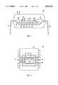
- FIG. 1illustrates one embodiment of a multi-chip module 20 in accordance with the present invention.
- the module 20, or simply, the circuit assembly 20,includes a first element 24 which is "stacked" on a semiconductor die 22.
- the semiconductor die 22has substantially parallel opposing first and second surfaces 30 and 28 with at least one electrical contact 32 being mounted on the first surface 30.
- the first element 24also has substantially parallel opposing first and second surfaces 36 and 34 with at least one electrical contact 38 being mounted on either the first or second surface 36 or 34. In the embodiment shown in FIG. 1, the electrical contact 38 is shown mounted on the first surface 36.
- the first element 24may be a semiconductor die or a substrate material. If the first element 24 is a substrate material, then it may be used as an interconnect media (discussed below).
- the substrate materialmay be, but is not limited to, ceramic, metal, silicon, or a plastic circuit board (PCB) material. Due its convenience and ready availability, a multilayer ceramic (MLC) substrate is quite popular.
- MLCmultilayer ceramic
- Metal substratesoffer other advantages of toughness (compared to MLC), high strength, inexpensive, and high thermal conductivity. With the proper combination of metal layers, such as Copper-Invar-Copper or Copper-Molybdenum-Copper, thermal mismatch between thin polymer films and the substrate can be minimized.
- Some typical base metalsinclude aluminum, copper, copper/molybdenum, copper/tungsten, Invar, and Kovar. Copper is one of the dominant base metals due to its high thermal conductivity, which tends to minimize thermal stresses.
- Silicon substrateshave the advantages of ready applicability of integrated circuit (IC) manufacturing techniques, possible incorporation of both active and passive devices, good thermal match with other silicon ICs attached to the substrate, and the dielectric layers can be either polyimide or SiO 2 , both of which are standard dielectrics in IC fabrication.
- the main disadvantages of silicon substratesare that they are expensive, the size is limited to wafer sizes, and silicon has a lower thermal conductivity than metal substrates.
- the semiconductor die 22may be mounted on a carrier member 42 and at least partially supported by a principal mounting surface (or seating plane) 40 of the carrier member 42.
- the phrase "mounted on a carrier member 42"is intended to mean that a particular element (in this case the die 22) is either directly attached to the carrier member 42, or that the particular element is attached to some other structure or combination of structures, such as another element, stack of elements, or adhesive materials, which are themselves directly attached to the carrier member 42.
- the carrier member 42generally includes two or more electrical leads 44 and 46.
- the carrier member 42is a lead frame, and the principal mounting surface 40 is a Die Attach Pad (DAP) of the lead frame 42.
- the electrical leads 44 and 46are the leads of the lead frame 42.
- the lead frame 42is housed within a mold compound 25 of a conventional molded plastic Dual Inline Package (DIP) 26.
- DIPDual Inline Package
- One advantage of the present inventionis that any of the three conventional semiconductor packages discussed above, i.e., molded plastic packages, cavity packages, and Chip-On-Board (COB) packages, may be used to house the stacked element and die 24 and 22. Furthermore, any other package having a principal mounting surface and electrical leads may also be used to house the stack.
- COBChip-On-Board
- the use of conventional packagesreduces cost and permits the multi-chip modules to be used immediately in existing electrical systems with little or no modification of the system.
- a DIPis shown in FIG. 1, it should be well understood that the stacked Multi-Chip Modules of the present invention may be housed in virtually any semiconductor package.
- the semiconductor die 22may be mounted to the principal mounting surface 40 by way of an adhesive material 48.
- the adhesive material 48may be an epoxy adhesive, soft solder, or any other adhesive suitable for mounting a die to a substrate.
- the adhesive material 48may be either electrically conductive or non-conductive. Conductivity is dictated by the type of fillers incorporated into the glue. For instance, metal fillers provide good electrical and thermal dissipation, while inorganic fillers such as fused silica or diamond enhance mainly the thermal performance.
- An example of an adhesive that works particularly well for ceramic packagesis part number 11 Staystik, manufactured by Staystik of Santa Aria, Calif.
- An example of an adhesive having aluminum nitride for high thermal conductivity for plastic packagesis part number 282 Staystik.
- the first element 24is also mounted to the carrier member 42.
- the first element 24is mounted such that it is at least partially supported at its second surface 34 by the first surface 30 of the die 22. Furthermore, the first element 24 is positioned such that the electrical contact 32 of the die 22 is exposed and is accessible for making electrical connections thereto. While the first element 24 shown in FIG. 1 is fully supported by the die 22, there are other embodiments of the present invention (discussed below) wherein a second element, along with the die 22, partially supports the first element 24.
- the first element 24may be mounted to the carrier member 42 by way of an adhesive material 50 applied to the first surface 30 of the die 22 and the second surface 34 of the first element 24.
- the adhesive 50may also be a conductive or nonconductive adhesive.
- the Staystik adhesives mentioned abovealso work particularly well here.
- Wire bondingis used to make electrical interconnections between the electrical contacts 32 and 58 of the die 22, the electrical contacts 38 and 54 of the first element 24, and the electrical leads 44 and 46. Because wire bonding is used to make the electrical interconnections among the die and other elements in the stack, the die and other elements should be stacked and positioned in such a manner that at least one of the electrical contacts of either the die and/or other elements is exposed and accessible for making fine wire connections thereto. As shown in FIG. 1, the first element 24 is smaller than the die 22, and thus, when the first element 24 is stacked in the center of the die 22, the electrical contacts 32 and 58 of the die 22 are exposed.
- the first element 24does not have to be smaller than the die 22; the first element 24 may be the same size, or even larger than the die 22, provided that the first element 24 is positioned on the die 22 in such a manner that at least one of the electrical contacts 32 or 58 is exposed and accessible for making fine wire connections thereto. As will be discussed below, there may even be a hole or slot through the first element 24 which exposes at least one of the electrical contacts of the die 22.
- the electrical contact 38 of the first element 24may be coupled to the electrical lead 46 by a fine wire conductor 52 which directly connects the contact 38 to the lead 46.
- An electrical contactmay also be indirectly coupled to a lead using wire bonding.
- the electrical contact 54may be coupled to the lead 44 by a fine wire conductor 56 connecting the contact 54 to a contact 58, and then another fine wire conductor 60 connecting the contact 58 to the lead 44.
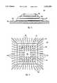
- FIG. 2illustrates the use of the first element 24 as an interconnect media, i.e., a surface where various long distance interconnections and line routing may be made.
- an elementis used as an interconnect media it is formed from one of the substrate materials discussed above.
- An example of a long distance interconnectionis the use of an electrical "strip" contact 68 to couple electrical contact 62 to lead 64.
- a fine wire conductor 66is used to connect contact 62 to one end of strip contact 68.
- Another fine wire conductor 70is used to connect the other end of strip contact 68 to lead 64.
- the first element 24when used as an interconnect media it may contain long strip contacts, similar to a printed circuit board, for transferring electrical signals from one side of the circuit assembly 20 to the other.
- FIG. 2illustrates the use of the first element 24 as an interconnect media, it should be understood that the first element 24 can alternatively be a semiconductor die, in which case similar interconnections from one die to the other may be made.
- the stacked configurationillustrates that expansion and layout in the third dimension (as opposed to the side-by-side layout) can increase the density of the MCM significantly.
- a larger number of dicecan be housed in a stacked MCM which increeses performance, power and versatility of the MCM.
- the dice or substratesmay be progressively smaller in size in the stacking order so that the bond pads can be exposed and accessed; however, progressively smaller sizing is not required as mentioned above.
- Dicemay be placed on top of each other, each attached to the other by either a non-conductive die attach or a thermoplastic tape fitting the footprint of the top die.
- the number of dice which can be contained in one stackmight be limited by the cavity height within a ceramic package or by the thickness of a molded plastic package.
- Substratescan be stacked with the dice to provide an interconnect media and a line routing means between the dice which helps to eliminate long wire bond lengths.
- a substrate placed on top of another diedoes not have to cover the whole die surface. It can also be used as an intermediate means of routing wiring to another die placed side by side the substrate.
- wire bondingcan be achieved with no wire cross over and acceptable levels of wire-to-wire separation.
- stacking dicecan provide configurations having wire bond lengths meeting standard assembly specifications. Maintaining short wire bond lengths minimizes the potential for wire sweep in the molding of the MCM.
- FIGS. 1 and 2illustrates a stacked MCM having only two elements, i.e., a die 22 and a die or substrate 24.
- a die 22i.e., a die 22 and a die or substrate 24.
- the present inventionencompasses the stacking of any number of elements where at least one of the elements in the stack is a semiconductor die having at least one other element on top of the die, and where the elements are stacked in such a manner that at least one electrical contact of at least one element is exposed and accessible for making wire bonding connections thereto.
- C4Controlled Collapse Chip Connection
- flip chipflip chip
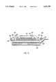
- FIG. 3illustrates another embodiment of the present invention having three stacked elements.
- the multi-chip module 72includes three elements 74, 76, and 78 mounted to the principal mounting surface 80 of a carrier member 82.
- Each of the elements 74, 76, and 78has planar opposing surfaces and may be either a semiconductor die or a substrate material, provided that at least one of elements 74 or 76 is a semiconductor die.
- the first element 74is mounted to the principal mounting surface 80 by way of an adhesive material 84
- the second element 76is mounted to the first element 74 by way of an adhesive material 86
- the third element 78is mounted to the second element 76 by way of an adhesive material 88.
- the third element 78should be at least partially supported by the second element 76, and the second element 76 should be at least partially supported by the first element 74. Furthermore, the second element 76 should be positioned such that the electrical contacts 94 and 100 of the first element 74 are exposed and accessible for making fine wire connections thereto. Likewise, the third element 78 may be positioned such that the electrical contacts 96 and 102 of the second element 76 are exposed and accessible for making fine wire connections thereto. Although the elements 76 and 78 are progressively smaller in size, this is not required, provided the elements are positioned such that at least one of the electrical contacts of the lower element is exposed.
- Wire bondingmay be used to electrically couple any or all of the contacts 94, 96, 98, 100, 102, and 104 to either or both of the electrical leads 106 and 108.
- fine wire conductors 110, 112, and 114couple the contacts 94, 96, and 98 to lead 108
- fine wire conductors 116, 118, and 120couple the contacts 100, 102, and 104 to lead 106.
- the carrier member 82may be any of the three conventional semiconductor packages discussed above.
- the multi-chip module 122 shown in FIG. 4includes three elements 124, 126, and 128 mounted on a carrier member 130 which has electrical leads 132 on only one side of the principal mounting surface 134.
- the multi-chip module 144 shown in FIG. 5includes three elements 146, 148, and 150 mounted on a carrier member 152.
- the carrier member 152is either a ceramic package or a metal can having electrical leads (not shown) mounted directly below the principal mounting surface 154.
- FIG. 6is a top view of a multi-chip module 156 having three elements 158, 160, and 162 mounted on the principal mounting surface 164 of a carrier member 166.
- the carrier member 166includes electrical leads 168 on all four sides of the carrier member 166.
- FIG. 7illustrates a multi-chip module 135 having three elements 136, 138, and 140 mounted on a carrier member 142.
- the first and third elements 136 and 140are semiconductor dice, and the second element 138 is a substrate material.
- FIG. 8illustrates another embodiment of a multi-chip module 170 in accordance with the present invention.
- Four elements 172, 174, 176, and 180are mounted on the principal mounting surface 182 of a carrier member 184.
- Each of the elements 172, 174, 176, and 180has planar opposing surfaces and may be either a semiconductor die or a substrate material, provided that at least one of the elements 172, 174, or 176 is a die.
- the second and third elements 174 and 176are both supported by the first element 172.
- the fourth element 178is partially supported by the second element 174 and partially supported by the third element 176.
- elements 174 and 176are positioned such that at least one of the electrical contacts of element 172 is exposed for wire bonding
- element 178is positioned such that at least one of the electrical contacts of either element 174 or 176 is exposed for wire bonding.
- Adhesive materials 186, 188, and 190are used to mount each of the elements 172, 174, 176, and 180 to the carrier 184.
- the carrier member 184may be the carrier of any type of conventional semiconductor package.
- FIG. 9illustrates basically the same embodiment shown in FIG. 8, except that the carrier member 192 is the type found in a ceramic package or a metal can.
- FIG. 10illustrates another embodiment of a multi-chip module 193 in accordance with the present invention.
- Four elements 194, 196, 198, and 200are mounted on the principal mounting surface 202 of a carrier member 204. Each of the elements 194, 196, 198, and 200 has planar opposing surfaces.
- the elements 194 and 198are semiconductor dice, and the elements 196 and 200 may each be either a semiconductor die or a substrate material.
- the four elements 194, 196, 198, and 200are arranged in two separate stacks 206 and 208.
- the first stack 206includes the first element 194 mounted on the principal mounting surface 202 and the second element 196 being at least partially supported by the first element 194.
- the second stack 208includes the third element 198 mounted on the principal mounting surface 202 and the fourth element 200 being at least partially supported by the third element 198.
- FIG. 11illustrates another embodiment of a multi-chip module 210 in accordance with the present invention.
- Three elements 212, 214, and 216are mounted on the principal mounting surface 218 of a carrier member 220.
- Each of the elements 212, 214, and 216has planar opposing surfaces and may be either a semiconductor die or a substrate material, provided that at least one of elements 214 or 216 is a die.
- the first element 212is mounted on the principal mounting surface 218, the second element 214 is at least partially supported by the first element 212, and the third element 216 is at least partially supported by the second element 214.
- the principal difference between the multi-chip module 210 and the other embodiments discussed aboveis that the second element 214 has holes (or slots) 222 and 224 extending through the second element 214 from the first surface 226 to the second surface 228.
- holes 222 and 224The purpose of the holes 222 and 224 is to expose and make accessible the electrical contacts 236 and 242 of the element 212 for making fine wire connections thereto.
- element 214is positioned in such a manner that the electrical contacts 236 and 242 are exposed and accessible through the holes 222 and 224.
- wire bonding interconnectionscan be made between the elements 216, 214, and 212 even if element 214 is larger than element 212.
- fine wire conductor 230extends from electrical contact 234 through the hole 224 and makes contact with electrical contact 236.
- fine wire conductor 238extends from electrical contact 240 through the hole 222 and makes contact with electrical contact 242.
- the holes 222 and 224permit a direct electrical connection to be made via a fine wire conductor between the first element 212 and the third element 216.
- the second element 214would be larger than the first element 212 is to permit the first surface 226 to accommodate a large amount of circuitry for making many interconnections between the first and second elements 212 and 216.
- the second element 214will be a substrate material for use as an interconnect media.
- the second element 214could also be a semiconductor die having holes on portions of the die where there is no circuitry.
- FIG. 12illustrates one manner in which a hole or slot 244 may be formed through an element having parallel opposing surfaces.
- the hole 244may be any desired size or shape; for example, the hole 244 may be a small round hole, a long rectangular hole, a square hole, etc.
- FIG. 13illustrates a second element 250 which is sandwiched between a first element 248 and a third element 252.
- the second element 250has a cut-away portion 254 which permits the fine wire conductors 256 to extend from the third element 252 to the first element 248.
- a cut-away portion in any one of the elementsmay serve a similar purpose of a hole or slot.
- FIG. 14illustrates a multi-chip module 258 having three elements 260, 262, and 264 mounted on the principal mounting surface 266 of a carrier member 268.
- the second element 262includes holes 270 and 272.
- the carrier member 268is of the type found in a ceramic package or metal can.
- FIG. 15is a top view of a multi-chip module 274 having three elements 276, 278, and 280 mounted on the principal mounting surface 282 of a carrier member 284.
- the carrier member 284is of a type having electrical leads 286 on all four sides of the principal mounting surface 282.
- the second element 278includes four slots 288, 290, 292, and 294 extending therethrough to expose the electrical contacts of the first element 276.
- fine wire conductor 296is permitted to extend from the third element 280 through the slot 292 to the first element 276.
- a method of manufacturing the multi-chip module 20begins with applying an adhesive or soft-solder 48 on the principal mounting surface 40 of the carrier member 42.
- a semiconductor die 22is then dispensed onto the adhesive 48 with a pressure of about 8-10 pounds per square-inch (psi).
- the next stepis to apply an adhesive or epoxy 50 onto the first surface 30 of the die 22.
- a first element 24is then dispensed onto the adhesive 50 with a pressure of about 3-5 psi.
- the first element 24should be at least partially supported by the die 22, and furthermore, the first element 24 should be positioned such that at least one of the electrical contacts of the die 22 is exposed and accessible for making wire bonding connections thereto.
- the first element 24may be a semiconductor die or a substrate material.
- an adhesive or epoxyis applied to the first surface 36 of the first element 24 and a second element is dispensed onto the first surface 36. If additional elements are desired, the same steps of applying an adhesive or epoxy onto the surface of the last dispensed element and then dispensing another element onto the last element are followed.
- the electrical contacts on the elementssuch as contacts 32, 38, 54, and 58, and the electrical leads on the carrier 42, such as leads 44 and 46, are wire bonded together.
- the carrier member 42is sealed in the semiconductor package 26.
- This stepusually entails forming the mold compound 25 around the carrier 42 such that the die and first element 22 and 24 are completely covered with mold compound 25 and only the leads 44 and 46 are exposed.
- the semiconductor package 26is a DIP, it should be understood that any conventional semiconductor package may be used.
- An alternative method of manufacturing the multi-chip module 20begins with pre-assembling the stacked die and first element 22 and 24, and then mounting the pre-assembled stack onto the carrier member 42.
- the desired number of elementswhether it be two, three, four, etc., are first stacked and bonded together with adhesive.
- the stackis then mounted on the principal mounting surface 40. After wire bonding interconnections are made, the circuit assembly is sealed in the semiconductor package.
- This alternative methodhas the advantage that all of the dice are mounted on the carrier member in a single step rather than each separate die being mounted on the carrier member one at a time.
Landscapes
- Engineering & Computer Science (AREA)
- Computer Hardware Design (AREA)
- Microelectronics & Electronic Packaging (AREA)
- Power Engineering (AREA)
- Physics & Mathematics (AREA)
- Condensed Matter Physics & Semiconductors (AREA)
- General Physics & Mathematics (AREA)
- Wire Bonding (AREA)
- Lead Frames For Integrated Circuits (AREA)
- Structures For Mounting Electric Components On Printed Circuit Boards (AREA)
Abstract
Description
This is a continuation of application Ser. No. 07/887,774, filed May 22, 1992, now U.S. Pat. No. 5,422,435.
1. Field of the Invention
The present invention relates to semiconductor packaging technologies, and more particularly, to semiconductor packages which contain multiple semiconductor dice and/or substrates.
2. Description of the Related Art
Very Large Scale Integrated (VLSI) semiconductor dice are usually housed in semiconductor packages. Normally, one semiconductor package contains only one die.
There are three conventional types of semiconductor packages. Molded plastic packages contain a lead frame molded within a plastic body. A lead frame is a sheet metal framework having several electrical leads and a Die Attach Pad (DAP) serving as a principal mounting surface (or seating plane) upon which a die is mounted. The die may be bonded either directly to the DAP or to a substrate attached to the DAP. The electrical leads provide an electrical path from inside the molded plastic to outside the plastic. Some common types of molded plastic packages are: Plastic Chip Carrier (PCC), Molded Dual Inline Package (MDIP), Plastic Quad Flat Pack (PQFP), Small Outline (SO), Shrink Small Outline Package (SSOP), Transistor Outline Package (TO), Very Small Outline Package (VSOP), and Thin Small Outline Package (TSOP).
The second conventional type of semiconductor package is the cavity package. In the cavity package, a cavity base which serves as a principal mounting surface (or seating plane) upon which a die is mounted is contained within a hollow housing. Unlike the molded plastic package, the die in a cavity package is surrounded by air. Several electrical leads provide an electrical path from inside the housing to outside the housing. Some common types of cavity packages are ceramic packages, metal cans, plastic packages, and any combination thereof.
The third conventional type of semiconductor configuration is the Chip-On-Board (COB) assembly. In the COB, a die is directly bonded to a circuit board or substrate which serves as a principal mounting surface (or seating plane). The die is usually covered and protected with a plastic material. A variety of different types of electrical leads may be employed to provide an electrical path from inside the plastic material to outside the plastic material.
Although the three conventional types of semiconductor packages have various different shapes and sizes, each of them includes several electrical leads and a principal mounting surface (or seating plane) upon which a die is mounted.
A common method of making electrical connections between the die and the electrical leads, which is used in each of the three conventional types of packages, is wire bonding. Wire bonding is a method of making electrical interconnections among components in a discrete package by means of fine wire conductors welded to the individual components. Thus, a fine wire conductor has one end connected to an electrical lead and the other end connected to an electrical contact on the die. Wire bonding is a popular method of interconnecting dice. Improvements in capillary design, wire bonding process control, and wire properties have allowed finer pitch bonding to be made.
Often two or more semiconductor dice are electrically interconnected to provide a single circuit assembly. Under the one die per package paradigm, the interconnection of two or more dice requires enough physical space for an equal number of packages. In order to decrease size and weight, as well as improve device performance, there have been several attempts to combine two or more dice into a single package. In the high density integrated circuit packaging industry, the combination of two or more dice in a single package is typically referred to as a Multi-Chip Module (MCM) or Multi-Chip Package (MCP). Although the terms Multi-Chip Module and Multi-Chip Package have slightly different meanings, for purposes of this discussion, they may be used interchangeably.
The most common MCM is the "side-by-side" MCM. In this version two or more dice are mounted next to each other (or side by side each other) on the principal mounting surface of either a plastic molded package, cavity package, or COB package. The die may be mounted directly to the principal mounting surface or it may be mounted on a substrate material which is itself mounted directly to the principal mounting surface. Interconnections among the dice and electrical leads are commonly made via wire bonding.
The side-by-side MCM, however, suffers from a number of disadvantages. Laying out the dice side by side on the principal mounting surface within a molded plastic package or a cavity package is not the most optimal way to use package real estate. Such real estate is preciously limited since, in most cases, the dice have to fit within some standard form factor previously designed for only one die. If the dice are not properly laid out, the real estate restriction will limit the number of dice that can be incorporated into the MCM. Furthermore, unoptimized dice layout yields correspondingly unoptimized wire bonding resulting in wire cross over, long wire lengths and small wire-to-wire separation. Wire cross over, where one wire loops over another wire, is highly undesirable because shorting may occur as a result of molding conditions. Similarly, long wire lengths and small wire-to-wire separation can pose high risks for wire sweep under fast mold transfer conditions or high resin viscosity.
Other attempts at building MCMs have involved placing two or more dice on top of one another and then securing the "stack" of dice in a package. Currently available stacked MCMs are fabricated by stacking entire wafers and then sawing the stacked wafers into stacked dice. Thus, each of the individual die in a particular stack is the same size.
One disadvantage of currently available stacked MCMs is that they are all memory devices; it is believed that no mixed technology devices are currently available in stacked form. Another disadvantage of currently available stacked MCMs is that they require unique and specialized packages. Furthermore, complex and expensive methods are used to make electrical interconnections among the dice; the methods of interconnection currently used are Controlled Collapse Chip Connection (C4) and Tape Automated Bonding (TAB).
Controlled Collapse Chip Connection (C4), also known as "flip chip", involves the use of a large number of solder bumps on a die surface which allow it to be bonded face down. Among the advantages are improved thermal performance, electrical characteristics and reworkability. On the other hand, commonly acknowledged disadvantages include requirements for precise alignment, difficulties in cleaning and inspection, uniform solder joint height for all connections to be made and a substrate with low coefficient of thermal expansion for longer thermal cycle life. Furthermore, in order to use C4, all solder bumps and interconnections must be implemented before and during the stacking of the dice; in other words, after the dice are stacked, no additional interconnections can be made.
Tape Automated Bonding (TAB) refers to a process whereby dice are joined by patterned metal on polymeric tape using thermocompression bonding. Subsequent attachment to a substrate or board is carried out by outer lead bonding. Tape Automated Bonding (TAB) has seen only limited application to MCMs. Although TAB possesses many advantages, barriers to its wide usage include the high starting cost of custom tape, the moisture sensitivity of polyimide tape and the need to switch to single point bonding with large dies to circumvent planarity issues.
Thus, there is a need for a low cost MCM which overcomes the disadvantages of currently available MCMs.
The present invention provides a circuit assembly having a semiconductor die which has substantially parallel opposing first and second surfaces and at least one electrical contact mounted on the first surface. A first element having substantially parallel opposing first and second surfaces and at least one electrical contact mounted on one of its surfaces is mounted on and at least partially supported at its second surface by the first surface of the semiconductor die. The first element is positioned such that the semiconductor die electrical contact is exposed. A fine wire conductor having first and second ends is connected at its first end to either the semiconductor die electrical contact or the first element electrical contact.
A method of manufacturing the above circuit assembly includes the steps of dispensing the semiconductor die onto a carrier member having a principal mounting surface and a plurality of electrical leads. The semiconductor die should be at least partially supported at its second surface by the principal mounting surface. The first element is then dispensed onto the semiconductor die first surface. The first element should be at least partially supported at its second surface by the semiconductor die, and the first element should be positioned such that the semiconductor die electrical contact is exposed.
A better understanding of the features and advantages of the present invention will be obtained by reference to the following detailed description of the invention and accompanying drawings which set forth an illustrative embodiment in which the principles of the invention are utilized.
FIG. 1 is a cross-sectional view of a multi-chip module in accordance with the present invention.
FIG. 2 is a top view of the multi-chip module of FIG. 1.
FIG. 3 is a cross-sectional view of an embodiment of a multi-chip module in accordance with the present invention having three elements.
FIG. 4 is a cross-sectional view of an alternative embodiment of a multi-chip module in accordance with the present invention having three elements.
FIG. 5 is a cross-sectional view of a second alternative embodiment of a multi-chip module in accordance with the present invention having three elements.
FIG. 6 is a top view of a third alternative embodiment of a multi-chip module in accordance with the present invention having three elements.
FIG. 7 is a cross-sectional view of a fourth alternative embodiment of a multi-chip module in accordance with the present invention having three elements.
FIG. 8 is a cross-sectional view of an embodiment of a multi-chip module in accordance with the present invention having four elements.
FIG. 9 is a cross-sectional view of a first alternative embodiment of a multi-chip module in accordance with the present invention having four elements.
FIG. 10 is a cross-sectional view of a second alternative embodiment of a multi-chip module in accordance with the present invention having four elements.
FIG. 11 is a cross-sectional view of an embodiment of a multi-chip module in accordance with the present invention having three elements with one of the elements having at least one hole or slot therethrough.
FIG. 12 is an isometric view of an element having a hole or slot therethrough.
FIG. 13 is an isometric view of three elements wherein one of the has a cut-away section.
FIG. 14 is a cross-sectional view of an alternative embodiment of a multi-chip module in accordance with the present invention having three elements with one of the elements having at least one hole or slot therethrough.
FIG. 15 is a top view of a second alternative embodiment of a multi-chip module in accordance with the present invention having three elements with one of the elements having at least one hole or slot therethrough.
FIG. 1 illustrates one embodiment of amulti-chip module 20 in accordance with the present invention. Themodule 20, or simply, thecircuit assembly 20, includes afirst element 24 which is "stacked" on asemiconductor die 22. The semiconductor die 22 has substantially parallel opposing first andsecond surfaces electrical contact 32 being mounted on thefirst surface 30. Thefirst element 24 also has substantially parallel opposing first andsecond surfaces electrical contact 38 being mounted on either the first orsecond surface electrical contact 38 is shown mounted on thefirst surface 36.
Thefirst element 24 may be a semiconductor die or a substrate material. If thefirst element 24 is a substrate material, then it may be used as an interconnect media (discussed below). The substrate material may be, but is not limited to, ceramic, metal, silicon, or a plastic circuit board (PCB) material. Due its convenience and ready availability, a multilayer ceramic (MLC) substrate is quite popular. Metal substrates offer other advantages of toughness (compared to MLC), high strength, inexpensive, and high thermal conductivity. With the proper combination of metal layers, such as Copper-Invar-Copper or Copper-Molybdenum-Copper, thermal mismatch between thin polymer films and the substrate can be minimized. Some typical base metals include aluminum, copper, copper/molybdenum, copper/tungsten, Invar, and Kovar. Copper is one of the dominant base metals due to its high thermal conductivity, which tends to minimize thermal stresses. Silicon substrates have the advantages of ready applicability of integrated circuit (IC) manufacturing techniques, possible incorporation of both active and passive devices, good thermal match with other silicon ICs attached to the substrate, and the dielectric layers can be either polyimide or SiO2, both of which are standard dielectrics in IC fabrication. On the other hand, the main disadvantages of silicon substrates are that they are expensive, the size is limited to wafer sizes, and silicon has a lower thermal conductivity than metal substrates.
The semiconductor die 22 may be mounted on acarrier member 42 and at least partially supported by a principal mounting surface (or seating plane) 40 of thecarrier member 42. The phrase "mounted on acarrier member 42" is intended to mean that a particular element (in this case the die 22) is either directly attached to thecarrier member 42, or that the particular element is attached to some other structure or combination of structures, such as another element, stack of elements, or adhesive materials, which are themselves directly attached to thecarrier member 42.
Thecarrier member 42 generally includes two or moreelectrical leads carrier member 42 is a lead frame, and theprincipal mounting surface 40 is a Die Attach Pad (DAP) of thelead frame 42. The electrical leads 44 and 46 are the leads of thelead frame 42. Thelead frame 42 is housed within amold compound 25 of a conventional molded plastic Dual Inline Package (DIP) 26.
One advantage of the present invention is that any of the three conventional semiconductor packages discussed above, i.e., molded plastic packages, cavity packages, and Chip-On-Board (COB) packages, may be used to house the stacked element and die 24 and 22. Furthermore, any other package having a principal mounting surface and electrical leads may also be used to house the stack. The use of conventional packages reduces cost and permits the multi-chip modules to be used immediately in existing electrical systems with little or no modification of the system. Thus, while a DIP is shown in FIG. 1, it should be well understood that the stacked Multi-Chip Modules of the present invention may be housed in virtually any semiconductor package.
The semiconductor die 22 may be mounted to theprincipal mounting surface 40 by way of anadhesive material 48. Theadhesive material 48 may be an epoxy adhesive, soft solder, or any other adhesive suitable for mounting a die to a substrate. Theadhesive material 48 may be either electrically conductive or non-conductive. Conductivity is dictated by the type of fillers incorporated into the glue. For instance, metal fillers provide good electrical and thermal dissipation, while inorganic fillers such as fused silica or diamond enhance mainly the thermal performance. An example of an adhesive that works particularly well for ceramic packages is part number 11 Staystik, manufactured by Staystik of Santa Aria, Calif. An example of an adhesive having aluminum nitride for high thermal conductivity for plastic packages ispart number 282 Staystik.
Thefirst element 24 is also mounted to thecarrier member 42. Thefirst element 24 is mounted such that it is at least partially supported at itssecond surface 34 by thefirst surface 30 of thedie 22. Furthermore, thefirst element 24 is positioned such that theelectrical contact 32 of the die 22 is exposed and is accessible for making electrical connections thereto. While thefirst element 24 shown in FIG. 1 is fully supported by thedie 22, there are other embodiments of the present invention (discussed below) wherein a second element, along with the die 22, partially supports thefirst element 24.
Thefirst element 24 may be mounted to thecarrier member 42 by way of anadhesive material 50 applied to thefirst surface 30 of thedie 22 and thesecond surface 34 of thefirst element 24. The adhesive 50 may also be a conductive or nonconductive adhesive. The Staystik adhesives mentioned above also work particularly well here.
Wire bonding is used to make electrical interconnections between theelectrical contacts electrical contacts first element 24, and the electrical leads 44 and 46. Because wire bonding is used to make the electrical interconnections among the die and other elements in the stack, the die and other elements should be stacked and positioned in such a manner that at least one of the electrical contacts of either the die and/or other elements is exposed and accessible for making fine wire connections thereto. As shown in FIG. 1, thefirst element 24 is smaller than the die 22, and thus, when thefirst element 24 is stacked in the center of the die 22, theelectrical contacts first element 24 does not have to be smaller than the die 22; thefirst element 24 may be the same size, or even larger than the die 22, provided that thefirst element 24 is positioned on the die 22 in such a manner that at least one of theelectrical contacts first element 24 which exposes at least one of the electrical contacts of thedie 22.
The particular interconnections which are made using the wire bonding method may vary and depend upon the particular application for which themulti-chip module 20 is to be used. For example, theelectrical contact 38 of thefirst element 24 may be coupled to theelectrical lead 46 by afine wire conductor 52 which directly connects thecontact 38 to thelead 46. An electrical contact may also be indirectly coupled to a lead using wire bonding. For example, theelectrical contact 54 may be coupled to thelead 44 by afine wire conductor 56 connecting thecontact 54 to acontact 58, and then anotherfine wire conductor 60 connecting thecontact 58 to thelead 44.
FIG. 2 illustrates the use of thefirst element 24 as an interconnect media, i.e., a surface where various long distance interconnections and line routing may be made. When an element is used as an interconnect media it is formed from one of the substrate materials discussed above. An example of a long distance interconnection is the use of an electrical "strip"contact 68 to coupleelectrical contact 62 to lead 64. Specifically, a fine wire conductor 66 is used to connectcontact 62 to one end ofstrip contact 68. Another fine wire conductor 70 is used to connect the other end ofstrip contact 68 to lead 64. Thus, when thefirst element 24 is used as an interconnect media it may contain long strip contacts, similar to a printed circuit board, for transferring electrical signals from one side of thecircuit assembly 20 to the other. Again, the particular interconnections which are made will vary and depend upon the particular application for which themulti-chip module 20 is to be used. Furthermore, while FIG. 2 illustrates the use of thefirst element 24 as an interconnect media, it should be understood that thefirst element 24 can alternatively be a semiconductor die, in which case similar interconnections from one die to the other may be made.
The stacked configuration illustrates that expansion and layout in the third dimension (as opposed to the side-by-side layout) can increase the density of the MCM significantly. For the same amount of space, a larger number of dice can be housed in a stacked MCM which increeses performance, power and versatility of the MCM. The dice or substrates may be progressively smaller in size in the stacking order so that the bond pads can be exposed and accessed; however, progressively smaller sizing is not required as mentioned above.
Different variations of the stacking structure can be implemented in order to optimize the utilization of the third dimension. Dice may be placed on top of each other, each attached to the other by either a non-conductive die attach or a thermoplastic tape fitting the footprint of the top die. The number of dice which can be contained in one stack might be limited by the cavity height within a ceramic package or by the thickness of a molded plastic package.
Substrates can be stacked with the dice to provide an interconnect media and a line routing means between the dice which helps to eliminate long wire bond lengths. A substrate placed on top of another die does not have to cover the whole die surface. It can also be used as an intermediate means of routing wiring to another die placed side by side the substrate.
By using the proper layout of dice or dice/substrate combinations, wire bonding can be achieved with no wire cross over and acceptable levels of wire-to-wire separation. Furthermore, stacking dice can provide configurations having wire bond lengths meeting standard assembly specifications. Maintaining short wire bond lengths minimizes the potential for wire sweep in the molding of the MCM.
The embodiment of the present invention shown in FIGS. 1 and 2 illustrates a stacked MCM having only two elements, i.e., adie 22 and a die orsubstrate 24. However, there is no limitation on the number of elements which can be stacked. The present invention encompasses the stacking of any number of elements where at least one of the elements in the stack is a semiconductor die having at least one other element on top of the die, and where the elements are stacked in such a manner that at least one electrical contact of at least one element is exposed and accessible for making wire bonding connections thereto. Note that some of the elements in the stack may be interconnected by using Controlled Collapse Chip Connection (C4), or "flip chip" connection, provided that the elements are stacked in such a manner that at least one electrical contact of at least one element is exposed and accessible for making wire bonding connections thereto.
FIG. 3 illustrates another embodiment of the present invention having three stacked elements. Themulti-chip module 72 includes threeelements principal mounting surface 80 of acarrier member 82. Each of theelements elements first element 74 is mounted to theprincipal mounting surface 80 by way of anadhesive material 84, thesecond element 76 is mounted to thefirst element 74 by way of anadhesive material 86, and thethird element 78 is mounted to thesecond element 76 by way of anadhesive material 88. Thethird element 78 should be at least partially supported by thesecond element 76, and thesecond element 76 should be at least partially supported by thefirst element 74. Furthermore, thesecond element 76 should be positioned such that theelectrical contacts 94 and 100 of thefirst element 74 are exposed and accessible for making fine wire connections thereto. Likewise, thethird element 78 may be positioned such that theelectrical contacts second element 76 are exposed and accessible for making fine wire connections thereto. Although theelements
Wire bonding may be used to electrically couple any or all of thecontacts electrical leads fine wire conductors contacts fine wire conductors contacts
Thecarrier member 82 may be any of the three conventional semiconductor packages discussed above. For example, themulti-chip module 122 shown in FIG. 4 includes threeelements carrier member 130 which haselectrical leads 132 on only one side of the principal mountingsurface 134. Themulti-chip module 144 shown in FIG. 5 includes threeelements carrier member 152. Thecarrier member 152 is either a ceramic package or a metal can having electrical leads (not shown) mounted directly below theprincipal mounting surface 154. FIG. 6 is a top view of amulti-chip module 156 having threeelements principal mounting surface 164 of acarrier member 166. Thecarrier member 166 includeselectrical leads 168 on all four sides of thecarrier member 166.
Any combination of the three elements may be either semiconductor dice and/or a substrate material, provided that the uppermost element is not the only die. Again, the choice of die or substrate, as well as the particular wire bonding interconnections to be made, depends upon the particular application for which the multi-chip module is to be used. FIG. 7 illustrates amulti-chip module 135 having threeelements carrier member 142. The first andthird elements second element 138 is a substrate material.
FIG. 8 illustrates another embodiment of amulti-chip module 170 in accordance with the present invention. Fourelements principal mounting surface 182 of acarrier member 184. Each of theelements elements third elements first element 172. Thefourth element 178 is partially supported by thesecond element 174 and partially supported by thethird element 176. Furthermore,elements element 172 is exposed for wire bonding, andelement 178 is positioned such that at least one of the electrical contacts of eitherelement Adhesive materials elements carrier 184. Again, thecarrier member 184 may be the carrier of any type of conventional semiconductor package. FIG. 9 illustrates basically the same embodiment shown in FIG. 8, except that thecarrier member 192 is the type found in a ceramic package or a metal can.
FIG. 10 illustrates another embodiment of amulti-chip module 193 in accordance with the present invention. Fourelements principal mounting surface 202 of acarrier member 204. Each of theelements elements elements elements separate stacks first stack 206 includes thefirst element 194 mounted on theprincipal mounting surface 202 and thesecond element 196 being at least partially supported by thefirst element 194. Thesecond stack 208 includes thethird element 198 mounted on theprincipal mounting surface 202 and thefourth element 200 being at least partially supported by thethird element 198.
FIG. 11 illustrates another embodiment of amulti-chip module 210 in accordance with the present invention. Threeelements principal mounting surface 218 of acarrier member 220. Each of theelements elements first element 212 is mounted on theprincipal mounting surface 218, thesecond element 214 is at least partially supported by thefirst element 212, and thethird element 216 is at least partially supported by thesecond element 214. The principal difference between themulti-chip module 210 and the other embodiments discussed above is that thesecond element 214 has holes (or slots) 222 and 224 extending through thesecond element 214 from thefirst surface 226 to thesecond surface 228.
The purpose of theholes electrical contacts 236 and 242 of theelement 212 for making fine wire connections thereto. In other words,element 214 is positioned in such a manner that theelectrical contacts 236 and 242 are exposed and accessible through theholes holes electrical contacts 236 and 242, wire bonding interconnections can be made between theelements element 214 is larger thanelement 212. For example,fine wire conductor 230 extends fromelectrical contact 234 through thehole 224 and makes contact withelectrical contact 236. As another example,fine wire conductor 238 extends fromelectrical contact 240 through thehole 222 and makes contact with electrical contact 242. Thus, if thesecond element 214 is larger than thefirst element 212 such that it is completely covered by thesecond element 214, theholes first element 212 and thethird element 216.
One reason that thesecond element 214 would be larger than thefirst element 212 is to permit thefirst surface 226 to accommodate a large amount of circuitry for making many interconnections between the first andsecond elements second element 214 will be a substrate material for use as an interconnect media. However, thesecond element 214 could also be a semiconductor die having holes on portions of the die where there is no circuitry.
FIG. 12 illustrates one manner in which a hole or slot 244 may be formed through an element having parallel opposing surfaces. Thehole 244 may be any desired size or shape; for example, thehole 244 may be a small round hole, a long rectangular hole, a square hole, etc.
FIG. 13 illustrates asecond element 250 which is sandwiched between afirst element 248 and athird element 252. Instead of using a hole or slot, thesecond element 250 has a cut-awayportion 254 which permits thefine wire conductors 256 to extend from thethird element 252 to thefirst element 248. Thus, a cut-away portion in any one of the elements may serve a similar purpose of a hole or slot.
FIG. 14 illustrates amulti-chip module 258 having threeelements principal mounting surface 266 of acarrier member 268. Thesecond element 262 includesholes carrier member 268 is of the type found in a ceramic package or metal can. FIG. 15 is a top view of amulti-chip module 274 having threeelements principal mounting surface 282 of acarrier member 284. Thecarrier member 284 is of a type havingelectrical leads 286 on all four sides of the principal mountingsurface 282. Thesecond element 278 includes fourslots first element 276. Thus,fine wire conductor 296 is permitted to extend from thethird element 280 through theslot 292 to thefirst element 276.
Referring back to FIG. 1, a method of manufacturing themulti-chip module 20 begins with applying an adhesive or soft-solder 48 on theprincipal mounting surface 40 of thecarrier member 42. A semiconductor die 22 is then dispensed onto the adhesive 48 with a pressure of about 8-10 pounds per square-inch (psi).
The next step is to apply an adhesive or epoxy 50 onto thefirst surface 30 of thedie 22. Afirst element 24 is then dispensed onto the adhesive 50 with a pressure of about 3-5 psi. Thefirst element 24 should be at least partially supported by thedie 22, and furthermore, thefirst element 24 should be positioned such that at least one of the electrical contacts of the die 22 is exposed and accessible for making wire bonding connections thereto. Thefirst element 24 may be a semiconductor die or a substrate material.
If a second element is desired, an adhesive or epoxy is applied to thefirst surface 36 of thefirst element 24 and a second element is dispensed onto thefirst surface 36. If additional elements are desired, the same steps of applying an adhesive or epoxy onto the surface of the last dispensed element and then dispensing another element onto the last element are followed.
After the desired number of elements are mounted on thecarrier 42, then the electrical contacts on the elements, such ascontacts carrier 42, such as leads 44 and 46, are wire bonded together.
After the wire bonding is complete, thecarrier member 42 is sealed in thesemiconductor package 26. This step usually entails forming themold compound 25 around thecarrier 42 such that the die andfirst element mold compound 25 and only theleads semiconductor package 26 is a DIP, it should be understood that any conventional semiconductor package may be used.
An alternative method of manufacturing themulti-chip module 20 begins with pre-assembling the stacked die andfirst element carrier member 42. In other words, the desired number of elements, whether it be two, three, four, etc., are first stacked and bonded together with adhesive. The stack is then mounted on theprincipal mounting surface 40. After wire bonding interconnections are made, the circuit assembly is sealed in the semiconductor package. This alternative method has the advantage that all of the dice are mounted on the carrier member in a single step rather than each separate die being mounted on the carrier member one at a time.
It should be understood that various alternatives to the embodiments of the invention described herein may be employed in practicing the invention. It is intended that the following claims define the scope of the invention and that structures and methods within the scope of these claims and their equivalents be covered thereby.
Claims (4)
1. A circuit assembly, comprising:
a first semiconductor die having substantially parallel opposing first and second surfaces and at least one electrical contact disposed at the first semiconductor die first surface;
a second semiconductor die having substantially parallel opposing first and second surfaces and at least one electrical contact disposed at the second semiconductor die first surface, the second semiconductor die being positioned so that its first surface is substantially coplanar with the first semiconductor die first surface;
a third semiconductor die having substantially parallel opposing first and second surfaces and at least one electrical contact disposed at the third semiconductor die first surface, the third semiconductor die being mounted on and supported at its second surface by the first and second semiconductor die first surfaces, the third semiconductor die being positioned so that the first and second semiconductor die electrical contacts are exposed; and
a fine wire conductor having first-and second ends, the first end being connected to the third semiconductor die electrical contact.
2. The circuit assembly of claim 1, wherein the second end of the fine wire conductor is connected to one of the first and second semiconductor die electrical contacts.
3. The circuit assembly of claim 1, further comprising:
a carrier member having a principal mounting surface and a plurality of electrical leads, wherein the first and second semiconductor dies are at least partially supported at their second surfaces by the principal mounting surface.
4. The circuit assembly of claim 3, wherein the second end of the fine wire conductor is connected to one of the plurality of electrical leads.
Priority Applications (1)
| Application Number | Priority Date | Filing Date | Title |
|---|---|---|---|
| US08/462,812US5495398A (en) | 1992-05-22 | 1995-06-05 | Stacked multi-chip modules and method of manufacturing |
Applications Claiming Priority (2)
| Application Number | Priority Date | Filing Date | Title |
|---|---|---|---|
| US07/887,774US5422435A (en) | 1992-05-22 | 1992-05-22 | Stacked multi-chip modules and method of manufacturing |
| US08/462,812US5495398A (en) | 1992-05-22 | 1995-06-05 | Stacked multi-chip modules and method of manufacturing |
Related Parent Applications (1)
| Application Number | Title | Priority Date | Filing Date |
|---|---|---|---|
| US07/887,774ContinuationUS5422435A (en) | 1992-05-22 | 1992-05-22 | Stacked multi-chip modules and method of manufacturing |
Publications (1)
| Publication Number | Publication Date |
|---|---|
| US5495398Atrue US5495398A (en) | 1996-02-27 |
Family
ID=25391830
Family Applications (3)
| Application Number | Title | Priority Date | Filing Date |
|---|---|---|---|
| US07/887,774Expired - LifetimeUS5422435A (en) | 1992-05-22 | 1992-05-22 | Stacked multi-chip modules and method of manufacturing |
| US08/403,061Expired - LifetimeUS5502289A (en) | 1992-05-22 | 1995-03-13 | Stacked multi-chip modules and method of manufacturing |
| US08/462,812Expired - LifetimeUS5495398A (en) | 1992-05-22 | 1995-06-05 | Stacked multi-chip modules and method of manufacturing |
Family Applications Before (2)
| Application Number | Title | Priority Date | Filing Date |
|---|---|---|---|
| US07/887,774Expired - LifetimeUS5422435A (en) | 1992-05-22 | 1992-05-22 | Stacked multi-chip modules and method of manufacturing |
| US08/403,061Expired - LifetimeUS5502289A (en) | 1992-05-22 | 1995-03-13 | Stacked multi-chip modules and method of manufacturing |
Country Status (5)
| Country | Link |
|---|---|
| US (3) | US5422435A (en) |
| EP (1) | EP0575051B1 (en) |
| JP (1) | JP3356821B2 (en) |
| KR (1) | KR100282285B1 (en) |
| DE (1) | DE69325749T2 (en) |
Cited By (133)
| Publication number | Priority date | Publication date | Assignee | Title |
|---|---|---|---|---|
| US5696031A (en)* | 1996-11-20 | 1997-12-09 | Micron Technology, Inc. | Device and method for stacking wire-bonded integrated circuit dice on flip-chip bonded integrated circuit dice |
| US5723907A (en)* | 1996-06-25 | 1998-03-03 | Micron Technology, Inc. | Loc simm |
| US5790384A (en)* | 1997-06-26 | 1998-08-04 | International Business Machines Corporation | Bare die multiple dies for direct attach |
| US5811879A (en)* | 1996-06-26 | 1998-09-22 | Micron Technology, Inc. | Stacked leads-over-chip multi-chip module |
| US5899705A (en)* | 1997-11-20 | 1999-05-04 | Akram; Salman | Stacked leads-over chip multi-chip module |
| US5952725A (en)* | 1996-02-20 | 1999-09-14 | Micron Technology, Inc. | Stacked semiconductor devices |
| US5994166A (en)* | 1997-03-10 | 1999-11-30 | Micron Technology, Inc. | Method of constructing stacked packages |
| US6098278A (en)* | 1994-06-23 | 2000-08-08 | Cubic Memory, Inc. | Method for forming conductive epoxy flip-chip on chip |
| US6119675A (en)* | 1996-11-12 | 2000-09-19 | Micron Technology, Inc. | Method for sawing wafers employing multiple indexing techniques for multiple die dimensions |
| US6121679A (en)* | 1998-03-10 | 2000-09-19 | Luvara; John J. | Structure for printed circuit design |
| US6153929A (en)* | 1998-08-21 | 2000-11-28 | Micron Technology, Inc. | Low profile multi-IC package connector |
| US6310303B1 (en) | 1998-03-10 | 2001-10-30 | John J. Luvara | Structure for printed circuit design |
| US6313522B1 (en) | 1998-08-28 | 2001-11-06 | Micron Technology, Inc. | Semiconductor structure having stacked semiconductor devices |
| US6316838B1 (en)* | 1999-10-29 | 2001-11-13 | Fujitsu Limited | Semiconductor device |
| US6321976B1 (en)* | 2000-05-22 | 2001-11-27 | Siliconware Precision Industries Co., Ltd. | Method of wire bonding for small clearance |
| US6329221B1 (en) | 1998-03-09 | 2001-12-11 | Micron Technology, Inc. | Method of forming a stack of packaged memory die and resulting apparatus |
| US20010055838A1 (en)* | 2000-04-28 | 2001-12-27 | Matrix Semiconductor Inc. | Nonvolatile memory on SOI and compound semiconductor substrates and method of fabrication |
| US20020028541A1 (en)* | 2000-08-14 | 2002-03-07 | Lee Thomas H. | Dense arrays and charge storage devices, and methods for making same |
| US20020045290A1 (en)* | 1996-02-20 | 2002-04-18 | Michael B. Ball | Flip chip and conventional stack |
| US6395578B1 (en) | 1999-05-20 | 2002-05-28 | Amkor Technology, Inc. | Semiconductor package and method for fabricating the same |
| US6399230B1 (en) | 1997-03-06 | 2002-06-04 | Sarnoff Corporation | Multilayer ceramic circuit boards with embedded resistors |
| US6414391B1 (en) | 1998-06-30 | 2002-07-02 | Micron Technology, Inc. | Module assembly for stacked BGA packages with a common bus bar in the assembly |
| US6414396B1 (en) | 2000-01-24 | 2002-07-02 | Amkor Technology, Inc. | Package for stacked integrated circuits |
| US20020125556A1 (en)* | 2001-03-09 | 2002-09-12 | Oh Kwang Seok | Stacking structure of semiconductor chips and semiconductor package using it |
| US6452278B1 (en) | 2000-06-30 | 2002-09-17 | Amkor Technology, Inc. | Low profile package for plural semiconductor dies |
| US6483736B2 (en) | 1998-11-16 | 2002-11-19 | Matrix Semiconductor, Inc. | Vertically stacked field programmable nonvolatile memory and method of fabrication |
| US6499213B2 (en)* | 1999-08-31 | 2002-12-31 | Micron Technology, Inc. | Assembling a stacked die package |
| US20030006494A1 (en)* | 2001-07-03 | 2003-01-09 | Lee Sang Ho | Thin profile stackable semiconductor package and method for manufacturing |
| US20030030074A1 (en)* | 2001-08-13 | 2003-02-13 | Walker Andrew J | TFT mask ROM and method for making same |
| US6525953B1 (en) | 2001-08-13 | 2003-02-25 | Matrix Semiconductor, Inc. | Vertically-stacked, field-programmable, nonvolatile memory and method of fabrication |
| US6531784B1 (en) | 2000-06-02 | 2003-03-11 | Amkor Technology, Inc. | Semiconductor package with spacer strips |
| US6552416B1 (en) | 2000-09-08 | 2003-04-22 | Amkor Technology, Inc. | Multiple die lead frame package with enhanced die-to-die interconnect routing using internal lead trace wiring |
| US6555917B1 (en) | 2001-10-09 | 2003-04-29 | Amkor Technology, Inc. | Semiconductor package having stacked semiconductor chips and method of making the same |
| US6583502B2 (en) | 2001-04-17 | 2003-06-24 | Micron Technology, Inc. | Apparatus for package reduction in stacked chip and board assemblies |
| US6593624B2 (en) | 2001-09-25 | 2003-07-15 | Matrix Semiconductor, Inc. | Thin film transistors with vertically offset drain regions |
| US6621155B1 (en) | 1999-12-23 | 2003-09-16 | Rambus Inc. | Integrated circuit device having stacked dies and impedance balanced transmission lines |
| US6624485B2 (en) | 2001-11-05 | 2003-09-23 | Matrix Semiconductor, Inc. | Three-dimensional, mask-programmed read only memory |
| US20030186569A1 (en)* | 2002-03-29 | 2003-10-02 | Yukiko Suzuki | . Component mounting structure |
| US20030199118A1 (en)* | 1999-12-20 | 2003-10-23 | Amkor Technology, Inc. | Wire bonding method for a semiconductor package |
| US20040007771A1 (en)* | 1999-08-24 | 2004-01-15 | Amkor Technology, Inc. | Semiconductor package and method for fabricating the smae |
| US20040056334A1 (en)* | 2002-09-25 | 2004-03-25 | Maxwell Electronic Components Group, Inc. | Method and apparatus for shielding an integrated circuit from radiation |
| US20040056277A1 (en)* | 2002-09-17 | 2004-03-25 | Chippac, Inc. | Semiconductor multi-package module including stacked-die package and having wire bond interconnect between stacked packages |
| US20040061212A1 (en)* | 2002-09-17 | 2004-04-01 | Chippac, Inc. | Semiconductor multi-package module having wire bond interconnect between stacked packages |
| US20040063242A1 (en)* | 2002-09-17 | 2004-04-01 | Chippac, Inc. | Semiconductor multi-package module having package stacked over ball grid array package and having wire bond interconnect between stacked packages |
| US20040063246A1 (en)* | 2002-09-17 | 2004-04-01 | Chippac, Inc. | Semiconductor multi-package module having package stacked over die-down flip chip ball grid array package and having wire bond interconnect between stacked packages |
| US6717248B2 (en) | 1999-05-07 | 2004-04-06 | Amkor Technology, Inc. | Semiconductor package and method for fabricating the same |
| US20040065963A1 (en)* | 2002-09-17 | 2004-04-08 | Chippac, Inc. | Semiconductor multi-package module having wire bond interconnect between stacked packages and having electrical shield |
| US6731011B2 (en) | 2002-02-19 | 2004-05-04 | Matrix Semiconductor, Inc. | Memory module having interconnected and stacked integrated circuits |
| US20040092179A1 (en)* | 2002-11-12 | 2004-05-13 | O'rourke Maurice C. | Reset speed control for watercraft |
| US6737675B2 (en) | 2002-06-27 | 2004-05-18 | Matrix Semiconductor, Inc. | High density 3D rail stack arrays |
| US6737750B1 (en) | 2001-12-07 | 2004-05-18 | Amkor Technology, Inc. | Structures for improving heat dissipation in stacked semiconductor packages |
| US20040104457A1 (en)* | 2002-11-27 | 2004-06-03 | United Test And Assembly Test Center Ltd. | High density chip scale leadframe package and method of manufacturing the package |
| US6759737B2 (en) | 2000-03-25 | 2004-07-06 | Amkor Technology, Inc. | Semiconductor package including stacked chips with aligned input/output pads |
| US6770982B1 (en)* | 2002-01-16 | 2004-08-03 | Marvell International, Ltd. | Semiconductor device power distribution system and method |
| US20040164382A1 (en)* | 2003-02-21 | 2004-08-26 | Gerber Mark A. | Multi-die semiconductor package |
| US20040163240A1 (en)* | 2002-12-24 | 2004-08-26 | Stmicroelectronics S.R.L. | Manufacturing process of a stacked semiconductor device and corresponding device |
| US20040183190A1 (en)* | 2003-03-21 | 2004-09-23 | Advanced Semiconductor Engineering, Inc. | Multi-chips stacked package |
| US20040207001A1 (en)* | 2001-03-28 | 2004-10-21 | Matrix Semiconductor, Inc. | Two mask floating gate EEPROM and method of making |
| US6812575B2 (en)* | 2000-08-29 | 2004-11-02 | Nec Corporation | Semiconductor device |
| US6815251B1 (en) | 1999-02-01 | 2004-11-09 | Micron Technology, Inc. | High density modularity for IC's |
| US20040251523A1 (en)* | 2003-06-16 | 2004-12-16 | Sandisk Corporation | Stackable integrated circuit package and method therefor |
| US20040251557A1 (en)* | 2003-06-16 | 2004-12-16 | Sandisk Corporation | Integrated circuit package having stacked integrated circuits and method therefor |
| US20050009236A1 (en)* | 1996-05-20 | 2005-01-13 | Ball Michael B. | Method of fabrication of stacked semiconductor devices |
| US6843421B2 (en) | 2001-08-13 | 2005-01-18 | Matrix Semiconductor, Inc. | Molded memory module and method of making the module absent a substrate support |
| US20050011672A1 (en)* | 2003-07-17 | 2005-01-20 | Alawani Ashish D. | Overmolded MCM with increased surface mount component reliability |
| US6853049B2 (en) | 2002-03-13 | 2005-02-08 | Matrix Semiconductor, Inc. | Silicide-silicon oxide-semiconductor antifuse device and method of making |
| US6879047B1 (en) | 2003-02-19 | 2005-04-12 | Amkor Technology, Inc. | Stacking structure for semiconductor devices using a folded over flexible substrate and method therefor |
| US20050084715A1 (en)* | 2003-08-01 | 2005-04-21 | Hee Ching H. | Tilted media for hard disk drives and magnetic data storage devices |
| US20050133916A1 (en)* | 2003-12-17 | 2005-06-23 | Stats Chippac, Inc | Multiple chip package module having inverted package stacked over die |
| US6911724B1 (en) | 2001-09-27 | 2005-06-28 | Marvell International Ltd. | Integrated chip package having intermediate substrate with capacitor |
| US20050156322A1 (en)* | 2001-08-31 | 2005-07-21 | Smith Lee J. | Thin semiconductor package including stacked dies |
| US6946323B1 (en) | 2001-11-02 | 2005-09-20 | Amkor Technology, Inc. | Semiconductor package having one or more die stacked on a prepackaged device and method therefor |
| US20050224952A1 (en)* | 2004-04-13 | 2005-10-13 | Al Vindasius | Three dimensional six surface conformal die coating |
| US6958532B1 (en)* | 1999-06-18 | 2005-10-25 | Nec Electronics Corporation | Semiconductor storage device |
| US20050242425A1 (en)* | 2004-04-30 | 2005-11-03 | Leal George R | Semiconductor device with a protected active die region and method therefor |
| US20050258530A1 (en)* | 2004-04-13 | 2005-11-24 | Al Vindasius | Micropede stacked die component assembly |
| US20050269676A1 (en)* | 2004-05-24 | 2005-12-08 | Chippac, Inc | Adhesive/spacer island structure for stacking over wire bonded die |
| US6982485B1 (en) | 2002-02-13 | 2006-01-03 | Amkor Technology, Inc. | Stacking structure for semiconductor chips and a semiconductor package using it |
| US20060012018A1 (en)* | 2004-07-13 | 2006-01-19 | Chippac, Inc. | Semiconductor multipackage module including die and inverted land grid array package stacked over ball grid array package |
| US20060220262A1 (en)* | 2005-04-04 | 2006-10-05 | Torsten Meyer | Stacked die package |
| US20060220210A1 (en)* | 2005-03-31 | 2006-10-05 | Stats Chippac Ltd. | Semiconductor assembly including chip scale package and second substrate and having exposed substrate surfaces on upper and lower sides |
| US20060220209A1 (en)* | 2005-03-31 | 2006-10-05 | Stats Chippac Ltd. | Semiconductor stacked package assembly having exposed substrate surfaces on upper and lower sides |
| US20060238277A1 (en)* | 2001-05-09 | 2006-10-26 | Science Applications International Corporation | Phase change control devices and circuits for guiding electromagnetic waves employing phase change control devices |
| US20060244117A1 (en)* | 2005-04-29 | 2006-11-02 | Stats Chippac, Ltd. | Semiconductor package including second substrate and having exposed substrate surfaces on upper and lower sides |
| US20060249851A1 (en)* | 2005-05-05 | 2006-11-09 | Stats Chippac Ltd. | Multiple Chip Package Module Including Die Stacked Over Encapsulated Package |
| US20060267173A1 (en)* | 2005-05-26 | 2006-11-30 | Sandisk Corporation | Integrated circuit package having stacked integrated circuits and method therefor |
| US20060284299A1 (en)* | 2005-06-20 | 2006-12-21 | Stats Chippac Ltd. | Module Having Stacked Chip Scale Semiconductor Packages |
| US7154171B1 (en) | 2002-02-22 | 2006-12-26 | Amkor Technology, Inc. | Stacking structure for semiconductor devices using a folded over flexible substrate and method therefor |
| US20070015314A1 (en)* | 2004-05-24 | 2007-01-18 | Chippac, Inc | Adhesive/Spacer Island Structure for Multiple Die Package |
| US20070018296A1 (en)* | 2004-05-24 | 2007-01-25 | Chippac, Inc | Stacked Semiconductor Package having Adhesive/Spacer Structure and Insulation |
| US7215018B2 (en) | 2004-04-13 | 2007-05-08 | Vertical Circuits, Inc. | Stacked die BGA or LGA component assembly |
| US20070102801A1 (en)* | 2005-11-10 | 2007-05-10 | Kabushiki Kaisha Toshiba | Stack-type semiconductor device and method of manufacturing the same |
| US20070111388A1 (en)* | 2002-10-08 | 2007-05-17 | Chippac, Inc. | Semiconductor Multi-Package Module Having Inverted Second Package Stacked Over Die-Up Flip-Chip Ball Grid Array (BGA) Package |
| US20070135055A1 (en)* | 2005-12-13 | 2007-06-14 | Ho Lee S | Combination quad flat no-lead and thin small outline package |
| US20070158833A1 (en)* | 2006-01-04 | 2007-07-12 | Soo-San Park | Integrated circuit package system including stacked die |
| US20070158809A1 (en)* | 2006-01-04 | 2007-07-12 | Chow Seng G | Multi-chip package system |
| US20070182018A1 (en)* | 2006-02-09 | 2007-08-09 | Stats Chippac Ltd. | Integrated circuit package system including zero fillet resin |
| US20070190690A1 (en)* | 2006-02-14 | 2007-08-16 | Stats Chippac Ltd. | Integrated circuit package system with exposed interconnects |
| US20070194415A1 (en)* | 2006-02-20 | 2007-08-23 | Seng Eric T S | Semiconductor device assemblies including face-to-face semiconductor dice, systems including such assemblies, and methods for fabricating such assemblies |
| USRE40112E1 (en) | 1999-05-20 | 2008-02-26 | Amkor Technology, Inc. | Semiconductor package and method for fabricating the same |
| US20080054432A1 (en)* | 2006-09-01 | 2008-03-06 | Corisis David J | High density stacked die assemblies, structures incorporated therein and methods of fabricating the assemblies |
| US7352199B2 (en) | 2001-02-20 | 2008-04-01 | Sandisk Corporation | Memory card with enhanced testability and methods of making and using the same |
| US20080192967A1 (en)* | 2007-02-06 | 2008-08-14 | Chor Fan Chan | Circuit arrangement with bonded SMD component |
| US20080197472A1 (en)* | 2007-02-20 | 2008-08-21 | Kabushiki Kaisha Toshiba | Semiconductor device and semiconductor module using the same |
| US20080224322A1 (en)* | 2007-03-15 | 2008-09-18 | Sanyo Electric Co., Ltd. | Semiconductor device and manufacturing method thereof |
| US20080251895A1 (en)* | 2003-07-16 | 2008-10-16 | Janet Patterson | Apparatus for shielding integrated circuit devices |
| US20090008758A1 (en)* | 2005-01-05 | 2009-01-08 | Alpha & Omega Semiconductor Incorporated | Use of discrete conductive layer in semiconductor device to re-route bonding wires for semiconductor device package |
| US20090027863A1 (en)* | 2003-04-04 | 2009-01-29 | Marcos Karnezos | Method for making a semiconductor multipackage module including a processor and memory package assemblies |
| US20090057919A1 (en)* | 2000-05-19 | 2009-03-05 | Megica Corporation | Multiple chips bonded to packaging structure with low noise and multiple selectable functions |
| US20090115049A1 (en)* | 2007-11-06 | 2009-05-07 | Shinko Electric Industries Co., Ltd. | Semiconductor package |
| US20090128968A1 (en)* | 2007-11-21 | 2009-05-21 | Alpha & Omega Semiconductor, Ltd. | Stacked-die package for battery power management |
| US7633144B1 (en) | 2006-05-24 | 2009-12-15 | Amkor Technology, Inc. | Semiconductor package |
| US7675180B1 (en) | 2006-02-17 | 2010-03-09 | Amkor Technology, Inc. | Stacked electronic component package having film-on-wire spacer |
| US7687315B2 (en) | 2005-04-29 | 2010-03-30 | Stats Chippac Ltd. | Stacked integrated circuit package system and method of manufacture therefor |
| US20100200966A1 (en)* | 2002-09-17 | 2010-08-12 | Marcos Karnezos | Semiconductor multi-package module having package stacked over die-up flip chip ball grid array package and having wire bond interconnect between stacked packages |
| US7855100B2 (en) | 2005-03-31 | 2010-12-21 | Stats Chippac Ltd. | Integrated circuit package system with an encapsulant cavity and method of fabrication thereof |
| US20110018120A1 (en)* | 2009-07-22 | 2011-01-27 | Sun Microsystems, Inc. | High-bandwidth ramp-stack chip package |
| US20110024917A1 (en)* | 2009-07-31 | 2011-02-03 | Anup Bhalla | Multi-die package |
| US20110108974A1 (en)* | 2009-11-06 | 2011-05-12 | Mediatek Inc. | Power and signal distribution of integrated circuits |
| US20110147949A1 (en)* | 2007-12-20 | 2011-06-23 | Xilinx, Inc. | Hybrid integrated circuit device |
| US20110241199A1 (en)* | 2004-11-04 | 2011-10-06 | Steven Teig | Programmable system in package |
| US8258616B1 (en) | 2002-01-16 | 2012-09-04 | Marvell International Ltd. | Semiconductor dice having a shielded area created under bond wires connecting pairs of bonding pads |
| US20130009308A1 (en)* | 2011-07-06 | 2013-01-10 | Heung-Kyu Kwon | Semiconductor stack package apparatus |
| US8399974B1 (en) | 2008-07-10 | 2013-03-19 | Henkel Corporation | Methods of dicing stacked shingled strip constructions to form stacked die packages |
| US8575719B2 (en) | 2000-04-28 | 2013-11-05 | Sandisk 3D Llc | Silicon nitride antifuse for use in diode-antifuse memory arrays |
| US8723327B2 (en) | 2011-10-20 | 2014-05-13 | Invensas Corporation | Microelectronic package with stacked microelectronic units and method for manufacture thereof |
| US8872318B2 (en) | 2011-08-24 | 2014-10-28 | Tessera, Inc. | Through interposer wire bond using low CTE interposer with coarse slot apertures |
| US9082632B2 (en) | 2012-05-10 | 2015-07-14 | Oracle International Corporation | Ramp-stack chip package with variable chip spacing |
| US9257375B2 (en) | 2009-07-31 | 2016-02-09 | Alpha and Omega Semiconductor Inc. | Multi-die semiconductor package |
| US9466545B1 (en) | 2007-02-21 | 2016-10-11 | Amkor Technology, Inc. | Semiconductor package in package |
| US9478495B1 (en) | 2015-10-26 | 2016-10-25 | Sandisk Technologies Llc | Three dimensional memory device containing aluminum source contact via structure and method of making thereof |
| US9627395B2 (en) | 2015-02-11 | 2017-04-18 | Sandisk Technologies Llc | Enhanced channel mobility three-dimensional memory structure and method of making thereof |
| US20170301598A1 (en)* | 2005-08-19 | 2017-10-19 | Micron Technology, Inc. | Microelectronic devices, stacked microelectronic devices, and methods for manufacturing microelectronic devices |
Families Citing this family (211)
| Publication number | Priority date | Publication date | Assignee | Title |
|---|---|---|---|---|
| JP3011510B2 (en)* | 1990-12-20 | 2000-02-21 | 株式会社東芝 | Semiconductor device having interconnected circuit board and method of manufacturing the same |
| US5614766A (en)* | 1991-09-30 | 1997-03-25 | Rohm Co., Ltd. | Semiconductor device with stacked alternate-facing chips |
| US6295729B1 (en)* | 1992-10-19 | 2001-10-02 | International Business Machines Corporation | Angled flying lead wire bonding process |
| US5506753A (en)* | 1994-09-26 | 1996-04-09 | International Business Machines Corporation | Method and apparatus for a stress relieved electronic module |
| JP3487524B2 (en)* | 1994-12-20 | 2004-01-19 | 株式会社ルネサステクノロジ | Semiconductor device and manufacturing method thereof |
| FR2732509B1 (en)* | 1995-03-31 | 1997-06-13 | Sgs Thomson Microelectronics | BOX FOR MOUNTING AN INTEGRATED CIRCUIT CHIP |
| US6005778A (en)* | 1995-06-15 | 1999-12-21 | Honeywell Inc. | Chip stacking and capacitor mounting arrangement including spacers |
| US6884657B1 (en) | 1995-08-16 | 2005-04-26 | Micron Technology, Inc. | Angularly offset stacked die multichip device and method of manufacture |
| US5886412A (en)* | 1995-08-16 | 1999-03-23 | Micron Technology, Inc. | Angularly offset and recessed stacked die multichip device |
| US5874781A (en)* | 1995-08-16 | 1999-02-23 | Micron Technology, Inc. | Angularly offset stacked die multichip device and method of manufacture |
| US5721452A (en)* | 1995-08-16 | 1998-02-24 | Micron Technology, Inc. | Angularly offset stacked die multichip device and method of manufacture |
| US5861666A (en)* | 1995-08-30 | 1999-01-19 | Tessera, Inc. | Stacked chip assembly |
| US5818698A (en)* | 1995-10-12 | 1998-10-06 | Micron Technology, Inc. | Method and apparatus for a chip-on-board semiconductor module |
| US6014586A (en)* | 1995-11-20 | 2000-01-11 | Pacesetter, Inc. | Vertically integrated semiconductor package for an implantable medical device |
| US5689135A (en)* | 1995-12-19 | 1997-11-18 | Micron Technology, Inc. | Multi-chip device and method of fabrication employing leads over and under processes |
| US5777345A (en)* | 1996-01-03 | 1998-07-07 | Intel Corporation | Multi-chip integrated circuit package |
| WO1997037374A2 (en)* | 1996-03-26 | 1997-10-09 | Advanced Micro Devices, Inc. | Method of packaging multiple integrated circuit chips in a standard semiconductor device package |
| US6169329B1 (en)* | 1996-04-02 | 2001-01-02 | Micron Technology, Inc. | Semiconductor devices having interconnections using standardized bonding locations and methods of designing |
| US6795120B2 (en)* | 1996-05-17 | 2004-09-21 | Sony Corporation | Solid-state imaging apparatus and camera using the same |
| US5917242A (en)* | 1996-05-20 | 1999-06-29 | Micron Technology, Inc. | Combination of semiconductor interconnect |
| US5817530A (en)* | 1996-05-20 | 1998-10-06 | Micron Technology, Inc. | Use of conductive lines on the back side of wafers and dice for semiconductor interconnects |
| US6682954B1 (en) | 1996-05-29 | 2004-01-27 | Micron Technology, Inc. | Method for employing piggyback multiple die #3 |
| US5982185A (en)* | 1996-07-01 | 1999-11-09 | Micron Technology, Inc. | Direct connect carrier for testing semiconductor dice and method of fabrication |
| US6639416B1 (en) | 1996-07-02 | 2003-10-28 | Micron Technology, Inc. | Method and apparatus for testing semiconductor dice |
| US6255833B1 (en) | 1997-03-04 | 2001-07-03 | Micron Technology, Inc. | Method for testing semiconductor dice and chip scale packages |
| US5929647A (en)* | 1996-07-02 | 1999-07-27 | Micron Technology, Inc. | Method and apparatus for testing semiconductor dice |
| US5748452A (en)* | 1996-07-23 | 1998-05-05 | International Business Machines Corporation | Multi-electronic device package |
| DE19635582C1 (en)* | 1996-09-02 | 1998-02-19 | Siemens Ag | Power semiconductor component for bridge circuits with high or low side switches |
| US7149095B2 (en)* | 1996-12-13 | 2006-12-12 | Tessera, Inc. | Stacked microelectronic assemblies |
| US6121676A (en)* | 1996-12-13 | 2000-09-19 | Tessera, Inc. | Stacked microelectronic assembly and method therefor |
| US6225688B1 (en) | 1997-12-11 | 2001-05-01 | Tessera, Inc. | Stacked microelectronic assembly and method therefor |
| KR100226737B1 (en)* | 1996-12-27 | 1999-10-15 | 구본준 | Semiconductor device stacked package |
| DE19701165C1 (en)* | 1997-01-15 | 1998-04-09 | Siemens Ag | Chip card module |
| US5815372A (en)* | 1997-03-25 | 1998-09-29 | Intel Corporation | Packaging multiple dies on a ball grid array substrate |
| US6208018B1 (en) | 1997-05-29 | 2001-03-27 | Micron Technology, Inc. | Piggyback multiple dice assembly |
| US5905639A (en)* | 1997-09-29 | 1999-05-18 | Raytheon Company | Three-dimensional component stacking using high density multichip interconnect decals and three-bond daisy-chained wedge bonds |
| US6441495B1 (en)* | 1997-10-06 | 2002-08-27 | Rohm Co., Ltd. | Semiconductor device of stacked chips |
| CA2218307C (en)* | 1997-10-10 | 2006-01-03 | Gennum Corporation | Three dimensional packaging configuration for multi-chip module assembly |
| JP3481444B2 (en)* | 1998-01-14 | 2003-12-22 | シャープ株式会社 | Semiconductor device and manufacturing method thereof |
| JP3077668B2 (en)* | 1998-05-01 | 2000-08-14 | 日本電気株式会社 | Semiconductor device, lead frame for semiconductor device, and method of manufacturing the same |
| US6077724A (en)* | 1998-09-05 | 2000-06-20 | First International Computer Inc. | Multi-chips semiconductor package and fabrication method |
| SG88741A1 (en)* | 1998-09-16 | 2002-05-21 | Texas Instr Singapore Pte Ltd | Multichip assembly semiconductor |
| US6261865B1 (en) | 1998-10-06 | 2001-07-17 | Micron Technology, Inc. | Multi chip semiconductor package and method of construction |
| TW368707B (en)* | 1998-10-27 | 1999-09-01 | Tech Field Co Ltd | Packaging method for semiconductor die and the product of the same |
| US5969783A (en)* | 1998-12-11 | 1999-10-19 | National Semiconductor Corporation | Reflective liquid crystal display and connection assembly and method |
| DE19902462B4 (en)* | 1999-01-22 | 2004-02-05 | Infineon Technologies Ag | Semiconductor component with chip-on-chip structure |
| FR2788882A1 (en)* | 1999-01-27 | 2000-07-28 | Schlumberger Systems & Service | Integrated circuit module for smart card |
| US6476499B1 (en) | 1999-02-08 | 2002-11-05 | Rohm Co., | Semiconductor chip, chip-on-chip structure device and assembling method thereof |
| US6043109A (en)* | 1999-02-09 | 2000-03-28 | United Microelectronics Corp. | Method of fabricating wafer-level package |
| JP3662461B2 (en)* | 1999-02-17 | 2005-06-22 | シャープ株式会社 | Semiconductor device and manufacturing method thereof |
| US6498636B1 (en)* | 1999-03-30 | 2002-12-24 | National Semiconductor Corporation | Apparatus and method for substantially stress-free electrical connection to a liquid crystal display |
| JP4121665B2 (en)* | 1999-04-19 | 2008-07-23 | 株式会社ルネサステクノロジ | Semiconductor substrate bonding method |
| US6215193B1 (en)* | 1999-04-21 | 2001-04-10 | Advanced Semiconductor Engineering, Inc. | Multichip modules and manufacturing method therefor |
| US6849480B1 (en) | 1999-05-07 | 2005-02-01 | Seagate Technology Llc | Surface mount IC stacking method and device |
| DE19928733A1 (en)* | 1999-06-23 | 2001-01-04 | Giesecke & Devrient Gmbh | Semiconductor memory chip module |
| US6453547B1 (en)* | 1999-11-10 | 2002-09-24 | Micron Technology, Inc. | Coupling spaced bond pads to a contact |
| KR100342589B1 (en) | 1999-10-01 | 2002-07-04 | 김덕중 | Semiconductor power modules and methods for manufacturing the same |
| US6316727B1 (en)* | 1999-10-07 | 2001-11-13 | United Microelectronics Corp. | Multi-chip semiconductor package |
| JP3765952B2 (en)* | 1999-10-19 | 2006-04-12 | 富士通株式会社 | Semiconductor device |
| TW434854B (en)* | 1999-11-09 | 2001-05-16 | Advanced Semiconductor Eng | Manufacturing method for stacked chip package |
| US6384890B1 (en) | 1999-11-15 | 2002-05-07 | National Semiconductor Corporation | Connection assembly for reflective liquid crystal projection with branched PCB display |
| US6524890B2 (en) | 1999-11-17 | 2003-02-25 | Denso Corporation | Method for manufacturing semiconductor device having element isolation structure |
| US6723620B1 (en)* | 1999-11-24 | 2004-04-20 | International Rectifier Corporation | Power semiconductor die attach process using conductive adhesive film |
| US6605875B2 (en) | 1999-12-30 | 2003-08-12 | Intel Corporation | Integrated circuit die having bond pads near adjacent sides to allow stacking of dice without regard to dice size |
| JP3768761B2 (en)* | 2000-01-31 | 2006-04-19 | 株式会社日立製作所 | Semiconductor device and manufacturing method thereof |
| JP2001291822A (en) | 2000-02-04 | 2001-10-19 | Seiko Epson Corp | Semiconductor chip manufacturing method and semiconductor device manufacturing method, semiconductor chip, semiconductor device, connection substrate, and electronic equipment |
| JP2001223324A (en)* | 2000-02-10 | 2001-08-17 | Mitsubishi Electric Corp | Semiconductor device |
| NO20001360D0 (en)* | 2000-03-15 | 2000-03-15 | Thin Film Electronics Asa | Vertical electrical connections in stack |
| JP3737333B2 (en)* | 2000-03-17 | 2006-01-18 | 沖電気工業株式会社 | Semiconductor device |
| CN1452786A (en)* | 2000-04-17 | 2003-10-29 | 先进微装置公司 | Pre-applied method of die attach material on backside of chip and packaging assembly |
| US6258626B1 (en)* | 2000-07-06 | 2001-07-10 | Advanced Semiconductor Engineering, Inc. | Method of making stacked chip package |
| US6333562B1 (en)* | 2000-07-13 | 2001-12-25 | Advanced Semiconductor Engineering, Inc. | Multichip module having stacked chip arrangement |
| JP2002076248A (en)* | 2000-08-29 | 2002-03-15 | Oki Micro Design Co Ltd | Multi-chip package |
| JP4570809B2 (en)* | 2000-09-04 | 2010-10-27 | 富士通セミコンダクター株式会社 | Multilayer semiconductor device and manufacturing method thereof |
| JP3631120B2 (en)* | 2000-09-28 | 2005-03-23 | 沖電気工業株式会社 | Semiconductor device |
| US6476474B1 (en)* | 2000-10-10 | 2002-11-05 | Siliconware Precision Industries Co., Ltd. | Dual-die package structure and method for fabricating the same |
| US6900549B2 (en) | 2001-01-17 | 2005-05-31 | Micron Technology, Inc. | Semiconductor assembly without adhesive fillets |
| US6472747B2 (en)* | 2001-03-02 | 2002-10-29 | Qualcomm Incorporated | Mixed analog and digital integrated circuits |
| JP4780844B2 (en)* | 2001-03-05 | 2011-09-28 | Okiセミコンダクタ株式会社 | Semiconductor device |
| US6894398B2 (en)* | 2001-03-30 | 2005-05-17 | Intel Corporation | Insulated bond wire assembly for integrated circuits |
| WO2002082540A1 (en)* | 2001-03-30 | 2002-10-17 | Fujitsu Limited | Semiconductor device, method of manufacture thereof, and semiconductor substrate |
| US6437449B1 (en) | 2001-04-06 | 2002-08-20 | Amkor Technology, Inc. | Making semiconductor devices having stacked dies with biased back surfaces |
| JP3839323B2 (en)* | 2001-04-06 | 2006-11-01 | 株式会社ルネサステクノロジ | Manufacturing method of semiconductor device |
| DE10124774B4 (en)* | 2001-05-21 | 2016-05-25 | Infineon Technologies Ag | Semiconductor component having at least one semiconductor chip on a base chip serving as substrate and method for its production |
| US6531782B1 (en) | 2001-06-19 | 2003-03-11 | Cypress Semiconductor Corp. | Method of placing die to minimize die-to-die routing complexity on a substrate |
| US6900528B2 (en)* | 2001-06-21 | 2005-05-31 | Micron Technology, Inc. | Stacked mass storage flash memory package |
| US20030006493A1 (en)* | 2001-07-04 | 2003-01-09 | Matsushita Electric Industrial Co., Ltd. | Semiconductor device and manufacturing method thereof |
| DE10231385B4 (en)* | 2001-07-10 | 2007-02-22 | Samsung Electronics Co., Ltd., Suwon | Semiconductor chip with bond pads and associated multi-chip package |
| KR100567225B1 (en)* | 2001-07-10 | 2006-04-04 | 삼성전자주식회사 | Integrated Circuit chip and manufacturing method thereof and multi chip package |
| US6563198B1 (en)* | 2001-08-01 | 2003-05-13 | Lsi Logic Corporation | Adhesive pad having EMC shielding characteristics |
| US7126218B1 (en) | 2001-08-07 | 2006-10-24 | Amkor Technology, Inc. | Embedded heat spreader ball grid array |
| US6680219B2 (en)* | 2001-08-17 | 2004-01-20 | Qualcomm Incorporated | Method and apparatus for die stacking |
| US20030048624A1 (en)* | 2001-08-22 | 2003-03-13 | Tessera, Inc. | Low-height multi-component assemblies |
| KR20030018204A (en)* | 2001-08-27 | 2003-03-06 | 삼성전자주식회사 | Multi chip package having spacer |
| US20030042615A1 (en) | 2001-08-30 | 2003-03-06 | Tongbi Jiang | Stacked microelectronic devices and methods of fabricating same |
| US6787926B2 (en)* | 2001-09-05 | 2004-09-07 | Taiwan Semiconductor Manufacturing Co., Ltd | Wire stitch bond on an integrated circuit bond pad and method of making the same |
| US6613606B1 (en)* | 2001-09-17 | 2003-09-02 | Magic Corporation | Structure of high performance combo chip and processing method |
| US7021520B2 (en)* | 2001-12-05 | 2006-04-04 | Micron Technology, Inc. | Stacked chip connection using stand off stitch bonding |
| JP3865055B2 (en)* | 2001-12-28 | 2007-01-10 | セイコーエプソン株式会社 | Manufacturing method of semiconductor device |
| US20030127717A1 (en)* | 2002-01-09 | 2003-07-10 | Jen-Kuang Fang | Multi-chip stacking package |
| US6896760B1 (en)* | 2002-01-16 | 2005-05-24 | Micron Technology, Inc. | Fabrication of stacked microelectronic devices |
| US7211884B1 (en) | 2002-01-28 | 2007-05-01 | Pacesetter, Inc. | Implantable medical device construction using a flexible substrate |
| US8089142B2 (en)* | 2002-02-13 | 2012-01-03 | Micron Technology, Inc. | Methods and apparatus for a stacked-die interposer |
| US7198693B1 (en)* | 2002-02-20 | 2007-04-03 | Micron Technology, Inc. | Microelectronic device having a plurality of stacked dies and methods for manufacturing such microelectronic assemblies |
| CN1440077A (en)* | 2002-02-21 | 2003-09-03 | 松下电器产业株式会社 | Semiconductor device, design method, and recording medium for recording its device design program |
| US7109588B2 (en)* | 2002-04-04 | 2006-09-19 | Micron Technology, Inc. | Method and apparatus for attaching microelectronic substrates and support members |
| JP3678212B2 (en)* | 2002-05-20 | 2005-08-03 | ウシオ電機株式会社 | Super high pressure mercury lamp |
| JP4077261B2 (en)* | 2002-07-18 | 2008-04-16 | 富士通株式会社 | Semiconductor device |
| US7157790B2 (en)* | 2002-07-31 | 2007-01-02 | Microchip Technology Inc. | Single die stitch bonding |
| US7326594B2 (en)* | 2002-07-31 | 2008-02-05 | Microchip Technology Incorporated | Connecting a plurality of bond pads and/or inner leads with a single bond wire |
| US20050167817A1 (en)* | 2002-08-05 | 2005-08-04 | Tessera, Inc. | Microelectronic adaptors, assemblies and methods |
| US6765288B2 (en)* | 2002-08-05 | 2004-07-20 | Tessera, Inc. | Microelectronic adaptors, assemblies and methods |
| US6965160B2 (en)* | 2002-08-15 | 2005-11-15 | Micron Technology, Inc. | Semiconductor dice packages employing at least one redistribution layer |
| JP3576540B2 (en)* | 2002-08-19 | 2004-10-13 | 沖電気工業株式会社 | Multi-chip package |
| JP3958156B2 (en)* | 2002-08-30 | 2007-08-15 | 三菱電機株式会社 | Power semiconductor device |
| US6762472B2 (en) | 2002-08-30 | 2004-07-13 | Agilent Technologies, Inc. | Signal communication structures |
| US6713856B2 (en)* | 2002-09-03 | 2004-03-30 | Ultratera Corporation | Stacked chip package with enhanced thermal conductivity |
| US6989122B1 (en)* | 2002-10-17 | 2006-01-24 | National Semiconductor Corporation | Techniques for manufacturing flash-free contacts on a semiconductor package |
| US6906406B2 (en)* | 2002-12-19 | 2005-06-14 | Freescale Semiconductor, Inc. | Multiple dice package |
| US7233522B2 (en) | 2002-12-31 | 2007-06-19 | Sandisk 3D Llc | NAND memory array incorporating capacitance boosting of channel regions in unselected memory cells and method for operation of same |
| AU2003300480A1 (en)* | 2002-12-31 | 2004-07-29 | Matrix Semiconductor, Inc. | Nand memory array incorporating capacitance boosting of channel regions in unselected memory cells and method for operation of same |
| US7505321B2 (en) | 2002-12-31 | 2009-03-17 | Sandisk 3D Llc | Programmable memory array structure incorporating series-connected transistor strings and methods for fabrication and operation of same |
| US7005350B2 (en) | 2002-12-31 | 2006-02-28 | Matrix Semiconductor, Inc. | Method for fabricating programmable memory array structures incorporating series-connected transistor strings |
| US7135780B2 (en) | 2003-02-12 | 2006-11-14 | Micron Technology, Inc. | Semiconductor substrate for build-up packages |
| US7094633B2 (en)* | 2003-06-23 | 2006-08-22 | Sandisk Corporation | Method for efficiently producing removable peripheral cards |
| US7416132B2 (en)* | 2003-07-17 | 2008-08-26 | Sandisk Corporation | Memory card with and without enclosure |
| US20050013106A1 (en)* | 2003-07-17 | 2005-01-20 | Takiar Hem P. | Peripheral card with hidden test pins |
| EP1649410A2 (en)* | 2003-07-17 | 2006-04-26 | SanDisk Corporation | Memory card with raised portion |
| US7368320B2 (en)* | 2003-08-29 | 2008-05-06 | Micron Technology, Inc. | Method of fabricating a two die semiconductor assembly |
| US7019394B2 (en) | 2003-09-30 | 2006-03-28 | Intel Corporation | Circuit package and method of plating the same |
| US8641913B2 (en) | 2003-10-06 | 2014-02-04 | Tessera, Inc. | Fine pitch microcontacts and method for forming thereof |
| US7495179B2 (en) | 2003-10-06 | 2009-02-24 | Tessera, Inc. | Components with posts and pads |
| DE10348620A1 (en) | 2003-10-15 | 2005-06-02 | Infineon Technologies Ag | Semiconductor module with housing contacts |
| US6930378B1 (en) | 2003-11-10 | 2005-08-16 | Amkor Technology, Inc. | Stacked semiconductor die assembly having at least one support |
| KR100621992B1 (en)* | 2003-11-19 | 2006-09-13 | 삼성전자주식회사 | Wafer Level Stack Structure and Method of Heterogeneous Devices and System-in-Package Using the Same |
| US7345361B2 (en)* | 2003-12-04 | 2008-03-18 | Intel Corporation | Stackable integrated circuit packaging |
| US7221588B2 (en) | 2003-12-05 | 2007-05-22 | Sandisk 3D Llc | Memory array incorporating memory cells arranged in NAND strings |
| US7023739B2 (en) | 2003-12-05 | 2006-04-04 | Matrix Semiconductor, Inc. | NAND memory array incorporating multiple write pulse programming of individual memory cells and method for operation of same |
| US7989940B2 (en)* | 2003-12-19 | 2011-08-02 | Tessera, Inc. | System and method for increasing the number of IO-s on a ball grid package by wire bond stacking of same size packages through apertures |
| US7709968B2 (en)* | 2003-12-30 | 2010-05-04 | Tessera, Inc. | Micro pin grid array with pin motion isolation |
| TW200536089A (en)* | 2004-03-03 | 2005-11-01 | United Test & Assembly Ct Ltd | Multiple stacked die window csp package and method of manufacture |
| US7382056B2 (en)* | 2004-04-29 | 2008-06-03 | Sychip Inc. | Integrated passive devices |
| US7187068B2 (en)* | 2004-08-11 | 2007-03-06 | Intel Corporation | Methods and apparatuses for providing stacked-die devices |
| US7224075B2 (en) | 2004-08-13 | 2007-05-29 | Intel Corporation | Methods and systems for attaching die in stacked-die packages |
| US7419852B2 (en)* | 2004-08-27 | 2008-09-02 | Micron Technology, Inc. | Low temperature methods of forming back side redistribution layers in association with through wafer interconnects, semiconductor devices including same, and assemblies |
| US20060051912A1 (en)* | 2004-09-09 | 2006-03-09 | Ati Technologies Inc. | Method and apparatus for a stacked die configuration |
| TWI268431B (en)* | 2004-10-21 | 2006-12-11 | Via Tech Inc | Integrated structure with CPU and north bridge chip |
| KR100843137B1 (en)* | 2004-12-27 | 2008-07-02 | 삼성전자주식회사 | Semiconductor device package |
| TWI249831B (en)* | 2005-02-21 | 2006-02-21 | Touch Micro System Tech | Chip type micro connector and method of packaging the sane |
| JP4808979B2 (en)* | 2005-03-18 | 2011-11-02 | 株式会社リコー | Multi-chip type semiconductor device and manufacturing method thereof |
| US8022522B1 (en) | 2005-04-01 | 2011-09-20 | Marvell International Ltd. | Semiconductor package |
| US20060254815A1 (en)* | 2005-04-26 | 2006-11-16 | Humphrey Thomas W | Radiofrequency identification shielding |
| FR2888460B1 (en)* | 2005-07-08 | 2010-12-24 | Valeo Vision | LIGHTING AND / OR SIGNALING DEVICE FOR VEHICLE ASSOCIATED WITH HIGH-LEVEL INTEGRATION ELECTRONICS |
| DE102005049978A1 (en) | 2005-10-17 | 2007-04-26 | Infineon Technologies Ag | Circuit arrangement for buck-converter, has half-bridges accommodated in semiconductor housing |
| US7429785B2 (en)* | 2005-10-19 | 2008-09-30 | Littelfuse, Inc. | Stacked integrated circuit chip assembly |
| US7576995B2 (en) | 2005-11-04 | 2009-08-18 | Entorian Technologies, Lp | Flex circuit apparatus and method for adding capacitance while conserving circuit board surface area |
| US7605454B2 (en) | 2006-01-11 | 2009-10-20 | Entorian Technologies, Lp | Memory card and method for devising |
| US7508058B2 (en) | 2006-01-11 | 2009-03-24 | Entorian Technologies, Lp | Stacked integrated circuit module |
| US7508069B2 (en) | 2006-01-11 | 2009-03-24 | Entorian Technologies, Lp | Managed memory component |
| US7304382B2 (en) | 2006-01-11 | 2007-12-04 | Staktek Group L.P. | Managed memory component |
| US7608920B2 (en) | 2006-01-11 | 2009-10-27 | Entorian Technologies, Lp | Memory card and method for devising |
| TWI309079B (en)* | 2006-04-21 | 2009-04-21 | Advanced Semiconductor Eng | Stackable semiconductor package |
| US9202776B2 (en)* | 2006-06-01 | 2015-12-01 | Stats Chippac Ltd. | Stackable multi-chip package system |
| DE102006026023A1 (en)* | 2006-06-01 | 2007-12-06 | Infineon Technologies Ag | Semiconductor component, has plastic compound arranged between another plastic compound and edge sides of adhesive layer and chip and upper side of chip such that latter plastic compound does not have physical contact to chip and layer |
| JP2008034567A (en) | 2006-07-27 | 2008-02-14 | Fujitsu Ltd | Semiconductor device and manufacturing method thereof |
| US7928010B2 (en)* | 2006-10-20 | 2011-04-19 | Sandisk Corporation | Method for producing portable memory devices |
| US7468553B2 (en) | 2006-10-20 | 2008-12-23 | Entorian Technologies, Lp | Stackable micropackages and stacked modules |
| US8013332B2 (en)* | 2006-10-20 | 2011-09-06 | Sandisk Technologies Inc. | Portable memory devices |
| TWI324817B (en)* | 2006-12-20 | 2010-05-11 | Advanced Semiconductor Eng | Multiple chip package |
| US8252615B2 (en) | 2006-12-22 | 2012-08-28 | Stats Chippac Ltd. | Integrated circuit package system employing mold flash prevention technology |
| US8922028B2 (en)* | 2007-02-13 | 2014-12-30 | Advanced Semiconductor Engineering, Inc. | Semiconductor package |
| TWI369774B (en)* | 2007-05-15 | 2012-08-01 | Siliconware Precision Industries Co Ltd | Multi-chip semiconductor device having leads and method for fabricating the same |
| US8852986B2 (en)* | 2007-05-16 | 2014-10-07 | Stats Chippac Ltd. | Integrated circuit package system employing resilient member mold system technology |
| TWI368956B (en)* | 2007-08-10 | 2012-07-21 | Siliconware Precision Industries Co Ltd | Multichip stack structure and method for fabricating the same |
| US8299626B2 (en) | 2007-08-16 | 2012-10-30 | Tessera, Inc. | Microelectronic package |
| JP5629580B2 (en) | 2007-09-28 | 2014-11-19 | テッセラ,インコーポレイテッド | Flip chip interconnect with double posts |
| US8399973B2 (en) | 2007-12-20 | 2013-03-19 | Mosaid Technologies Incorporated | Data storage and stackable configurations |
| US7791175B2 (en)* | 2007-12-20 | 2010-09-07 | Mosaid Technologies Incorporated | Method for stacking serially-connected integrated circuits and multi-chip device made from same |
| US8594110B2 (en) | 2008-01-11 | 2013-11-26 | Mosaid Technologies Incorporated | Ring-of-clusters network topologies |
| KR101458954B1 (en)* | 2008-01-17 | 2014-11-07 | 삼성전자주식회사 | A semiconductor package device having a rewiring layer |
| US8354742B2 (en)* | 2008-03-31 | 2013-01-15 | Stats Chippac, Ltd. | Method and apparatus for a package having multiple stacked die |
| US7968373B2 (en)* | 2008-05-02 | 2011-06-28 | Stats Chippac Ltd. | Integrated circuit package on package system |
| CN101615587A (en)* | 2008-06-27 | 2009-12-30 | 桑迪士克股份有限公司 | Wire-stack stitch bonding in semiconductor devices |
| JP2010021449A (en)* | 2008-07-11 | 2010-01-28 | Toshiba Corp | Semiconductor device |
| US8102666B2 (en)* | 2008-08-19 | 2012-01-24 | Stats Chippac Ltd. | Integrated circuit package system |
| KR100994209B1 (en)* | 2008-12-15 | 2010-11-12 | 삼성전기주식회사 | Semiconductor Lamination Package |
| US8304884B2 (en)* | 2009-03-11 | 2012-11-06 | Infineon Technologies Ag | Semiconductor device including spacer element |
| JP5218319B2 (en)* | 2009-07-27 | 2013-06-26 | 富士通セミコンダクター株式会社 | Semiconductor substrate |
| KR20130129165A (en)* | 2010-06-08 | 2013-11-27 | 모사이드 테크놀로지스 인코퍼레이티드 | Multi-chip package with pillar connection |
| TWI409933B (en)* | 2010-06-15 | 2013-09-21 | Powertech Technology Inc | Chip stacked package structure and its fabrication method |
| US8330272B2 (en) | 2010-07-08 | 2012-12-11 | Tessera, Inc. | Microelectronic packages with dual or multiple-etched flip-chip connectors |
| US8580607B2 (en) | 2010-07-27 | 2013-11-12 | Tessera, Inc. | Microelectronic packages with nanoparticle joining |
| JP2010278466A (en)* | 2010-08-13 | 2010-12-09 | Oki Semiconductor Co Ltd | Semiconductor device |
| KR20120024099A (en)* | 2010-09-06 | 2012-03-14 | 삼성전자주식회사 | Multi-chip package and method of manufacturing the same |
| US8853558B2 (en) | 2010-12-10 | 2014-10-07 | Tessera, Inc. | Interconnect structure |
| KR20120096754A (en)* | 2011-02-23 | 2012-08-31 | 삼성전자주식회사 | Three-dimensional stack structure of wafer chip using interposer |
| TWI481001B (en)* | 2011-09-09 | 2015-04-11 | Dawning Leading Technology Inc | Chip packaging structure and manufacturing method for the same |
| JP5959097B2 (en)* | 2012-07-03 | 2016-08-02 | ルネサスエレクトロニクス株式会社 | Semiconductor device |
| JP6017901B2 (en) | 2012-09-14 | 2016-11-02 | ラピスセミコンダクタ株式会社 | Semiconductor device and measuring device |
| US9209080B2 (en)* | 2012-12-14 | 2015-12-08 | Infineon Technologies Ag | Semiconductor device comprising a protective structure on a chip backside and method of producing the same |
| WO2016157394A1 (en)* | 2015-03-30 | 2016-10-06 | ルネサスエレクトロニクス株式会社 | Semiconductor device and method for manufacturing same |
| US10068181B1 (en) | 2015-04-27 | 2018-09-04 | Rigetti & Co, Inc. | Microwave integrated quantum circuits with cap wafer and methods for making the same |
| US10886250B2 (en) | 2015-07-10 | 2021-01-05 | Invensas Corporation | Structures and methods for low temperature bonding using nanoparticles |
| US9633971B2 (en) | 2015-07-10 | 2017-04-25 | Invensas Corporation | Structures and methods for low temperature bonding using nanoparticles |
| JP6463317B2 (en)* | 2016-09-29 | 2019-01-30 | ラピスセミコンダクタ株式会社 | Semiconductor device and measuring device |
| TWI822659B (en) | 2016-10-27 | 2023-11-21 | 美商艾德亞半導體科技有限責任公司 | Structures and methods for low temperature bonding |
| US10153221B1 (en)* | 2017-06-13 | 2018-12-11 | Micron Technology, Inc. | Face down dual sided chip scale memory package |
| US11121301B1 (en) | 2017-06-19 | 2021-09-14 | Rigetti & Co, Inc. | Microwave integrated quantum circuits with cap wafers and their methods of manufacture |
| JP2019021944A (en)* | 2018-11-07 | 2019-02-07 | ラピスセミコンダクタ株式会社 | Semiconductor device and measuring device |
| JP2024501559A (en) | 2020-12-30 | 2024-01-12 | アデイア セミコンダクター ボンディング テクノロジーズ インコーポレイテッド | Structures with conductive features and methods of forming the same |
| TW202318602A (en)* | 2021-10-28 | 2023-05-01 | 瑞昱半導體股份有限公司 | Electronic package structure and chip thereof |
Citations (10)
| Publication number | Priority date | Publication date | Assignee | Title |
|---|---|---|---|---|
| US4192565A (en)* | 1976-10-28 | 1980-03-11 | Richard Gianni | Multi-level socket for an integrated circuit |
| JPS5655067A (en)* | 1979-10-11 | 1981-05-15 | Matsushita Electric Ind Co Ltd | Semiconductor integrated circuit device |
| US4320438A (en)* | 1980-05-15 | 1982-03-16 | Cts Corporation | Multi-layer ceramic package |
| US4714952A (en)* | 1984-11-01 | 1987-12-22 | Nec Corporation | Capacitor built-in integrated circuit packaged unit and process of fabrication thereof |
| JPS6370532A (en)* | 1986-09-12 | 1988-03-30 | Hitachi Ltd | Semiconductor device |
| JPH01235363A (en)* | 1988-03-16 | 1989-09-20 | Hitachi Ltd | semiconductor equipment |
| US5012323A (en)* | 1989-11-20 | 1991-04-30 | Micron Technology, Inc. | Double-die semiconductor package having a back-bonded die and a face-bonded die interconnected on a single leadframe |
| JPH03165550A (en)* | 1989-11-24 | 1991-07-17 | Hitachi Cable Ltd | High mounting density type semiconductor device |
| JPH03225932A (en)* | 1990-01-31 | 1991-10-04 | Kawasaki Steel Corp | Ic chip |
| US5291061A (en)* | 1993-04-06 | 1994-03-01 | Micron Semiconductor, Inc. | Multi-chip stacked devices |
Family Cites Families (3)
| Publication number | Priority date | Publication date | Assignee | Title |
|---|---|---|---|---|
| US4296456A (en)* | 1980-06-02 | 1981-10-20 | Burroughs Corporation | Electronic package for high density integrated circuits |
| JPS6428856A (en)* | 1987-07-23 | 1989-01-31 | Mitsubishi Electric Corp | Multilayered integrated circuit |
| US5294826A (en)* | 1993-04-16 | 1994-03-15 | Northern Telecom Limited | Integrated circuit package and assembly thereof for thermal and EMI management |
- 1992
- 1992-05-22USUS07/887,774patent/US5422435A/ennot_activeExpired - Lifetime
- 1993
- 1993-05-17EPEP93303792Apatent/EP0575051B1/ennot_activeExpired - Lifetime
- 1993-05-17DEDE69325749Tpatent/DE69325749T2/ennot_activeExpired - Lifetime
- 1993-05-21KRKR1019930008810Apatent/KR100282285B1/ennot_activeExpired - Lifetime
- 1993-05-24JPJP12101693Apatent/JP3356821B2/ennot_activeExpired - Lifetime
- 1995
- 1995-03-13USUS08/403,061patent/US5502289A/ennot_activeExpired - Lifetime
- 1995-06-05USUS08/462,812patent/US5495398A/ennot_activeExpired - Lifetime
Patent Citations (10)
| Publication number | Priority date | Publication date | Assignee | Title |
|---|---|---|---|---|
| US4192565A (en)* | 1976-10-28 | 1980-03-11 | Richard Gianni | Multi-level socket for an integrated circuit |
| JPS5655067A (en)* | 1979-10-11 | 1981-05-15 | Matsushita Electric Ind Co Ltd | Semiconductor integrated circuit device |
| US4320438A (en)* | 1980-05-15 | 1982-03-16 | Cts Corporation | Multi-layer ceramic package |
| US4714952A (en)* | 1984-11-01 | 1987-12-22 | Nec Corporation | Capacitor built-in integrated circuit packaged unit and process of fabrication thereof |
| JPS6370532A (en)* | 1986-09-12 | 1988-03-30 | Hitachi Ltd | Semiconductor device |
| JPH01235363A (en)* | 1988-03-16 | 1989-09-20 | Hitachi Ltd | semiconductor equipment |
| US5012323A (en)* | 1989-11-20 | 1991-04-30 | Micron Technology, Inc. | Double-die semiconductor package having a back-bonded die and a face-bonded die interconnected on a single leadframe |
| JPH03165550A (en)* | 1989-11-24 | 1991-07-17 | Hitachi Cable Ltd | High mounting density type semiconductor device |
| JPH03225932A (en)* | 1990-01-31 | 1991-10-04 | Kawasaki Steel Corp | Ic chip |
| US5291061A (en)* | 1993-04-06 | 1994-03-01 | Micron Semiconductor, Inc. | Multi-chip stacked devices |
Non-Patent Citations (14)
| Title |
|---|
| "Matsushita's Stacked Chip Module," Semiconductor Packaging Update, vol. 4, No. 5, p. 9, 1989. |
| H. Wessely et al., "Electronic Packaging in the 90s-A Perspective from Europe," IEEE, 40th Electron, Components and Technology Conference, vol. 1, May 20-23, Las Vegas, NV pp. 16-33. |
| H. Wessely et al., Electronic Packaging in the 90s A Perspective from Europe, IEEE, 40th Electron, Components and Technology Conference, vol. 1, May 20 23, Las Vegas, NV pp. 16 33.* |
| John C. Carson and Stuart N. Shanken, "High Volume Producibility and Manufacturing of Z-Plane Technology," SPIE, Material, Devices, Techniques and Applications for Z-Plane Focal Plane Array, (FPA) Technology, vol. 1097, 1989, pp. 138-149. |
| John C. Carson and Stuart N. Shanken, High Volume Producibility and Manufacturing of Z Plane Technology, SPIE, Material, Devices, Techniques and Applications for Z Plane Focal Plane Array, (FPA) Technology, vol. 1097, 1989, pp. 138 149.* |
| Matsushita s Stacked Chip Module, Semiconductor Packaging Update, vol. 4, No. 5, p. 9, 1989.* |
| Myles F. Suer and John Carson, "Future Capabilities of Z-Plane Technology," SPIE, Materials, Devices, Techniques, and Applications for Z-Plane Focal Plane Array (FPA) Technology, vol. 1097, 1989, pp. 41-49. |
| Myles F. Suer and John Carson, Future Capabilities of Z Plane Technology, SPIE, Materials, Devices, Techniques, and Applications for Z Plane Focal Plane Array (FPA) Technology, vol. 1097, 1989, pp. 41 49.* |
| Rao R. Tummala, "Electronic Packaging in the 90s-A Perspective from America," IEEE, 40th Electron, Components and Technology Conference, vol. 1, May 20-23, Las Vegas NV 1990, pp. 9-15. |
| Rao R. Tummala, Electronic Packaging in the 90s A Perspective from America, IEEE, 40th Electron, Components and Technology Conference, vol. 1, May 20 23, Las Vegas NV 1990, pp. 9 15.* |
| Stuart N. Shanken and John C. Carson, "Very High Density 3-D Packaging of Integrated Circuits," ISHM 1989 Proceedings, Baltimore, Maryland., pp. 1-7. |
| Stuart N. Shanken and John C. Carson, Very High Density 3 D Packaging of Integrated Circuits, ISHM 1989 Proceedings, Baltimore, Maryland., pp. 1 7.* |
| Takaahi Ohasaki, "Electronic Packaging in the 90s-A Perspective from Asia," IEEE, 40th Electron, Components and Technology Conference, vol. 1, May 20-23, Las Vegas, NV, 1990, pp. 1-8. |
| Takaahi Ohasaki, Electronic Packaging in the 90s A Perspective from Asia, IEEE, 40th Electron, Components and Technology Conference, vol. 1, May 20 23, Las Vegas, NV, 1990, pp. 1 8.* |
Cited By (383)
| Publication number | Priority date | Publication date | Assignee | Title |
|---|---|---|---|---|
| US6098278A (en)* | 1994-06-23 | 2000-08-08 | Cubic Memory, Inc. | Method for forming conductive epoxy flip-chip on chip |
| US20020045290A1 (en)* | 1996-02-20 | 2002-04-18 | Michael B. Ball | Flip chip and conventional stack |
| US6140149A (en)* | 1996-02-20 | 2000-10-31 | Micron Technology, Inc. | Device and method for stacking wire-bonded integrated circuit dice on flip-chip bonded integrated circuit dice |
| US20070117266A1 (en)* | 1996-02-20 | 2007-05-24 | Ball Michael B | Method of fabricating a multi-die semiconductor package assembly |
| US5952725A (en)* | 1996-02-20 | 1999-09-14 | Micron Technology, Inc. | Stacked semiconductor devices |
| US7166495B2 (en) | 1996-02-20 | 2007-01-23 | Micron Technology, Inc. | Method of fabricating a multi-die semiconductor package assembly |
| US20050009236A1 (en)* | 1996-05-20 | 2005-01-13 | Ball Michael B. | Method of fabrication of stacked semiconductor devices |
| US20060121645A1 (en)* | 1996-05-20 | 2006-06-08 | Ball Michael B | Method of fabrication of stacked semiconductor devices |
| US7371612B2 (en) | 1996-05-20 | 2008-05-13 | Micron Technology, Inc. | Method of fabrication of stacked semiconductor devices |
| US6989285B2 (en) | 1996-05-20 | 2006-01-24 | Micron Technology, Inc. | Method of fabrication of stacked semiconductor devices |
| US5817535A (en)* | 1996-06-25 | 1998-10-06 | Micron Technology, Inc | LOC SIMM and method of fabrication |
| US5998865A (en)* | 1996-06-25 | 1999-12-07 | Micron Technology, Inc. | Loc simm |
| US6214641B1 (en) | 1996-06-25 | 2001-04-10 | Micron Technology, Inc. | Method of fabricating a multi-chip module |
| US5723907A (en)* | 1996-06-25 | 1998-03-03 | Micron Technology, Inc. | Loc simm |
| US6707141B2 (en) | 1996-06-26 | 2004-03-16 | Micron Technology, Inc. | Multi-chip module substrate for use with leads-over chip type semiconductor devices |
| US6091143A (en)* | 1996-06-26 | 2000-07-18 | Micron Technology, Inc. | Stacked leads-over chip multi-chip module |
| US6104089A (en)* | 1996-06-26 | 2000-08-15 | Micron Technology, Inc. | Stacked leads-over chip multi-chip module |
| US6300163B1 (en) | 1996-06-26 | 2001-10-09 | Micron Technology, Inc. | Stacked leads-over-chip multi-chip module |
| US5811879A (en)* | 1996-06-26 | 1998-09-22 | Micron Technology, Inc. | Stacked leads-over-chip multi-chip module |
| US20050211236A1 (en)* | 1996-11-12 | 2005-09-29 | Salman Akram | Dicing saw with variable indexing capability |
| US6119675A (en)* | 1996-11-12 | 2000-09-19 | Micron Technology, Inc. | Method for sawing wafers employing multiple indexing techniques for multiple die dimensions |
| US7387119B2 (en) | 1996-11-12 | 2008-06-17 | Micron Technology, Inc. | Dicing saw with variable indexing capability |
| US6071754A (en)* | 1996-11-20 | 2000-06-06 | Micron Technology, Inc. | Device and method for stacking wire-bonded integrated circuit dice on flip-chip bonded integrated circuit dice |
| US7776652B2 (en) | 1996-11-20 | 2010-08-17 | Micron Technology, Inc. | Methods for stacking wire-bonded integrated circuit dice on flip-chip bonded integrated circuit dice |
| US20070063327A1 (en)* | 1996-11-20 | 2007-03-22 | Wark James M | Methods for stacking wire-bonded integrated circuit dice on flip-chip bonded integrated circuit dice |
| US20050161796A1 (en)* | 1996-11-20 | 2005-07-28 | Wark James M. | Methods for stacking wire-bonded integrated circuit dice on flip-chip bonded integrated circuit dice |
| US20070063328A1 (en)* | 1996-11-20 | 2007-03-22 | Wark James M | Methods for stacking wire-bonded integrated circuit dice on flip-chip bonded integrated circuit dice |
| US7812436B2 (en) | 1996-11-20 | 2010-10-12 | Micron Technology, Inc. | Methods for stacking wire-bonded integrated circuit dice on flip-chip bonded integrated circuit dice |
| US20070063326A1 (en)* | 1996-11-20 | 2007-03-22 | Wark James M | Methods for stacking wire-bonded integrated circuit dice on flip-chip bonded integrated circuit dice |
| US20070063229A1 (en)* | 1996-11-20 | 2007-03-22 | Wark James M | Methods for stacking wire-bonded integrated circuit dice on flip-chip bonded integrated circuit dice |
| US20080315435A1 (en)* | 1996-11-20 | 2008-12-25 | Micron Technology, Inc. | Methods for stacking wire-bonded integrated circuit dice on flip-chip bonded integrated circuit dice |
| US20080311702A1 (en)* | 1996-11-20 | 2008-12-18 | Micron Technology, Inc. | Methods for stacking wire-bonded integrated circuit dice on flip-chip bonded integrated circuit dice |
| US6605489B2 (en) | 1996-11-20 | 2003-08-12 | Micron Technology, Inc. | Methods for stacking wire-bonded integrated circuit dice on flip-chip bonded integrated circuit dice |
| US5973403A (en)* | 1996-11-20 | 1999-10-26 | Micron Technology, Inc. | Device and method for stacking wire-bonded integrated circuit dice on flip-chip bonded integrated circuit dice |
| US7282792B2 (en) | 1996-11-20 | 2007-10-16 | Micron Technology, Inc. | Methods for stacking wire-bonded integrated circuit dice on flip-chip bonded integrated circuit dice |
| US7402902B2 (en) | 1996-11-20 | 2008-07-22 | Micron Technology, Inc. | Methods for stacking wire-bonded integrated circuit dice on flip-chip bonded integrated circuit dice |
| US6399416B1 (en) | 1996-11-20 | 2002-06-04 | Micron Technology, Inc. | Device and method for stacking wire-bonded integrated circuit dice on flip-chip bonded integrated circuit dice |
| US7109059B2 (en) | 1996-11-20 | 2006-09-19 | Micron Technology, Inc. | Methods for stacking wire-bonded integrated circuit dice on flip-chip bonded integrated circuit dice |
| US7423338B2 (en) | 1996-11-20 | 2008-09-09 | Micron Technology, Inc. | Methods for stacking wire-bonded integrated circuit dice on flip-chip bonded integrated circuit dice |
| US7423339B2 (en) | 1996-11-20 | 2008-09-09 | Mircon Technology, Inc. | Methods for stacking wire-bonded integrated circuit dice on flip-chip bonded integrated circuit dice |
| US20040029315A1 (en)* | 1996-11-20 | 2004-02-12 | Wark James M. | Methods for stacking wire-bonded integrated circuit dice on flip-chip bonded integrated circuit dice |
| US7411286B2 (en) | 1996-11-20 | 2008-08-12 | Micron Technology, Inc. | Methods for stacking wire-bonded integrated circuit dice on flip-chip bonded integrated circuit dice |
| US6869826B2 (en) | 1996-11-20 | 2005-03-22 | Micron Technology, Inc. | Methods for stacking wire-bonded integrated circuit dice on flip-chip bonded integrated circuit dice |
| US5696031A (en)* | 1996-11-20 | 1997-12-09 | Micron Technology, Inc. | Device and method for stacking wire-bonded integrated circuit dice on flip-chip bonded integrated circuit dice |
| US20060033194A1 (en)* | 1996-11-20 | 2006-02-16 | Wark James M | Methods for stacking wire-bonded integrated circuit dice on flip-chip bonded integrated circuit dice |
| US6399230B1 (en) | 1997-03-06 | 2002-06-04 | Sarnoff Corporation | Multilayer ceramic circuit boards with embedded resistors |
| US5994166A (en)* | 1997-03-10 | 1999-11-30 | Micron Technology, Inc. | Method of constructing stacked packages |
| US6222265B1 (en) | 1997-03-10 | 2001-04-24 | Micron Technology, Inc. | Method of constructing stacked packages |
| US6583503B2 (en) | 1997-03-10 | 2003-06-24 | Micron Technology, Inc. | Semiconductor package with stacked substrates and multiple semiconductor dice |
| US20040053442A1 (en)* | 1997-03-10 | 2004-03-18 | Salman Akram | Semiconductor package with stacked substrates and multiple semiconductor dice |
| US6979895B2 (en) | 1997-03-10 | 2005-12-27 | Micron Technology, Inc. | Semiconductor assembly of stacked substrates and multiple semiconductor dice |
| US6051878A (en)* | 1997-03-10 | 2000-04-18 | Micron Technology, Inc. | Method of constructing stacked packages |
| US6404044B2 (en) | 1997-03-10 | 2002-06-11 | Micron Technology, Inc. | Semiconductor package with stacked substrates and multiple semiconductor dice |
| US5790384A (en)* | 1997-06-26 | 1998-08-04 | International Business Machines Corporation | Bare die multiple dies for direct attach |
| US5936305A (en)* | 1997-11-20 | 1999-08-10 | Micron Technology, Inc. | Stacked leads-over chip multi-chip module |
| US5899705A (en)* | 1997-11-20 | 1999-05-04 | Akram; Salman | Stacked leads-over chip multi-chip module |
| US6445063B1 (en) | 1998-03-09 | 2002-09-03 | Micron Technology, Inc. | Method of forming a stack of packaged memory die and resulting apparatus |
| US6677671B2 (en) | 1998-03-09 | 2004-01-13 | Micron Technology, Inc. | Apparatus for forming a stack of packaged memory dice |
| US7091061B2 (en) | 1998-03-09 | 2006-08-15 | Micron Technology, Inc. | Method of forming a stack of packaged memory dice |
| US6465275B2 (en) | 1998-03-09 | 2002-10-15 | Micron Technology, Inc. | Method of forming a stack of packaged memory die and resulting apparatus |
| US6329221B1 (en) | 1998-03-09 | 2001-12-11 | Micron Technology, Inc. | Method of forming a stack of packaged memory die and resulting apparatus |
| US20050170558A1 (en)* | 1998-03-09 | 2005-08-04 | King Jerrold L. | Method of forming a stack of packaged memory dice |
| US6656767B1 (en) | 1998-03-09 | 2003-12-02 | Micron Technology, Inc. | Method of forming a stack of packaged memory dice |
| US6897553B2 (en) | 1998-03-09 | 2005-05-24 | Micron Technology, Inc. | Apparatus for forming a stack of packaged memory dice |
| US6884654B2 (en) | 1998-03-09 | 2005-04-26 | Micron Technology, Inc. | Method of forming a stack of packaged memory dice |
| US20040026791A1 (en)* | 1998-03-09 | 2004-02-12 | King Jerrold L. | Apparatus for forming a stack of packaged memory dice |
| US6310303B1 (en) | 1998-03-10 | 2001-10-30 | John J. Luvara | Structure for printed circuit design |
| US6121679A (en)* | 1998-03-10 | 2000-09-19 | Luvara; John J. | Structure for printed circuit design |
| US20060060957A1 (en)* | 1998-06-30 | 2006-03-23 | Corisis David J | Module assembly and method for stacked BGA packages |
| US6838768B2 (en) | 1998-06-30 | 2005-01-04 | Micron Technology Inc | Module assembly for stacked BGA packages |
| US6414391B1 (en) | 1998-06-30 | 2002-07-02 | Micron Technology, Inc. | Module assembly for stacked BGA packages with a common bus bar in the assembly |
| US6563217B2 (en) | 1998-06-30 | 2003-05-13 | Micron Technology, Inc. | Module assembly for stacked BGA packages |
| US7279797B2 (en) | 1998-06-30 | 2007-10-09 | Micron Technology, Inc. | Module assembly and method for stacked BGA packages |
| US7408255B2 (en) | 1998-06-30 | 2008-08-05 | Micron Technology, Inc. | Assembly for stacked BGA packages |
| US20030197271A1 (en)* | 1998-06-30 | 2003-10-23 | Corisis David J. | Module assembly for stacked BGA packages |
| US20060051953A1 (en)* | 1998-06-30 | 2006-03-09 | Corisis David J | Module assembly and method for stacked BGA packages |
| US20060049504A1 (en)* | 1998-06-30 | 2006-03-09 | Corisis David J | Module assembly and method for stacked BGA packages |
| US7396702B2 (en) | 1998-06-30 | 2008-07-08 | Micron Technology, Inc. | Module assembly and method for stacked BGA packages |
| US7400032B2 (en) | 1998-06-30 | 2008-07-15 | Micron Technology, Inc. | Module assembly for stacked BGA packages |
| US6686655B2 (en) | 1998-08-21 | 2004-02-03 | Micron Technology, Inc. | Low profile multi-IC chip package connector |
| US6258623B1 (en) | 1998-08-21 | 2001-07-10 | Micron Technology, Inc. | Low profile multi-IC chip package connector |
| US20080003712A1 (en)* | 1998-08-21 | 2008-01-03 | Moden Walter L | Methods of making semiconductor fuses |
| US6773955B2 (en) | 1998-08-21 | 2004-08-10 | Micron Technology, Inc. | Low profile multi-IC chip package connector |
| US6475831B2 (en) | 1998-08-21 | 2002-11-05 | Micron Technology, Inc. | Methods for a low profile multi-IC chip package connector |
| US6486546B2 (en) | 1998-08-21 | 2002-11-26 | Micron Technology, Inc. | Low profile multi-IC chip package connector |
| US20060252180A1 (en)* | 1998-08-21 | 2006-11-09 | Moden Walter L | Method for a low profile multi-IC chip package connector |
| US6153929A (en)* | 1998-08-21 | 2000-11-28 | Micron Technology, Inc. | Low profile multi-IC package connector |
| US6362519B2 (en) | 1998-08-21 | 2002-03-26 | Micron Technology, Inc. | Low profile multi-IC chip package connector |
| US6225689B1 (en) | 1998-08-21 | 2001-05-01 | Micron Technology, Inc. | Low profile multi-IC chip package connector |
| US20040168316A1 (en)* | 1998-08-21 | 2004-09-02 | Moden Walter L. | Low profile multi-IC chip package connector |
| US6531338B2 (en) | 1998-08-28 | 2003-03-11 | Micron Technology, Inc. | Method of manufacturing a semiconductor structure having stacked semiconductor devices |
| US6313522B1 (en) | 1998-08-28 | 2001-11-06 | Micron Technology, Inc. | Semiconductor structure having stacked semiconductor devices |
| US20050266610A1 (en)* | 1998-08-28 | 2005-12-01 | Salman Akram | Manufacturing methods for semiconductor structures having stacked semiconductor devices |
| US6603198B2 (en) | 1998-08-28 | 2003-08-05 | Micron Technology, Inc. | Semiconductor structure having stacked semiconductor devices |
| US7193306B2 (en) | 1998-08-28 | 2007-03-20 | Micron Technology, Inc. | Semiconductor structure having stacked semiconductor devices |
| US6531337B1 (en) | 1998-08-28 | 2003-03-11 | Micron Technology, Inc. | Method of manufacturing a semiconductor structure having stacked semiconductor devices |
| US7160761B2 (en) | 1998-11-16 | 2007-01-09 | Sandisk 3D Llc | Vertically stacked field programmable nonvolatile memory and method of fabrication |
| US20060141679A1 (en)* | 1998-11-16 | 2006-06-29 | Vivek Subramanian | Vertically stacked field programmable nonvolatile memory and method of fabrication |
| US20030016553A1 (en)* | 1998-11-16 | 2003-01-23 | Vivek Subramanian | Vertically stacked field programmable nonvolatile memory and method of fabrication |
| US8503215B2 (en) | 1998-11-16 | 2013-08-06 | Sandisk 3D Llc | Vertically stacked field programmable nonvolatile memory and method of fabrication |
| US6780711B2 (en) | 1998-11-16 | 2004-08-24 | Matrix Semiconductor, Inc | Vertically stacked field programmable nonvolatile memory and method of fabrication |
| US8897056B2 (en) | 1998-11-16 | 2014-11-25 | Sandisk 3D Llc | Pillar-shaped nonvolatile memory and method of fabrication |
| US6483736B2 (en) | 1998-11-16 | 2002-11-19 | Matrix Semiconductor, Inc. | Vertically stacked field programmable nonvolatile memory and method of fabrication |
| US8208282B2 (en) | 1998-11-16 | 2012-06-26 | Sandisk 3D Llc | Vertically stacked field programmable nonvolatile memory and method of fabrication |
| US7319053B2 (en) | 1998-11-16 | 2008-01-15 | Sandisk 3D Llc | Vertically stacked field programmable nonvolatile memory and method of fabrication |
| US20050063220A1 (en)* | 1998-11-16 | 2005-03-24 | Johnson Mark G. | Memory device and method for simultaneously programming and/or reading memory cells on different levels |
| US7283403B2 (en) | 1998-11-16 | 2007-10-16 | Sandisk 3D Llc | Memory device and method for simultaneously programming and/or reading memory cells on different levels |
| US7265000B2 (en) | 1998-11-16 | 2007-09-04 | Sandisk 3D Llc | Vertically stacked field programmable nonvolatile memory and method of fabrication |
| US20100171152A1 (en)* | 1998-11-16 | 2010-07-08 | Johnson Mark G | Integrated circuit incorporating decoders disposed beneath memory arrays |
| US7816189B2 (en) | 1998-11-16 | 2010-10-19 | Sandisk 3D Llc | Vertically stacked field programmable nonvolatile memory and method of fabrication |
| US20060134837A1 (en)* | 1998-11-16 | 2006-06-22 | Vivek Subramanian | Vertically stacked field programmable nonvolatile memory and method of fabrication |
| US9214243B2 (en) | 1998-11-16 | 2015-12-15 | Sandisk 3D Llc | Three-dimensional nonvolatile memory and method of fabrication |
| US7190602B2 (en) | 1998-11-16 | 2007-03-13 | Sandisk 3D Llc | Integrated circuit incorporating three-dimensional memory array with dual opposing decoder arrangement |
| US7157314B2 (en) | 1998-11-16 | 2007-01-02 | Sandisk Corporation | Vertically stacked field programmable nonvolatile memory and method of fabrication |
| US20110019467A1 (en)* | 1998-11-16 | 2011-01-27 | Johnson Mark G | Vertically stacked field programmable nonvolatile memory and method of fabrication |
| US7978492B2 (en) | 1998-11-16 | 2011-07-12 | Sandisk 3D Llc | Integrated circuit incorporating decoders disposed beneath memory arrays |
| US6815251B1 (en) | 1999-02-01 | 2004-11-09 | Micron Technology, Inc. | High density modularity for IC's |
| US7061092B2 (en) | 1999-02-01 | 2006-06-13 | Micron Technology, Inc. | High-density modularity for ICS |
| US7190071B2 (en) | 1999-05-07 | 2007-03-13 | Amkor Technology, Inc. | Semiconductor package and method for fabricating the same |
| US6717248B2 (en) | 1999-05-07 | 2004-04-06 | Amkor Technology, Inc. | Semiconductor package and method for fabricating the same |
| US20040164411A1 (en)* | 1999-05-07 | 2004-08-26 | Amkor Technology, Inc. | Semiconductor package and method for fabricating the same |
| US6762078B2 (en) | 1999-05-20 | 2004-07-13 | Amkor Technology, Inc. | Semiconductor package having semiconductor chip within central aperture of substrate |
| US6395578B1 (en) | 1999-05-20 | 2002-05-28 | Amkor Technology, Inc. | Semiconductor package and method for fabricating the same |
| US7061120B2 (en) | 1999-05-20 | 2006-06-13 | Amkor Technology, Inc. | Stackable semiconductor package having semiconductor chip within central through hole of substrate |
| US20040175916A1 (en)* | 1999-05-20 | 2004-09-09 | Amkor Technology, Inc. | Stackable semiconductor package having semiconductor chip within central through hole of substrate |
| USRE40112E1 (en) | 1999-05-20 | 2008-02-26 | Amkor Technology, Inc. | Semiconductor package and method for fabricating the same |
| US6958532B1 (en)* | 1999-06-18 | 2005-10-25 | Nec Electronics Corporation | Semiconductor storage device |
| US7211900B2 (en) | 1999-08-24 | 2007-05-01 | Amkor Technology, Inc. | Thin semiconductor package including stacked dies |
| US6982488B2 (en) | 1999-08-24 | 2006-01-03 | Amkor Technology, Inc. | Semiconductor package and method for fabricating the same |
| US20040007771A1 (en)* | 1999-08-24 | 2004-01-15 | Amkor Technology, Inc. | Semiconductor package and method for fabricating the smae |
| US20050205979A1 (en)* | 1999-08-24 | 2005-09-22 | Shin Won S | Semiconductor package and method for fabricating the same |
| US6798049B1 (en) | 1999-08-24 | 2004-09-28 | Amkor Technology Inc. | Semiconductor package and method for fabricating the same |
| US20030101583A1 (en)* | 1999-08-31 | 2003-06-05 | Tandy Patrick W. | Method for assembling die package |
| US6658727B2 (en)* | 1999-08-31 | 2003-12-09 | Micron Technology, Inc. | Method for assembling die package |
| US6499213B2 (en)* | 1999-08-31 | 2002-12-31 | Micron Technology, Inc. | Assembling a stacked die package |
| US6316838B1 (en)* | 1999-10-29 | 2001-11-13 | Fujitsu Limited | Semiconductor device |
| US20030199118A1 (en)* | 1999-12-20 | 2003-10-23 | Amkor Technology, Inc. | Wire bonding method for a semiconductor package |
| US6803254B2 (en) | 1999-12-20 | 2004-10-12 | Amkor Technology, Inc. | Wire bonding method for a semiconductor package |
| US6642610B2 (en) | 1999-12-20 | 2003-11-04 | Amkor Technology, Inc. | Wire bonding method and semiconductor package manufactured using the same |
| USRE43720E1 (en) | 1999-12-23 | 2012-10-09 | Rambus Inc. | Integrated circuit device having stacked dies and impedance balanced transmission lines |
| US6621155B1 (en) | 1999-12-23 | 2003-09-16 | Rambus Inc. | Integrated circuit device having stacked dies and impedance balanced transmission lines |
| US6414396B1 (en) | 2000-01-24 | 2002-07-02 | Amkor Technology, Inc. | Package for stacked integrated circuits |
| US6759737B2 (en) | 2000-03-25 | 2004-07-06 | Amkor Technology, Inc. | Semiconductor package including stacked chips with aligned input/output pads |
| US6888750B2 (en) | 2000-04-28 | 2005-05-03 | Matrix Semiconductor, Inc. | Nonvolatile memory on SOI and compound semiconductor substrates and method of fabrication |
| US8575719B2 (en) | 2000-04-28 | 2013-11-05 | Sandisk 3D Llc | Silicon nitride antifuse for use in diode-antifuse memory arrays |
| US20010055838A1 (en)* | 2000-04-28 | 2001-12-27 | Matrix Semiconductor Inc. | Nonvolatile memory on SOI and compound semiconductor substrates and method of fabrication |
| US20090057919A1 (en)* | 2000-05-19 | 2009-03-05 | Megica Corporation | Multiple chips bonded to packaging structure with low noise and multiple selectable functions |
| US8148806B2 (en) | 2000-05-19 | 2012-04-03 | Megica Corporation | Multiple chips bonded to packaging structure with low noise and multiple selectable functions |
| US6321976B1 (en)* | 2000-05-22 | 2001-11-27 | Siliconware Precision Industries Co., Ltd. | Method of wire bonding for small clearance |
| US6531784B1 (en) | 2000-06-02 | 2003-03-11 | Amkor Technology, Inc. | Semiconductor package with spacer strips |
| US6452278B1 (en) | 2000-06-30 | 2002-09-17 | Amkor Technology, Inc. | Low profile package for plural semiconductor dies |
| US7825455B2 (en) | 2000-08-14 | 2010-11-02 | Sandisk 3D Llc | Three terminal nonvolatile memory device with vertical gated diode |
| US8853765B2 (en) | 2000-08-14 | 2014-10-07 | Sandisk 3D Llc | Dense arrays and charge storage devices |
| US8981457B2 (en) | 2000-08-14 | 2015-03-17 | Sandisk 3D Llc | Dense arrays and charge storage devices |
| US20040214379A1 (en)* | 2000-08-14 | 2004-10-28 | Matrix Semiconductor, Inc. | Rail stack array of charge storage devices and method of making same |
| US6992349B2 (en) | 2000-08-14 | 2006-01-31 | Matrix Semiconductor, Inc. | Rail stack array of charge storage devices and method of making same |
| US10644021B2 (en) | 2000-08-14 | 2020-05-05 | Sandisk Technologies Llc | Dense arrays and charge storage devices |
| US6881994B2 (en) | 2000-08-14 | 2005-04-19 | Matrix Semiconductor, Inc. | Monolithic three dimensional array of charge storage devices containing a planarized surface |
| US10008511B2 (en) | 2000-08-14 | 2018-06-26 | Sandisk Technologies Llc | Dense arrays and charge storage devices |
| US8823076B2 (en) | 2000-08-14 | 2014-09-02 | Sandisk 3D Llc | Dense arrays and charge storage devices |
| US20020028541A1 (en)* | 2000-08-14 | 2002-03-07 | Lee Thomas H. | Dense arrays and charge storage devices, and methods for making same |
| US9559110B2 (en) | 2000-08-14 | 2017-01-31 | Sandisk Technologies Llc | Dense arrays and charge storage devices |
| US7129538B2 (en) | 2000-08-14 | 2006-10-31 | Sandisk 3D Llc | Dense arrays and charge storage devices |
| US9171857B2 (en) | 2000-08-14 | 2015-10-27 | Sandisk 3D Llc | Dense arrays and charge storage devices |
| US6812575B2 (en)* | 2000-08-29 | 2004-11-02 | Nec Corporation | Semiconductor device |
| US6552416B1 (en) | 2000-09-08 | 2003-04-22 | Amkor Technology, Inc. | Multiple die lead frame package with enhanced die-to-die interconnect routing using internal lead trace wiring |
| US7352199B2 (en) | 2001-02-20 | 2008-04-01 | Sandisk Corporation | Memory card with enhanced testability and methods of making and using the same |
| US7863723B2 (en) | 2001-03-09 | 2011-01-04 | Amkor Technology, Inc. | Adhesive on wire stacked semiconductor package |
| US20110089564A1 (en)* | 2001-03-09 | 2011-04-21 | Amkor Technology, Inc. | Adhesive on wire stacked semiconductor package |
| US20060071315A1 (en)* | 2001-03-09 | 2006-04-06 | Oh Kwang S | Method of forming a stacked semiconductor package |
| US20090134507A1 (en)* | 2001-03-09 | 2009-05-28 | Amkor Technology, Inc. | Adhesive on wire stacked semiconductor package |
| US7485490B2 (en) | 2001-03-09 | 2009-02-03 | Amkor Technology, Inc. | Method of forming a stacked semiconductor package |
| US8143727B2 (en) | 2001-03-09 | 2012-03-27 | Amkor Technology, Inc. | Adhesive on wire stacked semiconductor package |
| US20020125556A1 (en)* | 2001-03-09 | 2002-09-12 | Oh Kwang Seok | Stacking structure of semiconductor chips and semiconductor package using it |
| US7615436B2 (en) | 2001-03-28 | 2009-11-10 | Sandisk 3D Llc | Two mask floating gate EEPROM and method of making |
| US6897514B2 (en) | 2001-03-28 | 2005-05-24 | Matrix Semiconductor, Inc. | Two mask floating gate EEPROM and method of making |
| US20040207001A1 (en)* | 2001-03-28 | 2004-10-21 | Matrix Semiconductor, Inc. | Two mask floating gate EEPROM and method of making |
| US6787917B2 (en) | 2001-04-17 | 2004-09-07 | Micron Technology, Inc. | Apparatus for package reduction in stacked chip and board assemblies |
| US7005316B2 (en) | 2001-04-17 | 2006-02-28 | Micron Technology, Inc. | Method for package reduction in stacked chip and board assemblies |
| US6583502B2 (en) | 2001-04-17 | 2003-06-24 | Micron Technology, Inc. | Apparatus for package reduction in stacked chip and board assemblies |
| US20060238277A1 (en)* | 2001-05-09 | 2006-10-26 | Science Applications International Corporation | Phase change control devices and circuits for guiding electromagnetic waves employing phase change control devices |
| US20030006494A1 (en)* | 2001-07-03 | 2003-01-09 | Lee Sang Ho | Thin profile stackable semiconductor package and method for manufacturing |
| US6689644B2 (en) | 2001-08-13 | 2004-02-10 | Matrix Semiconductor, Inc. | Vertically-stacked, field-programmable, nonvolatile memory and method of fabrication |
| US20050070060A1 (en)* | 2001-08-13 | 2005-03-31 | Matrix Semiconductor, Inc. | TFT mask ROM and method for making same |
| US7250646B2 (en) | 2001-08-13 | 2007-07-31 | Sandisk 3D, Llc. | TFT mask ROM and method for making same |
| US20060249735A1 (en)* | 2001-08-13 | 2006-11-09 | Sandisk Corporation | TFT mask ROM and method for making same |
| US6841813B2 (en) | 2001-08-13 | 2005-01-11 | Matrix Semiconductor, Inc. | TFT mask ROM and method for making same |
| US20030030074A1 (en)* | 2001-08-13 | 2003-02-13 | Walker Andrew J | TFT mask ROM and method for making same |
| US6525953B1 (en) | 2001-08-13 | 2003-02-25 | Matrix Semiconductor, Inc. | Vertically-stacked, field-programmable, nonvolatile memory and method of fabrication |
| US7525137B2 (en) | 2001-08-13 | 2009-04-28 | Sandisk Corporation | TFT mask ROM and method for making same |
| US6843421B2 (en) | 2001-08-13 | 2005-01-18 | Matrix Semiconductor, Inc. | Molded memory module and method of making the module absent a substrate support |
| US20050156322A1 (en)* | 2001-08-31 | 2005-07-21 | Smith Lee J. | Thin semiconductor package including stacked dies |
| US6593624B2 (en) | 2001-09-25 | 2003-07-15 | Matrix Semiconductor, Inc. | Thin film transistors with vertically offset drain regions |
| US6911724B1 (en) | 2001-09-27 | 2005-06-28 | Marvell International Ltd. | Integrated chip package having intermediate substrate with capacitor |
| US6979894B1 (en) | 2001-09-27 | 2005-12-27 | Marvell International Ltd. | Integrated chip package having intermediate substrate |
| US8525317B1 (en) | 2001-09-27 | 2013-09-03 | Marvell International Ltd. | Integrated chip package having intermediate substrate with capacitor |
| US6995463B1 (en) | 2001-09-27 | 2006-02-07 | Marvell International Ltd. | Integrated chip package having intermediate substrate and multiple semiconductor chips |
| US6555917B1 (en) | 2001-10-09 | 2003-04-29 | Amkor Technology, Inc. | Semiconductor package having stacked semiconductor chips and method of making the same |
| US6946323B1 (en) | 2001-11-02 | 2005-09-20 | Amkor Technology, Inc. | Semiconductor package having one or more die stacked on a prepackaged device and method therefor |
| US6624485B2 (en) | 2001-11-05 | 2003-09-23 | Matrix Semiconductor, Inc. | Three-dimensional, mask-programmed read only memory |
| US6919631B1 (en) | 2001-12-07 | 2005-07-19 | Amkor Technology, Inc. | Structures for improving heat dissipation in stacked semiconductor packages |
| US6737750B1 (en) | 2001-12-07 | 2004-05-18 | Amkor Technology, Inc. | Structures for improving heat dissipation in stacked semiconductor packages |
| US9240372B1 (en) | 2002-01-16 | 2016-01-19 | Marvell International Ltd. | Semiconductor die having lead wires formed over a circuit in a shielded area |
| US6770982B1 (en)* | 2002-01-16 | 2004-08-03 | Marvell International, Ltd. | Semiconductor device power distribution system and method |
| US8637975B1 (en) | 2002-01-16 | 2014-01-28 | Marvell International Ltd. | Semiconductor device having lead wires connecting bonding pads formed on opposite sides of a core region forming a shield area |
| US8258616B1 (en) | 2002-01-16 | 2012-09-04 | Marvell International Ltd. | Semiconductor dice having a shielded area created under bond wires connecting pairs of bonding pads |
| US6982485B1 (en) | 2002-02-13 | 2006-01-03 | Amkor Technology, Inc. | Stacking structure for semiconductor chips and a semiconductor package using it |
| US7005730B2 (en) | 2002-02-19 | 2006-02-28 | Matrix Semiconductor, Inc. | Memory module having interconnected and stacked integrated circuits |
| US20040169285A1 (en)* | 2002-02-19 | 2004-09-02 | Vani Verma | Memory module having interconnected and stacked integrated circuits |
| US6731011B2 (en) | 2002-02-19 | 2004-05-04 | Matrix Semiconductor, Inc. | Memory module having interconnected and stacked integrated circuits |
| US20060118927A1 (en)* | 2002-02-19 | 2006-06-08 | Matrix Semiconductor, Inc. | Memory module having interconnected and stacked integrated circuits |
| US7432599B2 (en) | 2002-02-19 | 2008-10-07 | Sandisk 3D Llc | Memory module having interconnected and stacked integrated circuits |
| US7154171B1 (en) | 2002-02-22 | 2006-12-26 | Amkor Technology, Inc. | Stacking structure for semiconductor devices using a folded over flexible substrate and method therefor |
| US7915095B2 (en) | 2002-03-13 | 2011-03-29 | Sandisk 3D Llc | Silicide-silicon oxide-semiconductor antifuse device and method of making |
| US7655509B2 (en) | 2002-03-13 | 2010-02-02 | Sandisk 3D Llc | Silicide-silicon oxide-semiconductor antifuse device and method of making |
| US20080009105A1 (en)* | 2002-03-13 | 2008-01-10 | Sandisk 3D Llc | Silicide-silicon oxide-semiconductor antifuse device and method of making |
| US7329565B2 (en) | 2002-03-13 | 2008-02-12 | Sanddisk 3D Llc | Silicide-silicon oxide-semiconductor antifuse device and method of making |
| US20050112804A1 (en)* | 2002-03-13 | 2005-05-26 | Matrix Semiconductor, Inc. | Silicide-silicon oxide-semiconductor antifuse device and method of making |
| US6853049B2 (en) | 2002-03-13 | 2005-02-08 | Matrix Semiconductor, Inc. | Silicide-silicon oxide-semiconductor antifuse device and method of making |
| US20030186569A1 (en)* | 2002-03-29 | 2003-10-02 | Yukiko Suzuki | . Component mounting structure |
| US6940109B2 (en) | 2002-06-27 | 2005-09-06 | Matrix Semiconductor, Inc. | High density 3d rail stack arrays and method of making |
| US6737675B2 (en) | 2002-06-27 | 2004-05-18 | Matrix Semiconductor, Inc. | High density 3D rail stack arrays |
| US20040061212A1 (en)* | 2002-09-17 | 2004-04-01 | Chippac, Inc. | Semiconductor multi-package module having wire bond interconnect between stacked packages |
| US20040056277A1 (en)* | 2002-09-17 | 2004-03-25 | Chippac, Inc. | Semiconductor multi-package module including stacked-die package and having wire bond interconnect between stacked packages |
| US20040063246A1 (en)* | 2002-09-17 | 2004-04-01 | Chippac, Inc. | Semiconductor multi-package module having package stacked over die-down flip chip ball grid array package and having wire bond interconnect between stacked packages |
| US7279361B2 (en) | 2002-09-17 | 2007-10-09 | Chippac, Inc. | Method for making a semiconductor multi-package module having wire bond interconnect between stacked packages |
| US20100200966A1 (en)* | 2002-09-17 | 2010-08-12 | Marcos Karnezos | Semiconductor multi-package module having package stacked over die-up flip chip ball grid array package and having wire bond interconnect between stacked packages |
| US6972481B2 (en) | 2002-09-17 | 2005-12-06 | Chippac, Inc. | Semiconductor multi-package module including stacked-die package and having wire bond interconnect between stacked packages |
| US20040063242A1 (en)* | 2002-09-17 | 2004-04-01 | Chippac, Inc. | Semiconductor multi-package module having package stacked over ball grid array package and having wire bond interconnect between stacked packages |
| US7205647B2 (en)* | 2002-09-17 | 2007-04-17 | Chippac, Inc. | Semiconductor multi-package module having package stacked over ball grid array package and having wire bond interconnect between stacked packages |
| US20040065963A1 (en)* | 2002-09-17 | 2004-04-08 | Chippac, Inc. | Semiconductor multi-package module having wire bond interconnect between stacked packages and having electrical shield |
| US7682873B2 (en) | 2002-09-17 | 2010-03-23 | Chippac, Inc. | Semiconductor multi-package module having package stacked over die-down flip chip ball grid array package and having wire bond interconnect between stacked packages |
| US20060172463A1 (en)* | 2002-09-17 | 2006-08-03 | Chippac, Inc. | Semiconductor multi-package module having wire bond interconnect between stacked packages |
| US20060170091A1 (en)* | 2002-09-17 | 2006-08-03 | Chippac, Inc. | Semiconductor multi-package module having package stacked over die-down flip chip ball grid array package and having wire bond interconnect between stacked packages |
| US7053476B2 (en) | 2002-09-17 | 2006-05-30 | Chippac, Inc. | Semiconductor multi-package module having package stacked over die-down flip chip ball grid array package and having wire bond interconnect between stacked packages |
| US7935572B2 (en) | 2002-09-17 | 2011-05-03 | Chippac, Inc. | Semiconductor multi-package module having package stacked over die-up flip chip ball grid array package and having wire bond interconnect between stacked packages |
| US7064426B2 (en) | 2002-09-17 | 2006-06-20 | Chippac, Inc. | Semiconductor multi-package module having wire bond interconnect between stacked packages |
| US8143100B2 (en) | 2002-09-17 | 2012-03-27 | Chippac, Inc. | Method of fabricating a semiconductor multi-package module having wire bond interconnect between stacked packages |
| US20040056334A1 (en)* | 2002-09-25 | 2004-03-25 | Maxwell Electronic Components Group, Inc. | Method and apparatus for shielding an integrated circuit from radiation |
| US7382043B2 (en) | 2002-09-25 | 2008-06-03 | Maxwell Technologies, Inc. | Method and apparatus for shielding an integrated circuit from radiation |
| US7364946B2 (en) | 2002-10-08 | 2008-04-29 | Chippac, Inc. | Method of fabricating a semiconductor multi-package module having inverted land grid array (LGA) package stacked over ball grid array (BGA) package |
| US20070114648A1 (en)* | 2002-10-08 | 2007-05-24 | Chippac, Inc. | Semiconductor Stacked Multi-Package Module Having Inverted Second Package |
| US20070117267A1 (en)* | 2002-10-08 | 2007-05-24 | Chippac, Inc. | Semiconductor Multi-Package Module Having Inverted Land Grid Array (LGA) Package Stacked Over Ball Grid Array (BGA) Package |
| US7687313B2 (en) | 2002-10-08 | 2010-03-30 | Stats Chippac Ltd. | Method of fabricating a semiconductor multi package module having an inverted package stacked over ball grid array (BGA) package |
| US7358115B2 (en) | 2002-10-08 | 2008-04-15 | Chippac, Inc. | Method of fabricating a semiconductor assembly including chip scale package and second substrate with exposed substrate surfaces on upper and lower sides |
| US20070111388A1 (en)* | 2002-10-08 | 2007-05-17 | Chippac, Inc. | Semiconductor Multi-Package Module Having Inverted Second Package Stacked Over Die-Up Flip-Chip Ball Grid Array (BGA) Package |
| US7351610B2 (en) | 2002-10-08 | 2008-04-01 | Chippac, Inc. | Method of fabricating a semiconductor multi-package module having a second package substrate with an exposed metal layer wire bonded to a first package substrate |
| US20080171402A1 (en)* | 2002-10-08 | 2008-07-17 | Marcos Karnezos | Method of fabricating a semiconductor multi-package module having inverted land grid array (lga) package stacked over ball grid array (bga) package |
| US20040092179A1 (en)* | 2002-11-12 | 2004-05-13 | O'rourke Maurice C. | Reset speed control for watercraft |
| US20040104457A1 (en)* | 2002-11-27 | 2004-06-03 | United Test And Assembly Test Center Ltd. | High density chip scale leadframe package and method of manufacturing the package |
| US8129222B2 (en)* | 2002-11-27 | 2012-03-06 | United Test And Assembly Test Center Ltd. | High density chip scale leadframe package and method of manufacturing the package |
| US7269897B2 (en)* | 2002-12-24 | 2007-09-18 | Stmicroelectronics S.R.L. | Manufacturing process of a stacked semiconductor device |
| US20040163240A1 (en)* | 2002-12-24 | 2004-08-26 | Stmicroelectronics S.R.L. | Manufacturing process of a stacked semiconductor device and corresponding device |
| US6879047B1 (en) | 2003-02-19 | 2005-04-12 | Amkor Technology, Inc. | Stacking structure for semiconductor devices using a folded over flexible substrate and method therefor |
| US20040164382A1 (en)* | 2003-02-21 | 2004-08-26 | Gerber Mark A. | Multi-die semiconductor package |
| US6879028B2 (en) | 2003-02-21 | 2005-04-12 | Freescale Semiconductor, Inc. | Multi-die semiconductor package |
| US20040183190A1 (en)* | 2003-03-21 | 2004-09-23 | Advanced Semiconductor Engineering, Inc. | Multi-chips stacked package |
| US7749807B2 (en) | 2003-04-04 | 2010-07-06 | Chippac, Inc. | Method of fabricating a semiconductor multipackage module including a processor and memory package assemblies |
| US20090027863A1 (en)* | 2003-04-04 | 2009-01-29 | Marcos Karnezos | Method for making a semiconductor multipackage module including a processor and memory package assemblies |
| US20040251557A1 (en)* | 2003-06-16 | 2004-12-16 | Sandisk Corporation | Integrated circuit package having stacked integrated circuits and method therefor |
| US20040251523A1 (en)* | 2003-06-16 | 2004-12-16 | Sandisk Corporation | Stackable integrated circuit package and method therefor |
| US6984881B2 (en) | 2003-06-16 | 2006-01-10 | Sandisk Corporation | Stackable integrated circuit package and method therefor |
| US7309923B2 (en) | 2003-06-16 | 2007-12-18 | Sandisk Corporation | Integrated circuit package having stacked integrated circuits and method therefor |
| US20080251895A1 (en)* | 2003-07-16 | 2008-10-16 | Janet Patterson | Apparatus for shielding integrated circuit devices |
| US20100155912A1 (en)* | 2003-07-16 | 2010-06-24 | Maxwell Technologies, Inc. | Apparatus for shielding integrated circuit devices |
| US8018739B2 (en) | 2003-07-16 | 2011-09-13 | Maxwell Technologies, LLC | Apparatus for shielding integrated circuit devices |
| US7696610B2 (en) | 2003-07-16 | 2010-04-13 | Maxwell Technologies, Inc. | Apparatus for shielding integrated circuit devices |
| US20050011672A1 (en)* | 2003-07-17 | 2005-01-20 | Alawani Ashish D. | Overmolded MCM with increased surface mount component reliability |
| US20050084715A1 (en)* | 2003-08-01 | 2005-04-21 | Hee Ching H. | Tilted media for hard disk drives and magnetic data storage devices |
| US8970049B2 (en) | 2003-12-17 | 2015-03-03 | Chippac, Inc. | Multiple chip package module having inverted package stacked over die |
| US20050133916A1 (en)* | 2003-12-17 | 2005-06-23 | Stats Chippac, Inc | Multiple chip package module having inverted package stacked over die |
| US20070284716A1 (en)* | 2004-04-13 | 2007-12-13 | Vertical Circuits, Inc. | Assembly Having Stacked Die Mounted On Substrate |
| US7245021B2 (en) | 2004-04-13 | 2007-07-17 | Vertical Circuits, Inc. | Micropede stacked die component assembly |
| US8357999B2 (en) | 2004-04-13 | 2013-01-22 | Vertical Circuits (Assignment For The Benefit Of Creditors), Llc | Assembly having stacked die mounted on substrate |
| US8729690B2 (en) | 2004-04-13 | 2014-05-20 | Invensas Corporation | Assembly having stacked die mounted on substrate |
| US20070252262A1 (en)* | 2004-04-13 | 2007-11-01 | Vertical Circuits, Inc. | Die Assembly Having Electrical Interconnect |
| US7535109B2 (en) | 2004-04-13 | 2009-05-19 | Vertical Circuits, Inc. | Die assembly having electrical interconnect |
| US7705432B2 (en) | 2004-04-13 | 2010-04-27 | Vertical Circuits, Inc. | Three dimensional six surface conformal die coating |
| US20050224952A1 (en)* | 2004-04-13 | 2005-10-13 | Al Vindasius | Three dimensional six surface conformal die coating |
| US20050258530A1 (en)* | 2004-04-13 | 2005-11-24 | Al Vindasius | Micropede stacked die component assembly |
| US7215018B2 (en) | 2004-04-13 | 2007-05-08 | Vertical Circuits, Inc. | Stacked die BGA or LGA component assembly |
| US7579219B2 (en) | 2004-04-30 | 2009-08-25 | Freescale Semiconductor, Inc. | Semiconductor device with a protected active die region and method therefor |
| US20060192301A1 (en)* | 2004-04-30 | 2006-08-31 | Leal George R | Semiconductor device with a protected active die region and method therefor |
| US20050242425A1 (en)* | 2004-04-30 | 2005-11-03 | Leal George R | Semiconductor device with a protected active die region and method therefor |
| US8623704B2 (en) | 2004-05-24 | 2014-01-07 | Chippac, Inc. | Adhesive/spacer island structure for multiple die package |
| US8552551B2 (en) | 2004-05-24 | 2013-10-08 | Chippac, Inc. | Adhesive/spacer island structure for stacking over wire bonded die |
| US20050269676A1 (en)* | 2004-05-24 | 2005-12-08 | Chippac, Inc | Adhesive/spacer island structure for stacking over wire bonded die |
| US20070015314A1 (en)* | 2004-05-24 | 2007-01-18 | Chippac, Inc | Adhesive/Spacer Island Structure for Multiple Die Package |
| US20070018296A1 (en)* | 2004-05-24 | 2007-01-25 | Chippac, Inc | Stacked Semiconductor Package having Adhesive/Spacer Structure and Insulation |
| US8030134B2 (en) | 2004-05-24 | 2011-10-04 | Chippac, Inc. | Stacked semiconductor package having adhesive/spacer structure and insulation |
| US20070278658A1 (en)* | 2004-07-13 | 2007-12-06 | Stats Chippac Ltd. | Semiconductor multipackage module including die and inverted land grid array package stacked over ball grid array package |
| US7692279B2 (en) | 2004-07-13 | 2010-04-06 | Chippac, Inc. | Semiconductor multipackage module including die and inverted land grid array package stacked over ball grid array package |
| US20060012018A1 (en)* | 2004-07-13 | 2006-01-19 | Chippac, Inc. | Semiconductor multipackage module including die and inverted land grid array package stacked over ball grid array package |
| US20100136744A1 (en)* | 2004-07-13 | 2010-06-03 | Marcos Karnezos | Method for making semiconductor multipackage module including die and inverted land grid array package stacked over ball grid array package |
| US7829382B2 (en) | 2004-07-13 | 2010-11-09 | Chippac, Inc. | Method for making semiconductor multipackage module including die and inverted land grid array package stacked over ball grid array package |
| US7253511B2 (en) | 2004-07-13 | 2007-08-07 | Chippac, Inc. | Semiconductor multipackage module including die and inverted land grid array package stacked over ball grid array package |
| US8536713B2 (en)* | 2004-11-04 | 2013-09-17 | Tabula, Inc. | System in package with heat sink |
| US20110241199A1 (en)* | 2004-11-04 | 2011-10-06 | Steven Teig | Programmable system in package |
| US8344519B2 (en) | 2005-01-05 | 2013-01-01 | Alpha & Omega Semiconductor Incorporated | Stacked-die package for battery power management |
| US20090008758A1 (en)* | 2005-01-05 | 2009-01-08 | Alpha & Omega Semiconductor Incorporated | Use of discrete conductive layer in semiconductor device to re-route bonding wires for semiconductor device package |
| US8049315B2 (en) | 2005-01-05 | 2011-11-01 | Alpha & Omega Semiconductors, Ltd. | Use of discrete conductive layer in semiconductor device to re-route bonding wires for semiconductor device package |
| US7884454B2 (en) | 2005-01-05 | 2011-02-08 | Alpha & Omega Semiconductor, Ltd | Use of discrete conductive layer in semiconductor device to re-route bonding wires for semiconductor device package |
| US20110108998A1 (en)* | 2005-01-05 | 2011-05-12 | Alpha & Omega Semiconductor Incorporated | Use of discrete conductive layer in semiconductor device to re-route bonding wires for semiconductor device package |
| US20060220209A1 (en)* | 2005-03-31 | 2006-10-05 | Stats Chippac Ltd. | Semiconductor stacked package assembly having exposed substrate surfaces on upper and lower sides |
| US7429787B2 (en) | 2005-03-31 | 2008-09-30 | Stats Chippac Ltd. | Semiconductor assembly including chip scale package and second substrate with exposed surfaces on upper and lower sides |
| US7855100B2 (en) | 2005-03-31 | 2010-12-21 | Stats Chippac Ltd. | Integrated circuit package system with an encapsulant cavity and method of fabrication thereof |
| US8309397B2 (en) | 2005-03-31 | 2012-11-13 | Stats Chippac Ltd. | Integrated circuit packaging system with a component in an encapsulant cavity and method of fabrication thereof |
| US20060220210A1 (en)* | 2005-03-31 | 2006-10-05 | Stats Chippac Ltd. | Semiconductor assembly including chip scale package and second substrate and having exposed substrate surfaces on upper and lower sides |
| US20110018084A1 (en)* | 2005-03-31 | 2011-01-27 | Il Kwon Shim | Encapsulant cavity integrated circuit package system and method of fabrication thereof |
| US8021924B2 (en) | 2005-03-31 | 2011-09-20 | Stats Chippac Ltd. | Encapsulant cavity integrated circuit package system and method of fabrication thereof |
| US7372141B2 (en) | 2005-03-31 | 2008-05-13 | Stats Chippac Ltd. | Semiconductor stacked package assembly having exposed substrate surfaces on upper and lower sides |
| US20060220262A1 (en)* | 2005-04-04 | 2006-10-05 | Torsten Meyer | Stacked die package |
| US7545048B2 (en) | 2005-04-04 | 2009-06-09 | Infineon Technologies Ag | Stacked die package |
| US20080128884A1 (en)* | 2005-04-04 | 2008-06-05 | Torsten Meyer | Stacked Die Package |
| US7326592B2 (en) | 2005-04-04 | 2008-02-05 | Infineon Technologies Ag | Stacked die package |
| US7429786B2 (en) | 2005-04-29 | 2008-09-30 | Stats Chippac Ltd. | Semiconductor package including second substrate and having exposed substrate surfaces on upper and lower sides |
| US7687315B2 (en) | 2005-04-29 | 2010-03-30 | Stats Chippac Ltd. | Stacked integrated circuit package system and method of manufacture therefor |
| US20060244117A1 (en)* | 2005-04-29 | 2006-11-02 | Stats Chippac, Ltd. | Semiconductor package including second substrate and having exposed substrate surfaces on upper and lower sides |
| US20060249851A1 (en)* | 2005-05-05 | 2006-11-09 | Stats Chippac Ltd. | Multiple Chip Package Module Including Die Stacked Over Encapsulated Package |
| US7582960B2 (en) | 2005-05-05 | 2009-09-01 | Stats Chippac Ltd. | Multiple chip package module including die stacked over encapsulated package |
| US20070218588A1 (en)* | 2005-05-26 | 2007-09-20 | Sandisk Corporation | Integrated circuit package having stacked integrated circuits and method therefor |
| US20060267173A1 (en)* | 2005-05-26 | 2006-11-30 | Sandisk Corporation | Integrated circuit package having stacked integrated circuits and method therefor |
| US7394148B2 (en) | 2005-06-20 | 2008-07-01 | Stats Chippac Ltd. | Module having stacked chip scale semiconductor packages |
| US7645634B2 (en) | 2005-06-20 | 2010-01-12 | Stats Chippac Ltd. | Method of fabricating module having stacked chip scale semiconductor packages |
| US20060284299A1 (en)* | 2005-06-20 | 2006-12-21 | Stats Chippac Ltd. | Module Having Stacked Chip Scale Semiconductor Packages |
| US20080220563A1 (en)* | 2005-06-20 | 2008-09-11 | Marcos Karnezos | Module having stacked chip scale semiconductor packages |
| US20170301598A1 (en)* | 2005-08-19 | 2017-10-19 | Micron Technology, Inc. | Microelectronic devices, stacked microelectronic devices, and methods for manufacturing microelectronic devices |
| US10431513B2 (en)* | 2005-08-19 | 2019-10-01 | Micron Technology, Inc. | Microelectronic devices, stacked microelectronic devices, and methods for manufacturing microelectronic devices |
| US11239128B2 (en) | 2005-08-19 | 2022-02-01 | Micron Technology, Inc. | Microelectronic devices, stacked microelectronic devices, and methods for manufacturing microelectronic devices |
| US20070102801A1 (en)* | 2005-11-10 | 2007-05-10 | Kabushiki Kaisha Toshiba | Stack-type semiconductor device and method of manufacturing the same |
| US7755175B2 (en)* | 2005-11-10 | 2010-07-13 | Kabushiki Kaisha Toshiba | Multi-stack chip package with wired bonded chips |
| US20100255637A1 (en)* | 2005-11-10 | 2010-10-07 | Kabushiki Kaisha Toshiba | Stack-type semiconductor device and method of manufacturing the same |
| US20070135055A1 (en)* | 2005-12-13 | 2007-06-14 | Ho Lee S | Combination quad flat no-lead and thin small outline package |
| US20070158833A1 (en)* | 2006-01-04 | 2007-07-12 | Soo-San Park | Integrated circuit package system including stacked die |
| US7652376B2 (en) | 2006-01-04 | 2010-01-26 | Stats Chippac Ltd. | Integrated circuit package system including stacked die |
| US7768125B2 (en) | 2006-01-04 | 2010-08-03 | Stats Chippac Ltd. | Multi-chip package system |
| US20070158809A1 (en)* | 2006-01-04 | 2007-07-12 | Chow Seng G | Multi-chip package system |
| US7750482B2 (en) | 2006-02-09 | 2010-07-06 | Stats Chippac Ltd. | Integrated circuit package system including zero fillet resin |
| US20070182018A1 (en)* | 2006-02-09 | 2007-08-09 | Stats Chippac Ltd. | Integrated circuit package system including zero fillet resin |
| US20070190690A1 (en)* | 2006-02-14 | 2007-08-16 | Stats Chippac Ltd. | Integrated circuit package system with exposed interconnects |
| US8704349B2 (en) | 2006-02-14 | 2014-04-22 | Stats Chippac Ltd. | Integrated circuit package system with exposed interconnects |
| US7675180B1 (en) | 2006-02-17 | 2010-03-09 | Amkor Technology, Inc. | Stacked electronic component package having film-on-wire spacer |
| US8072083B1 (en) | 2006-02-17 | 2011-12-06 | Amkor Technology, Inc. | Stacked electronic component package having film-on-wire spacer |
| US20070194415A1 (en)* | 2006-02-20 | 2007-08-23 | Seng Eric T S | Semiconductor device assemblies including face-to-face semiconductor dice, systems including such assemblies, and methods for fabricating such assemblies |
| US9269695B2 (en) | 2006-02-20 | 2016-02-23 | Micron Technology, Inc. | Semiconductor device assemblies including face-to-face semiconductor dice and related methods |
| US8927332B2 (en) | 2006-02-20 | 2015-01-06 | Micron Technology, Inc. | Methods of manufacturing semiconductor device assemblies including face-to-face semiconductor dice |
| US8384200B2 (en) | 2006-02-20 | 2013-02-26 | Micron Technology, Inc. | Semiconductor device assemblies including face-to-face semiconductor dice and systems including such assemblies |
| US8129849B1 (en) | 2006-05-24 | 2012-03-06 | Amkor Technology, Inc. | Method of making semiconductor package with adhering portion |
| US7633144B1 (en) | 2006-05-24 | 2009-12-15 | Amkor Technology, Inc. | Semiconductor package |
| US8072055B2 (en) | 2006-09-01 | 2011-12-06 | Micron Technology, Inc. | High density stacked die assemblies, structures incorporated therein and methods of fabricating the assemblies |
| US20100013074A1 (en)* | 2006-09-01 | 2010-01-21 | Micron Technology, Inc. | High density stacked die assemblies, structures incorporated therein and methods of fabricating the assemblies |
| US20080054432A1 (en)* | 2006-09-01 | 2008-03-06 | Corisis David J | High density stacked die assemblies, structures incorporated therein and methods of fabricating the assemblies |
| US7592691B2 (en) | 2006-09-01 | 2009-09-22 | Micron Technology, Inc. | High density stacked die assemblies, structures incorporated therein and methods of fabricating the assemblies |
| US20080192967A1 (en)* | 2007-02-06 | 2008-08-14 | Chor Fan Chan | Circuit arrangement with bonded SMD component |
| US20080197472A1 (en)* | 2007-02-20 | 2008-08-21 | Kabushiki Kaisha Toshiba | Semiconductor device and semiconductor module using the same |
| US7763964B2 (en)* | 2007-02-20 | 2010-07-27 | Kabushiki Kaisha Toshiba | Semiconductor device and semiconductor module using the same |
| CN101257013B (en)* | 2007-02-20 | 2011-04-13 | 株式会社东芝 | Semiconductor device and semiconductor module using the same |
| US9466545B1 (en) | 2007-02-21 | 2016-10-11 | Amkor Technology, Inc. | Semiconductor package in package |
| US9768124B2 (en) | 2007-02-21 | 2017-09-19 | Amkor Technology, Inc. | Semiconductor package in package |
| US20080224322A1 (en)* | 2007-03-15 | 2008-09-18 | Sanyo Electric Co., Ltd. | Semiconductor device and manufacturing method thereof |
| US8373278B2 (en)* | 2007-03-15 | 2013-02-12 | Sanyo Semiconductor Co., Ltd. | Semiconductor device having stacked dice disposed on base substrate |
| US7960820B2 (en)* | 2007-11-06 | 2011-06-14 | Shinko Electric Industries Co., Ltd. | Semiconductor package |
| US20090115049A1 (en)* | 2007-11-06 | 2009-05-07 | Shinko Electric Industries Co., Ltd. | Semiconductor package |
| US7898092B2 (en)* | 2007-11-21 | 2011-03-01 | Alpha & Omega Semiconductor, | Stacked-die package for battery power management |
| US20090128968A1 (en)* | 2007-11-21 | 2009-05-21 | Alpha & Omega Semiconductor, Ltd. | Stacked-die package for battery power management |
| US20110147949A1 (en)* | 2007-12-20 | 2011-06-23 | Xilinx, Inc. | Hybrid integrated circuit device |
| US8293547B2 (en)* | 2007-12-20 | 2012-10-23 | Xilinx, Inc. | Hybrid integrated circuit device |
| US8399974B1 (en) | 2008-07-10 | 2013-03-19 | Henkel Corporation | Methods of dicing stacked shingled strip constructions to form stacked die packages |
| US20110018120A1 (en)* | 2009-07-22 | 2011-01-27 | Sun Microsystems, Inc. | High-bandwidth ramp-stack chip package |
| US8476749B2 (en)* | 2009-07-22 | 2013-07-02 | Oracle America, Inc. | High-bandwidth ramp-stack chip package |
| US8164199B2 (en) | 2009-07-31 | 2012-04-24 | Alpha and Omega Semiconductor Incorporation | Multi-die package |
| US9257375B2 (en) | 2009-07-31 | 2016-02-09 | Alpha and Omega Semiconductor Inc. | Multi-die semiconductor package |
| US20110024917A1 (en)* | 2009-07-31 | 2011-02-03 | Anup Bhalla | Multi-die package |
| US20110108974A1 (en)* | 2009-11-06 | 2011-05-12 | Mediatek Inc. | Power and signal distribution of integrated circuits |
| US20130009308A1 (en)* | 2011-07-06 | 2013-01-10 | Heung-Kyu Kwon | Semiconductor stack package apparatus |
| US8872318B2 (en) | 2011-08-24 | 2014-10-28 | Tessera, Inc. | Through interposer wire bond using low CTE interposer with coarse slot apertures |
| US9583475B2 (en) | 2011-10-20 | 2017-02-28 | Invensas Corporation | Microelectronic package with stacked microelectronic units and method for manufacture thereof |
| US8723327B2 (en) | 2011-10-20 | 2014-05-13 | Invensas Corporation | Microelectronic package with stacked microelectronic units and method for manufacture thereof |
| US9876002B2 (en) | 2011-10-20 | 2018-01-23 | Invensas Corporation | Microelectronic package with stacked microelectronic units and method for manufacture thereof |
| US9165911B2 (en) | 2011-10-20 | 2015-10-20 | Invensas Corporation | Microelectronic package with stacked microelectronic units and method for manufacture thereof |
| US9082632B2 (en) | 2012-05-10 | 2015-07-14 | Oracle International Corporation | Ramp-stack chip package with variable chip spacing |
| US9627395B2 (en) | 2015-02-11 | 2017-04-18 | Sandisk Technologies Llc | Enhanced channel mobility three-dimensional memory structure and method of making thereof |
| US9478495B1 (en) | 2015-10-26 | 2016-10-25 | Sandisk Technologies Llc | Three dimensional memory device containing aluminum source contact via structure and method of making thereof |
Also Published As
| Publication number | Publication date |
|---|---|
| JPH0637250A (en) | 1994-02-10 |
| KR100282285B1 (en) | 2001-02-15 |
| US5502289A (en) | 1996-03-26 |
| DE69325749D1 (en) | 1999-09-02 |
| DE69325749T2 (en) | 2000-02-17 |
| EP0575051B1 (en) | 1999-07-28 |
| US5422435A (en) | 1995-06-06 |
| JP3356821B2 (en) | 2002-12-16 |
| EP0575051A1 (en) | 1993-12-22 |
| KR930024145A (en) | 1993-12-22 |
Similar Documents
| Publication | Publication Date | Title |
|---|---|---|
| US5495398A (en) | Stacked multi-chip modules and method of manufacturing | |
| US7573136B2 (en) | Semiconductor device assemblies and packages including multiple semiconductor device components | |
| US6906415B2 (en) | Semiconductor device assemblies and packages including multiple semiconductor devices and methods | |
| US5817986A (en) | Three dimensional package and architecture for high performance computer | |
| US6331939B1 (en) | Stackable ball grid array package | |
| US7145225B2 (en) | Interposer configured to reduce the profiles of semiconductor device assemblies and packages including the same and methods | |
| US7843053B2 (en) | Stack package made of chip scale packages | |
| US4630096A (en) | High density IC module assembly | |
| US5731227A (en) | Chip on board package with top and bottom terminals | |
| US6916682B2 (en) | Semiconductor package device for use with multiple integrated circuits in a stacked configuration and method of formation and testing | |
| US7396763B2 (en) | Semiconductor package using flexible film and method of manufacturing the same | |
| KR20080038210A (en) | Microelectronic device having an intermediate contact for connecting to the insert substrate, and a method of packaging a microelectronic device having an intermediate contact | |
| US8264075B2 (en) | Stacked-die package including substrate-ground coupling | |
| US5872397A (en) | Semiconductor device package including a thick integrated circuit chip stack | |
| USRE43112E1 (en) | Stackable ball grid array package |
Legal Events
| Date | Code | Title | Description |
|---|---|---|---|
| STCF | Information on status: patent grant | Free format text:PATENTED CASE | |
| FEPP | Fee payment procedure | Free format text:PAYOR NUMBER ASSIGNED (ORIGINAL EVENT CODE: ASPN); ENTITY STATUS OF PATENT OWNER: LARGE ENTITY | |
| FPAY | Fee payment | Year of fee payment:4 | |
| FPAY | Fee payment | Year of fee payment:8 | |
| FPAY | Fee payment | Year of fee payment:12 |