US5495394A - Three dimensional die packaging in multi-chip modules - Google Patents
Three dimensional die packaging in multi-chip modulesDownload PDFInfo
- Publication number
- US5495394A US5495394AUS08/361,062US36106294AUS5495394AUS 5495394 AUS5495394 AUS 5495394AUS 36106294 AUS36106294 AUS 36106294AUS 5495394 AUS5495394 AUS 5495394A
- Authority
- US
- United States
- Prior art keywords
- substrate
- integrated circuit
- chip module
- circuit device
- substrates
- Prior art date
- Legal status (The legal status is an assumption and is not a legal conclusion. Google has not performed a legal analysis and makes no representation as to the accuracy of the status listed.)
- Expired - Lifetime
Links
Images


Classifications
- H—ELECTRICITY
- H01—ELECTRIC ELEMENTS
- H01L—SEMICONDUCTOR DEVICES NOT COVERED BY CLASS H10
- H01L25/00—Assemblies consisting of a plurality of semiconductor or other solid state devices
- H01L25/03—Assemblies consisting of a plurality of semiconductor or other solid state devices all the devices being of a type provided for in a single subclass of subclasses H10B, H10D, H10F, H10H, H10K or H10N, e.g. assemblies of rectifier diodes
- H01L25/04—Assemblies consisting of a plurality of semiconductor or other solid state devices all the devices being of a type provided for in a single subclass of subclasses H10B, H10D, H10F, H10H, H10K or H10N, e.g. assemblies of rectifier diodes the devices not having separate containers
- H01L25/065—Assemblies consisting of a plurality of semiconductor or other solid state devices all the devices being of a type provided for in a single subclass of subclasses H10B, H10D, H10F, H10H, H10K or H10N, e.g. assemblies of rectifier diodes the devices not having separate containers the devices being of a type provided for in group H10D89/00
- H01L25/0652—Assemblies consisting of a plurality of semiconductor or other solid state devices all the devices being of a type provided for in a single subclass of subclasses H10B, H10D, H10F, H10H, H10K or H10N, e.g. assemblies of rectifier diodes the devices not having separate containers the devices being of a type provided for in group H10D89/00 the devices being arranged next and on each other, i.e. mixed assemblies
- H—ELECTRICITY
- H01—ELECTRIC ELEMENTS
- H01L—SEMICONDUCTOR DEVICES NOT COVERED BY CLASS H10
- H01L2924/00—Indexing scheme for arrangements or methods for connecting or disconnecting semiconductor or solid-state bodies as covered by H01L24/00
- H01L2924/0001—Technical content checked by a classifier
- H01L2924/0002—Not covered by any one of groups H01L24/00, H01L24/00 and H01L2224/00
- H—ELECTRICITY
- H01—ELECTRIC ELEMENTS
- H01R—ELECTRICALLY-CONDUCTIVE CONNECTIONS; STRUCTURAL ASSOCIATIONS OF A PLURALITY OF MUTUALLY-INSULATED ELECTRICAL CONNECTING ELEMENTS; COUPLING DEVICES; CURRENT COLLECTORS
- H01R4/00—Electrically-conductive connections between two or more conductive members in direct contact, i.e. touching one another; Means for effecting or maintaining such contact; Electrically-conductive connections having two or more spaced connecting locations for conductors and using contact members penetrating insulation
- H01R4/58—Electrically-conductive connections between two or more conductive members in direct contact, i.e. touching one another; Means for effecting or maintaining such contact; Electrically-conductive connections having two or more spaced connecting locations for conductors and using contact members penetrating insulation characterised by the form or material of the contacting members
Definitions
- the present inventionrelates to multi-chip modules (MCMs) for semiconductor chips and, more particularly, to a method for increasing the number of components within an MCM while reducing the lengths of signal paths between different points on the module.
- MCMsmulti-chip modules
- a multi-chip moduleis broadly defined as any advanced semiconductor substrate which provides an interconnect path between electrical components mounted thereon.
- the electrical componentsare predominantly unpackaged integrated circuits, but may also comprise discrete circuit components such as resistors, capacitors, inductors, transistors and diodes.
- MCMmulti-chip module
- the multi-chip moduleincludes a first, or upper, substrate including a signal layer formed on the top surface of the substrate and at least one integrated circuit device mounted to the top surface of the substrate and electrically connected to the signal layer.
- the modulefurther includes a second, or internal, substrate, also including a first signal layer formed on the top surface of the substrate and at least one integrated circuit device mounted to the top surface of the substrate and electrically connected with the signal layer formed on the top surface of the second substrate.
- the second substrateincludes a cavity through the substrate corresponding to each integrated circuit device mounted thereto.
- Each integrated circuit device mounted to the second substrateis placed within its corresponding cavity so that its top and bottom surfaces are flush with the top and bottom surfaces of the second substrate.
- Electrical signal pathsare provided through the first substrate to electrically connect the integrated circuit devices mounted to the first and second substrates, and through the first and second substrates to electrically connect the multi-chip module components and circuitry to a printed circuit board to which the module is mounted.
- the multi-chip modulemay include two, three, or more signal layers and substrates connected as described herein.
- FIG. 1is an isometric view of a multi-chip module including an internal layer and having MCM components packaged in a three-dimensional manner in accordance with the present invention.
- FIG. 2is an exploded isometric view of the multi-chip module shown in FIG. 1.
- FIG. 3is a sectional view of the multi-chip module shown in FIG. 1, showing the electrical interconnections between MCM layers and a motherboard to which the MCM is attached.
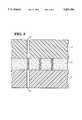
- FIG. 4is a cross-sectional view of the multi-chip module of FIG. 1.
- FIG. 5is a cross-sectional view of a multi-chip module including multiple internal layers and having MCM components packaged in a three-dimensional manner in accordance with a second embodiment of the present invention.
- Three implementations of three-dimensional MCM die packagingare presented below: (1) a single-layer common die package, (2) a dual-layer common die package, and (3) a dual-layer dissimilar die package.
- FIGS. 1 and 2illustrate a single layer common die three-dimensional package for a multi-chip module in isometric and exploded isometric views, respectively.
- the packageis seen to include a first, or upper, substrate 12 and a second, or lower substrate 14.
- Integrated circuit devices 21, 22 and 23are mounted to the top surface of upper substrate 12 using conventional mounting techniques such a TAB or BGA mounting processes.
- Integrated circuit devices 21, 22 and 23may also be electrically connected through signal paths formed on the upper surface of substrate 12 or through plated vias to signal paths residing within signal layers internal to substrate 12.
- integrated circuit devices 31 through 39are attached to the lower substrate 14 using Flip-TAB mounting techniques.
- Flip-TAB mounted devices 31 through 39reside in cavities formed into the top surface of lower substrate 14.
- Integrated circuit devices 31 through 39may be electrically connected through signal paths formed on the upper surface of substrate 14 or through plated vias and signal paths residing within signal layers internal to substrate 14.
- FIG. 4is a cross-sectional view of the multi-chip module of FIG. 1.
- the cross-sectional viewshows a portion of integrated circuit device 21 TAB mounted to the surface of upper substrate 12, and a portion of integrated circuit device 32 Flip-TAB mounted within a cavity in lower substrate 14.
- Antisotrophic material 43is provided between the upper and lower substrates, as well as between the lower substrate and printed circuit board 16.
- the thickness t S2 of lower substrate 14must be equal to the thickness of integrated circuit devices 31 through 39 embedded therein. This allows for the integrated circuit device package to make contact with thermal vias, such as via 47, on the motherboard, or on another layer of the MCM which connects to a layer possessing sufficient thermal capacity. As shown in FIG. 4, the outer signal layer of the MCM formed on the top surface of upper substrate 12, and the buried signal layer formed on the top surface of lower substrate 14, are only separated by the thickness t S1 of the upper substrate plus the thickness of the antisotrophic material.
- FIG. 5illustrates, in cross-sectional view, a three-dimensional multi-chip module package including dual internal layers in accordance with a second embodiment of the present invention.
- the three-dimensional MCM package implementation shown in FIG. 5includes an additional substrate 15, placed directly below substrate 14 which contains cavities to accommodate the integrated circuit devices attached to the bottom surface of substrate 14.
- the thickness t S3 of this layermust be equal or greater than the thickness of the integrated circuit devices attached to the bottom surface of substrate 14.
- antisotrophic material 43is used to make electrical connections between the individual substrates within the MCM as well as between the MCM and motherboard 16.
- thermal viassuch as vias 47 and 49, are provided through the motherboard and substrate 15, respectively, to make contact to the internal integrated circuit devices. This implementation yields signal path lengths equal to the thickness of the upper die only.
- the dual-layer dissimilar die MCM packageis identical to the dual-layer common die MCM package discussed above except that the thickness of substrates 12, 14 and 15, and the devices attached thereto need not be equal, i.e., t S1 ⁇ t S2 ⁇ t S3 .
- the present inventiona method for increasing the number of components within an MCM while reducing the lengths of signal paths between different points on the module.
- the three-dimensional die attachment methods described hereinoffer significantly shorter signal path lengths. This shortened path length will become more and more critical as clock speeds increase.
- An ultimate goalis to allow all busses contained in the MCM to operate at the same speed as the CPU, thereby increasing overall system throughput.
- a method for managing thermal concerns for these buried devicesis described.
Landscapes
- Engineering & Computer Science (AREA)
- Power Engineering (AREA)
- Microelectronics & Electronic Packaging (AREA)
- Physics & Mathematics (AREA)
- Condensed Matter Physics & Semiconductors (AREA)
- General Physics & Mathematics (AREA)
- Computer Hardware Design (AREA)
- Combinations Of Printed Boards (AREA)
Abstract
Description
Claims (5)
Priority Applications (1)
| Application Number | Priority Date | Filing Date | Title |
|---|---|---|---|
| US08/361,062US5495394A (en) | 1994-12-19 | 1994-12-19 | Three dimensional die packaging in multi-chip modules |
Applications Claiming Priority (1)
| Application Number | Priority Date | Filing Date | Title |
|---|---|---|---|
| US08/361,062US5495394A (en) | 1994-12-19 | 1994-12-19 | Three dimensional die packaging in multi-chip modules |
Publications (1)
| Publication Number | Publication Date |
|---|---|
| US5495394Atrue US5495394A (en) | 1996-02-27 |
Family
ID=23420496
Family Applications (1)
| Application Number | Title | Priority Date | Filing Date |
|---|---|---|---|
| US08/361,062Expired - LifetimeUS5495394A (en) | 1994-12-19 | 1994-12-19 | Three dimensional die packaging in multi-chip modules |
Country Status (1)
| Country | Link |
|---|---|
| US (1) | US5495394A (en) |
Cited By (38)
| Publication number | Priority date | Publication date | Assignee | Title |
|---|---|---|---|---|
| US5780776A (en)* | 1996-05-31 | 1998-07-14 | Nec Corporation | Multilayer circuit board unit |
| WO1999041957A1 (en)* | 1998-02-13 | 1999-08-19 | Merrimac Industries, Inc. | Method of making microwave, multifunction modules using fluoropolymer composite substrates |
| US5943216A (en)* | 1997-06-03 | 1999-08-24 | Photo Opto Electronic Technologies | Apparatus for providing a two-sided, cavity, inverted-mounted component circuit board |
| US5977640A (en)* | 1998-06-26 | 1999-11-02 | International Business Machines Corporation | Highly integrated chip-on-chip packaging |
| US6011691A (en)* | 1998-04-23 | 2000-01-04 | Lockheed Martin Corporation | Electronic component assembly and method for low cost EMI and capacitive coupling elimination |
| US6054676A (en)* | 1998-02-09 | 2000-04-25 | Kryotech, Inc. | Method and apparatus for cooling an integrated circuit device |
| US6083340A (en)* | 1997-02-28 | 2000-07-04 | Hokuriku Electric Industry Co., Ltd. | Process for manufacturing a multi-layer circuit board |
| US6212767B1 (en)* | 1999-08-31 | 2001-04-10 | Micron Technology, Inc. | Assembling a stacked die package |
| US6225699B1 (en) | 1998-06-26 | 2001-05-01 | International Business Machines Corporation | Chip-on-chip interconnections of varied characteristics |
| US6395578B1 (en) | 1999-05-20 | 2002-05-28 | Amkor Technology, Inc. | Semiconductor package and method for fabricating the same |
| US6414396B1 (en) | 2000-01-24 | 2002-07-02 | Amkor Technology, Inc. | Package for stacked integrated circuits |
| US6452278B1 (en) | 2000-06-30 | 2002-09-17 | Amkor Technology, Inc. | Low profile package for plural semiconductor dies |
| US6462976B1 (en) | 1997-02-21 | 2002-10-08 | University Of Arkansas | Conversion of electrical energy from one form to another, and its management through multichip module structures |
| US6468640B2 (en)* | 2000-04-10 | 2002-10-22 | Murata Manufacturing Co., Ltd. | Monolithic ceramic substrate, manufacturing and designing methods therefor, and electronic device |
| US20030015422A1 (en)* | 1997-04-30 | 2003-01-23 | Ingrid Fritsch | Microfabricated recessed disk microelectrodes: characterization in static and convective solutions |
| US6552416B1 (en) | 2000-09-08 | 2003-04-22 | Amkor Technology, Inc. | Multiple die lead frame package with enhanced die-to-die interconnect routing using internal lead trace wiring |
| US20030077642A1 (en)* | 2000-10-16 | 2003-04-24 | Ingrid Fritsch | Self-contained microelectrochemical bioassy platforms and methods |
| US20030199118A1 (en)* | 1999-12-20 | 2003-10-23 | Amkor Technology, Inc. | Wire bonding method for a semiconductor package |
| US20040007771A1 (en)* | 1999-08-24 | 2004-01-15 | Amkor Technology, Inc. | Semiconductor package and method for fabricating the smae |
| US20040056334A1 (en)* | 2002-09-25 | 2004-03-25 | Maxwell Electronic Components Group, Inc. | Method and apparatus for shielding an integrated circuit from radiation |
| US6717248B2 (en) | 1999-05-07 | 2004-04-06 | Amkor Technology, Inc. | Semiconductor package and method for fabricating the same |
| US6759737B2 (en) | 2000-03-25 | 2004-07-06 | Amkor Technology, Inc. | Semiconductor package including stacked chips with aligned input/output pads |
| WO2004105134A1 (en)* | 2003-05-20 | 2004-12-02 | Infineon Technologies Ag | An integrated circuit package |
| US6887714B2 (en) | 2000-10-16 | 2005-05-03 | Board Of Trustees Of The University Of Arkansas, N.A. | Microvolume immunoabsorbant assays with amplified electrochemical detection |
| US20050156322A1 (en)* | 2001-08-31 | 2005-07-21 | Smith Lee J. | Thin semiconductor package including stacked dies |
| US7144486B1 (en) | 1997-04-30 | 2006-12-05 | Board Of Trustees Of The University Of Arkansas | Multilayer microcavity devices and methods |
| US20070096267A1 (en)* | 2005-10-27 | 2007-05-03 | Hon Hai Precision Industry Co., Ltd. | Motherboard with selective chip layout |
| US20070145548A1 (en)* | 2003-12-22 | 2007-06-28 | Amkor Technology, Inc. | Stack-type semiconductor package and manufacturing method thereof |
| USRE40112E1 (en) | 1999-05-20 | 2008-02-26 | Amkor Technology, Inc. | Semiconductor package and method for fabricating the same |
| US20080192516A1 (en)* | 2005-08-23 | 2008-08-14 | Stefan Morbe | Input Circuit for a Switch-Mode Power Supply |
| US20080251895A1 (en)* | 2003-07-16 | 2008-10-16 | Janet Patterson | Apparatus for shielding integrated circuit devices |
| US7456028B2 (en) | 2000-10-16 | 2008-11-25 | Board Of Trustees Of The University Of Arkansas, N.A. | Electrochemical method for detecting water born pathogens |
| US8076177B2 (en) | 2010-05-14 | 2011-12-13 | International Business Machines Corporation | Scalable transfer-join bonding lock-and-key structures |
| WO2012058295A1 (en)* | 2010-10-26 | 2012-05-03 | Tsu-Chang Lee | Apparatus for network based modular electronic systems |
| US8378478B2 (en) | 2010-11-24 | 2013-02-19 | Tessera, Inc. | Enhanced stacked microelectronic assemblies with central contacts and vias connected to the central contacts |
| US9230726B1 (en) | 2015-02-20 | 2016-01-05 | Crane Electronics, Inc. | Transformer-based power converters with 3D printed microchannel heat sink |
| US9466545B1 (en) | 2007-02-21 | 2016-10-11 | Amkor Technology, Inc. | Semiconductor package in package |
| US9888568B2 (en) | 2012-02-08 | 2018-02-06 | Crane Electronics, Inc. | Multilayer electronics assembly and method for embedding electrical circuit components within a three dimensional module |
Citations (6)
| Publication number | Priority date | Publication date | Assignee | Title |
|---|---|---|---|---|
| JPH03152967A (en)* | 1989-11-09 | 1991-06-28 | Nec Corp | Hybrid integrated circuit device |
| JPH0418787A (en)* | 1990-03-30 | 1992-01-22 | Toshiba Corp | Printed wiring board connection device |
| US5172303A (en)* | 1990-11-23 | 1992-12-15 | Motorola, Inc. | Electronic component assembly |
| US5241456A (en)* | 1990-07-02 | 1993-08-31 | General Electric Company | Compact high density interconnect structure |
| US5290971A (en)* | 1990-12-04 | 1994-03-01 | Mitsubishi Denki Kabushiki Kaisha | Printed circuit board provided with a higher density of terminals for hybrid integrated circuit and method of fabricating the same |
| US5371654A (en)* | 1992-10-19 | 1994-12-06 | International Business Machines Corporation | Three dimensional high performance interconnection package |
- 1994
- 1994-12-19USUS08/361,062patent/US5495394A/ennot_activeExpired - Lifetime
Patent Citations (6)
| Publication number | Priority date | Publication date | Assignee | Title |
|---|---|---|---|---|
| JPH03152967A (en)* | 1989-11-09 | 1991-06-28 | Nec Corp | Hybrid integrated circuit device |
| JPH0418787A (en)* | 1990-03-30 | 1992-01-22 | Toshiba Corp | Printed wiring board connection device |
| US5241456A (en)* | 1990-07-02 | 1993-08-31 | General Electric Company | Compact high density interconnect structure |
| US5172303A (en)* | 1990-11-23 | 1992-12-15 | Motorola, Inc. | Electronic component assembly |
| US5290971A (en)* | 1990-12-04 | 1994-03-01 | Mitsubishi Denki Kabushiki Kaisha | Printed circuit board provided with a higher density of terminals for hybrid integrated circuit and method of fabricating the same |
| US5371654A (en)* | 1992-10-19 | 1994-12-06 | International Business Machines Corporation | Three dimensional high performance interconnection package |
Cited By (66)
| Publication number | Priority date | Publication date | Assignee | Title |
|---|---|---|---|---|
| US5780776A (en)* | 1996-05-31 | 1998-07-14 | Nec Corporation | Multilayer circuit board unit |
| US6462976B1 (en) | 1997-02-21 | 2002-10-08 | University Of Arkansas | Conversion of electrical energy from one form to another, and its management through multichip module structures |
| US6083340A (en)* | 1997-02-28 | 2000-07-04 | Hokuriku Electric Industry Co., Ltd. | Process for manufacturing a multi-layer circuit board |
| US7169272B2 (en) | 1997-04-30 | 2007-01-30 | Board Of Trustees Of The University Of Arkansas | Microfabricated recessed disk microelectrodes: characterization in static and convective solutions |
| US20030015422A1 (en)* | 1997-04-30 | 2003-01-23 | Ingrid Fritsch | Microfabricated recessed disk microelectrodes: characterization in static and convective solutions |
| US7144486B1 (en) | 1997-04-30 | 2006-12-05 | Board Of Trustees Of The University Of Arkansas | Multilayer microcavity devices and methods |
| US5943216A (en)* | 1997-06-03 | 1999-08-24 | Photo Opto Electronic Technologies | Apparatus for providing a two-sided, cavity, inverted-mounted component circuit board |
| US6054676A (en)* | 1998-02-09 | 2000-04-25 | Kryotech, Inc. | Method and apparatus for cooling an integrated circuit device |
| US6099677A (en)* | 1998-02-13 | 2000-08-08 | Merrimac Industries, Inc. | Method of making microwave, multifunction modules using fluoropolymer composite substrates |
| WO1999041957A1 (en)* | 1998-02-13 | 1999-08-19 | Merrimac Industries, Inc. | Method of making microwave, multifunction modules using fluoropolymer composite substrates |
| US6395374B1 (en) | 1998-02-13 | 2002-05-28 | Merrimac Industries, Inc. | Method of making microwave, multifunction modules using fluoropolymer composite substrates |
| US6011691A (en)* | 1998-04-23 | 2000-01-04 | Lockheed Martin Corporation | Electronic component assembly and method for low cost EMI and capacitive coupling elimination |
| US6294406B1 (en) | 1998-06-26 | 2001-09-25 | International Business Machines Corporation | Highly integrated chip-on-chip packaging |
| US6225699B1 (en) | 1998-06-26 | 2001-05-01 | International Business Machines Corporation | Chip-on-chip interconnections of varied characteristics |
| US5977640A (en)* | 1998-06-26 | 1999-11-02 | International Business Machines Corporation | Highly integrated chip-on-chip packaging |
| US6642080B1 (en) | 1998-06-26 | 2003-11-04 | International Business Machines Corporation | Chip-on-chip interconnections of varied characterstics |
| US6717248B2 (en) | 1999-05-07 | 2004-04-06 | Amkor Technology, Inc. | Semiconductor package and method for fabricating the same |
| US7190071B2 (en) | 1999-05-07 | 2007-03-13 | Amkor Technology, Inc. | Semiconductor package and method for fabricating the same |
| US20040164411A1 (en)* | 1999-05-07 | 2004-08-26 | Amkor Technology, Inc. | Semiconductor package and method for fabricating the same |
| US20040175916A1 (en)* | 1999-05-20 | 2004-09-09 | Amkor Technology, Inc. | Stackable semiconductor package having semiconductor chip within central through hole of substrate |
| US6762078B2 (en) | 1999-05-20 | 2004-07-13 | Amkor Technology, Inc. | Semiconductor package having semiconductor chip within central aperture of substrate |
| USRE40112E1 (en) | 1999-05-20 | 2008-02-26 | Amkor Technology, Inc. | Semiconductor package and method for fabricating the same |
| US7061120B2 (en) | 1999-05-20 | 2006-06-13 | Amkor Technology, Inc. | Stackable semiconductor package having semiconductor chip within central through hole of substrate |
| US6395578B1 (en) | 1999-05-20 | 2002-05-28 | Amkor Technology, Inc. | Semiconductor package and method for fabricating the same |
| US20050205979A1 (en)* | 1999-08-24 | 2005-09-22 | Shin Won S | Semiconductor package and method for fabricating the same |
| US20040007771A1 (en)* | 1999-08-24 | 2004-01-15 | Amkor Technology, Inc. | Semiconductor package and method for fabricating the smae |
| US6982488B2 (en) | 1999-08-24 | 2006-01-03 | Amkor Technology, Inc. | Semiconductor package and method for fabricating the same |
| US7211900B2 (en) | 1999-08-24 | 2007-05-01 | Amkor Technology, Inc. | Thin semiconductor package including stacked dies |
| US6212767B1 (en)* | 1999-08-31 | 2001-04-10 | Micron Technology, Inc. | Assembling a stacked die package |
| US20030199118A1 (en)* | 1999-12-20 | 2003-10-23 | Amkor Technology, Inc. | Wire bonding method for a semiconductor package |
| US6803254B2 (en) | 1999-12-20 | 2004-10-12 | Amkor Technology, Inc. | Wire bonding method for a semiconductor package |
| US6642610B2 (en) | 1999-12-20 | 2003-11-04 | Amkor Technology, Inc. | Wire bonding method and semiconductor package manufactured using the same |
| US6414396B1 (en) | 2000-01-24 | 2002-07-02 | Amkor Technology, Inc. | Package for stacked integrated circuits |
| US6759737B2 (en) | 2000-03-25 | 2004-07-06 | Amkor Technology, Inc. | Semiconductor package including stacked chips with aligned input/output pads |
| US6468640B2 (en)* | 2000-04-10 | 2002-10-22 | Murata Manufacturing Co., Ltd. | Monolithic ceramic substrate, manufacturing and designing methods therefor, and electronic device |
| US6452278B1 (en) | 2000-06-30 | 2002-09-17 | Amkor Technology, Inc. | Low profile package for plural semiconductor dies |
| US6552416B1 (en) | 2000-09-08 | 2003-04-22 | Amkor Technology, Inc. | Multiple die lead frame package with enhanced die-to-die interconnect routing using internal lead trace wiring |
| US7348183B2 (en) | 2000-10-16 | 2008-03-25 | Board Of Trustees Of The University Of Arkansas | Self-contained microelectrochemical bioassay platforms and methods |
| US6887714B2 (en) | 2000-10-16 | 2005-05-03 | Board Of Trustees Of The University Of Arkansas, N.A. | Microvolume immunoabsorbant assays with amplified electrochemical detection |
| US7456028B2 (en) | 2000-10-16 | 2008-11-25 | Board Of Trustees Of The University Of Arkansas, N.A. | Electrochemical method for detecting water born pathogens |
| US20030077642A1 (en)* | 2000-10-16 | 2003-04-24 | Ingrid Fritsch | Self-contained microelectrochemical bioassy platforms and methods |
| US20050156322A1 (en)* | 2001-08-31 | 2005-07-21 | Smith Lee J. | Thin semiconductor package including stacked dies |
| US20040056334A1 (en)* | 2002-09-25 | 2004-03-25 | Maxwell Electronic Components Group, Inc. | Method and apparatus for shielding an integrated circuit from radiation |
| US7382043B2 (en) | 2002-09-25 | 2008-06-03 | Maxwell Technologies, Inc. | Method and apparatus for shielding an integrated circuit from radiation |
| US8102041B2 (en) | 2003-05-20 | 2012-01-24 | Infineon Technologies Ag | Integrated circuit package |
| US20060068523A1 (en)* | 2003-05-20 | 2006-03-30 | Infineon Technologies Ag | Integrated circuit package |
| WO2004105134A1 (en)* | 2003-05-20 | 2004-12-02 | Infineon Technologies Ag | An integrated circuit package |
| US20100207267A1 (en)* | 2003-05-20 | 2010-08-19 | Tiang Hock Lin | Integrated Circuit Package |
| US7727799B2 (en) | 2003-05-20 | 2010-06-01 | Infineon Technologies Ag | Integrated circuit package |
| US8018739B2 (en) | 2003-07-16 | 2011-09-13 | Maxwell Technologies, LLC | Apparatus for shielding integrated circuit devices |
| US20080251895A1 (en)* | 2003-07-16 | 2008-10-16 | Janet Patterson | Apparatus for shielding integrated circuit devices |
| US20100155912A1 (en)* | 2003-07-16 | 2010-06-24 | Maxwell Technologies, Inc. | Apparatus for shielding integrated circuit devices |
| US7696610B2 (en) | 2003-07-16 | 2010-04-13 | Maxwell Technologies, Inc. | Apparatus for shielding integrated circuit devices |
| US20070145548A1 (en)* | 2003-12-22 | 2007-06-28 | Amkor Technology, Inc. | Stack-type semiconductor package and manufacturing method thereof |
| US20080192516A1 (en)* | 2005-08-23 | 2008-08-14 | Stefan Morbe | Input Circuit for a Switch-Mode Power Supply |
| US8072783B2 (en)* | 2005-08-23 | 2011-12-06 | Power Systems Technologies Gmbh | Input circuit for a switch-mode power supply |
| US20070096267A1 (en)* | 2005-10-27 | 2007-05-03 | Hon Hai Precision Industry Co., Ltd. | Motherboard with selective chip layout |
| US9466545B1 (en) | 2007-02-21 | 2016-10-11 | Amkor Technology, Inc. | Semiconductor package in package |
| US9768124B2 (en) | 2007-02-21 | 2017-09-19 | Amkor Technology, Inc. | Semiconductor package in package |
| US8076177B2 (en) | 2010-05-14 | 2011-12-13 | International Business Machines Corporation | Scalable transfer-join bonding lock-and-key structures |
| WO2012058295A1 (en)* | 2010-10-26 | 2012-05-03 | Tsu-Chang Lee | Apparatus for network based modular electronic systems |
| US20130215069A1 (en)* | 2010-10-26 | 2013-08-22 | Tsu-Chang Lee | Apparatus for network based modular electronic systems |
| US8378478B2 (en) | 2010-11-24 | 2013-02-19 | Tessera, Inc. | Enhanced stacked microelectronic assemblies with central contacts and vias connected to the central contacts |
| US9888568B2 (en) | 2012-02-08 | 2018-02-06 | Crane Electronics, Inc. | Multilayer electronics assembly and method for embedding electrical circuit components within a three dimensional module |
| US11172572B2 (en) | 2012-02-08 | 2021-11-09 | Crane Electronics, Inc. | Multilayer electronics assembly and method for embedding electrical circuit components within a three dimensional module |
| US9230726B1 (en) | 2015-02-20 | 2016-01-05 | Crane Electronics, Inc. | Transformer-based power converters with 3D printed microchannel heat sink |
Similar Documents
| Publication | Publication Date | Title |
|---|---|---|
| US5495394A (en) | Three dimensional die packaging in multi-chip modules | |
| US5444296A (en) | Ball grid array packages for high speed applications | |
| US5391917A (en) | Multiprocessor module packaging | |
| US5426566A (en) | Multichip integrated circuit packages and systems | |
| EP0683968B1 (en) | Module comprising ic memory stack dedicated to and structurally combined with an ic microprocessor | |
| US5801072A (en) | Method of packaging integrated circuits | |
| US5838545A (en) | High performance, low cost multi-chip modle package | |
| US6229216B1 (en) | Silicon interposer and multi-chip-module (MCM) with through substrate vias | |
| US6266246B1 (en) | Multi-chip module having interconnect dies | |
| US7279795B2 (en) | Stacked die semiconductor package | |
| US5793115A (en) | Three dimensional processor using transferred thin film circuits | |
| US6043559A (en) | Integrated circuit package which contains two in plane voltage busses and a wrap around conductive strip that connects a bond finger to one of the busses | |
| JP2001244406A (en) | High-performance multi-chip ic package | |
| JP2003060153A (en) | Semiconductor package | |
| US5832294A (en) | Multiple-microprocessor module | |
| US5719745A (en) | Extended surface cooling for chip stack applications | |
| Akihiro et al. | Packaging technology for the NEC SX-3/SX-X supercomputer | |
| US6541847B1 (en) | Packaging for multi-processor shared-memory system | |
| US20240290682A1 (en) | Package structure with buffer layer embedded in lid layer | |
| US6008988A (en) | Integrated circuit package with a heat spreader coupled to a pair of electrical devices | |
| US6326686B1 (en) | Vertical semiconductor device package having printed circuit board and heat spreader, and module having the packages | |
| US6627978B2 (en) | Chip package enabling increased input/output density | |
| US6973715B2 (en) | Method of forming a multichip module having chips on two sides | |
| US6952352B2 (en) | Integrated circuit chip package with formable intermediate 3D wiring structure | |
| US6057594A (en) | High power dissipating tape ball grid array package |
Legal Events
| Date | Code | Title | Description |
|---|---|---|---|
| AS | Assignment | Owner name:AT&T GLOBAL INFORMATION SOLUTIONS COMPANY, OHIO Free format text:ASSIGNMENT OF ASSIGNORS INTEREST;ASSIGNORS:KORNFELD, BRUCE E.;ALEXANDER, ARTHUR R.;REEL/FRAME:007284/0242;SIGNING DATES FROM 19941202 TO 19941209 | |
| STCF | Information on status: patent grant | Free format text:PATENTED CASE | |
| AS | Assignment | Owner name:NCR CORPORATION, OHIO Free format text:ASSIGNMENT OF ASSIGNORS INTEREST;ASSIGNOR:AT&T GLOBAL INFORMATION SOLUTIONS COMPANY;REEL/FRAME:008047/0429 Effective date:19960109 | |
| FPAY | Fee payment | Year of fee payment:4 | |
| FPAY | Fee payment | Year of fee payment:8 | |
| AS | Assignment | Owner name:STEINMETZ ELECTRICAL LLC, CALIFORNIA Free format text:ASSIGNMENT OF ASSIGNORS INTEREST;ASSIGNOR:NCR CORPORATION;REEL/FRAME:015428/0845 Effective date:20040623 | |
| FPAY | Fee payment | Year of fee payment:12 | |
| FEPP | Fee payment procedure | Free format text:PAYOR NUMBER ASSIGNED (ORIGINAL EVENT CODE: ASPN); ENTITY STATUS OF PATENT OWNER: LARGE ENTITY Free format text:PAYER NUMBER DE-ASSIGNED (ORIGINAL EVENT CODE: RMPN); ENTITY STATUS OF PATENT OWNER: LARGE ENTITY | |
| AS | Assignment | Owner name:INTELLECTUAL VENTURES I LLC, DELAWARE Free format text:MERGER;ASSIGNOR:STEINMETZ ELECTRICAL LLC;REEL/FRAME:025467/0109 Effective date:20101207 |