US5494698A - Teflon filled resinoid dicing blades for fabricating silicon die modules - Google Patents
Teflon filled resinoid dicing blades for fabricating silicon die modulesDownload PDFInfo
- Publication number
- US5494698A US5494698AUS08/334,978US33497894AUS5494698AUS 5494698 AUS5494698 AUS 5494698AUS 33497894 AUS33497894 AUS 33497894AUS 5494698 AUS5494698 AUS 5494698A
- Authority
- US
- United States
- Prior art keywords
- blade
- resinoid
- teflon
- dicing
- solution
- Prior art date
- Legal status (The legal status is an assumption and is not a legal conclusion. Google has not performed a legal analysis and makes no representation as to the accuracy of the status listed.)
- Expired - Lifetime
Links
- 229920006362Teflon®Polymers0.000titleclaimsabstractdescription44
- 229910052710siliconInorganic materials0.000titleabstractdescription24
- 239000010703siliconSubstances0.000titleabstractdescription24
- XUIMIQQOPSSXEZ-UHFFFAOYSA-NSiliconChemical compound[Si]XUIMIQQOPSSXEZ-UHFFFAOYSA-N0.000titleabstractdescription23
- 239000004809TeflonSubstances0.000titledescription17
- 238000000034methodMethods0.000claimsabstractdescription18
- 239000002904solventSubstances0.000claimsdescription12
- 239000011148porous materialSubstances0.000claimsdescription9
- 229920001343polytetrafluoroethylenePolymers0.000claimsdescription8
- 239000004810polytetrafluoroethyleneSubstances0.000claimsdescription8
- -1polytetrafluoroethylenePolymers0.000claimsdescription7
- YVBBRRALBYAZBM-UHFFFAOYSA-NperfluorooctaneChemical compoundFC(F)(F)C(F)(F)C(F)(F)C(F)(F)C(F)(F)C(F)(F)C(F)(F)C(F)(F)FYVBBRRALBYAZBM-UHFFFAOYSA-N0.000claimsdescription4
- 239000011521glassSubstances0.000claimsdescription3
- 239000000203mixtureSubstances0.000claimsdescription3
- 238000005096rolling processMethods0.000claimsdescription3
- 230000002745absorbentEffects0.000claimsdescription2
- 239000002250absorbentSubstances0.000claimsdescription2
- 238000001704evaporationMethods0.000claims2
- 238000001035dryingMethods0.000claims1
- 230000008020evaporationEffects0.000claims1
- 239000007787solidSubstances0.000claims1
- 235000012431wafersNutrition0.000abstractdescription46
- 238000010438heat treatmentMethods0.000description14
- 238000005520cutting processMethods0.000description7
- 239000010432diamondSubstances0.000description7
- 239000000758substrateSubstances0.000description7
- 229910003460diamondInorganic materials0.000description6
- 239000000463materialSubstances0.000description6
- 230000035515penetrationEffects0.000description6
- 239000011347resinSubstances0.000description4
- 229920005989resinPolymers0.000description4
- 238000004519manufacturing processMethods0.000description3
- 238000000926separation methodMethods0.000description3
- 239000002210silicon-based materialSubstances0.000description3
- 239000004642PolyimideSubstances0.000description2
- 239000002826coolantSubstances0.000description2
- 238000001816coolingMethods0.000description2
- 230000037406food intakeEffects0.000description2
- 239000004615ingredientSubstances0.000description2
- 238000012986modificationMethods0.000description2
- 230000004048modificationEffects0.000description2
- RVZRBWKZFJCCIB-UHFFFAOYSA-NperfluorotributylamineChemical compoundFC(F)(F)C(F)(F)C(F)(F)C(F)(F)N(C(F)(F)C(F)(F)C(F)(F)C(F)(F)F)C(F)(F)C(F)(F)C(F)(F)C(F)(F)FRVZRBWKZFJCCIB-UHFFFAOYSA-N0.000description2
- 229920001721polyimidePolymers0.000description2
- 229910000859α-FeInorganic materials0.000description2
- 208000032544CicatrixDiseases0.000description1
- 241000763859Dyckia brevifoliaSpecies0.000description1
- 238000005299abrasionMethods0.000description1
- 230000004308accommodationEffects0.000description1
- 239000000853adhesiveSubstances0.000description1
- 238000004026adhesive bondingMethods0.000description1
- 230000001070adhesive effectEffects0.000description1
- 238000003491arrayMethods0.000description1
- 239000012298atmosphereSubstances0.000description1
- 230000015572biosynthetic processEffects0.000description1
- 230000005587bubblingEffects0.000description1
- BGTFCAQCKWKTRL-YDEUACAXSA-Nchembl1095986Chemical compoundC1[C@@H](N)[C@@H](O)[C@H](C)O[C@H]1O[C@@H]([C@H]1C(N[C@H](C2=CC(O)=CC(O[C@@H]3[C@H]([C@@H](O)[C@H](O)[C@@H](CO)O3)O)=C2C=2C(O)=CC=C(C=2)[C@@H](NC(=O)[C@@H]2NC(=O)[C@@H]3C=4C=C(C(=C(O)C=4)C)OC=4C(O)=CC=C(C=4)[C@@H](N)C(=O)N[C@@H](C(=O)N3)[C@H](O)C=3C=CC(O4)=CC=3)C(=O)N1)C(O)=O)=O)C(C=C1)=CC=C1OC1=C(O[C@@H]3[C@H]([C@H](O)[C@@H](O)[C@H](CO[C@@H]5[C@H]([C@@H](O)[C@H](O)[C@@H](C)O5)O)O3)O[C@@H]3[C@H]([C@@H](O)[C@H](O)[C@@H](CO)O3)O[C@@H]3[C@H]([C@H](O)[C@@H](CO)O3)O)C4=CC2=C1BGTFCAQCKWKTRL-YDEUACAXSA-N0.000description1
- 239000003795chemical substances by applicationSubstances0.000description1
- 239000013078crystalSubstances0.000description1
- 230000001419dependent effectEffects0.000description1
- 238000005530etchingMethods0.000description1
- 239000000945fillerSubstances0.000description1
- 239000012530fluidSubstances0.000description1
- 238000007641inkjet printingMethods0.000description1
- 238000002156mixingMethods0.000description1
- 238000013021overheatingMethods0.000description1
- 239000002245particleSubstances0.000description1
- 238000002161passivationMethods0.000description1
- 238000005498polishingMethods0.000description1
- 229920000642polymerPolymers0.000description1
- 239000013557residual solventSubstances0.000description1
- 231100000241scarToxicity0.000description1
- 230000037390scarringEffects0.000description1
- 230000037387scarsEffects0.000description1
- 150000003376siliconChemical class0.000description1
- XLYOFNOQVPJJNP-UHFFFAOYSA-NwaterSubstancesOXLYOFNOQVPJJNP-UHFFFAOYSA-N0.000description1
Images


Classifications
- B—PERFORMING OPERATIONS; TRANSPORTING
- B05—SPRAYING OR ATOMISING IN GENERAL; APPLYING FLUENT MATERIALS TO SURFACES, IN GENERAL
- B05D—PROCESSES FOR APPLYING FLUENT MATERIALS TO SURFACES, IN GENERAL
- B05D3/00—Pretreatment of surfaces to which liquids or other fluent materials are to be applied; After-treatment of applied coatings, e.g. intermediate treating of an applied coating preparatory to subsequent applications of liquids or other fluent materials
- B05D3/04—Pretreatment of surfaces to which liquids or other fluent materials are to be applied; After-treatment of applied coatings, e.g. intermediate treating of an applied coating preparatory to subsequent applications of liquids or other fluent materials by exposure to gases
- B05D3/0493—Pretreatment of surfaces to which liquids or other fluent materials are to be applied; After-treatment of applied coatings, e.g. intermediate treating of an applied coating preparatory to subsequent applications of liquids or other fluent materials by exposure to gases using vacuum
- B—PERFORMING OPERATIONS; TRANSPORTING
- B05—SPRAYING OR ATOMISING IN GENERAL; APPLYING FLUENT MATERIALS TO SURFACES, IN GENERAL
- B05D—PROCESSES FOR APPLYING FLUENT MATERIALS TO SURFACES, IN GENERAL
- B05D1/00—Processes for applying liquids or other fluent materials
- B05D1/18—Processes for applying liquids or other fluent materials performed by dipping
- B—PERFORMING OPERATIONS; TRANSPORTING
- B23—MACHINE TOOLS; METAL-WORKING NOT OTHERWISE PROVIDED FOR
- B23D—PLANING; SLOTTING; SHEARING; BROACHING; SAWING; FILING; SCRAPING; LIKE OPERATIONS FOR WORKING METAL BY REMOVING MATERIAL, NOT OTHERWISE PROVIDED FOR
- B23D61/00—Tools for sawing machines or sawing devices; Clamping devices for these tools
- B23D61/02—Circular saw blades
- B23D61/10—Circular saw blades clamped between hubs; Clamping or aligning devices therefor
- B—PERFORMING OPERATIONS; TRANSPORTING
- B23—MACHINE TOOLS; METAL-WORKING NOT OTHERWISE PROVIDED FOR
- B23D—PLANING; SLOTTING; SHEARING; BROACHING; SAWING; FILING; SCRAPING; LIKE OPERATIONS FOR WORKING METAL BY REMOVING MATERIAL, NOT OTHERWISE PROVIDED FOR
- B23D65/00—Making tools for sawing machines or sawing devices for use in cutting any kind of material
- B—PERFORMING OPERATIONS; TRANSPORTING
- B24—GRINDING; POLISHING
- B24D—TOOLS FOR GRINDING, BUFFING OR SHARPENING
- B24D3/00—Physical features of abrasive bodies, or sheets, e.g. abrasive surfaces of special nature; Abrasive bodies or sheets characterised by their constituents
- B24D3/34—Physical features of abrasive bodies, or sheets, e.g. abrasive surfaces of special nature; Abrasive bodies or sheets characterised by their constituents characterised by additives enhancing special physical properties, e.g. wear resistance, electric conductivity, self-cleaning properties
- B—PERFORMING OPERATIONS; TRANSPORTING
- B24—GRINDING; POLISHING
- B24D—TOOLS FOR GRINDING, BUFFING OR SHARPENING
- B24D5/00—Bonded abrasive wheels, or wheels with inserted abrasive blocks, designed for acting only by their periphery; Bushings or mountings therefor
- B24D5/12—Cut-off wheels
- B—PERFORMING OPERATIONS; TRANSPORTING
- B28—WORKING CEMENT, CLAY, OR STONE
- B28D—WORKING STONE OR STONE-LIKE MATERIALS
- B28D5/00—Fine working of gems, jewels, crystals, e.g. of semiconductor material; apparatus or devices therefor
- B28D5/02—Fine working of gems, jewels, crystals, e.g. of semiconductor material; apparatus or devices therefor by rotary tools, e.g. drills
- B28D5/022—Fine working of gems, jewels, crystals, e.g. of semiconductor material; apparatus or devices therefor by rotary tools, e.g. drills by cutting with discs or wheels
Definitions
- This inventionrelates to dicing of silicon die modules, such as, for example, an ink jet printhead, and more particularly to dicing silicon die with an improved resinoid dicing blade having Teflon® impregnated therein and method of impregnating the resinoid dicing blades with Teflon®,the improved dicing blade being used to separate die modules for a pair of bonded silicon wafers.
- U.S. Pat. No. Re 32,572 to Hawkins et al.discloses a thermal ink jet printhead and several fabricating processes therefor.
- Each printheadis composed of two parts aligned and bonded together.
- One partis a substantially flat substrate which contains on the surface thereof a linear array of heating elements and addressing electrodes
- the second partis a substrate having at least one recess anisotropically etched therein to serve as an ink supply manifold when the two parts are bonded together.
- a linear array of parallel groovesare also formed in the second part, so that one end of the grooves communicate with the manifold recess and the other ends are open for use as ink droplet expelling nozzles.
- printheadscan be made simultaneously by producing a plurality of sets of heating element arrays with their addressing electrodes on a silicon wafer and by placing alignment marks thereon at predetermined locations.
- a corresponding plurality of sets of channel grooves and associated manifoldsare produced in a second silicon wafer.
- alignment openingsare etched in the second silicon wafer at predetermined locations. The two wafers are aligned via the alignment openings and alignment marks, then bonded together and diced into many separate printheads.
- U.S. Pat. No. 4,638,337 to Torpey et al.discloses an improved thermal ink jet printhead similar to that of Hawkins et al., but has each of its heating elements located in a recess.
- the recess walls containing the heating elementsprevent the lateral movement of the bubbles through the nozzle and therefore the sudden release of vaporized ink to the atmosphere, known as blow-out, which causes ingestion of air and interrupts the printhead operation whenever this event occurs.
- a thick film organic structuresuch as Riston® or Vacrel® is interposed between the heater plate and the channel plate.
- the purpose of this layeris to have recesses formed therein directly above the heating elements to contain the bubble which is formed over the heating elements, thus enabling an increase in the droplet velocity without the occurrence of vapor blow-out and concomitant air ingestion.
- U.S. Pat. No. 4,097,310 to Lindmayerdiscloses a method of forming silicon solar cells by forming an electron generating junction on a single crystal wafer followed by a diamond blade cut through the wafer. Rotation speeds for the diamond blade fall into the range of 5,000 to 20,000 rpm with a corresponding cutting speed of 0.05 to 10 inches per second.
- U.S. Pat. No. 4,564,000 to Stern et al.discloses a method of cutting ferrite materials using a resin bonded diamond sawblade at a cutting speed of 5400 centimeters per second.
- the bladeitself has a diameter of 2.25 inches. Cooling means are applied to the blade to prevent overheating of the blade and the ferrite.
- U.S. Pat. No. 4,633,847 to Lossl et al.discloses a multiple-blade internal hole sawing method for cutting crystal-line rods into thin wafers while maintaining a connection between adjacent cut wafers.
- the waferscan be cut into thicknesses ranging from 0.1 mm to 1.0 mm.
- Connecting agentssuch as wax, are used to mechanically connect the cut wafers but can easily be removed by solvent or heating
- U.S. Pat. No. 4,878,992 to Campanellidiscloses an ink jet printhead fabrication process wherein a plurality of printheads are produced from two mated substrates by two dicing operations.
- One dicing operationproduces the nozzle face for each of a plurality of printheads and optionally produces the nozzles.
- This dicing bladetogether with specific operating parameters, reduces chipping from the nozzles, and scratches and abrasions from the nozzle faces.
- a second dicing operation with a standard dicing bladesevers the mated substrates into separate printheads.
- the dicing operation which produces the nozzle faceis preferably conducted in a two-step operation.
- a first cutmakes the nozzle face, but does not sever the two mated substrates.
- a second dicing cutsevers the two substrates, but does so in a manner that prevents contact by the dicing blade with the nozzle face.
- Micro-electromechanical systemsare generally produced by the bonding of two silicon wafers by a thick film layer, such as polyimide.
- a thick film layersuch as polyimide.
- One of the silicon surfaces covered by the thiclc film layerhas electrical circuitry thereon and and the thick film layer may be patterned to provide recesses for fluid flow or the accommodation of other micro-sized devices therein.
- a plurality of MEMS die modulesare in one silicon wafer pair which is diced into a plurality of individual die modules.
- a thermal ink jet printheadis a specific example of a MEMS die module, and a reduction in scarring and chipping is especially useful when the separation of the printhead die currently produces the printhead nozzle faces.
- ink jet printheadsare fabricated from two silicon wafers, one of which contains recesses in the confronting surface thereof. When the wafers are aligned and bonded together, the recesses form ink channels and reservoirs. Dicing the two wafers separates the printheads and concurrently opens one end of the ink channels creating the nozzles in a nozzle face.
- the dicing blade and dicing procedure of U.S. Pat. No. 4,878,992improved the yield of printheads, but some nozzle chipping remained a serious problem.
- a plurality of silicon die modulesare produced by dicing two bonded silicon wafers with a Teflon® impregnated resinoid dicing blade.
- Teflon®is impregnated into resinoid dicing blades having approximately a 20% by volume structure by immersing them into a solution comprising 2% by weight Teflon AF® the generic composition being amorphous polytetrafluoroethylene dissolved in a solvent, such as TC-75 by the 3M Company.
- the Teflon® solution with the dicing blades immersed thereinis placed into an evacuation chamber and a vacuum is drawn. When air from the exposed pores in the dicing blades are removed, the chamber is returned to atmospheric pressure.
- the dicing bladesare removed from the Teflon® solution and drained of excess Teflon® solution and dried by allowing the residual solvent to evaporate.
- the Teflon® impregnated dicing bladeshave about 0.3 to 0.5% by weight Teflon.
- the bonded wafer pair containing the plurality of printheadsis notched by dicing on opposite exposed surfaces along the dicing lines or streets which separate the printheads, so that the final separating dicing cut by the Teflon® filled or impregnated resinoid dicing blade cuts the wafer between aligned notches.
- Thisenables the nozzle faces to be produced by the Teflon® impregnated blade with a minimum of silicon material to sever and without causing the blade to contact the sticky material holding the wafer pair on the dicing frame, thus increasing the blade life.
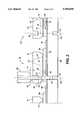
- FIG. 1is an enlarged isometric view of the channel wafer bonded to the heating element wafer, after the excess channel wafer material has been removed to expose the addressing electrode terminals, and showing the dicing blade of the present invention as it forms the nozzle containing surfaces of the printheads.
- FIG. 2is an enlarged partially shown cross sectional view of FIG. 1 taken along a plane including the dicing blade axis of rotation and blade portion along a radius located normal to the wafers.
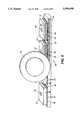
- FIG. 3is a cross sectional view of the dicing blade of the present invention in a blade holder or flange.
- FIG. 4is a partial, cross sectional isometric view of FIG. 1 showing the formation of the nozzle containing surface.
- a Teflon® filled or impregnated resin-based dicing blade 10 of the present inventionis shown cutting along a previously diced notch 30, that is located across an edge of the channel plates 31, and in the direction of arrow 13 to form the nozzles 27 and nozzle face 29 (see FIGS. 2 and 4) for the plurality of printheads 12.
- the notches 30are diced along the dicing lines 18 (shown in dashed line) between the plurality of printhead die 12 in the bonded wafers.
- Notch 30is diced in the channel wafer, while a similar notch 35 is diced in the heater wafer, so that the notches 30,35 are aligned to reduce the silicon material therebetween (Refer to FIGS. 2 and 4). Also, prior to the separating dicing cut and after the notches are formed, excess silicon material is milled from the silicon channel wafer or upper substrate to form the individual channel plates 31 and uncover the addressing electrode terminals 32. As disclosed in U.S. Pat. No. 4,638,337 to Torpey et al. and incorporated herein by reference, etched grooves and recesses (not shown) around the periphery of the channel plates 31 greatly assist in preventing damage to the addressing electrodes 33 and their terminals 32 during this silicon removal step by spacing the channel wafer therefrom.
- a thick film polymer layer 58preferably polyimide, is sandwiched between the channel plates 31 and the heater wafer 36 and is etched to remove it from the distal ends of the electrodes 33 and their contact pads or terminals 32.
- Each channel platehas an inlet 25 which may be separately etched in the channel plates or they may be simply formed by etching the manifold 22 (see FIG. 1) completely through the channel wafer from which the channel plates 31 are formed.
- the resinoid dicing blade 10is rotated about axis 11.
- the speedmay range from 20,000 to 60,000 rpm.
- the bladehas a relatively hard, porous resin bonded base material with substantially no abrasive fillers and contains a 60 to 90% concentration of natural or synthetic diamonds having a nominal diamond size range of 2 to 6 micrometers.
- the density referenceis based in 72 carats per cubic inch.
- the porosity of the resinoid dicing bladeis approximately 20% by volume, and has Teflon AF® impregnated therein by a process discussed later.
- the Teflon® filled or impregnated dicing bladescontain about 0.3 to 0.5% Teflon® by weight.
- the dicing cut to provide the nozzle containing surface with the appropriate surface finish and optionally to open the nozzlesis made along the notches 30,35.
- FIG. 2is a cross sectional view of FIG. 1 as viewed along view line 2--2 and shows that the dicing blade 10 cuts through the channel plates 31, thick film layer 58, adhesive bonding layer 15, electrode insulating underglaze layer 17, passivation layer (not shown), and into the heating element wafer 36 for the distance required to meet the notch 35.
- the blade penetration depth versus blade width ratiofalls within the range of 6:1 to 9:1. If the ratio is 10:1 or higher, the blade will wander, thus eliminating the saw cut's positional accuracy of ⁇ 0.1 mils. A high ratio also deleteriously affects nozzle surface quality.
- the ink channel 21, manifolds or reservoirs 22, and heating elements 34, shown in pits or recesses 26 in the thick film layer 58are shown in dashed line for reference to the notches 30 and 35 which are centered on dicing cut centerline 18.
- the dicing blade 10only cuts between notches 30,35 in the channel plates and heater wafer, respectively, it could completely cut through both the channel plates 31 and heating element wafer 36.
- the penalty for this complete cut throughis a shorter life of the resin bonded blade. The shorter life is caused by the adhesive used to hold the heating element wafer 36 to a standard wafer holding film frame (not shown).
- Xthe blade exposure minus the penetration depth referred to in FIG. 2 as "X".
- the value "X"must fall into the range of 6 to 12 mils. Less than 6 mils, clearance and coolant cannot get to the blade. This causes high friction resulting in a stressed cut and subsequent nozzle damage. More than 12 mils clearance and the blade vibrates and damages the nozzle and scars the nozzle face 29.
- FIG. 4is an isometric view of the heating element wafer 36 and the channel plates 31 bonded thereto as viewed along view line 4--4 of FIG. 1.
- dicing blade 10 of the present inventioncuts along cutting line 18, which is in the center of the notches 30,35, nozzles 27 and nozzle containing surface 29 are formed and the heating element wafer is severed in parallel strips.
- a second dicing cut along dicing line 23, which are perpendicular to dicing cut lines 18,completes the separation of printhead die from the originally bonded wafer pair.
- FIG. 3is a schematic cross sectional view of a typical dicing blade holder or flange assembly 38 which comprises inner flange 40 and outer flange 42 between which the dicing blade 10 is held on the circular shoulder 43 of inner flange 40. Flange nut 44 tightened on screw threads 45 of outer flange 42 lock the dicing blade in place.
- the blade holderis mounted on a rotatable shaft (not shown) which rotates the blade holder about axis 11.
- the exposure of the blade identified as "Y”is that part of the circular dicing blade which extends from the blade holder and referred to as the exposure.
- the blade exposure "Y" minus the depth of penetration of the blade into the material being cutis identified by the dimension "X" in FIG. 2 and is, of course, a critical aspect of this dicing operation as discussed above.
- a Teflon® solutionis prepared in a container (not shown). To obtain this solution, Teflon AF® by the Dupont Co. of Wilmington, Del. is dissolved in a Fluorinert the generic composition being perfluorooctane solvent, available as TC-75 solvent from The 3M Company in St. Paul, Minn. Enough Teflon AF® is dissolved in the solvent to make a 2% Teflon AF® by weight solution.
- the ingredientsare added in a glass jar, and the jar with the ingredients is rolled on a rolling mill at atmospheric pressure and room temperature to mix the dissolved Teflon AF® and Fluorinert solvent. The mixing time is approximately four hours.
- a plurality of resinoid bladesare immersed into the solution and the container with the solution and resinoid blades are placed in a vacuum chamber (not shown) and a vacuum is drawn. The immersed resinoid blades are left submerged in the vacuum until substantially all air from the exposed pores is removed. If the vacuum chamber is transparent or has a transparent window, the air is removed when the bubbling stops; this usually takes about 10 to 30 minutes in the evacuated vacuum chamber. The vacuum chamber is then returned to atmospheric pressure.
- the cycle timedepends upon the porosity of the resinoid dicing blades, and for a resinoid blade with a porosity of about 20% by volume it takes about 15 minutes. Returning the immersed resinoid blades to atmospheric pressure assures all open pores are filled with the Teflon AF® solution.
- the resinoid bladesare removed one at a time, drained, and dried with an absorbent sheet, such as a paper towel to remove all excess Teflon AF® solution from the resinoid blade surface.
- the Teflon AF® impregnated resinoid bladesare allowed to set at ambient conditions until the residual solution in the blade is evaporated, which usually takes about three hours. This process provides that the resinoid blades contain about 0.3 to 0.5% of Teflon AF® by weight.
- the ratio of the dicing blade penetration depth versus blade widthis within the range of 6:1 to 9:1. Since the blade thickness is dependent upon the depth of cut as well as thickness of the material to be cut (i.e., the distance between notches 30,35), the preferred blade thickness is about 6 to 8 mils for penetration of about 30 to 40 mils and distance between notches is about 20 to 30 mils. A higher ratio will cause the blade to wander, thus reducing the quality of the cut.
- the feed speed of the Teflon AF® filled bladeis about 4,000 inches per second or about 40,00 RPM for a two inch diameter dicing blade.
- the blade exposure minus the blade penetration depthis indicated in FIG. 2 by the dimension "X".
- the blade exposureis that portion of the dicing blade extending from the blade holder or flange assembly 38. This value must fall within the range of 6 to 12 mils. Less than 6 mils clearance and coolant cannot adequately contact the blade. An uncooled blade causes high friction which wears the blade and chips or damages the nozzles and nozzle face. More than 12 mils clearance and the blade vibrates which again results in damaged nozzles and nozzle face.
- the Teflon AF® filled resinoid dicing blade of the present inventionused within the above operating parameters enable 30 to 60 wafer pairs to be diced into individual printhead die per blade. With about 250 printhead die per wafer pair, 7,500 to 15,000 printhead die could be produced by a single Teflon AF® filled resinoid dicing blade, each substantially chip-free for about a 98% yield.
Landscapes
- Engineering & Computer Science (AREA)
- Mechanical Engineering (AREA)
- Dicing (AREA)
- Particle Formation And Scattering Control In Inkjet Printers (AREA)
- Polishing Bodies And Polishing Tools (AREA)
- Processing Of Stones Or Stones Resemblance Materials (AREA)
Abstract
Description
Claims (3)
Priority Applications (2)
| Application Number | Priority Date | Filing Date | Title |
|---|---|---|---|
| US08/334,978US5494698A (en) | 1994-11-07 | 1994-11-07 | Teflon filled resinoid dicing blades for fabricating silicon die modules |
| JP7281194AJPH08224730A (en) | 1994-11-07 | 1995-10-30 | Teflon-loaded resinoid dicing blade for producing silicon die module |
Applications Claiming Priority (1)
| Application Number | Priority Date | Filing Date | Title |
|---|---|---|---|
| US08/334,978US5494698A (en) | 1994-11-07 | 1994-11-07 | Teflon filled resinoid dicing blades for fabricating silicon die modules |
Publications (1)
| Publication Number | Publication Date |
|---|---|
| US5494698Atrue US5494698A (en) | 1996-02-27 |
Family
ID=23309701
Family Applications (1)
| Application Number | Title | Priority Date | Filing Date |
|---|---|---|---|
| US08/334,978Expired - LifetimeUS5494698A (en) | 1994-11-07 | 1994-11-07 | Teflon filled resinoid dicing blades for fabricating silicon die modules |
Country Status (2)
| Country | Link |
|---|---|
| US (1) | US5494698A (en) |
| JP (1) | JPH08224730A (en) |
Cited By (33)
| Publication number | Priority date | Publication date | Assignee | Title |
|---|---|---|---|---|
| US5592491A (en)* | 1992-10-26 | 1997-01-07 | Eon Corporation | Wireless modem |
| US5667844A (en)* | 1995-10-13 | 1997-09-16 | Macro Specialty Industries, Inc. | Tool treating process |
| EP1020291A3 (en)* | 1999-01-18 | 2001-04-11 | Canon Kabushiki Kaisha | Liquid discharge head and producing method therefor |
| US6428883B1 (en)* | 1999-05-13 | 2002-08-06 | Xerox Corporation | Resinoid dicing blade including a dry lubricant |
| US20030226604A1 (en)* | 2002-05-16 | 2003-12-11 | Micronit Microfluidics B.V. | Method of fabrication of a microfluidic device |
| US20040140532A1 (en)* | 2003-01-22 | 2004-07-22 | Carr Dustin W. | Dicing tape and die ejection method |
| US6857724B2 (en)* | 1997-07-15 | 2005-02-22 | Silverbrook Research Pty Ltd | Print assembly for a wide format pagewidth printer |
| US6938989B2 (en)* | 1998-10-16 | 2005-09-06 | Silverbrook Research Pty Ltd | Power distribution for inkjet printheads |
| US20050264607A1 (en)* | 1998-10-16 | 2005-12-01 | Silverbrook Research Pty Ltd | Printhead assembly with power and ground connections along single edge |
| US20060014475A1 (en)* | 2004-07-15 | 2006-01-19 | Disco Corporation | Grindstone tool |
| US20070002097A1 (en)* | 1997-07-15 | 2007-01-04 | Kia Silverbrook | Print assembly for a wide format pagewidth printer |
| US20070286773A1 (en)* | 2002-05-16 | 2007-12-13 | Micronit Microfluidics B.V. | Microfluidic Device |
| US20080062221A1 (en)* | 1997-07-15 | 2008-03-13 | Silverbrook Research Pty Ltd | Modular self-capping wide format print assembly |
| US20100053274A1 (en)* | 1998-10-16 | 2010-03-04 | Silverbrook Research Pty Ltd | Inkjet nozzle assembly having resistive element spaced apart from substrate |
| US20100053268A1 (en)* | 1998-10-16 | 2010-03-04 | Silverbrook Research Pty Ltd | Nozzle Arrangement With Laminated Ink Ejection Member And Ink Spread Prevention Rim |
| WO2010002962A3 (en)* | 2008-07-01 | 2010-04-22 | Alza Corporation | Hydrophobic circuit board coating of electrotransport drug delivery devices |
| US20100309252A1 (en)* | 1997-07-15 | 2010-12-09 | Silverbrook Research Pty Ltd | Ejection nozzle arrangement |
| US20110096125A1 (en)* | 1997-07-15 | 2011-04-28 | Silverbrook Research Pty Ltd | Inkjet printhead with nozzle layer defining etchant holes |
| US20110109700A1 (en)* | 1997-07-15 | 2011-05-12 | Silverbrook Research Pty Ltd | Ink ejection mechanism with thermal actuator coil |
| US7950777B2 (en) | 1997-07-15 | 2011-05-31 | Silverbrook Research Pty Ltd | Ejection nozzle assembly |
| US20110134193A1 (en)* | 1997-07-15 | 2011-06-09 | Silverbrook Research Pty Ltd | Nozzle arrangement with an actuator having iris vanes |
| US20110157280A1 (en)* | 1997-07-15 | 2011-06-30 | Silverbrook Research Pty Ltd | Printhead nozzle arrangements with magnetic paddle actuators |
| US20110175970A1 (en)* | 1997-07-15 | 2011-07-21 | Silverbrook Research Pty Ltd | Inkjet printhead integrated circuit incorporating fulcrum assisted ink ejection actuator |
| US20110211025A1 (en)* | 1997-07-15 | 2011-09-01 | Silverbrook Research Pty Ltd | Printhead nozzle having heater of higher resistance than contacts |
| US20110211020A1 (en)* | 1997-07-15 | 2011-09-01 | Silverbrook Research Pty Ltd | Printhead micro-electromechanical nozzle arrangement with motion-transmitting structure |
| US20110228008A1 (en)* | 1997-07-15 | 2011-09-22 | Silverbrook Research Pty Ltd | Printhead having relatively sized fluid ducts and nozzles |
| US8029102B2 (en) | 1997-07-15 | 2011-10-04 | Silverbrook Research Pty Ltd | Printhead having relatively dimensioned ejection ports and arms |
| US8061812B2 (en) | 1997-07-15 | 2011-11-22 | Silverbrook Research Pty Ltd | Ejection nozzle arrangement having dynamic and static structures |
| US20160193582A1 (en)* | 2013-07-18 | 2016-07-07 | The Governors Of The University Of Alberta | Parallel organic synthesis on patterned paper using a solvent-repelling material |
| JP2016209980A (en)* | 2015-05-13 | 2016-12-15 | Towa株式会社 | Cutting device and cutting method |
| US11635688B2 (en)* | 2012-03-08 | 2023-04-25 | Kayaku Advanced Materials, Inc. | Photoimageable compositions and processes for fabrication of relief patterns on low surface energy substrates |
| US12189291B2 (en) | 2011-09-07 | 2025-01-07 | Kayaku Advanced Materials, Inc. | Epoxy formulations and processes for fabrication of relief patterns on low surface energy substrates |
| US12391939B2 (en) | 2018-07-23 | 2025-08-19 | The Governors Of The University Of Alberta | Genetically-encoded bicyclic peptide libraries |
Families Citing this family (16)
| Publication number | Priority date | Publication date | Assignee | Title |
|---|---|---|---|---|
| GB9603582D0 (en) | 1996-02-20 | 1996-04-17 | Hewlett Packard Co | Method of accessing service resource items that are for use in a telecommunications system |
| US6786420B1 (en) | 1997-07-15 | 2004-09-07 | Silverbrook Research Pty. Ltd. | Data distribution mechanism in the form of ink dots on cards |
| US6618117B2 (en) | 1997-07-12 | 2003-09-09 | Silverbrook Research Pty Ltd | Image sensing apparatus including a microcontroller |
| US7551201B2 (en) | 1997-07-15 | 2009-06-23 | Silverbrook Research Pty Ltd | Image capture and processing device for a print on demand digital camera system |
| US6690419B1 (en) | 1997-07-15 | 2004-02-10 | Silverbrook Research Pty Ltd | Utilising eye detection methods for image processing in a digital image camera |
| US6879341B1 (en) | 1997-07-15 | 2005-04-12 | Silverbrook Research Pty Ltd | Digital camera system containing a VLIW vector processor |
| US7110024B1 (en) | 1997-07-15 | 2006-09-19 | Silverbrook Research Pty Ltd | Digital camera system having motion deblurring means |
| US6624848B1 (en) | 1997-07-15 | 2003-09-23 | Silverbrook Research Pty Ltd | Cascading image modification using multiple digital cameras incorporating image processing |
| AUPP702098A0 (en) | 1998-11-09 | 1998-12-03 | Silverbrook Research Pty Ltd | Image creation method and apparatus (ART73) |
| AUPP702198A0 (en) | 1998-11-09 | 1998-12-03 | Silverbrook Research Pty Ltd | Image creation method and apparatus (ART79) |
| IL162282A0 (en)* | 1998-11-09 | 2005-11-20 | Silverbrook Res Pty | Hand held mobile phone device with integral internal print apparatus and print media supply |
| US7118481B2 (en) | 1998-11-09 | 2006-10-10 | Silverbrook Research Pty Ltd | Video gaming with integral printer device |
| AUPP701798A0 (en) | 1998-11-09 | 1998-12-03 | Silverbrook Research Pty Ltd | Image creation method and apparatus (ART75) |
| AUPQ056099A0 (en) | 1999-05-25 | 1999-06-17 | Silverbrook Research Pty Ltd | A method and apparatus (pprint01) |
| JP4082074B2 (en)* | 2002-04-19 | 2008-04-30 | 松下電器産業株式会社 | Manufacturing method of ceramic parts |
| US8238538B2 (en) | 2009-05-28 | 2012-08-07 | Comcast Cable Communications, Llc | Stateful home phone service |
Citations (9)
| Publication number | Priority date | Publication date | Assignee | Title |
|---|---|---|---|---|
| US4097310A (en)* | 1975-06-03 | 1978-06-27 | Joseph Lindmayer | Method of forming silicon solar energy cells |
| US4564000A (en)* | 1984-07-06 | 1986-01-14 | The United States Of America As Represented By The Secretary Of The Army | Precision cutting of millimeter wave ferrite materials |
| US4633847A (en)* | 1982-04-30 | 1987-01-06 | Wacker-Chemie Gesellschaft Fur Elektronik-Grundstoffe Mbh | Multiple-blade internal-hole saw for sawing crystalline rods |
| US4638337A (en)* | 1985-08-02 | 1987-01-20 | Xerox Corporation | Thermal ink jet printhead |
| USRE32572E (en)* | 1985-04-03 | 1988-01-05 | Xerox Corporation | Thermal ink jet printhead and process therefor |
| US4729905A (en)* | 1987-01-09 | 1988-03-08 | Vsesojuzny Nauchno-Issledovatelsky Institut Instrumenta | Method for production of cutting tools |
| US4878992A (en)* | 1988-11-25 | 1989-11-07 | Xerox Corporation | Method of fabricating thermal ink jet printheads |
| US5288521A (en)* | 1989-10-25 | 1994-02-22 | Hubert Maldaner | Process and apparatus for the impregnation of workpieces of porous material |
| US5306370A (en)* | 1992-11-02 | 1994-04-26 | Xerox Corporation | Method of reducing chipping and contamination of reservoirs and channels in thermal ink printheads during dicing by vacuum impregnation with protective filler material |
- 1994
- 1994-11-07USUS08/334,978patent/US5494698A/ennot_activeExpired - Lifetime
- 1995
- 1995-10-30JPJP7281194Apatent/JPH08224730A/ennot_activeWithdrawn
Patent Citations (9)
| Publication number | Priority date | Publication date | Assignee | Title |
|---|---|---|---|---|
| US4097310A (en)* | 1975-06-03 | 1978-06-27 | Joseph Lindmayer | Method of forming silicon solar energy cells |
| US4633847A (en)* | 1982-04-30 | 1987-01-06 | Wacker-Chemie Gesellschaft Fur Elektronik-Grundstoffe Mbh | Multiple-blade internal-hole saw for sawing crystalline rods |
| US4564000A (en)* | 1984-07-06 | 1986-01-14 | The United States Of America As Represented By The Secretary Of The Army | Precision cutting of millimeter wave ferrite materials |
| USRE32572E (en)* | 1985-04-03 | 1988-01-05 | Xerox Corporation | Thermal ink jet printhead and process therefor |
| US4638337A (en)* | 1985-08-02 | 1987-01-20 | Xerox Corporation | Thermal ink jet printhead |
| US4729905A (en)* | 1987-01-09 | 1988-03-08 | Vsesojuzny Nauchno-Issledovatelsky Institut Instrumenta | Method for production of cutting tools |
| US4878992A (en)* | 1988-11-25 | 1989-11-07 | Xerox Corporation | Method of fabricating thermal ink jet printheads |
| US5288521A (en)* | 1989-10-25 | 1994-02-22 | Hubert Maldaner | Process and apparatus for the impregnation of workpieces of porous material |
| US5306370A (en)* | 1992-11-02 | 1994-04-26 | Xerox Corporation | Method of reducing chipping and contamination of reservoirs and channels in thermal ink printheads during dicing by vacuum impregnation with protective filler material |
Cited By (55)
| Publication number | Priority date | Publication date | Assignee | Title |
|---|---|---|---|---|
| US5592491A (en)* | 1992-10-26 | 1997-01-07 | Eon Corporation | Wireless modem |
| US5667844A (en)* | 1995-10-13 | 1997-09-16 | Macro Specialty Industries, Inc. | Tool treating process |
| US20070002097A1 (en)* | 1997-07-15 | 2007-01-04 | Kia Silverbrook | Print assembly for a wide format pagewidth printer |
| US20110109700A1 (en)* | 1997-07-15 | 2011-05-12 | Silverbrook Research Pty Ltd | Ink ejection mechanism with thermal actuator coil |
| US8083326B2 (en) | 1997-07-15 | 2011-12-27 | Silverbrook Research Pty Ltd | Nozzle arrangement with an actuator having iris vanes |
| US8075104B2 (en) | 1997-07-15 | 2011-12-13 | Sliverbrook Research Pty Ltd | Printhead nozzle having heater of higher resistance than contacts |
| US8061812B2 (en) | 1997-07-15 | 2011-11-22 | Silverbrook Research Pty Ltd | Ejection nozzle arrangement having dynamic and static structures |
| US8029101B2 (en) | 1997-07-15 | 2011-10-04 | Silverbrook Research Pty Ltd | Ink ejection mechanism with thermal actuator coil |
| US6857724B2 (en)* | 1997-07-15 | 2005-02-22 | Silverbrook Research Pty Ltd | Print assembly for a wide format pagewidth printer |
| US20050073536A1 (en)* | 1997-07-15 | 2005-04-07 | Kia Silverbrook | Wide format pagewidth printer |
| US8029102B2 (en) | 1997-07-15 | 2011-10-04 | Silverbrook Research Pty Ltd | Printhead having relatively dimensioned ejection ports and arms |
| US8025366B2 (en) | 1997-07-15 | 2011-09-27 | Silverbrook Research Pty Ltd | Inkjet printhead with nozzle layer defining etchant holes |
| US8123336B2 (en) | 1997-07-15 | 2012-02-28 | Silverbrook Research Pty Ltd | Printhead micro-electromechanical nozzle arrangement with motion-transmitting structure |
| US20110211020A1 (en)* | 1997-07-15 | 2011-09-01 | Silverbrook Research Pty Ltd | Printhead micro-electromechanical nozzle arrangement with motion-transmitting structure |
| US8113629B2 (en) | 1997-07-15 | 2012-02-14 | Silverbrook Research Pty Ltd. | Inkjet printhead integrated circuit incorporating fulcrum assisted ink ejection actuator |
| US20110096125A1 (en)* | 1997-07-15 | 2011-04-28 | Silverbrook Research Pty Ltd | Inkjet printhead with nozzle layer defining etchant holes |
| US20110228008A1 (en)* | 1997-07-15 | 2011-09-22 | Silverbrook Research Pty Ltd | Printhead having relatively sized fluid ducts and nozzles |
| US20110211023A1 (en)* | 1997-07-15 | 2011-09-01 | Silverbrook Research Pty Ltd | Printhead ejection nozzle |
| US7267424B2 (en) | 1997-07-15 | 2007-09-11 | Silverbrook Research Pty Ltd | Wide format pagewidth printer |
| US7303254B2 (en) | 1997-07-15 | 2007-12-04 | Silverbrook Research Pty Ltd | Print assembly for a wide format pagewidth printer |
| US20110211025A1 (en)* | 1997-07-15 | 2011-09-01 | Silverbrook Research Pty Ltd | Printhead nozzle having heater of higher resistance than contacts |
| US20080062221A1 (en)* | 1997-07-15 | 2008-03-13 | Silverbrook Research Pty Ltd | Modular self-capping wide format print assembly |
| US20110175970A1 (en)* | 1997-07-15 | 2011-07-21 | Silverbrook Research Pty Ltd | Inkjet printhead integrated circuit incorporating fulcrum assisted ink ejection actuator |
| US20110157280A1 (en)* | 1997-07-15 | 2011-06-30 | Silverbrook Research Pty Ltd | Printhead nozzle arrangements with magnetic paddle actuators |
| US20110134193A1 (en)* | 1997-07-15 | 2011-06-09 | Silverbrook Research Pty Ltd | Nozzle arrangement with an actuator having iris vanes |
| US7950777B2 (en) | 1997-07-15 | 2011-05-31 | Silverbrook Research Pty Ltd | Ejection nozzle assembly |
| US8020970B2 (en) | 1997-07-15 | 2011-09-20 | Silverbrook Research Pty Ltd | Printhead nozzle arrangements with magnetic paddle actuators |
| US20100309252A1 (en)* | 1997-07-15 | 2010-12-09 | Silverbrook Research Pty Ltd | Ejection nozzle arrangement |
| US7891767B2 (en) | 1997-07-15 | 2011-02-22 | Silverbrook Research Pty Ltd | Modular self-capping wide format print assembly |
| US20050264607A1 (en)* | 1998-10-16 | 2005-12-01 | Silverbrook Research Pty Ltd | Printhead assembly with power and ground connections along single edge |
| US6938989B2 (en)* | 1998-10-16 | 2005-09-06 | Silverbrook Research Pty Ltd | Power distribution for inkjet printheads |
| US7748827B2 (en) | 1998-10-16 | 2010-07-06 | Silverbrook Research Pty Ltd | Inkjet printhead incorporating interleaved actuator tails |
| US20100053268A1 (en)* | 1998-10-16 | 2010-03-04 | Silverbrook Research Pty Ltd | Nozzle Arrangement With Laminated Ink Ejection Member And Ink Spread Prevention Rim |
| US7967422B2 (en) | 1998-10-16 | 2011-06-28 | Silverbrook Research Pty Ltd | Inkjet nozzle assembly having resistive element spaced apart from substrate |
| US20100053276A1 (en)* | 1998-10-16 | 2010-03-04 | Silverbrook Research Pty Ltd | Printhead Integrated Circuit Comprising Resistive Elements Spaced Apart From Substrate |
| US7976131B2 (en) | 1998-10-16 | 2011-07-12 | Silverbrook Research Pty Ltd | Printhead integrated circuit comprising resistive elements spaced apart from substrate |
| US20100053274A1 (en)* | 1998-10-16 | 2010-03-04 | Silverbrook Research Pty Ltd | Inkjet nozzle assembly having resistive element spaced apart from substrate |
| US7216956B2 (en)* | 1998-10-16 | 2007-05-15 | Silverbrook Research Pty Ltd | Printhead assembly with power and ground connections along single edge |
| US20070182785A1 (en)* | 1998-10-16 | 2007-08-09 | Silverbrook Research Pty Ltd | Inkjet Printhead Incorporating Interleaved Actuator Tails |
| US6659588B2 (en) | 1999-01-18 | 2003-12-09 | Canon Kabushiki Kaisha | Liquid discharge head and producing method therefor |
| EP1020291A3 (en)* | 1999-01-18 | 2001-04-11 | Canon Kabushiki Kaisha | Liquid discharge head and producing method therefor |
| US6527377B1 (en) | 1999-01-18 | 2003-03-04 | Canon Kabushiki Kaisha | Liquid discharge head and producing method therefor |
| US6428883B1 (en)* | 1999-05-13 | 2002-08-06 | Xerox Corporation | Resinoid dicing blade including a dry lubricant |
| US20070286773A1 (en)* | 2002-05-16 | 2007-12-13 | Micronit Microfluidics B.V. | Microfluidic Device |
| US7261824B2 (en)* | 2002-05-16 | 2007-08-28 | Micronit Microfluidics B.V. | Method of fabrication of a microfluidic device |
| US20030226604A1 (en)* | 2002-05-16 | 2003-12-11 | Micronit Microfluidics B.V. | Method of fabrication of a microfluidic device |
| US6930387B2 (en) | 2003-01-22 | 2005-08-16 | Lucent Technologies Inc. | Dicing tape and die ejection method |
| US20040140532A1 (en)* | 2003-01-22 | 2004-07-22 | Carr Dustin W. | Dicing tape and die ejection method |
| US20060014475A1 (en)* | 2004-07-15 | 2006-01-19 | Disco Corporation | Grindstone tool |
| WO2010002962A3 (en)* | 2008-07-01 | 2010-04-22 | Alza Corporation | Hydrophobic circuit board coating of electrotransport drug delivery devices |
| US12189291B2 (en) | 2011-09-07 | 2025-01-07 | Kayaku Advanced Materials, Inc. | Epoxy formulations and processes for fabrication of relief patterns on low surface energy substrates |
| US11635688B2 (en)* | 2012-03-08 | 2023-04-25 | Kayaku Advanced Materials, Inc. | Photoimageable compositions and processes for fabrication of relief patterns on low surface energy substrates |
| US20160193582A1 (en)* | 2013-07-18 | 2016-07-07 | The Governors Of The University Of Alberta | Parallel organic synthesis on patterned paper using a solvent-repelling material |
| JP2016209980A (en)* | 2015-05-13 | 2016-12-15 | Towa株式会社 | Cutting device and cutting method |
| US12391939B2 (en) | 2018-07-23 | 2025-08-19 | The Governors Of The University Of Alberta | Genetically-encoded bicyclic peptide libraries |
Also Published As
| Publication number | Publication date |
|---|---|
| JPH08224730A (en) | 1996-09-03 |
Similar Documents
| Publication | Publication Date | Title |
|---|---|---|
| US5494698A (en) | Teflon filled resinoid dicing blades for fabricating silicon die modules | |
| US4878992A (en) | Method of fabricating thermal ink jet printheads | |
| US5506610A (en) | Back side relief on thermal ink jet die assembly | |
| JP2806576B2 (en) | Method of manufacturing large array semiconductor device | |
| US5057853A (en) | Thermal ink jet printhead with stepped nozzle face and method of fabrication therefor | |
| US6418999B1 (en) | Sample separating apparatus and method, and substrate manufacturing method | |
| KR100456931B1 (en) | Production of projection mask | |
| US5000811A (en) | Precision buttable subunits via dicing | |
| US4786357A (en) | Thermal ink jet printhead and fabrication method therefor | |
| US5904546A (en) | Method and apparatus for dicing semiconductor wafers | |
| US5068006A (en) | Thermal ink jet printhead with pre-diced nozzle face and method of fabrication therefor | |
| US6521513B1 (en) | Silicon wafer configuration and method for forming same | |
| US7172951B2 (en) | Apparatus for controlled fracture substrate singulation | |
| US6502921B2 (en) | Ink jet head having a plurality of units and its manufacturing method | |
| CN1499582A (en) | Method for processing semiconductor wafers | |
| US20090225131A1 (en) | Fluid Ejector Structure and Fabrication Method | |
| US20010001215A1 (en) | Thinning and dicing of semiconductor wafers using dry etch, and obtaining semiconductor chips with rounded bottom edges and corners | |
| EP1266399B1 (en) | Thinning and dicing of semiconductor wafers using dry etch, and obtaining semiconductor chips with rounded bottom edges and corners | |
| US20040142641A1 (en) | Polishing pad and method | |
| US7306744B2 (en) | Method of manufacturing a nozzle plate | |
| JPH08216415A (en) | Method for finely machining liquid jet nozzle | |
| JP3133171B2 (en) | Method of manufacturing inkjet head | |
| JP2008153248A (en) | Wax application method to GaAs wafer | |
| US20250239453A1 (en) | Method for processing workpiece | |
| JPH08316174A (en) | Method of cutting semiconductor wafer having glass |
Legal Events
| Date | Code | Title | Description |
|---|---|---|---|
| AS | Assignment | Owner name:XEROX CORPORATION, CONNECTICUT Free format text:ASSIGNMENT OF ASSIGNORS INTEREST;ASSIGNORS:WHITE, ROBERT M.;HERKO, LAWRENCE H.;ALTAVELA, ROBERT P.;REEL/FRAME:007224/0811 Effective date:19941102 | |
| STCF | Information on status: patent grant | Free format text:PATENTED CASE | |
| FPAY | Fee payment | Year of fee payment:4 | |
| AS | Assignment | Owner name:BANK ONE, NA, AS ADMINISTRATIVE AGENT, ILLINOIS Free format text:SECURITY INTEREST;ASSIGNOR:XEROX CORPORATION;REEL/FRAME:013153/0001 Effective date:20020621 | |
| FPAY | Fee payment | Year of fee payment:8 | |
| AS | Assignment | Owner name:JPMORGAN CHASE BANK, AS COLLATERAL AGENT, TEXAS Free format text:SECURITY AGREEMENT;ASSIGNOR:XEROX CORPORATION;REEL/FRAME:015134/0476 Effective date:20030625 Owner name:JPMORGAN CHASE BANK, AS COLLATERAL AGENT,TEXAS Free format text:SECURITY AGREEMENT;ASSIGNOR:XEROX CORPORATION;REEL/FRAME:015134/0476 Effective date:20030625 | |
| REMI | Maintenance fee reminder mailed | ||
| AS | Assignment | Owner name:XEROX CORPORATION, NEW YORK Free format text:RELEASE BY SECURED PARTY;ASSIGNOR:JP MORGAN CHASE BANK, NA;REEL/FRAME:020031/0840 Effective date:20061204 | |
| AS | Assignment | Owner name:XEROX CORPORATION, NEW YORK Free format text:RELEASE BY SECURED PARTY;ASSIGNOR:BANK ONE, NA;REEL/FRAME:020045/0582 Effective date:20030625 | |
| FPAY | Fee payment | Year of fee payment:12 | |
| SULP | Surcharge for late payment | Year of fee payment:11 | |
| AS | Assignment | Owner name:XEROX CORPORATION, CONNECTICUT Free format text:RELEASE BY SECURED PARTY;ASSIGNOR:JPMORGAN CHASE BANK, N.A. AS SUCCESSOR-IN-INTEREST ADMINISTRATIVE AGENT AND COLLATERAL AGENT TO JPMORGAN CHASE BANK;REEL/FRAME:066728/0193 Effective date:20220822 |