US5493246A - Circuit and method of canceling leakage current in an analog array - Google Patents
Circuit and method of canceling leakage current in an analog arrayDownload PDFInfo
- Publication number
- US5493246A US5493246AUS08/300,906US30090694AUS5493246AUS 5493246 AUS5493246 AUS 5493246AUS 30090694 AUS30090694 AUS 30090694AUS 5493246 AUS5493246 AUS 5493246A
- Authority
- US
- United States
- Prior art keywords
- source
- coupled
- drain
- current
- transistor
- Prior art date
- Legal status (The legal status is an assumption and is not a legal conclusion. Google has not performed a legal analysis and makes no representation as to the accuracy of the status listed.)
- Expired - Fee Related
Links
- 238000000034methodMethods0.000titleclaimsdescription6
- 238000009792diffusion processMethods0.000claimsabstractdescription34
- 239000004065semiconductorSubstances0.000claimsabstractdescription8
- 230000000694effectsEffects0.000claimsabstractdescription5
- 239000004020conductorSubstances0.000claimsdescription23
- 239000003990capacitorSubstances0.000claimsdescription13
- 239000000463materialSubstances0.000claimsdescription7
- 230000003071parasitic effectEffects0.000claimsdescription6
- 238000003491arrayMethods0.000description4
- 238000013461designMethods0.000description3
- 238000010586diagramMethods0.000description3
- 230000008569processEffects0.000description3
- 238000003860storageMethods0.000description3
- 230000008859changeEffects0.000description2
- 238000012986modificationMethods0.000description2
- 230000004048modificationEffects0.000description2
- 230000004044responseEffects0.000description2
- 238000012546transferMethods0.000description2
- 238000013459approachMethods0.000description1
- 230000000295complement effectEffects0.000description1
- 238000007599dischargingMethods0.000description1
- 238000004519manufacturing processMethods0.000description1
- 238000004513sizingMethods0.000description1
- 238000012358sourcingMethods0.000description1
- 238000012360testing methodMethods0.000description1
Images

Classifications
- G—PHYSICS
- G11—INFORMATION STORAGE
- G11C—STATIC STORES
- G11C27/00—Electric analogue stores, e.g. for storing instantaneous values
- G11C27/02—Sample-and-hold arrangements
- G11C27/024—Sample-and-hold arrangements using a capacitive memory element
- G11C27/026—Sample-and-hold arrangements using a capacitive memory element associated with an amplifier
- H—ELECTRICITY
- H03—ELECTRONIC CIRCUITRY
- H03F—AMPLIFIERS
- H03F1/00—Details of amplifiers with only discharge tubes, only semiconductor devices or only unspecified devices as amplifying elements
- H03F1/30—Modifications of amplifiers to reduce influence of variations of temperature or supply voltage or other physical parameters
- H03F1/303—Modifications of amplifiers to reduce influence of variations of temperature or supply voltage or other physical parameters using a switching device
- H—ELECTRICITY
- H03—ELECTRONIC CIRCUITRY
- H03F—AMPLIFIERS
- H03F3/00—Amplifiers with only discharge tubes or only semiconductor devices as amplifying elements
- H03F3/72—Gated amplifiers, i.e. amplifiers which are rendered operative or inoperative by means of a control signal
Definitions
- the present inventionrelates in general to analog arrays and, more particularly, to leakage current compensation in the analog array.
- Analog circuitsare used in a variety of applications for providing functions such as filters, gains stages, analog-digital converters, etc.
- analog circuitshave been generally designed for custom applications with a fixed amplifier stage and dedicated passive and/or active elements in the feed-forward and feed-back paths to perform the desired function.
- Each new circuit applicationtypically requires a new design phase and layout phase which is a time consuming and expensive undertaking.
- a typical field programmable analog arrayincludes a fixed amplifier with programmable switched capacitor banks on its input terminals and feedback paths. The user need only program the switches to set the impedance values as needed to perform the analog function.
- a common problem associated with switched impedance type field programmable arraysis the large number of switches needed to perform a useful function and the associated leakage current into the input terminals of the amplifier due to the large number of switches.
- the leakage currentoriginates from the diffusion area of the switch contacts. Any leakage current introduced into the input terminals of the amplifier causes a voltage drift at the output of the amplifier.
- the diffusion currentvaries with process and increases with temperature thereby adding to the problem.
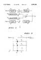
- FIG. 1is a block diagram illustrating a single cell of a field programmable analog array
- FIG. 2illustrates a simplified embodiment of an impedance block of FIG. 1
- FIG. 3is a schematic diagram illustrating the first compensation circuit of FIG. 1;
- FIG. 4illustrates an alternate embodiment of the first compensation circuit of FIG. 1
- FIG. 5is a schematic diagram illustrating the second compensation circuit of FIG. 1.
- a field programmable analog array cell 10is shown suitable for manufacturing as an integrated circuit using conventional integrated circuit processes.
- An analog input signal V IN1is applied to impedance block 12 that includes passive circuit elements such as capacitors serially and parallel coupled through a switching array to the inverting input of differential amplifier 14 at node 16.
- An analog input signal V IN2is applied to impedance block 18 that also includes a plurality of passive circuit elements such as capacitors coupled through a serial and parallel network of switches to the non-inverting input of amplifier 14 at node 20.
- An impedance block 22is coupled between the output of amplifier 14 and its inverting input.
- impedance block 24is coupled between the output of amplifier 14 and its non-inverting input. Impedance blocks 12, 18, 22, and 24 are programmed to close the appropriate switches to provide a predetermined function in response the input signals V IN1 and V IN2 to yield an analog signal V OUT .
- Field programmable analog array cell 10provides flexibility in design where the user may program the setting of switching circuits in the impedance blocks to achieve the appropriate impedance in the feed-forward and feed-back paths necessary to configure the amplifier according to the desired function.
- many array cellsare interconnected to form a complete analog array.
- the analog arraymay be fine-tuned, for example during test or field re-calibration, by changing the switch settings to adjust impedance values around the amplifier.
- impedance block 12including switching circuit 34 coupled between the input signal V IN1 and node 16.
- Capacitor 36 and switching circuit 38are serially coupled between the input signal V IN1 and node 16.
- Capacitor 40 and switching circuit 42are serially coupled between the input signal V IN1 and node 16, and capacitor 44 and switching circuit 46 are serially coupled between the input signal V IN1 and node 16.
- the embodiment shown in FIG. 2provides a simplified representation of the configuration of impedance block 12. It is understood that impedance block 12 typically contains many more switched capacitor elements, and other passive and/or active circuit elements, and a plurality of programmable switching circuits serially and parallel coupled to multiple input signals to provide flexibility in connecting a variety of cells to achieve the desired function.
- Impedance blocks 18, 22, and 24also include passive and/or active circuit elements interconnected by a plurality of programmable switching circuits as described for impedance block 12 to achieve the desired function.
- Switching circuit 34may comprise p-channel and n-channel CMOS transistors (not shown) with their drains coupled together for receiving input signal V IN1 and their sources coupled together to node 16. The gates of the p-channel and n-channel transistors receive complementary programming signals from a controller (not shown). Switching circuits 38, 42 and 46 are configured in a similar manner as described for switching circuit 34.
- the source diffusion area of the p-channel and n-channel transistors of switching circuits 34, 38, 42 and 46can source or sink a parasitic leakage current I L12 into or away from the inverting input of amplifier 14.
- a similar leakage current I L22 from impedance block 22flows into or away from the inverting input of amplifier 14.
- the inverting and non-inverting inputs of amplifier 14represent charge storage nodes within analog array cell 10 that are sensitive to charging and discharging by parasitic leakage currents.
- the large number of switches in impedance blocks 12, 18, 22, and 24'can create leakage currents of sufficient magnitude into the inverting and non-inverting inputs of amplifier 14 to cause an undesirable drift in the output voltage V OUT .
- compensation circuit 28is coupled to node 16 at the inverting input of amplifier 14 for sourcing or sinking a compensation current I 28 into or away from node 16 that is substantially equal to the summation of leakage currents I L12 and I L22 , say 10.0 nanoamps.
- the compensation current I 28has an opposite polarity with respect to the leakage current I L12 and I L22 so as to cancel their effect. That is, compensation circuit 28 draws a current away from node 16 equal to leakage currents flowing into the node such that no leakage current flows into the inverting input of amplifier 14 which in turn minimizes any drift in the output signal V OUT .
- compensation circuit 28may source a current into node 16 equal to leakage currents flowing away from that node such that a net zero current flows into node 16.
- compensation circuit 28includes transistor 50 having a gate coupled to power supply conductor 52 operating at a positive potential V DD such as 5.0 volts.
- the drain and source of transistor 50are coupled together for providing a source of leakage current.
- the source and drain diffusion area of transistor 50is sized to one-half the total diffusion areas of the p-channel transistors in the switches of impedance blocks 12 and 22.
- transistor 50is sized to 100.0 microns of width, i.e. 0.5 ⁇ 4 ⁇ 50.
- Compensation circuit 28further includes transistor 54 having a gate coupled to power supply conductor 56 operating at ground potential.
- the drain and source of transistor 54are coupled together for providing another source of leakage current.
- the source and drain diffusion areastill sink a leakagescurrent of say 12.0 nanoamps.
- Transistor 54is sized to have a source and drain diffusion area that is one-half the sum total of the diffusion areas of the n-channel transistors that comprise the switching circuits of impedance blocks 12 and 22.
- transistor 54is sized to 100.0 microns of width, i.e. 0.5 ⁇ 4 ⁇ 50.
- the sum of the diffusion areas of the p-channel transistors in the switching circuitsare equal to the diffusion area of p-channel transistor 50, while the sum of the diffusion areas of the n-channel transistors of the switching circuits equal to the diffusion area of n-channel transistor 54.
- the use of like semiconductor materialassures process and temperature independence for the leakage current compensation. Since only the source side of the n-channel and p-channel transistors of the switching circuits of impedance blocks 12 and 22 are coupled to node 16, transistors 50 and 54 are sized to one-half the total size of all the diffusion areas of the switching circuits that coupled to node 16.
- the common diffusion area of transistors 50 and 54is coupled to the cathode of diode 60 for providing a similar bias voltage as seen by the switching circuits in impedance blocks 12 and 22.
- the anode of diode 60is coupled to the drain and gate of transistor 62.
- the source of transistor 62is coupled to power supply conductor 52.
- the drain and gate of transistor 62is further coupled to the gate of transistor 64 for providing a current mirror operation to steer the leakage compensation current to node 16.
- the source of transistor 64is coupled to power supply conductor 52 while its drain is coupled to node 16.
- the current flowing through transistor 62 and diode 60is determined by the leakage currents of transistors 50 and 54.
- Transistor 50sources 2.0 nanoamps of leakage current while transistor 54 sinks 12.0 nanoamps of leakage current. That leaves 10.0 nanoamps flowing through diode 60 and transistor 62. That same leakage current is mirrored in transistor 64 and flows into node 16 as compensation current I 28 to cancel leakage currents I L12 and I L22 . At this current level, transistors 62 and 64 are operating in the weak inversion mode typical of battery operated devices such as digital watches. Diode 60 and transistors 62 and 64 also generate a small amount of parasitic leakage and must be taken into account in sizing transistors 50 and 54 to match the sum total of leakage currents from impedance blocks 12 and 22.
- the diffusion areas of transistors 50 and 54may be ratioed smaller to that of the sum total of diffusion areas of the switching circuits of impedance blocks 12 and 22. The smaller ratio may be necessary because of size restrictions on the integrated circuit die.
- the current mirror circuit 62-64is ratioed to provide the proper compensation current I 28 to cancel the leakage currents I L12 and I L22 . For example, if transistors 50 and 54 are reduced in size by a factor of five then transistor 64 is sized to have a width five times that of transistor 62.
- Transistor 66includes a drain and gate coupled together to the source and drain diffusion area of transistor 50, and a source coupled to power supply conductor 56.
- the gate of transistor 68is coupled to the gate and drain of transistor 66, while its source is coupled to power supply conductor 56.
- the drain of transistor 68is coupled to node 16.
- Transistor 50provides a leakage current of say 2.0 nanoamps into the current mirror arrangement 66-68.
- Transistor 54conducts 12.0 nanoamps of leakage current through diode 60 and transistor 62 which in turn is mirrored in transistor 64. With transistor 64 conducting 12.0 nanoamps and transistor 68 conducting 2.0 nanoamps of current, a net 10.0 nanoamps of compensation current I 28 flows into node 16 to cancel the leakage currents I L12 and I.sub. L22 from impedance blocks 12 and 22, respectively. Transistors 66 and 68 operate in the weak inversion mode for low current operation.
- compensation circuit 30provides an alternate approach to compensating for leakage. currents I L12 and I L22 by injecting a compensation current I 30 of the same polarity and magnitude as the sum of leakage currents I L12 and I L22 into node 20 at the non-inverting input of amplifier 14.
- the inverting input of amplifier 14receives the same amount of leakage current as the non-inverting input and therefore drift together as a common mode signal causing the output voltage V OUT to stay constant. That is, the identical leakage currents into the inverting and non-inverting inputs of amplifier 14 are rejected by the differential operation of amplifier 14. Compensation circuit 30 thus provides compensation of any leakage current into the inverting input of amplifier 14 to minimize drift in the output voltage V OUT .
- compensation circuit 30is shown with transistors 50 and 54 configured as described in FIG. 3.
- the common diffusion area of transistors 50 and 54is coupled to node 20.
- Capacitor 70is coupled between node 20 and power supply conductor 56. Capacitor 70 is selected at a value equal to the total capacitance between node 16 and the output of amplifier 14.
- a reference potential V REF operating at the midway point between power supply conductors 52 and 56 (2.5 volts)is coupled through switching circuit 72 to node 20.
- the internal switching circuitsoperate at predetermined phases of a clock signal to store and transfer charge from the input of the amplifier to its output.
- Switching circuit 72is closed at the beginning of the charge phase to charge node 20 to reference voltage V REF .
- Switching circuit 72opens at the beginning of the transfer phase whereby transistors 50 and 54 supply a leakage current that changes the voltage across capacitor 70 in the same manner as leakage currents I L12 and I L22 change the voltage at the inverting input of amplifier 14.
- the inverting and non-inverting inputs of amplifier 14receive the same change in voltage in a common mode manner that is canceled by the differential operation of amplifier 14.
- the leakage current cancellationremoves any drift of the output voltage V OUT attributed to leakage currents from impedance blocks 12 and 22.
- the present inventionprovides compensation of leakage current at the inputs of an amplifier, or any other charge storage node, in an analog array.
- Field programmable analog arraysprovide flexibility in design where the user may program the setting of switching circuits in the impedance blocks to effect the appropriate impedance in the feed-forward and feed-back paths to configure the amplifier according to the desired function.
- the large number of switches needed to program the impedance block and generate the proper responseinduce undesirable leakage currents.
- the compensation currentcancels the leakage currents to prevent drift in the output voltage of the analog array.
Landscapes
- Engineering & Computer Science (AREA)
- Power Engineering (AREA)
- Amplifiers (AREA)
Abstract
Description
The present invention relates in general to analog arrays and, more particularly, to leakage current compensation in the analog array.
Analog circuits are used in a variety of applications for providing functions such as filters, gains stages, analog-digital converters, etc. In the past, analog circuits have been generally designed for custom applications with a fixed amplifier stage and dedicated passive and/or active elements in the feed-forward and feed-back paths to perform the desired function. Each new circuit application typically requires a new design phase and layout phase which is a time consuming and expensive undertaking.
To bring products to market more efficiently, field programmable analog arrays have been developed to allow flexible implementations of analog functions. A typical field programmable analog array includes a fixed amplifier with programmable switched capacitor banks on its input terminals and feedback paths. The user need only program the switches to set the impedance values as needed to perform the analog function.
A common problem associated with switched impedance type field programmable arrays is the large number of switches needed to perform a useful function and the associated leakage current into the input terminals of the amplifier due to the large number of switches. The leakage current originates from the diffusion area of the switch contacts. Any leakage current introduced into the input terminals of the amplifier causes a voltage drift at the output of the amplifier. The diffusion current varies with process and increases with temperature thereby adding to the problem.
Hence, a need exists to minimize leakage current into the input terminals of the amplifier or any charge storage node associated with the field programmable analog array.
FIG. 1 is a block diagram illustrating a single cell of a field programmable analog array;
FIG. 2 illustrates a simplified embodiment of an impedance block of FIG. 1;
FIG. 3 is a schematic diagram illustrating the first compensation circuit of FIG. 1;
FIG. 4 illustrates an alternate embodiment of the first compensation circuit of FIG. 1; and
FIG. 5 is a schematic diagram illustrating the second compensation circuit of FIG. 1.
Referring to FIG. 1, a field programmableanalog array cell 10 is shown suitable for manufacturing as an integrated circuit using conventional integrated circuit processes. An analog input signal VIN1 is applied toimpedance block 12 that includes passive circuit elements such as capacitors serially and parallel coupled through a switching array to the inverting input ofdifferential amplifier 14 atnode 16. An analog input signal VIN2 is applied toimpedance block 18 that also includes a plurality of passive circuit elements such as capacitors coupled through a serial and parallel network of switches to the non-inverting input ofamplifier 14 atnode 20. Animpedance block 22 is coupled between the output ofamplifier 14 and its inverting input. Similarly,impedance block 24 is coupled between the output ofamplifier 14 and its non-inverting input.Impedance blocks
Field programmableanalog array cell 10 provides flexibility in design where the user may program the setting of switching circuits in the impedance blocks to achieve the appropriate impedance in the feed-forward and feed-back paths necessary to configure the amplifier according to the desired function. Typically, many array cells are interconnected to form a complete analog array. The analog array may be fine-tuned, for example during test or field re-calibration, by changing the switch settings to adjust impedance values around the amplifier.
Turning to FIG. 2, a simplified embodiment ofimpedance block 12 is shown includingswitching circuit 34 coupled between the input signal VIN1 andnode 16.Capacitor 36 andswitching circuit 38 are serially coupled between the input signal VIN1 andnode 16.Capacitor 40 andswitching circuit 42 are serially coupled between the input signal VIN1 andnode 16, andcapacitor 44 andswitching circuit 46 are serially coupled between the input signal VIN1 andnode 16. The embodiment shown in FIG. 2 provides a simplified representation of the configuration ofimpedance block 12. It is understood thatimpedance block 12 typically contains many more switched capacitor elements, and other passive and/or active circuit elements, and a plurality of programmable switching circuits serially and parallel coupled to multiple input signals to provide flexibility in connecting a variety of cells to achieve the desired function. Impedance blocks 18, 22, and 24 also include passive and/or active circuit elements interconnected by a plurality of programmable switching circuits as described forimpedance block 12 to achieve the desired function.
During normal operation, the source diffusion area of the p-channel and n-channel transistors of switchingcircuits amplifier 14. A similar leakage current IL22 fromimpedance block 22 flows into or away from the inverting input ofamplifier 14. The inverting and non-inverting inputs ofamplifier 14 represent charge storage nodes withinanalog array cell 10 that are sensitive to charging and discharging by parasitic leakage currents. The large number of switches in impedance blocks 12, 18, 22, and 24' can create leakage currents of sufficient magnitude into the inverting and non-inverting inputs ofamplifier 14 to cause an undesirable drift in the output voltage VOUT.
As part of the present invention,compensation circuit 28 is coupled tonode 16 at the inverting input ofamplifier 14 for sourcing or sinking a compensation current I28 into or away fromnode 16 that is substantially equal to the summation of leakage currents IL12 and IL22, say 10.0 nanoamps. The compensation current I28 has an opposite polarity with respect to the leakage current IL12 and IL22 so as to cancel their effect. That is,compensation circuit 28 draws a current away fromnode 16 equal to leakage currents flowing into the node such that no leakage current flows into the inverting input ofamplifier 14 which in turn minimizes any drift in the output signal VOUT. Alternately,compensation circuit 28 may source a current intonode 16 equal to leakage currents flowing away from that node such that a net zero current flows intonode 16.
Further detail ofcompensation circuit 28 is shown in FIG. 3 includingtransistor 50 having a gate coupled topower supply conductor 52 operating at a positive potential VDD such as 5.0 volts. The drain and source oftransistor 50 are coupled together for providing a source of leakage current. Although the high potential atpower supply conductor 52 keepstransistor 50 from operating in its normal mode, the source and drain diffusion area still cause a leakage current of say 2.0 nanoamps to flow. The source and drain diffusion area oftransistor 50 is sized to one-half the total diffusion areas of the p-channel transistors in the switches of impedance blocks 12 and 22. For example, if the source diffusion area of the p-channel transistors of switchingcircuits transistor 50 is sized to 100.0 microns of width, i.e. 0.5×4×50.
The sum of the diffusion areas of the p-channel transistors in the switching circuits are equal to the diffusion area of p-channel transistor 50, while the sum of the diffusion areas of the n-channel transistors of the switching circuits equal to the diffusion area of n-channel transistor 54. The use of like semiconductor material assures process and temperature independence for the leakage current compensation. Since only the source side of the n-channel and p-channel transistors of the switching circuits of impedance blocks 12 and 22 are coupled tonode 16,transistors node 16.
The common diffusion area oftransistors diode 60 for providing a similar bias voltage as seen by the switching circuits in impedance blocks 12 and 22. The anode ofdiode 60 is coupled to the drain and gate oftransistor 62. The source oftransistor 62 is coupled topower supply conductor 52. The drain and gate oftransistor 62 is further coupled to the gate oftransistor 64 for providing a current mirror operation to steer the leakage compensation current tonode 16. The source oftransistor 64 is coupled topower supply conductor 52 while its drain is coupled tonode 16. The current flowing throughtransistor 62 anddiode 60 is determined by the leakage currents oftransistors Transistor 50 sources 2.0 nanoamps of leakage current whiletransistor 54 sinks 12.0 nanoamps of leakage current. That leaves 10.0 nanoamps flowing throughdiode 60 andtransistor 62. That same leakage current is mirrored intransistor 64 and flows intonode 16 as compensation current I28 to cancel leakage currents IL12 and IL22. At this current level,transistors Diode 60 andtransistors transistors impedance blocks
In an alternate embodiment, the diffusion areas oftransistors transistors transistor 64 is sized to have a width five times that oftransistor 62.
Turning to FIG. 4, an alternate embodiment ofcompensation circuit 28 is shown. Components having a similar function are assigned the same reference numbers used in FIG. 3. An additional current mirrorcircuit comprising transistors Transistor 66 includes a drain and gate coupled together to the source and drain diffusion area oftransistor 50, and a source coupled topower supply conductor 56. The gate oftransistor 68 is coupled to the gate and drain oftransistor 66, while its source is coupled topower supply conductor 56. The drain oftransistor 68 is coupled tonode 16.Transistor 50 provides a leakage current of say 2.0 nanoamps into the current mirror arrangement 66-68.Transistor 54 conducts 12.0 nanoamps of leakage current throughdiode 60 andtransistor 62 which in turn is mirrored intransistor 64. Withtransistor 64 conducting 12.0 nanoamps andtransistor 68 conducting 2.0 nanoamps of current, a net 10.0 nanoamps of compensation current I28 flows intonode 16 to cancel the leakage currents IL12 and I.sub. L22 fromimpedance blocks Transistors
As another part of the present invention,compensation circuit 30 provides an alternate approach to compensating for leakage. currents IL12 and IL22 by injecting a compensation current I30 of the same polarity and magnitude as the sum of leakage currents IL12 and IL22 intonode 20 at the non-inverting input ofamplifier 14. The inverting input ofamplifier 14 receives the same amount of leakage current as the non-inverting input and therefore drift together as a common mode signal causing the output voltage VOUT to stay constant. That is, the identical leakage currents into the inverting and non-inverting inputs ofamplifier 14 are rejected by the differential operation ofamplifier 14.Compensation circuit 30 thus provides compensation of any leakage current into the inverting input ofamplifier 14 to minimize drift in the output voltage VOUT.
Referring now to FIG. 5,compensation circuit 30 is shown withtransistors transistors node 20.Capacitor 70 is coupled betweennode 20 andpower supply conductor 56.Capacitor 70 is selected at a value equal to the total capacitance betweennode 16 and the output ofamplifier 14. A reference potential VREF operating at the midway point betweenpower supply conductors 52 and 56 (2.5 volts) is coupled through switchingcircuit 72 tonode 20. In a switch capacitor arrangement of impedance blocks 12 and 22, the internal switching circuits operate at predetermined phases of a clock signal to store and transfer charge from the input of the amplifier to its output.Switching circuit 72 is closed at the beginning of the charge phase to chargenode 20 to reference voltage VREF. Switching circuit 72 opens at the beginning of the transfer phase wherebytransistors capacitor 70 in the same manner as leakage currents IL12 and IL22 change the voltage at the inverting input ofamplifier 14. Thus, the inverting and non-inverting inputs ofamplifier 14 receive the same change in voltage in a common mode manner that is canceled by the differential operation ofamplifier 14. The leakage current cancellation removes any drift of the output voltage VOUT attributed to leakage currents fromimpedance blocks
By now it should be appreciated that the present invention provides compensation of leakage current at the inputs of an amplifier, or any other charge storage node, in an analog array. Field programmable analog arrays provide flexibility in design where the user may program the setting of switching circuits in the impedance blocks to effect the appropriate impedance in the feed-forward and feed-back paths to configure the amplifier according to the desired function. The large number of switches needed to program the impedance block and generate the proper response induce undesirable leakage currents. The compensation current cancels the leakage currents to prevent drift in the output voltage of the analog array.
While specific embodiments of the present invention have been shown and described, further modifications and improvements will occur to those skilled in the art. It is understood that the invention is not limited to the particular forms shown and it is intended for the appended claims to cover all modifications which do not depart from the spirit and scope of this invention.
Claims (19)
1. An analog circuit, comprising:
an amplifier having first and second inputs and an output, said first input being coupled for receiving a first input signal, said output providing an output signal;
circuit means coupled between a terminal at which a second input signal is applied and said second input of said amplifier for providing a programmable impedance, said circuit means including a plurality of switches to control said programmable impedance; and
a compensation circuit coupled to said second input of said amplifier for providing a compensation current that cancels leakage current from said circuit means into said second input of said amplifier and prevents drift in said output signal of said amplifier.
2. The analog circuit of claim 1 wherein said compensation circuit includes:
a source of leakage current; and
current steering means having an input coupled to said source of leakage current and having an output for providing said compensation current to said second input of said amplifier.
3. The analog circuit of claim 2 wherein said source of leakage current includes a first transistor having a gate, a drain and a source, said gate being coupled to a first power supply conductor that renders said first transistor non-operational, said source being coupled to said drain for generating a first component of said compensation current, said first transistor having source and drain diffusion areas sized with respect to diffusion areas of like semiconductor material in said plurality of switches in said circuit means for providing said first component of said compensation current.
4. The analog circuit of claim 3 wherein said source of leakage current further includes a second transistor having a gate, a drain and a source, said gate being coupled to a second power supply conductor that Fenders said second transistor non-operational, said source being coupled to said drain for generating a second component of said compensation current, said second transistor having source and drain diffusion areas sized with respect to diffusion areas of like semiconductor material in said plurality of switches in said circuit means for providing said second component of said compensation current that in combination with said first component of said compensation current cancels said leakage current from said circuit means.
5. The analog circuit of claim 2 wherein said current steering means includes a current mirror circuit having an input coupled to said source of leakage current and having an output for providing said compensation current.
6. The analog circuit of claim 5 wherein said current mirror circuit includes:
a first transistor having a gate, a drain and a source, said source being coupled to a first power supply conductor, said gate and drain being coupled together to said source of leakage current; and
a second transistor having a gate, a drain and a source, said source being coupled to said first power supply conductor, said gate being coupled to said gate and drain of said first transistor, said drain providing said compensation current to said second input of said amplifier.
7. The analog circuit of claim 6 wherein said current steering means further includes a diode coupled between said source of leakage current and said drain of said first transistor.
8. The analog circuit of claim 1 wherein said compensation circuit includes:
a first source of leakage current;
a second source of leakage current; and
current steering means having first and second inputs coupled to said first and second sources of leakage current respectively and having an output for providing said compensation current.
9. The analog circuit of claim 8 wherein said first source of leakage current includes a first transistor having a gate, a drain and a source, said gate being coupled to a first power supply conductor that renders said first transistor non-operational, said source being coupled to said drain for generating a first component of said compensation current, said first transistor having source and drain diffusion areas sized with respect to diffusion areas of like semiconductor material in said plurality of switches in said circuit means for providing said first component of said compensation current.
10. The analog-circuit of claim 9 wherein said second source of leakage current includes a second transistor having a gate, a drain and a source, said gate being coupled to a second power supply conductor that renders said second transistor non-operational, said source being coupled to said drain for generating a second component of said compensation current, said second transistor having source and drain diffusion areas sized with respect to diffusion areas of like semiconductor material in said plurality of switches in said circuit means for providing said second component of said compensation current that in combination with said first component of said compensation current cancels said leakage current from said circuit means.
11. The analog circuit of claim 10 wherein said current steering means includes:
a first current mirror circuit having an input coupled to said first source of leakage current and having an output coupled to said second input of said amplifier; and
a second current mirror circuit having an input coupled to said second source of leakage current and having an output coupled to said second input of said amplifier for providing said compensation current.
12. The analog circuit of claim 11 wherein said first current mirror circuit includes:
a first transistor having a gate, a drain and a source, said source being coupled to said first power supply conductor, said gate and drain being coupled together to said first source of leakage current; and
a second transistor having a gate, a drain and a source, said source being coupled to said first power supply conductor, said gate being coupled to said gate and drain of said first transistor, said drain providing said first component of said compensation current to said second input of said amplifier.
13. The analog circuit of claim 12 wherein said second current mirror circuit includes:
a third transistor having a gate, a drain and a source, said source being coupled to said second power supply conductor, said gate and drain being coupled together to said second source of leakage current; and
a fourth transistor having a gate, a drain and a source, said source being coupled to said second power supply conductor, said gate being coupled to said gate and drain of said third transistor, said drain providing said second component of said compensation current to said second input of said amplifier.
14. An analog circuit, comprising:
an amplifier having first and second inputs and an output, said first input being coupled for receiving a first input signal, said output providing an output signal;
circuit means coupled between a terminal at which a second input signal is applied and said second input of said amplifier for providing a programmable impedance, said circuit means including a plurality of switches to control said programmable impedance; and
a compensation circuit coupled to said first input of said amplifier for providing a compensation current that matches leakage current from said circuit means into said second input of said amplifier and prevents drift in said output signal of said amplifier.
15. The analog circuit of claim 14 wherein said compensation circuit includes:
a source of leakage current;
a capacitor coupled between said first input of said amplifier and a first power supply conductor; and
a switching circuit coupled between a terminal at which a reference voltage is applied and said first input of said amplifier.
16. The analog circuit of claim 15 wherein said capacitor is sized to match total capacitance that connects between said output of said amplifier and said first input of said amplifier.
17. The analog circuit of claim 16 wherein said source of leakage current includes a first transistor having a gate, a drain and a source, said gate being coupled to a first power supply conductor that renders said first transistor non-operational, said source being coupled to said drain for generating a first component of said compensation current, said first transistor having source and drain diffusion areas sized with respect to diffusion areas of like semiconductor material in said plurality of switches in said circuit means for providing said first component of said compensation current.
18. The analog circuit of claim 17 wherein said source of leakage current further includes a second transistor having a gate, a drain and a source, said gate being coupled to a second power supply conductor that fenders said second transistor non-operational, said source being coupled to said drain for generating a second component of said compensation current, said second transistor having source and drain diffusion areas sized with respect to diffusion areas of like semiconductor material in said plurality of switches in said circuit means for providing said second component of said compensation current that in combination with said first component of said compensation current cancels said leakage current from said circuit means.
19. A method of compensating for leakage current in an analog circuit, comprising the steps of:
providing a differential amplifier having first and second inputs;
providing a parasitic leakage current into said first input of said differential amplifier; and
injecting a compensation current into said second input of said differential amplifier that matches said parasitic leakage current and cancels effects of said parasitic leakage current by creating a common mode signal that is rejected by said differential amplifier.
Priority Applications (4)
| Application Number | Priority Date | Filing Date | Title |
|---|---|---|---|
| US08/300,906US5493246A (en) | 1994-09-06 | 1994-09-06 | Circuit and method of canceling leakage current in an analog array |
| DE69519837TDE69519837T2 (en) | 1994-09-06 | 1995-08-31 | Circuit and method for leakage current compensation in an analog arrangement |
| EP95113676AEP0701321B1 (en) | 1994-09-06 | 1995-08-31 | Circuit and method of cancelling leakage current in an analog array |
| JP7246996AJPH0888520A (en) | 1994-09-06 | 1995-09-01 | Circuit and method for cahceling leakage current in analog array |
Applications Claiming Priority (1)
| Application Number | Priority Date | Filing Date | Title |
|---|---|---|---|
| US08/300,906US5493246A (en) | 1994-09-06 | 1994-09-06 | Circuit and method of canceling leakage current in an analog array |
Publications (1)
| Publication Number | Publication Date |
|---|---|
| US5493246Atrue US5493246A (en) | 1996-02-20 |
Family
ID=23161101
Family Applications (1)
| Application Number | Title | Priority Date | Filing Date |
|---|---|---|---|
| US08/300,906Expired - Fee RelatedUS5493246A (en) | 1994-09-06 | 1994-09-06 | Circuit and method of canceling leakage current in an analog array |
Country Status (4)
| Country | Link |
|---|---|
| US (1) | US5493246A (en) |
| EP (1) | EP0701321B1 (en) |
| JP (1) | JPH0888520A (en) |
| DE (1) | DE69519837T2 (en) |
Cited By (76)
| Publication number | Priority date | Publication date | Assignee | Title |
|---|---|---|---|---|
| US5680070A (en)* | 1996-02-05 | 1997-10-21 | Motorola, Inc. | Programmable analog array and method for configuring the same |
| US5821795A (en)* | 1997-02-11 | 1998-10-13 | International Business Machines Corporation | Circuit for cancelling the DC offset in a differential analog front end of a read channel |
| WO1998049565A1 (en)* | 1997-04-30 | 1998-11-05 | Credence Systems Corporation | Integrated circuit tester with compensation for leakage current |
| US5892375A (en)* | 1997-08-26 | 1999-04-06 | Harris Corporation | Comparator with small signal suppression circuitry |
| US5936469A (en)* | 1997-08-04 | 1999-08-10 | Motorola, Inc. | Amplifier with input referred common-mode adjustment |
| US6229845B1 (en) | 1999-02-25 | 2001-05-08 | Qlogic Corporation | Bus driver with data dependent drive strength control logic |
| WO2002058070A3 (en)* | 2001-01-19 | 2002-11-07 | Infineon Technologies Ag | Selection device for a semiconductor memory device |
| US20020186245A1 (en)* | 2000-06-13 | 2002-12-12 | Sundeep Chandhoke | System and method for configuring a hardware device to execute a prototype |
| US20030048830A1 (en)* | 2001-09-12 | 2003-03-13 | Alstom Power N.V. | Apparatus for evaluating data representing the electrical characteristics of a combustion vessel |
| US6541996B1 (en)* | 1999-12-21 | 2003-04-01 | Ati International Srl | Dynamic impedance compensation circuit and method |
| US20030076945A1 (en)* | 2001-10-24 | 2003-04-24 | George Huang | Automatic longitudinal balance for solid state DAAs |
| WO2003094172A1 (en)* | 2002-04-30 | 2003-11-13 | Infineon Technologies Ag | Integrated circuit with a sample-and-hold device |
| US6667650B2 (en)* | 2002-03-27 | 2003-12-23 | Texas Instruments Incorporated | Current leakage compensation circuit and method |
| US20040174240A1 (en)* | 2002-12-11 | 2004-09-09 | Canon Kabushiki Kaisha | Electrical device and method of producing the same |
| US20040201419A1 (en)* | 2003-04-14 | 2004-10-14 | Chao-Cheng Lee | Amplifying circuit |
| US20050068095A1 (en)* | 2003-09-08 | 2005-03-31 | Chia-Jun Chang | Low pass filter |
| US20050151576A1 (en)* | 2003-09-23 | 2005-07-14 | Chao-Cheng Lee | Adjustable impedance circuit |
| US6941336B1 (en)* | 2000-10-26 | 2005-09-06 | Cypress Semiconductor Corporation | Programmable analog system architecture |
| US7092980B1 (en)* | 2000-10-26 | 2006-08-15 | Cypress Semiconductor Corporation | Programming architecture for a programmable analog system |
| US20060294523A1 (en)* | 2005-06-23 | 2006-12-28 | Paul Beard | Touch wake for electronic devices |
| US7376205B1 (en)* | 2001-11-20 | 2008-05-20 | Xilinx, Inc. | Device and method for compensation of transmission line distortion |
| US20080136492A1 (en)* | 2006-12-06 | 2008-06-12 | Texas Instruments Incorporated | Leakage compensation circuit using limiting current inverter |
| US20080258760A1 (en)* | 2007-04-17 | 2008-10-23 | Cypress Semiconductor Corporation | System level interconnect with programmable switching |
| US20080258804A1 (en)* | 2007-04-17 | 2008-10-23 | Cypress Semiconductor Corporation | Numerical band gap |
| US20080288755A1 (en)* | 2007-04-17 | 2008-11-20 | Cypress Semiconductor Corporation | Clock driven dynamic datapath chaining |
| US20080301619A1 (en)* | 2001-11-19 | 2008-12-04 | Cypress Semiconductor Corporation | System and method for performing next placements and pruning of disallowed placements for programming an integrated circuit |
| US7737724B2 (en) | 2007-04-17 | 2010-06-15 | Cypress Semiconductor Corporation | Universal digital block interconnection and channel routing |
| US7761845B1 (en) | 2002-09-09 | 2010-07-20 | Cypress Semiconductor Corporation | Method for parameterizing a user module |
| US7765095B1 (en) | 2000-10-26 | 2010-07-27 | Cypress Semiconductor Corporation | Conditional branching in an in-circuit emulation system |
| US7770113B1 (en) | 2001-11-19 | 2010-08-03 | Cypress Semiconductor Corporation | System and method for dynamically generating a configuration datasheet |
| US7774190B1 (en) | 2001-11-19 | 2010-08-10 | Cypress Semiconductor Corporation | Sleep and stall in an in-circuit emulation system |
| US7825688B1 (en) | 2000-10-26 | 2010-11-02 | Cypress Semiconductor Corporation | Programmable microcontroller architecture(mixed analog/digital) |
| US7893724B2 (en) | 2004-03-25 | 2011-02-22 | Cypress Semiconductor Corporation | Method and circuit for rapid alignment of signals |
| US8040266B2 (en) | 2007-04-17 | 2011-10-18 | Cypress Semiconductor Corporation | Programmable sigma-delta analog-to-digital converter |
| US8049569B1 (en) | 2007-09-05 | 2011-11-01 | Cypress Semiconductor Corporation | Circuit and method for improving the accuracy of a crystal-less oscillator having dual-frequency modes |
| US8069428B1 (en) | 2001-10-24 | 2011-11-29 | Cypress Semiconductor Corporation | Techniques for generating microcontroller configuration information |
| US8069405B1 (en) | 2001-11-19 | 2011-11-29 | Cypress Semiconductor Corporation | User interface for efficiently browsing an electronic document using data-driven tabs |
| US8067948B2 (en) | 2006-03-27 | 2011-11-29 | Cypress Semiconductor Corporation | Input/output multiplexer bus |
| US8069436B2 (en) | 2004-08-13 | 2011-11-29 | Cypress Semiconductor Corporation | Providing hardware independence to automate code generation of processing device firmware |
| US8078970B1 (en) | 2001-11-09 | 2011-12-13 | Cypress Semiconductor Corporation | Graphical user interface with user-selectable list-box |
| US8078894B1 (en) | 2007-04-25 | 2011-12-13 | Cypress Semiconductor Corporation | Power management architecture, method and configuration system |
| US8085067B1 (en) | 2005-12-21 | 2011-12-27 | Cypress Semiconductor Corporation | Differential-to-single ended signal converter circuit and method |
| US8085100B2 (en) | 2005-02-04 | 2011-12-27 | Cypress Semiconductor Corporation | Poly-phase frequency synthesis oscillator |
| US8092083B2 (en) | 2007-04-17 | 2012-01-10 | Cypress Semiconductor Corporation | Temperature sensor with digital bandgap |
| US8103496B1 (en) | 2000-10-26 | 2012-01-24 | Cypress Semicondutor Corporation | Breakpoint control in an in-circuit emulation system |
| US8103497B1 (en) | 2002-03-28 | 2012-01-24 | Cypress Semiconductor Corporation | External interface for event architecture |
| US8120408B1 (en) | 2005-05-05 | 2012-02-21 | Cypress Semiconductor Corporation | Voltage controlled oscillator delay cell and method |
| US8149048B1 (en) | 2000-10-26 | 2012-04-03 | Cypress Semiconductor Corporation | Apparatus and method for programmable power management in a programmable analog circuit block |
| US8160864B1 (en) | 2000-10-26 | 2012-04-17 | Cypress Semiconductor Corporation | In-circuit emulator and pod synchronized boot |
| US8176296B2 (en) | 2000-10-26 | 2012-05-08 | Cypress Semiconductor Corporation | Programmable microcontroller architecture |
| US8286125B2 (en) | 2004-08-13 | 2012-10-09 | Cypress Semiconductor Corporation | Model for a hardware device-independent method of defining embedded firmware for programmable systems |
| US8402313B1 (en) | 2002-05-01 | 2013-03-19 | Cypress Semiconductor Corporation | Reconfigurable testing system and method |
| US8499270B1 (en) | 2007-04-25 | 2013-07-30 | Cypress Semiconductor Corporation | Configuration of programmable IC design elements |
| US8533677B1 (en) | 2001-11-19 | 2013-09-10 | Cypress Semiconductor Corporation | Graphical user interface for dynamically reconfiguring a programmable device |
| US20140376419A1 (en)* | 2012-12-11 | 2014-12-25 | University Of Southern California | Passive leakage cancellation networks for duplexers and coexisting wireless communication systems |
| WO2014209662A1 (en)* | 2013-06-28 | 2014-12-31 | Qualcomm Incorporated | Circuits for semiconductor device leakage cancellation |
| US9448964B2 (en) | 2009-05-04 | 2016-09-20 | Cypress Semiconductor Corporation | Autonomous control in a programmable system |
| US9564902B2 (en) | 2007-04-17 | 2017-02-07 | Cypress Semiconductor Corporation | Dynamically configurable and re-configurable data path |
| US9590794B2 (en) | 2013-12-10 | 2017-03-07 | University Of Southern California | Enhancing isolation and impedance matching in hybrid-based cancellation networks and duplexers |
| CN107005216A (en)* | 2014-12-03 | 2017-08-01 | 瑞典爱立信有限公司 | Attenuator |
| US9720805B1 (en) | 2007-04-25 | 2017-08-01 | Cypress Semiconductor Corporation | System and method for controlling a target device |
| US9755668B2 (en) | 2015-09-30 | 2017-09-05 | Abtum Inc. | Radio frequency complex reflection coefficient reader |
| US9762416B2 (en) | 2015-09-08 | 2017-09-12 | Abtum Inc. | Reflection coefficient reader |
| US9843302B2 (en) | 2014-02-14 | 2017-12-12 | University Of Southern California | Reflection and hybrid reflection filters |
| US9866201B2 (en) | 2015-09-08 | 2018-01-09 | Abtum Inc. | All-acoustic duplexers using directional couplers |
| US9871543B2 (en) | 2014-02-19 | 2018-01-16 | University Of Southern California | Miniature acoustic resonator-based filters and duplexers with cancellation methodology |
| US9912326B2 (en) | 2015-09-08 | 2018-03-06 | Abtum Inc. | Method for tuning feed-forward canceller |
| US10038458B2 (en) | 2015-10-06 | 2018-07-31 | Abtum Inc. | Reflection-based radio-frequency multiplexers |
| US10476530B2 (en) | 2015-10-12 | 2019-11-12 | Qorvo Us, Inc. | Hybrid-coupler-based radio frequency multiplexers |
| US10581650B2 (en) | 2015-09-08 | 2020-03-03 | Qorvo Us, Inc. | Enhancing isolation in radio frequency multiplexers |
| US10615949B2 (en) | 2014-02-14 | 2020-04-07 | University Of Southern California | Hybrid-based cancellation in presence of antenna mismatch |
| US10698662B2 (en) | 2001-11-15 | 2020-06-30 | Cypress Semiconductor Corporation | System providing automatic source code generation for personalization and parameterization of user modules |
| US10855246B2 (en) | 2016-09-21 | 2020-12-01 | Qorvo Us, Inc. | Enhancing isolation in hybrid-based radio frequency duplexers and multiplexers |
| JP2022045890A (en)* | 2020-09-09 | 2022-03-22 | エスケーハイニックス株式会社 | Analog-to-digital conversion circuit and image sensor |
| WO2022205764A1 (en)* | 2021-03-29 | 2022-10-06 | 普源精电科技股份有限公司 | Switch circuit, chip, and signal processing device |
| US11499995B2 (en) | 2020-10-26 | 2022-11-15 | Analog Devices, Inc. | Leakage compensation technique for current sensor |
Families Citing this family (1)
| Publication number | Priority date | Publication date | Assignee | Title |
|---|---|---|---|---|
| JP6114208B2 (en)* | 2014-02-06 | 2017-04-12 | 日本電信電話株式会社 | Leakage current elimination circuit |
Citations (5)
| Publication number | Priority date | Publication date | Assignee | Title |
|---|---|---|---|---|
| US4163947A (en)* | 1977-09-23 | 1979-08-07 | Analogic Corporation | Current and voltage autozeroing integrator |
| US4216394A (en)* | 1978-06-26 | 1980-08-05 | Rca Corporation | Leakage current compensation circuit |
| US4555668A (en)* | 1983-10-14 | 1985-11-26 | American Microsystems, Inc. | Gain amplifier |
| US4885548A (en)* | 1987-07-24 | 1989-12-05 | Nippon Telegraph And Telephone Corporation | Wideband amplifier |
| US4988900A (en)* | 1988-12-28 | 1991-01-29 | Sgs-Thomson Microelectronics S.A. | Analog signal waveform generator |
Family Cites Families (4)
| Publication number | Priority date | Publication date | Assignee | Title |
|---|---|---|---|---|
| US3725804A (en)* | 1971-11-26 | 1973-04-03 | Avco Corp | Capacitance compensation circuit for differential amplifier |
| US4417160A (en)* | 1981-07-30 | 1983-11-22 | Rca Corporation | Offset compensation apparatus for biasing an analog comparator |
| US4565971A (en)* | 1985-01-28 | 1986-01-21 | Motorola, Inc. | Parasitic insensitive auto-zeroed operational amplifier |
| US4713625A (en)* | 1986-12-15 | 1987-12-15 | Motorola, Inc. | Circuit for improving power supply rejection in an operational amplifier with frequency compensation |
- 1994
- 1994-09-06USUS08/300,906patent/US5493246A/ennot_activeExpired - Fee Related
- 1995
- 1995-08-31EPEP95113676Apatent/EP0701321B1/ennot_activeExpired - Lifetime
- 1995-08-31DEDE69519837Tpatent/DE69519837T2/ennot_activeExpired - Fee Related
- 1995-09-01JPJP7246996Apatent/JPH0888520A/enactivePending
Patent Citations (5)
| Publication number | Priority date | Publication date | Assignee | Title |
|---|---|---|---|---|
| US4163947A (en)* | 1977-09-23 | 1979-08-07 | Analogic Corporation | Current and voltage autozeroing integrator |
| US4216394A (en)* | 1978-06-26 | 1980-08-05 | Rca Corporation | Leakage current compensation circuit |
| US4555668A (en)* | 1983-10-14 | 1985-11-26 | American Microsystems, Inc. | Gain amplifier |
| US4885548A (en)* | 1987-07-24 | 1989-12-05 | Nippon Telegraph And Telephone Corporation | Wideband amplifier |
| US4988900A (en)* | 1988-12-28 | 1991-01-29 | Sgs-Thomson Microelectronics S.A. | Analog signal waveform generator |
Cited By (113)
| Publication number | Priority date | Publication date | Assignee | Title |
|---|---|---|---|---|
| US5680070A (en)* | 1996-02-05 | 1997-10-21 | Motorola, Inc. | Programmable analog array and method for configuring the same |
| US5821795A (en)* | 1997-02-11 | 1998-10-13 | International Business Machines Corporation | Circuit for cancelling the DC offset in a differential analog front end of a read channel |
| WO1998049565A1 (en)* | 1997-04-30 | 1998-11-05 | Credence Systems Corporation | Integrated circuit tester with compensation for leakage current |
| US5999008A (en)* | 1997-04-30 | 1999-12-07 | Credence Systems Corporation | Integrated circuit tester with compensation for leakage current |
| US5936469A (en)* | 1997-08-04 | 1999-08-10 | Motorola, Inc. | Amplifier with input referred common-mode adjustment |
| US5892375A (en)* | 1997-08-26 | 1999-04-06 | Harris Corporation | Comparator with small signal suppression circuitry |
| US6229845B1 (en) | 1999-02-25 | 2001-05-08 | Qlogic Corporation | Bus driver with data dependent drive strength control logic |
| US6541996B1 (en)* | 1999-12-21 | 2003-04-01 | Ati International Srl | Dynamic impedance compensation circuit and method |
| US20020186245A1 (en)* | 2000-06-13 | 2002-12-12 | Sundeep Chandhoke | System and method for configuring a hardware device to execute a prototype |
| US8640027B2 (en) | 2000-06-13 | 2014-01-28 | National Instruments Corporation | System and method for configuring a hardware device to execute a prototype |
| US8555032B2 (en) | 2000-10-26 | 2013-10-08 | Cypress Semiconductor Corporation | Microcontroller programmable system on a chip with programmable interconnect |
| US8736303B2 (en) | 2000-10-26 | 2014-05-27 | Cypress Semiconductor Corporation | PSOC architecture |
| US8176296B2 (en) | 2000-10-26 | 2012-05-08 | Cypress Semiconductor Corporation | Programmable microcontroller architecture |
| US8160864B1 (en) | 2000-10-26 | 2012-04-17 | Cypress Semiconductor Corporation | In-circuit emulator and pod synchronized boot |
| US7765095B1 (en) | 2000-10-26 | 2010-07-27 | Cypress Semiconductor Corporation | Conditional branching in an in-circuit emulation system |
| US9843327B1 (en) | 2000-10-26 | 2017-12-12 | Cypress Semiconductor Corporation | PSOC architecture |
| US8149048B1 (en) | 2000-10-26 | 2012-04-03 | Cypress Semiconductor Corporation | Apparatus and method for programmable power management in a programmable analog circuit block |
| US8103496B1 (en) | 2000-10-26 | 2012-01-24 | Cypress Semicondutor Corporation | Breakpoint control in an in-circuit emulation system |
| US7825688B1 (en) | 2000-10-26 | 2010-11-02 | Cypress Semiconductor Corporation | Programmable microcontroller architecture(mixed analog/digital) |
| US10020810B2 (en) | 2000-10-26 | 2018-07-10 | Cypress Semiconductor Corporation | PSoC architecture |
| US10248604B2 (en) | 2000-10-26 | 2019-04-02 | Cypress Semiconductor Corporation | Microcontroller programmable system on a chip |
| US9766650B2 (en) | 2000-10-26 | 2017-09-19 | Cypress Semiconductor Corporation | Microcontroller programmable system on a chip with programmable interconnect |
| US6941336B1 (en)* | 2000-10-26 | 2005-09-06 | Cypress Semiconductor Corporation | Programmable analog system architecture |
| US10261932B2 (en) | 2000-10-26 | 2019-04-16 | Cypress Semiconductor Corporation | Microcontroller programmable system on a chip |
| US8358150B1 (en) | 2000-10-26 | 2013-01-22 | Cypress Semiconductor Corporation | Programmable microcontroller architecture(mixed analog/digital) |
| US7092980B1 (en)* | 2000-10-26 | 2006-08-15 | Cypress Semiconductor Corporation | Programming architecture for a programmable analog system |
| US10725954B2 (en) | 2000-10-26 | 2020-07-28 | Monterey Research, Llc | Microcontroller programmable system on a chip |
| WO2002058070A3 (en)* | 2001-01-19 | 2002-11-07 | Infineon Technologies Ag | Selection device for a semiconductor memory device |
| US6888744B2 (en) | 2001-01-19 | 2005-05-03 | Infineon Technologies Ag | Selection device for a semiconductor memory device |
| US20040141388A1 (en)* | 2001-01-19 | 2004-07-22 | Hans-Heinrich Viehmann | Selection device for a semiconductor memory device |
| US20030048830A1 (en)* | 2001-09-12 | 2003-03-13 | Alstom Power N.V. | Apparatus for evaluating data representing the electrical characteristics of a combustion vessel |
| US6750660B2 (en)* | 2001-09-12 | 2004-06-15 | Alstom Technology Ltd | Apparatus for evaluating data representing the electrical characteristics of a combustion vessel |
| US8793635B1 (en) | 2001-10-24 | 2014-07-29 | Cypress Semiconductor Corporation | Techniques for generating microcontroller configuration information |
| US8069428B1 (en) | 2001-10-24 | 2011-11-29 | Cypress Semiconductor Corporation | Techniques for generating microcontroller configuration information |
| US10466980B2 (en) | 2001-10-24 | 2019-11-05 | Cypress Semiconductor Corporation | Techniques for generating microcontroller configuration information |
| US20030076945A1 (en)* | 2001-10-24 | 2003-04-24 | George Huang | Automatic longitudinal balance for solid state DAAs |
| US8078970B1 (en) | 2001-11-09 | 2011-12-13 | Cypress Semiconductor Corporation | Graphical user interface with user-selectable list-box |
| US10698662B2 (en) | 2001-11-15 | 2020-06-30 | Cypress Semiconductor Corporation | System providing automatic source code generation for personalization and parameterization of user modules |
| US8069405B1 (en) | 2001-11-19 | 2011-11-29 | Cypress Semiconductor Corporation | User interface for efficiently browsing an electronic document using data-driven tabs |
| US8533677B1 (en) | 2001-11-19 | 2013-09-10 | Cypress Semiconductor Corporation | Graphical user interface for dynamically reconfiguring a programmable device |
| US7770113B1 (en) | 2001-11-19 | 2010-08-03 | Cypress Semiconductor Corporation | System and method for dynamically generating a configuration datasheet |
| US7844437B1 (en) | 2001-11-19 | 2010-11-30 | Cypress Semiconductor Corporation | System and method for performing next placements and pruning of disallowed placements for programming an integrated circuit |
| US8370791B2 (en) | 2001-11-19 | 2013-02-05 | Cypress Semiconductor Corporation | System and method for performing next placements and pruning of disallowed placements for programming an integrated circuit |
| US20080301619A1 (en)* | 2001-11-19 | 2008-12-04 | Cypress Semiconductor Corporation | System and method for performing next placements and pruning of disallowed placements for programming an integrated circuit |
| US7774190B1 (en) | 2001-11-19 | 2010-08-10 | Cypress Semiconductor Corporation | Sleep and stall in an in-circuit emulation system |
| US7376205B1 (en)* | 2001-11-20 | 2008-05-20 | Xilinx, Inc. | Device and method for compensation of transmission line distortion |
| US6667650B2 (en)* | 2002-03-27 | 2003-12-23 | Texas Instruments Incorporated | Current leakage compensation circuit and method |
| US8103497B1 (en) | 2002-03-28 | 2012-01-24 | Cypress Semiconductor Corporation | External interface for event architecture |
| WO2003094172A1 (en)* | 2002-04-30 | 2003-11-13 | Infineon Technologies Ag | Integrated circuit with a sample-and-hold device |
| US6965258B2 (en) | 2002-04-30 | 2005-11-15 | Infineon Technologies Ag | Sample-and-hold with no-delay reset |
| US20040239378A1 (en)* | 2002-04-30 | 2004-12-02 | Peter Bogner | Sample-and-hold with no-delay reset |
| US8402313B1 (en) | 2002-05-01 | 2013-03-19 | Cypress Semiconductor Corporation | Reconfigurable testing system and method |
| US7761845B1 (en) | 2002-09-09 | 2010-07-20 | Cypress Semiconductor Corporation | Method for parameterizing a user module |
| US20040174240A1 (en)* | 2002-12-11 | 2004-09-09 | Canon Kabushiki Kaisha | Electrical device and method of producing the same |
| US20040201419A1 (en)* | 2003-04-14 | 2004-10-14 | Chao-Cheng Lee | Amplifying circuit |
| US7106131B2 (en)* | 2003-04-14 | 2006-09-12 | Realtek Semiconductor Corp. | Amplifying circuit |
| US7023263B2 (en) | 2003-09-08 | 2006-04-04 | Realtek Semiconductor Corp. | Low pass filter |
| US20050068095A1 (en)* | 2003-09-08 | 2005-03-31 | Chia-Jun Chang | Low pass filter |
| US20050151576A1 (en)* | 2003-09-23 | 2005-07-14 | Chao-Cheng Lee | Adjustable impedance circuit |
| US7893724B2 (en) | 2004-03-25 | 2011-02-22 | Cypress Semiconductor Corporation | Method and circuit for rapid alignment of signals |
| US8069436B2 (en) | 2004-08-13 | 2011-11-29 | Cypress Semiconductor Corporation | Providing hardware independence to automate code generation of processing device firmware |
| US8286125B2 (en) | 2004-08-13 | 2012-10-09 | Cypress Semiconductor Corporation | Model for a hardware device-independent method of defining embedded firmware for programmable systems |
| US8085100B2 (en) | 2005-02-04 | 2011-12-27 | Cypress Semiconductor Corporation | Poly-phase frequency synthesis oscillator |
| US8120408B1 (en) | 2005-05-05 | 2012-02-21 | Cypress Semiconductor Corporation | Voltage controlled oscillator delay cell and method |
| US20060294523A1 (en)* | 2005-06-23 | 2006-12-28 | Paul Beard | Touch wake for electronic devices |
| US8089461B2 (en) | 2005-06-23 | 2012-01-03 | Cypress Semiconductor Corporation | Touch wake for electronic devices |
| US8085067B1 (en) | 2005-12-21 | 2011-12-27 | Cypress Semiconductor Corporation | Differential-to-single ended signal converter circuit and method |
| US8067948B2 (en) | 2006-03-27 | 2011-11-29 | Cypress Semiconductor Corporation | Input/output multiplexer bus |
| US8717042B1 (en) | 2006-03-27 | 2014-05-06 | Cypress Semiconductor Corporation | Input/output multiplexer bus |
| US20080136492A1 (en)* | 2006-12-06 | 2008-06-12 | Texas Instruments Incorporated | Leakage compensation circuit using limiting current inverter |
| US7642814B2 (en)* | 2006-12-06 | 2010-01-05 | Texas Instruments Incorporated | Leakage compensation circuit using limiting current inverter |
| US20080288755A1 (en)* | 2007-04-17 | 2008-11-20 | Cypress Semiconductor Corporation | Clock driven dynamic datapath chaining |
| US9564902B2 (en) | 2007-04-17 | 2017-02-07 | Cypress Semiconductor Corporation | Dynamically configurable and re-configurable data path |
| US8476928B1 (en) | 2007-04-17 | 2013-07-02 | Cypress Semiconductor Corporation | System level interconnect with programmable switching |
| US8092083B2 (en) | 2007-04-17 | 2012-01-10 | Cypress Semiconductor Corporation | Temperature sensor with digital bandgap |
| US8516025B2 (en) | 2007-04-17 | 2013-08-20 | Cypress Semiconductor Corporation | Clock driven dynamic datapath chaining |
| US20080258760A1 (en)* | 2007-04-17 | 2008-10-23 | Cypress Semiconductor Corporation | System level interconnect with programmable switching |
| US7737724B2 (en) | 2007-04-17 | 2010-06-15 | Cypress Semiconductor Corporation | Universal digital block interconnection and channel routing |
| US8130025B2 (en) | 2007-04-17 | 2012-03-06 | Cypress Semiconductor Corporation | Numerical band gap |
| US8040266B2 (en) | 2007-04-17 | 2011-10-18 | Cypress Semiconductor Corporation | Programmable sigma-delta analog-to-digital converter |
| US8026739B2 (en) | 2007-04-17 | 2011-09-27 | Cypress Semiconductor Corporation | System level interconnect with programmable switching |
| US20080258804A1 (en)* | 2007-04-17 | 2008-10-23 | Cypress Semiconductor Corporation | Numerical band gap |
| US8499270B1 (en) | 2007-04-25 | 2013-07-30 | Cypress Semiconductor Corporation | Configuration of programmable IC design elements |
| US8078894B1 (en) | 2007-04-25 | 2011-12-13 | Cypress Semiconductor Corporation | Power management architecture, method and configuration system |
| US9720805B1 (en) | 2007-04-25 | 2017-08-01 | Cypress Semiconductor Corporation | System and method for controlling a target device |
| US8909960B1 (en) | 2007-04-25 | 2014-12-09 | Cypress Semiconductor Corporation | Power management architecture, method and configuration system |
| US8049569B1 (en) | 2007-09-05 | 2011-11-01 | Cypress Semiconductor Corporation | Circuit and method for improving the accuracy of a crystal-less oscillator having dual-frequency modes |
| US9448964B2 (en) | 2009-05-04 | 2016-09-20 | Cypress Semiconductor Corporation | Autonomous control in a programmable system |
| US9490866B2 (en)* | 2012-12-11 | 2016-11-08 | University Of Southern California | Passive leakage cancellation networks for duplexers and coexisting wireless communication systems |
| US20140376419A1 (en)* | 2012-12-11 | 2014-12-25 | University Of Southern California | Passive leakage cancellation networks for duplexers and coexisting wireless communication systems |
| WO2014209662A1 (en)* | 2013-06-28 | 2014-12-31 | Qualcomm Incorporated | Circuits for semiconductor device leakage cancellation |
| US9590794B2 (en) | 2013-12-10 | 2017-03-07 | University Of Southern California | Enhancing isolation and impedance matching in hybrid-based cancellation networks and duplexers |
| US9843302B2 (en) | 2014-02-14 | 2017-12-12 | University Of Southern California | Reflection and hybrid reflection filters |
| US10615949B2 (en) | 2014-02-14 | 2020-04-07 | University Of Southern California | Hybrid-based cancellation in presence of antenna mismatch |
| US9871543B2 (en) | 2014-02-19 | 2018-01-16 | University Of Southern California | Miniature acoustic resonator-based filters and duplexers with cancellation methodology |
| CN107005216A (en)* | 2014-12-03 | 2017-08-01 | 瑞典爱立信有限公司 | Attenuator |
| CN107005216B (en)* | 2014-12-03 | 2020-06-05 | 瑞典爱立信有限公司 | Attenuator |
| US10305450B2 (en)* | 2014-12-03 | 2019-05-28 | Telefonaktiebolaget Lm Ericsson (Publ) | Attenuator |
| US10630264B2 (en) | 2014-12-03 | 2020-04-21 | Telefonaktiebolaget Lm Ericsson (Publ) | Attenuator |
| US9762416B2 (en) | 2015-09-08 | 2017-09-12 | Abtum Inc. | Reflection coefficient reader |
| US9912326B2 (en) | 2015-09-08 | 2018-03-06 | Abtum Inc. | Method for tuning feed-forward canceller |
| US9866201B2 (en) | 2015-09-08 | 2018-01-09 | Abtum Inc. | All-acoustic duplexers using directional couplers |
| US10581650B2 (en) | 2015-09-08 | 2020-03-03 | Qorvo Us, Inc. | Enhancing isolation in radio frequency multiplexers |
| US9755668B2 (en) | 2015-09-30 | 2017-09-05 | Abtum Inc. | Radio frequency complex reflection coefficient reader |
| US10038458B2 (en) | 2015-10-06 | 2018-07-31 | Abtum Inc. | Reflection-based radio-frequency multiplexers |
| US10560129B2 (en) | 2015-10-12 | 2020-02-11 | Qorvo Us, Inc. | Hybrid-coupler-based radio frequency multiplexers |
| US10673472B2 (en) | 2015-10-12 | 2020-06-02 | Qorvo Us, Inc. | Hybrid-coupler-based radio frequency multiplexers |
| US10673471B2 (en) | 2015-10-12 | 2020-06-02 | Qorvo Us, Inc. | Hybrid-coupler-based radio frequency multiplexers |
| US10476530B2 (en) | 2015-10-12 | 2019-11-12 | Qorvo Us, Inc. | Hybrid-coupler-based radio frequency multiplexers |
| US10855246B2 (en) | 2016-09-21 | 2020-12-01 | Qorvo Us, Inc. | Enhancing isolation in hybrid-based radio frequency duplexers and multiplexers |
| JP2022045890A (en)* | 2020-09-09 | 2022-03-22 | エスケーハイニックス株式会社 | Analog-to-digital conversion circuit and image sensor |
| US11499995B2 (en) | 2020-10-26 | 2022-11-15 | Analog Devices, Inc. | Leakage compensation technique for current sensor |
| WO2022205764A1 (en)* | 2021-03-29 | 2022-10-06 | 普源精电科技股份有限公司 | Switch circuit, chip, and signal processing device |
Also Published As
| Publication number | Publication date |
|---|---|
| DE69519837D1 (en) | 2001-02-15 |
| EP0701321B1 (en) | 2001-01-10 |
| JPH0888520A (en) | 1996-04-02 |
| DE69519837T2 (en) | 2001-06-07 |
| EP0701321A1 (en) | 1996-03-13 |
Similar Documents
| Publication | Publication Date | Title |
|---|---|---|
| US5493246A (en) | Circuit and method of canceling leakage current in an analog array | |
| EP0093644B1 (en) | Switched capacitor circuit | |
| KR100198206B1 (en) | Semiconductor integrated circuit | |
| KR100625754B1 (en) | Internal supply voltage generating circuit and method of generating internal supply voltage | |
| US5726597A (en) | Method and circuit for reducing offset voltages for a differential input stage | |
| US5231315A (en) | Temperature compensated CMOS voltage to current converter | |
| JP5004393B2 (en) | Method and apparatus for high sheet MOS resistors | |
| US5281906A (en) | Tunable voltage reference circuit to provide an output voltage with a predetermined temperature coefficient independent of variation in supply voltage | |
| Serrano et al. | A modular current-mode high-precision winner-take-all circuit | |
| EP0158646B1 (en) | Switched capacitor circuits | |
| JPH01102797A (en) | Circuit for storing analog current sampled | |
| US5099205A (en) | Balanced cascode current mirror | |
| EP0340439A2 (en) | Switched capacitor amplifier circuit | |
| US5625361A (en) | Programmable capacitor array and method of programming | |
| US5936469A (en) | Amplifier with input referred common-mode adjustment | |
| EP0460651B1 (en) | D/A converter | |
| EP1583234A2 (en) | Tunable sallen-key filter stage and filter assembly | |
| EP0384501B1 (en) | Variable resistor in mos-technology | |
| US6147541A (en) | Monolithic MOS-SC circuit | |
| US5847670A (en) | Offset voltage compensation for voltage comparators | |
| EP1292031A2 (en) | Integrated circuit and method of adjusting capacitance of a node of an integrated circuit | |
| US4361771A (en) | Voltage summation circuit | |
| US5942912A (en) | Devices for the self-adjusting setting of the operating point in amplifier circuits with neuron MOS transistors | |
| JPH04137916A (en) | Digital/analog conversion circuit | |
| JP4167628B2 (en) | Logic conversion circuit |
Legal Events
| Date | Code | Title | Description |
|---|---|---|---|
| AS | Assignment | Owner name:MOTOROLA, INC., ILLINOIS Free format text:ASSIGNMENT OF ASSIGNORS INTEREST;ASSIGNOR:ANDERSON, DAVID J.;REEL/FRAME:007137/0840 Effective date:19940829 | |
| CC | Certificate of correction | ||
| FPAY | Fee payment | Year of fee payment:4 | |
| REMI | Maintenance fee reminder mailed | ||
| LAPS | Lapse for failure to pay maintenance fees | ||
| FP | Lapsed due to failure to pay maintenance fee | Effective date:20040220 | |
| STCH | Information on status: patent discontinuation | Free format text:PATENT EXPIRED DUE TO NONPAYMENT OF MAINTENANCE FEES UNDER 37 CFR 1.362 |