US5491707A - Low cost, high average power, high brightness solid state laser - Google Patents
Low cost, high average power, high brightness solid state laserDownload PDFInfo
- Publication number
- US5491707A US5491707AUS08/339,755US33975594AUS5491707AUS 5491707 AUS5491707 AUS 5491707AUS 33975594 AUS33975594 AUS 33975594AUS 5491707 AUS5491707 AUS 5491707A
- Authority
- US
- United States
- Prior art keywords
- pulse laser
- pulse
- laser
- laser system
- pulses
- Prior art date
- Legal status (The legal status is an assumption and is not a legal conclusion. Google has not performed a legal analysis and makes no representation as to the accuracy of the status listed.)
- Expired - Lifetime
Links
Images


Classifications
- H—ELECTRICITY
- H05—ELECTRIC TECHNIQUES NOT OTHERWISE PROVIDED FOR
- H05G—X-RAY TECHNIQUE
- H05G2/00—Apparatus or processes specially adapted for producing X-rays, not involving X-ray tubes, e.g. involving generation of a plasma
- H05G2/001—Production of X-ray radiation generated from plasma
- H05G2/009—Auxiliary arrangements not involved in the plasma generation
- H05G2/0094—Reduction, prevention or protection from contamination; Cleaning
- H—ELECTRICITY
- H01—ELECTRIC ELEMENTS
- H01S—DEVICES USING THE PROCESS OF LIGHT AMPLIFICATION BY STIMULATED EMISSION OF RADIATION [LASER] TO AMPLIFY OR GENERATE LIGHT; DEVICES USING STIMULATED EMISSION OF ELECTROMAGNETIC RADIATION IN WAVE RANGES OTHER THAN OPTICAL
- H01S3/00—Lasers, i.e. devices using stimulated emission of electromagnetic radiation in the infrared, visible or ultraviolet wave range
- H01S3/05—Construction or shape of optical resonators; Accommodation of active medium therein; Shape of active medium
- H01S3/06—Construction or shape of active medium
- H01S3/07—Construction or shape of active medium consisting of a plurality of parts, e.g. segments
- H—ELECTRICITY
- H01—ELECTRIC ELEMENTS
- H01S—DEVICES USING THE PROCESS OF LIGHT AMPLIFICATION BY STIMULATED EMISSION OF RADIATION [LASER] TO AMPLIFY OR GENERATE LIGHT; DEVICES USING STIMULATED EMISSION OF ELECTROMAGNETIC RADIATION IN WAVE RANGES OTHER THAN OPTICAL
- H01S3/00—Lasers, i.e. devices using stimulated emission of electromagnetic radiation in the infrared, visible or ultraviolet wave range
- H01S3/23—Arrangements of two or more lasers not provided for in groups H01S3/02 - H01S3/22, e.g. tandem arrangements of separate active media
- H01S3/2308—Amplifier arrangements, e.g. MOPA
- H01S3/2325—Multi-pass amplifiers, e.g. regenerative amplifiers
- H01S3/2333—Double-pass amplifiers
- H—ELECTRICITY
- H01—ELECTRIC ELEMENTS
- H01S—DEVICES USING THE PROCESS OF LIGHT AMPLIFICATION BY STIMULATED EMISSION OF RADIATION [LASER] TO AMPLIFY OR GENERATE LIGHT; DEVICES USING STIMULATED EMISSION OF ELECTROMAGNETIC RADIATION IN WAVE RANGES OTHER THAN OPTICAL
- H01S3/00—Lasers, i.e. devices using stimulated emission of electromagnetic radiation in the infrared, visible or ultraviolet wave range
- H01S3/23—Arrangements of two or more lasers not provided for in groups H01S3/02 - H01S3/22, e.g. tandem arrangements of separate active media
- H01S3/2366—Arrangements of two or more lasers not provided for in groups H01S3/02 - H01S3/22, e.g. tandem arrangements of separate active media comprising a gas as the active medium
- H—ELECTRICITY
- H01—ELECTRIC ELEMENTS
- H01S—DEVICES USING THE PROCESS OF LIGHT AMPLIFICATION BY STIMULATED EMISSION OF RADIATION [LASER] TO AMPLIFY OR GENERATE LIGHT; DEVICES USING STIMULATED EMISSION OF ELECTROMAGNETIC RADIATION IN WAVE RANGES OTHER THAN OPTICAL
- H01S2301/00—Functional characteristics
- H01S2301/08—Generation of pulses with special temporal shape or frequency spectrum
- H—ELECTRICITY
- H01—ELECTRIC ELEMENTS
- H01S—DEVICES USING THE PROCESS OF LIGHT AMPLIFICATION BY STIMULATED EMISSION OF RADIATION [LASER] TO AMPLIFY OR GENERATE LIGHT; DEVICES USING STIMULATED EMISSION OF ELECTROMAGNETIC RADIATION IN WAVE RANGES OTHER THAN OPTICAL
- H01S3/00—Lasers, i.e. devices using stimulated emission of electromagnetic radiation in the infrared, visible or ultraviolet wave range
- H01S3/005—Optical devices external to the laser cavity, specially adapted for lasers, e.g. for homogenisation of the beam or for manipulating laser pulses, e.g. pulse shaping
- H01S3/0057—Temporal shaping, e.g. pulse compression, frequency chirping
- H—ELECTRICITY
- H01—ELECTRIC ELEMENTS
- H01S—DEVICES USING THE PROCESS OF LIGHT AMPLIFICATION BY STIMULATED EMISSION OF RADIATION [LASER] TO AMPLIFY OR GENERATE LIGHT; DEVICES USING STIMULATED EMISSION OF ELECTROMAGNETIC RADIATION IN WAVE RANGES OTHER THAN OPTICAL
- H01S3/00—Lasers, i.e. devices using stimulated emission of electromagnetic radiation in the infrared, visible or ultraviolet wave range
- H01S3/005—Optical devices external to the laser cavity, specially adapted for lasers, e.g. for homogenisation of the beam or for manipulating laser pulses, e.g. pulse shaping
- H01S3/0085—Modulating the output, i.e. the laser beam is modulated outside the laser cavity
- H—ELECTRICITY
- H01—ELECTRIC ELEMENTS
- H01S—DEVICES USING THE PROCESS OF LIGHT AMPLIFICATION BY STIMULATED EMISSION OF RADIATION [LASER] TO AMPLIFY OR GENERATE LIGHT; DEVICES USING STIMULATED EMISSION OF ELECTROMAGNETIC RADIATION IN WAVE RANGES OTHER THAN OPTICAL
- H01S3/00—Lasers, i.e. devices using stimulated emission of electromagnetic radiation in the infrared, visible or ultraviolet wave range
- H01S3/05—Construction or shape of optical resonators; Accommodation of active medium therein; Shape of active medium
- H01S3/08—Construction or shape of optical resonators or components thereof
- H01S3/08072—Thermal lensing or thermally induced birefringence; Compensation thereof
- H—ELECTRICITY
- H01—ELECTRIC ELEMENTS
- H01S—DEVICES USING THE PROCESS OF LIGHT AMPLIFICATION BY STIMULATED EMISSION OF RADIATION [LASER] TO AMPLIFY OR GENERATE LIGHT; DEVICES USING STIMULATED EMISSION OF ELECTROMAGNETIC RADIATION IN WAVE RANGES OTHER THAN OPTICAL
- H01S3/00—Lasers, i.e. devices using stimulated emission of electromagnetic radiation in the infrared, visible or ultraviolet wave range
- H01S3/09—Processes or apparatus for excitation, e.g. pumping
- H01S3/091—Processes or apparatus for excitation, e.g. pumping using optical pumping
- H01S3/094—Processes or apparatus for excitation, e.g. pumping using optical pumping by coherent light
- H01S3/094034—Processes or apparatus for excitation, e.g. pumping using optical pumping by coherent light the pumped medium being a dye
- H—ELECTRICITY
- H01—ELECTRIC ELEMENTS
- H01S—DEVICES USING THE PROCESS OF LIGHT AMPLIFICATION BY STIMULATED EMISSION OF RADIATION [LASER] TO AMPLIFY OR GENERATE LIGHT; DEVICES USING STIMULATED EMISSION OF ELECTROMAGNETIC RADIATION IN WAVE RANGES OTHER THAN OPTICAL
- H01S3/00—Lasers, i.e. devices using stimulated emission of electromagnetic radiation in the infrared, visible or ultraviolet wave range
- H01S3/09—Processes or apparatus for excitation, e.g. pumping
- H01S3/091—Processes or apparatus for excitation, e.g. pumping using optical pumping
- H01S3/094—Processes or apparatus for excitation, e.g. pumping using optical pumping by coherent light
- H01S3/0941—Processes or apparatus for excitation, e.g. pumping using optical pumping by coherent light of a laser diode
- H01S3/09415—Processes or apparatus for excitation, e.g. pumping using optical pumping by coherent light of a laser diode the pumping beam being parallel to the lasing mode of the pumped medium, e.g. end-pumping
- H—ELECTRICITY
- H01—ELECTRIC ELEMENTS
- H01S—DEVICES USING THE PROCESS OF LIGHT AMPLIFICATION BY STIMULATED EMISSION OF RADIATION [LASER] TO AMPLIFY OR GENERATE LIGHT; DEVICES USING STIMULATED EMISSION OF ELECTROMAGNETIC RADIATION IN WAVE RANGES OTHER THAN OPTICAL
- H01S3/00—Lasers, i.e. devices using stimulated emission of electromagnetic radiation in the infrared, visible or ultraviolet wave range
- H01S3/10—Controlling the intensity, frequency, phase, polarisation or direction of the emitted radiation, e.g. switching, gating, modulating or demodulating
- H01S3/102—Controlling the intensity, frequency, phase, polarisation or direction of the emitted radiation, e.g. switching, gating, modulating or demodulating by controlling the active medium, e.g. by controlling the processes or apparatus for excitation
- H01S3/1022—Controlling the intensity, frequency, phase, polarisation or direction of the emitted radiation, e.g. switching, gating, modulating or demodulating by controlling the active medium, e.g. by controlling the processes or apparatus for excitation by controlling the optical pumping
- H01S3/1024—Controlling the intensity, frequency, phase, polarisation or direction of the emitted radiation, e.g. switching, gating, modulating or demodulating by controlling the active medium, e.g. by controlling the processes or apparatus for excitation by controlling the optical pumping for pulse generation
- H—ELECTRICITY
- H01—ELECTRIC ELEMENTS
- H01S—DEVICES USING THE PROCESS OF LIGHT AMPLIFICATION BY STIMULATED EMISSION OF RADIATION [LASER] TO AMPLIFY OR GENERATE LIGHT; DEVICES USING STIMULATED EMISSION OF ELECTROMAGNETIC RADIATION IN WAVE RANGES OTHER THAN OPTICAL
- H01S3/00—Lasers, i.e. devices using stimulated emission of electromagnetic radiation in the infrared, visible or ultraviolet wave range
- H01S3/10—Controlling the intensity, frequency, phase, polarisation or direction of the emitted radiation, e.g. switching, gating, modulating or demodulating
- H01S3/106—Controlling the intensity, frequency, phase, polarisation or direction of the emitted radiation, e.g. switching, gating, modulating or demodulating by controlling devices placed within the cavity
- H01S3/1068—Controlling the intensity, frequency, phase, polarisation or direction of the emitted radiation, e.g. switching, gating, modulating or demodulating by controlling devices placed within the cavity using an acousto-optical device
- H—ELECTRICITY
- H01—ELECTRIC ELEMENTS
- H01S—DEVICES USING THE PROCESS OF LIGHT AMPLIFICATION BY STIMULATED EMISSION OF RADIATION [LASER] TO AMPLIFY OR GENERATE LIGHT; DEVICES USING STIMULATED EMISSION OF ELECTROMAGNETIC RADIATION IN WAVE RANGES OTHER THAN OPTICAL
- H01S3/00—Lasers, i.e. devices using stimulated emission of electromagnetic radiation in the infrared, visible or ultraviolet wave range
- H01S3/10—Controlling the intensity, frequency, phase, polarisation or direction of the emitted radiation, e.g. switching, gating, modulating or demodulating
- H01S3/11—Mode locking; Q-switching; Other giant-pulse techniques, e.g. cavity dumping
- H01S3/1103—Cavity dumping
- H—ELECTRICITY
- H01—ELECTRIC ELEMENTS
- H01S—DEVICES USING THE PROCESS OF LIGHT AMPLIFICATION BY STIMULATED EMISSION OF RADIATION [LASER] TO AMPLIFY OR GENERATE LIGHT; DEVICES USING STIMULATED EMISSION OF ELECTROMAGNETIC RADIATION IN WAVE RANGES OTHER THAN OPTICAL
- H01S3/00—Lasers, i.e. devices using stimulated emission of electromagnetic radiation in the infrared, visible or ultraviolet wave range
- H01S3/10—Controlling the intensity, frequency, phase, polarisation or direction of the emitted radiation, e.g. switching, gating, modulating or demodulating
- H01S3/11—Mode locking; Q-switching; Other giant-pulse techniques, e.g. cavity dumping
- H01S3/1106—Mode locking
- H01S3/1109—Active mode locking
- H—ELECTRICITY
- H01—ELECTRIC ELEMENTS
- H01S—DEVICES USING THE PROCESS OF LIGHT AMPLIFICATION BY STIMULATED EMISSION OF RADIATION [LASER] TO AMPLIFY OR GENERATE LIGHT; DEVICES USING STIMULATED EMISSION OF ELECTROMAGNETIC RADIATION IN WAVE RANGES OTHER THAN OPTICAL
- H01S3/00—Lasers, i.e. devices using stimulated emission of electromagnetic radiation in the infrared, visible or ultraviolet wave range
- H01S3/23—Arrangements of two or more lasers not provided for in groups H01S3/02 - H01S3/22, e.g. tandem arrangements of separate active media
- H01S3/2308—Amplifier arrangements, e.g. MOPA
- H01S3/2325—Multi-pass amplifiers, e.g. regenerative amplifiers
- H01S3/235—Regenerative amplifiers
Definitions
- This inventionrelates to laser systems and in particular to high power, high brightness solid state laser systems.
- X-ray sourcescan be produced by illuminating certain metals with very high brightness laser pulses.
- Required brightness levelsare in the range of 10 11 to 10 13 W/cm 2 for projection lithography and 10 13 to 10 15 W/cm 2 for proximity lithography.
- average laser power requirementsare about 500 Watts for projection and 1000 Watts for proximity.
- the lithography processneeds call for an X-ray spot diameter of about a few 100 ⁇ m. Designing a laser to meet these requirements involves solving several current problems. The first is the correction of aberrations due to thermal distortion and self focusing in the laser rod.
- SBS cell materialsperform efficiently for laser pulses of several nanoseconds or greater.
- the energy needed to achieve the required brightnessis 10 to 30 Joules per pulse and the repetition rate needed to achieve the required power is 100 to 30 hertz.
- This high pulse energy designcreates two additional problems.
- the amount of debris produced by nanosecond pulsed lasers focused on solid targets, when operated at the required brightness and power levels,is unacceptable. (Studies done by Rutherford and CREOL indicate that the debris level from metal targets is related to the pulse duration.
- Flash lamp pumped lasersinvolve high maintenance costs. Maintenance costs can generally be reduced by pumping with diode lasers. Unfortunately, laser diodes required for the 10 joule per pulse 100 Hz lasers costs millions of dollars.
- the present inventionprovides a high average power, high brightness solid state laser system.
- a laser amplifieramplifies the seed beam to produce an amplified pulse laser beam which is tightly focused to produce pulses with brightness levels in excess of 10 11 Watts/cm 2 .
- Preferred embodimentsproduce an amplified pulse laser beam having an average power in the range of 1 kW, an average pulse frequency of 12,000 pulses per second with pulses having brightness levels in excess of 10 14 Watts/cm 2 at a 20 ⁇ m diameter spot which is steered rapidly to simulate a larger spot size. These beams are useful in producing X-ray sources for lithography.
- the seed beamis produced in a mode locked Nd:YAG oscillator pumped by a diode array with the frequency of the pulses being reduced by an electro-optic modulator.
- the seed beamis Q switched and includes a Pockels cell for cavity dumping.
- the short duration high frequency pulses for the seed beamis produced by cavity dumping of a short cavity resonator.
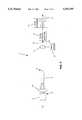
- FIG. 1is a drawing showing the principal features of a preferred embodiment of the present invention for producing high brightness pulse laser beams useful for X-ray lithography.
- FIGS. 1A, 1B and 1Care qualitative representations of the pulse shape at various stages of the embodiment shown in FIG. 1.
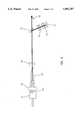
- FIG. 2is a drawing showing in greater detail a first portion of the embodiment of FIG. 1.
- FIG. 3is a drawing showing in greater detail a second portion of the embodiment shown in FIG. 1.
- FIG. 4is a drawing showing the amplifier pumping configuration using laser diodes for the embodiment shown in FIG. 1.
- FIG. 5is a drawing showing a cluster of tightly focused spots.
- FIG. 6is a drawing showing the details of the second preferred seed laser system.
- FIGS. 7A and Bare drawings showing the details of the third preferred seed laser system. They show the effect of turning on a Pockels cell.
- FIGS. 1, 2 and 3A preferred embodiment of the present invention can be described by reference to FIGS. 1, 2 and 3.
- this embodimentconsists of a mode locked Nd:YAG laser oscillator 2, a pulse spacing selector 20, a beam expander 22, a polarizing beam splitter 26, a double pass amplifier section 24 and a beam steering PZT 48 on which amplifier folding mirror 38 is mounted.
- the output of amplifier 24is focused to a tiny spot on moving copper tape target 27.
- FIG. 2describes the seed laser laser section of the embodiment which is for producing very short duration pulses at a very high repetition rate and FIGS.
- FIG. 5shows the result of a beam steering mechanism to generate a cluster of few 20 ⁇ m spots 52 over a 500 ⁇ m diameter circular area on a metal target.
- FIG. 2is a diagram of a Nd:YAG mode locked oscillator type laser device 2.
- a Nd:YAG polished rod 4(3 mm diameter and 2.5 cm long) is longitudinally pumped by a 5 bar impingement cooled laser diode array 6 (SDL part number SDL3245-J5).
- the diode pump arrayis quasi-CW and is preferably run at 20 percent duty factor (about 200 ⁇ s ON and 800 ⁇ s OFF) and 50 Watt average.
- the diode array wavelengthis at 808 nm which corresponds to strong absorption in the Nd:YAG.
- the output of the pump diodesare collimated by an array of cylindrical micro-lenses 8.
- a fast focusing lens 10concentrates the pump light at the back end of Nd:YAG crystal 4.
- the back surface of Nd:YAG crystal 4has 5 m radius of curvature (convex) and is polished and coated for maximum reflection (about 99.8 percent) at 1064 nm (the lasing wavelength of the Nd:YAG laser) and for at least 85 percent transmission for 808 nm (the pump wavelength).
- the pump lightis trapped in the laser rod via total internal reflection (similar to a fiber optics) for high pumping efficiency.
- the front surface 12 of the Nd:YAG rodis cut at 2 degrees to avoid parasitic oscillations and AR coated for minimal insertion loses at 1064 nm.
- a Brewster cut acousto-optic mode locker 14(Brimrose Corporation of America Model FSML-38-10-BR-1064) is placed next to a partially transmitting mirror 16 (output coupler) to actively force all the longitudinal modes to be in phase each time they pass the mode locker.
- the RF carrier frequency (f) of the mode locker and the optical length of the laser resonator (L)must relate as follows:
- cis the speed of light.
- a train of mode locked pulses at 76 MHz (due to the standing waves that form in the acousto-optic cell) during the ON timewill be obtained.
- the pulse durationwill be about 100 ps with an energy per pulse of about 0.6 ⁇ J.
- the time interval between pulses during the 200 ⁇ s diode ON periodsis about 13 ns. During each ON period we get about 15,200 of these very short pulses. Then we have a dead time of about 800 ⁇ s before the next series of 15,200 short pulses.
- FIG. 1AA qualitative depiction of this pulse train is shown in FIG. 1A.
- the rapid series of pulsesrepresent 15,200 pulses each with an energy of about 0.6 ⁇ J per pulse spread over 200 ⁇ s and the space represents an 800 ⁇ s dead time.
- Pulse spacing selector 20consists in this embodiment of an electro-optic modulator such as Model 305 supplied by ConOptics. This unit will function as a fast shutter to pass light from the beam during short intervals (each interval having a duration of about 10 ns) at a frequency of 60,000 Hz.
- the pulse selector(synchronized with the beam) will pass a single pulse through each 10 ns window and block all other pulses. At our frequency of 60,000 Hz, we will therefore have about 12 pulses pass each 200 ⁇ s ON period. Since we have 1,000 of these ON periods each second, we will get about 12,000 pulses per second.
- the output of pulse spacing selector 20is a pulse train consisting of clumps of about 12 pulses (each pulse having a duration of about 100 ps) spaced over 200 ⁇ s duration and these clumps of short pulses being spaced at intervals of 1,000 per second. This is an average of 12,000 pulses per second. To summarize, the output of pulse spacing selector is as follows:
- FIG. 1BA qualitative depiction of this pulse train is shown graphically in FIG. 1B. It is essentially the same as the train shown in FIG. 1A except the frequency of the pulses during the ON period has been reduced by a factor of about 1,260.
- the output of the pulse spacing selectoris expanded from a cross section of about 0.07 cm 2 to a cross section of about 0.6 cm 2 with a 3:1 beam expander 22 as shown in FIG. 2.
- Beam expander 22consist of an appropriate combination of lenses or any of several commercially available beam expanders chosen for the 1064 nm Nd:YAG beam.
- the output of beam expander 22is directed to amplifier 24 as shown in FIG. 1.
- amplifier 24for this preferred embodiment is shown if FIG. 1. Two-pass amplification is shown in FIG. 3 and our preferred pumping configuration is shown in FIG. 4. The amplifier must boost the seed beam energy to the mJ/pulse level.
- FIG. 3shows the principal features of the amplifier other than the amplifier pumping equipment.
- the linearly polarized beam 21 from beam expanderpasses through a thin film polarizing beam splitter 26 and into a first Nd:YAG amplifier rod 28 then through a one half wavelength rotator 30 (to cancel thermally induced bi-refringence) then through a second Nd:YAG amplifier rod 32 then through quarter wave plate 34 (for shifting the polarization of the outgoing beam by 90 degrees) and corrector lens 36 (for correcting the thermal lensing in the Nd rods) and is reflected off high reflectivity (HR) mirror 38.
- HRhigh reflectivity
- the beampasses back through the elements of amplifier 24 for two pass amplification and reflected off polarizing beam splitter 26 from which the beam is focused and directed to a metal target 27 as shown in FIG. 1.
- the amplifier pumping equipmentis shown in FIG. 4.
- This equipmentincludes 64 modules of 50 Watt per module (nominal) laser diode arrays 40 for a total of about 3 kW average power operating at 808 nm wavelength, 20 percent duty factor (200 ⁇ s ON and 800 ⁇ s OFF).
- 16 setsare arranged (4 shown in the circumferential direction and 4 in the linear direction, not shown) as indicated in FIG. 4.
- the output of the diode lasersare directed into the Nd:YAG rods 28 and 32 with cylindrical lenses 42 and the rods are water cooled by water jacket 44 as shown in FIG. 4.
- Amplifier 24provides a 1.3 ⁇ 10 5 amplification of the input beam with good preservation of the input beam (near diffraction limited beam, less than or equal to 2XDL).
- the output of Amplifier 24is a pulsed laser beam with the following characteristics:
- FIG. 1CA qualitative description of the output of the amplifier is shown in FIG. 1C. It is substantially the same as the pulse train shown in FIG. 1B except the pulses are amplified in energy by a factor of about 133,000. We then focus the beam to a 20 ILm spot on the target.
- Preferred sizes of the X-ray point source for proximity lithographyis in the range of a few 100 ⁇ m (e.g., 500 ⁇ m)in diameter to about 1 mm in diameter.
- a 500 ⁇ m spot simulated from 20 ⁇ m diameter pulsesis shown in FIG. 5.
- we have to hit the target at different spotse.g., multiple 20 ⁇ m spots 52 spread over a 500 ⁇ m area 50. This is accomplished in this embodiment by mounting a mirror 38 on fast two-axis PZT 48 that steers the beam slightly over the required area as shown in FIG. 1
- An additional approach to the seed lasercan be a Q-switch mode locked configuration or a Q-switch mode locked with cavity dumping configuration (FIG. 6).
- Laser diode array 61 with ⁇ -lenses 63is focused by lens 65 for end pumping of the Nd:YAG rod 67 as described in the preferred embodiment.
- Polarizer beam splitter 71reflects the laser S polarization to form a folded cavity (resonator) which includes the mode locker 75 as previously described, an acousto optics Q-switch 73, and a ⁇ /4 electro optics Pockels cell 69 such as 1041 FV-106 and 5046 driver (Fast Pulse Technologies) for cavity dumping.
- Polarizer beam splitter 71(highly transmissive to P polarization) then transmits the pulse to provide the output seed beam 79.
- This seed lasercan be substituted for the oscillator 2 and the pulse spacing selector 20 shown in FIG. 1.
- the outputis directed to beam expander 22 and the rest of the path of the beam is as shown in FIG. 1. Since the entire stored energy in the Nd rod is used to generate the short pulse (about 100 ps) output beam, energies in the few mJ per pulse (vs. 0.6 ⁇ J/p as described in the first preferred seed laser) can be obtained from this configuration.
- FIGS. 7A and BA drawing of a third preferred seed laser is shown is FIGS. 7A and B.
- Thisis a seed laser which generates a laser beam of sub nanosecond pulse duration at more than 1000 pulses per second.
- a laser cavityis formed by high reflectivity mirror 91 and coating 83 applied to the backside of Nd:YAG crystal 5.
- a polarizer beam splitter 89 and a short and fast ⁇ /2 Pockels cell 87allow for cavity dumping.
- the oscillating beam 97 shown in FIG. 7Ais P polarized in the plane of the paper due to the orientation of polarizer 89.
- When high voltage is applied to Pockels cell 87the cell will rotate the polarization of the beam to the left by 90 degrees (perpendicular to the plane of the paper).
- the polarizing beam splitter 89will reflect the perpendicular polarization as shown in FIG. 7B.
- the resultis that a pulse, equal in length of twice the distance L (between the Pockels cell 87 and the HR coatings 83), is directed to amplifier system 96 which can be the system shown in FIG. 1 other than oscillator 2 and pulse spacing selector 20. It is easy to achieve L ⁇ s of 2 to 4 cm.
- the time duration of the pulsewill be:
- the pump beamcan be CW or quasi CW.
- the first preferred seed laserwe could choose a much shorter pulse duration than 100 ps. These could be obtained using a passive saturable absorber instead of the acousto-optic mode locker. With a saturable absorber we can get femtosecond pulses. It is our belief that the advantage of pulses in the 100 ps range is that we get some heating of the plasma whereas the very very short pulses creates the plasma but provides very little heating of it.
- the energy per pulseneeds to be in the range of 80 mJ/pulse when the objective lens is about 12 cm from the target. A distance of at least 12 cm is recommended to avoid contaminating the lens with target material. However, if this distance is reduced the required energy per pulse could be reduced accordingly because we could focus on a smaller spot. By doing so we could reduce the energy per pulse requirement from about 80 mJ/pulse to as low as about 10 mJ/pulse.
- the cost of laser diodes for pumping solid state lasersis primarily dominated by the peak power requirements and this determines the number of diode bars.
- the barsBy operating the bars at a relatively high duty factor of 20 percent and generating a large number of pulses per second, we can minimize the initial cost of the diode pumping system. For example, a 1 kW system may require 3 kW average power from the pump diodes, a 20 percent duty factor diode array system would require 15 kW peak power. Using 50 Watt peak bars at $700 per bar, the system would cost $210,000. In comparison, a 1 percent duty factor system would require 300 kW peak power. The cost would be $4,000,000.
- the first preferred seed beam pulse train frequencycould be in the range of 10 MHz to 200 MHz or greater. With some compromise in the average power the number of pulses per second could be reduced down to about 1,000 Hz.
- the amplifiercan be of slab or rod design.
- the solid state materialcan be of a host material other than Nd:YAG.
- Nd:YLF, Cr:LiSAF, Ti:S, etc.could be used.
- Amplification needed to boost the seed beam to the mJ/pulse levelcan be satisfied by either high gain or multiple passes. Up to eight passes can be done with passive components and much higher number of passes can be done in a regenerative amplifier.
- the steering mirror in the amplifiercan be any reflecting element that would be appropriate to generate the cluster of spot sizes desired, such as the 20 ⁇ m spots.
- the electro-optic modulatorfor pulse spacing, such as cavity dumping or even an optical rotary interrupter.
- the pulse spacing deviceswould in most applications remove a very large percentage of the pulses in the first preferred seed beam such as more than 99 percent as in the preferred embodiment described; however, We could imagine applications where as the percentage remove might be as low as 80 percent. Accordingly the reader is requested to determine the scope of the invention by the appended claims and their legal equivalents, and not by the given examples.
Landscapes
- Physics & Mathematics (AREA)
- Electromagnetism (AREA)
- Engineering & Computer Science (AREA)
- Optics & Photonics (AREA)
- Plasma & Fusion (AREA)
- Lasers (AREA)
Abstract
Description
f=c/4L
______________________________________ Pulse duration about 100 ps Energy per pulse 0.6 μJ Peak power perpulse 6 kW Average frequency 12,000 pulses per second Average power 7.2 mW Beam cross section 0.07 cm.sup.2 ______________________________________
______________________________________ Pulse duration about 100 ps Energy per pulse 80 mJ/pulse Peak power per pulse 800 MW Average frequency 12,000 pulses per second Average power 1 kW Beam diameter 9 mm Brightness (power/pulse) 2.5 × 10.sup.14 Watts/cm.sup.2 (20 μm dia. spot) ______________________________________
t=2L/c
Claims (30)
Priority Applications (10)
| Application Number | Priority Date | Filing Date | Title |
|---|---|---|---|
| US08/339,755US5491707A (en) | 1994-08-24 | 1994-11-15 | Low cost, high average power, high brightness solid state laser |
| US08/434,860US5539764A (en) | 1994-08-24 | 1995-05-04 | Laser generated X-ray source |
| EP95944024AEP0792530B1 (en) | 1994-11-15 | 1995-11-06 | Low cost, high average power, high brightness solid state laser |
| PCT/US1995/014258WO1996016484A1 (en) | 1994-11-15 | 1995-11-06 | Low cost, high average power, high brightness solid state laser |
| DE69532479TDE69532479T2 (en) | 1994-11-15 | 1995-11-06 | INEXPENSIVE SOLID LASER WITH HIGH MEDIUM PERFORMANCE AND HIGH BRIGHTNESS |
| JP8516895AJPH10509280A (en) | 1994-11-15 | 1995-11-06 | Low cost, high average power, high brightness solid state laser |
| KR1019970703260AKR100371125B1 (en) | 1994-11-15 | 1995-11-06 | Solid-state pulse laser system with low average power and high luminance |
| US08/725,750US5742634A (en) | 1994-08-24 | 1996-10-04 | Picosecond laser |
| US08/845,185US5790574A (en) | 1994-08-24 | 1997-04-21 | Low cost, high average power, high brightness solid state laser |
| US09/058,274US6016324A (en) | 1994-08-24 | 1998-04-09 | Short pulse laser system |
Applications Claiming Priority (2)
| Application Number | Priority Date | Filing Date | Title |
|---|---|---|---|
| US08/295,283US5434875A (en) | 1994-08-24 | 1994-08-24 | Low cost, high average power, high brightness solid state laser |
| US08/339,755US5491707A (en) | 1994-08-24 | 1994-11-15 | Low cost, high average power, high brightness solid state laser |
Related Parent Applications (1)
| Application Number | Title | Priority Date | Filing Date |
|---|---|---|---|
| US08/295,283Continuation-In-PartUS5434875A (en) | 1994-08-24 | 1994-08-24 | Low cost, high average power, high brightness solid state laser |
Related Child Applications (3)
| Application Number | Title | Priority Date | Filing Date |
|---|---|---|---|
| US08/434,860Continuation-In-PartUS5539764A (en) | 1994-08-24 | 1995-05-04 | Laser generated X-ray source |
| US50337395AContinuation-In-Part | 1994-08-24 | 1995-07-17 | |
| US09/058,274Continuation-In-PartUS6016324A (en) | 1994-08-24 | 1998-04-09 | Short pulse laser system |
Publications (1)
| Publication Number | Publication Date |
|---|---|
| US5491707Atrue US5491707A (en) | 1996-02-13 |
Family
ID=26969030
Family Applications (1)
| Application Number | Title | Priority Date | Filing Date |
|---|---|---|---|
| US08/339,755Expired - LifetimeUS5491707A (en) | 1994-08-24 | 1994-11-15 | Low cost, high average power, high brightness solid state laser |
Country Status (1)
| Country | Link |
|---|---|
| US (1) | US5491707A (en) |
Cited By (26)
| Publication number | Priority date | Publication date | Assignee | Title |
|---|---|---|---|---|
| US5692004A (en)* | 1993-02-23 | 1997-11-25 | Electro Optic Systems Pty. Ltd. | Laser adaptable to lightweight construction |
| WO1998022995A3 (en)* | 1996-10-04 | 1998-10-15 | Jmar Technology Co | Picosecond laser |
| US5930282A (en)* | 1997-05-19 | 1999-07-27 | General Electric Company | Method and apparatus for adjusting the pump distribution in a laser |
| US5963575A (en)* | 1993-03-27 | 1999-10-05 | Clyxon Laser Fur Mediziner GmbH | Q-switched laser system, in particular for laser lithotripsy |
| EP0949730A3 (en)* | 1998-04-09 | 2001-04-04 | Jmar Technology Company | Short pulse laser system |
| US6272156B1 (en)* | 1998-01-28 | 2001-08-07 | Coherent, Inc. | Apparatus for ultrashort pulse transportation and delivery |
| US6389101B1 (en) | 1999-05-24 | 2002-05-14 | Jmar Research, Inc. | Parallel x-ray nanotomography |
| EP1341274A1 (en)* | 2002-03-01 | 2003-09-03 | GSI Lumonics Ltd. | Laser apparatus |
| KR100415126B1 (en)* | 1998-07-02 | 2004-01-14 | 제너럴 스캐닝, 인코포레이티드 | Controlling laser polarization |
| US20040052278A1 (en)* | 2001-08-10 | 2004-03-18 | Lightwave Electronics Corporation | Fiber amplifier system for producing visible light |
| US6807198B1 (en)* | 1999-07-07 | 2004-10-19 | Femtolasers Produktions Gmbh | Laser device |
| US20050058163A1 (en)* | 2003-09-12 | 2005-03-17 | Lightwave Electronics Corporation | High repetition rate passively Q-switched laser for blue laser based on interactions in fiber |
| US20050180043A1 (en)* | 2003-12-17 | 2005-08-18 | Jmar Research Inc. | Systems and methods for tape advancement in laser produced plasma equipment |
| US20050211910A1 (en)* | 2004-03-29 | 2005-09-29 | Jmar Research, Inc. | Morphology and Spectroscopy of Nanoscale Regions using X-Rays Generated by Laser Produced Plasma |
| WO2005081372A3 (en)* | 2004-02-20 | 2005-12-08 | Powerlase Ltd | Laser multiplexing |
| EP1617530A2 (en) | 2004-07-14 | 2006-01-18 | High Q Laser Production GmbH | Pulse train generator and method for generating a repeating sequence of laser pulses |
| US20060067476A1 (en)* | 2004-07-27 | 2006-03-30 | Jmar Research, Inc. | Rotating shutter for laser-produced plasma debris mitigation |
| US7082149B1 (en)* | 2003-06-24 | 2006-07-25 | Photonics Industries Int'l | High power diode side pumped solid state laser |
| US20060262815A1 (en)* | 2005-05-23 | 2006-11-23 | Time-Bandwidth Products Ag | Light pulse generating apparatus and method |
| US20070195322A1 (en)* | 2005-10-11 | 2007-08-23 | Jmar Research, Inc. | Multipulse agile laser source for real time spark spectrochemical hazard analysis |
| EP1483812A4 (en)* | 2002-02-19 | 2008-06-18 | Gsi Group Ltd | Methods and systems for laser processing a workpiece and methods and apparatus for controlling beam quality therein |
| US20080240347A1 (en)* | 2005-07-22 | 2008-10-02 | Jmar Research, Inc. | Method, apparatus, and system for extending depth of field (dof) in a short-wavelength microscope using wavefront encoding |
| USRE42499E1 (en) | 1997-01-23 | 2011-06-28 | Coherent, Inc. | System and method for amplifying an optical pulse and pumping laser therefor |
| CN102882110A (en)* | 2012-09-13 | 2013-01-16 | 北京国科世纪激光技术有限公司 | Device for amplifying medium/large-aperture laser |
| US20130242380A1 (en)* | 2012-03-16 | 2013-09-19 | Kla-Tencor Corporation | Suppression Of Parasitic Optical Feedback In Pulse Laser Systems |
| CN104733991B (en)* | 2014-09-17 | 2018-08-31 | 中国电子科技集团公司第十一研究所 | A kind of passive mode-locking slab laser |
Citations (5)
| Publication number | Priority date | Publication date | Assignee | Title |
|---|---|---|---|---|
| US4630275A (en)* | 1984-12-10 | 1986-12-16 | Allied Corporation | Controlled slow Q-switch |
| US4646308A (en)* | 1985-09-30 | 1987-02-24 | Spectra-Physics, Inc. | Synchronously pumped dye laser using ultrashort pump pulses |
| US4930901A (en)* | 1988-12-23 | 1990-06-05 | Electro Scientific Industries, Inc. | Method of and apparatus for modulating a laser beam |
| US5140600A (en)* | 1990-11-28 | 1992-08-18 | Lambda Physik Gesellschaft Zur Herstellung Von Lasern Mbh | Method of controlling the total energy amount of a plurality of laser pulses |
| US5339323A (en)* | 1993-04-30 | 1994-08-16 | Lumonics Corporation | Laser system for controlling emitted pulse energy |
- 1994
- 1994-11-15USUS08/339,755patent/US5491707A/ennot_activeExpired - Lifetime
Patent Citations (5)
| Publication number | Priority date | Publication date | Assignee | Title |
|---|---|---|---|---|
| US4630275A (en)* | 1984-12-10 | 1986-12-16 | Allied Corporation | Controlled slow Q-switch |
| US4646308A (en)* | 1985-09-30 | 1987-02-24 | Spectra-Physics, Inc. | Synchronously pumped dye laser using ultrashort pump pulses |
| US4930901A (en)* | 1988-12-23 | 1990-06-05 | Electro Scientific Industries, Inc. | Method of and apparatus for modulating a laser beam |
| US5140600A (en)* | 1990-11-28 | 1992-08-18 | Lambda Physik Gesellschaft Zur Herstellung Von Lasern Mbh | Method of controlling the total energy amount of a plurality of laser pulses |
| US5339323A (en)* | 1993-04-30 | 1994-08-16 | Lumonics Corporation | Laser system for controlling emitted pulse energy |
Cited By (36)
| Publication number | Priority date | Publication date | Assignee | Title |
|---|---|---|---|---|
| US5692004A (en)* | 1993-02-23 | 1997-11-25 | Electro Optic Systems Pty. Ltd. | Laser adaptable to lightweight construction |
| US5963575A (en)* | 1993-03-27 | 1999-10-05 | Clyxon Laser Fur Mediziner GmbH | Q-switched laser system, in particular for laser lithotripsy |
| WO1998022995A3 (en)* | 1996-10-04 | 1998-10-15 | Jmar Technology Co | Picosecond laser |
| USRE42499E1 (en) | 1997-01-23 | 2011-06-28 | Coherent, Inc. | System and method for amplifying an optical pulse and pumping laser therefor |
| US5930282A (en)* | 1997-05-19 | 1999-07-27 | General Electric Company | Method and apparatus for adjusting the pump distribution in a laser |
| US6272156B1 (en)* | 1998-01-28 | 2001-08-07 | Coherent, Inc. | Apparatus for ultrashort pulse transportation and delivery |
| EP0949730A3 (en)* | 1998-04-09 | 2001-04-04 | Jmar Technology Company | Short pulse laser system |
| KR100415126B1 (en)* | 1998-07-02 | 2004-01-14 | 제너럴 스캐닝, 인코포레이티드 | Controlling laser polarization |
| US6389101B1 (en) | 1999-05-24 | 2002-05-14 | Jmar Research, Inc. | Parallel x-ray nanotomography |
| US6807198B1 (en)* | 1999-07-07 | 2004-10-19 | Femtolasers Produktions Gmbh | Laser device |
| US20040052278A1 (en)* | 2001-08-10 | 2004-03-18 | Lightwave Electronics Corporation | Fiber amplifier system for producing visible light |
| US7039076B2 (en) | 2001-08-10 | 2006-05-02 | Jds Uniphase Corporation | Fiber amplifier system for producing visible light |
| EP1483812A4 (en)* | 2002-02-19 | 2008-06-18 | Gsi Group Ltd | Methods and systems for laser processing a workpiece and methods and apparatus for controlling beam quality therein |
| EP1341274A1 (en)* | 2002-03-01 | 2003-09-03 | GSI Lumonics Ltd. | Laser apparatus |
| US7082149B1 (en)* | 2003-06-24 | 2006-07-25 | Photonics Industries Int'l | High power diode side pumped solid state laser |
| US7116687B2 (en) | 2003-09-12 | 2006-10-03 | Jds Uniphase Corporation | High repetition rate passively Q-switched laser for blue laser based on interactions in fiber |
| US20050058163A1 (en)* | 2003-09-12 | 2005-03-17 | Lightwave Electronics Corporation | High repetition rate passively Q-switched laser for blue laser based on interactions in fiber |
| US20050180043A1 (en)* | 2003-12-17 | 2005-08-18 | Jmar Research Inc. | Systems and methods for tape advancement in laser produced plasma equipment |
| US7424096B2 (en) | 2003-12-17 | 2008-09-09 | Jmar Research, Inc. | Systems and methods for tape advancement in laser produced plasma equipment |
| WO2005081372A3 (en)* | 2004-02-20 | 2005-12-08 | Powerlase Ltd | Laser multiplexing |
| US20070272669A1 (en)* | 2004-02-20 | 2007-11-29 | Comley Andrew J | Laser Multiplexing |
| US20050211910A1 (en)* | 2004-03-29 | 2005-09-29 | Jmar Research, Inc. | Morphology and Spectroscopy of Nanoscale Regions using X-Rays Generated by Laser Produced Plasma |
| EP1617530A2 (en) | 2004-07-14 | 2006-01-18 | High Q Laser Production GmbH | Pulse train generator and method for generating a repeating sequence of laser pulses |
| US20060067476A1 (en)* | 2004-07-27 | 2006-03-30 | Jmar Research, Inc. | Rotating shutter for laser-produced plasma debris mitigation |
| US7302043B2 (en) | 2004-07-27 | 2007-11-27 | Gatan, Inc. | Rotating shutter for laser-produced plasma debris mitigation |
| US20060262815A1 (en)* | 2005-05-23 | 2006-11-23 | Time-Bandwidth Products Ag | Light pulse generating apparatus and method |
| US7386019B2 (en) | 2005-05-23 | 2008-06-10 | Time-Bandwidth Products Ag | Light pulse generating apparatus and method |
| WO2006125333A1 (en)* | 2005-05-23 | 2006-11-30 | Time-Bandwidth Products Ag | Cw-pumped multipass amplifier for a sliced train of mode-locked laser pulses |
| US20080240347A1 (en)* | 2005-07-22 | 2008-10-02 | Jmar Research, Inc. | Method, apparatus, and system for extending depth of field (dof) in a short-wavelength microscope using wavefront encoding |
| US20070195322A1 (en)* | 2005-10-11 | 2007-08-23 | Jmar Research, Inc. | Multipulse agile laser source for real time spark spectrochemical hazard analysis |
| US7688443B2 (en) | 2005-10-11 | 2010-03-30 | Jmar Llc | Multipulse agile laser source for real time spark spectrochemical hazard analysis |
| US20130242380A1 (en)* | 2012-03-16 | 2013-09-19 | Kla-Tencor Corporation | Suppression Of Parasitic Optical Feedback In Pulse Laser Systems |
| US8767291B2 (en)* | 2012-03-16 | 2014-07-01 | Kla-Tencor Corporation | Suppression of parasitic optical feedback in pulse laser systems |
| CN102882110A (en)* | 2012-09-13 | 2013-01-16 | 北京国科世纪激光技术有限公司 | Device for amplifying medium/large-aperture laser |
| CN102882110B (en)* | 2012-09-13 | 2015-07-01 | 北京国科世纪激光技术有限公司 | Device for amplifying medium/large-aperture laser |
| CN104733991B (en)* | 2014-09-17 | 2018-08-31 | 中国电子科技集团公司第十一研究所 | A kind of passive mode-locking slab laser |
Similar Documents
| Publication | Publication Date | Title |
|---|---|---|
| US5434875A (en) | Low cost, high average power, high brightness solid state laser | |
| US5491707A (en) | Low cost, high average power, high brightness solid state laser | |
| US5790574A (en) | Low cost, high average power, high brightness solid state laser | |
| US5689363A (en) | Long-pulse-width narrow-bandwidth solid state laser | |
| US6016324A (en) | Short pulse laser system | |
| KR100339057B1 (en) | Short pulse laser system | |
| US5673281A (en) | Solid state system for frequency conversion using raman-active media and non-linear media | |
| US5539764A (en) | Laser generated X-ray source | |
| US5644424A (en) | Laser amplifier and method | |
| US5280491A (en) | Two dimensional scan amplifier laser | |
| EP0792530B1 (en) | Low cost, high average power, high brightness solid state laser | |
| US20080037597A1 (en) | Laser Apparatus | |
| JP2003524872A (en) | Repetitive-pulse solid-state laser with a cavity with many different gain media | |
| KR20210114400A (en) | Diode Pumped Solid State Laser Device for Laser Annealing | |
| JP3465478B2 (en) | Optical parametric oscillator | |
| JP2007529903A (en) | LPP EUV light source | |
| US5612967A (en) | Two dimensional scan amplifier laser | |
| US20070019688A1 (en) | Infra-red multi-wavelength laser source | |
| US6108357A (en) | Single head laser oscillator-amplifier | |
| US8446925B2 (en) | Reduction of timing jitter in a passive Q-switched solid state laser | |
| Apollonov | High power disk laser | |
| CN107069414A (en) | Minimize hundred picosecond laser beauty instruments | |
| JP3700516B2 (en) | Wavelength conversion laser device and laser processing device | |
| Apollonov | High power disk lasers: advantages and prospects | |
| US10852621B1 (en) | System and method for generating multiple simultaneous, co-propagating wavelengths via nonlinear wavelength conversion |
Legal Events
| Date | Code | Title | Description |
|---|---|---|---|
| AS | Assignment | Owner name:JAMAR TECHNOLOGIES CO., CALIFORNIA Free format text:ASSIGNMENT OF ASSIGNORS INTEREST;ASSIGNORS:REIGER, HARRY;SHIELDS, HARRY;FOSTER, RICHARD M.;REEL/FRAME:007218/0945 Effective date:19941108 | |
| STCF | Information on status: patent grant | Free format text:PATENTED CASE | |
| FPAY | Fee payment | Year of fee payment:4 | |
| FPAY | Fee payment | Year of fee payment:8 | |
| AS | Assignment | Owner name:LAURUS MASTER FUND, LTD., NEW YORK Free format text:GRANT OF SECURITY INTEREST IN PATENTS AND TRADEMARKS;ASSIGNOR:JMAR RESEARCH, INC. (F/K/A JAMAR TECHNOLOGY CO. AND F/K/A JMAR TECHNOLOGY CO., A DELAWARE CORPORATION);REEL/FRAME:019224/0176 Effective date:20070411 | |
| FPAY | Fee payment | Year of fee payment:12 | |
| AS | Assignment | Owner name:LV ADMINISTRATIVE SERVICES, INC., NEW YORK Free format text:SECURITY AGREEMENT;ASSIGNORS:JMAR TECHNOLOGIES, INC.;JMAR RESEARCH, INC.;REEL/FRAME:022440/0281 Effective date:20080925 Owner name:LV ADMINISTRATIVE SERVICES, INC.,NEW YORK Free format text:SECURITY AGREEMENT;ASSIGNORS:JMAR TECHNOLOGIES, INC.;JMAR RESEARCH, INC.;REEL/FRAME:022440/0281 Effective date:20080925 | |
| AS | Assignment | Owner name:JMAR RESEARCH, INC., CALIFORNIA Free format text:CHANGE OF NAME;ASSIGNOR:JMAR TECHNOLOGY CO.;REEL/FRAME:022597/0503 Effective date:19980507 Owner name:JMAR TECHNOLOGY CO., CALIFORNIA Free format text:CHANGE OF NAME;ASSIGNOR:JAMAR TECHNOLOGY CO.;REEL/FRAME:022597/0498 Effective date:19950221 | |
| AS | Assignment | Owner name:JAMAR TECHNOLOGY CO., CALIFORNIA Free format text:CORRECTIVE ASSIGNMENT TO CORRECT THE ASSIGNEE PREVIOUSLY RECORDED ON REEL 007218 FRAME 0945;ASSIGNORS:REIGER, HARRY;SHIELDS, HARRY;FOSTER, RICHARD M.;REEL/FRAME:022597/0817 Effective date:19941108 | |
| AS | Assignment | Owner name:JMAR, LLC, A DELAWARE LIMITED LIABILITY COMPANY, C Free format text:ASSIGNMENT OF ASSIGNORS INTEREST;ASSIGNORS:JMAR TECHNOLOGIES, INC., A DELAWARE CORPORATION;JMAR RESEARCH, INC., A CALIFORNIA CORPORATION;JMAR/SAL NANOLITHOGRAPHY, INC., A CALIFORNIA CORPORATION;AND OTHERS;REEL/FRAME:022645/0804 Effective date:20090506 Owner name:JMAR, LLC, A DELAWARE LIMITED LIABILITY COMPANY,CA Free format text:ASSIGNMENT OF ASSIGNORS INTEREST;ASSIGNORS:JMAR TECHNOLOGIES, INC., A DELAWARE CORPORATION;JMAR RESEARCH, INC., A CALIFORNIA CORPORATION;JMAR/SAL NANOLITHOGRAPHY, INC., A CALIFORNIA CORPORATION;AND OTHERS;REEL/FRAME:022645/0804 Effective date:20090506 | |
| AS | Assignment | Owner name:LV ADMINISTRATIVE SERVICES, INC., NEW YORK Free format text:INTELLECTUAL PROPERTY SECURITY AGREEMENT;ASSIGNOR:JMAR, LLC;REEL/FRAME:022659/0864 Effective date:20090507 Owner name:LV ADMINISTRATIVE SERVICES, INC.,NEW YORK Free format text:INTELLECTUAL PROPERTY SECURITY AGREEMENT;ASSIGNOR:JMAR, LLC;REEL/FRAME:022659/0864 Effective date:20090507 |