US5491303A - Surface mount interposer - Google Patents
Surface mount interposerDownload PDFInfo
- Publication number
- US5491303A US5491303AUS08/210,509US21050994AUS5491303AUS 5491303 AUS5491303 AUS 5491303AUS 21050994 AUS21050994 AUS 21050994AUS 5491303 AUS5491303 AUS 5491303A
- Authority
- US
- United States
- Prior art keywords
- printed circuit
- solder
- interposer
- solder pads
- pads
- Prior art date
- Legal status (The legal status is an assumption and is not a legal conclusion. Google has not performed a legal analysis and makes no representation as to the accuracy of the status listed.)
- Expired - Fee Related
Links
- 229910000679solderInorganic materials0.000claimsabstractdescription51
- 239000000758substrateSubstances0.000claimsabstractdescription11
- 239000000463materialSubstances0.000claimsdescription9
- 239000011521glassSubstances0.000claimsdescription2
- 238000005476solderingMethods0.000abstractdescription2
- 150000003071polychlorinated biphenylsChemical class0.000description18
- 238000010276constructionMethods0.000description3
- RYGMFSIKBFXOCR-UHFFFAOYSA-NCopperChemical compound[Cu]RYGMFSIKBFXOCR-UHFFFAOYSA-N0.000description2
- 229910052802copperInorganic materials0.000description2
- 239000010949copperSubstances0.000description2
- 238000000034methodMethods0.000description2
- 229920001721polyimidePolymers0.000description2
- 230000035882stressEffects0.000description2
- 239000004593EpoxySubstances0.000description1
- 239000004642PolyimideSubstances0.000description1
- 238000005253claddingMethods0.000description1
- 230000008602contractionEffects0.000description1
- 238000000151depositionMethods0.000description1
- 230000000694effectsEffects0.000description1
- 238000005516engineering processMethods0.000description1
- 239000003822epoxy resinSubstances0.000description1
- 239000004744fabricSubstances0.000description1
- 239000003365glass fiberSubstances0.000description1
- 238000003780insertionMethods0.000description1
- 230000037431insertionEffects0.000description1
- 239000011159matrix materialSubstances0.000description1
- 238000012986modificationMethods0.000description1
- 230000004048modificationEffects0.000description1
- 238000007747platingMethods0.000description1
- 229920000647polyepoxidePolymers0.000description1
- 239000009719polyimide resinSubstances0.000description1
- 238000007639printingMethods0.000description1
- 239000011347resinSubstances0.000description1
- 229920005989resinPolymers0.000description1
- 238000006467substitution reactionMethods0.000description1
- 230000008646thermal stressEffects0.000description1
Images

Classifications
- H—ELECTRICITY
- H05—ELECTRIC TECHNIQUES NOT OTHERWISE PROVIDED FOR
- H05K—PRINTED CIRCUITS; CASINGS OR CONSTRUCTIONAL DETAILS OF ELECTRIC APPARATUS; MANUFACTURE OF ASSEMBLAGES OF ELECTRICAL COMPONENTS
- H05K3/00—Apparatus or processes for manufacturing printed circuits
- H05K3/30—Assembling printed circuits with electric components, e.g. with resistor
- H05K3/32—Assembling printed circuits with electric components, e.g. with resistor electrically connecting electric components or wires to printed circuits
- H05K3/34—Assembling printed circuits with electric components, e.g. with resistor electrically connecting electric components or wires to printed circuits by soldering
- H05K3/341—Surface mounted components
- H05K3/3431—Leadless components
- H05K3/3436—Leadless components having an array of bottom contacts, e.g. pad grid array or ball grid array components
- H—ELECTRICITY
- H05—ELECTRIC TECHNIQUES NOT OTHERWISE PROVIDED FOR
- H05K—PRINTED CIRCUITS; CASINGS OR CONSTRUCTIONAL DETAILS OF ELECTRIC APPARATUS; MANUFACTURE OF ASSEMBLAGES OF ELECTRICAL COMPONENTS
- H05K3/00—Apparatus or processes for manufacturing printed circuits
- H05K3/36—Assembling printed circuits with other printed circuits
- H05K3/368—Assembling printed circuits with other printed circuits parallel to each other
- H—ELECTRICITY
- H05—ELECTRIC TECHNIQUES NOT OTHERWISE PROVIDED FOR
- H05K—PRINTED CIRCUITS; CASINGS OR CONSTRUCTIONAL DETAILS OF ELECTRIC APPARATUS; MANUFACTURE OF ASSEMBLAGES OF ELECTRICAL COMPONENTS
- H05K2201/00—Indexing scheme relating to printed circuits covered by H05K1/00
- H05K2201/04—Assemblies of printed circuits
- H05K2201/049—PCB for one component, e.g. for mounting onto mother PCB
- H—ELECTRICITY
- H05—ELECTRIC TECHNIQUES NOT OTHERWISE PROVIDED FOR
- H05K—PRINTED CIRCUITS; CASINGS OR CONSTRUCTIONAL DETAILS OF ELECTRIC APPARATUS; MANUFACTURE OF ASSEMBLAGES OF ELECTRICAL COMPONENTS
- H05K2201/00—Indexing scheme relating to printed circuits covered by H05K1/00
- H05K2201/09—Shape and layout
- H05K2201/09209—Shape and layout details of conductors
- H05K2201/09372—Pads and lands
- H05K2201/0949—Pad close to a hole, not surrounding the hole
- H—ELECTRICITY
- H05—ELECTRIC TECHNIQUES NOT OTHERWISE PROVIDED FOR
- H05K—PRINTED CIRCUITS; CASINGS OR CONSTRUCTIONAL DETAILS OF ELECTRIC APPARATUS; MANUFACTURE OF ASSEMBLAGES OF ELECTRICAL COMPONENTS
- H05K2201/00—Indexing scheme relating to printed circuits covered by H05K1/00
- H05K2201/10—Details of components or other objects attached to or integrated in a printed circuit board
- H05K2201/10227—Other objects, e.g. metallic pieces
- H05K2201/10378—Interposers
- H—ELECTRICITY
- H05—ELECTRIC TECHNIQUES NOT OTHERWISE PROVIDED FOR
- H05K—PRINTED CIRCUITS; CASINGS OR CONSTRUCTIONAL DETAILS OF ELECTRIC APPARATUS; MANUFACTURE OF ASSEMBLAGES OF ELECTRICAL COMPONENTS
- H05K2201/00—Indexing scheme relating to printed circuits covered by H05K1/00
- H05K2201/10—Details of components or other objects attached to or integrated in a printed circuit board
- H05K2201/10431—Details of mounted components
- H05K2201/10439—Position of a single component
- H05K2201/10477—Inverted
- H—ELECTRICITY
- H05—ELECTRIC TECHNIQUES NOT OTHERWISE PROVIDED FOR
- H05K—PRINTED CIRCUITS; CASINGS OR CONSTRUCTIONAL DETAILS OF ELECTRIC APPARATUS; MANUFACTURE OF ASSEMBLAGES OF ELECTRICAL COMPONENTS
- H05K2201/00—Indexing scheme relating to printed circuits covered by H05K1/00
- H05K2201/10—Details of components or other objects attached to or integrated in a printed circuit board
- H05K2201/10613—Details of electrical connections of non-printed components, e.g. special leads
- H05K2201/10621—Components characterised by their electrical contacts
- H05K2201/10734—Ball grid array [BGA]; Bump grid array
- Y—GENERAL TAGGING OF NEW TECHNOLOGICAL DEVELOPMENTS; GENERAL TAGGING OF CROSS-SECTIONAL TECHNOLOGIES SPANNING OVER SEVERAL SECTIONS OF THE IPC; TECHNICAL SUBJECTS COVERED BY FORMER USPC CROSS-REFERENCE ART COLLECTIONS [XRACs] AND DIGESTS
- Y02—TECHNOLOGIES OR APPLICATIONS FOR MITIGATION OR ADAPTATION AGAINST CLIMATE CHANGE
- Y02P—CLIMATE CHANGE MITIGATION TECHNOLOGIES IN THE PRODUCTION OR PROCESSING OF GOODS
- Y02P70/00—Climate change mitigation technologies in the production process for final industrial or consumer products
- Y02P70/50—Manufacturing or production processes characterised by the final manufactured product
Definitions
- This inventionrelates in general to interconnection means, and more particularly to printed circuit board interconnectors.
- PCBprinted circuit board
- Those having multiple circuit boardstypically interconnect the PCBs by some means.
- this connectionhas taken the form of discrete wires, wiring harnesses, flex circuit interconnections, card edge connectors, zero insertion force (ZIF) connectors, plugs, etc.
- ZIFzero insertion force
- Each of these connectionshas served a purpose, and each has one or more advantages.
- eachalso has a disadvantage.
- discrete wires, wiring harnesses, and flex circuit interconnectiontypically cannot connect the two PCBs closely together nor can they maintain the PCBs in fixed alignment. Discrete wires require expensive and time consuming manual labor to assemble.
- Card edge connectors, ZIF connectors, and plugsare better at maintaining fixed alignment, but typically require considerable space in the vertical direction, require assembly labor, and are costly.
- the advent of surface mount technologyhas further exacerbated the need for low cost, small connectors that can easily interconnect multiple PCBs and hold them in fixed relationship to one another, while requiring minimal vertical space.
- an interposerfor connecting two or more printed circuit boards.
- the interposeris a circuit-carrying substrate with two or more solder pads on each of the two sides. Each of the solder pads are connected to an electrically conductive via in the substrate, providing electrical interconnection from one side to the other side. Each solder pad has a solder bump on it.
- a circuit assemblyis made by soldering the solder bumps on one side of the interposer to corresponding solder pads on a printed circuit board.
- the solder bumps on the other side of the interposerare likewise soldered to the corresponding solder pads of a second printed circuit board.
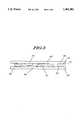
- FIG. 1is a plan view of an interposer in accordance with the invention.
- FIG. 2is a cross-sectional view of FIG. 1 through section 2--2.
- FIG. 3is a side view of an assembly made using by connecting two printed circuit boards with an interposer in accordance with the invention.
- an interposer 100is made using a substrate 102, such as a printed circuit board made from epoxy or polyimide resins.
- the resinis reinforced with a woven glass cloth or other matrix such as chopped glass fibers.
- This constructionis the same as that commonly used in the industry for conventional PCBs.
- the material used for the interposeris the same as that used in the printed circuit boards that are to be interconnected. This provides the advantage of reducing the stresses between the PCBs and the interposer, as will be explained later.
- a first plurality or set of surface mount pads 104are formed in a pattern that is a mirror image of the pads on one of the PCBs that are to be connected. These pads are formed in a conventional manner, for example, by subtractive processing of copper clad laminates. The reader will appreciate that the pattern of surface mount pads can take many forms, and need not be limited to the configuration shown in the drawing.
- Each of the padsis connected to a corresponding plated through hole or via 106 in the substrate. The hole typically passes straight through the substrate, but other constructions such as blind or buried vias that only extend part way through may also be successfully used.
- the interconnectionis completed by using another blind or buried via connected to an inner layer of circuitry in the substrate, making the interposer a three layer configuration.
- the inner layercan also be used as a ground layer, providing a shielding effect for the two PCBs.
- the important criteriais that an electrical connection be made from one side 105 of the interposer to the other side 107.
- the drawingshows that the pad 104 is remote from the via 106, and is connected to the via by a conductive trace 204.
- Other configurations, such as the pad located directly on top of the via or adjacent to the viacan also be used and still fall within the scope of the invention. Referring to FIG. 2, on the other or second side 107 of the interposed, another series of surface mount solder pads 109 is formed.
- This second set of pads 109resembles the pattern to be connected on the second PCB.
- Each of the second set of padsis also connected to a respective via 106 in a manner similar to one of the configurations described above with the first set of pads 104.
- This schemeresults in each of the first set of pads 104 on one side 105 being electrically connected to one of the pads 109 in the second set on the other side 107 of the PCB.
- What separates the interposer of the instant invention from a conventional PCBis the fact that the interposer only has connections for the solder pads, and does not provide other functions such as mounting sites for components or holes for components.
- the interposeris shown in the drawing figures as a rectangular part, the reader will readily appreciate that it could be made in many different shapes, such as an "L”, "C”, or window frame shape.
- solder pads 104, 109 on both sides of the interposerhas a solder ball or solder bump 108 formed on the pad.
- the solder bumps 108provide the means to electrically and mechanically connect the two PCBs together.
- the solder bumpis formed using any number of methods such as printing solder paste, using solder preforms, by plating or cladding solder, or by depositing solder spheres on the pads. In each of the methods, the solder material is reflowed to ensure that the solder material is firmly adhered to the underlying copper pad. After reflow, the solder material usually assumes the shape of a modified sphere, as shown in the drawing. With the addition of the solder bumps 108, the interposer 100 is now complete, and ready for use.
- the solder bumps 108 on the first side 105 of the interposerare aligned to the solder pads on a first PCB 302 and are reflowed.
- Each of the solder bumps 108 on the second side 107 of the interposeris also aligned to one of the solder pads on the second PCB 304 and reflowed.
- This arrangementprovides a direct and robust electrical and mechanical connection between each of the solder pads on the first PCB 302 and each of the solder pads on the second PCB 304. It can be seen that one advantage of this type of configuration is that the interposer also provides structural rigidity to the assembled structure, and also holds each PCB in fixed alignment to the other.
- the two PCBs 302, 304are interconnected very closely and do not require any more vertical space than would normally be required for the components 310 themselves. This allows the two PCBs to be mated close together, allowing smaller products to be made. More than two PCBs can be connected together using the interposer. For example, three PCBs can be vertically connected using two interposers. The concept can be further extended to couple many PCBs together vertically.
- PCBscan be mated together with minimal vertical height, the PCBs can be held in fixed relationship to each other, and structural rigidity is provided.
- the interposercan be inexpensively made, and custom configurations are readily available, because the pattern of pads and holes is easily changed.
Landscapes
- Engineering & Computer Science (AREA)
- Manufacturing & Machinery (AREA)
- Microelectronics & Electronic Packaging (AREA)
- Combinations Of Printed Boards (AREA)
Abstract
Description
Claims (5)
Priority Applications (1)
| Application Number | Priority Date | Filing Date | Title |
|---|---|---|---|
| US08/210,509US5491303A (en) | 1994-03-21 | 1994-03-21 | Surface mount interposer |
Applications Claiming Priority (1)
| Application Number | Priority Date | Filing Date | Title |
|---|---|---|---|
| US08/210,509US5491303A (en) | 1994-03-21 | 1994-03-21 | Surface mount interposer |
Publications (1)
| Publication Number | Publication Date |
|---|---|
| US5491303Atrue US5491303A (en) | 1996-02-13 |
Family
ID=22783188
Family Applications (1)
| Application Number | Title | Priority Date | Filing Date |
|---|---|---|---|
| US08/210,509Expired - Fee RelatedUS5491303A (en) | 1994-03-21 | 1994-03-21 | Surface mount interposer |
Country Status (1)
| Country | Link |
|---|---|
| US (1) | US5491303A (en) |
Cited By (66)
| Publication number | Priority date | Publication date | Assignee | Title |
|---|---|---|---|---|
| US5716222A (en)* | 1995-11-03 | 1998-02-10 | Advanced Interconnections Corporation | Ball grid array including modified hard ball contacts and apparatus for attaching hard ball contacts to a ball grid array |
| US5825631A (en)* | 1997-04-16 | 1998-10-20 | Starkey Laboratories | Method for connecting two substrates in a thick film hybrid circuit |
| US5895281A (en)* | 1997-08-27 | 1999-04-20 | The Whitaker Corporation | High density board to board connector |
| US5953816A (en)* | 1997-07-16 | 1999-09-21 | General Dynamics Information Systems, Inc. | Process of making interposers for land grip arrays |
| US6024584A (en)* | 1996-10-10 | 2000-02-15 | Berg Technology, Inc. | High density connector |
| US6042389A (en)* | 1996-10-10 | 2000-03-28 | Berg Technology, Inc. | Low profile connector |
| US6050832A (en)* | 1998-08-07 | 2000-04-18 | Fujitsu Limited | Chip and board stress relief interposer |
| US6093035A (en)* | 1996-06-28 | 2000-07-25 | Berg Technology, Inc. | Contact for use in an electrical connector |
| US6139336A (en)* | 1996-11-14 | 2000-10-31 | Berg Technology, Inc. | High density connector having a ball type of contact surface |
| US6146203A (en)* | 1995-06-12 | 2000-11-14 | Berg Technology, Inc. | Low cross talk and impedance controlled electrical connector |
| FR2795285A1 (en)* | 1999-06-17 | 2000-12-22 | Nec Corp | Mounting structure for integrated circuit, providing increased mechanical and radiation integrity, interposes additional card between circuit and mounting card and employs solder ball connections |
| KR20000076944A (en)* | 1999-03-24 | 2000-12-26 | 가리쉬마 홀트라 | Circuit chip connector and method of connecting a circuit chip |
| US6241535B1 (en) | 1996-10-10 | 2001-06-05 | Berg Technology, Inc. | Low profile connector |
| US6246312B1 (en) | 2000-07-20 | 2001-06-12 | Cts Corporation | Ball grid array resistor terminator network |
| US6325644B1 (en) | 1996-10-10 | 2001-12-04 | Berg Technology, Inc. | High density connector and method of manufacture |
| US6400018B2 (en) | 1998-08-27 | 2002-06-04 | 3M Innovative Properties Company | Via plug adapter |
| WO2002030166A3 (en)* | 2000-10-04 | 2002-06-13 | Honeywell Int Inc | Compliant attachment interface |
| US6462414B1 (en) | 1999-03-05 | 2002-10-08 | Altera Corporation | Integrated circuit package utilizing a conductive structure for interlocking a conductive ball to a ball pad |
| US6472724B1 (en)* | 1999-04-19 | 2002-10-29 | Nec Corporation | Electronic device structure capable of preventing malfunction caused by electromagnetic wave coming from outside |
| US6493240B2 (en)* | 2000-05-24 | 2002-12-10 | International Business Machines Corporation | Interposer for connecting two substrates and resulting assembly |
| US6507118B1 (en) | 2000-07-14 | 2003-01-14 | 3M Innovative Properties Company | Multi-metal layer circuit |
| FR2828983A1 (en)* | 2001-08-23 | 2003-02-28 | Novatec | Interface for electric interconnection and absorption of thermo-mechanical constraints, and method for its implementation, by use of an insulator substrate with feedthroughs and solder balls |
| US6538213B1 (en)* | 2000-02-18 | 2003-03-25 | International Business Machines Corporation | High density design for organic chip carriers |
| US20030080174A1 (en)* | 2001-10-31 | 2003-05-01 | Kennedy Craig M. | Header for surface mount between parallel circuit boards |
| KR100389113B1 (en)* | 2001-06-21 | 2003-06-25 | 주식회사 태화인서트 | Device Adhering Method for FPCB |
| EP1207727A3 (en)* | 2000-11-16 | 2003-08-13 | International Business Machines Corporation | Compliant laminate connector |
| US6622905B2 (en)* | 2000-12-29 | 2003-09-23 | Intel Corporation | Design and assembly methodology for reducing bridging in bonding electronic components to pads connected to vias |
| US20030183420A1 (en)* | 2002-03-26 | 2003-10-02 | Dishongh Terrance J. | Circuit board with via through surface mount device contact |
| US6674008B2 (en)* | 1999-12-16 | 2004-01-06 | Oki Electric Industry Co., Ltd. | Cross substrate, method of mounting semiconductor element, and semiconductor device |
| US20040020044A1 (en)* | 2002-07-30 | 2004-02-05 | Ashman John J. | Apparatus and method for making electrical connectors |
| US6750404B1 (en)* | 1998-12-23 | 2004-06-15 | Nortel Networks Limited | High density printed wiring board having in-via surface mounting, pads |
| US20050003171A1 (en)* | 2003-02-06 | 2005-01-06 | R-Tec Corporation | Plated via interposer |
| US20050023662A1 (en)* | 2003-03-11 | 2005-02-03 | Bolken Todd O. | Techniques for packaging a multiple device component |
| US20050024839A1 (en)* | 2003-07-31 | 2005-02-03 | Bloom Terry R. | Ball grid array package |
| US6851954B2 (en) | 2002-07-30 | 2005-02-08 | Avx Corporation | Electrical connectors and electrical components |
| US20050035450A1 (en)* | 2003-08-13 | 2005-02-17 | David Poole | Ball grid array package having testing capability after mounting |
| US6860741B2 (en) | 2002-07-30 | 2005-03-01 | Avx Corporation | Apparatus and methods for retaining and placing electrical components |
| US6939173B1 (en) | 1995-06-12 | 2005-09-06 | Fci Americas Technology, Inc. | Low cross talk and impedance controlled electrical connector with solder masses |
| US20050221675A1 (en)* | 2003-07-16 | 2005-10-06 | Rathburn James J | Fine pitch electrical interconnect assembly |
| EP1303171A3 (en)* | 2001-10-11 | 2005-11-16 | Alps Electric Co., Ltd. | Electronic circuit unit suitable for miniaturization |
| US20060035483A1 (en)* | 2003-07-16 | 2006-02-16 | Gryphics, Inc. | Fine pitch electrical interconnect assembly |
| US20070115645A1 (en)* | 2001-08-17 | 2007-05-24 | Jacobsen Jeffrey J | Apparatuses and methods for forming wireless RF labels |
| US20070117268A1 (en)* | 2005-11-23 | 2007-05-24 | Baker Hughes, Inc. | Ball grid attachment |
| US7250330B2 (en)* | 2002-10-29 | 2007-07-31 | International Business Machines Corporation | Method of making an electronic package |
| US20080182436A1 (en)* | 2003-07-16 | 2008-07-31 | Gryphics, Inc. | Fine pitch electrical interconnect assembly |
| US20080185726A1 (en)* | 2007-02-01 | 2008-08-07 | Siliconware Precision Industries Co., Ltd. | Semiconductor package substrate |
| US7446399B1 (en) | 2004-08-04 | 2008-11-04 | Altera Corporation | Pad structures to improve board-level reliability of solder-on-pad BGA structures |
| US20100327439A1 (en)* | 2007-05-08 | 2010-12-30 | Tae-Joo Hwang | Semiconductor package and method of forming the same |
| US8044502B2 (en) | 2006-03-20 | 2011-10-25 | Gryphics, Inc. | Composite contact for fine pitch electrical interconnect assembly |
| WO2013044198A1 (en)* | 2011-09-25 | 2013-03-28 | Authentec, Inc. | Electronic device including finger sensor and related methods |
| USD718253S1 (en) | 2012-04-13 | 2014-11-25 | Fci Americas Technology Llc | Electrical cable connector |
| US8905651B2 (en) | 2012-01-31 | 2014-12-09 | Fci | Dismountable optical coupling device |
| USD720698S1 (en) | 2013-03-15 | 2015-01-06 | Fci Americas Technology Llc | Electrical cable connector |
| US8944831B2 (en) | 2012-04-13 | 2015-02-03 | Fci Americas Technology Llc | Electrical connector having ribbed ground plate with engagement members |
| USD727268S1 (en) | 2012-04-13 | 2015-04-21 | Fci Americas Technology Llc | Vertical electrical connector |
| USD727852S1 (en) | 2012-04-13 | 2015-04-28 | Fci Americas Technology Llc | Ground shield for a right angle electrical connector |
| US9048583B2 (en) | 2009-03-19 | 2015-06-02 | Fci Americas Technology Llc | Electrical connector having ribbed ground plate |
| USD733662S1 (en) | 2013-01-25 | 2015-07-07 | Fci Americas Technology Llc | Connector housing for electrical connector |
| USD746236S1 (en) | 2012-07-11 | 2015-12-29 | Fci Americas Technology Llc | Electrical connector housing |
| US9257778B2 (en) | 2012-04-13 | 2016-02-09 | Fci Americas Technology | High speed electrical connector |
| US9543703B2 (en) | 2012-07-11 | 2017-01-10 | Fci Americas Technology Llc | Electrical connector with reduced stack height |
| US20170179080A1 (en)* | 2015-12-18 | 2017-06-22 | Intel Corporation | Semiconductor package interposer having encapsulated interconnects |
| US10993325B2 (en) | 2019-07-31 | 2021-04-27 | Abb Power Electronics Inc. | Interposer printed circuit boards for power modules |
| US11006524B2 (en) | 2017-09-08 | 2021-05-11 | Apple Inc. | Circuit board interposer |
| CN113301726A (en)* | 2021-05-25 | 2021-08-24 | 中国电子科技集团公司第二十九研究所 | Design method and welding method of printed board assembly based on vertical interconnection among boards |
| US11490517B2 (en) | 2019-07-31 | 2022-11-01 | ABB Power Electronics, Inc. | Interposer printed circuit boards for power modules |
Citations (3)
| Publication number | Priority date | Publication date | Assignee | Title |
|---|---|---|---|---|
| US4642889A (en)* | 1985-04-29 | 1987-02-17 | Amp Incorporated | Compliant interconnection and method therefor |
| US5218761A (en)* | 1991-04-08 | 1993-06-15 | Nec Corporation | Process for manufacturing printed wiring boards |
| US5258648A (en)* | 1991-06-27 | 1993-11-02 | Motorola, Inc. | Composite flip chip semiconductor device with an interposer having test contacts formed along its periphery |
- 1994
- 1994-03-21USUS08/210,509patent/US5491303A/ennot_activeExpired - Fee Related
Patent Citations (3)
| Publication number | Priority date | Publication date | Assignee | Title |
|---|---|---|---|---|
| US4642889A (en)* | 1985-04-29 | 1987-02-17 | Amp Incorporated | Compliant interconnection and method therefor |
| US5218761A (en)* | 1991-04-08 | 1993-06-15 | Nec Corporation | Process for manufacturing printed wiring boards |
| US5258648A (en)* | 1991-06-27 | 1993-11-02 | Motorola, Inc. | Composite flip chip semiconductor device with an interposer having test contacts formed along its periphery |
Cited By (120)
| Publication number | Priority date | Publication date | Assignee | Title |
|---|---|---|---|---|
| US6939173B1 (en) | 1995-06-12 | 2005-09-06 | Fci Americas Technology, Inc. | Low cross talk and impedance controlled electrical connector with solder masses |
| US6146203A (en)* | 1995-06-12 | 2000-11-14 | Berg Technology, Inc. | Low cross talk and impedance controlled electrical connector |
| US5716222A (en)* | 1995-11-03 | 1998-02-10 | Advanced Interconnections Corporation | Ball grid array including modified hard ball contacts and apparatus for attaching hard ball contacts to a ball grid array |
| US6093035A (en)* | 1996-06-28 | 2000-07-25 | Berg Technology, Inc. | Contact for use in an electrical connector |
| US6358068B1 (en) | 1996-10-10 | 2002-03-19 | Fci Americas Technology, Inc. | Stress resistant connector and method for reducing stress in housing thereof |
| US7186123B2 (en) | 1996-10-10 | 2007-03-06 | Fci Americas Technology, Inc. | High density connector and method of manufacture |
| US8167630B2 (en) | 1996-10-10 | 2012-05-01 | Fci Americas Technology Llc | High density connector and method of manufacture |
| US6079991A (en)* | 1996-10-10 | 2000-06-27 | Berg Technology, Inc. | Method for placing contact on electrical connector |
| US6024584A (en)* | 1996-10-10 | 2000-02-15 | Berg Technology, Inc. | High density connector |
| US20050079763A1 (en)* | 1996-10-10 | 2005-04-14 | Lemke Timothy A. | High density connector and method of manufacture |
| US20060068635A1 (en)* | 1996-10-10 | 2006-03-30 | Lemke Timothy A | High density connector and method of manufacture |
| US20080032524A1 (en)* | 1996-10-10 | 2008-02-07 | Lemke Timothy A | High Density Connector and Method of Manufacture |
| US7168964B2 (en)* | 1996-10-10 | 2007-01-30 | Fci Americas Technology, Inc. | High density connector and method of manufacture |
| US6164983A (en)* | 1996-10-10 | 2000-12-26 | Berg Technology, Inc. | High density connector |
| US6241535B1 (en) | 1996-10-10 | 2001-06-05 | Berg Technology, Inc. | Low profile connector |
| US7476110B2 (en) | 1996-10-10 | 2009-01-13 | Fci Americas Technology, Inc. | High density connector and method of manufacture |
| US6042389A (en)* | 1996-10-10 | 2000-03-28 | Berg Technology, Inc. | Low profile connector |
| US6325644B1 (en) | 1996-10-10 | 2001-12-04 | Berg Technology, Inc. | High density connector and method of manufacture |
| US6247635B1 (en) | 1996-11-14 | 2001-06-19 | Berg Technology, Inc. | High density connector having a ball type of contact surface |
| US6139336A (en)* | 1996-11-14 | 2000-10-31 | Berg Technology, Inc. | High density connector having a ball type of contact surface |
| US5825631A (en)* | 1997-04-16 | 1998-10-20 | Starkey Laboratories | Method for connecting two substrates in a thick film hybrid circuit |
| US5953816A (en)* | 1997-07-16 | 1999-09-21 | General Dynamics Information Systems, Inc. | Process of making interposers for land grip arrays |
| US5895281A (en)* | 1997-08-27 | 1999-04-20 | The Whitaker Corporation | High density board to board connector |
| US6050832A (en)* | 1998-08-07 | 2000-04-18 | Fujitsu Limited | Chip and board stress relief interposer |
| US6400018B2 (en) | 1998-08-27 | 2002-06-04 | 3M Innovative Properties Company | Via plug adapter |
| US6864577B2 (en) | 1998-08-27 | 2005-03-08 | 3M Innovative Properties Company | Via plug adapter |
| US6750404B1 (en)* | 1998-12-23 | 2004-06-15 | Nortel Networks Limited | High density printed wiring board having in-via surface mounting, pads |
| US6929978B2 (en) | 1999-03-05 | 2005-08-16 | Altera Corporation | Method of fabricating an integrated circuit package utilizing a conductive structure for improving the bond strength between an IC package and a printed circuit board |
| US6462414B1 (en) | 1999-03-05 | 2002-10-08 | Altera Corporation | Integrated circuit package utilizing a conductive structure for interlocking a conductive ball to a ball pad |
| US20020194731A1 (en)* | 1999-03-05 | 2002-12-26 | Altera Corporation | Fabrication method and structure of an integrated circuit package |
| KR20000076944A (en)* | 1999-03-24 | 2000-12-26 | 가리쉬마 홀트라 | Circuit chip connector and method of connecting a circuit chip |
| US6472724B1 (en)* | 1999-04-19 | 2002-10-29 | Nec Corporation | Electronic device structure capable of preventing malfunction caused by electromagnetic wave coming from outside |
| FR2795285A1 (en)* | 1999-06-17 | 2000-12-22 | Nec Corp | Mounting structure for integrated circuit, providing increased mechanical and radiation integrity, interposes additional card between circuit and mounting card and employs solder ball connections |
| US20040074660A1 (en)* | 1999-12-16 | 2004-04-22 | Akio Nakamura | Cross substrate, method of mounting semiconductor element, and semiconductor device |
| US6674008B2 (en)* | 1999-12-16 | 2004-01-06 | Oki Electric Industry Co., Ltd. | Cross substrate, method of mounting semiconductor element, and semiconductor device |
| US6797881B2 (en) | 1999-12-16 | 2004-09-28 | Oki Electric Industry Co., Ltd. | Cross substrate, method of mounting semiconductor element, and semiconductor device |
| US6538213B1 (en)* | 2000-02-18 | 2003-03-25 | International Business Machines Corporation | High density design for organic chip carriers |
| SG99347A1 (en)* | 2000-02-18 | 2003-10-27 | Ibm | High density design for organic chip carriers |
| US6493240B2 (en)* | 2000-05-24 | 2002-12-10 | International Business Machines Corporation | Interposer for connecting two substrates and resulting assembly |
| US6507118B1 (en) | 2000-07-14 | 2003-01-14 | 3M Innovative Properties Company | Multi-metal layer circuit |
| US6246312B1 (en) | 2000-07-20 | 2001-06-12 | Cts Corporation | Ball grid array resistor terminator network |
| WO2002030166A3 (en)* | 2000-10-04 | 2002-06-13 | Honeywell Int Inc | Compliant attachment interface |
| EP1207727A3 (en)* | 2000-11-16 | 2003-08-13 | International Business Machines Corporation | Compliant laminate connector |
| US6622905B2 (en)* | 2000-12-29 | 2003-09-23 | Intel Corporation | Design and assembly methodology for reducing bridging in bonding electronic components to pads connected to vias |
| KR100389113B1 (en)* | 2001-06-21 | 2003-06-25 | 주식회사 태화인서트 | Device Adhering Method for FPCB |
| US7559486B2 (en) | 2001-08-17 | 2009-07-14 | Alien Technology Corporation | Apparatuses and methods for forming wireless RF labels |
| US20070115645A1 (en)* | 2001-08-17 | 2007-05-24 | Jacobsen Jeffrey J | Apparatuses and methods for forming wireless RF labels |
| FR2828983A1 (en)* | 2001-08-23 | 2003-02-28 | Novatec | Interface for electric interconnection and absorption of thermo-mechanical constraints, and method for its implementation, by use of an insulator substrate with feedthroughs and solder balls |
| EP1303171A3 (en)* | 2001-10-11 | 2005-11-16 | Alps Electric Co., Ltd. | Electronic circuit unit suitable for miniaturization |
| US20030080174A1 (en)* | 2001-10-31 | 2003-05-01 | Kennedy Craig M. | Header for surface mount between parallel circuit boards |
| US6803527B2 (en)* | 2002-03-26 | 2004-10-12 | Intel Corporation | Circuit board with via through surface mount device contact |
| US20030183420A1 (en)* | 2002-03-26 | 2003-10-02 | Dishongh Terrance J. | Circuit board with via through surface mount device contact |
| US6851954B2 (en) | 2002-07-30 | 2005-02-08 | Avx Corporation | Electrical connectors and electrical components |
| US6860741B2 (en) | 2002-07-30 | 2005-03-01 | Avx Corporation | Apparatus and methods for retaining and placing electrical components |
| US20040020044A1 (en)* | 2002-07-30 | 2004-02-05 | Ashman John J. | Apparatus and method for making electrical connectors |
| US6928727B2 (en) | 2002-07-30 | 2005-08-16 | Avx Corporation | Apparatus and method for making electrical connectors |
| US7250330B2 (en)* | 2002-10-29 | 2007-07-31 | International Business Machines Corporation | Method of making an electronic package |
| US20050003171A1 (en)* | 2003-02-06 | 2005-01-06 | R-Tec Corporation | Plated via interposer |
| US20050023662A1 (en)* | 2003-03-11 | 2005-02-03 | Bolken Todd O. | Techniques for packaging a multiple device component |
| US7804171B2 (en)* | 2003-03-11 | 2010-09-28 | Micron Technology, Inc. | Techniques for packaging a multiple device component |
| US7537461B2 (en) | 2003-07-16 | 2009-05-26 | Gryphics, Inc. | Fine pitch electrical interconnect assembly |
| US20060035483A1 (en)* | 2003-07-16 | 2006-02-16 | Gryphics, Inc. | Fine pitch electrical interconnect assembly |
| US7422439B2 (en) | 2003-07-16 | 2008-09-09 | Gryphics, Inc. | Fine pitch electrical interconnect assembly |
| US7297003B2 (en) | 2003-07-16 | 2007-11-20 | Gryphics, Inc. | Fine pitch electrical interconnect assembly |
| US7326064B2 (en) | 2003-07-16 | 2008-02-05 | Gryphics, Inc. | Fine pitch electrical interconnect assembly |
| US20050221675A1 (en)* | 2003-07-16 | 2005-10-06 | Rathburn James J | Fine pitch electrical interconnect assembly |
| US20080182436A1 (en)* | 2003-07-16 | 2008-07-31 | Gryphics, Inc. | Fine pitch electrical interconnect assembly |
| US20070164433A1 (en)* | 2003-07-31 | 2007-07-19 | Bloom Terry R | Ball grid array package |
| US7180186B2 (en) | 2003-07-31 | 2007-02-20 | Cts Corporation | Ball grid array package |
| US20050024839A1 (en)* | 2003-07-31 | 2005-02-03 | Bloom Terry R. | Ball grid array package |
| US6946733B2 (en) | 2003-08-13 | 2005-09-20 | Cts Corporation | Ball grid array package having testing capability after mounting |
| US20050035450A1 (en)* | 2003-08-13 | 2005-02-17 | David Poole | Ball grid array package having testing capability after mounting |
| US7446399B1 (en) | 2004-08-04 | 2008-11-04 | Altera Corporation | Pad structures to improve board-level reliability of solder-on-pad BGA structures |
| US20070117268A1 (en)* | 2005-11-23 | 2007-05-24 | Baker Hughes, Inc. | Ball grid attachment |
| US8232632B2 (en) | 2006-03-20 | 2012-07-31 | R&D Sockets, Inc. | Composite contact for fine pitch electrical interconnect assembly |
| US8044502B2 (en) | 2006-03-20 | 2011-10-25 | Gryphics, Inc. | Composite contact for fine pitch electrical interconnect assembly |
| US7808110B2 (en)* | 2007-02-01 | 2010-10-05 | Siliconware Precision Industries Co., Ltd. | Semiconductor package substrate |
| US20080185726A1 (en)* | 2007-02-01 | 2008-08-07 | Siliconware Precision Industries Co., Ltd. | Semiconductor package substrate |
| US8421244B2 (en)* | 2007-05-08 | 2013-04-16 | Samsung Electronics Co., Ltd. | Semiconductor package and method of forming the same |
| US20100327439A1 (en)* | 2007-05-08 | 2010-12-30 | Tae-Joo Hwang | Semiconductor package and method of forming the same |
| US8736035B2 (en)* | 2007-05-08 | 2014-05-27 | Samsung Electronics Co. Ltd. | Semiconductor package and method of forming the same |
| US9484292B2 (en) | 2007-05-08 | 2016-11-01 | Samsung Electronics Co. Ltd. | Semiconductor package and method of forming the same |
| US9685400B2 (en) | 2007-05-08 | 2017-06-20 | Samsung Electronics Co., Ltd. | Semiconductor package and method of forming the same |
| US9461410B2 (en) | 2009-03-19 | 2016-10-04 | Fci Americas Technology Llc | Electrical connector having ribbed ground plate |
| US9048583B2 (en) | 2009-03-19 | 2015-06-02 | Fci Americas Technology Llc | Electrical connector having ribbed ground plate |
| US10720721B2 (en) | 2009-03-19 | 2020-07-21 | Fci Usa Llc | Electrical connector having ribbed ground plate |
| US10096921B2 (en) | 2009-03-19 | 2018-10-09 | Fci Usa Llc | Electrical connector having ribbed ground plate |
| CN103827890A (en)* | 2011-09-25 | 2014-05-28 | 奥森泰克公司 | Electronic device including finger sensor and related methods |
| CN103827890B (en)* | 2011-09-25 | 2017-07-28 | 苹果公司 | Electronic equipment and correlation technique including finger sensor |
| US8836478B2 (en) | 2011-09-25 | 2014-09-16 | Authentec, Inc. | Electronic device including finger sensor and related methods |
| WO2013044198A1 (en)* | 2011-09-25 | 2013-03-28 | Authentec, Inc. | Electronic device including finger sensor and related methods |
| AU2012312082B2 (en)* | 2011-09-25 | 2015-10-22 | Apple Inc. | Electronic device including finger sensor and related methods |
| US8905651B2 (en) | 2012-01-31 | 2014-12-09 | Fci | Dismountable optical coupling device |
| USD790471S1 (en) | 2012-04-13 | 2017-06-27 | Fci Americas Technology Llc | Vertical electrical connector |
| USD718253S1 (en) | 2012-04-13 | 2014-11-25 | Fci Americas Technology Llc | Electrical cable connector |
| USD748063S1 (en) | 2012-04-13 | 2016-01-26 | Fci Americas Technology Llc | Electrical ground shield |
| US9257778B2 (en) | 2012-04-13 | 2016-02-09 | Fci Americas Technology | High speed electrical connector |
| USD750025S1 (en) | 2012-04-13 | 2016-02-23 | Fci Americas Technology Llc | Vertical electrical connector |
| USD750030S1 (en) | 2012-04-13 | 2016-02-23 | Fci Americas Technology Llc | Electrical cable connector |
| USD816044S1 (en) | 2012-04-13 | 2018-04-24 | Fci Americas Technology Llc | Electrical cable connector |
| US9831605B2 (en) | 2012-04-13 | 2017-11-28 | Fci Americas Technology Llc | High speed electrical connector |
| US8944831B2 (en) | 2012-04-13 | 2015-02-03 | Fci Americas Technology Llc | Electrical connector having ribbed ground plate with engagement members |
| USD727268S1 (en) | 2012-04-13 | 2015-04-21 | Fci Americas Technology Llc | Vertical electrical connector |
| USD727852S1 (en) | 2012-04-13 | 2015-04-28 | Fci Americas Technology Llc | Ground shield for a right angle electrical connector |
| US9543703B2 (en) | 2012-07-11 | 2017-01-10 | Fci Americas Technology Llc | Electrical connector with reduced stack height |
| USD746236S1 (en) | 2012-07-11 | 2015-12-29 | Fci Americas Technology Llc | Electrical connector housing |
| US9871323B2 (en) | 2012-07-11 | 2018-01-16 | Fci Americas Technology Llc | Electrical connector with reduced stack height |
| USD751507S1 (en) | 2012-07-11 | 2016-03-15 | Fci Americas Technology Llc | Electrical connector |
| USD772168S1 (en) | 2013-01-25 | 2016-11-22 | Fci Americas Technology Llc | Connector housing for electrical connector |
| USD733662S1 (en) | 2013-01-25 | 2015-07-07 | Fci Americas Technology Llc | Connector housing for electrical connector |
| USD745852S1 (en) | 2013-01-25 | 2015-12-22 | Fci Americas Technology Llc | Electrical connector |
| USD766832S1 (en) | 2013-01-25 | 2016-09-20 | Fci Americas Technology Llc | Electrical connector |
| USD720698S1 (en) | 2013-03-15 | 2015-01-06 | Fci Americas Technology Llc | Electrical cable connector |
| US20170179080A1 (en)* | 2015-12-18 | 2017-06-22 | Intel Corporation | Semiconductor package interposer having encapsulated interconnects |
| US11006524B2 (en) | 2017-09-08 | 2021-05-11 | Apple Inc. | Circuit board interposer |
| US10993325B2 (en) | 2019-07-31 | 2021-04-27 | Abb Power Electronics Inc. | Interposer printed circuit boards for power modules |
| US11439013B2 (en) | 2019-07-31 | 2022-09-06 | ABB Power Electronics, Inc. | Interposer printed circuit boards for power modules |
| US11490517B2 (en) | 2019-07-31 | 2022-11-01 | ABB Power Electronics, Inc. | Interposer printed circuit boards for power modules |
| CN113301726A (en)* | 2021-05-25 | 2021-08-24 | 中国电子科技集团公司第二十九研究所 | Design method and welding method of printed board assembly based on vertical interconnection among boards |
| CN113301726B (en)* | 2021-05-25 | 2022-03-08 | 中国电子科技集团公司第二十九研究所 | Design method and welding method of printed board assembly based on vertical interconnection among boards |
Similar Documents
| Publication | Publication Date | Title |
|---|---|---|
| US5491303A (en) | Surface mount interposer | |
| US6892451B2 (en) | Method of making an interposer sub-assembly in a printed wiring board | |
| EP0526107B1 (en) | Stepped multilayer interconnection apparatus and method of making the same | |
| US5593322A (en) | Leadless high density connector | |
| US6493240B2 (en) | Interposer for connecting two substrates and resulting assembly | |
| US6663399B2 (en) | Surface mount attachable land grid array connector and method of forming same | |
| EP0908976B1 (en) | High density connector system | |
| US6817870B1 (en) | Technique for interconnecting multilayer circuit boards | |
| US8446738B2 (en) | Motherboard assembly for interconnecting and distributing signals and power | |
| US4755147A (en) | Flex head connector with ground plane | |
| US6054652A (en) | Thin-film multi-layer substrate and electronic device | |
| US6171114B1 (en) | Low insertion force array connector for providing a removable high density electrical interconnect to a flexible circuit | |
| US5796592A (en) | Module mounting structure | |
| US6257904B1 (en) | Connector with BGA arrangement for connecting to PC board | |
| KR20020042711A (en) | Interposer for use in electronic packages | |
| US6608258B1 (en) | High data rate coaxial interconnect technology between printed wiring boards | |
| KR20220016236A (en) | Board structure with a different power supply circuit board | |
| US7068120B2 (en) | Electromagnetic bus coupling having an electromagnetic coupling interposer | |
| US5772450A (en) | Electrical connectors having external circuit connections | |
| US6950315B2 (en) | High frequency module mounting structure in which solder is prevented from peeling | |
| JP2000195586A (en) | Circuit board for card connector | |
| JP2581397B2 (en) | Mounting / connection board for multi-pin circuit elements | |
| EP0914697B1 (en) | Assembly of connector and printed circuit board | |
| JPH0710969U (en) | Printed board | |
| WO2006060495A1 (en) | Bga to lga interposer |
Legal Events
| Date | Code | Title | Description |
|---|---|---|---|
| AS | Assignment | Owner name:MOTOROLA, INC., ILLINOIS Free format text:ASSIGNMENT OF ASSIGNORS INTEREST;ASSIGNOR:WEISS, MICHAEL L.;REEL/FRAME:006944/0846 Effective date:19940314 | |
| FPAY | Fee payment | Year of fee payment:4 | |
| FPAY | Fee payment | Year of fee payment:8 | |
| AS | Assignment | Owner name:FREESCALE SEMICONDUCTOR, INC., TEXAS Free format text:ASSIGNMENT OF ASSIGNORS INTEREST;ASSIGNOR:MOTOROLA, INC.;REEL/FRAME:015698/0657 Effective date:20040404 Owner name:FREESCALE SEMICONDUCTOR, INC.,TEXAS Free format text:ASSIGNMENT OF ASSIGNORS INTEREST;ASSIGNOR:MOTOROLA, INC.;REEL/FRAME:015698/0657 Effective date:20040404 | |
| AS | Assignment | Owner name:CITIBANK, N.A. AS COLLATERAL AGENT, NEW YORK Free format text:SECURITY AGREEMENT;ASSIGNORS:FREESCALE SEMICONDUCTOR, INC.;FREESCALE ACQUISITION CORPORATION;FREESCALE ACQUISITION HOLDINGS CORP.;AND OTHERS;REEL/FRAME:018855/0129 Effective date:20061201 Owner name:CITIBANK, N.A. AS COLLATERAL AGENT,NEW YORK Free format text:SECURITY AGREEMENT;ASSIGNORS:FREESCALE SEMICONDUCTOR, INC.;FREESCALE ACQUISITION CORPORATION;FREESCALE ACQUISITION HOLDINGS CORP.;AND OTHERS;REEL/FRAME:018855/0129 Effective date:20061201 | |
| REMI | Maintenance fee reminder mailed | ||
| LAPS | Lapse for failure to pay maintenance fees | ||
| STCH | Information on status: patent discontinuation | Free format text:PATENT EXPIRED DUE TO NONPAYMENT OF MAINTENANCE FEES UNDER 37 CFR 1.362 | |
| FP | Lapsed due to failure to pay maintenance fee | Effective date:20080213 | |
| AS | Assignment | Owner name:FREESCALE SEMICONDUCTOR, INC., TEXAS Free format text:PATENT RELEASE;ASSIGNOR:CITIBANK, N.A., AS COLLATERAL AGENT;REEL/FRAME:037354/0225 Effective date:20151207 |