US5489804A - Flexible preformed planar structures for interposing between a chip and a substrate - Google Patents
Flexible preformed planar structures for interposing between a chip and a substrateDownload PDFInfo
- Publication number
- US5489804A US5489804AUS08/106,157US10615793AUS5489804AUS 5489804 AUS5489804 AUS 5489804AUS 10615793 AUS10615793 AUS 10615793AUS 5489804 AUS5489804 AUS 5489804A
- Authority
- US
- United States
- Prior art keywords
- planar structure
- substrate
- preformed planar
- chip
- holes
- Prior art date
- Legal status (The legal status is an assumption and is not a legal conclusion. Google has not performed a legal analysis and makes no representation as to the accuracy of the status listed.)
- Expired - Lifetime
Links
Images


Classifications
- G—PHYSICS
- G03—PHOTOGRAPHY; CINEMATOGRAPHY; ANALOGOUS TECHNIQUES USING WAVES OTHER THAN OPTICAL WAVES; ELECTROGRAPHY; HOLOGRAPHY
- G03F—PHOTOMECHANICAL PRODUCTION OF TEXTURED OR PATTERNED SURFACES, e.g. FOR PRINTING, FOR PROCESSING OF SEMICONDUCTOR DEVICES; MATERIALS THEREFOR; ORIGINALS THEREFOR; APPARATUS SPECIALLY ADAPTED THEREFOR
- G03F7/00—Photomechanical, e.g. photolithographic, production of textured or patterned surfaces, e.g. printing surfaces; Materials therefor, e.g. comprising photoresists; Apparatus specially adapted therefor
- G03F7/70—Microphotolithographic exposure; Apparatus therefor
- G03F7/70425—Imaging strategies, e.g. for increasing throughput or resolution, printing product fields larger than the image field or compensating lithography- or non-lithography errors, e.g. proximity correction, mix-and-match, stitching or double patterning
- G03F7/70433—Layout for increasing efficiency or for compensating imaging errors, e.g. layout of exposure fields for reducing focus errors; Use of mask features for increasing efficiency or for compensating imaging errors
- H—ELECTRICITY
- H01—ELECTRIC ELEMENTS
- H01L—SEMICONDUCTOR DEVICES NOT COVERED BY CLASS H10
- H01L21/00—Processes or apparatus adapted for the manufacture or treatment of semiconductor or solid state devices or of parts thereof
- H01L21/02—Manufacture or treatment of semiconductor devices or of parts thereof
- H01L21/04—Manufacture or treatment of semiconductor devices or of parts thereof the devices having potential barriers, e.g. a PN junction, depletion layer or carrier concentration layer
- H01L21/50—Assembly of semiconductor devices using processes or apparatus not provided for in a single one of the groups H01L21/18 - H01L21/326 or H10D48/04 - H10D48/07 e.g. sealing of a cap to a base of a container
- H01L21/56—Encapsulations, e.g. encapsulation layers, coatings
- H01L21/563—Encapsulation of active face of flip-chip device, e.g. underfilling or underencapsulation of flip-chip, encapsulation preform on chip or mounting substrate
- H—ELECTRICITY
- H01—ELECTRIC ELEMENTS
- H01L—SEMICONDUCTOR DEVICES NOT COVERED BY CLASS H10
- H01L24/00—Arrangements for connecting or disconnecting semiconductor or solid-state bodies; Methods or apparatus related thereto
- H01L24/01—Means for bonding being attached to, or being formed on, the surface to be connected, e.g. chip-to-package, die-attach, "first-level" interconnects; Manufacturing methods related thereto
- H01L24/26—Layer connectors, e.g. plate connectors, solder or adhesive layers; Manufacturing methods related thereto
- H01L24/28—Structure, shape, material or disposition of the layer connectors prior to the connecting process
- H01L24/29—Structure, shape, material or disposition of the layer connectors prior to the connecting process of an individual layer connector
- H—ELECTRICITY
- H01—ELECTRIC ELEMENTS
- H01L—SEMICONDUCTOR DEVICES NOT COVERED BY CLASS H10
- H01L24/00—Arrangements for connecting or disconnecting semiconductor or solid-state bodies; Methods or apparatus related thereto
- H01L24/80—Methods for connecting semiconductor or other solid state bodies using means for bonding being attached to, or being formed on, the surface to be connected
- H01L24/81—Methods for connecting semiconductor or other solid state bodies using means for bonding being attached to, or being formed on, the surface to be connected using a bump connector
- H—ELECTRICITY
- H05—ELECTRIC TECHNIQUES NOT OTHERWISE PROVIDED FOR
- H05K—PRINTED CIRCUITS; CASINGS OR CONSTRUCTIONAL DETAILS OF ELECTRIC APPARATUS; MANUFACTURE OF ASSEMBLAGES OF ELECTRICAL COMPONENTS
- H05K3/00—Apparatus or processes for manufacturing printed circuits
- H05K3/30—Assembling printed circuits with electric components, e.g. with resistor
- H05K3/32—Assembling printed circuits with electric components, e.g. with resistor electrically connecting electric components or wires to printed circuits
- H05K3/34—Assembling printed circuits with electric components, e.g. with resistor electrically connecting electric components or wires to printed circuits by soldering
- H05K3/341—Surface mounted components
- H05K3/3431—Leadless components
- H05K3/3436—Leadless components having an array of bottom contacts, e.g. pad grid array or ball grid array components
- H—ELECTRICITY
- H10—SEMICONDUCTOR DEVICES; ELECTRIC SOLID-STATE DEVICES NOT OTHERWISE PROVIDED FOR
- H10F—INORGANIC SEMICONDUCTOR DEVICES SENSITIVE TO INFRARED RADIATION, LIGHT, ELECTROMAGNETIC RADIATION OF SHORTER WAVELENGTH OR CORPUSCULAR RADIATION
- H10F77/00—Constructional details of devices covered by this subclass
- H10F77/40—Optical elements or arrangements
- H10F77/407—Optical elements or arrangements indirectly associated with the devices
- H—ELECTRICITY
- H01—ELECTRIC ELEMENTS
- H01L—SEMICONDUCTOR DEVICES NOT COVERED BY CLASS H10
- H01L2224/00—Indexing scheme for arrangements for connecting or disconnecting semiconductor or solid-state bodies and methods related thereto as covered by H01L24/00
- H01L2224/01—Means for bonding being attached to, or being formed on, the surface to be connected, e.g. chip-to-package, die-attach, "first-level" interconnects; Manufacturing methods related thereto
- H01L2224/10—Bump connectors; Manufacturing methods related thereto
- H01L2224/12—Structure, shape, material or disposition of the bump connectors prior to the connecting process
- H01L2224/13—Structure, shape, material or disposition of the bump connectors prior to the connecting process of an individual bump connector
- H01L2224/13001—Core members of the bump connector
- H01L2224/13099—Material
- H01L2224/131—Material with a principal constituent of the material being a metal or a metalloid, e.g. boron [B], silicon [Si], germanium [Ge], arsenic [As], antimony [Sb], tellurium [Te] and polonium [Po], and alloys thereof
- H01L2224/13101—Material with a principal constituent of the material being a metal or a metalloid, e.g. boron [B], silicon [Si], germanium [Ge], arsenic [As], antimony [Sb], tellurium [Te] and polonium [Po], and alloys thereof the principal constituent melting at a temperature of less than 400°C
- H01L2224/13111—Tin [Sn] as principal constituent
- H—ELECTRICITY
- H01—ELECTRIC ELEMENTS
- H01L—SEMICONDUCTOR DEVICES NOT COVERED BY CLASS H10
- H01L2224/00—Indexing scheme for arrangements for connecting or disconnecting semiconductor or solid-state bodies and methods related thereto as covered by H01L24/00
- H01L2224/01—Means for bonding being attached to, or being formed on, the surface to be connected, e.g. chip-to-package, die-attach, "first-level" interconnects; Manufacturing methods related thereto
- H01L2224/10—Bump connectors; Manufacturing methods related thereto
- H01L2224/15—Structure, shape, material or disposition of the bump connectors after the connecting process
- H01L2224/16—Structure, shape, material or disposition of the bump connectors after the connecting process of an individual bump connector
- H01L2224/161—Disposition
- H01L2224/16151—Disposition the bump connector connecting between a semiconductor or solid-state body and an item not being a semiconductor or solid-state body, e.g. chip-to-substrate, chip-to-passive
- H01L2224/16221—Disposition the bump connector connecting between a semiconductor or solid-state body and an item not being a semiconductor or solid-state body, e.g. chip-to-substrate, chip-to-passive the body and the item being stacked
- H01L2224/16225—Disposition the bump connector connecting between a semiconductor or solid-state body and an item not being a semiconductor or solid-state body, e.g. chip-to-substrate, chip-to-passive the body and the item being stacked the item being non-metallic, e.g. insulating substrate with or without metallisation
- H—ELECTRICITY
- H01—ELECTRIC ELEMENTS
- H01L—SEMICONDUCTOR DEVICES NOT COVERED BY CLASS H10
- H01L2224/00—Indexing scheme for arrangements for connecting or disconnecting semiconductor or solid-state bodies and methods related thereto as covered by H01L24/00
- H01L2224/01—Means for bonding being attached to, or being formed on, the surface to be connected, e.g. chip-to-package, die-attach, "first-level" interconnects; Manufacturing methods related thereto
- H01L2224/42—Wire connectors; Manufacturing methods related thereto
- H01L2224/47—Structure, shape, material or disposition of the wire connectors after the connecting process
- H01L2224/48—Structure, shape, material or disposition of the wire connectors after the connecting process of an individual wire connector
- H01L2224/4805—Shape
- H01L2224/4809—Loop shape
- H01L2224/48091—Arched
- H—ELECTRICITY
- H01—ELECTRIC ELEMENTS
- H01L—SEMICONDUCTOR DEVICES NOT COVERED BY CLASS H10
- H01L2224/00—Indexing scheme for arrangements for connecting or disconnecting semiconductor or solid-state bodies and methods related thereto as covered by H01L24/00
- H01L2224/01—Means for bonding being attached to, or being formed on, the surface to be connected, e.g. chip-to-package, die-attach, "first-level" interconnects; Manufacturing methods related thereto
- H01L2224/42—Wire connectors; Manufacturing methods related thereto
- H01L2224/47—Structure, shape, material or disposition of the wire connectors after the connecting process
- H01L2224/48—Structure, shape, material or disposition of the wire connectors after the connecting process of an individual wire connector
- H01L2224/484—Connecting portions
- H01L2224/4847—Connecting portions the connecting portion on the bonding area of the semiconductor or solid-state body being a wedge bond
- H01L2224/48472—Connecting portions the connecting portion on the bonding area of the semiconductor or solid-state body being a wedge bond the other connecting portion not on the bonding area also being a wedge bond, i.e. wedge-to-wedge
- H—ELECTRICITY
- H01—ELECTRIC ELEMENTS
- H01L—SEMICONDUCTOR DEVICES NOT COVERED BY CLASS H10
- H01L2224/00—Indexing scheme for arrangements for connecting or disconnecting semiconductor or solid-state bodies and methods related thereto as covered by H01L24/00
- H01L2224/73—Means for bonding being of different types provided for in two or more of groups H01L2224/10, H01L2224/18, H01L2224/26, H01L2224/34, H01L2224/42, H01L2224/50, H01L2224/63, H01L2224/71
- H01L2224/732—Location after the connecting process
- H01L2224/73201—Location after the connecting process on the same surface
- H01L2224/73203—Bump and layer connectors
- H01L2224/73204—Bump and layer connectors the bump connector being embedded into the layer connector
- H—ELECTRICITY
- H01—ELECTRIC ELEMENTS
- H01L—SEMICONDUCTOR DEVICES NOT COVERED BY CLASS H10
- H01L2224/00—Indexing scheme for arrangements for connecting or disconnecting semiconductor or solid-state bodies and methods related thereto as covered by H01L24/00
- H01L2224/80—Methods for connecting semiconductor or other solid state bodies using means for bonding being attached to, or being formed on, the surface to be connected
- H01L2224/81—Methods for connecting semiconductor or other solid state bodies using means for bonding being attached to, or being formed on, the surface to be connected using a bump connector
- H01L2224/818—Bonding techniques
- H01L2224/81801—Soldering or alloying
- H—ELECTRICITY
- H01—ELECTRIC ELEMENTS
- H01L—SEMICONDUCTOR DEVICES NOT COVERED BY CLASS H10
- H01L2224/00—Indexing scheme for arrangements for connecting or disconnecting semiconductor or solid-state bodies and methods related thereto as covered by H01L24/00
- H01L2224/80—Methods for connecting semiconductor or other solid state bodies using means for bonding being attached to, or being formed on, the surface to be connected
- H01L2224/83—Methods for connecting semiconductor or other solid state bodies using means for bonding being attached to, or being formed on, the surface to be connected using a layer connector
- H01L2224/831—Methods for connecting semiconductor or other solid state bodies using means for bonding being attached to, or being formed on, the surface to be connected using a layer connector the layer connector being supplied to the parts to be connected in the bonding apparatus
- H01L2224/83101—Methods for connecting semiconductor or other solid state bodies using means for bonding being attached to, or being formed on, the surface to be connected using a layer connector the layer connector being supplied to the parts to be connected in the bonding apparatus as prepeg comprising a layer connector, e.g. provided in an insulating plate member
- H—ELECTRICITY
- H01—ELECTRIC ELEMENTS
- H01L—SEMICONDUCTOR DEVICES NOT COVERED BY CLASS H10
- H01L2924/00—Indexing scheme for arrangements or methods for connecting or disconnecting semiconductor or solid-state bodies as covered by H01L24/00
- H01L2924/01—Chemical elements
- H01L2924/01004—Beryllium [Be]
- H—ELECTRICITY
- H01—ELECTRIC ELEMENTS
- H01L—SEMICONDUCTOR DEVICES NOT COVERED BY CLASS H10
- H01L2924/00—Indexing scheme for arrangements or methods for connecting or disconnecting semiconductor or solid-state bodies as covered by H01L24/00
- H01L2924/01—Chemical elements
- H01L2924/01005—Boron [B]
- H—ELECTRICITY
- H01—ELECTRIC ELEMENTS
- H01L—SEMICONDUCTOR DEVICES NOT COVERED BY CLASS H10
- H01L2924/00—Indexing scheme for arrangements or methods for connecting or disconnecting semiconductor or solid-state bodies as covered by H01L24/00
- H01L2924/01—Chemical elements
- H01L2924/01013—Aluminum [Al]
- H—ELECTRICITY
- H01—ELECTRIC ELEMENTS
- H01L—SEMICONDUCTOR DEVICES NOT COVERED BY CLASS H10
- H01L2924/00—Indexing scheme for arrangements or methods for connecting or disconnecting semiconductor or solid-state bodies as covered by H01L24/00
- H01L2924/01—Chemical elements
- H01L2924/0103—Zinc [Zn]
- H—ELECTRICITY
- H01—ELECTRIC ELEMENTS
- H01L—SEMICONDUCTOR DEVICES NOT COVERED BY CLASS H10
- H01L2924/00—Indexing scheme for arrangements or methods for connecting or disconnecting semiconductor or solid-state bodies as covered by H01L24/00
- H01L2924/01—Chemical elements
- H01L2924/01033—Arsenic [As]
- H—ELECTRICITY
- H01—ELECTRIC ELEMENTS
- H01L—SEMICONDUCTOR DEVICES NOT COVERED BY CLASS H10
- H01L2924/00—Indexing scheme for arrangements or methods for connecting or disconnecting semiconductor or solid-state bodies as covered by H01L24/00
- H01L2924/01—Chemical elements
- H01L2924/01039—Yttrium [Y]
- H—ELECTRICITY
- H01—ELECTRIC ELEMENTS
- H01L—SEMICONDUCTOR DEVICES NOT COVERED BY CLASS H10
- H01L2924/00—Indexing scheme for arrangements or methods for connecting or disconnecting semiconductor or solid-state bodies as covered by H01L24/00
- H01L2924/01—Chemical elements
- H01L2924/01047—Silver [Ag]
- H—ELECTRICITY
- H01—ELECTRIC ELEMENTS
- H01L—SEMICONDUCTOR DEVICES NOT COVERED BY CLASS H10
- H01L2924/00—Indexing scheme for arrangements or methods for connecting or disconnecting semiconductor or solid-state bodies as covered by H01L24/00
- H01L2924/01—Chemical elements
- H01L2924/0105—Tin [Sn]
- H—ELECTRICITY
- H01—ELECTRIC ELEMENTS
- H01L—SEMICONDUCTOR DEVICES NOT COVERED BY CLASS H10
- H01L2924/00—Indexing scheme for arrangements or methods for connecting or disconnecting semiconductor or solid-state bodies as covered by H01L24/00
- H01L2924/01—Chemical elements
- H01L2924/01075—Rhenium [Re]
- H—ELECTRICITY
- H01—ELECTRIC ELEMENTS
- H01L—SEMICONDUCTOR DEVICES NOT COVERED BY CLASS H10
- H01L2924/00—Indexing scheme for arrangements or methods for connecting or disconnecting semiconductor or solid-state bodies as covered by H01L24/00
- H01L2924/01—Chemical elements
- H01L2924/01079—Gold [Au]
- H—ELECTRICITY
- H01—ELECTRIC ELEMENTS
- H01L—SEMICONDUCTOR DEVICES NOT COVERED BY CLASS H10
- H01L2924/00—Indexing scheme for arrangements or methods for connecting or disconnecting semiconductor or solid-state bodies as covered by H01L24/00
- H01L2924/01—Chemical elements
- H01L2924/01082—Lead [Pb]
- H—ELECTRICITY
- H01—ELECTRIC ELEMENTS
- H01L—SEMICONDUCTOR DEVICES NOT COVERED BY CLASS H10
- H01L2924/00—Indexing scheme for arrangements or methods for connecting or disconnecting semiconductor or solid-state bodies as covered by H01L24/00
- H01L2924/013—Alloys
- H01L2924/014—Solder alloys
- H—ELECTRICITY
- H01—ELECTRIC ELEMENTS
- H01L—SEMICONDUCTOR DEVICES NOT COVERED BY CLASS H10
- H01L2924/00—Indexing scheme for arrangements or methods for connecting or disconnecting semiconductor or solid-state bodies as covered by H01L24/00
- H01L2924/10—Details of semiconductor or other solid state devices to be connected
- H01L2924/102—Material of the semiconductor or solid state bodies
- H01L2924/1025—Semiconducting materials
- H01L2924/10251—Elemental semiconductors, i.e. Group IV
- H01L2924/10253—Silicon [Si]
- H—ELECTRICITY
- H01—ELECTRIC ELEMENTS
- H01L—SEMICONDUCTOR DEVICES NOT COVERED BY CLASS H10
- H01L2924/00—Indexing scheme for arrangements or methods for connecting or disconnecting semiconductor or solid-state bodies as covered by H01L24/00
- H01L2924/10—Details of semiconductor or other solid state devices to be connected
- H01L2924/11—Device type
- H01L2924/14—Integrated circuits
- H—ELECTRICITY
- H01—ELECTRIC ELEMENTS
- H01L—SEMICONDUCTOR DEVICES NOT COVERED BY CLASS H10
- H01L2924/00—Indexing scheme for arrangements or methods for connecting or disconnecting semiconductor or solid-state bodies as covered by H01L24/00
- H01L2924/30—Technical effects
- H01L2924/301—Electrical effects
- H01L2924/30105—Capacitance
- H—ELECTRICITY
- H01—ELECTRIC ELEMENTS
- H01L—SEMICONDUCTOR DEVICES NOT COVERED BY CLASS H10
- H01L2924/00—Indexing scheme for arrangements or methods for connecting or disconnecting semiconductor or solid-state bodies as covered by H01L24/00
- H01L2924/30—Technical effects
- H01L2924/301—Electrical effects
- H01L2924/3011—Impedance
- H—ELECTRICITY
- H01—ELECTRIC ELEMENTS
- H01L—SEMICONDUCTOR DEVICES NOT COVERED BY CLASS H10
- H01L2924/00—Indexing scheme for arrangements or methods for connecting or disconnecting semiconductor or solid-state bodies as covered by H01L24/00
- H01L2924/30—Technical effects
- H01L2924/301—Electrical effects
- H01L2924/3025—Electromagnetic shielding
- H—ELECTRICITY
- H05—ELECTRIC TECHNIQUES NOT OTHERWISE PROVIDED FOR
- H05K—PRINTED CIRCUITS; CASINGS OR CONSTRUCTIONAL DETAILS OF ELECTRIC APPARATUS; MANUFACTURE OF ASSEMBLAGES OF ELECTRICAL COMPONENTS
- H05K2201/00—Indexing scheme relating to printed circuits covered by H05K1/00
- H05K2201/10—Details of components or other objects attached to or integrated in a printed circuit board
- H05K2201/10227—Other objects, e.g. metallic pieces
- H05K2201/10424—Frame holders
- H—ELECTRICITY
- H05—ELECTRIC TECHNIQUES NOT OTHERWISE PROVIDED FOR
- H05K—PRINTED CIRCUITS; CASINGS OR CONSTRUCTIONAL DETAILS OF ELECTRIC APPARATUS; MANUFACTURE OF ASSEMBLAGES OF ELECTRICAL COMPONENTS
- H05K2203/00—Indexing scheme relating to apparatus or processes for manufacturing printed circuits covered by H05K3/00
- H05K2203/16—Inspection; Monitoring; Aligning
- H05K2203/167—Using mechanical means for positioning, alignment or registration, e.g. using rod-in-hole alignment
- H—ELECTRICITY
- H05—ELECTRIC TECHNIQUES NOT OTHERWISE PROVIDED FOR
- H05K—PRINTED CIRCUITS; CASINGS OR CONSTRUCTIONAL DETAILS OF ELECTRIC APPARATUS; MANUFACTURE OF ASSEMBLAGES OF ELECTRICAL COMPONENTS
- H05K3/00—Apparatus or processes for manufacturing printed circuits
- H05K3/30—Assembling printed circuits with electric components, e.g. with resistor
- H05K3/303—Surface mounted components, e.g. affixing before soldering, aligning means, spacing means
- H—ELECTRICITY
- H05—ELECTRIC TECHNIQUES NOT OTHERWISE PROVIDED FOR
- H05K—PRINTED CIRCUITS; CASINGS OR CONSTRUCTIONAL DETAILS OF ELECTRIC APPARATUS; MANUFACTURE OF ASSEMBLAGES OF ELECTRICAL COMPONENTS
- H05K3/00—Apparatus or processes for manufacturing printed circuits
- H05K3/30—Assembling printed circuits with electric components, e.g. with resistor
- H05K3/32—Assembling printed circuits with electric components, e.g. with resistor electrically connecting electric components or wires to printed circuits
- H05K3/34—Assembling printed circuits with electric components, e.g. with resistor electrically connecting electric components or wires to printed circuits by soldering
- H05K3/341—Surface mounted components
- H05K3/3431—Leadless components
- H—ELECTRICITY
- H05—ELECTRIC TECHNIQUES NOT OTHERWISE PROVIDED FOR
- H05K—PRINTED CIRCUITS; CASINGS OR CONSTRUCTIONAL DETAILS OF ELECTRIC APPARATUS; MANUFACTURE OF ASSEMBLAGES OF ELECTRICAL COMPONENTS
- H05K3/00—Apparatus or processes for manufacturing printed circuits
- H05K3/30—Assembling printed circuits with electric components, e.g. with resistor
- H05K3/32—Assembling printed circuits with electric components, e.g. with resistor electrically connecting electric components or wires to printed circuits
- H05K3/34—Assembling printed circuits with electric components, e.g. with resistor electrically connecting electric components or wires to printed circuits by soldering
- H05K3/3489—Composition of fluxes; Methods of application thereof; Other methods of activating the contact surfaces
- Y—GENERAL TAGGING OF NEW TECHNOLOGICAL DEVELOPMENTS; GENERAL TAGGING OF CROSS-SECTIONAL TECHNOLOGIES SPANNING OVER SEVERAL SECTIONS OF THE IPC; TECHNICAL SUBJECTS COVERED BY FORMER USPC CROSS-REFERENCE ART COLLECTIONS [XRACs] AND DIGESTS
- Y02—TECHNOLOGIES OR APPLICATIONS FOR MITIGATION OR ADAPTATION AGAINST CLIMATE CHANGE
- Y02P—CLIMATE CHANGE MITIGATION TECHNOLOGIES IN THE PRODUCTION OR PROCESSING OF GOODS
- Y02P70/00—Climate change mitigation technologies in the production process for final industrial or consumer products
- Y02P70/50—Manufacturing or production processes characterised by the final manufactured product
- Y—GENERAL TAGGING OF NEW TECHNOLOGICAL DEVELOPMENTS; GENERAL TAGGING OF CROSS-SECTIONAL TECHNOLOGIES SPANNING OVER SEVERAL SECTIONS OF THE IPC; TECHNICAL SUBJECTS COVERED BY FORMER USPC CROSS-REFERENCE ART COLLECTIONS [XRACs] AND DIGESTS
- Y10—TECHNICAL SUBJECTS COVERED BY FORMER USPC
- Y10T—TECHNICAL SUBJECTS COVERED BY FORMER US CLASSIFICATION
- Y10T29/00—Metal working
- Y10T29/49—Method of mechanical manufacture
- Y10T29/49002—Electrical device making
- Y10T29/49117—Conductor or circuit manufacturing
- Y10T29/49124—On flat or curved insulated base, e.g., printed circuit, etc.
- Y10T29/4913—Assembling to base an electrical component, e.g., capacitor, etc.
- Y10T29/49144—Assembling to base an electrical component, e.g., capacitor, etc. by metal fusion
Definitions
- the inventionrelates to semiconductor "flip-chip” manfacturing techniques and, more particularly, to the fluxing and soldering steps employed in flip-chip manufacture.
- “Flip-chip” manufacturing techniquesinvolve soldering one or more semiconductor (silicon) chips (one is discussed), in face-to-face relationship, to another semiconductor chip termed a "substrate".
- solder ballsotherwise known as pads or bumps
- liquid fluxRosin
- solder balls on either the chip or substratemay be solderable metallized surfaces.
- the soldering processmay be carried out in a reducing atmosphere.
- a typical flip-chip structureis shown in FIG. 1, and is discussed in greater detail hereinafter.
- the present inventionis more broadly (i.e., than chip-to-chip) directed to connecting one or more semiconductor "chips” (dies) to one or more "substrates” such as other semiconductor dies, printed circuit (or wiring) boards, and the like.
- the resulting assemblyis termed a "flip-chip structure”.
- a preformed planar structureis interposed between the chip(s) and the substrate in a flip-chip structure.
- the preformed planar structureestablishes a minimum gap between the chip(s) and the substrate.
- liquid fluxis applied to the preformed planar structure in order that flux is selectively applied to the solder balls (pads) on the chip and the substrate.
- the preformed planar structureis provided with through holes in registration with the solder balls (pads) on the chip(s) and the substrate.
- liquid fluxselectively fills the through holes for delivery to the solder balls during soldering.
- the through holesalso aid in maintaining registration of the chip(s) and the substrate.
- the through holesare sized to establish a predetermined mechanical structure of solder joints formed by the solder balls when fused together.
- the preformed planar structurehas a planar core and opposing planar faces.
- the coreis formed of thermosetting organic resin, such as polyimide, or non-organic material such as alumina, polished sapphire, beryllium oxide, aluminum or aluminum nitride.
- the planar faces of the preformed planar structureare formed of thermoplastic resin or thermosetting material, such as polyacetal, epoxy (epoxy resins) or polystyrene.
- the preformed planar structuretends to draw the chip(s) together to the substrate, establishing a flip-chip structure or mechanical integrity.
- the preformed planar structurehas a thickness of 5-50 microns, preferably on the order of 20-30 microns.
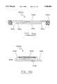
- FIG. 1is a cross-sectional view of a typical, prior art flip-chip structure.
- FIG. 2is a cross-sectional view of a prior art flip-chip assembly illustrating capillary action caused by liquid flux, resulting in the misalignment of a chip with respect to a substrate.
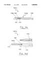
- FIG. 3is an exploded cross-sectional view of a flip-chip assembly, prior to soldering, according to a technique of the invention.
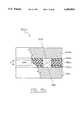
- FIG. 4is a perspective view of a plastic standoff element (preformed planar structure) employed in the technique of FIG. 3.
- FIG. 5is a perspective view of an alternate embodiment of a standoff element suitable to be employed in the technique of FIG. 3.
- the preformed planar structuremay alternately be referred to as an "interposer”.
- FIG. 6is an exploded cross-sectional view of a flip-chip assembly incorporating a preformed planar structure (interposer), according to the invention.
- FIG. 6ais a cross-sectional view of another embodiment of a preformed planar structure, similar to that shown in FIG. 6, according to the invention.
- FIG. 6bis a cross-sectional view of another embodiment of a preformed planar structure, similar to that shown in FIG. 6a, according to the invention.
- FIG. 6cis a cross-sectional view of an encapsulated semiconductor die assembled to a preformed planar structure, according to the invention.
- FIG. 7is a cutaway view of a preformed planar structure including a ring-shaped array of angled through holes, according to the invention.
- FIG. 7ais a top view of the preformed planar structure of FIG. 7.
- FIG. 7bis a top view of a preformed planar structure with a rectangular array of angled through holes, according to the invention.
- FIG. 8is a cross-sectional view of a semiconductor device assembly employing a preformed planar structure as a connection "pitch adapter", according to the invention.
- FIG. 8ais a cross-sectional view of a semiconductor device assembly employing a multi-layer preformed planar structure as a connection pitch adapter, according to the invention.
- FIG. 9ais a view of a semiconductor device assembly employing dissolvable preformed planar structures, according to the invention.
- FIG. 9bis a view of a the semiconductor device assembly of FIG. 9a, after dissolving the preformed planar structures.
- FIG. 10ais a view of a ring-shaped preformed planar structure, according to the invention.
- FIG. 10bis a view of a gapped ring-shaped preformed planar structure, according to the invention.
- FIG. 10cis a close-up top view of a portion of a leg of a kerfed ring-shaped preformed planar structure (interposer), according to the invention.
- FIG. 10dis a side view of the kerfed interposer of FIG. 10c.
- FIG. 10eis a close-up top view of a portion of a leg of another embodiment of a kerfed ring-shaped preformed planar structure (interposer), according to the invention.
- FIG. 10fis a side view of the kerfed interposer of FIG. 10e.
- FIG. 11ais a cross-sectional view of a semiconductor device assembly employing a preformed planar structure (interposer) with an embedded conductive trace and probe finger, according to the invention, before assembly.
- interposerpreformed planar structure
- FIG. 11bis a cross-sectional view of a semiconductor device assembly employing a preformed planar structure with an embedded conductive trace electrically connecting two different solder bump connections, according to the invention.
- FIG. 11cis a side view of a semiconductor device assembly employing a preformed planar structure (interposer) wherein embedded conductive traces exit the interposer and form conductive leads of the assembly, according to the invention.
- interposerpreformed planar structure
- FIG. 11dis a top view of a preformed planar structure (interposer) similar to that of FIG. 11c, wherein conductive leads embedded in the interposer are connected to an external "ribbon-cable" according to the invention.
- FIG. 12is a cross-sectional view of a semiconductor device assembly employing noble metal conductors embedded in a preformed planar structure to prevent electro-galvanic corrosion of dissimilar solder bump contacts, according to the invention.
- FIG. 13ais a cutaway side view of one embodiment of a stepped preformed planar structure, according to the invention.
- FIG. 13bis a cutaway side view of another embodiment of a stepped preformed planar structure, according to the invention.
- FIGS. 14a-dare side views of various embodiments of transparent, colored, clear, and translucent preformed planar structures (interposers) according to the invention.
- FIG. 15ais a side view of a flip-chip semiconductor device assembly, according to the invention.
- FIG. 15bis a side view of a multi-tier flip-chip semiconductor device assembly, according to the invention.
- FIG. 15cis a cutaway side view of a flip-chip semiconductor device assembly, according to the invention, before assembly.
- FIGS. 1 and 2illustrate a prior art technique of assembling flip-chips 10.
- the completed flip-chip structure 10includes one or more silicon chips 12 (two of such chips are illustrated) mounted in face-to-face relationship to a larger silicon chip or substrate 14 in the following manner.
- Solder balls (or pads) 16are formed on the face 12A of the chip 12
- solder balls (or pads) 18are formed on the face 14A of the substrate in corresponding positions (i.e., to align with the solder balls 16 of the chips).
- solder balls on either the chip 12 or on the substratemay simply be solderable metallized surfaces.
- balls (of dollops) of conductive epoxy or polymercould be used in lieu of solder balls. In the main hereinbelow, solder balls are discussed.
- Liquid flux 20(shown in FIG. 2 only) is applied to the face 14A of the substrate, prior to bringing the chips 12 in face-to-face relationship with the substrate 14.
- the chips 12are placed in face-to-face relationship by mechanical means, such as with a chuck (not illustrated), and the temperature of the chips and substrate is elevated sufficiently to cause the solder balls 16 on the face 12A of the chips 12 to "fuse" forming solder joints, with the corresponding solder balls 18 on the face 14A of the substrate 14.
- the liquid flux 20fills a gap 22 between the faces 12A of the chips 12 and the face 14A of the substrate 14, and also fills an area on the face 14A of the substrate 14 between the chips 12.
- Capillary action and/or surface tension created by the presence of the liquid flux 20causes the chips 12 to migrate to the center 24 of the substrate 14 during the soldering process, resulting in a lack of registration between the chips 12 and the substrate 14, and hence between the solder balls 16 and the corresponding solder balls 18, respectively.
- This tendency of the chips to become misaligned during solderingis augmented by any initial lack of planarity between the chips 12 and the substrate 14, and is extremely disadvantageous in the assembly of flip-chips.
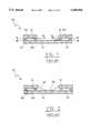
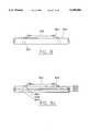
- FIG. 3illustrates a technique of assembling flip-chips 30.
- the flip-chip assembly 30includes one or more silicon chips 32 (two of such chips are illustrated) ultimately mounted in face-to-face relationship to a larger silicon chip or substrate 14 in the following manner.
- Solder balls 36are formed on the face 32A of the chip 32, and solder balls 38 are formed on the face 34A of the substrate 34 in corresponding positions.
- liquid fluxis not applied to the face 34A of the substrate 34, prior to soldering the chips 32 thereto.
- liquid fluxrequired to be applied to the faces 32A of the chips 32.
- a preformed planar structure 40Prior to soldering the chips 32 to the substrate 34, a preformed planar structure 40 (otherwise termed a “stamp” or “plastic standoff element”, and discussed in greater detail hereinafter), of similar planar dimension as the chip 32, is interposed between the chips 32 and the substrate 34.
- the planar structure 40is provided with through holes 42 in positions corresponding to the positions of the solder balls 26 and 38, respectively. Inasmuch as the solder balls 36 are typically located just within the perimeter of the chips 32, the through holes 42 would be located just within the perimeter of the planar structure 40.
- the planar structure 40Prior to soldering, the planar structure 40 is dipped (not illustrated) into a solution (bath) of liquid flux, such as rosin material, and is allowed to dry, as shown at 44. In this manner, the planar structure 40 receives selectively deposited rosin preferentially within the holes 42, in registration with the corresponding solder balls 32 and 34, and there will be very little, if any, flux on the planar surface of the preformed planar structure.
- the capillary action of liquid solutions in small holesdraws the bulk of the liquid flux material into the through holes 42, which are disposed in register with the solder balls, to effect successful solder bonding.
- the chips 32are more easily and accurately held in place by mechanical means, such as with a chuck (not illustrated) during soldering, resulting in increased throughput (yield) of flip-chips in the manufacturing process.
- the holes 42 in the planar structure 40assist in maintaining registration of the solder balls 36 and corresponding solder balls 38, respectively, and hence alignment of the chips 32 with respect to the substrate 34.
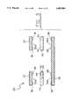
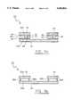
- FIG. 4shows, in further detail, the preformed planar structure 40 used in the technique of FIG. 3. References to FIG. 3 are made in the following paragraphs.
- the preformed planar structure 40includes a planar core 46 formed of a material such as thermosetting organic resin or non-organic material (e.g. aluminum sheet, alumina sheet, beryllium oxide sheet). Laminated to both opposing faces of the core 46 are planar layers (faces) 48 formed of thermoplastic (resin) or thermosetting "skin" which can be expected to soften significantly at the elevated temperatures employed for solder reflow in the flip-chip bonding process. This softening and consequent shrinking of the thermoplastic resin skin (and hence shrinkage of the overall planar structure) will allow and encourage the chips to draw or grow closer to the substrate in response to surface tension caused by the molten solder balls and surface tension of the skin itself.
- a materialsuch as thermosetting organic resin or non-organic material (e.g. aluminum sheet, alumina sheet, beryllium oxide sheet).
- faces 48formed of thermoplastic (resin) or thermosetting "skin” which can be expected to soften significantly at the elevated temperatures employed for solder re
- thermoplastic faces 48will re-solidify after soldering (upon reduction in temperature) and create a cushion for the faces 32A and 34A of the chips 32 and substrate 34, respectively. Simultaneously, the shrinkage of the planar structure 40, especially the thermoplastic faces 48 thereof, will have the effect of drawing the chips together as they cool off to room temperature after soldering. In this manner, the solder balls are mechanically kept in contact with the chips and substrate, respectively, as well as with each other.
- the core 46 of the preformed planar structureexhibits good thermal conductivity, and is formed of a rigid thermosetting organic resin or non-organic material, such as polyimide, polished alumina, polished sapphire, beryllium oxide, aluminum/or aluminum nitride.
- a suitable polyimideis available from CIBA-GEIGY Corporation, Santa Clara, Calif., in their Probimide (TM) 300 or 400 Series, or Selectilux (TM) HTR 3, microelectronic materials.
- the faces 48 of the preformed planar structure 40are formed of a thermoplastic material such as polyacetal, epoxides or polystyrene. It is advantageous that the preformed planar structure exhibit hermeticity and that it does not wick the liquid flux.
- the overall thickness of the preformed planar structure 40is on the order of 5-50 microns, preferably 30-30 microns, and the preformed planar structure acts as a physical barrier standoff between the chips and the substrate.
- a synergistic effectresults from the use of the preformed planar structure which effectively eliminates flux from the faces of the chips and substrate by selectively causing the flux to be deposited on the solder balls and corresponding solder balls, respectively.
- any adhesion of the planar structurenotably the "skin" thereto effects a mechanical connection of the solder balls and corresponding solder balls irrespective of soldering.
- Albeitthe adhesion and shrinkage become effective at the elevated temperature experienced during soldering. This satisfies the adage that, "good mechanical Joints lead to good solder joints".
- the preformed planar structure 40serves as a plastic standoff element to determine the size of the gap between the chips and the substrate.
- the relatively solid core 46 of the planar structure 40sets a relatively rigid lower limit on the amount that the chips can grow (draw) together to the substrate as the solder balls and corresponding solder balls melt and fuse together.
- the mechanical properties of the solder jointsremain somewhat indeterminate.
- the planar structure 40in the manufacturing process, flip-chip structures can be formed without the usual concerns about solder ball bond rigidity.
- the through holes 42form a generally cylindrical "mold" of predetermined dimension wherein the solder joints are formed.
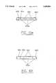
- FIG. 5is a perspective view of an alternate embodiment of a preformed planar structure, or standoff element 50, suitable to be employed in the technique of FIG. 3. References to FIG. 3 are made in the following paragraphs.
- the standoff element 50is similar to the standoff element 40 shown in FIG. 4. However, rather than having through holes 42 in alignment with the solder balls 32 and corresponding solder balls 34, the standoff element 50 may be provided with corner cutouts 52 in alignment with the solder balls 32 and corresponding solder balls 34, and is sufficiently sized so that the solder joints are formed just outside its perimeter. The surfaces of the corner cutouts 52 can be left relatively rough (as compared with the faces 58) in order that liquid flux 54 tends to adhere thereto (as opposed to draining off the faces 58).
- the liquid fluxis applied to the planar structure 50 by dipping the planar structure in a bath of liquid flux which is allowed to dry thereon. Under the elevated temperatures employed for solder bonding, the flux will be delivered to the solder balls 32 and to the corresponding solder balls 34.
- the advantages of the standoff element (preformed planar structure) 50are similar to those of the standoff element 40 with respect to forming a gap of predetermined dimension between the chip and the substrate, aiding in drawing together the chip and the substrate, mechanically drawing together the solder balls and the corresponding solder balls, requiring less flux to effect soldering and, to a lesser extent aiding in maintaining alignment of the chip and the substrate and alleviating the usual concerns about solder ball bond rigidity.
- the preformed planar (layered) structurecushions and draws and holds (upon re-solidifying) the chip and the substrate together in the flip-chip manufacturing process. This improves the mechanical integrity of the flip-chip assembly and increased the resistance thereof to loss of electrical contact between the solder balls. This is important in that the solder balls themselves serve as the mechanical point of attachment between the chip and the substrate. Chip (to substrate) draw together is controlled, and a permanent tension is created between the chip and substrate.
- the inventionsolves the problem of using too much flux and having the position of the chips change during bonding (soldering).
- the inventionallows the use of an absolute minimum of flux so subsequent cleaning of the flip-chip assembly is simplified.
- the coremay be formed of thermosetting organic resin, such as polyimide, or of non-organic material such as alumina, polished sapphire, beryllium oxide, aluminum nitride or aluminum.
- the planar faces of the preformed planar structuremay be formed of thermoplastic resin or thermosetting material, such as polyacetal, epoxide resin or polystyrene. Methods of mounting a chip (e.g., semiconductor die) to a substrate (e.g., another semiconductor die), using the preformed planar structure are discussed.
- the preformed planar structuresserve at least two purposes: (1) the through holes or cutouts allow for selective fluxing and ensure predictable mechanical characteristics of joints formed by solder balls, and (2) the preformed planar structure provides a prescribed standoff (separation) between the chip and the substrate, and also helps draw them together in intimate contact with the preformed planar structure.
- the preformed planar structureis often referred to as an "interposer", especially in those cases where it is literally interposed between a chip and a substrate.
- the substratecould be a printed circuit board, another chip or chips, or the like.
- the chipcould be a complete packaged semiconductor device.
- the preformed planar structures of commonly-owned parent U.S. Pat. Nos. 5,111,279 and 5,168,346generally disclose an interposer (preformed planar structure) for forming solder joints between a chip and a substrate having the same pitch, or spacing, of solder bumps. Generally, the through holes or cut outs extended perpendicularly through the preformed planar structure.
- one face of a preformed planar structureis provided with an array of holes disposed at one pitch (spacing) for aligning with the solder bumps of a chip
- the other face of the preformed planar structureis provided with an array of holes at another pitch for aligning with solder bumps on a substrate.
- Angled or bent through holes through the preformed planar structureextend from the one holes to the other holes, and may be partially or fully filled with a conductive material prior to assembling the chip to the substrate.
- a preformed planar structureis interposed between at least one die and an underlying substrate.
- the underlying substratebeing part of an external system, such as a printed circuit board).
- the preformed planar structureis provided with at least one through hole. At least one electrical connection is made from the at least one die, through the at least one through hole to connection points on the underlying substrate.
- the dieis flipped face-down onto a face of the preformed planar structure, and solder balls on the face of the die align with the through holes on the face of the preformed planar structure.
- Circuit elementsmay be formed on the face (obverse) or back (reverse) side of the die. Typically, the circuit elements would be formed on the face of the die.
- the (at least one) through holes in the preformed planar structureare pre-filled, or partially pre-filled, with conductive material, such as metal, solder, or conductive polymer or epoxy, such as silver-filled epoxy.
- conductive materialsuch as metal, solder, or conductive polymer or epoxy, such as silver-filled epoxy.
- the reverse (opposite the die) side of the preformed planar structureis provided with ball bumps, or the like, for making connections from external systems (via the underlying substrate) to the die.
- the preformed planar structureforms a significant part of the package body surrounding and/or supporting the die.
- the through holesare partially pre-filled with conductive material, and are then pre-fluxed for subsequent attachment of the die and formation of the ball bumps.
- the through holesare disposed at various angles through the preformed planar structure so that they have a first, relatively close spacing on the face of the preformed planar structure receiving the die (for making connections to an array of closely-spaced solder bumps on the face of the die), and have a second, relatively far-apart spacing on the face of the preformed planar structure making connection to external systems.
- the connection to external systemswould typically be achieved by means of a printed circuit board (PCB) which would have connection points disposed at a greater pitch than the solder bumps on the die.
- PCBprinted circuit board
- At least one dieis mounted to a preformed planar structure having at least one through hole. At least one connection to the die is made through the at least one through hole. Additional connections to the die are made on the side of the die facing away from the preformed planar structure, such as by wire bonding.
- the preformed planar structurehas a planar core and opposing planar faces.
- the coreis formed of thermosetting organic resin, such as polyimide, or non-organic material such as alumina, polished sapphire, beryllium oxide, aluminum or aluminum nitride.
- the planar faces of the preformed planar structureare formed of thermoplastic resin or thermosetting material, such as polyacetal, epoxy (epoxide resins) or polystyrene.
- FIG. 6shows (exploded) a die 602 flipped onto a face 604 of a preformed planar structure 606.
- the preformed planar structure 606is similar to the previously described structures (see, e.g., the structure described as 40, FIG. 3), but the through holes 608 (compare with through holes 42, FIG. 3) are at least partially filled with a conductive material 610.
- the conductive material 610is recessed below the die-side 604 of the preformed planar structure.
- conductive balls (raised conductive bumps) 612 disposed on the face 614 of the diewill partially enter the recesses 616 formed in the top surface 604 of the preformed planar structure 606.
- fluxcan be selectively applied to the preformed planar structure, depositing itself exclusively in the recesses, in a manner similar to that set forth with respect to the preformed planar structure 40 (FIG. 3) .
- the conductive material 610may be metal, which will fuse with the balls 612, which may be formed of solder. In this manner, a solder joint of predetermined mechanical structure is formed in the recess, similar to what has been described above with respect to FIGS. 3-5.
- the conductive materialmay be a conductive polymer
- the balls 612may also be formed of a conductive polymer, in which case there will be an adhesion between the balls 612 and the conductive material 610.
- the conductive material 610is not recessed below the surface 604 of the preformed planar structure, but is flush with same, as shown in FIG. 6a, or extends slightly above the surface of same, as shown in FIG. 6b.
- the conductive material 610may extend only partially to the opposite surface 618 of the preformed planar structure 606, as shown in FIG. 6, and the resulting recesses can be pre-fluxed in a manner similar to that described with respect to the preformed planar structure 40 (FIG. 3).
- the recesses formed by the partially-filled through holeswill allow self-registration of conductive balls (raised conductive bumps) 620 on the surface of an underlying substrate 622 to self-self align with the preformed planar structure (with die mounted thereto).
- the underlying substrateis, for example, a printed circuit board with wire traces (not shown), and electrically connects the die to external components or systems (not shown).
- solder balls 621may be formed on the bottom surface of the preformed planar structure.
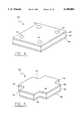
- the preformed planar structure 606is preferably larger than the die 602, and the die, once joined to the preformed planar structure, can be encapsulated with epoxy 624, or the like. In this manner, the preformed planar structure 606 forms part of a package body enclosing the die. The epoxy 624 forms the remainder of the package body.
- the preformed planar structure of FIG. 6cwould preferably be provided with solder balls such as those shown in FIG. 6 at 621.
- the preformed planar structure 606is preferably thicker than the previously described preformed planar structures (e.g., 40, 50, FIG. 3), and preferably will provide adequate structural support for the die, especially when used in the manner set forth with respect to FIG. 6c. Additionally, a thicker (e.g., than that of FIG. 3) preformed planar structure may be used as a "pitch adapter" for connecting conductive bumps (612) of the die, at a relatively fine pitch, to conductive bumps (620) of an underlying substrate at a relatively coarse pitch.
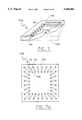
- FIG. 7shows a cutaway portion of a relatively thick preformed planar structure (interposer) 700 having one surface 702 upon which a die (not shown) will be mounted, and an opposite surface 704 which will be mounted to an underlying substrate (not shown). (The remaining outline of the preformed planar structure 700 is shown in dashed lines 700a.)
- the preformed planar structure 700is similar to that described with respect to FIGS.
- the through holes 710are arranged at a range of angles with respect to the surfaces 702,704, such that at least some of the openings (e.g., 716) of the through holes 710 in the bottom surface 704 are not directly under (i.e., are offset from) corresponding openings (e.g., 706) in the top surface 702 of the interposer 700.
- the through holeswere generally all disposed at ninety degrees ("normal") to the surfaces of the preformed planar structure, such that the bottom openings of the through holes were located generally directly beneath the corresponding top openings.
- the through holes 704can be made to exit the one surface 702 of the preformed planar structure 700 at one spacing ("pitch"), for example in a linear array matching a pattern of closely spaced conductive bumps arranged around the periphery of a die, and can be made to exit the other surface 704 of the preformed planar structure 700 at a different, larger pitch, for matching a pattern of conductive bumps (or pads) on an underlying substrate (e.g., PWB), which may be arranged in a rectangular array of rows and columns.
- PWBunderlying substrate
- FIG. 7ashows a top view of the preformed planar structure 700, and is illustrative of relatively close spacing of the top openings 706 of the through holes 710 as they exit the die-mounting face 702 of the preformed planar structure. Dashed lines indicate the angled trajectory of the through holes 710 through the preformed planar structure 700, ending in bottom openings 716 which are relatively more widely spaced than the top openings 706.
- FIG. 7bshows a top view of a similar preformed planar structure 700'.
- the preformed planar structure 700 of FIG. 7showed through holes 710 the top openings of which were arranged in rows
- the preformed planar structure 700'has through holes 710' with top openings 706' arranged in a rectangular array on a top (die mounting) surface 702 thereof.
- the through holes 710'generally "fan outward" as they pass through the preformed planar structure 700', ending in bottom (substrate-side) openings 716' which are generally wider spaced than the top side openings 706'.
- the through holes 710 or 710'are filled with conductive material (not shown) in one of three ways at each surface: (1) the conductive material is recessed below the surface (compare FIG. 6); (2) the conductive material is flush with the surface (compare FIG. 6a); (3) the conductive material extends out of the surface (compare FIG. 6b).
- Ball bumpsmay suitably be applied to the non-die side of the pitch-spreading interposer, and a die mounted thereto can be encapsulated as in FIG. 6c.
- the preformed planar structure of this inventioncan be advantageously applied to situations where it is desirable to package semiconductor dies and attach the packaged dies to underlying substrates having a rectangular array (rows and columns) or ring-shaped array (e.g., as in FIG. 7a) of connection points.
- the preformed planar structure (interposer) of this inventioncan also be advantageously applied to situation where it is necessary to accommodate less regular arrangements of connection points.
- a substratemight have connection points disposed in a zig-zag (or seemingly random) pattern to mate with corresponding solder bump contacts on a semiconductor die arranged in a linear configuration.
- the diecan be readily adapted, i.e., connected, to the substrate.
- the interposer of this inventioncan serve not only as a pitch spreader, but can also be advantageously employed as an adapter to join connection points (e.g., of a die and a substrate) having completely dissimilar patterns. It will be readily appreciated by one of ordinary skill in the art that many different types of connection point adaptations can be accommodated by the present invention.
- the printed circuit boardis provided with plated vias holes connecting wiring traces on the one (die) side of the board to the other (ball bump) side of the board. Additionally, there are traces on the bottom side of the board connecting the plated vias to the ball bumps.
- solder bumpse.g., a two-dimensional rectangular array of raised contacts.
- the printed circuit boardis provided with plated vias holes connecting wiring traces on the one (die) side of the board to the other (ball bump) side of the board. Additionally, there are traces on the bottom side of the board connecting the plated vias to the ball bumps.
- An inherent problem with the traces and ball bumps on the other (ball bump) side of the boardis that the plated vias are generally arranged around the periphery of the board, and must navigate through adjacent ball bumps, especially to connect to ball bumps located in central areas of the array. Consequently, the ball bumps must be arranged with rather wide spacing, to accommodate one or more (typically more) traces passing therebetween.
- the preformed planar structure (e.g., 700) of the present inventionthere is no need for traces on the bottom (away from the die) side of the package body.
- the bottom side of the preformed planar structuremay be provided with conductive ball bumps, for surface-mounting the packaged die to a printed circuit board (compare FIG. 6).
- the face of the preformed planar structure to which the die is attachedis provided with a thermoplastic layer, or the like (compare 40), which will have the effect of drawing the semiconductor die into intimate contact with the preformed planar structure.
- FIG. 8shows an alternate embodiment of the invention, wherein a die 800 is mounted to a face of the preformed planar structure 800, and is connected with bond wires 804 thereto.
- the preformed planar structuremay be similar to any of the preformed planar structures (606, 700) set forth hereinabove.
- the through holes 806can be formed at angles with respect to the faces of the preformed planar structure.
- FIG. 8ashows an example of such a multi-layer structure, similar to that shown in FIG. 8, except that three laminated layers 802a, 802b, and 802c form the preformed planar structure.
- through holescan be "stepped" (they can follow non-linear paths).
- a through hole consisting of three parts, 806a, 806b, and 806c,is shown extending through the three layers 802a, 802b, and 802c.
- the top-most portion 806a (nearest the die 800) of the through holeextends vertically (as depicted) through the top-most layer 802a of the preformed planar structure.
- a second portion 806b of the through holeextends horizontally through the second layer 802b.
- a bottom-most portion 806c of the through holeextends vertically through the bottom-most layer 802c of the preformed planar structure.
- the preformed planar structures (interposers) of commonly-owned parent U.S. Pat. Nos. 5,111,279 and 5,168,346generally disclose a "spacer” or “interposer” between a semiconductor die and another die or substrate.
- the preformed planar structure (40, 50)remains interposed between the chip(s) and the substrate, and may provide for entrapment of contaminants. Contaminants in a flip-chip structure (assembly) are generally undesirable, and may lead to device failure.
- a dissolvable preformed planar structurecan be formed similarly to other preformed planar structures described herein (especially those of FIGS. 3-5), and used to assemble a semiconductor die to a substrate in much the same manner as described hereinabove (e.g., with respect to FIG. 3).
- the preformed planar structureis dissolved with a suitable solvent, permitting more effective removal of contaminants trapped during the assembly process.
- FIG. 9ais a cross-sectional view of a flip-chip assembly, prior to soldering, similar to that of FIG. 3, but employing a dissolvable preformed planar structure 40'.
- the flip-chip assembly 30includes one or more silicon chips 32 (two shown) ultimately mounted in face-to-face relationship to a larger silicon chip or substrate 14.
- Solder balls 36are formed on the face 32A of each chip 32, and solder balls 38 are formed on the face 34A of the substrate 34 in corresponding positions.
- liquid fluxis not applied to the face 34A of the substrate 34, prior to soldering the chips 32 thereto.
- the preformed planar structure 40'is interposed between the chips 32 and the substrate 34.
- the preformed planar structure 40'is dipped (not shown) in liquid flux, so that it adheres within the bore of the through holes (or to the surface of the cutouts).
- This selective application of flux to the solder ballshas the same advantages as described hereinabove with respect to FIG. 3 and can be controlled in the same manner as described hereinabove.
- solder jointsform within the through holes (or cutouts), and the preformed planar structure is removed by exposing it to a suitable solvent.
- a suitable solventto remove any remaining contaminants.
- the preformed planar structure 40'can be made of a material which is soluble in the solvent used to remove the contaminants, permitting dissolution of the preformed planar structure 40' and removal of the contaminants in a single step.
- the solventmust be chosen in accordance to the particular material of which the interposer (preformed planar structure) is formed.
- a dissolvable preformed planar structureprovides all of the assembly advantages of the other preformed planar structures described hereinabove, and has the additional advantage that by removal (dissolution) of the preformed planar structure, any contaminants trapped during assembly can be very effectively eliminated.
- the interposers of FIGS. 6, 6a, 6b, 7, 7a or 7bcould readily be dissolved after the chip is connected to a substrate.
- a chipis mounted to an interposer such as that of FIGS. 6, 6a or 6b, then the interposer would be dissolved, leaving a chip with exaggerated raised contacts (e.g., 610) on the surface thereof, to later be mounted to a substrate.
- interposersof commonly-owned parent U.S. Pat. Nos. 5,111,279 and 5,168,346 are generally solid and unyielding, and therefore generally unable to conform to poorly planarized substrates such as printed circuit board substrates. (It is assumed that, typically, the die itself is relatively highly planar.) In such a case of mounting a die to a non-planar substrate surface, the interposer structure could actually "lever" the die away from the substrate, which would lead to less reliable solder bump attachment.
- the interposeris formed as a ring like structure, rather than as a solid volumetric structure such as has previously been described (e.g., 40).
- the various "legs" of the ringare relatively (to the volumetric solid) insubstantial and, hence, are able to skew (deform) themselves to accommodate surface irregularities on the surface of an underlying non-planar substrate.
- the interposeris formed as a ring-like structure with a gap for extra flexibility.
- the interposer structureis formed of polyimide, alumina, berylia, silicon, silicon dioxide, or the like. Materials of unusually high stiffness can be used, and the resulting interposer structure will still exhibit the necessary flexibility for non-planar substrates.
- the present inventionrecognizes (assumes) that bond pads (solder bumps) will generally be arranged in a linear array just inside the periphery of a die.
- a ring-like interposer structureis provided with a plurality of notches ("kerfs") so that it will exhibit the necessary flexibility for non-planar substrates.
- the kerfsare disposed between the locations of the through holes.
- the kerfsmay be disposed on the top and/or bottom surfaces of the ring-like interposer.
- FIG. 10ashows an embodiment of the ring-like interposer structure 1000a of the present invention formed in a narrow, solid (closed) ring 1002a. Because of the narrow legs of the ring shape 1002a, the interposer 1000a is capable of a certain amount of flexing to conform to an irregular surface. By flexing and conforming, the aforementioned "levering" of the die is reduced or eliminated. As stated hereinabove, the ring-like shape of the interposer assumes a similarly shaped ring-like array of solder bumps on a die and substrate between which the interposer will be assembled.
- the shape of the ring-like interposer 1000acan be readily adapted to any "outline"-shaped array of bond pads, e.g., triangular, circular, etc.. Through holes are omitted from this view, for illustrative clarity, but would be similar to the through holes of the preformed planar structure of FIG. 3. Additionally, the through holes could be pre-filled, as in FIGS. 6, 6a or 6b.
- FIG. 10bshows another embodiment of the ring-like interposer structure 1000b of the present invention.
- the interposer 1000bis formed as a ring-like structure 1002b with a gap 1004.
- the gap 1004the ring-like structure 1002b is an "open" ring, and the resultant interposer 1000b is even more compliant than the interposer 1000a of the previous embodiment.
- the outside dimension of the interposeris approximately equal to the outside dimension of the die to be attached, and is provided with through holes (not shown) aligned with solder balls on the die (not shown).
- the ring-like interposer structureis able to accommodate significant non-planarity of an underlying substrate without introducing significant levering effects associated with the solid interposer.
- the interposerdoes not serve to render the substrate more planar, but by better conforming to surface irregularities (non-planarities) of the substrate the interposer prevents "amplification” of (transmitting of) the non-planarity as "seen” by the die to be attached to the substrate.
- the ring-like interposer structures of the present inventionare of great advantage when used in conjunction with substrates which are not surfaces of conic projections.
- solid (versus ring-like) interposersespecially those of certain polymer materials, can accommodate the simple bend of the surface.
- a solid interposercannot accommodate the bending in the required three dimensions.
- the ring-like interposer (e.g., 1000a) of the present inventioncan be used, because the thin ring-like structure can be bent in three dimensions at the same time without the puckering distortions that would be observed in solid interposers.
- the ring-with-gap embodiment (1000b) described hereinabovecan follow even more significant surface irregularities and still accomplish the objectives of using an interposer structure between a chip and a substrate (e.g., establishing a prescribed standoff and causing the solder joints to be of predetermined mechanical characteristics).
- Through-holesare assumed to be present, but are not shown for the interposers of FIGS. 10a and 10b, in order to reduce illustrative clutter. Any of the techniques described hereinabove for the formation of interposers with through holes, solder bumps, liquid flux, etc., may be used in conjunction with a ring-shaped interposer.
- FIG. 10cshows an enlarged top view of a portion of a leg 1002 of a "kerfed" ring-shaped interposer, applicable to the ring-shaped interposers 1000a and 1000b described hereinabove with respect to FIGS. 10a and 10b, respectively.
- Through-holes 1010 through the leg 1002 of the interposerpermit alignment and controlled formation of solder bump contacts as described hereinabove.
- Slots or grooves (kerfs) 1012 cut (kerfed) in the top surface (as depicted) of the leg 1002facilitate bending of the leg 1002 in the vertical direction (out of the page, as depicted).
- FIG. 10dis a side view of the kerfed leg 1002 of FIG. 10c.
- the kerfs 1012will allow the interposer 1002 to bend in one axis, but will not significantly reduce the stiffness of the interposer in another axis (e.g., out of the page, as shown in FIG. 10d).
- the interposeris kerfed on one surface only, with the kerfs being disposed between the through holes.
- the leg 1002can be kerfed on both its upper and lower surfaces, as shown in FIGS. 10e and 10f, depicting top and side views, respectively.
- slots 1012aare also cut in the lower surface of the leg 1002.
- FIGS. 10e and 10fshow the upper slots 1012 and lower slots 1012a in an alternating pattern, but it will be readily apparent to one of ordinary skill in the art that the slots 1012 and 1012a may also be disposed opposite one another.
- the depth and placement of the slots 1012 and 1012acontrol the degree of flexibility of the leg 1002.
- increased flexibilitycomes at the cost of the overall strength of the interposer, i.e., deep slots can significantly weaken the interposer.
- the flexible interposerscan be dipped in liquid flux, etc.
- the flexible interposercan be made of a dissolvable material and removed after soldering as described hereinabove with respect to FIGS. 9a and 9b.
- the preformed planar structures (interposers) of commonly-owned, parent U.S. Pat. Nos. 5,111,279 and 5,168,346are provided with through holes or peripheral cutouts which allow the solder balls of a chip (located on one side of the interposer) to fuse with the solder balls of a substrate (located on the other side of the interposer).
- the through hole embodimentthe resulting solder joints are contained completely within the through holes, and lack controllability and observability. Any attempted probing of the solder joint connections, for whatever intended purpose, is similarly obviated by the fact that the solder joints are hidden within the preformed planar structure.
- a plurality of probe fingersare incorporated into the interposer.
- one end of a probe fingerextends to within the through hole, so that when the solder joint between the two solder bumps is made, the probe finger is completely immersed in solder and makes excellent electrical contact with the solder joint.
- the probe fingerextends laterally through the interposer, at least to the peripheral edge of the interposer, and preferably beyond the edge of the interposer. In this manner, making electrical contact to the solder bumps (and solder joints)is accomplished via the probe fingers integral with the interposer.
- FIG. 11ais a cross-sectional view of a portion of an embodiment of an interposer with integral probe fingers.
- An assembly 1100 of a die 1110 to a substrate 1130includes an interposer 1120 with a probe finger 1125.
- the die 1110has a solder ball contact 1140a disposed on a lower face 1110a thereof.
- the lower face 1110ais positioned above an upper face 1120a of the interposer 1120 such that the solder ball contact 1140a extends into a through hole 1150 in the interposer.
- the substrate 1130has a matching solder ball contact 1140b disposed on a surface 1130a thereof.
- the surface 1130a of the substrate 1130is positioned below a lower face 1120b of the interposer, such that the solder ball contact 1140b extends into the opposite end of the through hole 1150.
- a conductive lead 1125 within the interposer 1120extends into the through hole 1150 to form a probe finger 1125a.
- the assembly 1100is shown prior to reflow soldering. After reflow soldering, the two solder ball contacts 1140a and 1140b will fuse into a single solder joint structure, electrically connecting the die to the substrate. Moreover, the portion of the probe finger extending into the through hole in which the solder joint is formed will be in intimate mechanical and electrical connection with the resulting solder joint. Although only one probe finger is shown, any number of probe fingers can be extended in similar fashion into any number of respective through holes in any of the interposers described hereinabove or hereinbelow.
- solder bump contactprovides for several novel connection schemes.
- selected solder bumpscan be connected to one another, without increasing the complexity of either of the solder bump substrates. This permits some increase in complexity of the total circuit without significantly increasing the design or construction complexity of the semiconductor die.
- FIG. 11bSuch an arrangement is depicted in FIG. 11b, wherein an assembly 1100a similar to that shown as 1100 in FIG. 11a has two solder bump contacts 1142a and 1142b joined by a conductive lead 1125 within the interposer 1120.
- the die 1110is positioned with its lower face 1110a above the upper face 1120a of the interposer and the substrate is positioned with its upper face 1130a under the lower face 1120b of the interposer.
- the solder bump contacts 1142a and 1142b in through holes 1150a and 1150b, respectively,are shown after reflow soldering.
- the solder bump contactscapture and are electrically connected by the conductive lead 1125 which extends into the through holes 1150a and 1150b. In this case (i.e., for the purpose of connecting two solder joints together), it is not necessary that the probe finger extend to without the peripheral edge of the interposer, although that may be desired and implemented.
- a die and a substrateare of approximately the same size (e.g., two flip-chipped dies)
- it is very difficult, using conventional means, to join them together into any useful configurationbecause there is no room to make conventional (e.g., wire bond) electrical contact from the flipped-together dies to a package or circuit board.
- the use of a traced interposer with the probe fingers extended out to external leads or contactssolves this problem.
- Two diesare joined face-to-face with a traced interposer disposed between the two dies.
- the traces of the interposerextend outward from the solder bump area, for connecting the two flip-chipped dies to another substrate.
- interposer finger tracescan facilitate face-to-face (flip-chipped) connections between dies of virtually any relative sizes. It will further be appreciated that it is possible for the interposer finger traces to extend out from the edges of the die stack as conductive leads or contacts to become part of any of a large variety of packages and substrates, including: printed circuit boards, plastic packages, and M-Quad packages, to name but a few examples.
- FIG. 11cillustrates the case wherein two similar-size dies 1170a and 1170b are flip-chip assembled with a "traced" interposer (e.g., 1120, FIGS. 11a and 11b) disposed between them to form an assembly 1155.
- the traces within the interposer(not shown, compare FIG. 11a) are extended outside of the interposer to form leads 1180 by which the assembly 1155 can be mounted and electrically connected to a substrate 1160.
- a single interposercan be sized to extend across several dies, and need not be restricted to assemblies of two dies, or a die and a substrate. Since the interposer can extend across the area of several dies and/or substrates, evidently a substantial improvement in circuit density can be realized, with the associated aforementioned benefits of the use of the present inventive techniques. It should be noted that the interposer technology of the present invention is completely compatible with conventional printed circuit board manufacturing technology.
- interposersincluding multiple layers of traces between layers of insulating material. Assuming adequate dielectric characteristics of the insulating layers, it is possible to create wiring structures in the interposer which cross each other without electrically shorting. Also, in a manner similar to that used in multi-layer printed circuit boards, the multiple layers of traces can be interconnected (e.g., by conductive vias), as desired.
- the probe fingerscan become part of a structure which can be used to test the die functionally.
- a plurality of traces exiting the interposercan be connected to a test system, for testing the die in ways otherwise not possible via the substrate, for example, by providing access to every solder bump contact of the die. Such an arrangement is shown in FIG. 11d.
- FIG. 11dshows an assembly 1185 including an interposer 1190 to which at least one die (not shown) is mounted.
- Conductive traces 1194are disposed within the interposer 1190 (compare FIG. 11a) to respective connection points 1192 (e.g., similar to probe fingers 1125a of FIG. 11a).
- a ribbon cable 1195, or other suitable interconnection meansis electrically connected to the traces 1194, where they exit the peripheral edge of the interposer, thereby forming an electrical interface for external test equipment (not shown).
- the probe fingerscan be made to create separate interconnections (e.g., via a cable similar to 1195, or other suitable interconnection means) between two-or-more interposer structures (e.g., 1190), thereby permitting increased wiring complexity without increasing the complexity of either the die or the substrate.
- the probe finger traces exiting two or more interposerscan be connected to one another, and in some cases not connected to an underlying substrate at all.
- the "traced" interposers of this inventionmay provide electrical contact with the solder bumps on a facing die, if the die and substrate are placed under moderate pressure to force them together, even before the solder bumps are melted together. (This assumes, of course, that the through holes in the interposer are sized to permit the solder ball on the die to contact the probe finger.) This feature would permit preliminary testing of the die and substrate prior to final assembly (i.e., prior to heating to fuse the solder balls to one another).
- interposers of the present inventionare not required to be, but preferably are, mechanically strong enough to support the mounting of a facing die, or of a die and a substrate, to another major assembly, without other mechanical reinforcement.
- the material of the interposeris chosen to give the required mechanical properties.
- an interposercan be made of a single insulating and a single conducting material, benefits can be realized from the use of several different materials which are used as a series of layers to create the interposer.
- Adhesive layerse.g., contact adhesive, thermoplastic, or a thermosetting resin material can be applied to the faces of the interposer. These adhesive layers can be made to adhere strongly to a die, to a substrate material, or even to a PCB. The adhesive layer causes the die (or substrate) to grip the interposer firmly, providing additional mechanical stability.
- the adhesivecan also be used to keep the substrate/interposer/die stack under compression, which has the benefit of holding together solder bumps which might otherwise be mechanically weakened.
- Solder ballsare structures which are used to electrically connect a circuit board or other substrate to a semiconductor chip. These bumps are created in a number of ways, including: electron beam evaporation, high vacuum sputtering, and electroplating. In each process there are variations which make it difficult to maintain the exact composition of the deposited material from run-to-run. As a result, there can be significant differences in the composition of solder bumps on different substrates, even though they may have been formed by a similar process.
- Solder bumpsare typically fabricated from a variety of metals and their associated alloys. Typical of these metals are: lead, tin and zinc. Unless the solder bump structures on both the substrate and the chip are of exactly the same composition, electro-galvanic corrosion of the resulting solder joints can occur. The subject of electro-galvanic corrosion is discussed, in another context, in U.S. Pat. No. 4,478,915, incorporated by reference herein.
- an inert metal film structureis provided in the interposer and physically separates the dissimilar alloys of dissimilar solder bumps, and largely inhibits electrogalvanic corrosion processes that would otherwise be associated with solder joints formed by mixed (dissimilar) solder bumps.
- a thin film (foil) of a noble (inert to galvanic corrosion) metalis incorporated into the holes of the interposer to galvanically isolate the bumps of the chip from those of the substrate. Electrical conductivity between the bumps of the chip and the substrate is maintained by the conductivity of the noble metal.
- FIG. 12is a cross-sectional view of an interposer having a noble metal foil disposed in a through hole (one of many shown) to galvanically isolate the material of the die ball bump from the material of the substrate ball bump, while permitting effective electrical connection between the two ball bumps.
- An assembly 1200 of die/interposer/substrateis illustrated at a stage immediately prior to reflow soldering.
- the semiconductor device assembly 1200is formed of a semiconductor die 1210, an interposer (preformed planar structure) 1220, and a substrate 1230.
- a solder bump contact 1240ais disposed on a bottom surface 1210a of the semiconductor die 1210.
- a mating solder bump contact 1240bis disposed on a top surface 1230a of the substrate 1230.
- a through hole 1250extends through the interposer from its top surface 1220a to its bottom surface 1220b.
- An inert metal film 1225e.g., gold
- the bottom surface 1210a of the semiconductor die 1210is positioned in face-to-face alignment with the top surface 1220a of the interposer, such that the solder bump 1240a on the die 1210 extends into the top portion 1250a of the through hole 1250 towards the noble metal film 1225.
- the top surface 1230a of the substrate 1230is positioned in face-to-face alignment with the bottom surface 1220b of the interposer, such that the solder bump 1240b on the substrate 1230 extends into the bottom portion 1250b of the through hole 1250 towards the noble metal film 1225.
- the two solder bump contacts 1240a and 1240bWhen heat is ultimately applied to reflow the two solder bump contacts 1240a and 1240b, they will melt and bond to their respective sides of the metal film 1225. Because of the metal film 1225, the two solder bump contacts 1240a and 1240b can not come into direct (physical or chemical) contact with one another, but electrical conductivity therebetween is provided by virtue of the electrical conductivity of the noble metal film 1225. As a result, an electrical and mechanical bond is formed between the solder bump contact 1240a and 1240b without a chemical bond which could cause electrogalvanic corrosion.
- the noble metal film 1225is in electrical contact with the two solder bumps, it could readily be extended to outside the peripheral edge of the interposer in the manner of the probe fingers and traces (see FIGS. 11c and 11d) to provide external access to the solder bump contacts 1240a and 1240b via the interposer, or could be extended within the interposer structure to form electrical connections with other solder bumps (see FIG. 11b).
- the only significant difference between the arrangement of FIG. 12 and those of FIGS. 11a and 11bis that the noble metal film 1225 physically separates the solder bumps 1240a and 1240b after reflow, while the probe finger 1125a (FIG. 11a) permits the solder bumps (1140a and 1140b) to flow around the end of the probe finger and mix after reflow.
- the preformed planar structures (interposers) of commonly-owned U.S. Pat. Nos. 5,111,279 and 5,168,346are provided with through holes or peripheral cutouts which allow the solder balls of a chip (located on one side of the interposer) to fuse with the solder balls of a substrate (located on the other side of the interposer).
- the preformed planar structureis disposed entirely between the chip and the substrate.
- the interposeris placed on the substrate, and the chip is placed on the interposer.
- the through holes (or peripheral cutouts)provide some self-alignment of the die to the substrate, the process still requires accurate placement of the die.
- an interposerwhich has a cavity in its top surface, into which the die is placed.
- the cavityhas tapering side walls to facilitate placement of the die into the interposer cavity.
- an interposermust be larger than the die, since the cavity is approximately the size of the die.
- the interposermay be formed as an integral unit (both portions formed as one piece), or the die-encompassing portion can be formed separately and joined to the interposed portion. In the latter case, preferably, indexing keys are formed on the joining faces of the two portions to ensure that they are correctly assembled to one another. The two portions are joined with a suitable adhesive or by ultrasonic bonding.
- FIG. 13ashows a portion of a semiconductor device assembly 1300 using a one-piece stepped interposer 1302.
- the interposer 1302has a cavity 1310 extending into its upper surface 1302a.
- the cavity 1310is sized and shaped to receive and align a semiconductor die 1320.
- Through holes 1330extend from the cavity (underneath the die 1320) through the bottom surface 1302b of the interposer, to provide further alignment of the die 1320 (by its solder bump contacts, not shown) and controlled formation of solder bump electrical connections.
- a dieis placed in the cavity of the interposer, and both are assembled to a substrate.
- the interposed portion of the interposeri.e., the portion underneath the die
- the interposercan function as a pitch spreader/adaptor (compare FIGS. 7, 7a, 7b, 8, 8a)
- the interposermay be dissolvable (compare FIGS. 9a, 9b)
- the interposercan be formed as a ring-like structure (compare FIGS. 10a-f, in which case a portion of the cavity would extend completely through the interposer), and the interposer can be provided with probe fingers (compare FIGS. 11a-d) or anti-galvanic foils (compare FIG. 12).
- the interposercan also be designed to accommodate more than one semiconductor die, as shown in FIG. 13b.
- FIG. 13bis a cutaway view of a portion of an arrangement 1300a using a two-piece stepped interposer designed to accommodate two semiconductor dies.
- the interposeris formed of a planar base portion 1304 and a top portion 1306.
- the top portion 1306has tapered openings 1310a and 1310b sized and shaped to receive and align semiconductor dies 1320a and 1320b, respectively.
- the top portion 1306is assembled to a top surface 1304b of the base portion 1304 such that when placed in the openings 1310a and 1310b, the dies 1320a and 1320b, respectively, rest on the top surface 1304b of the base portion.
- Through holes 1330 and 1330a under the dies 1320a and 1320bextend through the base portion 1304 to its bottom surface 1304a. Solder bump contacts on the dies (not shown) extend into these holes 1330 and 1330a to form electrical connections with mating contacts on a substrate (not shown) to which the arrangement 1300a is ultimately assembled.
- interposersof commonly-owned parent U.S. Pat. Nos. 5,111,279 and 5,168,346 generally disclose an interposer aligning a die in the x, y and z axes above a substrate.
- an element other than a semiconductor die (chip)can be x-y-z aligned above a die (or substrate) in the same or similar manner.
- an optical elementsuch as a lens or a window
- condensationmay form on an inner surface of the (optical) element.
- a clear (transparent) interposer(preformed planar structure) is disposed in and fills a space between a die and an element disposed above the die.
- the interposermay be clear, or it may be colored. If colored, the interposer may exhibit the additional functionality of a color filter, such as for camera applications. Where image coherence is not required, as in a UV-erasable EPROM application, a translucent interposer may be used to great advantage.
- the interposermay have certain optical characteristics, such as:
- the interposercan be provided with embedded conductors terminating on the die-facing of the interposer and extending to an external surface of the interposer. In this manner, electrical connections to the die can be made through the interposer.
- the interposermay have its die-facing surface formed with indentations or through holes (or cutouts) arranged in a pattern matching elevated features (e.g., solder balls or other "relief” features) on the die, for ensuring precise x-y alignment with the die.
- elevated featurese.g., solder balls or other "relief” features
- the interposermay have its element-facing surface formed with a lip, or the like, for ensuring precise x-y alignment with one or more edges of the element.
- the surface of the interposer facing away from the diecan be molded as a lens, or can be formed with integral binary optics.
- Examples of materials for forming a clear or translucent interposerinclude: quartz, silica, polyvinylchloride (pvc), polyvinylcarbonates, and lucite.
- FIG. 14ais a cross-sectional view of an arrangement 1400a of a semiconductor die 1410a and a light transmissive window 1430a, separated by a substantially clear interposer 1420a.
- the window 1430ais built into a semiconductor device package 1440a and is, for example, a quartz window in a ceramic package for an EPROM.
- the interposer 1420ais "registered" to the semiconductor die by means of "lips" 1421a on the interposer 1420a which capture the edges of the die 1410a (compare the interposer with cavity of FIG. 13a)
- the interposercompletely fills the gap between the window 1430a and the die 1410a, thereby preventing the formation of condensation therein. If image coherence is not required through the interposer (e.g., as in a UV-erasable EPROM application), then the interposer can be translucent. Otherwise, the interposer should be transparent.
- FIG. 14bis a cross-sectional view of portion of a semiconductor device assembly 1400b including a lens 1430b.
- a clear or colored transparent interposer 1420bis used to accurately position an optical element 1430b (lens shown) relative to a semiconductor die 1410b.
- the interposer 1420bhas a planar section 1422b and a raised section 1421b (compare the interposer with cavity of FIG. 13a).
- the raised section 1421bcaptures and positions the optical element 1430b relative to the die 1410b.
- the planar section 1422bis clear and permits transmission of a coherent image therethrough.
- the planar section 1422bserves as a color filter for e.g., a camera application.
- planar section 1422bcan be omitted, leaving only the raised section 1421b in a ring-shaped configuration (similar to that described hereinabove with respect to FIGS. 10a-f).
- the ring-shaped interposerit may not be necessary (or even desirable) to use a clear or translucent material, since the interposer could be used as a light blocking wall between an optically sensitive area and a logic area of the die 1410b.
- FIG. 14cillustrates another use of a clear or translucent interposer.
- a semiconductor die 1410chas an optically sensitive area 1440 and a logic area 1450.
- semiconductor devicesare generally light sensitive, and in order to prevent mis-operation of logic elements (e.g., 1450), it is often necessary to shield them from exposure to light.
- a transparent or translucent interposer 1420c with a darkened (light blocking) area 1460is used to shield the logic 1450 from extraneous exposure to light.
- the non-light-blocking area of the interposercould be a colored transparent material to act as a colored filter, or a clear in an application which does not require color selectivity.
- Other applications which do not require image coherence through the interposer 1420ccan make use of a translucent material.
- the surface of the interposer 1420ccan also be given other optical characteristics, such as binary optic features 1430c formed on the surface of the interposer. (In order for this to be useful, the interposer must be made of a clear or colored substantially transparent material.
- interposers 1420b and 1420c described with respect to FIGS. 14b and 14c, respectively,can be aligned to the semiconductor die by means of indentations or raised features (not shown) to mate with corresponding raised features (e.g., solder bumps) or indentations, respectively, on the semiconductor die.
- FIG. 14dillustrates a semiconductor device assembly 1400d which combines the clear/colored/translucent interposers with the traced interposer techniques described hereinabove with respect to FIGS. 11a-d.
- an optically sensitive semiconductor die 1410dhas one or more solder bump contacts 1480 disposed on the top surface thereof.
- a clear, colored, or translucent interposer 1420dis aligned over the semiconductor die 1410d by means of one or more indentations 1490 in the interposer which mate with the one or more solder bumps 1480.
- conductive traces 1470extends into the indentations and, after reflow soldering, make contact with the solder bump contacts 1480.
- the tracescan be used to connect to other solder bumps, to connect to (or form) pins of a package body, etc.
- interposersof commonly-owned parent U.S. Pat. Nos. 5,111,279 and 5,168,346 and method of assembling flip-chip type assemblies contemplates, for example, mounting two dies to a substrate (see e.g., FIG. 3).
- the use interposerscan also be extended to more elaborate assemblies of chips.
- integrated circuit diesare diced (cut apart, or singulated) from a semiconductor wafer and are assembled into integrated circuit packages which have pins, leads, solder (ball) bumps, or conductive pads by which electrical connections may be made from external systems to the integrated circuit chip. These packages are then typically applied to circuit board assemblies comprising systems of interconnected integrated circuit chips.
- flip-chip arrangementsfacilitates high-density, high-performance packaging.
- Examples of various prior art "flip-chip” constructionsare found in U.S. Pat. Nos. 3,388,301; 4,545,610; 4,190,855; 4,811,082; 4,926,241; 5,039,628; 4,970,575; 3,871,014; and in Japanese Patent Numbers 61-142750; 61-145838; 57-210638; and in "Wafer-Chip Assembly for Large-Scale Integration", IEEE Trans. Elec. Dev., Vol. ED-15, No. 9 Sep. 1968.
- flip-chip assembliesare formed using a preformed planar structure interposed between the chip(s) and the substrate.
- Thisincludes chip-on-chip, chips-on-chip, small die on large die, more than one small die on a larger die or substrate, "brickwork” and multi-tier arrangements.
- the preformed planar structuremay have either through holes or peripheral cutouts. Unless otherwise specified, the terms "chip”, “die” and substrate are generally used interchangeably.
- Chip-on-chip assemblieshave been described hereinabove, and can use any of the different types of interposers. Some arrangements have been described as assemblies of a semiconductor die to a substrate with an interposer (preformed planar structure) between, but it will be readily appreciated by one of ordinary skill in the art that a semiconductor die may be employed as a substrate, thereby effectively forming multi-chip assemblies. In particular, FIG. 11c described a face-to-face flip-chip assembly with an intervening interposer. Conductive traces embedded in the interposer were used as "pins" of the flip-chip assembly for further assembly to another chip or substrate.
- FIG. 15ashows a small-die-on-large-die flip chip arrangement 1500a, wherein a large die 1510a is used as a substrate.
- An interposer 1520asuch as those described hereinabove is disposed between the large die 1510a and a smaller die 1530a. In this case, the interposer 1520 is approximately the same size as the smaller die.
- the interposer 1520acan be solid (rectangular) or ring-shaped (see FIG. 10a-f), and may have embedded conductive traces (see FIGS. 11a-d, 12).
- FIG. 15bshows a multi-tier flip-chip arrangement 1500b, with interposers disposed between each of the "tiers".
- Two "base-level” dies 1510bare bridged by a second-level die 1530b.
- An interposer 1520bseparates the base-level dies 1510b and the second-level die 1530b.
- a pair of third-level dies 1531bare "flipped" on the second-level die 1530b by means of a pair of interposers 1521b, thereby forming a three-tier flip-chip structure with all advantages described hereinabove with respect to interposers in semiconductor device assemblies.
- any of the other features of interposer described hereinabovecan be employed in the flip-chip configuration, e.g., the interposers can be either solid or ring-shaped, and can have embedded conductors.
- liquid fluxis applied to the preformed planar structure in order that the flux is selectively applied to the solder balls (pads) on the chip(s) and the substrate.
- the preformed planar structurehas a planar core and opposing planar faces.
- the coreis formed of thermosetting organic resin, such as polyimide, or non-organic material such as alumina, polished sapphire, beryllium oxide, aluminum or aluminum nitride.
- the planar faces of the preformed planar structureare formed of thermoplastic resin or thermosetting material, such as polyacetal, epoxy (epoxide resins) or polystyrene.
- the preformed planar structurehas a thickness of 5-50 microns, preferably on the order of 20-30 microns.
- FIG. 15cis a cutaway view of an assembly of two semiconductor dies 1510c and 1530c separated by an interposer 1520c.
- the first semiconductor die 1510chas a solder bump contact 1560 disposed on a surface thereof.
- the second semiconductor die 1530chas a matching solder bump contact 1550 disposed on a surface thereof.
- the two dies 1510c and 1530care arranged in a face to face configuration such that the two solder bump contacts 1560 and 1550 are aligned.
- the interposer 1520cis disposed between the two dies 1510c and 1530c such that the solder bump contacts 1560 and 1550 extend into opposite ends of a through hole 1540 in the interposer.
- Upper and lower faces 1524c and 1522c of the interposer 1520care made of a thermoplastic resin or thermosetting material, such as those described above. Upon application of heat, the faces 1522c and 1524c of the interposer 1520c form adhesive bonds with the two dies 1530c and 1510c, respectively. At the same time, the two solder bump contacts 1550 and 1560 melt and fuse to form an electrical connection between the dies 1510c and 1530c.
- the interposer 1520chas a thickness "d" between 5 and 50 microns, preferably 20-30 microns.
Landscapes
- Engineering & Computer Science (AREA)
- Microelectronics & Electronic Packaging (AREA)
- Computer Hardware Design (AREA)
- Power Engineering (AREA)
- Manufacturing & Machinery (AREA)
- Physics & Mathematics (AREA)
- General Physics & Mathematics (AREA)
- Condensed Matter Physics & Semiconductors (AREA)
- Wire Bonding (AREA)
- Electric Connection Of Electric Components To Printed Circuits (AREA)
Abstract
Description
Claims (13)
Priority Applications (3)
| Application Number | Priority Date | Filing Date | Title |
|---|---|---|---|
| US08/106,157US5489804A (en) | 1989-08-28 | 1993-08-12 | Flexible preformed planar structures for interposing between a chip and a substrate |
| US08/260,078US5468681A (en) | 1989-08-28 | 1994-06-15 | Process for interconnecting conductive substrates using an interposer having conductive plastic filled vias |
| US08/470,945US5821624A (en) | 1989-08-28 | 1995-06-05 | Semiconductor device assembly techniques using preformed planar structures |
Applications Claiming Priority (5)
| Application Number | Priority Date | Filing Date | Title |
|---|---|---|---|
| US40057289A | 1989-08-28 | 1989-08-28 | |
| US07/576,182US5111279A (en) | 1989-08-28 | 1990-08-30 | Apparatus for isolation of flux materials in "flip-chip" manufacturing |
| US07/775,009US5168346A (en) | 1989-08-28 | 1991-10-11 | Method and apparatus for isolation of flux materials in flip-chip manufacturing |
| US07/981,096US5299730A (en) | 1989-08-28 | 1992-11-24 | Method and apparatus for isolation of flux materials in flip-chip manufacturing |
| US08/106,157US5489804A (en) | 1989-08-28 | 1993-08-12 | Flexible preformed planar structures for interposing between a chip and a substrate |
Related Parent Applications (1)
| Application Number | Title | Priority Date | Filing Date |
|---|---|---|---|
| US07/981,096Continuation-In-PartUS5299730A (en) | 1989-08-28 | 1992-11-24 | Method and apparatus for isolation of flux materials in flip-chip manufacturing |
Related Child Applications (1)
| Application Number | Title | Priority Date | Filing Date |
|---|---|---|---|
| US08/260,078Continuation-In-PartUS5468681A (en) | 1989-08-28 | 1994-06-15 | Process for interconnecting conductive substrates using an interposer having conductive plastic filled vias |
Publications (1)
| Publication Number | Publication Date |
|---|---|
| US5489804Atrue US5489804A (en) | 1996-02-06 |
Family
ID=27503449
Family Applications (1)
| Application Number | Title | Priority Date | Filing Date |
|---|---|---|---|
| US08/106,157Expired - LifetimeUS5489804A (en) | 1989-08-28 | 1993-08-12 | Flexible preformed planar structures for interposing between a chip and a substrate |
Country Status (1)
| Country | Link |
|---|---|
| US (1) | US5489804A (en) |
Cited By (149)
| Publication number | Priority date | Publication date | Assignee | Title |
|---|---|---|---|---|
| DE19702014A1 (en)* | 1996-10-14 | 1998-04-16 | Fraunhofer Ges Forschung | Chip module and method for producing a chip module |
| US5753536A (en)* | 1994-08-29 | 1998-05-19 | Matsushita Electric Industrial Co., Ltd. | Semiconductor device and associated fabrication method |
| US5770889A (en)* | 1995-12-29 | 1998-06-23 | Lsi Logic Corporation | Systems having advanced pre-formed planar structures |
| US5817542A (en)* | 1996-03-29 | 1998-10-06 | Matsushita Electric Industrial Co., Ltd. | Method for bonding electronic components |
| US5831788A (en)* | 1997-06-27 | 1998-11-03 | Quantum Corporation | Circuit connector |
| US5834335A (en)* | 1995-09-28 | 1998-11-10 | Texas Instruments Incorporated | Non-metallurgical connection between an integrated circuit and a circuit board or another integrated circuit |
| US5838519A (en)* | 1997-03-17 | 1998-11-17 | Kabushiki Kaisha Toshiba | Printed circuit board, magnetic disk apparatus with the printed circuit board, and method for connecting the printed circuit board |
| US5863815A (en)* | 1997-02-25 | 1999-01-26 | Oki Electric Industry Co., Ltd. | Method of manufacturing semiconductor device |
| EP0921716A1 (en)* | 1997-12-04 | 1999-06-09 | Ford Global Technologies, Inc. | Reinforced solder joints for printed circuit boards |
| US5925930A (en)* | 1996-05-21 | 1999-07-20 | Micron Technology, Inc. | IC contacts with palladium layer and flexible conductive epoxy bumps |
| US5929520A (en)* | 1998-03-10 | 1999-07-27 | General Electric Company | Circuit with small package for mosfets |
| US6040630A (en)* | 1998-04-13 | 2000-03-21 | Harris Corporation | Integrated circuit package for flip chip with alignment preform feature and method of forming same |
| US6093971A (en)* | 1996-10-14 | 2000-07-25 | Fraunhofer-Gesellschaft Zur Forderung Der Angewandten Forschung E.V. | Chip module with conductor paths on the chip bonding side of a chip carrier |
| EP1019989A4 (en)* | 1997-07-16 | 2001-07-25 | Gen Dynamics Inf Systems Inc | Interposers for land grid arrays |
| US20010021541A1 (en)* | 1999-06-28 | 2001-09-13 | Salman Akram | Wafer-level package and methods of fabricating |
| US6316830B1 (en) | 1998-12-17 | 2001-11-13 | Charles Wen Chyang Lin | Bumpless flip chip assembly with strips and via-fill |
| US6319751B1 (en)* | 1998-12-17 | 2001-11-20 | Charles Wen Chyang Lin | Bumpless flip chip assembly with solder via |
| US6350386B1 (en) | 2000-09-20 | 2002-02-26 | Charles W. C. Lin | Method of making a support circuit with a tapered through-hole for a semiconductor chip assembly |
| US6350633B1 (en) | 2000-08-22 | 2002-02-26 | Charles W. C. Lin | Semiconductor chip assembly with simultaneously electroplated contact terminal and connection joint |
| US6350632B1 (en) | 2000-09-20 | 2002-02-26 | Charles W. C. Lin | Semiconductor chip assembly with ball bond connection joint |
| US6357864B1 (en) | 1999-12-16 | 2002-03-19 | Lexmark International, Inc. | Tab circuit design for simplified use with hot bar soldering technique |
| US6402970B1 (en) | 2000-08-22 | 2002-06-11 | Charles W. C. Lin | Method of making a support circuit for a semiconductor chip assembly |
| US6403460B1 (en) | 2000-08-22 | 2002-06-11 | Charles W. C. Lin | Method of making a semiconductor chip assembly |
| US6403400B2 (en) | 1998-12-17 | 2002-06-11 | Charles Wen Chyang Lin | Bumpless flip chip assembly with strips-in-via and plating |
| US6406939B1 (en) | 1998-05-02 | 2002-06-18 | Charles W. C. Lin | Flip chip assembly with via interconnection |
| US20020078401A1 (en)* | 2000-12-15 | 2002-06-20 | Fry Michael Andrew | Test coverage analysis system |
| US20020076854A1 (en)* | 2000-12-15 | 2002-06-20 | Pierce John L. | System, method and apparatus for constructing a semiconductor wafer-interposer using B-Stage laminates |
| US6417686B1 (en) | 1996-11-14 | 2002-07-09 | Si Diamond Technology, Inc. | Display panel test device |
| US20020097063A1 (en)* | 1999-11-16 | 2002-07-25 | Kline Jerry D. | Wafer level interposer |
| US6429516B1 (en)* | 1997-02-28 | 2002-08-06 | Fujitsu, Limited | Structure for mounting a bare chip using an interposer |
| US6432744B1 (en)* | 1997-11-20 | 2002-08-13 | Texas Instruments Incorporated | Wafer-scale assembly of chip-size packages |
| US6436734B1 (en) | 2000-08-22 | 2002-08-20 | Charles W. C. Lin | Method of making a support circuit for a semiconductor chip assembly |
| US6440835B1 (en) | 2000-10-13 | 2002-08-27 | Charles W. C. Lin | Method of connecting a conductive trace to a semiconductor chip |
| US20020119600A1 (en)* | 2001-02-23 | 2002-08-29 | Micro-Asi, Inc. | Wafer-interposer using a ceramic substrate |
| US6444489B1 (en) | 2000-12-15 | 2002-09-03 | Charles W. C. Lin | Semiconductor chip assembly with bumped molded substrate |
| US6448108B1 (en) | 2000-10-02 | 2002-09-10 | Charles W. C. Lin | Method of making a semiconductor chip assembly with a conductive trace subtractively formed before and after chip attachment |
| US6448659B1 (en)* | 2000-04-26 | 2002-09-10 | Advanced Micro Devices, Inc. | Stacked die design with supporting O-ring |
| US6448644B1 (en) | 1998-05-02 | 2002-09-10 | Charles W. C. Lin | Flip chip assembly with via interconnection |
| US6458623B1 (en) | 2001-01-17 | 2002-10-01 | International Business Machines Corporation | Conductive adhesive interconnection with insulating polymer carrier |
| US20020164838A1 (en)* | 2001-05-02 | 2002-11-07 | Moon Ow Chee | Flexible ball grid array chip scale packages and methods of fabrication |
| US6482673B2 (en)* | 1996-10-17 | 2002-11-19 | Seiko Epson Corporation | Semiconductor device, method of making the same, circuit board, flexible substrate, and method of making substrate |
| US6492252B1 (en) | 2000-10-13 | 2002-12-10 | Bridge Semiconductor Corporation | Method of connecting a bumped conductive trace to a semiconductor chip |
| US6511865B1 (en) | 2000-09-20 | 2003-01-28 | Charles W. C. Lin | Method for forming a ball bond connection joint on a conductive trace and conductive pad in a semiconductor chip assembly |
| US6537851B1 (en) | 2000-10-13 | 2003-03-25 | Bridge Semiconductor Corporation | Method of connecting a bumped compliant conductive trace to a semiconductor chip |
| US6543131B1 (en)* | 1999-03-10 | 2003-04-08 | Tessera, Inc. | Microelectronic joining processes with temporary securement |
| US6544813B1 (en) | 2000-10-02 | 2003-04-08 | Charles W. C. Lin | Method of making a semiconductor chip assembly with a conductive trace subtractively formed before and after chip attachment |
| US6544880B1 (en) | 1999-06-14 | 2003-04-08 | Micron Technology, Inc. | Method of improving copper interconnects of semiconductor devices for bonding |
| US6548393B1 (en) | 2000-10-13 | 2003-04-15 | Charles W. C. Lin | Semiconductor chip assembly with hardened connection joint |
| US6551861B1 (en) | 2000-08-22 | 2003-04-22 | Charles W. C. Lin | Method of making a semiconductor chip assembly by joining the chip to a support circuit with an adhesive |
| US6558979B2 (en) | 1996-05-21 | 2003-05-06 | Micron Technology, Inc. | Use of palladium in IC manufacturing with conductive polymer bump |
| US6562709B1 (en) | 2000-08-22 | 2003-05-13 | Charles W. C. Lin | Semiconductor chip assembly with simultaneously electroplated contact terminal and connection joint |
| US6562657B1 (en) | 2000-08-22 | 2003-05-13 | Charles W. C. Lin | Semiconductor chip assembly with simultaneously electrolessly plated contact terminal and connection joint |
| US6576539B1 (en) | 2000-10-13 | 2003-06-10 | Charles W.C. Lin | Semiconductor chip assembly with interlocked conductive trace |
| US6576493B1 (en) | 2000-10-13 | 2003-06-10 | Bridge Semiconductor Corporation | Method of connecting a conductive trace and an insulative base to a semiconductor chip using multiple etch steps |
| US6583040B1 (en) | 2000-10-13 | 2003-06-24 | Bridge Semiconductor Corporation | Method of making a pillar in a laminated structure for a semiconductor chip assembly |
| US20030128044A1 (en)* | 2000-12-15 | 2003-07-10 | Pierce John L. | Method for producing a wafer interposer for use in a wafer interposer assembly |
| US20030129775A1 (en)* | 2000-07-31 | 2003-07-10 | Kline Jerry D. | Matched set of integrated circuit chips selected from a multi wafer interposer |
| US20030134450A1 (en)* | 2002-01-09 | 2003-07-17 | Lee Teck Kheng | Elimination of RDL using tape base flip chip on flex for die stacking |
| US20030148108A1 (en)* | 2000-12-15 | 2003-08-07 | Pierce John L. | Wafer interposer assembly and system for building same |
| US20030164540A1 (en)* | 2002-03-04 | 2003-09-04 | Lee Teck Kheng | Semiconductor die packages with recessed interconnecting structures and methods for assembling the same |
| US20030164541A1 (en)* | 2002-03-04 | 2003-09-04 | Lee Teck Kheng | Method and apparatus for dielectric filling of flip chip on interposer assembly |
| US20030164551A1 (en)* | 2002-03-04 | 2003-09-04 | Lee Teck Kheng | Method and apparatus for flip-chip packaging providing testing capability |
| US20030164543A1 (en)* | 2002-03-04 | 2003-09-04 | Teck Kheng Lee | Interposer configured to reduce the profiles of semiconductor device assemblies and packages including the same and methods |
| US20030166312A1 (en)* | 2002-03-04 | 2003-09-04 | Lee Teck Kheng | Methods for assembly and packaging of flip chip configured dice with interposer |
| US20030193089A1 (en)* | 2000-08-31 | 2003-10-16 | Rumsey Brad D. | Solder ball landpad design to improve laminate performance |
| US6653170B1 (en) | 2001-02-06 | 2003-11-25 | Charles W. C. Lin | Semiconductor chip assembly with elongated wire ball bonded to chip and electrolessly plated to support circuit |
| US6660626B1 (en) | 2000-08-22 | 2003-12-09 | Charles W. C. Lin | Semiconductor chip assembly with simultaneously electrolessly plated contact terminal and connection joint |
| US6664628B2 (en)* | 1998-07-13 | 2003-12-16 | Formfactor, Inc. | Electronic component overlapping dice of unsingulated semiconductor wafer |
| US6667229B1 (en) | 2000-10-13 | 2003-12-23 | Bridge Semiconductor Corporation | Method of connecting a bumped compliant conductive trace and an insulative base to a semiconductor chip |
| US6686657B1 (en) | 2000-11-07 | 2004-02-03 | Eaglestone Partners I, Llc | Interposer for improved handling of semiconductor wafers and method of use of same |
| US20040036170A1 (en)* | 2002-08-20 | 2004-02-26 | Lee Teck Kheng | Double bumping of flexible substrate for first and second level interconnects |
| US6700208B1 (en)* | 1999-10-28 | 2004-03-02 | Shinko Electric Industries Co., Ltd. | Surface mounting substrate having bonding pads in staggered arrangement |
| US6699780B1 (en) | 2000-10-13 | 2004-03-02 | Bridge Semiconductor Corporation | Method of connecting a conductive trace to a semiconductor chip using plasma undercut etching |
| US6740576B1 (en) | 2000-10-13 | 2004-05-25 | Bridge Semiconductor Corporation | Method of making a contact terminal with a plated metal peripheral sidewall portion for a semiconductor chip assembly |
| US20040155328A1 (en)* | 2000-07-31 | 2004-08-12 | Kline Jerry D. | Wafer-interposer assembly |
| US6815712B1 (en) | 2000-10-02 | 2004-11-09 | Eaglestone Partners I, Llc | Method for selecting components for a matched set from a wafer-interposer assembly |
| US20040224437A1 (en)* | 2001-08-21 | 2004-11-11 | Micron Technology, Inc. | Microelectronic devices including underfill apertures |
| US20040222016A1 (en)* | 2002-12-30 | 2004-11-11 | Samsung Electronics Co., Ltd. | Printed circuit board which can be connected with pin connector and method of manufacturing the printed circuit board |
| US6822469B1 (en) | 2000-07-31 | 2004-11-23 | Eaglestone Partners I, Llc | Method for testing multiple semiconductor wafers |
| US6830999B2 (en) | 1997-09-12 | 2004-12-14 | Agere Systems Inc. | Method of fabricating flip chip semiconductor device utilizing polymer layer for reducing thermal expansion coefficient differential |
| US20050059064A1 (en)* | 2003-08-28 | 2005-03-17 | Ursula Obst | Oligonucleotide, method and system for detecting antibiotic resistance-mediating genes in microorganisms by means of real-time PCR |
| US6872591B1 (en) | 2000-10-13 | 2005-03-29 | Bridge Semiconductor Corporation | Method of making a semiconductor chip assembly with a conductive trace and a substrate |
| US6876072B1 (en) | 2000-10-13 | 2005-04-05 | Bridge Semiconductor Corporation | Semiconductor chip assembly with chip in substrate cavity |
| US20050121711A1 (en)* | 2001-12-19 | 2005-06-09 | Pogge H. B. | Chip and wafer integration process using vertical connections |
| US6908788B1 (en) | 2000-10-13 | 2005-06-21 | Bridge Semiconductor Corporation | Method of connecting a conductive trace to a semiconductor chip using a metal base |
| US20050161795A1 (en)* | 2003-02-07 | 2005-07-28 | Ziptronix | Room temperature metal direct bonding |
| US20050167850A1 (en)* | 1995-12-19 | 2005-08-04 | Moden Walter L. | Flip-chip adaptor package for bare die |
| US6949408B1 (en) | 2000-10-13 | 2005-09-27 | Bridge Semiconductor Corporation | Method of connecting a conductive trace and an insulative base to a semiconductor chip using multiple etch steps |
| US6984576B1 (en) | 2000-10-13 | 2006-01-10 | Bridge Semiconductor Corporation | Method of connecting an additively and subtractively formed conductive trace and an insulative base to a semiconductor chip |
| US20060012024A1 (en)* | 2000-10-13 | 2006-01-19 | Bridge Semiconductor Corporation | Semiconductor chip assembly with metal containment wall and solder terminal |
| US20060024857A1 (en)* | 2004-07-28 | 2006-02-02 | Industrial Technology Research Institute | Image sensor package structure and method for fabricating the same |
| US20060021242A1 (en)* | 2004-07-23 | 2006-02-02 | Ludwig Boge | Sensor and method of mounting it |
| US7009297B1 (en) | 2000-10-13 | 2006-03-07 | Bridge Semiconductor Corporation | Semiconductor chip assembly with embedded metal particle |
| US20060113650A1 (en)* | 2002-04-08 | 2006-06-01 | Corisis David J | Bond pad rerouting element and stacked semiconductor device assemblies including the rerouting element |
| US7071089B1 (en) | 2000-10-13 | 2006-07-04 | Bridge Semiconductor Corporation | Method of making a semiconductor chip assembly with a carved bumped terminal |
| US7075186B1 (en) | 2000-10-13 | 2006-07-11 | Bridge Semiconductor Corporation | Semiconductor chip assembly with interlocked contact terminal |
| US7094676B1 (en) | 2000-10-13 | 2006-08-22 | Bridge Semiconductor Corporation | Semiconductor chip assembly with embedded metal pillar |
| US7112521B1 (en) | 2000-10-13 | 2006-09-26 | Bridge Semiconductor Corporation | Method of making a semiconductor chip assembly with a bumped metal pillar |
| US7129113B1 (en) | 2000-10-13 | 2006-10-31 | Bridge Semiconductor Corporation | Method of making a three-dimensional stacked semiconductor package with a metal pillar in an encapsulant aperture |
| US7132741B1 (en) | 2000-10-13 | 2006-11-07 | Bridge Semiconductor Corporation | Semiconductor chip assembly with carved bumped terminal |
| US20060273468A1 (en)* | 2005-04-27 | 2006-12-07 | Abhijit Mahajan | Configuration for multi-layer ball grid array |
| US20060284312A1 (en)* | 2002-03-04 | 2006-12-21 | Lee Teck K | Flip chip packaging using recessed interposer terminals |
| US7190080B1 (en) | 2000-10-13 | 2007-03-13 | Bridge Semiconductor Corporation | Semiconductor chip assembly with embedded metal pillar |
| US7217999B1 (en)* | 1999-10-05 | 2007-05-15 | Nec Electronics Corporation | Multilayer interconnection board, semiconductor device having the same, and method of forming the same as well as method of mounting the semiconductor chip on the interconnection board |
| US7262082B1 (en) | 2000-10-13 | 2007-08-28 | Bridge Semiconductor Corporation | Method of making a three-dimensional stacked semiconductor package with a metal pillar and a conductive interconnect in an encapsulant aperture |
| US7264991B1 (en) | 2000-10-13 | 2007-09-04 | Bridge Semiconductor Corporation | Method of connecting a conductive trace to a semiconductor chip using conductive adhesive |
| US7268421B1 (en) | 2004-11-10 | 2007-09-11 | Bridge Semiconductor Corporation | Semiconductor chip assembly with welded metal pillar that includes enlarged ball bond |
| US7319265B1 (en) | 2000-10-13 | 2008-01-15 | Bridge Semiconductor Corporation | Semiconductor chip assembly with precision-formed metal pillar |
| US20080066304A1 (en)* | 2002-03-14 | 2008-03-20 | Pai Deepak K | Technique for laminating multiple substrates |
| US7396703B1 (en) | 2003-11-20 | 2008-07-08 | Bridge Semiconductor Corporation | Method of making a semiconductor chip assembly with a bumped terminal and a filler |
| US7446419B1 (en) | 2004-11-10 | 2008-11-04 | Bridge Semiconductor Corporation | Semiconductor chip assembly with welded metal pillar of stacked metal balls |
| US20090002963A1 (en)* | 2007-06-27 | 2009-01-01 | Cooney Robert C | Method of attaching die to circuit board with an intermediate interposer |
| US20090026567A1 (en)* | 2004-07-28 | 2009-01-29 | Industrial Technology Research Institute | Image sensor package structure and method for fabricating the same |
| US7494843B1 (en) | 2006-12-26 | 2009-02-24 | Bridge Semiconductor Corporation | Method of making a semiconductor chip assembly with thermal conductor and encapsulant grinding |
| US7538415B1 (en) | 2003-11-20 | 2009-05-26 | Bridge Semiconductor Corporation | Semiconductor chip assembly with bumped terminal, filler and insulative base |
| US7750483B1 (en) | 2004-11-10 | 2010-07-06 | Bridge Semiconductor Corporation | Semiconductor chip assembly with welded metal pillar and enlarged plated contact terminal |
| US7811863B1 (en) | 2006-10-26 | 2010-10-12 | Bridge Semiconductor Corporation | Method of making a semiconductor chip assembly with metal pillar and encapsulant grinding and heat sink attachment |
| US7993983B1 (en) | 2003-11-17 | 2011-08-09 | Bridge Semiconductor Corporation | Method of making a semiconductor chip assembly with chip and encapsulant grinding |
| US20110223705A1 (en)* | 2010-03-12 | 2011-09-15 | Primax Electronics Ltd. | Process for assembling camera module |
| USRE43112E1 (en) | 1998-05-04 | 2012-01-17 | Round Rock Research, Llc | Stackable ball grid array package |
| US20120193782A1 (en)* | 2011-01-31 | 2012-08-02 | Fujitsu Limited | Semiconductor device, method of manufacturing semiconductor device, and electronic device |
| US8704384B2 (en) | 2012-02-17 | 2014-04-22 | Xilinx, Inc. | Stacked die assembly |
| US8704364B2 (en)* | 2012-02-08 | 2014-04-22 | Xilinx, Inc. | Reducing stress in multi-die integrated circuit structures |
| US8869088B1 (en) | 2012-06-27 | 2014-10-21 | Xilinx, Inc. | Oversized interposer formed from a multi-pattern region mask |
| US8957512B2 (en) | 2012-06-19 | 2015-02-17 | Xilinx, Inc. | Oversized interposer |
| US9026872B2 (en) | 2012-08-16 | 2015-05-05 | Xilinx, Inc. | Flexible sized die for use in multi-die integrated circuit |
| US9547034B2 (en) | 2013-07-03 | 2017-01-17 | Xilinx, Inc. | Monolithic integrated circuit die having modular die regions stitched together |
| US9915869B1 (en) | 2014-07-01 | 2018-03-13 | Xilinx, Inc. | Single mask set used for interposer fabrication of multiple products |
| US9953941B2 (en) | 2015-08-25 | 2018-04-24 | Invensas Bonding Technologies, Inc. | Conductive barrier direct hybrid bonding |
| US10147641B2 (en) | 2005-08-11 | 2018-12-04 | Invensas Bonding Technologies, Inc. | 3D IC method and device |
| US20190311983A1 (en)* | 2016-12-27 | 2019-10-10 | Intel Corporation | Stacking multiple dies having dissimilar interconnect structure layout and pitch |
| US10840205B2 (en) | 2017-09-24 | 2020-11-17 | Invensas Bonding Technologies, Inc. | Chemical mechanical polishing for hybrid bonding |
| CN112542440A (en)* | 2020-11-20 | 2021-03-23 | 苏州通富超威半导体有限公司 | Adapter plate, preparation method thereof and semiconductor packaging structure |
| US11011494B2 (en) | 2018-08-31 | 2021-05-18 | Invensas Bonding Technologies, Inc. | Layer structures for making direct metal-to-metal bonds at low temperatures in microelectronics |
| US11158573B2 (en) | 2018-10-22 | 2021-10-26 | Invensas Bonding Technologies, Inc. | Interconnect structures |
| US11244920B2 (en) | 2018-12-18 | 2022-02-08 | Invensas Bonding Technologies, Inc. | Method and structures for low temperature device bonding |
| US11393779B2 (en) | 2018-06-13 | 2022-07-19 | Invensas Bonding Technologies, Inc. | Large metal pads over TSV |
| US11515279B2 (en) | 2018-04-11 | 2022-11-29 | Adeia Semiconductor Bonding Technologies Inc. | Low temperature bonded structures |
| US11710718B2 (en) | 2015-07-10 | 2023-07-25 | Adeia Semiconductor Technologies Llc | Structures and methods for low temperature bonding using nanoparticles |
| US11728313B2 (en) | 2018-06-13 | 2023-08-15 | Adeia Semiconductor Bonding Technologies Inc. | Offset pads over TSV |
| US11735523B2 (en) | 2020-05-19 | 2023-08-22 | Adeia Semiconductor Bonding Technologies Inc. | Laterally unconfined structure |
| US11804377B2 (en) | 2018-04-05 | 2023-10-31 | Adeia Semiconductor Bonding Technologies, Inc. | Method for preparing a surface for direct-bonding |
| US11894326B2 (en) | 2017-03-17 | 2024-02-06 | Adeia Semiconductor Bonding Technologies Inc. | Multi-metal contact structure |
| US11908739B2 (en) | 2017-06-05 | 2024-02-20 | Adeia Semiconductor Technologies Llc | Flat metal features for microelectronics applications |
| US11929347B2 (en) | 2020-10-20 | 2024-03-12 | Adeia Semiconductor Technologies Llc | Mixed exposure for large die |
| US11973056B2 (en) | 2016-10-27 | 2024-04-30 | Adeia Semiconductor Technologies Llc | Methods for low temperature bonding using nanoparticles |
| US12100676B2 (en) | 2018-04-11 | 2024-09-24 | Adeia Semiconductor Bonding Technologies Inc. | Low temperature bonded structures |
| US12211809B2 (en) | 2020-12-30 | 2025-01-28 | Adeia Semiconductor Bonding Technologies Inc. | Structure with conductive feature and method of forming same |
| US12381128B2 (en) | 2020-12-28 | 2025-08-05 | Adeia Semiconductor Bonding Technologies Inc. | Structures with through-substrate vias and methods for forming the same |
Citations (48)
| Publication number | Priority date | Publication date | Assignee | Title |
|---|---|---|---|---|
| US3388301A (en)* | 1964-12-09 | 1968-06-11 | Signetics Corp | Multichip integrated circuit assembly with interconnection structure |
| US3429040A (en)* | 1965-06-18 | 1969-02-25 | Ibm | Method of joining a component to a substrate |
| US3624462A (en)* | 1969-07-03 | 1971-11-30 | Fairchild Camera Instr Co | Face-bonded photoarray package |
| US3811186A (en)* | 1972-12-11 | 1974-05-21 | Ibm | Method of aligning and attaching circuit devices on a substrate |
| US3835531A (en)* | 1971-06-10 | 1974-09-17 | Int Computers Ltd | Methods of forming circuit interconnections |
| US3871014A (en)* | 1969-08-14 | 1975-03-11 | Ibm | Flip chip module with non-uniform solder wettable areas on the substrate |
| US4190855A (en)* | 1976-08-11 | 1980-02-26 | Sharp Kabushiki Kaisha | Installation of a semiconductor chip on a glass substrate |
| JPS5759996A (en)* | 1980-09-26 | 1982-04-10 | Yoji Iwayama | Oil composition for gas lighter |
| US4355463A (en)* | 1980-03-24 | 1982-10-26 | National Semiconductor Corporation | Process for hermetically encapsulating semiconductor devices |
| JPS57210638A (en)* | 1981-06-18 | 1982-12-24 | Mitsubishi Electric Corp | Hybrid integrated circuit |
| US4425501A (en)* | 1981-03-30 | 1984-01-10 | Honeywell Inc. | Light aperture for a lenslet-photodetector array |
| US4478915A (en)* | 1983-11-07 | 1984-10-23 | United Technologies Corporation | Corrosion resistant shim for electrically joining incompatible materials |
| JPS6049638A (en)* | 1983-08-26 | 1985-03-18 | Sharp Corp | Construction of electronic parts |
| US4545610A (en)* | 1983-11-25 | 1985-10-08 | International Business Machines Corporation | Method for forming elongated solder connections between a semiconductor device and a supporting substrate |
| US4553036A (en)* | 1977-12-08 | 1985-11-12 | Canon Kabushiki Kaisha | Information detecting apparatus |
| JPS61142750A (en)* | 1985-11-22 | 1986-06-30 | Hitachi Ltd | insulation board |
| JPS61145838A (en)* | 1984-12-20 | 1986-07-03 | Fujitsu Ltd | How to connect semiconductor elements |
| JPS61168926A (en)* | 1985-01-23 | 1986-07-30 | Hitachi Ltd | Resin substrate |
| US4636631A (en)* | 1983-04-08 | 1987-01-13 | Societe Anonyme De Telecommunications | Photoconducting detector in optical immersion |
| US4664309A (en)* | 1983-06-30 | 1987-05-12 | Raychem Corporation | Chip mounting device |
| WO1987004010A1 (en)* | 1985-12-20 | 1987-07-02 | Hughes Aircraft Company | Chip interface mesa |
| US4700276A (en)* | 1986-01-03 | 1987-10-13 | Motorola Inc. | Ultra high density pad array chip carrier |
| US4700473A (en)* | 1986-01-03 | 1987-10-20 | Motorola Inc. | Method of making an ultra high density pad array chip carrier |
| JPS6352432A (en)* | 1986-08-22 | 1988-03-05 | Hitachi Vlsi Eng Corp | semiconductor equipment |
| US4733096A (en)* | 1985-12-19 | 1988-03-22 | Ricoh Company, Ltd. | Directly detectable image sensor employing a lens array and method of producing the same |
| JPS63239827A (en)* | 1987-03-27 | 1988-10-05 | Hitachi Ltd | semiconductor equipment |
| JPS63268418A (en)* | 1987-04-24 | 1988-11-07 | Matsushita Electric Works Ltd | Information joint device |
| US4783722A (en)* | 1985-07-16 | 1988-11-08 | Nippon Telegraph And Telephone Corporation | Interboard connection terminal and method of manufacturing the same |
| US4811082A (en)* | 1986-11-12 | 1989-03-07 | International Business Machines Corporation | High performance integrated circuit packaging structure |
| US4825284A (en)* | 1985-12-11 | 1989-04-25 | Hitachi, Ltd. | Semiconductor resin package structure |
| US4827118A (en)* | 1986-07-10 | 1989-05-02 | Minolta Camera Kabushiki Kaisha | Light-sensitive device having color filter and manufacturing method thereof |
| US4830264A (en)* | 1986-10-08 | 1989-05-16 | International Business Machines Corporation | Method of forming solder terminals for a pinless ceramic module |
| JPH01155633A (en)* | 1987-12-14 | 1989-06-19 | Hitachi Ltd | Semiconductor device |
| JPH0296343A (en)* | 1988-09-30 | 1990-04-09 | Nippon Denso Co Ltd | Manufacture of hybrid integrated circuit device |
| US4926241A (en)* | 1988-02-19 | 1990-05-15 | Microelectronics And Computer Technology Corporation | Flip substrate for chip mount |
| US4970575A (en)* | 1985-01-07 | 1990-11-13 | Hitachi, Ltd. | Semiconductor device |
| US4970577A (en)* | 1988-04-12 | 1990-11-13 | Hitachi, Ltd. | Semiconductor chip module |
| US5006673A (en)* | 1989-12-07 | 1991-04-09 | Motorola, Inc. | Fabrication of pad array carriers from a universal interconnect structure |
| US5039628A (en)* | 1988-02-19 | 1991-08-13 | Microelectronics & Computer Technology Corporation | Flip substrate for chip mount |
| US5059553A (en)* | 1991-01-14 | 1991-10-22 | Ibm Corporation | Metal bump for a thermal compression bond and method for making same |
| US5077633A (en)* | 1989-05-01 | 1991-12-31 | Motorola Inc. | Grounding an ultra high density pad array chip carrier |
| JPH0430544A (en)* | 1990-05-28 | 1992-02-03 | Hitachi Ltd | Semiconductor integrated circuit device |
| US5111279A (en)* | 1989-08-28 | 1992-05-05 | Lsi Logic Corp. | Apparatus for isolation of flux materials in "flip-chip" manufacturing |
| US5149958A (en)* | 1990-12-12 | 1992-09-22 | Eastman Kodak Company | Optoelectronic device component package |
| JPH04312933A (en)* | 1991-03-29 | 1992-11-04 | Mitsubishi Electric Corp | semiconductor equipment |
| US5168346A (en)* | 1989-08-28 | 1992-12-01 | Lsi Logic Corporation | Method and apparatus for isolation of flux materials in flip-chip manufacturing |
| US5258648A (en)* | 1991-06-27 | 1993-11-02 | Motorola, Inc. | Composite flip chip semiconductor device with an interposer having test contacts formed along its periphery |
| US5347162A (en)* | 1989-08-28 | 1994-09-13 | Lsi Logic Corporation | Preformed planar structures employing embedded conductors |
- 1993
- 1993-08-12USUS08/106,157patent/US5489804A/ennot_activeExpired - Lifetime
Patent Citations (48)
| Publication number | Priority date | Publication date | Assignee | Title |
|---|---|---|---|---|
| US3388301A (en)* | 1964-12-09 | 1968-06-11 | Signetics Corp | Multichip integrated circuit assembly with interconnection structure |
| US3429040A (en)* | 1965-06-18 | 1969-02-25 | Ibm | Method of joining a component to a substrate |
| US3624462A (en)* | 1969-07-03 | 1971-11-30 | Fairchild Camera Instr Co | Face-bonded photoarray package |
| US3871014A (en)* | 1969-08-14 | 1975-03-11 | Ibm | Flip chip module with non-uniform solder wettable areas on the substrate |
| US3835531A (en)* | 1971-06-10 | 1974-09-17 | Int Computers Ltd | Methods of forming circuit interconnections |
| US3811186A (en)* | 1972-12-11 | 1974-05-21 | Ibm | Method of aligning and attaching circuit devices on a substrate |
| US4190855A (en)* | 1976-08-11 | 1980-02-26 | Sharp Kabushiki Kaisha | Installation of a semiconductor chip on a glass substrate |
| US4553036A (en)* | 1977-12-08 | 1985-11-12 | Canon Kabushiki Kaisha | Information detecting apparatus |
| US4355463A (en)* | 1980-03-24 | 1982-10-26 | National Semiconductor Corporation | Process for hermetically encapsulating semiconductor devices |
| JPS5759996A (en)* | 1980-09-26 | 1982-04-10 | Yoji Iwayama | Oil composition for gas lighter |
| US4425501A (en)* | 1981-03-30 | 1984-01-10 | Honeywell Inc. | Light aperture for a lenslet-photodetector array |
| JPS57210638A (en)* | 1981-06-18 | 1982-12-24 | Mitsubishi Electric Corp | Hybrid integrated circuit |
| US4636631A (en)* | 1983-04-08 | 1987-01-13 | Societe Anonyme De Telecommunications | Photoconducting detector in optical immersion |
| US4664309A (en)* | 1983-06-30 | 1987-05-12 | Raychem Corporation | Chip mounting device |
| JPS6049638A (en)* | 1983-08-26 | 1985-03-18 | Sharp Corp | Construction of electronic parts |
| US4478915A (en)* | 1983-11-07 | 1984-10-23 | United Technologies Corporation | Corrosion resistant shim for electrically joining incompatible materials |
| US4545610A (en)* | 1983-11-25 | 1985-10-08 | International Business Machines Corporation | Method for forming elongated solder connections between a semiconductor device and a supporting substrate |
| JPS61145838A (en)* | 1984-12-20 | 1986-07-03 | Fujitsu Ltd | How to connect semiconductor elements |
| US4970575A (en)* | 1985-01-07 | 1990-11-13 | Hitachi, Ltd. | Semiconductor device |
| JPS61168926A (en)* | 1985-01-23 | 1986-07-30 | Hitachi Ltd | Resin substrate |
| US4783722A (en)* | 1985-07-16 | 1988-11-08 | Nippon Telegraph And Telephone Corporation | Interboard connection terminal and method of manufacturing the same |
| JPS61142750A (en)* | 1985-11-22 | 1986-06-30 | Hitachi Ltd | insulation board |
| US4825284A (en)* | 1985-12-11 | 1989-04-25 | Hitachi, Ltd. | Semiconductor resin package structure |
| US4733096A (en)* | 1985-12-19 | 1988-03-22 | Ricoh Company, Ltd. | Directly detectable image sensor employing a lens array and method of producing the same |
| WO1987004010A1 (en)* | 1985-12-20 | 1987-07-02 | Hughes Aircraft Company | Chip interface mesa |
| US4700473A (en)* | 1986-01-03 | 1987-10-20 | Motorola Inc. | Method of making an ultra high density pad array chip carrier |
| US4700276A (en)* | 1986-01-03 | 1987-10-13 | Motorola Inc. | Ultra high density pad array chip carrier |
| US4827118A (en)* | 1986-07-10 | 1989-05-02 | Minolta Camera Kabushiki Kaisha | Light-sensitive device having color filter and manufacturing method thereof |
| JPS6352432A (en)* | 1986-08-22 | 1988-03-05 | Hitachi Vlsi Eng Corp | semiconductor equipment |
| US4830264A (en)* | 1986-10-08 | 1989-05-16 | International Business Machines Corporation | Method of forming solder terminals for a pinless ceramic module |
| US4811082A (en)* | 1986-11-12 | 1989-03-07 | International Business Machines Corporation | High performance integrated circuit packaging structure |
| JPS63239827A (en)* | 1987-03-27 | 1988-10-05 | Hitachi Ltd | semiconductor equipment |
| JPS63268418A (en)* | 1987-04-24 | 1988-11-07 | Matsushita Electric Works Ltd | Information joint device |
| JPH01155633A (en)* | 1987-12-14 | 1989-06-19 | Hitachi Ltd | Semiconductor device |
| US5039628A (en)* | 1988-02-19 | 1991-08-13 | Microelectronics & Computer Technology Corporation | Flip substrate for chip mount |
| US4926241A (en)* | 1988-02-19 | 1990-05-15 | Microelectronics And Computer Technology Corporation | Flip substrate for chip mount |
| US4970577A (en)* | 1988-04-12 | 1990-11-13 | Hitachi, Ltd. | Semiconductor chip module |
| JPH0296343A (en)* | 1988-09-30 | 1990-04-09 | Nippon Denso Co Ltd | Manufacture of hybrid integrated circuit device |
| US5077633A (en)* | 1989-05-01 | 1991-12-31 | Motorola Inc. | Grounding an ultra high density pad array chip carrier |
| US5111279A (en)* | 1989-08-28 | 1992-05-05 | Lsi Logic Corp. | Apparatus for isolation of flux materials in "flip-chip" manufacturing |
| US5168346A (en)* | 1989-08-28 | 1992-12-01 | Lsi Logic Corporation | Method and apparatus for isolation of flux materials in flip-chip manufacturing |
| US5347162A (en)* | 1989-08-28 | 1994-09-13 | Lsi Logic Corporation | Preformed planar structures employing embedded conductors |
| US5006673A (en)* | 1989-12-07 | 1991-04-09 | Motorola, Inc. | Fabrication of pad array carriers from a universal interconnect structure |
| JPH0430544A (en)* | 1990-05-28 | 1992-02-03 | Hitachi Ltd | Semiconductor integrated circuit device |
| US5149958A (en)* | 1990-12-12 | 1992-09-22 | Eastman Kodak Company | Optoelectronic device component package |
| US5059553A (en)* | 1991-01-14 | 1991-10-22 | Ibm Corporation | Metal bump for a thermal compression bond and method for making same |
| JPH04312933A (en)* | 1991-03-29 | 1992-11-04 | Mitsubishi Electric Corp | semiconductor equipment |
| US5258648A (en)* | 1991-06-27 | 1993-11-02 | Motorola, Inc. | Composite flip chip semiconductor device with an interposer having test contacts formed along its periphery |
Cited By (309)
| Publication number | Priority date | Publication date | Assignee | Title |
|---|---|---|---|---|
| US5753536A (en)* | 1994-08-29 | 1998-05-19 | Matsushita Electric Industrial Co., Ltd. | Semiconductor device and associated fabrication method |
| US5834335A (en)* | 1995-09-28 | 1998-11-10 | Texas Instruments Incorporated | Non-metallurgical connection between an integrated circuit and a circuit board or another integrated circuit |
| US20100155930A1 (en)* | 1995-12-19 | 2010-06-24 | Micron Technology, Inc. | Stackable semiconductor device assemblies |
| US20060211174A1 (en)* | 1995-12-19 | 2006-09-21 | Moden Walter L | Flip-chip adaptor package for bare die |
| US8299598B2 (en) | 1995-12-19 | 2012-10-30 | Round Rock Research, Llc | Grid array packages and assemblies including the same |
| US8198138B2 (en) | 1995-12-19 | 2012-06-12 | Round Rock Research, Llc | Methods for providing and using grid array packages |
| US8164175B2 (en) | 1995-12-19 | 2012-04-24 | Round Rock Research, Llc | Stackable semiconductor device assemblies |
| US7329945B2 (en)* | 1995-12-19 | 2008-02-12 | Micron Technology, Inc. | Flip-chip adaptor package for bare die |
| US8049317B2 (en) | 1995-12-19 | 2011-11-01 | Round Rock Research, Llc | Grid array packages |
| US7381591B2 (en) | 1995-12-19 | 2008-06-03 | Micron Technology, Inc. | Flip-chip adaptor package for bare die |
| US20100148352A1 (en)* | 1995-12-19 | 2010-06-17 | Micron Technology, Inc. | Grid array packages and assemblies including the same |
| US20050167850A1 (en)* | 1995-12-19 | 2005-08-04 | Moden Walter L. | Flip-chip adaptor package for bare die |
| US20100155966A1 (en)* | 1995-12-19 | 2010-06-24 | Micron Technology, Inc. | Grid array packages |
| US5770889A (en)* | 1995-12-29 | 1998-06-23 | Lsi Logic Corporation | Systems having advanced pre-formed planar structures |
| US5817542A (en)* | 1996-03-29 | 1998-10-06 | Matsushita Electric Industrial Co., Ltd. | Method for bonding electronic components |
| US7759240B2 (en) | 1996-05-21 | 2010-07-20 | Micron Technology, Inc. | Use of palladium in IC manufacturing with conductive polymer bump |
| US20050218510A1 (en)* | 1996-05-21 | 2005-10-06 | Farnworth Warren M | Use of palladium in IC manufacturing with conductive polymer bump |
| US6939744B2 (en) | 1996-05-21 | 2005-09-06 | Micron Technology, Inc. | Use of palladium in IC manufacturing with conductive polymer bump |
| US6413862B1 (en) | 1996-05-21 | 2002-07-02 | Micron Technology, Inc. | Use of palladium in IC manufacturing |
| US6159769A (en)* | 1996-05-21 | 2000-12-12 | Micron Technology, Inc. | Use of palladium in IC manufacturing |
| US7335988B2 (en) | 1996-05-21 | 2008-02-26 | Micron Technology, Inc. | Use of palladium in IC manufacturing with conductive polymer bump |
| US20080119038A1 (en)* | 1996-05-21 | 2008-05-22 | Micron Technology, Inc. | Use of palladium in ic manufacturing with conductive polymer bump |
| US20050104210A1 (en)* | 1996-05-21 | 2005-05-19 | Farnworth Warren M. | Use of palladium in IC manufacturing with conductive polymer bump |
| US5925930A (en)* | 1996-05-21 | 1999-07-20 | Micron Technology, Inc. | IC contacts with palladium layer and flexible conductive epoxy bumps |
| US6558979B2 (en) | 1996-05-21 | 2003-05-06 | Micron Technology, Inc. | Use of palladium in IC manufacturing with conductive polymer bump |
| US6093971A (en)* | 1996-10-14 | 2000-07-25 | Fraunhofer-Gesellschaft Zur Forderung Der Angewandten Forschung E.V. | Chip module with conductor paths on the chip bonding side of a chip carrier |
| DE19702014A1 (en)* | 1996-10-14 | 1998-04-16 | Fraunhofer Ges Forschung | Chip module and method for producing a chip module |
| US6727595B2 (en) | 1996-10-17 | 2004-04-27 | Seiko Epson Corporation | Semiconductor device, method of making the same, circuit board, and flexible substrate |
| US6482673B2 (en)* | 1996-10-17 | 2002-11-19 | Seiko Epson Corporation | Semiconductor device, method of making the same, circuit board, flexible substrate, and method of making substrate |
| US6552563B1 (en) | 1996-11-14 | 2003-04-22 | Si Diamond Technology, Inc. | Display panel test device |
| US6417686B1 (en) | 1996-11-14 | 2002-07-09 | Si Diamond Technology, Inc. | Display panel test device |
| US5863815A (en)* | 1997-02-25 | 1999-01-26 | Oki Electric Industry Co., Ltd. | Method of manufacturing semiconductor device |
| US5994168A (en)* | 1997-02-25 | 1999-11-30 | Oki Electric Industry Co., Ltd. | Method of manufacturing semiconductor device |
| US6429516B1 (en)* | 1997-02-28 | 2002-08-06 | Fujitsu, Limited | Structure for mounting a bare chip using an interposer |
| US5838519A (en)* | 1997-03-17 | 1998-11-17 | Kabushiki Kaisha Toshiba | Printed circuit board, magnetic disk apparatus with the printed circuit board, and method for connecting the printed circuit board |
| US5831788A (en)* | 1997-06-27 | 1998-11-03 | Quantum Corporation | Circuit connector |
| EP1019989A4 (en)* | 1997-07-16 | 2001-07-25 | Gen Dynamics Inf Systems Inc | Interposers for land grid arrays |
| US6830999B2 (en) | 1997-09-12 | 2004-12-14 | Agere Systems Inc. | Method of fabricating flip chip semiconductor device utilizing polymer layer for reducing thermal expansion coefficient differential |
| US6432744B1 (en)* | 1997-11-20 | 2002-08-13 | Texas Instruments Incorporated | Wafer-scale assembly of chip-size packages |
| EP0921716A1 (en)* | 1997-12-04 | 1999-06-09 | Ford Global Technologies, Inc. | Reinforced solder joints for printed circuit boards |
| US5929520A (en)* | 1998-03-10 | 1999-07-27 | General Electric Company | Circuit with small package for mosfets |
| US6040630A (en)* | 1998-04-13 | 2000-03-21 | Harris Corporation | Integrated circuit package for flip chip with alignment preform feature and method of forming same |
| US6204163B1 (en) | 1998-04-13 | 2001-03-20 | Harris Corporation | Integrated circuit package for flip chip with alignment preform feature and method of forming same |
| US6448644B1 (en) | 1998-05-02 | 2002-09-10 | Charles W. C. Lin | Flip chip assembly with via interconnection |
| US6406939B1 (en) | 1998-05-02 | 2002-06-18 | Charles W. C. Lin | Flip chip assembly with via interconnection |
| USRE43112E1 (en) | 1998-05-04 | 2012-01-17 | Round Rock Research, Llc | Stackable ball grid array package |
| US6664628B2 (en)* | 1998-07-13 | 2003-12-16 | Formfactor, Inc. | Electronic component overlapping dice of unsingulated semiconductor wafer |
| US6475833B2 (en) | 1998-12-17 | 2002-11-05 | Charles Wen Chyang Lin | Bumpless flip chip assembly with strips and via-fill |
| US6319751B1 (en)* | 1998-12-17 | 2001-11-20 | Charles Wen Chyang Lin | Bumpless flip chip assembly with solder via |
| US6528891B2 (en) | 1998-12-17 | 2003-03-04 | Charles Wen Chyang Lin | Bumpless flip chip assembly with solder via |
| US6316830B1 (en) | 1998-12-17 | 2001-11-13 | Charles Wen Chyang Lin | Bumpless flip chip assembly with strips and via-fill |
| US6403400B2 (en) | 1998-12-17 | 2002-06-11 | Charles Wen Chyang Lin | Bumpless flip chip assembly with strips-in-via and plating |
| US6437452B2 (en) | 1998-12-17 | 2002-08-20 | Charles Wen Chyang Lin | Bumpless flip chip assembly with strips-in-via and plating |
| US6543131B1 (en)* | 1999-03-10 | 2003-04-08 | Tessera, Inc. | Microelectronic joining processes with temporary securement |
| US6750539B2 (en) | 1999-03-10 | 2004-06-15 | Tessera, Inc. | Joining semiconductor units with bonding material |
| US20030139029A1 (en)* | 1999-03-10 | 2003-07-24 | Belgacem Haba | Joining semiconductor units with bonding material |
| US20060055059A1 (en)* | 1999-06-14 | 2006-03-16 | Salman Akram | Copper interconnect |
| US20060055060A1 (en)* | 1999-06-14 | 2006-03-16 | Salman Akram | Copper interconnect |
| US20050098888A1 (en)* | 1999-06-14 | 2005-05-12 | Salman Akram | Method and semiconductor device having copper interconnect for bonding |
| US7345358B2 (en) | 1999-06-14 | 2008-03-18 | Micron Technology, Inc. | Copper interconnect for semiconductor device |
| US7511363B2 (en) | 1999-06-14 | 2009-03-31 | Micron Technology, Inc. | Copper interconnect |
| US7489041B2 (en) | 1999-06-14 | 2009-02-10 | Micron Technology, Inc. | Copper interconnect |
| US7569934B2 (en) | 1999-06-14 | 2009-08-04 | Micron Technology, Inc. | Copper interconnect |
| US6835643B2 (en) | 1999-06-14 | 2004-12-28 | Micron Technology, Inc. | Method of improving copper interconnects of semiconductor devices for bonding |
| US20050212128A1 (en)* | 1999-06-14 | 2005-09-29 | Salman Akram | Copper interconnect |
| US20060138660A1 (en)* | 1999-06-14 | 2006-06-29 | Salman Akram | Copper interconnect |
| US7592246B2 (en) | 1999-06-14 | 2009-09-22 | Micron Technology, Inc. | Method and semiconductor device having copper interconnect for bonding |
| US7338889B2 (en) | 1999-06-14 | 2008-03-04 | Micron Technology, Inc. | Method of improving copper interconnects of semiconductor devices for bonding |
| US20050218483A1 (en)* | 1999-06-14 | 2005-10-06 | Salman Akram | Method and semiconductor device having copper interconnect for bonding |
| US8759970B2 (en) | 1999-06-14 | 2014-06-24 | Round Rock Research, Llc | Semiconductor device having copper interconnect for bonding |
| US20060071336A1 (en)* | 1999-06-14 | 2006-04-06 | Salman Akram | Copper interconnect |
| US6544880B1 (en) | 1999-06-14 | 2003-04-08 | Micron Technology, Inc. | Method of improving copper interconnects of semiconductor devices for bonding |
| US20060055058A1 (en)* | 1999-06-14 | 2006-03-16 | Salman Akram | Copper interconnect |
| US20060055057A1 (en)* | 1999-06-14 | 2006-03-16 | Salman Akram | Copper interconnect |
| US7256069B2 (en)* | 1999-06-28 | 2007-08-14 | Micron Technology, Inc. | Wafer-level package and methods of fabricating |
| US20050127486A1 (en)* | 1999-06-28 | 2005-06-16 | Salman Akram | Chip-scale package and carrier for use therewith |
| US20010021541A1 (en)* | 1999-06-28 | 2001-09-13 | Salman Akram | Wafer-level package and methods of fabricating |
| US8008130B2 (en) | 1999-10-05 | 2011-08-30 | Renesas Electronics Corporation | Multilayer interconnection board, semiconductor device having the same, and method of forming the same as well as method of mounting the semicondutor chip on the interconnection board |
| US7217999B1 (en)* | 1999-10-05 | 2007-05-15 | Nec Electronics Corporation | Multilayer interconnection board, semiconductor device having the same, and method of forming the same as well as method of mounting the semiconductor chip on the interconnection board |
| US20070184604A1 (en)* | 1999-10-05 | 2007-08-09 | Nec Electronics Corporation | Multilayer interconnection board, semiconductor device having the same, and method of forming the same as well as method of mounting the semicondutor chip on the interconnection board |
| US6700208B1 (en)* | 1999-10-28 | 2004-03-02 | Shinko Electric Industries Co., Ltd. | Surface mounting substrate having bonding pads in staggered arrangement |
| US6825678B2 (en) | 1999-11-16 | 2004-11-30 | Eaglestone Partners I, Llc | Wafer level interposer |
| US20020097063A1 (en)* | 1999-11-16 | 2002-07-25 | Kline Jerry D. | Wafer level interposer |
| US6357864B1 (en) | 1999-12-16 | 2002-03-19 | Lexmark International, Inc. | Tab circuit design for simplified use with hot bar soldering technique |
| US6448659B1 (en)* | 2000-04-26 | 2002-09-10 | Advanced Micro Devices, Inc. | Stacked die design with supporting O-ring |
| US20030129775A1 (en)* | 2000-07-31 | 2003-07-10 | Kline Jerry D. | Matched set of integrated circuit chips selected from a multi wafer interposer |
| US6759741B2 (en) | 2000-07-31 | 2004-07-06 | Eaglestone Partners I, Llc | Matched set of integrated circuit chips selected from a multi wafer-interposer |
| US6822469B1 (en) | 2000-07-31 | 2004-11-23 | Eaglestone Partners I, Llc | Method for testing multiple semiconductor wafers |
| US6967494B2 (en) | 2000-07-31 | 2005-11-22 | Eaglestone Partners I, Llc | Wafer-interposer assembly |
| US6812048B1 (en) | 2000-07-31 | 2004-11-02 | Eaglestone Partners I, Llc | Method for manufacturing a wafer-interposer assembly |
| US20040155328A1 (en)* | 2000-07-31 | 2004-08-12 | Kline Jerry D. | Wafer-interposer assembly |
| US6660626B1 (en) | 2000-08-22 | 2003-12-09 | Charles W. C. Lin | Semiconductor chip assembly with simultaneously electrolessly plated contact terminal and connection joint |
| US6551861B1 (en) | 2000-08-22 | 2003-04-22 | Charles W. C. Lin | Method of making a semiconductor chip assembly by joining the chip to a support circuit with an adhesive |
| US6436734B1 (en) | 2000-08-22 | 2002-08-20 | Charles W. C. Lin | Method of making a support circuit for a semiconductor chip assembly |
| US6402970B1 (en) | 2000-08-22 | 2002-06-11 | Charles W. C. Lin | Method of making a support circuit for a semiconductor chip assembly |
| US6350633B1 (en) | 2000-08-22 | 2002-02-26 | Charles W. C. Lin | Semiconductor chip assembly with simultaneously electroplated contact terminal and connection joint |
| US6403460B1 (en) | 2000-08-22 | 2002-06-11 | Charles W. C. Lin | Method of making a semiconductor chip assembly |
| US6562657B1 (en) | 2000-08-22 | 2003-05-13 | Charles W. C. Lin | Semiconductor chip assembly with simultaneously electrolessly plated contact terminal and connection joint |
| US6562709B1 (en) | 2000-08-22 | 2003-05-13 | Charles W. C. Lin | Semiconductor chip assembly with simultaneously electroplated contact terminal and connection joint |
| US7951646B2 (en)* | 2000-08-31 | 2011-05-31 | Round Rock Research, Llc | Solder ball landpad design to improve laminate performance |
| US20030193089A1 (en)* | 2000-08-31 | 2003-10-16 | Rumsey Brad D. | Solder ball landpad design to improve laminate performance |
| US6511865B1 (en) | 2000-09-20 | 2003-01-28 | Charles W. C. Lin | Method for forming a ball bond connection joint on a conductive trace and conductive pad in a semiconductor chip assembly |
| US6350632B1 (en) | 2000-09-20 | 2002-02-26 | Charles W. C. Lin | Semiconductor chip assembly with ball bond connection joint |
| US6350386B1 (en) | 2000-09-20 | 2002-02-26 | Charles W. C. Lin | Method of making a support circuit with a tapered through-hole for a semiconductor chip assembly |
| US6627824B1 (en) | 2000-09-20 | 2003-09-30 | Charles W. C. Lin | Support circuit with a tapered through-hole for a semiconductor chip assembly |
| US6544813B1 (en) | 2000-10-02 | 2003-04-08 | Charles W. C. Lin | Method of making a semiconductor chip assembly with a conductive trace subtractively formed before and after chip attachment |
| US6448108B1 (en) | 2000-10-02 | 2002-09-10 | Charles W. C. Lin | Method of making a semiconductor chip assembly with a conductive trace subtractively formed before and after chip attachment |
| US6815712B1 (en) | 2000-10-02 | 2004-11-09 | Eaglestone Partners I, Llc | Method for selecting components for a matched set from a wafer-interposer assembly |
| US6984576B1 (en) | 2000-10-13 | 2006-01-10 | Bridge Semiconductor Corporation | Method of connecting an additively and subtractively formed conductive trace and an insulative base to a semiconductor chip |
| US7129575B1 (en) | 2000-10-13 | 2006-10-31 | Bridge Semiconductor Corporation | Semiconductor chip assembly with bumped metal pillar |
| US6740576B1 (en) | 2000-10-13 | 2004-05-25 | Bridge Semiconductor Corporation | Method of making a contact terminal with a plated metal peripheral sidewall portion for a semiconductor chip assembly |
| US6872591B1 (en) | 2000-10-13 | 2005-03-29 | Bridge Semiconductor Corporation | Method of making a semiconductor chip assembly with a conductive trace and a substrate |
| US7414319B2 (en) | 2000-10-13 | 2008-08-19 | Bridge Semiconductor Corporation | Semiconductor chip assembly with metal containment wall and solder terminal |
| US6492252B1 (en) | 2000-10-13 | 2002-12-10 | Bridge Semiconductor Corporation | Method of connecting a bumped conductive trace to a semiconductor chip |
| US6908788B1 (en) | 2000-10-13 | 2005-06-21 | Bridge Semiconductor Corporation | Method of connecting a conductive trace to a semiconductor chip using a metal base |
| US7419851B2 (en) | 2000-10-13 | 2008-09-02 | Bridge Semiconductor Corporation | Method of making a semiconductor chip assembly with a metal containment wall and a solder terminal |
| US6440835B1 (en) | 2000-10-13 | 2002-08-27 | Charles W. C. Lin | Method of connecting a conductive trace to a semiconductor chip |
| US6699780B1 (en) | 2000-10-13 | 2004-03-02 | Bridge Semiconductor Corporation | Method of connecting a conductive trace to a semiconductor chip using plasma undercut etching |
| US7132741B1 (en) | 2000-10-13 | 2006-11-07 | Bridge Semiconductor Corporation | Semiconductor chip assembly with carved bumped terminal |
| US7232706B1 (en) | 2000-10-13 | 2007-06-19 | Bridge Semiconductor Corporation | Method of making a semiconductor chip assembly with a precision-formed metal pillar |
| US6949408B1 (en) | 2000-10-13 | 2005-09-27 | Bridge Semiconductor Corporation | Method of connecting a conductive trace and an insulative base to a semiconductor chip using multiple etch steps |
| US6673710B1 (en) | 2000-10-13 | 2004-01-06 | Bridge Semiconductor Corporation | Method of connecting a conductive trace and an insulative base to a semiconductor chip |
| US6667229B1 (en) | 2000-10-13 | 2003-12-23 | Bridge Semiconductor Corporation | Method of connecting a bumped compliant conductive trace and an insulative base to a semiconductor chip |
| US6653742B1 (en) | 2000-10-13 | 2003-11-25 | Charles W. C. Lin | Semiconductor chip assembly with interlocked conductive trace |
| US6653217B1 (en) | 2000-10-13 | 2003-11-25 | Charles W. C. Lin | Method of connecting a conductive trace to a semiconductor chip |
| US7129113B1 (en) | 2000-10-13 | 2006-10-31 | Bridge Semiconductor Corporation | Method of making a three-dimensional stacked semiconductor package with a metal pillar in an encapsulant aperture |
| US7232707B1 (en) | 2000-10-13 | 2007-06-19 | Bridge Semiconductor Corporation | Method of making a semiconductor chip assembly with an interlocked contact terminal |
| US20060012024A1 (en)* | 2000-10-13 | 2006-01-19 | Bridge Semiconductor Corporation | Semiconductor chip assembly with metal containment wall and solder terminal |
| US20060014316A1 (en)* | 2000-10-13 | 2006-01-19 | Bridge Semiconductor Corporation | Method of making a semiconductor chip assemby with a metal containment wall and a solder terminal |
| US6876072B1 (en) | 2000-10-13 | 2005-04-05 | Bridge Semiconductor Corporation | Semiconductor chip assembly with chip in substrate cavity |
| US7262082B1 (en) | 2000-10-13 | 2007-08-28 | Bridge Semiconductor Corporation | Method of making a three-dimensional stacked semiconductor package with a metal pillar and a conductive interconnect in an encapsulant aperture |
| US7009297B1 (en) | 2000-10-13 | 2006-03-07 | Bridge Semiconductor Corporation | Semiconductor chip assembly with embedded metal particle |
| US6800506B1 (en) | 2000-10-13 | 2004-10-05 | Bridge Semiconductor Corporation | Method of making a bumped terminal in a laminated structure for a semiconductor chip assembly |
| US6537851B1 (en) | 2000-10-13 | 2003-03-25 | Bridge Semiconductor Corporation | Method of connecting a bumped compliant conductive trace to a semiconductor chip |
| US6809414B1 (en) | 2000-10-13 | 2004-10-26 | Bridge Semiconductor Corporation | Semiconductor chip assembly with bumped conductive trace |
| US7319265B1 (en) | 2000-10-13 | 2008-01-15 | Bridge Semiconductor Corporation | Semiconductor chip assembly with precision-formed metal pillar |
| US7015128B1 (en) | 2000-10-13 | 2006-03-21 | Bridge Semiconductor Corporation | Method of making a semiconductor chip assembly with an embedded metal particle |
| US7264991B1 (en) | 2000-10-13 | 2007-09-04 | Bridge Semiconductor Corporation | Method of connecting a conductive trace to a semiconductor chip using conductive adhesive |
| US6608374B1 (en) | 2000-10-13 | 2003-08-19 | Bridge Semiconductor Corporation | Semiconductor chip assembly with bumped conductive trace |
| US6548393B1 (en) | 2000-10-13 | 2003-04-15 | Charles W. C. Lin | Semiconductor chip assembly with hardened connection joint |
| US7067911B1 (en) | 2000-10-13 | 2006-06-27 | Bridge Semiconductor Corporation | Three-dimensional stacked semiconductor package with metal pillar in encapsulant aperture |
| US7190080B1 (en) | 2000-10-13 | 2007-03-13 | Bridge Semiconductor Corporation | Semiconductor chip assembly with embedded metal pillar |
| US7071089B1 (en) | 2000-10-13 | 2006-07-04 | Bridge Semiconductor Corporation | Method of making a semiconductor chip assembly with a carved bumped terminal |
| US7071573B1 (en) | 2000-10-13 | 2006-07-04 | Bridge Semiconductor Corporation | Semiconductor chip assembly with welded metal pillar |
| US7075186B1 (en) | 2000-10-13 | 2006-07-11 | Bridge Semiconductor Corporation | Semiconductor chip assembly with interlocked contact terminal |
| US6583040B1 (en) | 2000-10-13 | 2003-06-24 | Bridge Semiconductor Corporation | Method of making a pillar in a laminated structure for a semiconductor chip assembly |
| US7112521B1 (en) | 2000-10-13 | 2006-09-26 | Bridge Semiconductor Corporation | Method of making a semiconductor chip assembly with a bumped metal pillar |
| US6576493B1 (en) | 2000-10-13 | 2003-06-10 | Bridge Semiconductor Corporation | Method of connecting a conductive trace and an insulative base to a semiconductor chip using multiple etch steps |
| US6576539B1 (en) | 2000-10-13 | 2003-06-10 | Charles W.C. Lin | Semiconductor chip assembly with interlocked conductive trace |
| US7094676B1 (en) | 2000-10-13 | 2006-08-22 | Bridge Semiconductor Corporation | Semiconductor chip assembly with embedded metal pillar |
| US6927083B2 (en) | 2000-11-07 | 2005-08-09 | Eaglestone Partners I, Llc | Method for constructing a wafer-interposer assembly |
| US6686657B1 (en) | 2000-11-07 | 2004-02-03 | Eaglestone Partners I, Llc | Interposer for improved handling of semiconductor wafers and method of use of same |
| US20040166663A1 (en)* | 2000-11-07 | 2004-08-26 | Kline Jerry D. | Method for constructing a wafer-interposer assembly |
| US20020078401A1 (en)* | 2000-12-15 | 2002-06-20 | Fry Michael Andrew | Test coverage analysis system |
| US7036218B2 (en) | 2000-12-15 | 2006-05-02 | Eaglestone Partners I, Llc | Method for producing a wafer interposer for use in a wafer interposer assembly |
| US20030148108A1 (en)* | 2000-12-15 | 2003-08-07 | Pierce John L. | Wafer interposer assembly and system for building same |
| US20020076854A1 (en)* | 2000-12-15 | 2002-06-20 | Pierce John L. | System, method and apparatus for constructing a semiconductor wafer-interposer using B-Stage laminates |
| US6933617B2 (en) | 2000-12-15 | 2005-08-23 | Eaglestone Partners I, Llc | Wafer interposer assembly |
| US6444489B1 (en) | 2000-12-15 | 2002-09-03 | Charles W. C. Lin | Semiconductor chip assembly with bumped molded substrate |
| US20030128044A1 (en)* | 2000-12-15 | 2003-07-10 | Pierce John L. | Method for producing a wafer interposer for use in a wafer interposer assembly |
| US6458623B1 (en) | 2001-01-17 | 2002-10-01 | International Business Machines Corporation | Conductive adhesive interconnection with insulating polymer carrier |
| US6653170B1 (en) | 2001-02-06 | 2003-11-25 | Charles W. C. Lin | Semiconductor chip assembly with elongated wire ball bonded to chip and electrolessly plated to support circuit |
| US6673653B2 (en) | 2001-02-23 | 2004-01-06 | Eaglestone Partners I, Llc | Wafer-interposer using a ceramic substrate |
| US20020119600A1 (en)* | 2001-02-23 | 2002-08-29 | Micro-Asi, Inc. | Wafer-interposer using a ceramic substrate |
| US7115986B2 (en) | 2001-05-02 | 2006-10-03 | Micron Technology, Inc. | Flexible ball grid array chip scale packages |
| US20020164838A1 (en)* | 2001-05-02 | 2002-11-07 | Moon Ow Chee | Flexible ball grid array chip scale packages and methods of fabrication |
| US20040224437A1 (en)* | 2001-08-21 | 2004-11-11 | Micron Technology, Inc. | Microelectronic devices including underfill apertures |
| US7087994B2 (en) | 2001-08-21 | 2006-08-08 | Micron Technology, Inc. | Microelectronic devices including underfill apertures |
| US20060267171A1 (en)* | 2001-08-21 | 2006-11-30 | Micron Technology, Inc. | Semiconductor device modules, semiconductor devices, and microelectronic devices |
| US20050121711A1 (en)* | 2001-12-19 | 2005-06-09 | Pogge H. B. | Chip and wafer integration process using vertical connections |
| US7388277B2 (en)* | 2001-12-19 | 2008-06-17 | International Business Machines Corporation | Chip and wafer integration process using vertical connections |
| US20080230891A1 (en)* | 2001-12-19 | 2008-09-25 | International Business Machines Corporation | Chip and wafer integration process using vertical connections |
| US7564118B2 (en) | 2001-12-19 | 2009-07-21 | International Business Machines Corporation | Chip and wafer integration process using vertical connections |
| US7189593B2 (en) | 2002-01-09 | 2007-03-13 | Micron Technology, Inc. | Elimination of RDL using tape base flip chip on flex for die stacking |
| US8125065B2 (en) | 2002-01-09 | 2012-02-28 | Micron Technology, Inc. | Elimination of RDL using tape base flip chip on flex for die stacking |
| US20080074852A1 (en)* | 2002-01-09 | 2008-03-27 | Micron Technology, Inc. | Elimination of RDL using tape base flip chip on flex for die stacking |
| US20040219713A1 (en)* | 2002-01-09 | 2004-11-04 | Micron Technology, Inc. | Elimination of RDL using tape base flip chip on flex for die stacking |
| US7129584B2 (en) | 2002-01-09 | 2006-10-31 | Micron Technology, Inc. | Elimination of RDL using tape base flip chip on flex for die stacking |
| US8441113B2 (en) | 2002-01-09 | 2013-05-14 | Micron Technology, Inc. | Elimination of RDL using tape base flip chip on flex for die stacking |
| US20030134450A1 (en)* | 2002-01-09 | 2003-07-17 | Lee Teck Kheng | Elimination of RDL using tape base flip chip on flex for die stacking |
| US7122907B2 (en) | 2002-03-04 | 2006-10-17 | Micron Technology, Inc. | Interposer substrate and wafer scale interposer substrate member for use with flip-chip configured semiconductor dice |
| US20030164543A1 (en)* | 2002-03-04 | 2003-09-04 | Teck Kheng Lee | Interposer configured to reduce the profiles of semiconductor device assemblies and packages including the same and methods |
| US20030164540A1 (en)* | 2002-03-04 | 2003-09-04 | Lee Teck Kheng | Semiconductor die packages with recessed interconnecting structures and methods for assembling the same |
| US20030164541A1 (en)* | 2002-03-04 | 2003-09-04 | Lee Teck Kheng | Method and apparatus for dielectric filling of flip chip on interposer assembly |
| US20070231964A1 (en)* | 2002-03-04 | 2007-10-04 | Micron Technology, Inc. | Methods of forming semiconductor assemblies |
| US20030164551A1 (en)* | 2002-03-04 | 2003-09-04 | Lee Teck Kheng | Method and apparatus for flip-chip packaging providing testing capability |
| US8269326B2 (en) | 2002-03-04 | 2012-09-18 | Micron Technology, Inc. | Semiconductor device assemblies |
| US7230330B2 (en) | 2002-03-04 | 2007-06-12 | Micron Technology, Inc. | Semiconductor die packages with recessed interconnecting structures |
| US20030166312A1 (en)* | 2002-03-04 | 2003-09-04 | Lee Teck Kheng | Methods for assembly and packaging of flip chip configured dice with interposer |
| US7348215B2 (en) | 2002-03-04 | 2008-03-25 | Micron Technology, Inc. | Methods for assembly and packaging of flip chip configured dice with interposer |
| US20040197955A1 (en)* | 2002-03-04 | 2004-10-07 | Lee Teck Kheng | Methods for assembly and packaging of flip chip configured dice with interposer |
| US20110204499A1 (en)* | 2002-03-04 | 2011-08-25 | Micron Technology, Inc. | Semiconductor device assemblies |
| US7161237B2 (en) | 2002-03-04 | 2007-01-09 | Micron Technology, Inc. | Flip chip packaging using recessed interposer terminals |
| US20060284312A1 (en)* | 2002-03-04 | 2006-12-21 | Lee Teck K | Flip chip packaging using recessed interposer terminals |
| US7915718B2 (en) | 2002-03-04 | 2011-03-29 | Micron Technology, Inc. | Apparatus for flip-chip packaging providing testing capability |
| US7902648B2 (en) | 2002-03-04 | 2011-03-08 | Micron Technology, Inc. | Interposer configured to reduce the profiles of semiconductor device assemblies, packages including the same, and methods |
| US6975035B2 (en) | 2002-03-04 | 2005-12-13 | Micron Technology, Inc. | Method and apparatus for dielectric filling of flip chip on interposer assembly |
| US7145225B2 (en) | 2002-03-04 | 2006-12-05 | Micron Technology, Inc. | Interposer configured to reduce the profiles of semiconductor device assemblies and packages including the same and methods |
| US7569473B2 (en) | 2002-03-04 | 2009-08-04 | Micron Technology, Inc. | Methods of forming semiconductor assemblies |
| US7087460B2 (en) | 2002-03-04 | 2006-08-08 | Micron Technology, Inc. | Methods for assembly and packaging of flip chip configured dice with interposer |
| US20060240595A1 (en)* | 2002-03-04 | 2006-10-26 | Lee Teck K | Method and apparatus for flip-chip packaging providing testing capability |
| US7534660B2 (en) | 2002-03-04 | 2009-05-19 | Micron Technology, Inc. | Methods for assembly and packaging of flip chip configured dice with interposer |
| US7531906B2 (en) | 2002-03-04 | 2009-05-12 | Micron Technology, Inc. | Flip chip packaging using recessed interposer terminals |
| US20060175690A1 (en)* | 2002-03-04 | 2006-08-10 | Lee Teck K | Interposer configured to reduce the profiles of semiconductor device assemblies, packages including the same, and methods |
| US7112520B2 (en) | 2002-03-04 | 2006-09-26 | Micron Technology, Inc. | Semiconductor die packages with recessed interconnecting structures and methods for assembling the same |
| US20080066304A1 (en)* | 2002-03-14 | 2008-03-20 | Pai Deepak K | Technique for laminating multiple substrates |
| US7490402B2 (en)* | 2002-03-14 | 2009-02-17 | General Dynamics Advanced Information Systems, Inc. | Technique for laminating multiple substrates |
| US20060166404A1 (en)* | 2002-04-08 | 2006-07-27 | Corisis David J | Methods for designing bond pad rerouting elements for use in stacked semiconductor device assemblies and for assembling semiconductor devices |
| US7282397B2 (en) | 2002-04-08 | 2007-10-16 | Micron Technology, Inc. | Methods for designing bond pad rerouting elements for use in stacked semiconductor device assemblies and for assembling semiconductor devices |
| US7851922B2 (en) | 2002-04-08 | 2010-12-14 | Round Rock Research, Llc | Bond pad rerouting element, rerouted semiconductor devices including the rerouting element, and assemblies including the rerouted semiconductor devices |
| US20090008797A1 (en)* | 2002-04-08 | 2009-01-08 | Micron Technology, Inc. | Bond pad rerouting element, rerouted semiconductor devices including the rerouting element, and assemblies including the rerouted semiconductor devices |
| US20100078792A1 (en)* | 2002-04-08 | 2010-04-01 | Micron Technology, Inc. | Bond pad rerouting element, rerouted semiconductor devices including the rerouting element, and assemblies including the rerouted semiconductor devices |
| US7282805B2 (en) | 2002-04-08 | 2007-10-16 | Micron Technology, Inc. | Bond pad rerouting element and stacked semiconductor device assemblies including the rerouting element |
| US20060113650A1 (en)* | 2002-04-08 | 2006-06-01 | Corisis David J | Bond pad rerouting element and stacked semiconductor device assemblies including the rerouting element |
| US7944057B2 (en) | 2002-04-08 | 2011-05-17 | Round Rock Research, Llc | Bond pad rerouting element, rerouted semiconductor devices including the rerouting element, and assemblies including the rerouted semiconductor devices |
| US7423336B2 (en) | 2002-04-08 | 2008-09-09 | Micron Technology, Inc. | Bond pad rerouting element, rerouted semiconductor devices including the rerouting element, and assemblies including the rerouted semiconductor devices |
| US20040036170A1 (en)* | 2002-08-20 | 2004-02-26 | Lee Teck Kheng | Double bumping of flexible substrate for first and second level interconnects |
| US7320933B2 (en) | 2002-08-20 | 2008-01-22 | Micron Technology, Inc. | Double bumping of flexible substrate for first and second level interconnects |
| US20040198033A1 (en)* | 2002-08-20 | 2004-10-07 | Lee Teck Kheng | Double bumping of flexible substrate for first and second level interconnects |
| US7172106B2 (en)* | 2002-12-30 | 2007-02-06 | Samsung Electronics Co., Ltd. | Printed circuit board which can be connected with pin connector and method of manufacturing the printed circuit board |
| US20040222016A1 (en)* | 2002-12-30 | 2004-11-11 | Samsung Electronics Co., Ltd. | Printed circuit board which can be connected with pin connector and method of manufacturing the printed circuit board |
| US8846450B2 (en) | 2003-02-07 | 2014-09-30 | Ziptronix, Inc. | Room temperature metal direct bonding |
| US7602070B2 (en)* | 2003-02-07 | 2009-10-13 | Ziptronix, Inc. | Room temperature metal direct bonding |
| US10141218B2 (en) | 2003-02-07 | 2018-11-27 | Invensas Bonding Technologies, Inc. | Room temperature metal direct bonding |
| US20050161795A1 (en)* | 2003-02-07 | 2005-07-28 | Ziptronix | Room temperature metal direct bonding |
| US9385024B2 (en) | 2003-02-07 | 2016-07-05 | Ziptronix, Inc. | Room temperature metal direct bonding |
| US20070232023A1 (en)* | 2003-02-07 | 2007-10-04 | Ziptronix, Inc. | Room temperature metal direct bonding |
| US7842540B2 (en) | 2003-02-07 | 2010-11-30 | Ziptronix, Inc. | Room temperature metal direct bonding |
| US20110041329A1 (en)* | 2003-02-07 | 2011-02-24 | Ziptronix, Inc. | Room temperature metal direct bonding |
| US8524533B2 (en) | 2003-02-07 | 2013-09-03 | Ziptronix, Inc. | Room temperature metal direct bonding |
| US20050059064A1 (en)* | 2003-08-28 | 2005-03-17 | Ursula Obst | Oligonucleotide, method and system for detecting antibiotic resistance-mediating genes in microorganisms by means of real-time PCR |
| US7993983B1 (en) | 2003-11-17 | 2011-08-09 | Bridge Semiconductor Corporation | Method of making a semiconductor chip assembly with chip and encapsulant grinding |
| US7453140B1 (en) | 2003-11-20 | 2008-11-18 | Bridge Semiconductor Corporation | Semiconductor chip assembly with laterally aligned filler and insulative base |
| US7417314B1 (en) | 2003-11-20 | 2008-08-26 | Bridge Semiconductor Corporation | Semiconductor chip assembly with laterally aligned bumped terminal and filler |
| US7425759B1 (en) | 2003-11-20 | 2008-09-16 | Bridge Semiconductor Corporation | Semiconductor chip assembly with bumped terminal and filler |
| US7396703B1 (en) | 2003-11-20 | 2008-07-08 | Bridge Semiconductor Corporation | Method of making a semiconductor chip assembly with a bumped terminal and a filler |
| US7932165B1 (en) | 2003-11-20 | 2011-04-26 | Bridge Semiconductor Corporation | Method of making a semiconductor chip assembly with a laterally aligned filler and insulative base |
| US7459385B1 (en) | 2003-11-20 | 2008-12-02 | Bridge Semiconductor Corporation | Method of making a semiconductor chip assembly with a laterally aligned bumped terminal and filler |
| US7538415B1 (en) | 2003-11-20 | 2009-05-26 | Bridge Semiconductor Corporation | Semiconductor chip assembly with bumped terminal, filler and insulative base |
| US7833827B1 (en) | 2003-11-20 | 2010-11-16 | Bridge Semiconductor Corporation | Method of making a semiconductor chip assembly with a bumped terminal, a filler and an insulative base |
| US20060021242A1 (en)* | 2004-07-23 | 2006-02-02 | Ludwig Boge | Sensor and method of mounting it |
| US7188433B2 (en)* | 2004-07-23 | 2007-03-13 | Optolab Licensing Gmbh | Sensor and method of mounting it |
| US20060024857A1 (en)* | 2004-07-28 | 2006-02-02 | Industrial Technology Research Institute | Image sensor package structure and method for fabricating the same |
| US20090026567A1 (en)* | 2004-07-28 | 2009-01-29 | Industrial Technology Research Institute | Image sensor package structure and method for fabricating the same |
| US7446419B1 (en) | 2004-11-10 | 2008-11-04 | Bridge Semiconductor Corporation | Semiconductor chip assembly with welded metal pillar of stacked metal balls |
| US7268421B1 (en) | 2004-11-10 | 2007-09-11 | Bridge Semiconductor Corporation | Semiconductor chip assembly with welded metal pillar that includes enlarged ball bond |
| US7750483B1 (en) | 2004-11-10 | 2010-07-06 | Bridge Semiconductor Corporation | Semiconductor chip assembly with welded metal pillar and enlarged plated contact terminal |
| US20060273468A1 (en)* | 2005-04-27 | 2006-12-07 | Abhijit Mahajan | Configuration for multi-layer ball grid array |
| US7932604B2 (en)* | 2005-04-27 | 2011-04-26 | Broadcom Corporation | Configuration for multi-layer ball grid array |
| US10147641B2 (en) | 2005-08-11 | 2018-12-04 | Invensas Bonding Technologies, Inc. | 3D IC method and device |
| US11289372B2 (en) | 2005-08-11 | 2022-03-29 | Invensas Bonding Technologies, Inc. | 3D IC method and device |
| US11515202B2 (en) | 2005-08-11 | 2022-11-29 | Adeia Semiconductor Bonding Technologies Inc. | 3D IC method and device |
| US11011418B2 (en) | 2005-08-11 | 2021-05-18 | Invensas Bonding Technologies, Inc. | 3D IC method and device |
| US7811863B1 (en) | 2006-10-26 | 2010-10-12 | Bridge Semiconductor Corporation | Method of making a semiconductor chip assembly with metal pillar and encapsulant grinding and heat sink attachment |
| US7494843B1 (en) | 2006-12-26 | 2009-02-24 | Bridge Semiconductor Corporation | Method of making a semiconductor chip assembly with thermal conductor and encapsulant grinding |
| US20110232952A1 (en)* | 2007-06-27 | 2011-09-29 | Cooney Robert C | Method of attaching die to circuit board with an intermediate interposer |
| US8481861B2 (en) | 2007-06-27 | 2013-07-09 | Hamilton Sundstrand Corporation | Method of attaching die to circuit board with an intermediate interposer |
| US7982137B2 (en)* | 2007-06-27 | 2011-07-19 | Hamilton Sundstrand Corporation | Circuit board with an attached die and intermediate interposer |
| US20090002963A1 (en)* | 2007-06-27 | 2009-01-01 | Cooney Robert C | Method of attaching die to circuit board with an intermediate interposer |
| US20110223705A1 (en)* | 2010-03-12 | 2011-09-15 | Primax Electronics Ltd. | Process for assembling camera module |
| US20120193782A1 (en)* | 2011-01-31 | 2012-08-02 | Fujitsu Limited | Semiconductor device, method of manufacturing semiconductor device, and electronic device |
| EP2482311A3 (en)* | 2011-01-31 | 2016-06-08 | Fujitsu Limited | Semiconductor device, method of manufacturing semiconductor device, and electronic device |
| US8692386B2 (en)* | 2011-01-31 | 2014-04-08 | Fujitsu Limited | Semiconductor device, method of manufacturing semiconductor device, and electronic device |
| US8704364B2 (en)* | 2012-02-08 | 2014-04-22 | Xilinx, Inc. | Reducing stress in multi-die integrated circuit structures |
| US8704384B2 (en) | 2012-02-17 | 2014-04-22 | Xilinx, Inc. | Stacked die assembly |
| US8957512B2 (en) | 2012-06-19 | 2015-02-17 | Xilinx, Inc. | Oversized interposer |
| US8869088B1 (en) | 2012-06-27 | 2014-10-21 | Xilinx, Inc. | Oversized interposer formed from a multi-pattern region mask |
| US9026872B2 (en) | 2012-08-16 | 2015-05-05 | Xilinx, Inc. | Flexible sized die for use in multi-die integrated circuit |
| US9547034B2 (en) | 2013-07-03 | 2017-01-17 | Xilinx, Inc. | Monolithic integrated circuit die having modular die regions stitched together |
| US9915869B1 (en) | 2014-07-01 | 2018-03-13 | Xilinx, Inc. | Single mask set used for interposer fabrication of multiple products |
| US11710718B2 (en) | 2015-07-10 | 2023-07-25 | Adeia Semiconductor Technologies Llc | Structures and methods for low temperature bonding using nanoparticles |
| US12381168B2 (en) | 2015-08-25 | 2025-08-05 | Adeia Semiconductor Bonding Technologies Inc. | Conductive barrier direct hybrid bonding |
| US10262963B2 (en) | 2015-08-25 | 2019-04-16 | Invensas Bonding Technologies, Inc. | Conductive barrier direct hybrid bonding |
| US11830838B2 (en) | 2015-08-25 | 2023-11-28 | Adeia Semiconductor Bonding Technologies Inc. | Conductive barrier direct hybrid bonding |
| US11264345B2 (en) | 2015-08-25 | 2022-03-01 | Invensas Bonding Technologies, Inc. | Conductive barrier direct hybrid bonding |
| US9953941B2 (en) | 2015-08-25 | 2018-04-24 | Invensas Bonding Technologies, Inc. | Conductive barrier direct hybrid bonding |
| US12027487B2 (en) | 2016-10-27 | 2024-07-02 | Adeia Semiconductor Technologies Llc | Structures for low temperature bonding using nanoparticles |
| US11973056B2 (en) | 2016-10-27 | 2024-04-30 | Adeia Semiconductor Technologies Llc | Methods for low temperature bonding using nanoparticles |
| US20190311983A1 (en)* | 2016-12-27 | 2019-10-10 | Intel Corporation | Stacking multiple dies having dissimilar interconnect structure layout and pitch |
| US11894326B2 (en) | 2017-03-17 | 2024-02-06 | Adeia Semiconductor Bonding Technologies Inc. | Multi-metal contact structure |
| US11908739B2 (en) | 2017-06-05 | 2024-02-20 | Adeia Semiconductor Technologies Llc | Flat metal features for microelectronics applications |
| US11552041B2 (en) | 2017-09-24 | 2023-01-10 | Adeia Semiconductor Bonding Technologies Inc. | Chemical mechanical polishing for hybrid bonding |
| US12381173B2 (en) | 2017-09-24 | 2025-08-05 | Adeia Semiconductor Bonding Technologies Inc. | Direct hybrid bonding of substrates having microelectronic components with different profiles and/or pitches at the bonding interface |
| US10840205B2 (en) | 2017-09-24 | 2020-11-17 | Invensas Bonding Technologies, Inc. | Chemical mechanical polishing for hybrid bonding |
| US11804377B2 (en) | 2018-04-05 | 2023-10-31 | Adeia Semiconductor Bonding Technologies, Inc. | Method for preparing a surface for direct-bonding |
| US12341018B2 (en) | 2018-04-05 | 2025-06-24 | Adeia Semiconductor Bonding Technologies Inc. | Method for preparing a surface for direct-bonding |
| US12132020B2 (en) | 2018-04-11 | 2024-10-29 | Adeia Semiconductor Bonding Technologies Inc. | Low temperature bonded structures |
| US12100676B2 (en) | 2018-04-11 | 2024-09-24 | Adeia Semiconductor Bonding Technologies Inc. | Low temperature bonded structures |
| US11515279B2 (en) | 2018-04-11 | 2022-11-29 | Adeia Semiconductor Bonding Technologies Inc. | Low temperature bonded structures |
| US12046571B2 (en) | 2018-04-11 | 2024-07-23 | Adeia Semiconductor Bonding Technologies Inc. | Low temperature bonded structures |
| US11749645B2 (en) | 2018-06-13 | 2023-09-05 | Adeia Semiconductor Bonding Technologies Inc. | TSV as pad |
| US11955445B2 (en) | 2018-06-13 | 2024-04-09 | Adeia Semiconductor Bonding Technologies Inc. | Metal pads over TSV |
| US12243851B2 (en) | 2018-06-13 | 2025-03-04 | Adeia Semiconductor Bonding Technologies Inc. | Offset pads over TSV |
| US12205926B2 (en) | 2018-06-13 | 2025-01-21 | Adeia Semiconductor Bonding Technologies Inc. | TSV as pad |
| US11728313B2 (en) | 2018-06-13 | 2023-08-15 | Adeia Semiconductor Bonding Technologies Inc. | Offset pads over TSV |
| US11393779B2 (en) | 2018-06-13 | 2022-07-19 | Invensas Bonding Technologies, Inc. | Large metal pads over TSV |
| US11011494B2 (en) | 2018-08-31 | 2021-05-18 | Invensas Bonding Technologies, Inc. | Layer structures for making direct metal-to-metal bonds at low temperatures in microelectronics |
| US12136605B2 (en) | 2018-08-31 | 2024-11-05 | Adeia Semiconductor Bonding Technologies Inc. | Layer structures for making direct metal-to-metal bonds at low temperatures in microelectronics and method for forming the same |
| US11158573B2 (en) | 2018-10-22 | 2021-10-26 | Invensas Bonding Technologies, Inc. | Interconnect structures |
| US11756880B2 (en) | 2018-10-22 | 2023-09-12 | Adeia Semiconductor Bonding Technologies Inc. | Interconnect structures |
| US12125784B2 (en) | 2018-10-22 | 2024-10-22 | Adeia Semiconductor Bonding Technologies Inc. | Interconnect structures |
| US12154880B2 (en) | 2018-12-18 | 2024-11-26 | Adeia Semiconductor Bonding Technologies Inc. | Method and structures for low temperature device bonding |
| US11244920B2 (en) | 2018-12-18 | 2022-02-08 | Invensas Bonding Technologies, Inc. | Method and structures for low temperature device bonding |
| US12033943B2 (en) | 2020-05-19 | 2024-07-09 | Adeia Semiconductor Bonding Technologies Inc. | Laterally unconfined structure |
| US11735523B2 (en) | 2020-05-19 | 2023-08-22 | Adeia Semiconductor Bonding Technologies Inc. | Laterally unconfined structure |
| US11929347B2 (en) | 2020-10-20 | 2024-03-12 | Adeia Semiconductor Technologies Llc | Mixed exposure for large die |
| CN112542440A (en)* | 2020-11-20 | 2021-03-23 | 苏州通富超威半导体有限公司 | Adapter plate, preparation method thereof and semiconductor packaging structure |
| US12381128B2 (en) | 2020-12-28 | 2025-08-05 | Adeia Semiconductor Bonding Technologies Inc. | Structures with through-substrate vias and methods for forming the same |
| US12211809B2 (en) | 2020-12-30 | 2025-01-28 | Adeia Semiconductor Bonding Technologies Inc. | Structure with conductive feature and method of forming same |
Similar Documents
| Publication | Publication Date | Title |
|---|---|---|
| US5489804A (en) | Flexible preformed planar structures for interposing between a chip and a substrate | |
| US5569963A (en) | Preformed planar structures for semiconductor device assemblies | |
| US5347162A (en) | Preformed planar structures employing embedded conductors | |
| US5834799A (en) | Optically transmissive preformed planar structures | |
| US5821624A (en) | Semiconductor device assembly techniques using preformed planar structures | |
| US5770889A (en) | Systems having advanced pre-formed planar structures | |
| US5329423A (en) | Compressive bump-and-socket interconnection scheme for integrated circuits | |
| US7176043B2 (en) | Microelectronic packages and methods therefor | |
| EP0567814B1 (en) | Printed circuit board for mounting semiconductors and other electronic components | |
| US5247423A (en) | Stacking three dimensional leadless multi-chip module and method for making the same | |
| CN100470793C (en) | Semiconductor device and method of manufacturing semiconductor device | |
| EP0559366B1 (en) | Stackable three-dimensional multiple chip semiconductor device and method for making the same | |
| US6137164A (en) | Thin stacked integrated circuit device | |
| US6297141B1 (en) | Mounting assembly of integrated circuit device and method for production thereof | |
| US6664621B2 (en) | Semiconductor chip package with interconnect structure | |
| KR20000029352A (en) | Semiconductor device and process for producing the same | |
| HK1004352B (en) | Stackable three-dimensional multiple chip semiconductor device and method for making the same | |
| KR20000048471A (en) | Ball grid array package with multiple power/ground planes | |
| KR20000035210A (en) | Semiconductor device, connecting substrate therefor, and process of manufacturing connecting substrate | |
| US4601526A (en) | Integrated circuit chip carrier | |
| US5872397A (en) | Semiconductor device package including a thick integrated circuit chip stack | |
| US6413102B2 (en) | Center bond flip chip semiconductor carrier and a method of making and using it | |
| US6791035B2 (en) | Interposer to couple a microelectronic device package to a circuit board | |
| CN1488169A (en) | Intermediate carrier for semiconductor module, semiconductor module manufactured using it, and manufacturing method | |
| US6249048B1 (en) | Polymer stud grid array |
Legal Events
| Date | Code | Title | Description |
|---|---|---|---|
| AS | Assignment | Owner name:LSI LOGIC CORPORATION, CALIFORNIA Free format text:ASSIGNMENT OF ASSIGNORS INTEREST;ASSIGNOR:PASCH, NICHOLAS F.;REEL/FRAME:006719/0006 Effective date:19930810 | |
| STCF | Information on status: patent grant | Free format text:PATENTED CASE | |
| FPAY | Fee payment | Year of fee payment:4 | |
| FPAY | Fee payment | Year of fee payment:8 | |
| REMI | Maintenance fee reminder mailed | ||
| FPAY | Fee payment | Year of fee payment:12 | |
| SULP | Surcharge for late payment | Year of fee payment:11 | |
| AS | Assignment | Owner name:BELL SEMICONDUCTOR, LLC, ILLINOIS Free format text:ASSIGNMENT OF ASSIGNORS INTEREST;ASSIGNORS:AVAGO TECHNOLOGIES GENERAL IP (SINGAPORE) PTE. LTD.;BROADCOM CORPORATION;REEL/FRAME:044887/0109 Effective date:20171208 Owner name:BELL SEMICONDUCTOR, LLC, ILLINOIS Free format text:ASSIGNMENT OF ASSIGNORS INTEREST;ASSIGNORS:AVAGO TECHNOLOGIES GENERAL IP (SINGAPORE) PTE. LTD.;BROADCOM CORPORATION;REEL/FRAME:044886/0766 Effective date:20171208 | |
| AS | Assignment | Owner name:CORTLAND CAPITAL MARKET SERVICES LLC, AS COLLATERA Free format text:SECURITY INTEREST;ASSIGNORS:HILCO PATENT ACQUISITION 56, LLC;BELL SEMICONDUCTOR, LLC;BELL NORTHERN RESEARCH, LLC;REEL/FRAME:045216/0020 Effective date:20180124 | |
| AS | Assignment | Owner name:BELL NORTHERN RESEARCH, LLC, ILLINOIS Free format text:RELEASE BY SECURED PARTY;ASSIGNOR:CORTLAND CAPITAL MARKET SERVICES LLC;REEL/FRAME:059723/0382 Effective date:20220401 Owner name:BELL SEMICONDUCTOR, LLC, ILLINOIS Free format text:RELEASE BY SECURED PARTY;ASSIGNOR:CORTLAND CAPITAL MARKET SERVICES LLC;REEL/FRAME:059723/0382 Effective date:20220401 Owner name:HILCO PATENT ACQUISITION 56, LLC, ILLINOIS Free format text:RELEASE BY SECURED PARTY;ASSIGNOR:CORTLAND CAPITAL MARKET SERVICES LLC;REEL/FRAME:059723/0382 Effective date:20220401 Owner name:BELL NORTHERN RESEARCH, LLC, ILLINOIS Free format text:RELEASE BY SECURED PARTY;ASSIGNOR:CORTLAND CAPITAL MARKET SERVICES LLC;REEL/FRAME:059720/0223 Effective date:20220401 Owner name:BELL SEMICONDUCTOR, LLC, ILLINOIS Free format text:RELEASE BY SECURED PARTY;ASSIGNOR:CORTLAND CAPITAL MARKET SERVICES LLC;REEL/FRAME:059720/0223 Effective date:20220401 Owner name:HILCO PATENT ACQUISITION 56, LLC, ILLINOIS Free format text:RELEASE BY SECURED PARTY;ASSIGNOR:CORTLAND CAPITAL MARKET SERVICES LLC;REEL/FRAME:059720/0223 Effective date:20220401 |