US5489554A - Method of making a 3-dimensional circuit assembly having electrical contacts that extend through the IC layer - Google Patents
Method of making a 3-dimensional circuit assembly having electrical contacts that extend through the IC layerDownload PDFInfo
- Publication number
- US5489554A US5489554AUS08/192,207US19220794AUS5489554AUS 5489554 AUS5489554 AUS 5489554AUS 19220794 AUS19220794 AUS 19220794AUS 5489554 AUS5489554 AUS 5489554A
- Authority
- US
- United States
- Prior art keywords
- layer
- substrate
- electrical contact
- additional
- opening
- Prior art date
- Legal status (The legal status is an assumption and is not a legal conclusion. Google has not performed a legal analysis and makes no representation as to the accuracy of the status listed.)
- Expired - Lifetime
Links
Images


Classifications
- H—ELECTRICITY
- H01—ELECTRIC ELEMENTS
- H01L—SEMICONDUCTOR DEVICES NOT COVERED BY CLASS H10
- H01L21/00—Processes or apparatus adapted for the manufacture or treatment of semiconductor or solid state devices or of parts thereof
- H01L21/70—Manufacture or treatment of devices consisting of a plurality of solid state components formed in or on a common substrate or of parts thereof; Manufacture of integrated circuit devices or of parts thereof
- H01L21/71—Manufacture of specific parts of devices defined in group H01L21/70
- H01L21/768—Applying interconnections to be used for carrying current between separate components within a device comprising conductors and dielectrics
- H01L21/76898—Applying interconnections to be used for carrying current between separate components within a device comprising conductors and dielectrics formed through a semiconductor substrate
- H—ELECTRICITY
- H01—ELECTRIC ELEMENTS
- H01L—SEMICONDUCTOR DEVICES NOT COVERED BY CLASS H10
- H01L25/00—Assemblies consisting of a plurality of semiconductor or other solid state devices
- H01L25/03—Assemblies consisting of a plurality of semiconductor or other solid state devices all the devices being of a type provided for in a single subclass of subclasses H10B, H10D, H10F, H10H, H10K or H10N, e.g. assemblies of rectifier diodes
- H01L25/04—Assemblies consisting of a plurality of semiconductor or other solid state devices all the devices being of a type provided for in a single subclass of subclasses H10B, H10D, H10F, H10H, H10K or H10N, e.g. assemblies of rectifier diodes the devices not having separate containers
- H01L25/065—Assemblies consisting of a plurality of semiconductor or other solid state devices all the devices being of a type provided for in a single subclass of subclasses H10B, H10D, H10F, H10H, H10K or H10N, e.g. assemblies of rectifier diodes the devices not having separate containers the devices being of a type provided for in group H10D89/00
- H01L25/0657—Stacked arrangements of devices
- H—ELECTRICITY
- H01—ELECTRIC ELEMENTS
- H01L—SEMICONDUCTOR DEVICES NOT COVERED BY CLASS H10
- H01L25/00—Assemblies consisting of a plurality of semiconductor or other solid state devices
- H01L25/50—Multistep manufacturing processes of assemblies consisting of devices, the devices being individual devices of subclass H10D or integrated devices of class H10
- H—ELECTRICITY
- H01—ELECTRIC ELEMENTS
- H01L—SEMICONDUCTOR DEVICES NOT COVERED BY CLASS H10
- H01L2225/00—Details relating to assemblies covered by the group H01L25/00 but not provided for in its subgroups
- H01L2225/03—All the devices being of a type provided for in the same main group of the same subclass of class H10, e.g. assemblies of rectifier diodes
- H01L2225/04—All the devices being of a type provided for in the same main group of the same subclass of class H10, e.g. assemblies of rectifier diodes the devices not having separate containers
- H01L2225/065—All the devices being of a type provided for in the same main group of the same subclass of class H10
- H01L2225/06503—Stacked arrangements of devices
- H01L2225/06541—Conductive via connections through the device, e.g. vertical interconnects, through silicon via [TSV]
- H—ELECTRICITY
- H01—ELECTRIC ELEMENTS
- H01L—SEMICONDUCTOR DEVICES NOT COVERED BY CLASS H10
- H01L2225/00—Details relating to assemblies covered by the group H01L25/00 but not provided for in its subgroups
- H01L2225/03—All the devices being of a type provided for in the same main group of the same subclass of class H10, e.g. assemblies of rectifier diodes
- H01L2225/04—All the devices being of a type provided for in the same main group of the same subclass of class H10, e.g. assemblies of rectifier diodes the devices not having separate containers
- H01L2225/065—All the devices being of a type provided for in the same main group of the same subclass of class H10
- H01L2225/06503—Stacked arrangements of devices
- H01L2225/06596—Structural arrangements for testing
- H—ELECTRICITY
- H01—ELECTRIC ELEMENTS
- H01L—SEMICONDUCTOR DEVICES NOT COVERED BY CLASS H10
- H01L2924/00—Indexing scheme for arrangements or methods for connecting or disconnecting semiconductor or solid-state bodies as covered by H01L24/00
- H01L2924/0001—Technical content checked by a classifier
- H01L2924/0002—Not covered by any one of groups H01L24/00, H01L24/00 and H01L2224/00
Definitions
- This inventionrelates to high density circuit packages, and more particularly to three-dimensional circuit assemblies and fabrication techniques for packaging either multiple integrated circuit layers as a unitary assembly, or a focal plane array together with associated readout circuitry.
- the feedthroughsextend down to the circuit layer and thereby provide an external electrical access. While successfully producing feedthroughs to the circuit layers, this technique is subject to density limitations in the zone melts, and can result in a feedthrough capacitance that is excessive for certain applications.
- VIMISvertical integrated metal-insulator-semiconductor
- the etched openings through the photodetectorreduce the amount of material left to perform the photodetection function. Since the detector substrate must be relatively thick, the etched openings expand to undesirably large dimensions towards the surface of the photodetector.
- Another focal plane array assemblyuses indium "bumps" to mechanically secure a detector chip to a cell processing chip, and to provide a matrix of electrical contacts therebetween. This technique is described in U.S. Pat. No. 4,740,700, assigned to Hughes Aircraft Company, and is also referred to in the Amingual reference mentioned above. Although the bumps establish interconnects between two interior layers of the overall device, they do not provide access to the readout circuitry from an exterior surface of the device.
- the present inventionseeks to provide a 3-D circuit assembly that does not suffer from the limitations described above in connection with the prior devices, that allows for a higher circuitry density and if desired a mix of process technologies or materials, that is readily expandable to add additional circuit layers as desired, and that does not use up photodetector area for other purposes when used for a focal plane array.
- the first waferpreferably consists of, in sequence, a substrate, a thin insulative layer, and the first IC layer.
- the upper substrateis removed to expose the upper insulative layer.
- a first set of openingsis then formed through the upper insulative layer to the first IC layer, and a second set of openings is formed through the insulative, first IC and adhering layers to the lower substrate.
- openingsare filled with a conductive material to establish externally accessible electrical connections with the upper IC layer and lower substrate, with the connections interconnected as desired by extending them over the surface of the upper insulative layer.
- the upper IC layer and lower substrate layermay be provided with respective contact pads, with the electrical connections routed to respective pads.
- the lower substratemay include a second IC layer with which electrical contact is established.
- the lower substratewhen it serves as a photodetector, it is provided with pixel contact pads with which the electrical connections are made through the openings in the overlying layers.
- the openingsare preferably lined with an insulative material to avoid shorting out the upper IC layer.
- the bonding material used to secure the two parts of the assembly togetherwill normally have a coefficient of thermal expansion that substantially differs from that of the lower substrate, it is made thin enough so that it substantially assumes the substrate's thermal movements.
- the upper IC and insulative layerslikewise assume the thicker substrate's thermal movements.
- Additional IC layerscan be fabricated over the upper insulative layer, with each additional IC layer electrically insulated from the IC layer immediately below by a respective insulative layer.
- a set of electrical contacts for each additional IC layeris fabricated through the IC and insulative layers above the subject IC layer in a manner similar to the electrical contacts for the first IC layer and the lower substrate.
- Each of these additional layersare also preferably thin enough to substantially assume the lower substrate's thermal movements.
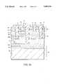
- FIGS. 1a, 1b and 1care sectional views, not to scale, showing three successive stages in the fabrication of a 3-D circuit assembly in accordance with the invention
- FIGS. 2a and 2bare sectional views, not to scale, illustrating successive steps in the fabrication of a circuit assembly with at least one additional circuit layer to those employed in FIGS. 1a-1b;
- FIG. 3is a sectional view, not to scale, of a focal plane array assembly that incorporates the invention.
- the present inventionmakes it possible to fabricate a 3-D circuit structure from two or more standard wafers, each of which has its own circuit layer.
- the first step in the preferred fabrication methodis illustrated in FIG. 1a.
- Two conventional bonded silicon wafers 2a and 2bare shown, with the upper wafer 2b inverted and secured to the lower wafer 2a by a thin layer of electrically insulating adhesive 4 that is cured after the wafers are positioned.
- Accurate wafer alignment techniquesare available that have been developed in connection with the known bump bonding technology mentioned above.
- Each waferincludes a relatively thick silicon substrate 6a, 6b, a thin electrically insulative silicon dioxide layer 8a, 8b on the silicon substrate, and a thin silicon-based IC layer 10a, 10b on the respective SiO 2 layer 8a and 8b.
- the insulator layer 8amay be omitted unless it is desired as an insulator for IC layer 10a. It is generally desirable to include insulator layer 8b, even if there is not a need for upper insulation of IC layer 10b, since layer 8b serves as an etch stop during the subsequent removal of the upper substrate 6b, as described below. Lower substrate 6a would not normally be removed, so insulator layer 8a serves only an insulating and not an etch stop function.
- Typical thicknesses for the elements of each bonded waferare 525 microns for the silicon substrates 6a, 6b, 0.2-2 microns for the SiO 2 layers 8a, 8b, and 0.2-2 microns for the IC layers 10a, 10b. Details of the actual circuitry fabricated in the IC layers are not shown, but generally the circuitry itself would extend about 0.3 microns deep into the IC layers and can include devices such as transistors, capacitors, etc.
- Aluminum contact pads 12a, 12bare provided on the circuit faces of the two wafers 2a, 2b for making electrical contacts to their respective ICs through openings in a thin insulating film (not shown).
- the circuitry on the two wafersmay be formed with different process techniques, such as bipolar vs. CMOS (complementary metal-oxide-semiconductor); since the wafers are provided as standard items before being bonded together, they can be fabricated totally independent of each other.
- CMOScomplementary metal-oxide-semiconductor
- silicon based circuitsare illustrated, other materials such as GaAs could also be used; one material could be used for one wafer and other material for the other wafer so long as they are compatible with the interconnections provided between the two.
- isolation layers 8a and 8baluminum nitride or silicon nitride might be substituted for silicon dioxide.
- the silicon substrates 6a, 6b and silicon-based IC layers 10a, 10bwill generally have similar coefficients of thermal expansion, but this coefficient will generally be different from the temperature coefficients for the isolation layers 8a, 8b and the adhesive 4. While this might ordinarily be expected to result in the possibility of cracking over the normal design temperature range of -55° C.-125° C., the adhesive layer 4 is kept to a few microns in thickness. The thin dimensions for both the adhesive and isolation layers cause them to effectively assume the thermal expansion coefficient of the much thicker silicon substrate 6a to which they are bonded, so that the thermal expansion and contraction of the adhesive and isolation layers is controlled by and generally matches the thermal expansion of the silicon substrate. This stretching of the thinner material layers inhibits either cracking or delamination when significant temperature differentials are encountered.
- a suitable material for the adhesive layer 4is produced by Ablestick, Inc. under the designation GA47-2LV.
- a fusible bonding materialsuch as high temperature glass could be used, with the wafers bonded together by heating the fusible material. In this event the thickness of the bonding layer would still preferably be restricted to a few microns.
- the upper substrate 6bhas been removed, preferably by etching it away while using the SiO 2 layer 8b as an etch stop.
- the substrate 6bcan be removed first and the remaining IC layer 10b and insulative layer 8b aligned to the underlying wafer 2a with the assistance of an intermediate carrier. Openings are then made through the assembly to access selected contact pads 12a, 12b, and thus expose a path to electrically contact the portions of the circuitry to which these pads are connected.
- the contact pad 12b for the IC layer 10bare accessed with via openings 14b through the upper SiO 2 layer 8b and IC layer 10b, while the contact pads 12a for the lower IC layer 10a are accessed with via openings via 14a through the upper SiO 2 layer 8b, upper IC layer 10b and the adhesive layer 4.
- Presently available trenching techniquessuch as disclosed in Copper, et al., "Physical and Electrical Characteristics of Submicron Trench Capacitors", Extended Abstracts, The Electrochemical Society, Vol. 90-2, Oct. 14-19, 1990, pages 410-411; and U.S. Pat. No. 4,702,795 to Douglas, permit these openings to be kept to a few microns in diameter or less. Since the relatively thick upper substrate 6b has been removed before the openings are made, the openings need extend only through the thin layers 8b, 10b and 4, and thus any spreading is minimized.
- the via openings 14a and 14bcan be formed by either chemical etching or reactive ion etching. Although trenching to the contact pads 12a and 12b is illustrated, the via openings 14a and 14b could also be established to desired metallization locations directly on the ICs themselves; the metallization of either the ICs or contact pads are preferably used as an etch stop.
- the via opening locationsare controlled by a conventional mask technique, in which the upper SiO 2 layer 8b can function as the etch mask.
- FIG. 1cshows a later stage in the device's fabrication.
- the sidewalls of the via openingshave been coated with respective sleeves 16 of an insulative material such as glass (SiO 2 ).
- the sleeves 16are applied by a process such as chemical vapor deposition, with the insulative coating removed from the bottoms of the via openings preferably by a photoetching process, either reactive ion etching or hydrofluoric acid.
- a metallization 18, preferably aluminum,is then deposited over the upper surface of the SiO 2 layer 8b and into the via openings, through which it forms electrically conductive members that establish electrical connections to their respective contact pads 12a and 12b.
- the sleeves 16insulate the electrical contacts from the surrounding IC layer 10b.
- the metallization layer on the upper surface of SiO 2 layer 8bis next photoetched to establish desired interconnections between the contact pads for the two IC layers 10a and 10b.
- the metallization layermay be left intact so as to extend over the surface of SiO 2 layer 8b and interconnect a contact to one IC layer with a contact to the other; such an interconnection is indicated by numeral 20.
- the devicemay be considered to be essentially complete, and the wafer can be tested and diced using conventional techniques.
- the resultis a set of high density 3-D circuit chips that have a sturdy construction, are useable over the full normal temperature range, and can have different circuit layers that employ different circuitry processes and even different materials.
- FIGS. 2a and 2bA variation of the 3-D circuit package and fabrication technique of FIGS. 1a-1c is illustrated in FIGS. 2a and 2b.
- a third conventional bonded wafer 2chas been inverted and adhered to the SiO 2 isolation layer 8b of the wafer 2b, after the removal of the upper substrate 6b (FIG. 1a) from wafer 2b.
- the new wafer 2cconsists of a silicon (or other desired semiconductor) substrate 6c, an insulation layer 8c and an integrated circuit layer 10c with associated contact pads 12c. It is adhered to the underlying insulation layer 8b by a thin layer of adhesive or fusion bonded material 22 similar to the adherent material 4.
- the uppermost wafer's insulating layer 8c, IC layer 10c and adherent layer 22are again thin enough so that they each expand and contract along with the much thicker bottom substrate 6a.
- the substrate 6cis etched away.
- the substrate 6ccan be removed first and the remainder of the wafer aligned and adhered to the lower assembly with the assistance of an intermediate carrier. Openings are then etched to selected contact pads for the three different IC layers, as illustrated in FIG. 2b, in a manner similar to the formation of the access openings shown in FIG. 1c, and the openings are lined with insulating sleeves 16'.
- a metallization 18'is then applied to the upper surface of the top SiO 2 layer 8c and into the access openings, where it is insulated from the surrounding IC layers by the insulating sleeves.
- the metallization 18'is etched to leave desired metal interconnects 20' extending across the surface of upper SiO 2 layer 8c and thereby interconnect selected contact pads at different levels in the device, while removing the metallization from the areas where it is not needed.
- Additional IC layerscan be added in a similar fashion. However, the circuit density achievable with each additional layer will be progressively reduced somewhat, since the upper IC layers are traversed by both their own leads (if their contact pads are on their underside) and by the leads for all of the lower IC layers. Furthermore, since the provision of additional layers increases the total thickness of the material that must be etched to access the lower IC layers, the access openings for those layers will tend to spread somewhat as they approach the upper surface of the package, thus further reducing the area available for circuitry in the upper layers.
- FIG. 3Another application of the invention is for the detection of electromagnetic radiation, such as with an infrared focal plane array.
- a lower substrate 24 formed from a suitable photodetector materialsuch as HgCdTe/CdTe is used to sense IR radiation that strikes the underside of the package.
- the photodetectioncan be accomplished either with a photoconductive material whose resistance is sensitive to radiation, or with a photovoltaic material whose voltage is sensitive to radiation.
- the radiationfirst passes through an anti-reflection coating sheet 26 on substrate 24, which is organized into a matrix of pixels, each pixel being provided with a respective pixel contact pad 12a on the upper surface of the substrate.
- a photoconductive substrateWith a photoconductive substrate, a voltage is supplied to electrode 26 and the voltage drop across the substrate 24 is determined for each pixel by the amount that pixel is illuminated by the radiation of interest.
- a contactWith a photovoltaic substrate, a contact (not shown) is made to the same surface of substrate 24 as the contacts 12a, and a voltage is dropped across photodiode depletion region of substrate 24.
- the IC layer 10b and insulative layer 8b of the upper wafer 2bare adhered to the photodetector substrate 24 in a manner similar to the previously described embodiments.
- the readout circuitry for the focal plane arrayis provided in the IC layer 10b, and is interconnected with the various pixel contact pads 12a by metallized interconnections as in the previous embodiments.
- the resultis a unitary focal plane array package that has a capacity for a high density readout circuitry layer integrated with the photodetector. If desired, additional layers of readout circuitry can be provided as illustrated in FIGS. 2a and 2b.
Landscapes
- Engineering & Computer Science (AREA)
- Microelectronics & Electronic Packaging (AREA)
- Power Engineering (AREA)
- Physics & Mathematics (AREA)
- Condensed Matter Physics & Semiconductors (AREA)
- General Physics & Mathematics (AREA)
- Computer Hardware Design (AREA)
- Manufacturing & Machinery (AREA)
- Internal Circuitry In Semiconductor Integrated Circuit Devices (AREA)
Abstract
Description
Claims (11)
Priority Applications (1)
| Application Number | Priority Date | Filing Date | Title |
|---|---|---|---|
| US08/192,207US5489554A (en) | 1992-07-21 | 1994-02-04 | Method of making a 3-dimensional circuit assembly having electrical contacts that extend through the IC layer |
Applications Claiming Priority (2)
| Application Number | Priority Date | Filing Date | Title |
|---|---|---|---|
| US91834392A | 1992-07-21 | 1992-07-21 | |
| US08/192,207US5489554A (en) | 1992-07-21 | 1994-02-04 | Method of making a 3-dimensional circuit assembly having electrical contacts that extend through the IC layer |
Related Parent Applications (1)
| Application Number | Title | Priority Date | Filing Date |
|---|---|---|---|
| US91834392ADivision | 1992-07-21 | 1992-07-21 |
Publications (1)
| Publication Number | Publication Date |
|---|---|
| US5489554Atrue US5489554A (en) | 1996-02-06 |
Family
ID=25440219
Family Applications (1)
| Application Number | Title | Priority Date | Filing Date |
|---|---|---|---|
| US08/192,207Expired - LifetimeUS5489554A (en) | 1992-07-21 | 1994-02-04 | Method of making a 3-dimensional circuit assembly having electrical contacts that extend through the IC layer |
Country Status (1)
| Country | Link |
|---|---|
| US (1) | US5489554A (en) |
Cited By (60)
| Publication number | Priority date | Publication date | Assignee | Title |
|---|---|---|---|---|
| US5563084A (en)* | 1994-09-22 | 1996-10-08 | Fraunhofer-Gesellschaft zur F orderung der angewandten Forschung e.V. | Method of making a three-dimensional integrated circuit |
| US5766984A (en)* | 1994-09-22 | 1998-06-16 | Fraunhofer-Gesellschaft Zur Foerderung Der Angewandten Forschung | Method of making a vertical integrated circuit |
| DE19702121C1 (en)* | 1997-01-22 | 1998-06-18 | Siemens Ag | Vertical chip interconnection production |
| US5882986A (en)* | 1998-03-30 | 1999-03-16 | General Semiconductor, Inc. | Semiconductor chips having a mesa structure provided by sawing |
| US5904495A (en)* | 1997-06-11 | 1999-05-18 | Massachusetts Institute Of Technology | Interconnection technique for hybrid integrated devices |
| EP0948808A4 (en)* | 1996-10-29 | 2000-05-10 | Trusi Technologies Llc | INTEGRATED CIRCUITS AND MANUFACTURING METHODS THEREOF |
| US6090636A (en)* | 1998-02-26 | 2000-07-18 | Micron Technology, Inc. | Integrated circuits using optical waveguide interconnects formed through a semiconductor wafer and methods for forming same |
| US6150188A (en)* | 1998-02-26 | 2000-11-21 | Micron Technology Inc. | Integrated circuits using optical fiber interconnects formed through a semiconductor wafer and methods for forming same |
| US20010006257A1 (en)* | 1999-09-24 | 2001-07-05 | Chian-Gauh Shih | Method of fabricating a three-dimensional system-on-chip and its structure |
| US6284627B1 (en)* | 1997-09-19 | 2001-09-04 | Fraunhofer-Gesellschaft zur Förderung der angewandten Forschung e.V. | Method for wiring semi-conductor components in order to prevent product piracy and manipulation, semi-conductors component made according to this method and use of said semi-conductor component in a chip card |
| US6287940B1 (en)* | 1999-08-02 | 2001-09-11 | Honeywell International Inc. | Dual wafer attachment process |
| WO2001071797A1 (en)* | 2000-03-22 | 2001-09-27 | Ziptronix, Inc. | Three dimensional device integration method and integrated device |
| US6322903B1 (en) | 1999-12-06 | 2001-11-27 | Tru-Si Technologies, Inc. | Package of integrated circuits and vertical integration |
| US20020084513A1 (en)* | 1996-10-29 | 2002-07-04 | Oleg Siniaguine | Integrated circuits and methods for their fabrication |
| US20020094661A1 (en)* | 1999-10-01 | 2002-07-18 | Ziptronix | Three dimensional device intergration method and intergrated device |
| US6503778B1 (en)* | 1999-09-28 | 2003-01-07 | Sony Corporation | Thin film device and method of manufacturing the same |
| US20030057564A1 (en)* | 1997-04-04 | 2003-03-27 | Elm Technology Corporation | Three dimensional structure memory |
| US20030062123A1 (en)* | 2001-09-28 | 2003-04-03 | Hrl Laboratories, Llc | Method of self-latching for adhesion during self-assembly of electronic or optical components |
| US20030112576A1 (en)* | 2001-09-28 | 2003-06-19 | Brewer Peter D. | Process for producing high performance interconnects |
| US6600173B2 (en) | 2000-08-30 | 2003-07-29 | Cornell Research Foundation, Inc. | Low temperature semiconductor layering and three-dimensional electronic circuits using the layering |
| US20030141502A1 (en)* | 2000-08-09 | 2003-07-31 | Ziptronix | Method of epitaxial-like wafer bonding at low temperature and bonded structure |
| US20030186486A1 (en)* | 2002-03-28 | 2003-10-02 | Swan Johanna M. | Integrated circuit die and an electronic assembly having a three-dimensional interconnection scheme |
| US20030183943A1 (en)* | 2002-03-28 | 2003-10-02 | Swan Johanna M. | Integrated circuit die and an electronic assembly having a three-dimensional interconnection scheme |
| US6632706B1 (en) | 1997-04-04 | 2003-10-14 | Elm Technology Corporation | Three dimensional structure integrated circuit fabrication process |
| US20030205407A1 (en)* | 2002-02-04 | 2003-11-06 | Brist Gary A. | Power-ground plane partitioning and via connection to utilize channel/trenches for power delivery |
| US20030211705A1 (en)* | 2000-02-16 | 2003-11-13 | Ziptronix, Inc. | Method for low temperature bonding and bonded structure |
| US20030218182A1 (en)* | 1992-04-08 | 2003-11-27 | Leedy Glenn J. | Strees-controlled dielectric integrated circuit |
| US20030223535A1 (en)* | 1992-04-08 | 2003-12-04 | Leedy Glenn Joseph | Lithography device for semiconductor circuit pattern generator |
| EP1387401A2 (en)* | 1996-10-29 | 2004-02-04 | Trusi Technologies, Llc | Integrated circuits and methods for their fabrication |
| US6709978B2 (en) | 1998-01-20 | 2004-03-23 | Micron Technology, Inc. | Method for forming integrated circuits using high aspect ratio vias through a semiconductor wafer |
| US6717254B2 (en) | 2001-02-22 | 2004-04-06 | Tru-Si Technologies, Inc. | Devices having substrates with opening passing through the substrates and conductors in the openings, and methods of manufacture |
| US20040108071A1 (en)* | 2001-04-11 | 2004-06-10 | Thomas Wien | Label applicator and system |
| US20040113245A1 (en)* | 2000-03-24 | 2004-06-17 | Yuji Takaoka | Semiconductor device and process for fabricating the same |
| US6753205B2 (en) | 2001-09-13 | 2004-06-22 | Tru-Si Technologies, Inc. | Method for manufacturing a structure comprising a substrate with a cavity and a semiconductor integrated circuit bonded to a contact pad located in the cavity |
| US6790704B2 (en)* | 1997-12-29 | 2004-09-14 | Intel Corporation | Method for capacitively coupling electronic devices |
| US6848177B2 (en) | 2002-03-28 | 2005-02-01 | Intel Corporation | Integrated circuit die and an electronic assembly having a three-dimensional interconnection scheme |
| US20050023656A1 (en)* | 2002-08-08 | 2005-02-03 | Leedy Glenn J. | Vertical system integration |
| US20050121765A1 (en)* | 2003-12-09 | 2005-06-09 | Advanced Semiconductor Engineering, Inc. | Multi-chips bumpless assembly package and manufacturing method thereof |
| DE19746641B4 (en)* | 1997-09-19 | 2006-02-23 | Fraunhofer-Gesellschaft zur Förderung der angewandten Forschung e.V. | Wiring method for semiconductor devices for preventing product piracy and product manipulation and use of the semiconductor device in a smart card |
| US7223635B1 (en) | 2003-07-25 | 2007-05-29 | Hrl Laboratories, Llc | Oriented self-location of microstructures with alignment structures |
| US7253091B2 (en)* | 2001-09-28 | 2007-08-07 | Hrl Laboratories, Llc | Process for assembling three-dimensional systems on a chip and structure thus obtained |
| US20070218678A1 (en)* | 2006-03-17 | 2007-09-20 | Min Suk Suh | Method of manufacturing wafer level stack package |
| US20080150153A1 (en)* | 2003-10-21 | 2008-06-26 | Ziptronix, Inc. | Single mask via method and device |
| US20100264551A1 (en)* | 2009-04-20 | 2010-10-21 | International Business Machines Corporation | Three dimensional integrated circuit integration using dielectric bonding first and through via formation last |
| US20110057321A1 (en)* | 2009-09-08 | 2011-03-10 | Industrial Technology Research Institute | 3-d multi-wafer stacked semiconductor structure and method for manufacturing the same |
| DE102012108522A1 (en)* | 2012-09-12 | 2014-03-13 | Ams Ag | Method for manufacturing semiconductor stack for stacking semiconductor chips with components for three-dimensional integration of electronic circuit, involves arranging through-contacts in aperture after connecting stack components |
| US20160181155A1 (en)* | 2014-12-22 | 2016-06-23 | Commissariat A L'energie Atomique Et Aux Energies Alternatives | Method for making an integrated circuit in three dimensions |
| KR20160099457A (en)* | 2015-02-12 | 2016-08-22 | 타이완 세미콘덕터 매뉴팩쳐링 컴퍼니 리미티드 | Integrated circuit stack verification method and system for performing the same |
| US20160314998A1 (en)* | 2015-04-20 | 2016-10-27 | Kabushiki Kaisha Toshiba | Manufacturing apparatus and manufacturing method of semiconductor device |
| US20170317011A1 (en)* | 2010-04-28 | 2017-11-02 | Taiwan Semiconductor Manufacturing Company, Ltd. | Through-Substrate Vias with Improved Connections |
| US10418311B2 (en)* | 2017-03-28 | 2019-09-17 | Micron Technology, Inc. | Method of forming vias using silicon on insulator substrate |
| CN111834312A (en)* | 2020-07-29 | 2020-10-27 | 华进半导体封装先导技术研发中心有限公司 | Three-dimensional stacking structure based on TSV (through silicon via) process and manufacturing method |
| US20220037235A1 (en)* | 2020-07-31 | 2022-02-03 | Samsung Electronics Co., Ltd. | Semiconductor device |
| US20220044962A1 (en)* | 2011-04-19 | 2022-02-10 | Sony Group Corporation | Semiconductor device, manufacturing method thereof, solid-state imaging device, and electronic apparatus |
| US11562984B1 (en) | 2020-10-14 | 2023-01-24 | Hrl Laboratories, Llc | Integrated mechanical aids for high accuracy alignable-electrical contacts |
| US11600519B2 (en)* | 2019-09-16 | 2023-03-07 | International Business Machines Corporation | Skip-via proximity interconnect |
| US11760059B2 (en) | 2003-05-19 | 2023-09-19 | Adeia Semiconductor Bonding Technologies Inc. | Method of room temperature covalent bonding |
| US12057429B1 (en) | 2021-06-23 | 2024-08-06 | Hrl Laboratories, Llc | Temporary bonding structures for die-to-die and wafer-to-wafer bonding |
| US12424584B2 (en) | 2020-10-29 | 2025-09-23 | Adeia Semiconductor Bonding Technologies Inc. | Direct bonding methods and structures |
| US12444712B1 (en) | 2022-12-06 | 2025-10-14 | Hrl Laboratories, Llc | Integrated mechanical aids for high accuracy alignable-electrical contacts |
Citations (15)
| Publication number | Priority date | Publication date | Assignee | Title |
|---|---|---|---|---|
| US3648131A (en)* | 1969-11-07 | 1972-03-07 | Ibm | Hourglass-shaped conductive connection through semiconductor structures |
| US4122479A (en)* | 1975-01-31 | 1978-10-24 | Hitachi, Ltd. | Optoelectronic device having control circuit for light emitting element and circuit for light receiving element integrated in a semiconductor body |
| US4467340A (en)* | 1981-11-16 | 1984-08-21 | Rockwell International Corporation | Pre-multiplexed Schottky barrier focal plane |
| JPS61125150A (en)* | 1984-11-22 | 1986-06-12 | Agency Of Ind Science & Technol | Manufacture of three dimensional semiconductor device |
| US4612083A (en)* | 1984-07-20 | 1986-09-16 | Nec Corporation | Process of fabricating three-dimensional semiconductor device |
| JPS63213943A (en)* | 1987-03-03 | 1988-09-06 | Sharp Corp | Method for manufacturing three-dimensional semiconductor integrated circuit |
| JPS63300510A (en)* | 1987-05-30 | 1988-12-07 | Agency Of Ind Science & Technol | Laminated semiconductor device |
| US4829018A (en)* | 1986-06-27 | 1989-05-09 | Wahlstrom Sven E | Multilevel integrated circuits employing fused oxide layers |
| US5122856A (en)* | 1987-11-13 | 1992-06-16 | Nissan Motor Co., Ltd. | Semiconductor device |
| US5191405A (en)* | 1988-12-23 | 1993-03-02 | Matsushita Electric Industrial Co., Ltd. | Three-dimensional stacked lsi |
| JPH0555455A (en)* | 1991-08-27 | 1993-03-05 | Seiko Instr Inc | Manufacture of semiconductor device |
| US5227013A (en)* | 1991-07-25 | 1993-07-13 | Microelectronics And Computer Technology Corporation | Forming via holes in a multilevel substrate in a single step |
| US5229647A (en)* | 1991-03-27 | 1993-07-20 | Micron Technology, Inc. | High density data storage using stacked wafers |
| US5236871A (en)* | 1992-04-29 | 1993-08-17 | The United States Of America As Represented By The Administrator Of The National Aeronautics And Space Administration | Method for producing a hybridization of detector array and integrated circuit for readout |
| US5270261A (en)* | 1991-09-13 | 1993-12-14 | International Business Machines Corporation | Three dimensional multichip package methods of fabrication |
- 1994
- 1994-02-04USUS08/192,207patent/US5489554A/ennot_activeExpired - Lifetime
Patent Citations (15)
| Publication number | Priority date | Publication date | Assignee | Title |
|---|---|---|---|---|
| US3648131A (en)* | 1969-11-07 | 1972-03-07 | Ibm | Hourglass-shaped conductive connection through semiconductor structures |
| US4122479A (en)* | 1975-01-31 | 1978-10-24 | Hitachi, Ltd. | Optoelectronic device having control circuit for light emitting element and circuit for light receiving element integrated in a semiconductor body |
| US4467340A (en)* | 1981-11-16 | 1984-08-21 | Rockwell International Corporation | Pre-multiplexed Schottky barrier focal plane |
| US4612083A (en)* | 1984-07-20 | 1986-09-16 | Nec Corporation | Process of fabricating three-dimensional semiconductor device |
| JPS61125150A (en)* | 1984-11-22 | 1986-06-12 | Agency Of Ind Science & Technol | Manufacture of three dimensional semiconductor device |
| US4829018A (en)* | 1986-06-27 | 1989-05-09 | Wahlstrom Sven E | Multilevel integrated circuits employing fused oxide layers |
| JPS63213943A (en)* | 1987-03-03 | 1988-09-06 | Sharp Corp | Method for manufacturing three-dimensional semiconductor integrated circuit |
| JPS63300510A (en)* | 1987-05-30 | 1988-12-07 | Agency Of Ind Science & Technol | Laminated semiconductor device |
| US5122856A (en)* | 1987-11-13 | 1992-06-16 | Nissan Motor Co., Ltd. | Semiconductor device |
| US5191405A (en)* | 1988-12-23 | 1993-03-02 | Matsushita Electric Industrial Co., Ltd. | Three-dimensional stacked lsi |
| US5229647A (en)* | 1991-03-27 | 1993-07-20 | Micron Technology, Inc. | High density data storage using stacked wafers |
| US5227013A (en)* | 1991-07-25 | 1993-07-13 | Microelectronics And Computer Technology Corporation | Forming via holes in a multilevel substrate in a single step |
| JPH0555455A (en)* | 1991-08-27 | 1993-03-05 | Seiko Instr Inc | Manufacture of semiconductor device |
| US5270261A (en)* | 1991-09-13 | 1993-12-14 | International Business Machines Corporation | Three dimensional multichip package methods of fabrication |
| US5236871A (en)* | 1992-04-29 | 1993-08-17 | The United States Of America As Represented By The Administrator Of The National Aeronautics And Space Administration | Method for producing a hybridization of detector array and integrated circuit for readout |
Cited By (210)
| Publication number | Priority date | Publication date | Assignee | Title |
|---|---|---|---|---|
| US7307020B2 (en) | 1992-04-08 | 2007-12-11 | Elm Technology Corporation | Membrane 3D IC fabrication |
| US7385835B2 (en) | 1992-04-08 | 2008-06-10 | Elm Technology Corporation | Membrane 3D IC fabrication |
| US20030223535A1 (en)* | 1992-04-08 | 2003-12-04 | Leedy Glenn Joseph | Lithography device for semiconductor circuit pattern generator |
| US20040132303A1 (en)* | 1992-04-08 | 2004-07-08 | Elm Technology Corporation | Membrane 3D IC fabrication |
| US7550805B2 (en) | 1992-04-08 | 2009-06-23 | Elm Technology Corporation | Stress-controlled dielectric integrated circuit |
| US7615837B2 (en) | 1992-04-08 | 2009-11-10 | Taiwan Semiconductor Manufacturing Company | Lithography device for semiconductor circuit pattern generation |
| US20040192045A1 (en)* | 1992-04-08 | 2004-09-30 | Elm Technology Corporation. | Apparatus and methods for maskless pattern generation |
| US7485571B2 (en) | 1992-04-08 | 2009-02-03 | Elm Technology Corporation | Method of making an integrated circuit |
| US7479694B2 (en) | 1992-04-08 | 2009-01-20 | Elm Technology Corporation | Membrane 3D IC fabrication |
| US20040197951A1 (en)* | 1992-04-08 | 2004-10-07 | Leedy Glenn Joseph | Membrane IC fabrication |
| US20080302559A1 (en)* | 1992-04-08 | 2008-12-11 | Elm Technology Corporation | Flexible and elastic dielectric integrated circuit |
| US7670893B2 (en) | 1992-04-08 | 2010-03-02 | Taiwan Semiconductor Manufacturing Co., Ltd. | Membrane IC fabrication |
| US7763948B2 (en) | 1992-04-08 | 2010-07-27 | Taiwan Semiconductor Manufacturing Co., Ltd. | Flexible and elastic dielectric integrated circuit |
| US7820469B2 (en) | 1992-04-08 | 2010-10-26 | Taiwan Semiconductor Manufacturing Co., Ltd. | Stress-controlled dielectric integrated circuit |
| US20050082626A1 (en)* | 1992-04-08 | 2005-04-21 | Elm Technology Corporation | Membrane 3D IC fabrication |
| US20050082641A1 (en)* | 1992-04-08 | 2005-04-21 | Elm Technology Corporation | Flexible and elastic dielectric integrated circuit |
| US20050130351A1 (en)* | 1992-04-08 | 2005-06-16 | Elm Technology Corporation | Methods for maskless lithography |
| US7911012B2 (en) | 1992-04-08 | 2011-03-22 | Taiwan Semiconductor Manufacturing Co., Ltd. | Flexible and elastic dielectric integrated circuit |
| US20050176174A1 (en)* | 1992-04-08 | 2005-08-11 | Elm Technology Corporation | Methodof making an integrated circuit |
| US20030218182A1 (en)* | 1992-04-08 | 2003-11-27 | Leedy Glenn J. | Strees-controlled dielectric integrated circuit |
| US7176545B2 (en) | 1992-04-08 | 2007-02-13 | Elm Technology Corporation | Apparatus and methods for maskless pattern generation |
| US7223696B2 (en) | 1992-04-08 | 2007-05-29 | Elm Technology Corporation | Methods for maskless lithography |
| US7242012B2 (en) | 1992-04-08 | 2007-07-10 | Elm Technology Corporation | Lithography device for semiconductor circuit pattern generator |
| US5766984A (en)* | 1994-09-22 | 1998-06-16 | Fraunhofer-Gesellschaft Zur Foerderung Der Angewandten Forschung | Method of making a vertical integrated circuit |
| US5563084A (en)* | 1994-09-22 | 1996-10-08 | Fraunhofer-Gesellschaft zur F orderung der angewandten Forschung e.V. | Method of making a three-dimensional integrated circuit |
| US6184060B1 (en) | 1996-10-29 | 2001-02-06 | Trusi Technologies Llc | Integrated circuits and methods for their fabrication |
| EP1503406A2 (en) | 1996-10-29 | 2005-02-02 | Tru-Si Technologies, Inc. | Back-side contact pads of a semiconductor chip |
| US6420209B1 (en) | 1996-10-29 | 2002-07-16 | Tru-Si Technologies, Inc. | Integrated circuits and methods for their fabrication |
| US20020084513A1 (en)* | 1996-10-29 | 2002-07-04 | Oleg Siniaguine | Integrated circuits and methods for their fabrication |
| EP2270845A3 (en)* | 1996-10-29 | 2013-04-03 | Invensas Corporation | Integrated circuits and methods for their fabrication |
| EP2270846A3 (en)* | 1996-10-29 | 2011-12-21 | ALLVIA, Inc. | Integrated circuits and methods for their fabrication |
| US6882030B2 (en) | 1996-10-29 | 2005-04-19 | Tru-Si Technologies, Inc. | Integrated circuit structures with a conductor formed in a through hole in a semiconductor substrate and protruding from a surface of the substrate |
| US20020127868A1 (en)* | 1996-10-29 | 2002-09-12 | Oleg Siniaguine | Integrated circuits and methods for their fabrication |
| EP0948808A4 (en)* | 1996-10-29 | 2000-05-10 | Trusi Technologies Llc | INTEGRATED CIRCUITS AND MANUFACTURING METHODS THEREOF |
| US6639303B2 (en) | 1996-10-29 | 2003-10-28 | Tru-Si Technolgies, Inc. | Integrated circuits and methods for their fabrication |
| US6740582B2 (en) | 1996-10-29 | 2004-05-25 | Tru-Si Technologies, Inc. | Integrated circuits and methods for their fabrication |
| EP1387401A2 (en)* | 1996-10-29 | 2004-02-04 | Trusi Technologies, Llc | Integrated circuits and methods for their fabrication |
| US6664129B2 (en) | 1996-10-29 | 2003-12-16 | Tri-Si Technologies, Inc. | Integrated circuits and methods for their fabrication |
| WO1998033216A1 (en)* | 1997-01-22 | 1998-07-30 | Siemens Aktiengesellschaft | Method for producing vertical chip connections |
| DE19702121C1 (en)* | 1997-01-22 | 1998-06-18 | Siemens Ag | Vertical chip interconnection production |
| US8410617B2 (en) | 1997-04-04 | 2013-04-02 | Elm Technology | Three dimensional structure memory |
| US8841778B2 (en) | 1997-04-04 | 2014-09-23 | Glenn J Leedy | Three dimensional memory structure |
| US20090219744A1 (en)* | 1997-04-04 | 2009-09-03 | Leedy Glenn J | Three dimensional structure memory |
| US20090218700A1 (en)* | 1997-04-04 | 2009-09-03 | Leedy Glenn J | Three dimensional structure memory |
| US6632706B1 (en) | 1997-04-04 | 2003-10-14 | Elm Technology Corporation | Three dimensional structure integrated circuit fabrication process |
| US20030057564A1 (en)* | 1997-04-04 | 2003-03-27 | Elm Technology Corporation | Three dimensional structure memory |
| US8288206B2 (en) | 1997-04-04 | 2012-10-16 | Elm Technology Corp | Three dimensional structure memory |
| US20040070063A1 (en)* | 1997-04-04 | 2004-04-15 | Elm Technology Corporation | Three dimensional structure integrated circuit |
| US7193239B2 (en) | 1997-04-04 | 2007-03-20 | Elm Technology Corporation | Three dimensional structure integrated circuit |
| US20040097008A1 (en)* | 1997-04-04 | 2004-05-20 | Elm Technology Corporation | Three dimensional structure integrated circuit |
| US20090219743A1 (en)* | 1997-04-04 | 2009-09-03 | Leedy Glenn J | Three dimensional structure memory |
| US9087556B2 (en) | 1997-04-04 | 2015-07-21 | Glenn J Leedy | Three dimension structure memory |
| US20090175104A1 (en)* | 1997-04-04 | 2009-07-09 | Leedy Glenn J | Three dimensional structure memory |
| US6551857B2 (en) | 1997-04-04 | 2003-04-22 | Elm Technology Corporation | Three dimensional structure integrated circuits |
| US9401183B2 (en) | 1997-04-04 | 2016-07-26 | Glenn J. Leedy | Stacked integrated memory device |
| US20040151043A1 (en)* | 1997-04-04 | 2004-08-05 | Elm Technology Corporation | Three dimensional structure memory |
| US7138295B2 (en) | 1997-04-04 | 2006-11-21 | Elm Technology Corporation | Method of information processing using three dimensional integrated circuits |
| US8035233B2 (en) | 1997-04-04 | 2011-10-11 | Elm Technology Corporation | Adjacent substantially flexible substrates having integrated circuits that are bonded together by non-polymeric layer |
| US8933570B2 (en) | 1997-04-04 | 2015-01-13 | Elm Technology Corp. | Three dimensional structure memory |
| US8629542B2 (en) | 1997-04-04 | 2014-01-14 | Glenn J. Leedy | Three dimensional structure memory |
| US8791581B2 (en) | 1997-04-04 | 2014-07-29 | Glenn J Leedy | Three dimensional structure memory |
| US20030173608A1 (en)* | 1997-04-04 | 2003-09-18 | Elm Technology Corporation | Three dimensional structure integrated circuit |
| US8928119B2 (en) | 1997-04-04 | 2015-01-06 | Glenn J. Leedy | Three dimensional structure memory |
| US7504732B2 (en) | 1997-04-04 | 2009-03-17 | Elm Technology Corporation | Three dimensional structure memory |
| US8907499B2 (en) | 1997-04-04 | 2014-12-09 | Glenn J Leedy | Three dimensional structure memory |
| US20090067210A1 (en)* | 1997-04-04 | 2009-03-12 | Leedy Glenn J | Three dimensional structure memory |
| US20100171224A1 (en)* | 1997-04-04 | 2010-07-08 | Leedy Glenn J | Three dimensional structure memory |
| US20100173453A1 (en)* | 1997-04-04 | 2010-07-08 | Leedy Glenn J | Three dimensional structure memory |
| US7705466B2 (en) | 1997-04-04 | 2010-04-27 | Elm Technology Corporation | Three dimensional multi layer memory and control logic integrated circuit structure |
| US7474004B2 (en) | 1997-04-04 | 2009-01-06 | Elm Technology Corporation | Three dimensional structure memory |
| US8318538B2 (en) | 1997-04-04 | 2012-11-27 | Elm Technology Corp. | Three dimensional structure memory |
| US6563224B2 (en) | 1997-04-04 | 2003-05-13 | Elm Technology Corporation | Three dimensional structure integrated circuit |
| US8824159B2 (en) | 1997-04-04 | 2014-09-02 | Glenn J. Leedy | Three dimensional structure memory |
| US8796862B2 (en) | 1997-04-04 | 2014-08-05 | Glenn J Leedy | Three dimensional memory structure |
| US5904495A (en)* | 1997-06-11 | 1999-05-18 | Massachusetts Institute Of Technology | Interconnection technique for hybrid integrated devices |
| DE19746641B4 (en)* | 1997-09-19 | 2006-02-23 | Fraunhofer-Gesellschaft zur Förderung der angewandten Forschung e.V. | Wiring method for semiconductor devices for preventing product piracy and product manipulation and use of the semiconductor device in a smart card |
| US6284627B1 (en)* | 1997-09-19 | 2001-09-04 | Fraunhofer-Gesellschaft zur Förderung der angewandten Forschung e.V. | Method for wiring semi-conductor components in order to prevent product piracy and manipulation, semi-conductors component made according to this method and use of said semi-conductor component in a chip card |
| US6790704B2 (en)* | 1997-12-29 | 2004-09-14 | Intel Corporation | Method for capacitively coupling electronic devices |
| US6709978B2 (en) | 1998-01-20 | 2004-03-23 | Micron Technology, Inc. | Method for forming integrated circuits using high aspect ratio vias through a semiconductor wafer |
| US6526191B1 (en) | 1998-02-26 | 2003-02-25 | Micron Technology, Inc. | Integrated circuits using optical fiber interconnects formed through a semiconductor wafer and methods for forming same |
| US6150188A (en)* | 1998-02-26 | 2000-11-21 | Micron Technology Inc. | Integrated circuits using optical fiber interconnects formed through a semiconductor wafer and methods for forming same |
| US6090636A (en)* | 1998-02-26 | 2000-07-18 | Micron Technology, Inc. | Integrated circuits using optical waveguide interconnects formed through a semiconductor wafer and methods for forming same |
| US20030197186A1 (en)* | 1998-02-26 | 2003-10-23 | Micron Technology, Inc. | Integrated circuits using optical waveguide interconnects formed through a semiconductor wafer and methods for forming same |
| US20060131684A1 (en)* | 1998-02-26 | 2006-06-22 | Micron Technology, Inc. | Integrated circuits using optical waveguide interconnects formed through a semiconductor wafer and methods for forming same |
| US6723577B1 (en) | 1998-02-26 | 2004-04-20 | Micron Technology, Inc. | Method of forming an optical fiber interconnect through a semiconductor wafer |
| US6995443B2 (en) | 1998-02-26 | 2006-02-07 | Micron Technology, Inc. | Integrated circuits using optical fiber interconnects formed through a semiconductor wafer |
| US6777715B1 (en) | 1998-02-26 | 2004-08-17 | Micron Technology, Inc. | Integrated circuits using optical waveguide interconnects formed through a semiconductor wafer and methods for forming same |
| US7547954B2 (en) | 1998-02-26 | 2009-06-16 | Micron Technology, Inc. | Electronic systems using optical waveguide interconnects formed through a semiconductor wafer |
| US20070114543A1 (en)* | 1998-02-26 | 2007-05-24 | Micron Technology, Inc. | Electronic systems using optical waveguide interconnects formed through a semiconductor wafer |
| US7164156B2 (en) | 1998-02-26 | 2007-01-16 | Micron Technology, Inc. | Electronic systems using optical waveguide interconnects formed throught a semiconductor wafer |
| US6995441B2 (en) | 1998-02-26 | 2006-02-07 | Micron Technology, Inc. | Integrated circuits using optical waveguide interconnects formed through a semiconductor wafer and methods for forming same |
| US5882986A (en)* | 1998-03-30 | 1999-03-16 | General Semiconductor, Inc. | Semiconductor chips having a mesa structure provided by sawing |
| EP1198835B1 (en)* | 1999-08-02 | 2015-11-11 | Honeywell Inc. | Dual wafer attachment process |
| US6287940B1 (en)* | 1999-08-02 | 2001-09-11 | Honeywell International Inc. | Dual wafer attachment process |
| US20010006257A1 (en)* | 1999-09-24 | 2001-07-05 | Chian-Gauh Shih | Method of fabricating a three-dimensional system-on-chip and its structure |
| US6593645B2 (en)* | 1999-09-24 | 2003-07-15 | United Microelectronics Corp. | Three-dimensional system-on-chip structure |
| US6503778B1 (en)* | 1999-09-28 | 2003-01-07 | Sony Corporation | Thin film device and method of manufacturing the same |
| US7126212B2 (en) | 1999-10-01 | 2006-10-24 | Ziptronix, Inc. | Three dimensional device integration method and integrated device |
| US20080061419A1 (en)* | 1999-10-01 | 2008-03-13 | Ziptronix | Three dimensional device integration method and integrated device |
| US6984571B1 (en) | 1999-10-01 | 2006-01-10 | Ziptronix, Inc. | Three dimensional device integration method and integrated device |
| US20060292744A1 (en)* | 1999-10-01 | 2006-12-28 | Ziptronix | Three dimensional device integration method and integrated device |
| US10366962B2 (en) | 1999-10-01 | 2019-07-30 | Invensas Bonding Technologies, Inc. | Three dimensional device integration method and integrated device |
| US9431368B2 (en) | 1999-10-01 | 2016-08-30 | Ziptronix, Inc. | Three dimensional device integration method and integrated device |
| US9564414B2 (en) | 1999-10-01 | 2017-02-07 | Ziptronix, Inc. | Three dimensional device integration method and integrated device |
| US20020094661A1 (en)* | 1999-10-01 | 2002-07-18 | Ziptronix | Three dimensional device intergration method and intergrated device |
| US6322903B1 (en) | 1999-12-06 | 2001-11-27 | Tru-Si Technologies, Inc. | Package of integrated circuits and vertical integration |
| US9391143B2 (en) | 2000-02-16 | 2016-07-12 | Ziptronix, Inc. | Method for low temperature bonding and bonded structure |
| US20040152282A1 (en)* | 2000-02-16 | 2004-08-05 | Ziptronix, Inc. | Method for low temperature bonding and bonded structure |
| US7335572B2 (en) | 2000-02-16 | 2008-02-26 | Ziptronix, Inc. | Method for low temperature bonding and bonded structure |
| US9082627B2 (en) | 2000-02-16 | 2015-07-14 | Ziptronix, Inc. | Method for low temperature bonding and bonded structure |
| US7387944B2 (en) | 2000-02-16 | 2008-06-17 | Ziptronix, Inc. | Method for low temperature bonding and bonded structure |
| US8053329B2 (en) | 2000-02-16 | 2011-11-08 | Ziptronix, Inc. | Method for low temperature bonding and bonded structure |
| US20030211705A1 (en)* | 2000-02-16 | 2003-11-13 | Ziptronix, Inc. | Method for low temperature bonding and bonded structure |
| US7041178B2 (en) | 2000-02-16 | 2006-05-09 | Ziptronix, Inc. | Method for low temperature bonding and bonded structure |
| US9331149B2 (en) | 2000-02-16 | 2016-05-03 | Ziptronix, Inc. | Method for low temperature bonding and bonded structure |
| US8153505B2 (en) | 2000-02-16 | 2012-04-10 | Ziptronix, Inc. | Method for low temperature bonding and bonded structure |
| US10312217B2 (en) | 2000-02-16 | 2019-06-04 | Invensas Bonding Technologies, Inc. | Method for low temperature bonding and bonded structure |
| US6902987B1 (en) | 2000-02-16 | 2005-06-07 | Ziptronix, Inc. | Method for low temperature bonding and bonded structure |
| US20050079712A1 (en)* | 2000-02-16 | 2005-04-14 | Ziptronix, Inc. | Method for low temperature bonding and bonded structure |
| US7037755B2 (en) | 2000-03-22 | 2006-05-02 | Ziptronix, Inc. | Three dimensional device integration method and integrated device |
| US20030119279A1 (en)* | 2000-03-22 | 2003-06-26 | Ziptronix | Three dimensional device integration method and integrated device |
| US6864585B2 (en) | 2000-03-22 | 2005-03-08 | Ziptronix, Inc. | Three dimensional device integration method and integrated device |
| WO2001071797A1 (en)* | 2000-03-22 | 2001-09-27 | Ziptronix, Inc. | Three dimensional device integration method and integrated device |
| US6627531B2 (en) | 2000-03-22 | 2003-09-30 | Ziptronix, Inc. | Three dimensional device integration method and integrated device |
| US20020164839A1 (en)* | 2000-03-22 | 2002-11-07 | Ziptronix | Three dimensional device integration method and integrated device |
| KR100916376B1 (en)* | 2000-03-22 | 2009-09-07 | 집트로닉스, 인크. | 3D device integration method and integrated device |
| US6500694B1 (en) | 2000-03-22 | 2002-12-31 | Ziptronix, Inc. | Three dimensional device integration method and integrated device |
| KR100812104B1 (en)* | 2000-03-24 | 2008-03-12 | 소니 가부시끼 가이샤 | Semiconductor device and process for fabricating the same |
| US20040113245A1 (en)* | 2000-03-24 | 2004-06-17 | Yuji Takaoka | Semiconductor device and process for fabricating the same |
| US7135378B2 (en)* | 2000-03-24 | 2006-11-14 | Sony Corporation | Process for fabricating a semiconductor device having a plurality of encrusted semiconductor chips |
| US7332410B2 (en) | 2000-08-09 | 2008-02-19 | Ziptronix, Inc. | Method of epitaxial-like wafer bonding at low temperature and bonded structure |
| US20030141502A1 (en)* | 2000-08-09 | 2003-07-31 | Ziptronix | Method of epitaxial-like wafer bonding at low temperature and bonded structure |
| US6600173B2 (en) | 2000-08-30 | 2003-07-29 | Cornell Research Foundation, Inc. | Low temperature semiconductor layering and three-dimensional electronic circuits using the layering |
| US6717254B2 (en) | 2001-02-22 | 2004-04-06 | Tru-Si Technologies, Inc. | Devices having substrates with opening passing through the substrates and conductors in the openings, and methods of manufacture |
| US7302982B2 (en) | 2001-04-11 | 2007-12-04 | Avery Dennison Corporation | Label applicator and system |
| US20040108071A1 (en)* | 2001-04-11 | 2004-06-10 | Thomas Wien | Label applicator and system |
| US6787916B2 (en) | 2001-09-13 | 2004-09-07 | Tru-Si Technologies, Inc. | Structures having a substrate with a cavity and having an integrated circuit bonded to a contact pad located in the cavity |
| US6753205B2 (en) | 2001-09-13 | 2004-06-22 | Tru-Si Technologies, Inc. | Method for manufacturing a structure comprising a substrate with a cavity and a semiconductor integrated circuit bonded to a contact pad located in the cavity |
| US7253091B2 (en)* | 2001-09-28 | 2007-08-07 | Hrl Laboratories, Llc | Process for assembling three-dimensional systems on a chip and structure thus obtained |
| US20030112576A1 (en)* | 2001-09-28 | 2003-06-19 | Brewer Peter D. | Process for producing high performance interconnects |
| US20030062123A1 (en)* | 2001-09-28 | 2003-04-03 | Hrl Laboratories, Llc | Method of self-latching for adhesion during self-assembly of electronic or optical components |
| US7351660B2 (en) | 2001-09-28 | 2008-04-01 | Hrl Laboratories, Llc | Process for producing high performance interconnects |
| US20030205407A1 (en)* | 2002-02-04 | 2003-11-06 | Brist Gary A. | Power-ground plane partitioning and via connection to utilize channel/trenches for power delivery |
| US20100038127A1 (en)* | 2002-02-04 | 2010-02-18 | Brist Gary A | Power-Ground Plane Partitioning and Via Connection to Utilize Channel/Trenches for Power Delivery |
| US7797826B2 (en) | 2002-02-04 | 2010-09-21 | Intel Corporation | Method of power-ground plane partitioning to utilize channel/trenches |
| US7269899B2 (en)* | 2002-02-04 | 2007-09-18 | Intel Corporation | Method for creating power-ground plane partitioning and via connection to utilize channel/trenches for power delivery |
| US8299369B2 (en) | 2002-02-04 | 2012-10-30 | Intel Corporation | Power-ground plane partitioning and via connection to utilize channel/trenches for power delivery |
| US20080029295A1 (en)* | 2002-02-04 | 2008-02-07 | Brist Gary A | Power-ground plane partitioning and via connection to utilize channel/trenches for power delivery |
| US20080029296A1 (en)* | 2002-02-04 | 2008-02-07 | Brist Gary A | Power-ground plane partitioning and via connection to utilize channel/trenches for power delivery |
| US8056221B2 (en) | 2002-02-04 | 2011-11-15 | Intel Corporation | Power-ground plane partitioning and via connection to utilize channel/trenches for power delivery |
| US6848177B2 (en) | 2002-03-28 | 2005-02-01 | Intel Corporation | Integrated circuit die and an electronic assembly having a three-dimensional interconnection scheme |
| US7112887B2 (en) | 2002-03-28 | 2006-09-26 | Intel Corporation | Integrated circuit die and an electronic assembly having a three-dimensional interconnection scheme |
| US20030183943A1 (en)* | 2002-03-28 | 2003-10-02 | Swan Johanna M. | Integrated circuit die and an electronic assembly having a three-dimensional interconnection scheme |
| US20030186486A1 (en)* | 2002-03-28 | 2003-10-02 | Swan Johanna M. | Integrated circuit die and an electronic assembly having a three-dimensional interconnection scheme |
| US20050090042A1 (en)* | 2002-03-28 | 2005-04-28 | Swan Johanna M. | Integrated circuit die and an electronic assembly having a three-dimensional interconnection scheme |
| US6908845B2 (en) | 2002-03-28 | 2005-06-21 | Intel Corporation | Integrated circuit die and an electronic assembly having a three-dimensional interconnection scheme |
| US20090194768A1 (en)* | 2002-08-08 | 2009-08-06 | Leedy Glenn J | Vertical system integration |
| US20080254572A1 (en)* | 2002-08-08 | 2008-10-16 | Elm Technology Corporation | Vertical system integration |
| US8080442B2 (en) | 2002-08-08 | 2011-12-20 | Elm Technology Corporation | Vertical system integration |
| US20080251941A1 (en)* | 2002-08-08 | 2008-10-16 | Elm Technology Corporation | Vertical system integration |
| US8587102B2 (en) | 2002-08-08 | 2013-11-19 | Glenn J Leedy | Vertical system integration |
| US20080237591A1 (en)* | 2002-08-08 | 2008-10-02 | Elm Technology Corporation | Vertical system integration |
| US7402897B2 (en) | 2002-08-08 | 2008-07-22 | Elm Technology Corporation | Vertical system integration |
| US20080284611A1 (en)* | 2002-08-08 | 2008-11-20 | Elm Technology Corporation | Vertical system integration |
| US20050023656A1 (en)* | 2002-08-08 | 2005-02-03 | Leedy Glenn J. | Vertical system integration |
| US8269327B2 (en) | 2002-08-08 | 2012-09-18 | Glenn J Leedy | Vertical system integration |
| US11760059B2 (en) | 2003-05-19 | 2023-09-19 | Adeia Semiconductor Bonding Technologies Inc. | Method of room temperature covalent bonding |
| US20070252289A1 (en)* | 2003-07-25 | 2007-11-01 | Hrl Laboratories, Llc | Oriented self-location of microstructures with alignment structures |
| US7223635B1 (en) | 2003-07-25 | 2007-05-29 | Hrl Laboratories, Llc | Oriented self-location of microstructures with alignment structures |
| US7622813B2 (en) | 2003-07-25 | 2009-11-24 | Hrl Laboratories, Llc | Oriented self-location of microstructures with alignment structures |
| EP1678763A4 (en)* | 2003-10-21 | 2009-12-09 | Ziptronix Inc | Single mask via method and device |
| US20080150153A1 (en)* | 2003-10-21 | 2008-06-26 | Ziptronix, Inc. | Single mask via method and device |
| US7714446B2 (en) | 2003-10-21 | 2010-05-11 | Ziptronix, Inc. | Single mask via method and device |
| US20050121765A1 (en)* | 2003-12-09 | 2005-06-09 | Advanced Semiconductor Engineering, Inc. | Multi-chips bumpless assembly package and manufacturing method thereof |
| US7045391B2 (en)* | 2003-12-09 | 2006-05-16 | Advanced Semiconductor Engineering, Inc. | Multi-chips bumpless assembly package and manufacturing method thereof |
| US20070218678A1 (en)* | 2006-03-17 | 2007-09-20 | Min Suk Suh | Method of manufacturing wafer level stack package |
| US7507637B2 (en) | 2006-03-17 | 2009-03-24 | Hynix Semiconductor Inc. | Method of manufacturing wafer level stack package |
| US9406561B2 (en) | 2009-04-20 | 2016-08-02 | International Business Machines Corporation | Three dimensional integrated circuit integration using dielectric bonding first and through via formation last |
| EP2422366A4 (en)* | 2009-04-20 | 2014-01-22 | Ibm | Three dimensional integrated circuit integration using dielectric bonding first and through via formation last |
| US20100264551A1 (en)* | 2009-04-20 | 2010-10-21 | International Business Machines Corporation | Three dimensional integrated circuit integration using dielectric bonding first and through via formation last |
| CN102341907A (en)* | 2009-04-20 | 2012-02-01 | 国际商业机器公司 | Three dimensional integrated circuit integration using dielectric bonding first and through via formation last |
| US20110057321A1 (en)* | 2009-09-08 | 2011-03-10 | Industrial Technology Research Institute | 3-d multi-wafer stacked semiconductor structure and method for manufacturing the same |
| US10340205B2 (en)* | 2010-04-28 | 2019-07-02 | Taiwan Semiconductor Manufacturing Company, Ltd. | Through substrate vias with improved connections |
| US20170317011A1 (en)* | 2010-04-28 | 2017-11-02 | Taiwan Semiconductor Manufacturing Company, Ltd. | Through-Substrate Vias with Improved Connections |
| US12387996B2 (en) | 2010-04-28 | 2025-08-12 | Taiwan Semiconductor Manufacturing Company, Ltd. | Through-substrate vias with improved connections |
| US11296011B2 (en) | 2010-04-28 | 2022-04-05 | Taiwan Semiconductor Manufacturing Company, Ltd. | Through-substrate vias with improved connections |
| US20190326199A1 (en)* | 2010-04-28 | 2019-10-24 | Taiwan Semiconductor Manufacturing Company, Ltd. | Through-Substrate Vias with Improved Connections |
| US20240178057A1 (en)* | 2011-04-19 | 2024-05-30 | Sony Group Corporation | Semiconductor device, manufacturing method thereof, solid-state imaging device, and electronic apparatus |
| US11948833B2 (en)* | 2011-04-19 | 2024-04-02 | Sony Group Corporation | Multilayer light detecting device and electronic apparatus |
| US20220044962A1 (en)* | 2011-04-19 | 2022-02-10 | Sony Group Corporation | Semiconductor device, manufacturing method thereof, solid-state imaging device, and electronic apparatus |
| DE102012108522A1 (en)* | 2012-09-12 | 2014-03-13 | Ams Ag | Method for manufacturing semiconductor stack for stacking semiconductor chips with components for three-dimensional integration of electronic circuit, involves arranging through-contacts in aperture after connecting stack components |
| US20160181155A1 (en)* | 2014-12-22 | 2016-06-23 | Commissariat A L'energie Atomique Et Aux Energies Alternatives | Method for making an integrated circuit in three dimensions |
| US9922160B2 (en) | 2015-02-12 | 2018-03-20 | Taiwan Semiconductor Manufacturing Company, Ltd. | Integrated circuit stack verification method and system for performing the same |
| US11023647B2 (en) | 2015-02-12 | 2021-06-01 | Taiwan Semiconductor Manufacturing Company, Ltd. | Integrated circuit stack verification method and system for performing the same |
| US11675957B2 (en) | 2015-02-12 | 2023-06-13 | Taiwan Semiconductor Manufacturing Company, Ltd. | Integrated circuit stack verification method and system for performing the same |
| US12293141B2 (en) | 2015-02-12 | 2025-05-06 | Taiwan Semiconductor Manufacturing Company, Ltd. | Integrated circuit stack verification method and system for performing the same |
| KR20160099457A (en)* | 2015-02-12 | 2016-08-22 | 타이완 세미콘덕터 매뉴팩쳐링 컴퍼니 리미티드 | Integrated circuit stack verification method and system for performing the same |
| US10475675B2 (en)* | 2015-04-20 | 2019-11-12 | Toshiba Memory Corporation | Manufacturing apparatus and manufacturing method of semiconductor device |
| TWI623995B (en)* | 2015-04-20 | 2018-05-11 | Toshiba Memory Corp | Manufacturing method of semiconductor device |
| US20160314998A1 (en)* | 2015-04-20 | 2016-10-27 | Kabushiki Kaisha Toshiba | Manufacturing apparatus and manufacturing method of semiconductor device |
| US11257744B2 (en) | 2017-03-28 | 2022-02-22 | Micron Technology, Inc. | Method of forming vias using silicon on insulator substrate |
| US10418311B2 (en)* | 2017-03-28 | 2019-09-17 | Micron Technology, Inc. | Method of forming vias using silicon on insulator substrate |
| US11600519B2 (en)* | 2019-09-16 | 2023-03-07 | International Business Machines Corporation | Skip-via proximity interconnect |
| CN111834312A (en)* | 2020-07-29 | 2020-10-27 | 华进半导体封装先导技术研发中心有限公司 | Three-dimensional stacking structure based on TSV (through silicon via) process and manufacturing method |
| US20220037235A1 (en)* | 2020-07-31 | 2022-02-03 | Samsung Electronics Co., Ltd. | Semiconductor device |
| US11804419B2 (en)* | 2020-07-31 | 2023-10-31 | Samsung Electronics Co., Ltd. | Semiconductor device |
| US11562984B1 (en) | 2020-10-14 | 2023-01-24 | Hrl Laboratories, Llc | Integrated mechanical aids for high accuracy alignable-electrical contacts |
| US12424584B2 (en) | 2020-10-29 | 2025-09-23 | Adeia Semiconductor Bonding Technologies Inc. | Direct bonding methods and structures |
| US12057429B1 (en) | 2021-06-23 | 2024-08-06 | Hrl Laboratories, Llc | Temporary bonding structures for die-to-die and wafer-to-wafer bonding |
| US12444712B1 (en) | 2022-12-06 | 2025-10-14 | Hrl Laboratories, Llc | Integrated mechanical aids for high accuracy alignable-electrical contacts |
Similar Documents
| Publication | Publication Date | Title |
|---|---|---|
| US5489554A (en) | Method of making a 3-dimensional circuit assembly having electrical contacts that extend through the IC layer | |
| US4067104A (en) | Method of fabricating an array of flexible metallic interconnects for coupling microelectronics components | |
| US6166438A (en) | Ultrathin electronics using stacked layers and interconnect vias | |
| US5627112A (en) | Method of making suspended microstructures | |
| US7381629B2 (en) | Method of forming through-wafer interconnects for vertical wafer level packaging | |
| Burns et al. | A wafer-scale 3-D circuit integration technology | |
| EP1851797B1 (en) | Device and method for fabricating double-sided soi wafer scale package with through via connections | |
| US6352923B1 (en) | Method of fabricating direct contact through hole type | |
| US5481133A (en) | Three-dimensional multichip package | |
| US8129811B2 (en) | Techniques for three-dimensional circuit integration | |
| US4720738A (en) | Focal plane array structure including a signal processing system | |
| US6388256B1 (en) | Thermal detector array | |
| US12002773B2 (en) | Hybrid pocket post and tailored via dielectric for 3D-integrated electrical device | |
| US7868362B2 (en) | SOI on package hypersensitive sensor | |
| KR19990071551A (en) | Vertically integrated semiconductor device and manufacturing method | |
| US5064771A (en) | Method of forming crystal array | |
| EP0635885B1 (en) | High density circuit assembly | |
| WO1994017557A1 (en) | Thermally matched readout/detector assembly and method for fabricating same | |
| US5904495A (en) | Interconnection technique for hybrid integrated devices | |
| US4530001A (en) | High voltage integrated semiconductor devices using a thermoplastic resin layer | |
| JP7666876B2 (en) | Low stress dielectric layers, planarization methods, and low temperature processing for 3D integrated electrical devices | |
| US5589419A (en) | Process for fabricating semiconductor device having a multilevel interconnection | |
| JPH0758285A (en) | High density circuit device and method of forming the same | |
| JPS59112652A (en) | Semiconductor image pickup device | |
| JPH1154631A (en) | Semiconductor device and manufacturing method thereof |
Legal Events
| Date | Code | Title | Description |
|---|---|---|---|
| STCF | Information on status: patent grant | Free format text:PATENTED CASE | |
| FPAY | Fee payment | Year of fee payment:4 | |
| FPAY | Fee payment | Year of fee payment:8 | |
| FEPP | Fee payment procedure | Free format text:PAYOR NUMBER ASSIGNED (ORIGINAL EVENT CODE: ASPN); ENTITY STATUS OF PATENT OWNER: LARGE ENTITY | |
| FPAY | Fee payment | Year of fee payment:12 | |
| FEPP | Fee payment procedure | Free format text:PAYOR NUMBER ASSIGNED (ORIGINAL EVENT CODE: ASPN); ENTITY STATUS OF PATENT OWNER: LARGE ENTITY Free format text:PAYER NUMBER DE-ASSIGNED (ORIGINAL EVENT CODE: RMPN); ENTITY STATUS OF PATENT OWNER: LARGE ENTITY | |
| AS | Assignment | Owner name:HE HOLDINGS, INC., MASSACHUSETTS Free format text:MERGER;ASSIGNOR:HUGHES AIRCRAFT COMPANY;REEL/FRAME:026917/0964 Effective date:19971216 Owner name:RAYTHEON COMPANY, MASSACHUSETTS Free format text:MERGER;ASSIGNOR:HE HOLDINGS, INC.;REEL/FRAME:026918/0275 Effective date:19971217 | |
| AS | Assignment | Owner name:TALLY LOCH INVESTMENTS LLC, DELAWARE Free format text:ASSIGNMENT OF ASSIGNORS INTEREST;ASSIGNOR:RAYTHEON COMPANY;REEL/FRAME:027082/0442 Effective date:20110923 | |
| AS | Assignment | Owner name:HUGHES AIRCRAFT COMPANY, CALIFORNIA Free format text:ASSIGNMENT OF ASSIGNORS INTEREST;ASSIGNOR:GATES, JAMES L.;REEL/FRAME:027122/0751 Effective date:19920716 |