US5489552A - Multiple layer tungsten deposition process - Google Patents
Multiple layer tungsten deposition processDownload PDFInfo
- Publication number
- US5489552A US5489552AUS08/366,529US36652994AUS5489552AUS 5489552 AUS5489552 AUS 5489552AUS 36652994 AUS36652994 AUS 36652994AUS 5489552 AUS5489552 AUS 5489552A
- Authority
- US
- United States
- Prior art keywords
- tungsten
- deposition
- rate
- layer
- depositing
- Prior art date
- Legal status (The legal status is an assumption and is not a legal conclusion. Google has not performed a legal analysis and makes no representation as to the accuracy of the status listed.)
- Expired - Lifetime
Links
Images


Classifications
- H—ELECTRICITY
- H01—ELECTRIC ELEMENTS
- H01L—SEMICONDUCTOR DEVICES NOT COVERED BY CLASS H10
- H01L21/00—Processes or apparatus adapted for the manufacture or treatment of semiconductor or solid state devices or of parts thereof
- H01L21/02—Manufacture or treatment of semiconductor devices or of parts thereof
- H01L21/04—Manufacture or treatment of semiconductor devices or of parts thereof the devices having potential barriers, e.g. a PN junction, depletion layer or carrier concentration layer
- H01L21/18—Manufacture or treatment of semiconductor devices or of parts thereof the devices having potential barriers, e.g. a PN junction, depletion layer or carrier concentration layer the devices having semiconductor bodies comprising elements of Group IV of the Periodic Table or AIIIBV compounds with or without impurities, e.g. doping materials
- H01L21/28—Manufacture of electrodes on semiconductor bodies using processes or apparatus not provided for in groups H01L21/20 - H01L21/268
- H01L21/283—Deposition of conductive or insulating materials for electrodes conducting electric current
- H01L21/285—Deposition of conductive or insulating materials for electrodes conducting electric current from a gas or vapour, e.g. condensation
- H01L21/28506—Deposition of conductive or insulating materials for electrodes conducting electric current from a gas or vapour, e.g. condensation of conductive layers
- H01L21/28512—Deposition of conductive or insulating materials for electrodes conducting electric current from a gas or vapour, e.g. condensation of conductive layers on semiconductor bodies comprising elements of Group IV of the Periodic Table
- H01L21/28556—Deposition of conductive or insulating materials for electrodes conducting electric current from a gas or vapour, e.g. condensation of conductive layers on semiconductor bodies comprising elements of Group IV of the Periodic Table by chemical means, e.g. CVD, LPCVD, PECVD, laser CVD
- H—ELECTRICITY
- H01—ELECTRIC ELEMENTS
- H01L—SEMICONDUCTOR DEVICES NOT COVERED BY CLASS H10
- H01L21/00—Processes or apparatus adapted for the manufacture or treatment of semiconductor or solid state devices or of parts thereof
- H01L21/70—Manufacture or treatment of devices consisting of a plurality of solid state components formed in or on a common substrate or of parts thereof; Manufacture of integrated circuit devices or of parts thereof
- H01L21/71—Manufacture of specific parts of devices defined in group H01L21/70
- H01L21/768—Applying interconnections to be used for carrying current between separate components within a device comprising conductors and dielectrics
- H01L21/76838—Applying interconnections to be used for carrying current between separate components within a device comprising conductors and dielectrics characterised by the formation and the after-treatment of the conductors
- H01L21/76841—Barrier, adhesion or liner layers
- H01L21/76843—Barrier, adhesion or liner layers formed in openings in a dielectric
- H—ELECTRICITY
- H01—ELECTRIC ELEMENTS
- H01L—SEMICONDUCTOR DEVICES NOT COVERED BY CLASS H10
- H01L21/00—Processes or apparatus adapted for the manufacture or treatment of semiconductor or solid state devices or of parts thereof
- H01L21/70—Manufacture or treatment of devices consisting of a plurality of solid state components formed in or on a common substrate or of parts thereof; Manufacture of integrated circuit devices or of parts thereof
- H01L21/71—Manufacture of specific parts of devices defined in group H01L21/70
- H01L21/768—Applying interconnections to be used for carrying current between separate components within a device comprising conductors and dielectrics
- H01L21/76838—Applying interconnections to be used for carrying current between separate components within a device comprising conductors and dielectrics characterised by the formation and the after-treatment of the conductors
- H01L21/76841—Barrier, adhesion or liner layers
- H01L21/76871—Layers specifically deposited to enhance or enable the nucleation of further layers, i.e. seed layers
- H01L21/76876—Layers specifically deposited to enhance or enable the nucleation of further layers, i.e. seed layers for deposition from the gas phase, e.g. CVD
- H—ELECTRICITY
- H01—ELECTRIC ELEMENTS
- H01L—SEMICONDUCTOR DEVICES NOT COVERED BY CLASS H10
- H01L21/00—Processes or apparatus adapted for the manufacture or treatment of semiconductor or solid state devices or of parts thereof
- H01L21/70—Manufacture or treatment of devices consisting of a plurality of solid state components formed in or on a common substrate or of parts thereof; Manufacture of integrated circuit devices or of parts thereof
- H01L21/71—Manufacture of specific parts of devices defined in group H01L21/70
- H01L21/768—Applying interconnections to be used for carrying current between separate components within a device comprising conductors and dielectrics
- H01L21/76838—Applying interconnections to be used for carrying current between separate components within a device comprising conductors and dielectrics characterised by the formation and the after-treatment of the conductors
- H01L21/76877—Filling of holes, grooves or trenches, e.g. vias, with conductive material
- H01L21/76879—Filling of holes, grooves or trenches, e.g. vias, with conductive material by selective deposition of conductive material in the vias, e.g. selective C.V.D. on semiconductor material, plating
- H—ELECTRICITY
- H01—ELECTRIC ELEMENTS
- H01L—SEMICONDUCTOR DEVICES NOT COVERED BY CLASS H10
- H01L21/00—Processes or apparatus adapted for the manufacture or treatment of semiconductor or solid state devices or of parts thereof
- H01L21/70—Manufacture or treatment of devices consisting of a plurality of solid state components formed in or on a common substrate or of parts thereof; Manufacture of integrated circuit devices or of parts thereof
- H01L21/71—Manufacture of specific parts of devices defined in group H01L21/70
- H01L21/768—Applying interconnections to be used for carrying current between separate components within a device comprising conductors and dielectrics
- H01L21/76897—Formation of self-aligned vias or contact plugs, i.e. involving a lithographically uncritical step
- H—ELECTRICITY
- H01—ELECTRIC ELEMENTS
- H01L—SEMICONDUCTOR DEVICES NOT COVERED BY CLASS H10
- H01L23/00—Details of semiconductor or other solid state devices
- H01L23/52—Arrangements for conducting electric current within the device in operation from one component to another, i.e. interconnections, e.g. wires, lead frames
- H01L23/522—Arrangements for conducting electric current within the device in operation from one component to another, i.e. interconnections, e.g. wires, lead frames including external interconnections consisting of a multilayer structure of conductive and insulating layers inseparably formed on the semiconductor body
- H01L23/532—Arrangements for conducting electric current within the device in operation from one component to another, i.e. interconnections, e.g. wires, lead frames including external interconnections consisting of a multilayer structure of conductive and insulating layers inseparably formed on the semiconductor body characterised by the materials
- H01L23/53204—Conductive materials
- H01L23/53209—Conductive materials based on metals, e.g. alloys, metal silicides
- H01L23/53257—Conductive materials based on metals, e.g. alloys, metal silicides the principal metal being a refractory metal
- H01L23/53266—Additional layers associated with refractory-metal layers, e.g. adhesion, barrier, cladding layers
- H—ELECTRICITY
- H01—ELECTRIC ELEMENTS
- H01L—SEMICONDUCTOR DEVICES NOT COVERED BY CLASS H10
- H01L23/00—Details of semiconductor or other solid state devices
- H01L23/52—Arrangements for conducting electric current within the device in operation from one component to another, i.e. interconnections, e.g. wires, lead frames
- H01L23/522—Arrangements for conducting electric current within the device in operation from one component to another, i.e. interconnections, e.g. wires, lead frames including external interconnections consisting of a multilayer structure of conductive and insulating layers inseparably formed on the semiconductor body
- H01L23/532—Arrangements for conducting electric current within the device in operation from one component to another, i.e. interconnections, e.g. wires, lead frames including external interconnections consisting of a multilayer structure of conductive and insulating layers inseparably formed on the semiconductor body characterised by the materials
- H01L23/53204—Conductive materials
- H01L23/53209—Conductive materials based on metals, e.g. alloys, metal silicides
Definitions
- This disclosurerelates generally to the manufacture of semiconductor devices having a multilayer interconnection structure. More specifically, this disclosure relates to novel methods of making layered tungsten plugs in such devices.
- a substrate 101has a contact hole 110 formed therein as shown in FIG. 1A.
- a titanium layer 112 and a titanium nitride layer 114are sequentially deposited on the substrate. Near the top edge 115 of contact hole 110, layers 112 and 114 are normally quite thin. Tungsten is then deposited, for example via chemical vapor deposition (CVD), to fill contact hole 110.
- CVDchemical vapor deposition
- the structure shown in FIG. 1Acan be used to produce a tungsten plug at the window level or a tungsten plug at the via level.
- Tungstenis normally deposited in a single step during formation of a conventional tungsten plug.
- the stress in the resulting conventional tungsten filmis high, usually >E10 tensile. Such high stress may result in peeling of the tungsten film and the TiN layer on which the tungsten is deposited. Alternatively, ripples and/or cracks may form in the TiN layer, making the device subject to chemical attack during subsequent manufacturing steps and reducing the long term reliability of the device.
- tungsten deposition by CVDinvolves the use of tungsten hexafluoride, and subjects the coated substrate to fluorine and hydrofluoric acid. Diffusion of fluorine gas through pinhole defects in titanium nitride layer 114 causes excessive tungsten growth at the location of the defect.
- rupture in titanium nitride layer 114may occur, particularly at the top edge 115 of contact hole 110. Where such ruptures occur, volcanoes 125 are formed which are areas of thick tungsten growth compared to tungsten layer produced within the contact hole 110 and the portion 122 of the tungsten layer produced on the surface of the substrate 101. Hole 110 may not be completely filled with tungsten if growth is sufficiently rapid to cover the opening of the contact hole and thereby partially or completely block any further tungsten deposition within the hole.
- the devicemay have to be discarded due to the presence of the volcanoes. Where it is possible to salvage the device, additional steps must be taken to remove growth 126 from the surface of the device, adding to the cost of producing the device.
- tungsten plugby a method which deposits tungsten with a controlled microstructure to reduce stress within the deposited tungsten. It also would be desirable to provide a tungsten plug by a method which does not produce volcanoes or undesired tungsten growths on the surface of the device.
- Novel techniques for forming layered tungsten plugsare disclosed herein which reduce internal stresses within the tungsten and avoid the formation of volcanoes and unwanted, excessive tungsten growths on the surface of the substrate.
- tungstenis deposited in layers within a contact hole. At least three and preferably five to seven discrete growth phases are employed to at least substantially fill the contact hole. The growth phases are separated by periods during which substantially no tungsten deposition occurs. In particularly useful embodiments, the sequential tungsten deposition phases are conducted at conditions which provide alternating fast and slow rates of deposition. Preferably, tungsten is deposited via hydrogen reduction of tungsten hexafluoride and the fast rates of deposition are greater than 40 ⁇ /second and the slow rates of deposition are less than 40 ⁇ /second.
- the deposition sequence of the methods disclosed hereinresults in interrupted growth of tungsten, creating virtual interfaces between each layer of tungsten deposited. This interrupted growth produces a coherent interface between the layers of tungsten, therefore minimizing internal strains. Depositing the tungsten in layers also accommodates stress in the tungsten film (usually >1E10 tensile in conventional deposits). Interrupted growth during tungsten deposition allows stress reduction and defect forming conditions are not as severe as seen with conventional depositions.
- layered structuresare artificially modulated to achieve superior nucleation and growth characteristics over conventionally deposited materials. Therefore, the tungsten plugs produced in accordance with this disclosure are defect-free, exhibit lower intrinsic stress and shown improved adhesion and mechanical properties.
- FIGS. 1A-1Care schematic representations of structures at various stages during the formulation of tungsten plugs (either at the window level or at the via level) using conventional, prior art techniques;
- FIG. 2is a flow diagram showing the steps for forming a tungsten plug (at the window or via level) in accordance with a method disclosed herein;
- FIGS. 3A-3Dare schematic representations of structures at various stages during the formulation of a layered tungsten plug in accordance with the methods of this disclosure.
- FIG. 2is a flow diagram summarizing the steps in one method of forming a tungsten plug in accordance with this disclosure.
- a contact holeis formed in the insulator layer of a substrate to expose a portion of a conductive layer or active layer of the device on which the insulator layer has been deposited.
- titanium and titanium nitride layersare applied to the substrate.
- the coated substrateis then optionally subjected to rapid thermal annealing.
- a nucleation or seed layer of WSi xis applied by silane reduction of tungsten hexafluoride at a relatively low pressure.
- Layered deposition of tungsten within the contact holeis then begun by depositing a first layer of tungsten by hydrogen reduction of tungsten hexafluoride at a fast rate of deposition. Then a second layer of tungsten is deposited by hydrogen reduction at a slower rate of deposition.
- the contact holeis at least substantially filled with successive layers of tungsten deposited by hydrogen reduction of tungsten hexafluoride at alternating fast and slow rates of deposition. Suitable conditions for performing the various steps set forth in FIG. 2 are set forth below and will be explained by reference to FIGS. 3A-D.
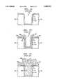
- a substrate useful in forming a layered semiconductor deviceis shown wherein a first conductive layer 10 has an insulator layer 20 formed thereon.
- Insulator layer 20can be made from any typical and well-known dielectric material used in wafer fabrication, but is preferably PETEOS.SiO 2 .
- a contact hole 25 extending down to the first conductive layer 10is formed in insulator layer 20 using known photolithographic techniques. Since the contact hole extends down to a conductive layer, it will be appreciated by those skilled in the art that the structure shown in FIGS. 3A-D is used to form a tungsten plug at the via level. It should be understood, however, that tungsten plugs can also be formed at the window level using the methods disclosed herein.
- Titanium film 30is deposited on the exposed surfaces. Titanium film 30 can be applied, for example, using a vacuum deposition technique, e.g., sputtering (with or without collimation). The thickness of titanium film can be in the range of about 50 ⁇ to about 750 ⁇ , preferably 500-600 ⁇ .
- TiN film 40is then deposited on all exposed surfaces of titanium film 30.
- Titanium nitride film 40can be formed using any known technique such as a reactive sputtering process (with or without collimation) wherein sputtering is carried out in Ar+N 2 atmosphere using a Ti target.
- the thickness of titanium nitride film 40can be in the range of about 50 ⁇ to about 1500 ⁇ , preferably from 600 ⁇ to about 1200 ⁇ .
- TiN film 40serves as an adhesion layer, facilitating deposition of tungsten onto the substrate.
- RTArapid thermal annealing
- substrates containing titanium nitride layers less than 600 ⁇ thickcan be annealed at 550° C. for 20 seconds.
- RTAtends to cure pinhole defects in the titanium nitride layer, thereby reducing the likelihood of volcano growth during tungsten deposition. It should be understood that annealing is an optional step.
- the TiN surfaceis then optionally passivated by bringing silane (SiH 4 ) gas into contact with the TiN surface.
- silaneSiH 4
- the Ti/TiN coated substrateis placed within a vacuum chamber and silane is introduced into the chamber at a flow rate ranging from 75 to 300 standard cubic centimeters per minute ("SCCM") for anywhere from 25 to 150 seconds.
- SCCMstandard cubic centimeters per minute
- the passivation processproduces a discontinuous monolayer of silicon (not shown) on the titanium nitride layer.
- a nucleation layeris formed by performing WF 6 reduction by SiH 4 at relatively low pressures.
- the flow of silane into the chamberis in the range of 75 to 300 SCCM and the flow of WF 6 into the chamber is in the range 35 to 300 SCCM.
- the ratio of SiH 4 : WF 6 flow ratesis from about 6:1 to 4:1.
- Hydrogen (H 2 ) gasis also introduced into the chamber during nucleation at a rate of from 1000 to 6000 SCCM, preferably from 1500 to 3000 SCCM.
- the duration of the nucleation stepis from 10 to 150 seconds at pressure ranging from 0.1 to 1.0 Torr.
- the temperature is during nucleationshould be maintained between about 400°-450° C., preferably 420°-430° C.
- the nucleation stepis believed to provide a WSi x seed layer 50 on the passivated TiN surface (See FIG. 3A). While seed layer 50 is shown in FIG. 3A as a continuous layer, it should be understood that seed layer 50 can be a discontinuous layer applied to the TiN adhesion layer 40.
- the thickness of seed layer 50is up to 30 ⁇ , more preferably 2.5 ⁇ to 25 ⁇ .
- SiH 4 and WF 6are then sequentially shut off and argon (Ar) and Hydrogen (H 2 ) gas are introduced into the chamber at flow rates of about 50 to about 1000 SCCM and about 3000 to about 4000 SCCM, respectively.
- Rapid deposition of tungstenis then achieved by WF 6 reduction with H 2 at a relatively high total pressure.
- the flow of Aris stopped, H 2 is introduced into the chamber at flow rates of from 6000 to 7500 SCCM, preferably 6500 to 7000 SCCM, and WF 6 is introduced into the chamber at flow rates of 300 to 500 SCCM, preferably, about 400 SCCM.
- the total pressure during this deposition stepis in the range 10 Torr to 100 Torr, preferably 20-50 Torr, most preferably 25-35 Torr.
- a flow rate of 400 SCCM for WF 6 and 3800 SCCM for H 2 at a total pressure of 30 torrwill provide a deposition rate of about 50 ⁇ /sec.
- each growth phasewill last for 10 seconds to 2 minutes, preferably 20 second to 1 minute, with intervening periods of no growth of the same or different duration as the growth phase.
- the flow of WF 6is shut off and deposition of the first layer 60A is complete, as shown in FIG. 3B.
- the flow of H 2is reduced to about 3000 to about 4000 SCCM, preferably about 3500 and Ar is added for about one minute.
- Deposition of a second layer 60B (See FIG. 3C) of tungstenis then achieved by WF 6 reduction with H 2 at conditions which provide a relatively slow rate of deposition.
- the flow of Aris stopped and H 2 and WF 6 are introduced into the chamber in the same ratio used in depositing the previous layer, but at slower flow rates.
- flow rates of from 3000 to 5000 SCCM, preferably 3250 to 3500 SCCMare used.
- WF 6is introduced at flow rates of 100 to 300 SCCM, preferably 150 to 250 SCCM.
- the total pressure during this deposition stepis in the range of 10 Torr to 100 Torr, preferably 20-50 Torr, most preferably 25-35 Torr.
- a deposition rate of about 36 ⁇ /sec.is obtained.
- the flow of WF 6is then stopped to end the second growth phase.
- the flow of H 2is continued and Ar is added.
- the conditions for no growthare maintained for anywhere from 10 seconds to 2 minutes, preferably from 30 seconds to 1 minute.
- Tungsten depositionis continued in sequential alternating fast and slow growth phases for a number of times sufficient to substantially fill the contact hole.
- the interrupted tungsten depositionis continued until at least five and preferably seven layers 60 C-G are produced and the contact hole is completely filled with a layered tungsten plug as shown in FIG. 3D.
- the seed layer 50may no longer be noticeable. While not wishing to be bound to any theory, it is believed that the WSi x seed layer is converted to metallic tungsten during the H 2 reduction.
Landscapes
- Engineering & Computer Science (AREA)
- Physics & Mathematics (AREA)
- Condensed Matter Physics & Semiconductors (AREA)
- General Physics & Mathematics (AREA)
- Computer Hardware Design (AREA)
- Microelectronics & Electronic Packaging (AREA)
- Power Engineering (AREA)
- Manufacturing & Machinery (AREA)
- Chemical & Material Sciences (AREA)
- Chemical Kinetics & Catalysis (AREA)
- General Chemical & Material Sciences (AREA)
- Internal Circuitry In Semiconductor Integrated Circuit Devices (AREA)
- Coating By Spraying Or Casting (AREA)
- Other Surface Treatments For Metallic Materials (AREA)
- Electrodes Of Semiconductors (AREA)
- Physical Deposition Of Substances That Are Components Of Semiconductor Devices (AREA)
- Chemical Vapour Deposition (AREA)
Abstract
Description
Claims (18)
Priority Applications (5)
| Application Number | Priority Date | Filing Date | Title |
|---|---|---|---|
| US08/366,529US5489552A (en) | 1994-12-30 | 1994-12-30 | Multiple layer tungsten deposition process |
| TW084108935ATW344893B (en) | 1994-12-30 | 1995-08-28 | Novel tungsten deposition process |
| EP95309093AEP0720211A3 (en) | 1994-12-30 | 1995-12-13 | Novel tungsten deposition process |
| JP7340327AJPH08232079A (en) | 1994-12-30 | 1995-12-27 | New tungsten welding process |
| KR1019950067127AKR960026257A (en) | 1994-12-30 | 1995-12-29 | Multi-Layered Tungsten Deposition Method |
Applications Claiming Priority (1)
| Application Number | Priority Date | Filing Date | Title |
|---|---|---|---|
| US08/366,529US5489552A (en) | 1994-12-30 | 1994-12-30 | Multiple layer tungsten deposition process |
Publications (1)
| Publication Number | Publication Date |
|---|---|
| US5489552Atrue US5489552A (en) | 1996-02-06 |
Family
ID=23443406
Family Applications (1)
| Application Number | Title | Priority Date | Filing Date |
|---|---|---|---|
| US08/366,529Expired - LifetimeUS5489552A (en) | 1994-12-30 | 1994-12-30 | Multiple layer tungsten deposition process |
Country Status (5)
| Country | Link |
|---|---|
| US (1) | US5489552A (en) |
| EP (1) | EP0720211A3 (en) |
| JP (1) | JPH08232079A (en) |
| KR (1) | KR960026257A (en) |
| TW (1) | TW344893B (en) |
Cited By (50)
| Publication number | Priority date | Publication date | Assignee | Title |
|---|---|---|---|---|
| US5643632A (en)* | 1995-10-13 | 1997-07-01 | Mosel Vitelic, Inc. | Tungsten chemical vapor deposition process for suppression of volcano formation |
| US5656545A (en)* | 1996-02-26 | 1997-08-12 | Taiwan Semiconductor Manufacturing Company, Ltd | Elimination of tungsten dimple for stacked contact or via application |
| US5661080A (en)* | 1992-12-10 | 1997-08-26 | Hyundai Electronics Industries Co., Ltd. | Method for fabricating tungsten plug |
| US5672543A (en)* | 1996-04-29 | 1997-09-30 | Taiwan Semiconductor Manufacturing Company, Ltd. | Volcano defect-free tungsten plug |
| US5700726A (en)* | 1996-06-21 | 1997-12-23 | Taiwan Semiconductor Manufacturing Company Ltd | Multi-layered tungsten depositions for contact hole filling |
| US5804249A (en)* | 1997-02-07 | 1998-09-08 | Lsi Logic Corporation | Multistep tungsten CVD process with amorphization step |
| US5913146A (en)* | 1997-03-18 | 1999-06-15 | Lucent Technologies Inc. | Semiconductor device having aluminum contacts or vias and method of manufacture therefor |
| US5956609A (en)* | 1997-08-11 | 1999-09-21 | Taiwan Semiconductor Manufacturing Company, Ltd. | Method for reducing stress and improving step-coverage of tungsten interconnects and plugs |
| US6017818A (en)* | 1996-01-22 | 2000-01-25 | Texas Instruments Incorporated | Process for fabricating conformal Ti-Si-N and Ti-B-N based barrier films with low defect density |
| EP1055746A1 (en)* | 1999-05-24 | 2000-11-29 | Lucent Technologies Inc. | Method of chemical vapor depositing tungsten films |
| US6287964B1 (en)* | 1998-01-26 | 2001-09-11 | Hyundai Electronics Industries Co., Ltd. | Method for forming a metallization layer of a semiconductor device |
| US6309966B1 (en)* | 1999-09-03 | 2001-10-30 | Motorola, Inc. | Apparatus and method of a low pressure, two-step nucleation tungsten deposition |
| US6316132B1 (en)* | 1999-09-02 | 2001-11-13 | Xilinx, Inc. | Structure and method for preventing barrier failure |
| US6358844B1 (en)* | 2000-06-01 | 2002-03-19 | Taiwan Semiconductor Manufacturing, Company, Ltd | Tungsten deposition process with dual-step nucleation |
| US20020053734A1 (en)* | 1993-11-16 | 2002-05-09 | Formfactor, Inc. | Probe card assembly and kit, and methods of making same |
| US6387445B1 (en)* | 1999-01-13 | 2002-05-14 | Tokyo Electron Limited | Tungsten layer forming method and laminate structure of tungsten layer |
| US6472309B1 (en) | 1998-02-13 | 2002-10-29 | Micron Technology, Inc. | In situ plasma pre-deposition wafer treatment in chemical vapor deposition technology for semiconductor integrated circuit applications |
| US6489239B1 (en) | 1999-12-06 | 2002-12-03 | Samsung Electronics Co., Ltd. | Method of tungsten chemical vapor deposition and tungsten plug formation |
| US20030082902A1 (en)* | 2001-10-31 | 2003-05-01 | Shoichi Fukui | Semiconductor-device fabrication method |
| US6569699B1 (en)* | 2000-02-01 | 2003-05-27 | Chartered Semiconductor Manufacturing Ltd. | Two layer mirror for LCD-on-silicon products and method of fabrication thereof |
| US6593233B1 (en)* | 1995-03-03 | 2003-07-15 | Nec Electronics Corporation | Semiconductor device and method for manufacturing the same |
| US20030170981A1 (en)* | 2000-07-28 | 2003-09-11 | Hotaka Ishizuka | Method for forming film |
| US20030199179A1 (en)* | 1993-11-16 | 2003-10-23 | Formfactor, Inc. | Contact tip structure for microelectronic interconnection elements and method of making same |
| US20040224501A1 (en)* | 1996-05-22 | 2004-11-11 | Yung-Tsun Lo | Manufacturing method for making tungsten-plug in an intergrated circuit device without volcano phenomena |
| US6982226B1 (en) | 1998-06-05 | 2006-01-03 | Agere Systems Inc. | Method of fabricating a contact with a post contact plug anneal |
| US20080265423A1 (en)* | 2007-04-27 | 2008-10-30 | Ruben David A | Layered structure for corrosion resistant interconnect contacts |
| US7601039B2 (en) | 1993-11-16 | 2009-10-13 | Formfactor, Inc. | Microelectronic contact structure and method of making same |
| US20110163449A1 (en)* | 2010-01-07 | 2011-07-07 | International Business Machines Corporation | Superfilled metal contact vias for semiconductor devices |
| US8033838B2 (en) | 1996-02-21 | 2011-10-11 | Formfactor, Inc. | Microelectronic contact structure |
| US9034768B2 (en) | 2010-07-09 | 2015-05-19 | Novellus Systems, Inc. | Depositing tungsten into high aspect ratio features |
| US9082826B2 (en) | 2013-05-24 | 2015-07-14 | Lam Research Corporation | Methods and apparatuses for void-free tungsten fill in three-dimensional semiconductor features |
| US9240347B2 (en) | 2012-03-27 | 2016-01-19 | Novellus Systems, Inc. | Tungsten feature fill |
| US9349637B2 (en) | 2014-08-21 | 2016-05-24 | Lam Research Corporation | Method for void-free cobalt gap fill |
| US9548228B2 (en) | 2009-08-04 | 2017-01-17 | Lam Research Corporation | Void free tungsten fill in different sized features |
| US9589835B2 (en) | 2008-12-10 | 2017-03-07 | Novellus Systems, Inc. | Method for forming tungsten film having low resistivity, low roughness and high reflectivity |
| US9748137B2 (en) | 2014-08-21 | 2017-08-29 | Lam Research Corporation | Method for void-free cobalt gap fill |
| US20170309490A1 (en)* | 2014-09-24 | 2017-10-26 | Hitachi Kokusai Electric Inc. | Method of manufacturing semiconductor device |
| US9972504B2 (en) | 2015-08-07 | 2018-05-15 | Lam Research Corporation | Atomic layer etching of tungsten for enhanced tungsten deposition fill |
| US9978610B2 (en) | 2015-08-21 | 2018-05-22 | Lam Research Corporation | Pulsing RF power in etch process to enhance tungsten gapfill performance |
| US9997405B2 (en) | 2014-09-30 | 2018-06-12 | Lam Research Corporation | Feature fill with nucleation inhibition |
| US10170320B2 (en) | 2015-05-18 | 2019-01-01 | Lam Research Corporation | Feature fill with multi-stage nucleation inhibition |
| US10211099B2 (en) | 2016-12-19 | 2019-02-19 | Lam Research Corporation | Chamber conditioning for remote plasma process |
| US10256142B2 (en) | 2009-08-04 | 2019-04-09 | Novellus Systems, Inc. | Tungsten feature fill with nucleation inhibition |
| US10381266B2 (en) | 2012-03-27 | 2019-08-13 | Novellus Systems, Inc. | Tungsten feature fill with nucleation inhibition |
| US10566211B2 (en) | 2016-08-30 | 2020-02-18 | Lam Research Corporation | Continuous and pulsed RF plasma for etching metals |
| US10573522B2 (en) | 2016-08-16 | 2020-02-25 | Lam Research Corporation | Method for preventing line bending during metal fill process |
| CN113053804A (en)* | 2021-03-10 | 2021-06-29 | 中国科学院微电子研究所 | Tungsten composite film layer, growth method thereof and monolithic 3DIC |
| US11437269B2 (en) | 2012-03-27 | 2022-09-06 | Novellus Systems, Inc. | Tungsten feature fill with nucleation inhibition |
| CN115910917A (en)* | 2023-01-05 | 2023-04-04 | 广州粤芯半导体技术有限公司 | Metal tungsten film and preparation method thereof |
| US11978666B2 (en) | 2018-12-05 | 2024-05-07 | Lam Research Corporation | Void free low stress fill |
Families Citing this family (1)
| Publication number | Priority date | Publication date | Assignee | Title |
|---|---|---|---|---|
| US5843625A (en)* | 1996-07-23 | 1998-12-01 | Advanced Micro Devices, Inc. | Method of reducing via and contact dimensions beyond photolithography equipment limits |
Citations (24)
| Publication number | Priority date | Publication date | Assignee | Title |
|---|---|---|---|---|
| US4532702A (en)* | 1983-11-04 | 1985-08-06 | Westinghouse Electric Corp. | Method of forming conductive interconnection between vertically spaced levels in VLSI devices |
| US4629635A (en)* | 1984-03-16 | 1986-12-16 | Genus, Inc. | Process for depositing a low resistivity tungsten silicon composite film on a substrate |
| US4804560A (en)* | 1986-03-17 | 1989-02-14 | Fujitsu Limited | Method of selectively depositing tungsten upon a semiconductor substrate |
| JPH01160011A (en)* | 1987-12-17 | 1989-06-22 | Fujitsu Ltd | Manufacture of semiconductor device |
| US4849260A (en)* | 1986-06-30 | 1989-07-18 | Nihon Sinku Gijutsu Kabushiki Kaisha | Method for selectively depositing metal on a substrate |
| US4874719A (en)* | 1986-05-06 | 1989-10-17 | Kabushiki Kaisha Toshiba | Method for manufacturing an electrical connection between conductor levels |
| JPH02199827A (en)* | 1989-01-30 | 1990-08-08 | Hitachi Ltd | Fine wiring |
| US4985371A (en)* | 1988-12-09 | 1991-01-15 | At&T Bell Laboratories | Process for making integrated-circuit device metallization |
| JPH0360126A (en)* | 1989-07-28 | 1991-03-15 | Toshiba Corp | Manufacture of semiconductor device |
| US5108952A (en)* | 1988-08-22 | 1992-04-28 | Oki Electric Industry Co., Ltd. | Method of depositing a tungsten film |
| US5143861A (en)* | 1989-03-06 | 1992-09-01 | Sgs-Thomson Microelectronics, Inc. | Method making a dynamic random access memory cell with a tungsten plug |
| US5164330A (en)* | 1991-04-17 | 1992-11-17 | Intel Corporation | Etchback process for tungsten utilizing a NF3/AR chemistry |
| JPH053170A (en)* | 1991-06-24 | 1993-01-08 | Sony Corp | Forming method of blanket tungsten plug |
| US5183782A (en)* | 1991-01-26 | 1993-02-02 | Sharp Kabushiki Kaisha | Process for fabricating a semiconductor device including a tungsten silicide adhesive layer |
| US5200360A (en)* | 1991-11-12 | 1993-04-06 | Hewlett-Packard Company | Method for reducing selectivity loss in selective tungsten deposition |
| US5202579A (en)* | 1991-01-30 | 1993-04-13 | Mitsubishi Denki Kabushiki Kaisha | Semiconductor device having multilayer interconnection structure |
| JPH05152292A (en)* | 1991-11-30 | 1993-06-18 | Sony Corp | Wiring formation |
| US5233223A (en)* | 1989-01-09 | 1993-08-03 | Nec Corporation | Semiconductor device having a plurality of conductive layers interconnected via a tungsten plug |
| US5232873A (en)* | 1992-10-13 | 1993-08-03 | At&T Bell Laboratories | Method of fabricating contacts for semiconductor devices |
| US5244534A (en)* | 1992-01-24 | 1993-09-14 | Micron Technology, Inc. | Two-step chemical mechanical polishing process for producing flush and protruding tungsten plugs |
| US5260232A (en)* | 1991-04-05 | 1993-11-09 | Sony Corporation | Refractory metal plug forming method |
| US5272112A (en)* | 1992-11-09 | 1993-12-21 | Genus, Inc. | Low-temperature low-stress blanket tungsten film |
| US5327011A (en)* | 1991-07-23 | 1994-07-05 | Seiko Epson Corporation | Semiconductor device with enhanced via or contact hole connection between an interconnect layer and a connecting region |
| US5407698A (en)* | 1992-04-29 | 1995-04-18 | Northern Telecom Limited | Deposition of tungsten |
Family Cites Families (3)
| Publication number | Priority date | Publication date | Assignee | Title |
|---|---|---|---|---|
| KR930000309B1 (en)* | 1989-11-22 | 1993-01-15 | 삼성전자 주식회사 | Manufacturing method of semiconductor device |
| JPH04363024A (en)* | 1990-11-30 | 1992-12-15 | Toshiba Corp | Manufacture of semiconductor device |
| GB9219281D0 (en)* | 1992-09-11 | 1992-10-28 | Inmos Ltd | Manufacture of semiconductor devices |
- 1994
- 1994-12-30USUS08/366,529patent/US5489552A/ennot_activeExpired - Lifetime
- 1995
- 1995-08-28TWTW084108935Apatent/TW344893B/enactive
- 1995-12-13EPEP95309093Apatent/EP0720211A3/ennot_activeWithdrawn
- 1995-12-27JPJP7340327Apatent/JPH08232079A/ennot_activeWithdrawn
- 1995-12-29KRKR1019950067127Apatent/KR960026257A/ennot_activeCeased
Patent Citations (25)
| Publication number | Priority date | Publication date | Assignee | Title |
|---|---|---|---|---|
| US4532702A (en)* | 1983-11-04 | 1985-08-06 | Westinghouse Electric Corp. | Method of forming conductive interconnection between vertically spaced levels in VLSI devices |
| US4629635A (en)* | 1984-03-16 | 1986-12-16 | Genus, Inc. | Process for depositing a low resistivity tungsten silicon composite film on a substrate |
| US4804560A (en)* | 1986-03-17 | 1989-02-14 | Fujitsu Limited | Method of selectively depositing tungsten upon a semiconductor substrate |
| US4874719A (en)* | 1986-05-06 | 1989-10-17 | Kabushiki Kaisha Toshiba | Method for manufacturing an electrical connection between conductor levels |
| US4849260A (en)* | 1986-06-30 | 1989-07-18 | Nihon Sinku Gijutsu Kabushiki Kaisha | Method for selectively depositing metal on a substrate |
| JPH01160011A (en)* | 1987-12-17 | 1989-06-22 | Fujitsu Ltd | Manufacture of semiconductor device |
| US5108952A (en)* | 1988-08-22 | 1992-04-28 | Oki Electric Industry Co., Ltd. | Method of depositing a tungsten film |
| US4985371A (en)* | 1988-12-09 | 1991-01-15 | At&T Bell Laboratories | Process for making integrated-circuit device metallization |
| US5233223A (en)* | 1989-01-09 | 1993-08-03 | Nec Corporation | Semiconductor device having a plurality of conductive layers interconnected via a tungsten plug |
| JPH02199827A (en)* | 1989-01-30 | 1990-08-08 | Hitachi Ltd | Fine wiring |
| US5143861A (en)* | 1989-03-06 | 1992-09-01 | Sgs-Thomson Microelectronics, Inc. | Method making a dynamic random access memory cell with a tungsten plug |
| JPH0360126A (en)* | 1989-07-28 | 1991-03-15 | Toshiba Corp | Manufacture of semiconductor device |
| US5183782A (en)* | 1991-01-26 | 1993-02-02 | Sharp Kabushiki Kaisha | Process for fabricating a semiconductor device including a tungsten silicide adhesive layer |
| US5312775A (en)* | 1991-01-30 | 1994-05-17 | Mitsubishi Denki Kabushiki Kaisha | Method of manufacturing semiconductor device having multilayer interconnection structure |
| US5202579A (en)* | 1991-01-30 | 1993-04-13 | Mitsubishi Denki Kabushiki Kaisha | Semiconductor device having multilayer interconnection structure |
| US5260232A (en)* | 1991-04-05 | 1993-11-09 | Sony Corporation | Refractory metal plug forming method |
| US5164330A (en)* | 1991-04-17 | 1992-11-17 | Intel Corporation | Etchback process for tungsten utilizing a NF3/AR chemistry |
| JPH053170A (en)* | 1991-06-24 | 1993-01-08 | Sony Corp | Forming method of blanket tungsten plug |
| US5327011A (en)* | 1991-07-23 | 1994-07-05 | Seiko Epson Corporation | Semiconductor device with enhanced via or contact hole connection between an interconnect layer and a connecting region |
| US5200360A (en)* | 1991-11-12 | 1993-04-06 | Hewlett-Packard Company | Method for reducing selectivity loss in selective tungsten deposition |
| JPH05152292A (en)* | 1991-11-30 | 1993-06-18 | Sony Corp | Wiring formation |
| US5244534A (en)* | 1992-01-24 | 1993-09-14 | Micron Technology, Inc. | Two-step chemical mechanical polishing process for producing flush and protruding tungsten plugs |
| US5407698A (en)* | 1992-04-29 | 1995-04-18 | Northern Telecom Limited | Deposition of tungsten |
| US5232873A (en)* | 1992-10-13 | 1993-08-03 | At&T Bell Laboratories | Method of fabricating contacts for semiconductor devices |
| US5272112A (en)* | 1992-11-09 | 1993-12-21 | Genus, Inc. | Low-temperature low-stress blanket tungsten film |
Non-Patent Citations (2)
| Title |
|---|
| "High Pressure Blanket CVD Tungsten", Thomas Clark et al., Mat. Res. Soc. Symp. Proc. VLSI V, 1990 Material Research Society. |
| High Pressure Blanket CVD Tungsten , Thomas Clark et al., Mat. Res. Soc. Symp. Proc. VLSI V, 1990 Material Research Society.* |
Cited By (78)
| Publication number | Priority date | Publication date | Assignee | Title |
|---|---|---|---|---|
| US5661080A (en)* | 1992-12-10 | 1997-08-26 | Hyundai Electronics Industries Co., Ltd. | Method for fabricating tungsten plug |
| US7601039B2 (en) | 1993-11-16 | 2009-10-13 | Formfactor, Inc. | Microelectronic contact structure and method of making same |
| US8373428B2 (en) | 1993-11-16 | 2013-02-12 | Formfactor, Inc. | Probe card assembly and kit, and methods of making same |
| US20020053734A1 (en)* | 1993-11-16 | 2002-05-09 | Formfactor, Inc. | Probe card assembly and kit, and methods of making same |
| US20030199179A1 (en)* | 1993-11-16 | 2003-10-23 | Formfactor, Inc. | Contact tip structure for microelectronic interconnection elements and method of making same |
| US6593233B1 (en)* | 1995-03-03 | 2003-07-15 | Nec Electronics Corporation | Semiconductor device and method for manufacturing the same |
| US5643632A (en)* | 1995-10-13 | 1997-07-01 | Mosel Vitelic, Inc. | Tungsten chemical vapor deposition process for suppression of volcano formation |
| US6017818A (en)* | 1996-01-22 | 2000-01-25 | Texas Instruments Incorporated | Process for fabricating conformal Ti-Si-N and Ti-B-N based barrier films with low defect density |
| US8033838B2 (en) | 1996-02-21 | 2011-10-11 | Formfactor, Inc. | Microelectronic contact structure |
| US5656545A (en)* | 1996-02-26 | 1997-08-12 | Taiwan Semiconductor Manufacturing Company, Ltd | Elimination of tungsten dimple for stacked contact or via application |
| US5672543A (en)* | 1996-04-29 | 1997-09-30 | Taiwan Semiconductor Manufacturing Company, Ltd. | Volcano defect-free tungsten plug |
| US20040224501A1 (en)* | 1996-05-22 | 2004-11-11 | Yung-Tsun Lo | Manufacturing method for making tungsten-plug in an intergrated circuit device without volcano phenomena |
| US5700726A (en)* | 1996-06-21 | 1997-12-23 | Taiwan Semiconductor Manufacturing Company Ltd | Multi-layered tungsten depositions for contact hole filling |
| US6016009A (en)* | 1997-02-07 | 2000-01-18 | Lsi Logic Corporation | Integrated circuit with tungsten plug containing amorphization layer |
| US5804249A (en)* | 1997-02-07 | 1998-09-08 | Lsi Logic Corporation | Multistep tungsten CVD process with amorphization step |
| US5913146A (en)* | 1997-03-18 | 1999-06-15 | Lucent Technologies Inc. | Semiconductor device having aluminum contacts or vias and method of manufacture therefor |
| US6157082A (en)* | 1997-03-18 | 2000-12-05 | Lucent Technologies Inc. | Semiconductor device having aluminum contacts or vias and method of manufacture therefor |
| US5956609A (en)* | 1997-08-11 | 1999-09-21 | Taiwan Semiconductor Manufacturing Company, Ltd. | Method for reducing stress and improving step-coverage of tungsten interconnects and plugs |
| US6287964B1 (en)* | 1998-01-26 | 2001-09-11 | Hyundai Electronics Industries Co., Ltd. | Method for forming a metallization layer of a semiconductor device |
| US7186638B2 (en) | 1998-02-13 | 2007-03-06 | Micron Technology, Inc. | Passivation processes for use with metallization techniques |
| US6472309B1 (en) | 1998-02-13 | 2002-10-29 | Micron Technology, Inc. | In situ plasma pre-deposition wafer treatment in chemical vapor deposition technology for semiconductor integrated circuit applications |
| US20050032367A1 (en)* | 1998-02-13 | 2005-02-10 | Weimin Li | Passivation processes for use with metallization techniques |
| US6503822B2 (en) | 1998-02-13 | 2003-01-07 | Micron Technology, Inc. | Methods for insitu plasma pre-deposition wafer treatment in chemical vapor deposition technology for semiconductor integrated circuit applications |
| US6515363B2 (en)* | 1998-02-13 | 2003-02-04 | Micron Technology, Inc. | In situ plasma pre-deposition wafer treatment in chemical vapor deposition technology for semiconductor integrated circuit applications |
| US6815819B2 (en) | 1998-02-13 | 2004-11-09 | Micron Technology, Inc. | In situ plasma pre-deposition wafer treatment in chemical vapor deposition technology for semiconductor integrated circuit applications |
| US6982226B1 (en) | 1998-06-05 | 2006-01-03 | Agere Systems Inc. | Method of fabricating a contact with a post contact plug anneal |
| US6387445B1 (en)* | 1999-01-13 | 2002-05-14 | Tokyo Electron Limited | Tungsten layer forming method and laminate structure of tungsten layer |
| EP1055746A1 (en)* | 1999-05-24 | 2000-11-29 | Lucent Technologies Inc. | Method of chemical vapor depositing tungsten films |
| US6294468B1 (en) | 1999-05-24 | 2001-09-25 | Agere Systems Guardian Corp. | Method of chemical vapor depositing tungsten films |
| US6638852B1 (en) | 1999-09-02 | 2003-10-28 | Xilinx, Inc. | Structure and method for preventing barrier failure |
| US6316132B1 (en)* | 1999-09-02 | 2001-11-13 | Xilinx, Inc. | Structure and method for preventing barrier failure |
| US6309966B1 (en)* | 1999-09-03 | 2001-10-30 | Motorola, Inc. | Apparatus and method of a low pressure, two-step nucleation tungsten deposition |
| US6489239B1 (en) | 1999-12-06 | 2002-12-03 | Samsung Electronics Co., Ltd. | Method of tungsten chemical vapor deposition and tungsten plug formation |
| US6569699B1 (en)* | 2000-02-01 | 2003-05-27 | Chartered Semiconductor Manufacturing Ltd. | Two layer mirror for LCD-on-silicon products and method of fabrication thereof |
| US6822268B2 (en)* | 2000-02-01 | 2004-11-23 | Chartered Semiconductor Manufacturing Ltd. | Two layer mirror for LCD-on-silicon products and method of fabrication thereof |
| US20030203526A1 (en)* | 2000-02-01 | 2003-10-30 | Chartered Semiconductor Manufacturing Ltd. | Two layer mirror for LCD-on -silicon products and method of fabrication thereof |
| US6358844B1 (en)* | 2000-06-01 | 2002-03-19 | Taiwan Semiconductor Manufacturing, Company, Ltd | Tungsten deposition process with dual-step nucleation |
| US7060614B2 (en) | 2000-07-28 | 2006-06-13 | Tokyo Electron Limited | Method for forming film |
| US20030170981A1 (en)* | 2000-07-28 | 2003-09-11 | Hotaka Ishizuka | Method for forming film |
| US20030082902A1 (en)* | 2001-10-31 | 2003-05-01 | Shoichi Fukui | Semiconductor-device fabrication method |
| US6683000B2 (en)* | 2001-10-31 | 2004-01-27 | Mitsubishi Denki Kabushiki Kaisha | Semiconductor-device fabrication method |
| US20080265423A1 (en)* | 2007-04-27 | 2008-10-30 | Ruben David A | Layered structure for corrosion resistant interconnect contacts |
| US8461681B2 (en)* | 2007-04-27 | 2013-06-11 | Medtronic, Inc. | Layered structure for corrosion resistant interconnect contacts |
| US9589835B2 (en) | 2008-12-10 | 2017-03-07 | Novellus Systems, Inc. | Method for forming tungsten film having low resistivity, low roughness and high reflectivity |
| US9548228B2 (en) | 2009-08-04 | 2017-01-17 | Lam Research Corporation | Void free tungsten fill in different sized features |
| US10103058B2 (en) | 2009-08-04 | 2018-10-16 | Novellus Systems, Inc. | Tungsten feature fill |
| US9653353B2 (en) | 2009-08-04 | 2017-05-16 | Novellus Systems, Inc. | Tungsten feature fill |
| US11075115B2 (en) | 2009-08-04 | 2021-07-27 | Novellus Systems, Inc. | Tungsten feature fill |
| US10256142B2 (en) | 2009-08-04 | 2019-04-09 | Novellus Systems, Inc. | Tungsten feature fill with nucleation inhibition |
| US8691687B2 (en) | 2010-01-07 | 2014-04-08 | International Business Machines Corporation | Superfilled metal contact vias for semiconductor devices |
| US20110163449A1 (en)* | 2010-01-07 | 2011-07-07 | International Business Machines Corporation | Superfilled metal contact vias for semiconductor devices |
| US8698318B2 (en) | 2010-01-07 | 2014-04-15 | International Business Machines Corporation | Superfilled metal contact vias for semiconductor devices |
| US9034768B2 (en) | 2010-07-09 | 2015-05-19 | Novellus Systems, Inc. | Depositing tungsten into high aspect ratio features |
| US9240347B2 (en) | 2012-03-27 | 2016-01-19 | Novellus Systems, Inc. | Tungsten feature fill |
| US11437269B2 (en) | 2012-03-27 | 2022-09-06 | Novellus Systems, Inc. | Tungsten feature fill with nucleation inhibition |
| US10381266B2 (en) | 2012-03-27 | 2019-08-13 | Novellus Systems, Inc. | Tungsten feature fill with nucleation inhibition |
| US9082826B2 (en) | 2013-05-24 | 2015-07-14 | Lam Research Corporation | Methods and apparatuses for void-free tungsten fill in three-dimensional semiconductor features |
| US9748137B2 (en) | 2014-08-21 | 2017-08-29 | Lam Research Corporation | Method for void-free cobalt gap fill |
| US9349637B2 (en) | 2014-08-21 | 2016-05-24 | Lam Research Corporation | Method for void-free cobalt gap fill |
| US20170309490A1 (en)* | 2014-09-24 | 2017-10-26 | Hitachi Kokusai Electric Inc. | Method of manufacturing semiconductor device |
| US10580695B2 (en) | 2014-09-30 | 2020-03-03 | Lam Research Corporation | Feature fill with nucleation inhibition |
| US11901227B2 (en) | 2014-09-30 | 2024-02-13 | Lam Research Corporation | Feature fill with nucleation inhibition |
| US9997405B2 (en) | 2014-09-30 | 2018-06-12 | Lam Research Corporation | Feature fill with nucleation inhibition |
| US10916434B2 (en) | 2015-05-18 | 2021-02-09 | Lam Research Corporation | Feature fill with multi-stage nucleation inhibition |
| US10580654B2 (en) | 2015-05-18 | 2020-03-03 | Lam Research Corporation | Feature fill with multi-stage nucleation inhibition |
| US10170320B2 (en) | 2015-05-18 | 2019-01-01 | Lam Research Corporation | Feature fill with multi-stage nucleation inhibition |
| US11069535B2 (en) | 2015-08-07 | 2021-07-20 | Lam Research Corporation | Atomic layer etch of tungsten for enhanced tungsten deposition fill |
| US9972504B2 (en) | 2015-08-07 | 2018-05-15 | Lam Research Corporation | Atomic layer etching of tungsten for enhanced tungsten deposition fill |
| US10395944B2 (en) | 2015-08-21 | 2019-08-27 | Lam Research Corporation | Pulsing RF power in etch process to enhance tungsten gapfill performance |
| US9978610B2 (en) | 2015-08-21 | 2018-05-22 | Lam Research Corporation | Pulsing RF power in etch process to enhance tungsten gapfill performance |
| US11355345B2 (en) | 2016-08-16 | 2022-06-07 | Lam Research Corporation | Method for preventing line bending during metal fill process |
| US10573522B2 (en) | 2016-08-16 | 2020-02-25 | Lam Research Corporation | Method for preventing line bending during metal fill process |
| US10566211B2 (en) | 2016-08-30 | 2020-02-18 | Lam Research Corporation | Continuous and pulsed RF plasma for etching metals |
| US10211099B2 (en) | 2016-12-19 | 2019-02-19 | Lam Research Corporation | Chamber conditioning for remote plasma process |
| US11978666B2 (en) | 2018-12-05 | 2024-05-07 | Lam Research Corporation | Void free low stress fill |
| CN113053804A (en)* | 2021-03-10 | 2021-06-29 | 中国科学院微电子研究所 | Tungsten composite film layer, growth method thereof and monolithic 3DIC |
| CN113053804B (en)* | 2021-03-10 | 2023-02-21 | 中国科学院微电子研究所 | A kind of tungsten composite film layer and its growth method, monolithic 3DIC |
| CN115910917A (en)* | 2023-01-05 | 2023-04-04 | 广州粤芯半导体技术有限公司 | Metal tungsten film and preparation method thereof |
Also Published As
| Publication number | Publication date |
|---|---|
| TW344893B (en) | 1998-11-11 |
| EP0720211A3 (en) | 1997-03-05 |
| JPH08232079A (en) | 1996-09-10 |
| EP0720211A2 (en) | 1996-07-03 |
| KR960026257A (en) | 1996-07-22 |
Similar Documents
| Publication | Publication Date | Title |
|---|---|---|
| US5489552A (en) | Multiple layer tungsten deposition process | |
| US5599739A (en) | Barrier layer treatments for tungsten plug | |
| US6291342B2 (en) | Methods of forming titanium nitride composite layers using composite gases having increasing TiCl4 to NH3 ratios | |
| EP1313140A1 (en) | Method of forming a liner for tungsten plugs | |
| JPH11163141A (en) | Manufacture of silicon integrated circuit | |
| JP2889430B2 (en) | Contact part forming method | |
| JPS595629A (en) | Double layer surface stabilizing method | |
| US5804501A (en) | Method for forming a wiring metal layer in a semiconductor device | |
| JPH0936228A (en) | Formation of wiring | |
| EP0740336B1 (en) | Method for fabricating semiconductor device having buried contact structure | |
| US5874360A (en) | Manufacture of semiconductor devices | |
| JP2001308032A (en) | Method and apparatus for depositing low residual halogen-containing TiN films with a thickness greater than 1000 ° | |
| US6022800A (en) | Method of forming barrier layer for tungsten plugs in interlayer dielectrics | |
| US6100182A (en) | Method for forming metal interconnection of semiconductor device | |
| JPH0577290B2 (en) | ||
| JP2733396B2 (en) | Method for manufacturing semiconductor device | |
| JPH053170A (en) | Forming method of blanket tungsten plug | |
| JPH06275555A (en) | Method for manufacturing semiconductor device | |
| US5953631A (en) | Low stress, highly conformal CVD metal thin film | |
| JPH07183250A (en) | Contact formation method | |
| JPH08153783A (en) | Formation of electrically connecting section and manufacture of semiconductor device | |
| JPH08111455A (en) | Wiring formation method | |
| JP2706388B2 (en) | Method for manufacturing semiconductor device | |
| KR100510465B1 (en) | Method for forming barrier metal layer in semiconductor device | |
| JPH0562929A (en) | Method for manufacturing semiconductor device |
Legal Events
| Date | Code | Title | Description |
|---|---|---|---|
| AS | Assignment | Owner name:AT&T IPM CORP., FLORIDA Free format text:ASSIGNMENT OF ASSIGNORS INTEREST;ASSIGNORS:MERCHANT, SAILESH MANSINH;NANDA, ARUN KUMAR;ROY, PRADIP KUMAR;REEL/FRAME:007583/0157;SIGNING DATES FROM 19950324 TO 19950525 | |
| STCF | Information on status: patent grant | Free format text:PATENTED CASE | |
| FEPP | Fee payment procedure | Free format text:PAYOR NUMBER ASSIGNED (ORIGINAL EVENT CODE: ASPN); ENTITY STATUS OF PATENT OWNER: LARGE ENTITY | |
| FPAY | Fee payment | Year of fee payment:4 | |
| AS | Assignment | Owner name:CHASE MANHATTAN BANK, AS ADMINISTRATIVE AGENT, THE Free format text:CONDITIONAL ASSIGNMENT OF AND SECURITY INTEREST IN PATENT RIGHTS;ASSIGNOR:AGERE SYSTEMS GUARDIAN CORP. (DE CORPORATION);REEL/FRAME:011667/0148 Effective date:20010402 | |
| AS | Assignment | Owner name:AGERE SYSTEMS GUARDIAN CORP., FLORIDA Free format text:ASSIGNMENT OF ASSIGNORS INTEREST;ASSIGNOR:LUCENT TECHNOLOGIES INC.;REEL/FRAME:011796/0615 Effective date:20010131 | |
| AS | Assignment | Owner name:AGERE SYSTEMS GUARDIAN CORP., FLORIDA Free format text:TERMINATION AND RELEASE OF SECURITY INTEREST IN PATENT RIGHTS;ASSIGNOR:JPMORGAN CHASE BANK (F/K/A THE CHASE MANHATTAN BANK);REEL/FRAME:013372/0662 Effective date:20020930 | |
| FEPP | Fee payment procedure | Free format text:PAYOR NUMBER ASSIGNED (ORIGINAL EVENT CODE: ASPN); ENTITY STATUS OF PATENT OWNER: LARGE ENTITY Free format text:PAYER NUMBER DE-ASSIGNED (ORIGINAL EVENT CODE: RMPN); ENTITY STATUS OF PATENT OWNER: LARGE ENTITY | |
| FPAY | Fee payment | Year of fee payment:8 | |
| FPAY | Fee payment | Year of fee payment:12 | |
| AS | Assignment | Owner name:DEUTSCHE BANK AG NEW YORK BRANCH, AS COLLATERAL AG Free format text:PATENT SECURITY AGREEMENT;ASSIGNORS:LSI CORPORATION;AGERE SYSTEMS LLC;REEL/FRAME:032856/0031 Effective date:20140506 | |
| AS | Assignment | Owner name:AVAGO TECHNOLOGIES GENERAL IP (SINGAPORE) PTE. LTD Free format text:ASSIGNMENT OF ASSIGNORS INTEREST;ASSIGNOR:AGERE SYSTEMS LLC;REEL/FRAME:035365/0634 Effective date:20140804 | |
| AS | Assignment | Owner name:AGERE SYSTEMS LLC, PENNSYLVANIA Free format text:TERMINATION AND RELEASE OF SECURITY INTEREST IN PATENT RIGHTS (RELEASES RF 032856-0031);ASSIGNOR:DEUTSCHE BANK AG NEW YORK BRANCH, AS COLLATERAL AGENT;REEL/FRAME:037684/0039 Effective date:20160201 Owner name:LSI CORPORATION, CALIFORNIA Free format text:TERMINATION AND RELEASE OF SECURITY INTEREST IN PATENT RIGHTS (RELEASES RF 032856-0031);ASSIGNOR:DEUTSCHE BANK AG NEW YORK BRANCH, AS COLLATERAL AGENT;REEL/FRAME:037684/0039 Effective date:20160201 | |
| AS | Assignment | Owner name:BELL SEMICONDUCTOR, LLC, ILLINOIS Free format text:ASSIGNMENT OF ASSIGNORS INTEREST;ASSIGNORS:AVAGO TECHNOLOGIES GENERAL IP (SINGAPORE) PTE. LTD.;BROADCOM CORPORATION;REEL/FRAME:044886/0001 Effective date:20171208 | |
| AS | Assignment | Owner name:CORTLAND CAPITAL MARKET SERVICES LLC, AS COLLATERA Free format text:SECURITY INTEREST;ASSIGNORS:HILCO PATENT ACQUISITION 56, LLC;BELL SEMICONDUCTOR, LLC;BELL NORTHERN RESEARCH, LLC;REEL/FRAME:045216/0020 Effective date:20180124 | |
| AS | Assignment | Owner name:BELL NORTHERN RESEARCH, LLC, ILLINOIS Free format text:SECURITY INTEREST;ASSIGNOR:CORTLAND CAPITAL MARKET SERVICES LLC;REEL/FRAME:060885/0001 Effective date:20220401 Owner name:BELL SEMICONDUCTOR, LLC, ILLINOIS Free format text:SECURITY INTEREST;ASSIGNOR:CORTLAND CAPITAL MARKET SERVICES LLC;REEL/FRAME:060885/0001 Effective date:20220401 Owner name:HILCO PATENT ACQUISITION 56, LLC, ILLINOIS Free format text:SECURITY INTEREST;ASSIGNOR:CORTLAND CAPITAL MARKET SERVICES LLC;REEL/FRAME:060885/0001 Effective date:20220401 |