US5488693A - Protocol with control bits and bytes for controlling the order of communications between a master processor and plural slave processors - Google Patents
Protocol with control bits and bytes for controlling the order of communications between a master processor and plural slave processorsDownload PDFInfo
- Publication number
- US5488693A US5488693AUS07/903,304US90330492AUS5488693AUS 5488693 AUS5488693 AUS 5488693AUS 90330492 AUS90330492 AUS 90330492AUS 5488693 AUS5488693 AUS 5488693A
- Authority
- US
- United States
- Prior art keywords
- byte
- downlink message
- state
- message
- slave
- Prior art date
- Legal status (The legal status is an assumption and is not a legal conclusion. Google has not performed a legal analysis and makes no representation as to the accuracy of the status listed.)
- Expired - Lifetime
Links
Images


Classifications
- H—ELECTRICITY
- H04—ELECTRIC COMMUNICATION TECHNIQUE
- H04L—TRANSMISSION OF DIGITAL INFORMATION, e.g. TELEGRAPHIC COMMUNICATION
- H04L12/00—Data switching networks
- H04L12/28—Data switching networks characterised by path configuration, e.g. LAN [Local Area Networks] or WAN [Wide Area Networks]
- H04L12/40—Bus networks
- H04L12/403—Bus networks with centralised control, e.g. polling
- H—ELECTRICITY
- H04—ELECTRIC COMMUNICATION TECHNIQUE
- H04L—TRANSMISSION OF DIGITAL INFORMATION, e.g. TELEGRAPHIC COMMUNICATION
- H04L67/00—Network arrangements or protocols for supporting network services or applications
- H04L67/50—Network services
- H04L67/535—Tracking the activity of the user
- H—ELECTRICITY
- H04—ELECTRIC COMMUNICATION TECHNIQUE
- H04L—TRANSMISSION OF DIGITAL INFORMATION, e.g. TELEGRAPHIC COMMUNICATION
- H04L69/00—Network arrangements, protocols or services independent of the application payload and not provided for in the other groups of this subclass
- H04L69/28—Timers or timing mechanisms used in protocols
- H—ELECTRICITY
- H04—ELECTRIC COMMUNICATION TECHNIQUE
- H04L—TRANSMISSION OF DIGITAL INFORMATION, e.g. TELEGRAPHIC COMMUNICATION
- H04L9/00—Cryptographic mechanisms or cryptographic arrangements for secret or secure communications; Network security protocols
- H04L9/40—Network security protocols
- H—ELECTRICITY
- H04—ELECTRIC COMMUNICATION TECHNIQUE
- H04Q—SELECTING
- H04Q3/00—Selecting arrangements
- H04Q3/42—Circuit arrangements for indirect selecting controlled by common circuits, e.g. register controller, marker
- H04Q3/54—Circuit arrangements for indirect selecting controlled by common circuits, e.g. register controller, marker in which the logic circuitry controlling the exchange is centralised
- H04Q3/545—Circuit arrangements for indirect selecting controlled by common circuits, e.g. register controller, marker in which the logic circuitry controlling the exchange is centralised using a stored programme
- H04Q3/54541—Circuit arrangements for indirect selecting controlled by common circuits, e.g. register controller, marker in which the logic circuitry controlling the exchange is centralised using a stored programme using multi-processor systems
- H04Q3/54566—Intelligent peripherals, adjunct processors
Definitions
- This inventionrelates to a telecommunication system and, more particularly, to a protocol for controlling communications between a master processor and slave processors connected thereto.
- a communication arrangementfor enabling a master processor unit to communicate over a bus connected to a plurality (M) of slave processor units.
- the master unit and two slave unitsare part of a station terminal and the communication paths (or bus) which interconnect them are made accessible to one or more external adjuncts, which each include a slave processor unit.
- the master unitsends master information in a downlink message frame over a first communication path to the M slave units, the downlink message frame including a number N of information bytes, where N ⁇ M, each byte except a last byte comprising a data portion followed by a first predetermined control bit and the last byte comprising a status portion followed by a second predetermined control bit.
- the master unitreceives slave information in an uplink message frame over a second communication path from at least one of the M slave units, the uplink message frame including at least one said information byte where every byte except a last byte comprises a data portion followed by a first predetermined control bit and the last byte comprises a status portion followed by a second predetermined control bit.
- a third communication path(hereinafter referred to as the OK lead) connects between the master unit and the M slave units enabling a first slave unit to signal other slave units of the first slave unit's desire to send information to the master unit.
- at least one slave unitoperates to monitor a state of the third path during the reception of the downlink message frame over the first path and in response to a first state of the third path and an indication that that slave unit is to send an uplink message frame over the second path following the reception of the downlink message, that slave unit establishes a second state on the third path during a predetermined unique byte of the received downlink message frame.
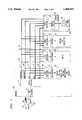
- FIG. 1is a block diagram of a telephone communication system including a terminal which is useful for describing the present invention
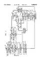
- FIG. 2shows the data format of various downlink and uplink messages
- FIG. 3shows a timing diagram illustrating how a slave processor seizes the OK lead during its associated byte interval
- FIG. 4shows a timing diagram illustrating how a slave processor may toggle its associated sanity lead
- FIG. 5is a flow chart describing the operation at a master processor
- FIGS. 6 and 7describe, respectively, the receive and transmit operations at a typical slave processor.
- each item or block of each figurehas a reference designation associated therewith, the first number of which refers to the figure in which that item is first located (e.g., 110 is located in FIG. 1 and step 602 is located in FIG. 6).
- FIG. 1Shown in FIG. 1 is an illustrative block diagram of a communication system useful for describing the operation of the present invention.
- the systemincludes common control unit 102 which connects to one or more central office (CO) or PBX lines 101 and which connects via extension lines 103, 104 to a plurality of station terminals 105-110.
- the communication systemmay be a Merlin® communication system such as described in U.S. Pat. No. 4,560,837 issued to Carson et al on Dec. 24, 1985. (Merlin is a registered trademark of AT&T).
- Each station terminal e.g., 110may, illustratively, be represented as including line interface 111, master processor 112 (including an internal program memory and data memory) and one or more secondary slave processors (120 and 130 in our example).
- the master processor 112connects to slave processors 120 and 130 over a communication bus 113.
- Communication bus 113includes a transmit path (TXD) 114, received path (RXD) 115, signaling path (OK) 116, and, optionally, address path 117 and sanity/reset path 118.
- An interface or connector 119enables one or more external adjuncts (also referred to hereinafter as devices) 140 and 150 to connect to communication bus 113.
- Slave processor 120connects via I/O interface 121 to user I/O unit 122 which includes elements such as terminal handset, dial pad, switch hook, buttons (line/feature) alerters, and light emitting diodes (LEDs).
- Slave processor 130connects via I/O interface 131 to display unit 132 of terminal 110. Obviously, the assignment of user input/output elements can be distributed differently between slave processors 120 and 130. Additionally, a different number of slave processors may be utilized.
- the external adjunctsmay include a well-known direct station selection (DSS) unit 140 and an adjunct interface 150 which interfaces personal computer (PC) 160 to communication bus 113.
- the DSS unit 140illustratively, includes slave processor 141, user interface 142 and a User I/O unit 143 including buttons, LEDs, and optionally a display unit.
- Adjunct interface 150illustratively, includes slave processor 151 and an RS-232 interface 152 which interfaces to PC 160.
- master processor 112uses the station communication protocol to communicate over communication bus 113 with both the internal slave processors 120 and 130 as well as the external slave processors 141 and 151 located, respectively, in DSS 140 and adjunct interface 150.
- Each downlink messageincludes one or more bytes each including a start bit, eight data bits, and a control bit.
- Downlink messagesare sent over bus TXD from the master to slave processors and can be of four types: data messages 201, 202; channel polls, 204; device polls, 203; and synchronization messages 205.
- Each downlink messagecontains two important features, the status byte 206 and the control or 9th bit. In the downlink message the status byte is used for flow control and device polling 203. The status byte is appended to all data messages 201, 202 and channel polls 204.
- a device poll message 203consists of only the status byte sent to the slave processors.
- the 9th data bit in each message byteis used as a control bit to signal the last byte in a message. All multi-byte messages have the 9th bit set to a logical "1" (e.g., 207), except for the last byte, which has the 9th bit (e.g., 208) set to a logical "0".
- a "0" control bittherefore, signals the last byte in a message sequence.
- the control bitis set to "0" in the status byte.
- Single byte device poll 203 or sync 205 messagesalways have the control bit set to "0".
- each slave processor 120, 130, 141 and 151When each slave processor 120, 130, 141 and 151 is first connected to bus 113 it must ignore the first downlink message, for it is not easily determined whether the bytes received are the entire message, or merely a portion. After discarding the first message, the downlink slave processors are now in sync, and are expected to process all further messages. This prevents slave processors that "come alive" in the middle of a transmission from attempting to decode an incomplete downlink message.
- Data message 201illustrates a generalized data message having N bytes, N-1 data bytes and one status byte, where N ⁇ M.
- Data message 202illustrates a data message having the minimum number of bytes, namely, M, one byte for each slave processor and one status byte. If master processor wants to transmit only one byte of data then the remaining M-1 data bytes of data message 202 have null data therein.
- the status bytecan be coded in two manners: response XON or response XOFF.
- response XONWhen master processor 112 determines that it can receive data back from slave processors, the status byte is coded response XON.
- a slave processor that currently has control of the uplink channelmay transmit an uplink message to the master processor 112.
- a response XOFFcontrarily, is sent when the master processor cannot accept new data.
- Channel polls 204are fixed length, multi-byte (M bytes) frames. Channel polls are sent periodically when the master processor does not have any data to send. Since the interface is half duplex and polled, this allows slave processors to send uplink data, without requiring the master processor first having to send data.
- a channel pollconsists of a number (M-1) of bytes set to null, with a control bit set to "1", followed by a status byte with a control bit set to "0".
- the master processor 112sends a device poll 203 to check for the existence of a specific slave processor.
- the device poll 203is a single byte message encoded with the address of the specific slave processor and with a control bit of "0".
- the masteruses this information to determine not only all the slave processors connected to bus 113, but, more importantly, which slave processors are connected to interface 119.
- the masterAfter sending the device poll, the master sends either a channel poll or data message, to give the slave processor in question an opportunity to send a data message 211 or device poll response 212.
- a slave processormay not respond directly to a device poll 203. It must wait until the next channel poll 204 or data message 201 to respond.
- the slave processor responses or "Uplink Messages"will be discussed in a later paragraph.
- Some slave processorsneed to maintain a synchronized time base, for example, to synchronize the LED flash patterns associated with line buttons on a DSS.
- the master processorsends a synchronization (sync) message at a time base that can subdivide each timing pattern an integral number of times.
- syncsynchronization
- a sync message 205is one byte encoded with the timing (e.g., flashing) pattern and with the control bit set to "0".
- a slave processormay not respond to a synchronization message. All slave processors have a table (not shown) that defines the states of their timing-dependent variables. After receiving the sync message 205 they reset their pointer in this table, and their time base, so that every slave processor is now at a predefined state. The offset into the table is chosen so that all the patterns are in the same state during the re-synchronization interval and the intervals before and after. This is to prevent "snapping" into a state, which could happen if the re-sync happened at a transition edge. Synchronization messages are also used for slave processor sanity verification. This will be discussed in a subsequent paragraph.
- Uplink messagesare sent over RXD path 114 from the slave processors to the master processor.
- Uplink messagesare similar to downlink messages.
- Data messages 211are used to send data from the slave processors to the master processor. They are multi-byte data frames having at least one data byte and one status byte and using the same format as master processor data message 201.
- Device poll responses 212are sent in response to a device poll from the master. Device poll responses are single byte frames including only a status byte.
- the control bitis used as previously described for downlink messages.
- the status byteis described as follows. In the uplink direction the status byte is used for adjunct identification (ID).
- IDadjunct identification
- the status/ID byte for each slave processoris unique and predefined, and appended to all data messages.
- Device poll responses 212consist only of an ID status byte. Device poll responses are sent after a slave device receives a device poll and must respond at the first opportunity it has to access the uplink channel. The device poll response is simply a status/ID byte sent by itself with the control bit set to "0".
- a device poll response 212is sent only when there is no data to send from a polled slave processor.
- a transmit priority schemeis needed.
- the slave processorsuse a signaling path 116 (OK lead) to signal that the uplink channel is in use.
- Each slave processoris assigned a byte of the downlink message after which it can check the OK lead and acquire control of the uplink channel (i.e., RXD path).
- Uplink data messages 211can only be sent after receipt of a multiple byte downlink message (data message 201 or channel poll 204).
- the slave processorscheck the first byte of the message and if the control bit is set to "0" then the message is single byte, and uplink messages cannot be sent.
- Each slave processorchecks the status of the OK lead 116 after receipt of a different preassigned byte.
- the first slave processor in the chaini.e., 120
- the second slave processor in the chaini.e., 130
- the third processor in the chain(i.e., 130) checks OK lead after it receives the third byte, and so on. Therefore as previously discussed, the minimum number of bytes in a downlink data message 201, 202 or channel poll 204 (including the status byte) must therefore be equal to the number of slave processors on the link (M in our example).
- All slave processorsmust seize the OK lead (i.e., set it to "0") prior to full receipt of the next byte (e.g., processor 1 must seize before end of byte 2), so that the OK lead is stable before the next slave processor in the chain checks.
- a slave processorOnce a slave processor has seized the OK lead, it must wait until the status byte (last byte of the message, with control bit set to "0") has been received, 301, before it can determine whether it may transmit an uplink message. If the status byte 206 is set to XON, the slave processor or device can begin transmitting the uplink data message 211 immediately after receiving the status byte. If the status byte 206 is set to XOFF, then no uplink message may be sent. The slave processor should not relinquish control of the OK lead, however, in order to keep data messages from the various slave processors in time-order. The waiting slave processor holds the OK lead seized and continues to check subsequent status bytes until an XON status byte is sent again, after which it sends its data message.
- Data transmission from other slave processorswill then wait until the waiting slave processor transmits, thereby preserving the order of data transmission.
- This data transmission orderensures that the timing of events at different slave processors are received in the correct order at master processor unit 112.
- Channel pollsare sent with XOFF status byte in order to allow slave processor to gain control of OK lead, but then not actually transmit data until the master processor is ready.
- control of the OK leadsignifies continuing events.
- a slave processorcan hold the OK lead and block the uplink channel.
- OK leadis released or dropped, and other slave processors can now transmit. While being blocked, a slave processor waiting to transmit needs to determine whether to buffer or discard its data. This depends on the type of data and is determined by the type of data being handled by a slave processor.
- Slave processors on the bus 113may optionally include a sanity verification.
- individual sanity and reset leadsare connected from each slave processor (120, 130, 141 and 151) to the master processor 112, via bus 118.
- a slave processorreceives a sync message 205 it must toggle the state of its sanity lead. If it does not, the master processor 112 assumes a sanity error has occurred and sends a reset signal over the reset lead to the slave processor. This is shown in FIG.
- slave processors 120 and 130have toggled their sanity leads, respectively, sanity leads 1 and 2, while slave processor 141 and 151 have not toggled their sanity leads, respectively, sanity leads 3 and 4.
- master processor 112resets slave processors 141 and 151 via their associated reset leads. If a slave processor maintains its own sanity then this interface is not necessary.
- Some slave processors on bus 113may have their sanity controlled by the master processor 112, and others may control it themselves.
- the addressing bus 117can be used to send information to specify the priority number of the slave processors. Addressing can take two forms: either all slave processors "know" where they are in the chain (i.e., on bus 113), and are hard coded with this information; or they support an addressing interface. Different slave processors on the same link can use different methods.
- the addressing bus 117consists of n-leads, where n is equal to log base 2 of the number of secondary devices connected to the addressing bus 117. In our example, two leads are needed to uniquely address four slave processors.
- step 501the transmit process begins.
- step 503the intermessage timer is checked.
- the intermessage timeris set to different timer values depending on the downlink message transmitted. This timer allows the slave processors enough time to respond to any message sent by the master processor 112. If the intermessage timer has expired, then step 505 is performed, otherwise the master processor 112 waits until that timer has expired.
- step 505it is determined if data originating from control unit 102 or master processor 112 is available to send to slave processors 120, 130, 141 or 151. If data is available then in step 507 the master processor builds the data message 201.
- step 517master processor transmits the multi-byte data message over lead TXD lead 115. In step 519 control is returned to step 501.
- step 505if no data is available from either control unit 102 or master processor 112 then, in step 521 it is determined if the channel poll timer has expired. If it has, then in step 523 master processor builds a null channel poll message as shown in 204. In step 525 the intermessage timer is set to a value B (where B is less than C). Following step 525 steps 515, 517 and 519 are performed as previously described. Returning to step 521, if the channel poll timer has not expired then in step 527 it is determined if the slave poll timer has expired. The slave poll timer is used to determine, worst case, how often master processor 112 checks (using a device poll message 203) if the various slave processors (devices) are still active or present.
- step 529it is determined if the last polled slave processor has responded. This is determined by checking a slave status buffer at the master processor associated with that slave processor or device. If the answer to step 529 is no, then in step 531 it is determined if the OK lead was idle at any time since the last poll was sent. If the OK lead was not idle then master processor builds a device poll message to be sent to the same device. Note, an idle OK lead means that no slave processor is ready to transmit.
- step 535the intermessage timer is set to a value A (where A is less than B).
- step 537the slave poll timer is reset.
- master processortransmits the single byte message over TXD lead 115. Thereafter, control returns to the start step 501.
- step 541master processor marks that device or slave processor as not being present. Thus, the uplink channel was available and the polled device did not respond.
- step 543master processor builds a device poll message (e.g., 203) for the next device or slave processor. Following step 543 step 535 is performed as previously described.
- step 545master processor marks the slave status buffer for that slave processor or device as being present on bus 113. Thereafter, step 543 is performed as previously described.
- step 547the master processor determines if the LED sync timer has expired. If it has, then in step 549 the master processor 112 builds an LED sync message. Thereafter step 535 is performed as previously described. In step 547 if the LED sync timer has not expired, then control returns to the start step 501. The sync timer ensures that the slave processors will periodically be synchronized.
- the sync timer and slave poll timermay be approximately two seconds, the channel poll timer may be 30 to 50 milliseconds, while the various inter-message timer values (A, B, C) may vary from 2 to 15 milliseconds.
- step 600the slave processor determines if a received byte is the last byte of a downlink message. Recall that a last byte can be determined by checking for a control bit equal to zero. If it is not the last byte, then in step 603 it is determined if it is the first byte of a message. If it is, then step 607 is performed. In step 607 it is determined if this slave processor is the first slave processor. This is done by checking a slave address buffer.
- step 609it is determined if the byte number is one assigned to the slave processor. That is, is the byte number one plus the slave processor number. If it is, then in step 611 the slave processor monitors the OK lead and determines if the OK lead is already in the held or seized state. If it is, in step 613 it is determined if this particular slave processor is holding the OK lead. If the answer is yes, then in step 615 the slave processor determines if it has any data to send to master processor over RXD lead 114. If there is no data to send, then in step 617 it is determined if the received message is the first message received. In step 615 if there was data to send, then in step 619 the slave processor starts to transmit.
- step 617is performed as previously described.
- controlreturns in step 621.
- step 617if the first message was not received, then in step 623 the slave processor stores the received byte and updates the buffer pointer.
- step 621is performed as previously described.
- step 625the slave processor's messages are dropped. This is optionally done to prevent out-of-sequence events from different slave processors. Thereafter step 617 is performed as previously described.
- step 611if the OK lead is not held, then in step 627 it is determined if the slave processor has any data to send. If it does not then control is transferred to step 617. If there is data to send, then in step 629 the slave processor establishes a seized state on the OK lead. Thereafter, the slave processor starts to transmit. Thereafter step 617 is performed as previously described.
- step 609if it is determined that the slave processor is not associated with the received byte, then control is transferred to the previously-described step 617.
- step 603if it is determined that the received byte is not the first byte then control is transferred to step 616.
- step 616it is determined if the byte number is equal to one plus the slave processor number. If it is, then control transfers to the previously-described step 609. Otherwise, control transfers to the previously-described step 617.
- step 631the slave processor determines whether the poll or sync message, respectively, 202 and 205, have been received. Thus, in step 631 it is determined whether the last byte is, in fact, the first byte. If in step 631 a poll or sync message was received, then in step 633 it is determined whether the message was a poll message. If it was, then in step 635 it is determined if the poll message was directed to this slave processor. If the answer is yes, then slave processor sets its "poll response due" flag in step 637 and control returns to the previously-described step 621. In step 635 if the poll message was not for this slave processor then control transfers to step 621.
- step 633if no poll message was received, then in step 639 it is determined that a sync message was received, synchronization is reset and the optional sanity lead 118 is toggled. Thereafter, control transfers to the previously-described step 621.
- step 631if the receive byte was not the poll or sync message, then in step 641 it is determined whether the message should be ignored. If the message should not be ignored, then the "message received" flag is set in step 643. In step 645 it is determined if the XON state exists in the status byte of data message 201. In step 641, if it's determined that the message should be ignored then control is also transferred to step 645. In step 645, if the XON status does not exist, then the previously-described 621 is performed. In step 645, if the XON status exists, then in step 647, slave processor determines if it has data to transmit. If no data exists, then control returns to step 621. If data exists, then in step 649 the "start transmit" flag is set and control transfers to step 621.
- step 703it is determined if transmission has started. If not then the slave processor periodically checks if transmission has started. When transmission has finally started, then in step 705 it is determined if the slave processor's message transmission is done. If it is not done, then in step 706 it is determined if there is more data which is buffered and ready for transmission. If there is no more data, then in step 707 the "transmit done" flag is set, a status byte is generated, the control bit of that status byte is set to logic zero, and that status byte transmitted. Following step 707, the slave processor rearms the receive interrupt and control is returned in step 703.
- step 711the slave processor obtains the next data byte and sends that data byte in an uplink message. Thereafter, control transfers to the previously-described step 703.
- step 705if it is determined that the transmit operation is complete, then in step 713 the slave processor determines if it should clear the OK lead. If the OK lead should not be cleared then in step 715 the "transmit done" flag is cleared, i.e., transmission is finished, and control returns to step 703. In step 713, if it is determined that the OK lead should be cleared, then in step 717 the slave processor drops the OK lead.
Landscapes
- Engineering & Computer Science (AREA)
- Computer Networks & Wireless Communication (AREA)
- Signal Processing (AREA)
- Computer Security & Cryptography (AREA)
- Computer Hardware Design (AREA)
- General Engineering & Computer Science (AREA)
- Communication Control (AREA)
Abstract
Description
Claims (20)
Priority Applications (1)
| Application Number | Priority Date | Filing Date | Title |
|---|---|---|---|
| US07/903,304US5488693A (en) | 1992-06-24 | 1992-06-24 | Protocol with control bits and bytes for controlling the order of communications between a master processor and plural slave processors |
Applications Claiming Priority (1)
| Application Number | Priority Date | Filing Date | Title |
|---|---|---|---|
| US07/903,304US5488693A (en) | 1992-06-24 | 1992-06-24 | Protocol with control bits and bytes for controlling the order of communications between a master processor and plural slave processors |
Publications (1)
| Publication Number | Publication Date |
|---|---|
| US5488693Atrue US5488693A (en) | 1996-01-30 |
Family
ID=25417274
Family Applications (1)
| Application Number | Title | Priority Date | Filing Date |
|---|---|---|---|
| US07/903,304Expired - LifetimeUS5488693A (en) | 1992-06-24 | 1992-06-24 | Protocol with control bits and bytes for controlling the order of communications between a master processor and plural slave processors |
Country Status (1)
| Country | Link |
|---|---|
| US (1) | US5488693A (en) |
Cited By (21)
| Publication number | Priority date | Publication date | Assignee | Title |
|---|---|---|---|---|
| US5809222A (en)* | 1995-09-11 | 1998-09-15 | Kabushiki Kaisha Toshiba | Method and apparatus for controlling continuous data server using more than one central control devices |
| US5960209A (en)* | 1996-03-11 | 1999-09-28 | Mitel Corporation | Scaleable digital signal processor with parallel architecture |
| GB2341765A (en)* | 1998-09-18 | 2000-03-22 | Pixelfusion Ltd | Bus idle usage |
| US6430218B1 (en)* | 1997-06-25 | 2002-08-06 | Mitsubishi Denki Kabushiki Kaisha | Communication control apparatus |
| WO2003055152A1 (en)* | 2001-11-06 | 2003-07-03 | Universitat Rovira I Virgili | Serial communication protocol with a master-slave operating scheme |
| US6597921B2 (en)* | 2000-12-22 | 2003-07-22 | Sbc Properties, Lp | Method and system for protocol feature communication |
| US6721321B1 (en)* | 1998-12-30 | 2004-04-13 | Samsung Electronics Co., Ltd. | Data communication channel processing apparatus for transmitter, protocol stack structure and operating method therefor |
| US20040073649A1 (en)* | 2002-08-30 | 2004-04-15 | Satoshi Inami | Stream data processing apparatus |
| US20050114463A1 (en)* | 2003-11-20 | 2005-05-26 | Hyundai Mobis Co., Ltd. | Multi-microprocessor apparatus and slave reset method for the same |
| US20060259155A1 (en)* | 2005-05-12 | 2006-11-16 | Mitsubishi Denki Kabushiki Kaisha | Control and monitoring system for power system |
| US20070161391A1 (en)* | 2003-06-02 | 2007-07-12 | Thandu Balasubramaniam Kulasek | Method and system for protocol feature communication |
| US20080037444A1 (en)* | 2006-08-08 | 2008-02-14 | Marvell Semiconductor, Inc. | Ad-hoc simple configuration |
| US20080172491A1 (en)* | 2006-10-16 | 2008-07-17 | Marvell Semiconductor Inc | Automatic ad-hoc network creation and coalescing using wps |
| US20090011834A1 (en)* | 2007-07-03 | 2009-01-08 | Kapil Chhabra | Location aware ad-hoc gaming |
| US20090192718A1 (en)* | 2008-01-30 | 2009-07-30 | Chevron U.S.A. Inc. | Subsurface prediction method and system |
| US7633963B1 (en)* | 1999-09-22 | 2009-12-15 | Plantronics, Inc. | Accessory interface bus for telephone headset adapter |
| US20100153602A1 (en)* | 2008-12-12 | 2010-06-17 | Fujitsu Microelectronics Limited | Computer system and abnormality detection circuit |
| US7925753B2 (en) | 2002-08-30 | 2011-04-12 | Panasonic Corporation | Stream data processing apparatus |
| US8233456B1 (en) | 2006-10-16 | 2012-07-31 | Marvell International Ltd. | Power save mechanisms for dynamic ad-hoc networks |
| US9308455B1 (en) | 2006-10-25 | 2016-04-12 | Marvell International Ltd. | System and method for gaming in an ad-hoc network |
| US20210297283A1 (en)* | 2020-03-17 | 2021-09-23 | Canon Kabushiki Kaisha | Master slave communication system capable of reducing manufacturing cost, electronic device, control method for master slave communication system, and control method for electronic device |
Citations (9)
| Publication number | Priority date | Publication date | Assignee | Title |
|---|---|---|---|---|
| US3728681A (en)* | 1972-01-06 | 1973-04-17 | Collins Radio Co | Data loop communication priority establishing apparatus |
| US4145739A (en)* | 1977-06-20 | 1979-03-20 | Wang Laboratories, Inc. | Distributed data processing system |
| US4148011A (en)* | 1977-06-06 | 1979-04-03 | General Automation, Inc. | Asynchronous priority circuit for controlling access to a bus |
| US4281380A (en)* | 1978-12-27 | 1981-07-28 | Harris Corporation | Bus collision avoidance system for distributed network data processing communications system |
| US4598363A (en)* | 1983-07-07 | 1986-07-01 | At&T Bell Laboratories | Adaptive delayed polling of sensors |
| US4888728A (en)* | 1986-03-29 | 1989-12-19 | Kabushiki Kaisha Toshiba | Multipoint link data-transmission control system |
| US4920486A (en)* | 1987-11-23 | 1990-04-24 | Digital Equipment Corporation | Distributed arbitration apparatus and method for shared bus |
| US5049872A (en)* | 1987-09-14 | 1991-09-17 | Mitsubishi Denki Kabushiki Kaisha | Remote supervisory control system |
| US5059926A (en)* | 1991-03-13 | 1991-10-22 | Motorola, Inc. | Frequency synchronization apparatus |
- 1992
- 1992-06-24USUS07/903,304patent/US5488693A/ennot_activeExpired - Lifetime
Patent Citations (9)
| Publication number | Priority date | Publication date | Assignee | Title |
|---|---|---|---|---|
| US3728681A (en)* | 1972-01-06 | 1973-04-17 | Collins Radio Co | Data loop communication priority establishing apparatus |
| US4148011A (en)* | 1977-06-06 | 1979-04-03 | General Automation, Inc. | Asynchronous priority circuit for controlling access to a bus |
| US4145739A (en)* | 1977-06-20 | 1979-03-20 | Wang Laboratories, Inc. | Distributed data processing system |
| US4281380A (en)* | 1978-12-27 | 1981-07-28 | Harris Corporation | Bus collision avoidance system for distributed network data processing communications system |
| US4598363A (en)* | 1983-07-07 | 1986-07-01 | At&T Bell Laboratories | Adaptive delayed polling of sensors |
| US4888728A (en)* | 1986-03-29 | 1989-12-19 | Kabushiki Kaisha Toshiba | Multipoint link data-transmission control system |
| US5049872A (en)* | 1987-09-14 | 1991-09-17 | Mitsubishi Denki Kabushiki Kaisha | Remote supervisory control system |
| US4920486A (en)* | 1987-11-23 | 1990-04-24 | Digital Equipment Corporation | Distributed arbitration apparatus and method for shared bus |
| US5059926A (en)* | 1991-03-13 | 1991-10-22 | Motorola, Inc. | Frequency synchronization apparatus |
Cited By (35)
| Publication number | Priority date | Publication date | Assignee | Title |
|---|---|---|---|---|
| US5809222A (en)* | 1995-09-11 | 1998-09-15 | Kabushiki Kaisha Toshiba | Method and apparatus for controlling continuous data server using more than one central control devices |
| US5960209A (en)* | 1996-03-11 | 1999-09-28 | Mitel Corporation | Scaleable digital signal processor with parallel architecture |
| US6430218B1 (en)* | 1997-06-25 | 2002-08-06 | Mitsubishi Denki Kabushiki Kaisha | Communication control apparatus |
| GB2341765B (en)* | 1998-09-18 | 2003-10-22 | Pixelfusion Ltd | Idle bus usage |
| GB2341765A (en)* | 1998-09-18 | 2000-03-22 | Pixelfusion Ltd | Bus idle usage |
| US6721321B1 (en)* | 1998-12-30 | 2004-04-13 | Samsung Electronics Co., Ltd. | Data communication channel processing apparatus for transmitter, protocol stack structure and operating method therefor |
| US7633963B1 (en)* | 1999-09-22 | 2009-12-15 | Plantronics, Inc. | Accessory interface bus for telephone headset adapter |
| US6597921B2 (en)* | 2000-12-22 | 2003-07-22 | Sbc Properties, Lp | Method and system for protocol feature communication |
| US20040014458A1 (en)* | 2000-12-22 | 2004-01-22 | Thandu Balasubramaniam Kulasekaran | Method and system for protocol feature communication |
| US7209761B2 (en) | 2000-12-22 | 2007-04-24 | Sbc Technology Resources, Inc. | Method and system for protocol feature communication |
| WO2003055152A1 (en)* | 2001-11-06 | 2003-07-03 | Universitat Rovira I Virgili | Serial communication protocol with a master-slave operating scheme |
| US20040073649A1 (en)* | 2002-08-30 | 2004-04-15 | Satoshi Inami | Stream data processing apparatus |
| US7925753B2 (en) | 2002-08-30 | 2011-04-12 | Panasonic Corporation | Stream data processing apparatus |
| US20070161391A1 (en)* | 2003-06-02 | 2007-07-12 | Thandu Balasubramaniam Kulasek | Method and system for protocol feature communication |
| US7580720B2 (en) | 2003-06-02 | 2009-08-25 | At&T Intellectual Property I, L.P. | Method and system for protocol feature communication |
| US20050114463A1 (en)* | 2003-11-20 | 2005-05-26 | Hyundai Mobis Co., Ltd. | Multi-microprocessor apparatus and slave reset method for the same |
| US7389327B2 (en)* | 2005-05-12 | 2008-06-17 | Mitsubishi Denki Kabushiki Kaisha | Control and monitoring system for power system |
| US20060259155A1 (en)* | 2005-05-12 | 2006-11-16 | Mitsubishi Denki Kabushiki Kaisha | Control and monitoring system for power system |
| US9019866B2 (en) | 2006-08-08 | 2015-04-28 | Marvell World Trade Ltd. | Ad-hoc simple configuration |
| US8619623B2 (en)* | 2006-08-08 | 2013-12-31 | Marvell World Trade Ltd. | Ad-hoc simple configuration |
| US20080037444A1 (en)* | 2006-08-08 | 2008-02-14 | Marvell Semiconductor, Inc. | Ad-hoc simple configuration |
| US20080172491A1 (en)* | 2006-10-16 | 2008-07-17 | Marvell Semiconductor Inc | Automatic ad-hoc network creation and coalescing using wps |
| US9374785B1 (en) | 2006-10-16 | 2016-06-21 | Marvell International Ltd. | Power save mechanisms for dynamic ad-hoc networks |
| US9444874B2 (en) | 2006-10-16 | 2016-09-13 | Marvell International Ltd. | Automatic Ad-Hoc network creation and coalescing using WPS |
| US8233456B1 (en) | 2006-10-16 | 2012-07-31 | Marvell International Ltd. | Power save mechanisms for dynamic ad-hoc networks |
| US8732315B2 (en) | 2006-10-16 | 2014-05-20 | Marvell International Ltd. | Automatic ad-hoc network creation and coalescing using WiFi protected setup |
| US9308455B1 (en) | 2006-10-25 | 2016-04-12 | Marvell International Ltd. | System and method for gaming in an ad-hoc network |
| US8628420B2 (en) | 2007-07-03 | 2014-01-14 | Marvell World Trade Ltd. | Location aware ad-hoc gaming |
| US20090011834A1 (en)* | 2007-07-03 | 2009-01-08 | Kapil Chhabra | Location aware ad-hoc gaming |
| US20090192718A1 (en)* | 2008-01-30 | 2009-07-30 | Chevron U.S.A. Inc. | Subsurface prediction method and system |
| US7869955B2 (en) | 2008-01-30 | 2011-01-11 | Chevron U.S.A. Inc. | Subsurface prediction method and system |
| US8700835B2 (en)* | 2008-12-12 | 2014-04-15 | Fujitsu Semiconductor Limited | Computer system and abnormality detection circuit |
| US20100153602A1 (en)* | 2008-12-12 | 2010-06-17 | Fujitsu Microelectronics Limited | Computer system and abnormality detection circuit |
| US20210297283A1 (en)* | 2020-03-17 | 2021-09-23 | Canon Kabushiki Kaisha | Master slave communication system capable of reducing manufacturing cost, electronic device, control method for master slave communication system, and control method for electronic device |
| US11700144B2 (en)* | 2020-03-17 | 2023-07-11 | Canon Kabushiki Kaisha | Master slave communication system and control method for master slave communication system |
Similar Documents
| Publication | Publication Date | Title |
|---|---|---|
| US5488693A (en) | Protocol with control bits and bytes for controlling the order of communications between a master processor and plural slave processors | |
| EP0100662B1 (en) | Digital communication system | |
| EP0153328B1 (en) | Data conference arrangement | |
| JP2840070B2 (en) | Time division multiplex switching system for pulse code modulated telephone signals. | |
| EP0060517A1 (en) | Multiple access system of terminals on a digital telephone line | |
| US4512017A (en) | Digital dual channel communication terminal | |
| US4512016A (en) | Digital communication station signaling control | |
| US6452946B1 (en) | Apparatus and method for improving performance in master and slave communications systems | |
| US5201045A (en) | Arrangement and method of downloading data to a plurality of destinations in a digital telephone system | |
| US4853956A (en) | Communication system distributed processing message delivery system | |
| KR960007585B1 (en) | Switch-path reservation arrangement | |
| US4858230A (en) | Multiport/multidrop computer communications | |
| US6751232B1 (en) | Method and apparatus for communicating data between first and second pairs of transceivers communicating on a common communications link | |
| JPH0473178B2 (en) | ||
| JP2814497B2 (en) | Signal link control device | |
| JPH0358214B2 (en) | ||
| JP2506164B2 (en) | Measuring method of network characteristics | |
| JPS6128252A (en) | Transmitter possible for extension transfer | |
| JPS6224746A (en) | Terminal control system | |
| JPH0687560B2 (en) | Information simultaneous notification method | |
| JPS5989065A (en) | Facsimile communication system | |
| JPH0324839A (en) | terminal adapter | |
| JPS6096092A (en) | Button telephone device | |
| JPS58173941A (en) | Health check system of communication device | |
| JPH0834526B2 (en) | Communication terminal |
Legal Events
| Date | Code | Title | Description |
|---|---|---|---|
| AS | Assignment | Owner name:AMERICAN TELEPHONE AND TELEGRAPH COMPANY, A CORP. Free format text:ASSIGNMENT OF ASSIGNORS INTEREST.;ASSIGNORS:HOUCK, WARREN B.;ILLUZZI, VINCENT A.;RICKER, MARY E.;AND OTHERS;REEL/FRAME:006173/0680;SIGNING DATES FROM 19920617 TO 19920619 | |
| AS | Assignment | Owner name:AT&T IPM CORP., FLORIDA Free format text:ASSIGNMENT OF ASSIGNORS INTEREST;ASSIGNOR:AT&T CORP.;REEL/FRAME:007528/0038 Effective date:19950523 Owner name:AT&T CORP., NEW YORK Free format text:ASSIGNMENT OF ASSIGNORS INTEREST;ASSIGNOR:AMERICAN TELELPHONE AND TELEGRAPH COMPANY;REEL/FRAME:007527/0274 Effective date:19940420 | |
| STCF | Information on status: patent grant | Free format text:PATENTED CASE | |
| FEPP | Fee payment procedure | Free format text:PAYOR NUMBER ASSIGNED (ORIGINAL EVENT CODE: ASPN); ENTITY STATUS OF PATENT OWNER: LARGE ENTITY | |
| FPAY | Fee payment | Year of fee payment:4 | |
| AS | Assignment | Owner name:LUCENT TECHNOLOGIES, INC., NEW JERSEY Free format text:ASSIGNMENT OF ASSIGNORS INTEREST;ASSIGNOR:AT&T CORP.;REEL/FRAME:012754/0365 Effective date:19960329 Owner name:AVAYA TECHNOLOGY CORP., NEW JERSEY Free format text:ASSIGNMENT OF ASSIGNORS INTEREST;ASSIGNOR:LUCENT TECHNOLOGIES INC.;REEL/FRAME:012754/0770 Effective date:20000929 | |
| AS | Assignment | Owner name:BANK OF NEW YORK, THE, NEW YORK Free format text:SECURITY AGREEMENT;ASSIGNOR:AVAYA TECHNOLOGY CORP.;REEL/FRAME:012775/0149 Effective date:20020405 | |
| FPAY | Fee payment | Year of fee payment:8 | |
| FPAY | Fee payment | Year of fee payment:12 | |
| AS | Assignment | Owner name:CITIBANK, N.A., AS ADMINISTRATIVE AGENT, NEW YORK Free format text:SECURITY AGREEMENT;ASSIGNORS:AVAYA, INC.;AVAYA TECHNOLOGY LLC;OCTEL COMMUNICATIONS LLC;AND OTHERS;REEL/FRAME:020156/0149 Effective date:20071026 Owner name:CITIBANK, N.A., AS ADMINISTRATIVE AGENT,NEW YORK Free format text:SECURITY AGREEMENT;ASSIGNORS:AVAYA, INC.;AVAYA TECHNOLOGY LLC;OCTEL COMMUNICATIONS LLC;AND OTHERS;REEL/FRAME:020156/0149 Effective date:20071026 | |
| AS | Assignment | Owner name:CITICORP USA, INC., AS ADMINISTRATIVE AGENT, NEW Y Free format text:SECURITY AGREEMENT;ASSIGNORS:AVAYA, INC.;AVAYA TECHNOLOGY LLC;OCTEL COMMUNICATIONS LLC;AND OTHERS;REEL/FRAME:020166/0705 Effective date:20071026 Owner name:CITICORP USA, INC., AS ADMINISTRATIVE AGENT, NEW YORK Free format text:SECURITY AGREEMENT;ASSIGNORS:AVAYA, INC.;AVAYA TECHNOLOGY LLC;OCTEL COMMUNICATIONS LLC;AND OTHERS;REEL/FRAME:020166/0705 Effective date:20071026 Owner name:CITICORP USA, INC., AS ADMINISTRATIVE AGENT,NEW YO Free format text:SECURITY AGREEMENT;ASSIGNORS:AVAYA, INC.;AVAYA TECHNOLOGY LLC;OCTEL COMMUNICATIONS LLC;AND OTHERS;REEL/FRAME:020166/0705 Effective date:20071026 | |
| AS | Assignment | Owner name:AVAYA INC., NEW JERSEY Free format text:REASSIGNMENT;ASSIGNOR:AVAYA TECHNOLOGY LLC;REEL/FRAME:021158/0290 Effective date:20080625 | |
| FEPP | Fee payment procedure | Free format text:PAYOR NUMBER ASSIGNED (ORIGINAL EVENT CODE: ASPN); ENTITY STATUS OF PATENT OWNER: LARGE ENTITY Free format text:PAYER NUMBER DE-ASSIGNED (ORIGINAL EVENT CODE: RMPN); ENTITY STATUS OF PATENT OWNER: LARGE ENTITY | |
| AS | Assignment | Owner name:AVAYA TECHNOLOGY LLC, NEW JERSEY Free format text:CONVERSION FROM CORP TO LLC;ASSIGNOR:AVAYA TECHNOLOGY CORP.;REEL/FRAME:022071/0420 Effective date:20051004 | |
| AS | Assignment | Owner name:BANK OF NEW YORK MELLON TRUST, NA, AS NOTES COLLATERAL AGENT, THE, PENNSYLVANIA Free format text:SECURITY AGREEMENT;ASSIGNOR:AVAYA INC., A DELAWARE CORPORATION;REEL/FRAME:025863/0535 Effective date:20110211 Owner name:BANK OF NEW YORK MELLON TRUST, NA, AS NOTES COLLAT Free format text:SECURITY AGREEMENT;ASSIGNOR:AVAYA INC., A DELAWARE CORPORATION;REEL/FRAME:025863/0535 Effective date:20110211 | |
| AS | Assignment | Owner name:AVAYA INC., CALIFORNIA Free format text:BANKRUPTCY COURT ORDER RELEASING ALL LIENS INCLUDING THE SECURITY INTEREST RECORDED AT REEL/FRAME 025863/0535;ASSIGNOR:THE BANK OF NEW YORK MELLON TRUST, NA;REEL/FRAME:044892/0001 Effective date:20171128 Owner name:AVAYA INC. (FORMERLY KNOWN AS AVAYA TECHNOLOGY COR Free format text:BANKRUPTCY COURT ORDER RELEASING ALL LIENS INCLUDING THE SECURITY INTEREST RECORDED AT REEL/FRAME 012775/0149;ASSIGNOR:THE BANK OF NEW YORK;REEL/FRAME:044893/0266 Effective date:20171128 | |
| AS | Assignment | Owner name:AVAYA TECHNOLOGY, LLC, NEW JERSEY Free format text:RELEASE BY SECURED PARTY;ASSIGNOR:CITICORP USA, INC.;REEL/FRAME:045032/0213 Effective date:20171215 Owner name:AVAYA, INC., CALIFORNIA Free format text:RELEASE BY SECURED PARTY;ASSIGNOR:CITICORP USA, INC.;REEL/FRAME:045032/0213 Effective date:20171215 Owner name:VPNET TECHNOLOGIES, INC., NEW JERSEY Free format text:RELEASE BY SECURED PARTY;ASSIGNOR:CITICORP USA, INC.;REEL/FRAME:045032/0213 Effective date:20171215 Owner name:OCTEL COMMUNICATIONS LLC, CALIFORNIA Free format text:RELEASE BY SECURED PARTY;ASSIGNOR:CITICORP USA, INC.;REEL/FRAME:045032/0213 Effective date:20171215 Owner name:SIERRA HOLDINGS CORP., NEW JERSEY Free format text:RELEASE BY SECURED PARTY;ASSIGNOR:CITICORP USA, INC.;REEL/FRAME:045032/0213 Effective date:20171215 |