US5487184A - Offset transmission line coupler for radio frequency signal amplifiers - Google Patents
Offset transmission line coupler for radio frequency signal amplifiersDownload PDFInfo
- Publication number
- US5487184A US5487184AUS08/150,504US15050493AUS5487184AUS 5487184 AUS5487184 AUS 5487184AUS 15050493 AUS15050493 AUS 15050493AUS 5487184 AUS5487184 AUS 5487184A
- Authority
- US
- United States
- Prior art keywords
- transmission line
- signal
- substrate
- portions
- coupled
- Prior art date
- Legal status (The legal status is an assumption and is not a legal conclusion. Google has not performed a legal analysis and makes no representation as to the accuracy of the status listed.)
- Expired - Lifetime
Links
- 230000005540biological transmissionEffects0.000titleclaimsabstractdescription208
- 230000008878couplingEffects0.000claimsabstractdescription47
- 238000010168coupling processMethods0.000claimsabstractdescription47
- 238000005859coupling reactionMethods0.000claimsabstractdescription47
- 239000000758substrateSubstances0.000claimsdescription42
- 230000001413cellular effectEffects0.000claimsdescription16
- 239000011248coating agentSubstances0.000claims5
- 238000000576coating methodMethods0.000claims5
- 239000002131composite materialSubstances0.000claims1
- 238000007747platingMethods0.000abstractdescription13
- 230000035945sensitivityEffects0.000abstractdescription4
- 230000002708enhancing effectEffects0.000abstractdescription3
- 230000015556catabolic processEffects0.000abstractdescription2
- 238000006731degradation reactionMethods0.000abstractdescription2
- 239000003990capacitorSubstances0.000description12
- 238000010586diagramMethods0.000description5
- 238000003780insertionMethods0.000description4
- 230000037431insertionEffects0.000description4
- 239000000463materialSubstances0.000description3
- 238000000034methodMethods0.000description3
- 239000004020conductorSubstances0.000description2
- PNEYBMLMFCGWSK-UHFFFAOYSA-Naluminium oxideInorganic materials[O-2].[O-2].[O-2].[Al+3].[Al+3]PNEYBMLMFCGWSK-UHFFFAOYSA-N0.000description1
- 230000003321amplificationEffects0.000description1
- 230000003247decreasing effectEffects0.000description1
- 230000000593degrading effectEffects0.000description1
- 230000001419dependent effectEffects0.000description1
- 238000001514detection methodMethods0.000description1
- -1duroidInorganic materials0.000description1
- 239000011152fibreglassSubstances0.000description1
- 230000005669field effectEffects0.000description1
- 238000003475laminationMethods0.000description1
- 238000003199nucleic acid amplification methodMethods0.000description1
- 239000010453quartzSubstances0.000description1
- VYPSYNLAJGMNEJ-UHFFFAOYSA-Nsilicon dioxideInorganic materialsO=[Si]=OVYPSYNLAJGMNEJ-UHFFFAOYSA-N0.000description1
Images


Classifications
- H—ELECTRICITY
- H01—ELECTRIC ELEMENTS
- H01P—WAVEGUIDES; RESONATORS, LINES, OR OTHER DEVICES OF THE WAVEGUIDE TYPE
- H01P5/00—Coupling devices of the waveguide type
- H01P5/12—Coupling devices having more than two ports
- H01P5/16—Conjugate devices, i.e. devices having at least one port decoupled from one other port
- H01P5/18—Conjugate devices, i.e. devices having at least one port decoupled from one other port consisting of two coupled guides, e.g. directional couplers
- H01P5/184—Conjugate devices, i.e. devices having at least one port decoupled from one other port consisting of two coupled guides, e.g. directional couplers the guides being strip lines or microstrips
- H01P5/187—Broadside coupled lines
- H—ELECTRICITY
- H04—ELECTRIC COMMUNICATION TECHNIQUE
- H04W—WIRELESS COMMUNICATION NETWORKS
- H04W52/00—Power management, e.g. Transmission Power Control [TPC] or power classes
- H04W52/04—Transmission power control [TPC]
Definitions
- the present inventionis generally related to radio frequency (RF) signal couplers, and more particularly to an offset transmission line coupler for RF signal amplifiers of cellular telephones.
- RFradio frequency
- RF signal couplershave been implemented by several methods, including by means of capacitive couplers or transmission line couplers.
- Prior transmission line couplerstypically have been implemented by a first transmission line on the top surface of a top layer of a multi-layer circuit board and a second transmission line on the bottom surface of the top layer, directly under and electromagnetically coupled to the first transmission line.
- a ground planeis disposed on the bottom surface of a bottom layer of the circuit board, which is laminated to the top layer.
- the top layer of the circuit boardis of sufficient thickness to achieve a desired amount of coupling between the first and second transmission lines.
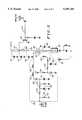
- FIG. 1is a block diagram of RF transmitter circuitry 100, which may advantageously utilize the present invention.
- FIG. 2is a block diagram of a cellular telephone 200 including RF transmitter circuitry 100.
- FIG. 3is a detailed circuit diagram of amplifier 103 and power detect circuitry 109 in FIG. 1.
- FIG. 4is a section of a circuit board of the transmitter circuitry in FIG. 1, showing transmission line coupler 115.
- FIG. 5is a top view of the top layer 321 of the circuit board section in FIG. 4, showing an embodiment of transmission lines 201 and 202 of transmission line coupler 115.
- FIG. 6is a top view of the top layer 321 of the circuit board section in FIG. 4, showing the preferred embodiment of transmission lines 201 and 202 of transmission line coupler 115.
- FIG. 7is a top view of the top layer 321 of the circuit board section in FIG. 4, showing an alternate embodiment of transmission lines 201 and 202 of transmission line coupler 115.
- the present inventionencompasses RF signal coupler circuitry for detecting an RF signal generated by a signal source and producing an RF detect signal.
- the RF signal coupler circuitrycomprises a substrate having top and bottom surfaces and a predetermined dielectric constant; a first transmission line having a predetermined shape and being disposed on the top surface of the substrate, the first transmission line coupled to the RF signal; and a second transmission line disposed on the bottom surface of the substrate, the second transmission line having at least first and second portions electromagnetically coupled to the first transmission line for generating the RF detect signal having an amplitude related to the amplitude of the RF signal, the first portion being offset a first predetermined distance to one side of the first transmission line, the second portion being offset a second predetermined distance to the other side of the first transmission line, the amount of coupling between the first portion and the first transmission line being substantially the same as the amount of coupling between the second portion and the first transmission line, and the second transmission line further having a third portion intercoupling the first and second portions.
- RF transmitter circuitry 100is part of cellular telephone 200 in FIG. 2, which also includes receiver circuitry 141, user interface circuitry 151 coupled to a microphone 152, a speaker 153, and a keypad 154, all of which are controlled by microcomputer 111, and which may be elements of any conventional cellular telephone, such as, for example, the cellular telephone shown and described in Motorola instruction manual number 68P81066E40, entitled "DYNATAC Cellular Mobile Telephone 800 MHZ Transceiver,” published by and available from Motorola C & E Parts, 1313 East Algonquin Road, Schaumburg, Illinois 60196.
- RF transmitter circuitry 100 in FIG. 1includes cascaded amplifiers 101, 102, and 103 coupled by directional coupler 115 and filter 105 to antenna 107.
- RF transmitter circuitry 100 together with microcomputer 111 and receiver 141 in FIG. 2may all be implemented on a multi-layer printed circuit board.
- Directional coupler 115is preferably a transmission line directional coupler as described hereinbelow, and is coupled to power detect circuitry 109, which produces power detect signal 131.
- Microcomputer 111is responsive to power detect signal 131 for adjusting the magnitude of gain control signal 132 to produce the desired power level of transmitter output signal 123.
- Gain control signal 132is coupled to driver circuitry 113 (which may be implemented as shown and described in U.S. Pat. No.
- transmitter output signal 123may be set at one of eight possible power levels in response to control message from the cellular base stations (see U.S. Pat. No. 4,523,155).
- transmitter output signal 123may be set at one of eight possible power levels during an assigned time slot in response to control message from the cellular base stations (see U.S. Pat. No. 5,192,223, incorporated herein by reference). Both analog and digital cellular telephones may advantageously use the present invention.
- Amplifier 103is preferably a field effect transistor (OKI type KGF1321S FET) which is coupled to amplified TX signal 122 by a capacitor and transmission line 203 and generates the transmitter output signal 123.
- the output match of amplifier 103consists of two low pass sections and harmonic matching for the second and third harmonics.
- the harmonic matchingis accomplished by transmission line 204 and capacitor 243.
- Transmission line 205 and capacitor 245provide one low pass filter section, and transmission line 201 and capacitor 247 provide the other low pass filter section.
- Transmission line 201is also coupled to filter 105, which is in turn coupled by two capacitors and an inductor to antenna 107.
- transmission lines 201 and 202are embedded in the output match of amplifier 103. Since coupler 115 is embedded in the output match of amplifier 103, the complex impedances at the coupled port and its isolated port of coupled-path transmission line 202 (end connected to inductor 210) need to be carefully selected such that the signal appearing at the coupled port of coupled-path transmission line 202 (end connected to inductor 212) includes signals traveling only in the forward direction and does not include signals traveling in the reverse direction. In conventional directional couplers, the through-path transmission line and the coupled-path transmission line are designed for fifty ohm impedances at all ports.
- a desired portion of transmitter output signal 123is coupled to the coupled port of coupled-path transmission line 202.
- Transmitter output signal 123travels down transmission line 201 and a portion is reflected back by capacitor 247.
- the first reflected transmitter output signal 123travels back and a portion is reflected back by capacitor 245.
- An undesired portion of second reflected transmitter output signal 123is coupled to the coupled port of coupled-path transmission line 202.
- a portion of first reflected transmitter output signal 123is also coupled to the isolated port of coupled-path transmission line 202 and travels back to the coupled port of coupled-path transmission line 202.
- This proper isolated-port complex impedanceincludes a real part and an imaginary part, which is implemented in the preferred embodiment by inductor 210 (15 nH) and resistor 222 (39 ohms) coupled in series to the isolated port of coupled-path transmission line 202.
- coupler 115may be embedded in in the output match of amplifier 103, thereby resulting in substantial savings in both circuit board space and the number of components.
- the proper coupled-port complex impedancefurther enhances the desired cancellation, and is implemented in the preferred embodiment by inductor 212 (5 nH) coupled in series with inductor 211 (22 nH) and the resistance of diode 206 to the coupled port of coupled-path transmission line 202.
- Transmission line 201provides a through-path for transmitter output signal 123.
- Coupled-path transmission line 202is electromagnetically coupled to transmission line 201 for generating an RF detect signal having an amplitude related to the amplitude of transmitter output signal 123.
- the RF detect signal from transmission line 202is coupled by inductors 212 and 211 to diode 206, which together with capacitor 231 half-wave rectifies it to generate a DC voltage proportional thereto that is stored on capacitor 231.
- the DC voltage stored on capacitor 231is coupled by resistors 232-235 and capacitor 236 to provide power detect signal 131.
- Resistor 224 and diode 207generate a bias voltage from voltage V2 which is coupled by resistors 223 and 222 and inductor 210 to transmission line 202 for biasing diode 206 via inductors 212 and 211.
- Diodes 207 and 206are preferably hot carrier diodes having substantially the same electrical characteristics, such as, for example, Motorola type MMBD770T1 diodes.
- Diode 207 temperaturecompensates diode 206 so that power detect signal 131 does not vary with changes in temperature.
- an impedance implemented as inductor 211(22 nH) is coupled to diode 206 for matching the inherent diode resistance and capacitance (1.5 pF), thereby enhancing the sensitivity of power detect circuitry 109 by as much as a factor of two.
- the matching impedancemay also be implemented by corresponding capacitive circuitry.
- the matching impedancemaximizes power transfer to diode 206 and is preferably optimized for operation at the low power levels (e.g., at power levels below a predetermined one of the eight possible power levels), where sensitivity is most important.
- Coupler 115 with 20 dB of couplingreduces the insertion loss by approximately 0.1 dB, translating into a current drain savings of approximately 8 mA, thereby substantially extending the battery talk time.
- Transmitter circuitry 100is implemented on a multi-layer circuit board or substrate having three substrate layers, 321, 322 and 323, which, in the preferred embodiment, are comprised of FR-4 fiberglass material having a dielectric constant of 4.66.
- the substrate materialmay also be any other suitable material, such as, for example, alumina, duroid, and quartz.
- Layer 321includes forward-path transmission line 201 comprised of conductive material plated on its top surface 301, and coupled-path transmission line 202 comprised of conductive material plated on its bottom surface 302.
- circuitry platingmay be included on other parts of the top and bottom surfaces 301 and 302 of layer 321 of the circuit board.
- Layer 322is an intermediate layer that does not have any circuitry plating.
- Layer 323has ground plating on its top surface 303 providing a ground plane for transmission lines 201 and 202, and has other circuitry plating (not shown) on its bottom surface 304.
- Layers 321, 322 and 323are plated with the corresponding circuitry and bonded together by lamination processes or other suitable processes to form circuit board.
- transmission line 202is formed in a serpentine-like manner such that portions 341, 342 and portions 343, 344 are on opposite sides of transmission line 201 when viewed from the top, as in FIG. 5.
- Transmission line coupler 115is preferably sensitive enough to detect low signal levels of transmitter output signal 123, and also relatively low loss to avoid unnecessary attenuation of transmitter output signal 123 and corresponding unnecessary current drain from the battery.
- electromagnetic coupling of 20 dBmay be achieved in the 825 mHz to 925 mHz frequency band with an insertion loss of less than 0.15 dB.
- the amount of electromagnetic coupling between transmission line 201 and transmission line 202is dependent on a number of factors, including the width of transmission line 202, the thickness of layer 321, and the distance portions 341, 342, 343 and 344 are offset from, and parallel to the edges of transmission line 201.
- Portions 341, 342, 343 and 344 in FIG. 5have a width less than the width of transmission line 201, and are offset from the edges of transmission line 201 by substantially the same amount.
- the length of portions 341 and 342 taken togetheris substantially the same as the length of portions 343 and 344 taken together.
- the coupling provided by portions 34 1 and 342 taken togetheris substantially equal to the coupling provided by portions 343 and 344 taken together.
- Electromagnetic coupling between transmission line 201 and transmission line 202is at a maximum between transmission line 201 and portions 341, 342, 343 and 344, and is minimal between transmission line 201 and the perpendicular portions crossing under transmission line 201.
- small variations in the registration between the circuitry plating on the top surface 301 and circuitry plating on the bottom surface 302 of layer 321do not degrade overall electromagnetic coupling between transmission line 201 and transmission line 202, since coupling for portions 341, 342 increase when coupling for portions 343, 343 decrease, and vice versa.
- Many other configurations and shapes of transmission line 202are possible including sawtooth, semi-circular, and elliptical configurations, as well as the configurations in FIG. 6 and FIG. 7 described herein below.
- Transmission line 201is U-shaped
- transmission line 202includes portions 641 and 642 that electromagnetically couple to the parallel sides of U-shaped transmission line 201, and portions 643 and 644 that couple to the middle side of U-shaped transmission line 201.
- Portions 641, 642, 643 and 644are spaced approximately 0.004 inches from transmission line 201.
- Portions 641 and 642are substantially the same length, and portions 643 and 644 are substantially the same length.
- the total length of portions 641, 642, 643 and 644 taken togetheris approximately 0.4 inches.
- the coupling provided by portion 641is substantially equal to the coupling provided by portion 642, and the coupling provided by portion 643 is substantially equal to the coupling provided by portion 644.
- Portions 641 and 644provide at least 23 dB of coupling, and portions 642 and 643 provide at least 23 dB of coupling, to produce electromagnetic coupling of at least 20 dB in the 825 mHz to 925 mHz frequency band with an insertion loss of less than 0.15 dB.
- small variations in the registration between the circuitry plating on the top surface 301 and circuitry plating on the bottom surface 302 of layer 321may occur in both the X and Y directions without degrading overall coupling between transmission line 201 and transmission line 202.
- Transmission line 202includes parallel portions 741 and 742 that are parallel to, and electromagnetically couple to transmission line 201. Portions 741 and 742 are substantially the same length, and the coupling provided by portions 741 and 742 is substantially equal.
- a unique transmission line coupler 115includes forward-path transmission line 201 and a coupled-path transmission line 202 electromagnetically coupled thereto by multiple portions, such as portions 641, 642, 643 and 644 in FIG. 6, which are disposed on opposite sides of transmission line 201 for enhancing coupling sensitivity and eliminating degradation in the amount of coupling due to variations in the transmission line plating registration.
- transmission line coupler 115accurately detects the low power levels of transmitter output signal 123, and minimizes the battery current drain necessary for maintaining each power level of transmitter output signal 123 thereby extending battery talk time.
- the novel transmission line coupler 115 of the present inventionachieves electromagnetic coupling of 20 dB in the 825 mHz to 925 mHz frequency band with an insertion loss of less than 0.15 dB.
Landscapes
- Engineering & Computer Science (AREA)
- Computer Networks & Wireless Communication (AREA)
- Signal Processing (AREA)
- Transmitters (AREA)
- Amplifiers (AREA)
Abstract
Description
The present invention is generally related to radio frequency (RF) signal couplers, and more particularly to an offset transmission line coupler for RF signal amplifiers of cellular telephones.
In conventional cellular telephones, RF signal couplers have been implemented by several methods, including by means of capacitive couplers or transmission line couplers. Prior transmission line couplers typically have been implemented by a first transmission line on the top surface of a top layer of a multi-layer circuit board and a second transmission line on the bottom surface of the top layer, directly under and electromagnetically coupled to the first transmission line. A ground plane is disposed on the bottom surface of a bottom layer of the circuit board, which is laminated to the top layer. The top layer of the circuit board is of sufficient thickness to achieve a desired amount of coupling between the first and second transmission lines. However, as the thickness of circuit boards has been decreased to decrease size and weight of cellular telephones, it has been necessary to make the second transmission line thinner and to offset the second transmission line to provide the desired amount of coupling to the first transmission line. However, its is difficult to maintain the desired amount of coupling between the first and second transmission lines, because of the variation in the registration between the transmission line plating on the top and bottom surfaces of the top layer of the circuit board. For example, a variation of plus or minus 0.003 inches in the registration of the circuitry plating will produce a coupling variation of up to plus or minus 3 dB. For the foregoing reasons, there is a need for an improved offset transmission line coupler that provides and maintains a desired amount of coupling over small variations in registration between the transmission line plating.
FIG. 1 is a block diagram ofRF transmitter circuitry 100, which may advantageously utilize the present invention.
FIG. 2 is a block diagram of acellular telephone 200 includingRF transmitter circuitry 100.
FIG. 3 is a detailed circuit diagram ofamplifier 103 andpower detect circuitry 109 in FIG. 1.
FIG. 4 is a section of a circuit board of the transmitter circuitry in FIG. 1, showingtransmission line coupler 115.
FIG. 5 is a top view of thetop layer 321 of the circuit board section in FIG. 4, showing an embodiment oftransmission lines transmission line coupler 115.
FIG. 6 is a top view of thetop layer 321 of the circuit board section in FIG. 4, showing the preferred embodiment oftransmission lines transmission line coupler 115.
FIG. 7 is a top view of thetop layer 321 of the circuit board section in FIG. 4, showing an alternate embodiment oftransmission lines transmission line coupler 115.
Briefly described, the present invention encompasses RF signal coupler circuitry for detecting an RF signal generated by a signal source and producing an RF detect signal. The RF signal coupler circuitry comprises a substrate having top and bottom surfaces and a predetermined dielectric constant; a first transmission line having a predetermined shape and being disposed on the top surface of the substrate, the first transmission line coupled to the RF signal; and a second transmission line disposed on the bottom surface of the substrate, the second transmission line having at least first and second portions electromagnetically coupled to the first transmission line for generating the RF detect signal having an amplitude related to the amplitude of the RF signal, the first portion being offset a first predetermined distance to one side of the first transmission line, the second portion being offset a second predetermined distance to the other side of the first transmission line, the amount of coupling between the first portion and the first transmission line being substantially the same as the amount of coupling between the second portion and the first transmission line, and the second transmission line further having a third portion intercoupling the first and second portions.
Referring to FIG. 1, there is illustrated a block diagram of uniqueRF transmitter circuitry 100, which may advantageously utilize the present invention.RF transmitter circuitry 100 is part ofcellular telephone 200 in FIG. 2, which also includesreceiver circuitry 141,user interface circuitry 151 coupled to amicrophone 152, aspeaker 153, and akeypad 154, all of which are controlled bymicrocomputer 111, and which may be elements of any conventional cellular telephone, such as, for example, the cellular telephone shown and described in Motorola instruction manual number 68P81066E40, entitled "DYNATAC Cellular Mobile Telephone 800 MHZ Transceiver," published by and available from Motorola C & E Parts, 1313 East Algonquin Road, Schaumburg, Illinois 60196. The operation and features of such conventional telephone are described in Motorola user's manual number 68P81116E58, entitled "DYNATAC 6800XL Cellular Mobile Telephone USER'S MANUAL," published by and available from Motorola C & E Parts, 1313 East Algonquin Road, Schaumburg, Illinois 60196.
Referring to FIG. 3, there is illustrated a detailed circuit diagram offinal amplifier 103 andpower detect circuitry 109 in FIG. 1.Amplifier 103 is preferably a field effect transistor (OKI type KGF1321S FET) which is coupled to amplifiedTX signal 122 by a capacitor andtransmission line 203 and generates thetransmitter output signal 123. The output match ofamplifier 103 consists of two low pass sections and harmonic matching for the second and third harmonics. The harmonic matching is accomplished bytransmission line 204 andcapacitor 243.Transmission line 205 andcapacitor 245 provide one low pass filter section, andtransmission line 201 andcapacitor 247 provide the other low pass filter section.Transmission line 201 is also coupled tofilter 105, which is in turn coupled by two capacitors and an inductor toantenna 107.
According to a novel feature ofdirectional coupler 115,transmission lines amplifier 103. Sincecoupler 115 is embedded in the output match ofamplifier 103, the complex impedances at the coupled port and its isolated port of coupled-path transmission line 202 (end connected to inductor 210) need to be carefully selected such that the signal appearing at the coupled port of coupled-path transmission line 202 (end connected to inductor 212) includes signals traveling only in the forward direction and does not include signals traveling in the reverse direction. In conventional directional couplers, the through-path transmission line and the coupled-path transmission line are designed for fifty ohm impedances at all ports. When ideally terminated by fifty ohm impedances, a portion of the RF signal appears at the coupled port of the coupled-path transmission line, and no signal appears at the isolated port of the coupled-path transmission line. Also, no reflections of the RF signal occur since the both ports of the through-path transmission line are ideally terminated by fifty ohm impedances. However, since through-path transmission line 201 of embeddedcoupler 115 is not ideally terminated, but instead coupled betweencapacitors transmitter output signal 123 occur.
Incoupler 115, a desired portion oftransmitter output signal 123 is coupled to the coupled port of coupled-path transmission line 202.Transmitter output signal 123 travels downtransmission line 201 and a portion is reflected back bycapacitor 247. The first reflectedtransmitter output signal 123 travels back and a portion is reflected back bycapacitor 245. An undesired portion of second reflectedtransmitter output signal 123 is coupled to the coupled port of coupled-path transmission line 202. A portion of first reflectedtransmitter output signal 123 is also coupled to the isolated port of coupled-path transmission line 202 and travels back to the coupled port of coupled-path transmission line 202. According to a novel feature ofdirectional coupler 115, if the proper isolated-port complex impedance terminates the isolated port of coupled-path transmission line 202, the portion of first reflectedtransmitter output signal 123 that travels back to the coupled port will cancel the coupled portion of second reflectedtransmitter output signal 123. This proper isolated-port complex impedance includes a real part and an imaginary part, which is implemented in the preferred embodiment by inductor 210 (15 nH) and resistor 222 (39 ohms) coupled in series to the isolated port of coupled-path transmission line 202. By utilizing the proper isolated-port complex impedance to cancel undesired portions of the reflected signals,coupler 115 may be embedded in in the output match ofamplifier 103, thereby resulting in substantial savings in both circuit board space and the number of components. The proper coupled-port complex impedance further enhances the desired cancellation, and is implemented in the preferred embodiment by inductor 212 (5 nH) coupled in series with inductor 211 (22 nH) and the resistance ofdiode 206 to the coupled port of coupled-path transmission line 202.
The DC voltage stored oncapacitor 231 is coupled by resistors 232-235 andcapacitor 236 to providepower detect signal 131.Resistor 224 anddiode 207 generate a bias voltage from voltage V2 which is coupled byresistors inductor 210 totransmission line 202 forbiasing diode 206 viainductors Diodes Diode 207 temperature compensatesdiode 206 so thatpower detect signal 131 does not vary with changes in temperature.
According to a novel feature ofpower detect circuitry 109, an impedance implemented as inductor 211 (22 nH) is coupled todiode 206 for matching the inherent diode resistance and capacitance (1.5 pF), thereby enhancing the sensitivity ofpower detect circuitry 109 by as much as a factor of two. Although implemented withinductor 211, the matching impedance may also be implemented by corresponding capacitive circuitry. The matching impedance maximizes power transfer todiode 206 and is preferably optimized for operation at the low power levels (e.g., at power levels below a predetermined one of the eight possible power levels), where sensitivity is most important. Since power detectcircuitry 109 is more sensitive, less signal is needed for detection and acoupler 115 with 20 dB of coupling can be used instead of 15 dB of coupling used in detector circuits withoutinductor 211.Coupler 115 with 20 dB of coupling reduces the insertion loss by approximately 0.1 dB, translating into a current drain savings of approximately 8 mA, thereby substantially extending the battery talk time.
Referring to FIG. 4, there is illustrated a section of a circuit board of thetransmitter circuitry 100 in FIG. 1, showingtransmission line coupler 115.Transmitter circuitry 100 is implemented on a multi-layer circuit board or substrate having three substrate layers, 321, 322 and 323, which, in the preferred embodiment, are comprised of FR-4 fiberglass material having a dielectric constant of 4.66. The substrate material may also be any other suitable material, such as, for example, alumina, duroid, and quartz.Layer 321 includes forward-path transmission line 201 comprised of conductive material plated on itstop surface 301, and coupled-path transmission line 202 comprised of conductive material plated on itsbottom surface 302. Other circuitry plating (not shown) may be included on other parts of the top andbottom surfaces layer 321 of the circuit board.Layer 322 is an intermediate layer that does not have any circuitry plating.Layer 323 has ground plating on itstop surface 303 providing a ground plane fortransmission lines bottom surface 304.Layers
Referring to FIG. 5, there is illustrated a top view of thetop layer 321 of the circuit board section in FIG. 4, showing an embodiment oftransmission lines transmission line coupler 115. According to a novel feature of the present invention,transmission line 202 is formed in a serpentine-like manner such thatportions portions transmission line 201 when viewed from the top, as in FIG. 5.
The amount of electromagnetic coupling betweentransmission line 201 andtransmission line 202 is dependent on a number of factors, including the width oftransmission line 202, the thickness oflayer 321, and thedistance portions transmission line 201.Portions transmission line 201, and are offset from the edges oftransmission line 201 by substantially the same amount. The length ofportions portions portions transmission line 201 andtransmission line 202 is at a maximum betweentransmission line 201 andportions transmission line 201 and the perpendicular portions crossing undertransmission line 201. As a result, small variations in the registration between the circuitry plating on thetop surface 301 and circuitry plating on thebottom surface 302 oflayer 321 do not degrade overall electromagnetic coupling betweentransmission line 201 andtransmission line 202, since coupling forportions portions transmission line 202 are possible including sawtooth, semi-circular, and elliptical configurations, as well as the configurations in FIG. 6 and FIG. 7 described herein below.
Referring to FIG. 6, there is illustrated a top view of thetop layer 321 of the circuit board section in FIG. 4, showing the preferred embodiment oftransmission lines transmission line coupler 115.Transmission line 201 is U-shaped, andtransmission line 202 includesportions U-shaped transmission line 201, andportions U-shaped transmission line 201.Portions transmission line 201.Portions portions portions portion 641 is substantially equal to the coupling provided byportion 642, and the coupling provided byportion 643 is substantially equal to the coupling provided byportion 644.Portions portions top surface 301 and circuitry plating on thebottom surface 302 oflayer 321 may occur in both the X and Y directions without degrading overall coupling betweentransmission line 201 andtransmission line 202.
Referring to FIG. 7, there is illustrated a top view of thetop layer 321 of the circuit board section in FIG. 4, showing an alternate embodiment oftransmission lines transmission line coupler 115.Transmission line 202 includesparallel portions transmission line 201.Portions portions
In summary, a uniquetransmission line coupler 115 includes forward-path transmission line 201 and a coupled-path transmission line 202 electromagnetically coupled thereto by multiple portions, such asportions transmission line 201 for enhancing coupling sensitivity and eliminating degradation in the amount of coupling due to variations in the transmission line plating registration. As a result,transmission line coupler 115 accurately detects the low power levels oftransmitter output signal 123, and minimizes the battery current drain necessary for maintaining each power level oftransmitter output signal 123 thereby extending battery talk time. In cellular telephone applications, the noveltransmission line coupler 115 of the present invention achieves electromagnetic coupling of 20 dB in the 825 mHz to 925 mHz frequency band with an insertion loss of less than 0.15 dB.
Claims (22)
1. Radio frequency (RF) signal coupler circuitry for detecting an RF signal generated by a signal source and producing an RF detect signal, said RF signal coupler circuitry comprising:
a substrate having top and bottom surfaces and a predetermined dielectric constant;
a first transmission line having a predetermined shape and being disposed on the top surface of the substrate, the first transmission line coupled to the RF signal, the first transmission line having a predetermined width; and
a second transmission line disposed on the bottom surface of the substrate, the second transmission line having at least first and second portions electromagnetically coupled to the first transmission line for generating the RF detect signal having an amplitude related to the amplitude of the RF signal, the first and second portions of the second transmission line having a width less than tho predetermined width of the first transmission line, the first portion being offset a first predetermined distance to one side of the first transmission line, the second portion being offset a second predetermined distance to the other side of the first transmission line, the amount of coupling between the first portion and the first transmission line being substantially the same as the amount of coupling between the second portion and the first transmission line, and the second transmission line further having a third portion intercoupling the first and second portions.
2. The RF signal coupler circuitry according to claim 1, wherein the first portion of the second transmission line has the same length as the second portion.
3. The RF signal couple circuitry according to claim 1, wherein the first predetermined distance is substantially equal to the second predetermined distance.
4. The RF signal coupler circuitry according to claim 1, wherein the bottom surface of the substrate is bonded to a top surface of a second substrate, and the second substrate has a bottom surface covered with a conductive coating.
5. Radio frequency (RF) signal coupler circuitry for detecting an RF signal generated by a signal source and producing an RF detect signal, said RF signal coupler circuitry comprising:
a substrate having top and bottom surfaces and a predetermined dielectric constant;
a first transmission line having a predetermined shape and being disposed on the top surface of the substrate, the first transmission line coupled to the RF signal, the first transmission line having a predetermined width; and
a second transmission line disposed on the bottom surface of the substrate, the second transmission line having at least first, second, third and fourth portions electromagnetically coupled to the first transmission line for generating the RF detect signal having an amplitude related to the amplitude of the RF signal, the first, second, third and fourth portions of the second transmission line having a width less than the predetermined width of the first transmission line, the first and second portions being offset a first predetermined distance to one side of the first transmission line, the third and fourth portions being offset a second predetermined distance to the other side of the first transmission line, the amount of coupling between the first and second portions and the first transmission line being substantially the same as the amount of coupling between the third and fourth portions and the first transmission line, and the second transmission line further having additional portions intercoupling the first, second, third and fourth portions.
6. The RF signal coupler circuitry according to claim 5, wherein the first and second portions of the second transmission line together have the same composite length as the third and fourth portions together.
7. The RF signal coupler circuitry according to claim 5, wherein the first predetermined distance is substantially equal to the second predetermined distance.
8. The RF signal coupler circuitry according to claim 5, wherein the bottom surface of the substrate is bonded to a top surface of a second substrate, and the second substrate has a bottom surface covered with a conductive coating.
9. Transmitting circuitry for amplifying a radio frequency (RF) signal and producing a transmitter output signal at a predetermined power level, said transmitting circuitry comprising:
a signal source for generating the RF signal;
an amplifier coupled to the information signal and a gain control signal for amplifying by a variable gain the information signal to produce the transmitter output signal, the variable gain being related to the magnitude of the gain control signal;
a transmission line coupler coupled to the amplifier for generating an RF detect signal having an amplitude related to the amplitude of the transmitter output signal, said transmission line coupler further comprising:
a substrate having top and bottom surfaces and a predetermined dielectric constant;
a first transmission line having a predetermined shape and being disposed on the top surface of the substrate, the first transmission line coupled to the transmitter output signal, the first transmission line having a predetermined width; and
a second transmission line disposed on the bottom surface of the substrate, the second transmission line having at least first and second portions electromagnetically coupled to the first transmission line for generating the RF detect signal having an amplitude related to the amplitude of the transmitter output signal, the first and second portions of the second transmission line having a width less than the predetermined width of the first transmission line, the first portion being offset a first predetermined distance to one side of the first transmission line, the second portion being offset a second predetermined distance to the other side of the first transmission line, the amount of coupling between the first portion and the first transmission line being substantially the same as the amount of coupling between the second portion and the first transmission line, and the second transmission line further having at least one additional portion intercoupling the first and second portions; and
control circuitry coupled to the RF detect signal for adjusting the magnitude of the gain control signal to maintain the transmitter output signal at the predetermined power level.
10. The transmitting circuitry according to claim 9, wherein the first portion of the second transmission line has the same length as the second portion.
11. The transmitting circuitry according to claim 9, wherein the first predetermined distance is substantially equal to the second predetermined distance.
12. The transmitting circuitry according to claim 9, wherein the bottom surface of the substrate is bonded to a top surface of a second substrate, and the second substrate has a bottom surface covered with a conductive coating.
13. In a cellular telephone, transmitting circuitry for amplifying a radio frequency (RF) signal and producing a transmitter output signal at a predetermined power level, said transmitting circuitry comprising:
a signal source for generating the RF signal;
an amplifier coupled to the information signal and a gain control signal for amplifying by a variable gain the information signal to produce the transmitter output signal, the variable gain being related to the magnitude of the gain control signal;
a transmission line coupler coupled to the amplifier for generating an RF detect signal having an amplitude related to the amplitude of the transmitter output signal, said transmission line coupler further comprising:
a substrate having top and bottom surfaces and a predetermined dielectric constant;
a first transmission line having a predetermined shape and being disposed on the top surface of the substrate, the first transmission line coupled to the transmitter output signal, the first transmission line having a predetermined width; and
a second transmission line disposed on the bottom surface of the substrate, the second transmission line having at least first and second portions electromagnetically coupled to the first transmission line for generating the RF detect signal having an amplitude related to the amplitude of the transmitter output signal, the first and second portions of the second transmission line having a width less than the predetermined width of the first transmission line, the first portion being offset a first predetermined distance to one side of the first transmission line, the second portion being offset a second predetermined distance to the other side of the first transmission line, the amount of coupling between the first portion and the first transmission line being substantially the same as the amount of coupling between the second portion and the first transmission line, and the second transmission line further having at least one additional portion intercoupling the first and second portions; and
control circuitry coupled to the RF detect signal for adjusting the magnitude of the gain control signal to maintain the transmitter output signal at the predetermined power level; and
an antenna coupled to transmission line coupler for radiating the transmitter output signal.
14. The transmitting circuitry according to claim 13, wherein the first portion of the second transmission line has the same length as the second portion.
15. The transmitting circuitry according to claim 13, wherein the first predetermined distance is substantially equal to the second predetermined distance.
16. The transmitting circuitry according to claim 13, wherein the bottom surface of the substrate is bonded to a top surface of a second substrate, and the second substrate has a bottom surface covered with a conductive coating.
17. Radio frequency (RF) signal coupler circuitry for detecting an RF signal generated by a signal source and producing an RF detect signal, said RF signal coupler circuitry comprising:
a substrate having top and bottom surfaces and a predetermined dielectric constant;
a first transmission line having a predetermined shape and being disposed on the top surface of the substrate, the first transmission line coupled to the RF signal; and
a second transmission line disposed on the bottom surface of the substrate, the second transmission line having at least first and second portions electromagnetically coupled to the first transmission line for generating the RF detect signal having an amplitude related to the amplitude of the RF signal, the first portion being offset a first predetermined distance to one side of the first transmission line, the second portion being offset a second predetermined distance to the other side of the first transmission line, and the second transmission line further having a third portion intercoupling the first and second portions and a fourth portion being offset the first predetermined distance to said one side of the first transmission line, the amount of coupling between the first and fourth portions and the first transmission line being substantially the same as the amount of coupling between the second portion and the first transmission line, and the second transmission line further having a fifth portion intercoupling the second and fourth portions.
18. Radio frequency (RF) signal coupler circuitry for detecting an RF signal generated by a signal source and producing an RF detect signal, said RF signal coupler circuitry comprising:
a substrate having top and bottom surfaces and a predetermined dielectric constant;
a first transmission line having a predetermined shape and being disposed on the top surface of the substrate, the first transmission line coupled to the RF signal; and
a second transmission line disposed on the bottom surface of the substrate, the second transmission line having at least first and second portions each having first and second ends and being electromagnetically coupled to the first transmission line for generating the RF detect signal having an amplitude related to the amplitude of the RF signal, the first portion being offset a first predetermined distance to one side of the first transmission line, the second portion being offset a second predetermined distance to the other side of the first transmission line, the amount of coupling between the first portion and the first transmission line being substantially the same as the amount of coupling between the second portion and the first transmission line, and the second transmission line further having a third portion intercoupling the first ends of the first and second portions and a fourth portion intercoupling the second ends of the first and second portions.
19. Radio frequency (RF) signal coupler circuitry for detecting an RF signal generated by a signal source and producing an RF detect signal, said RF signal coupler circuitry comprising:
a substrate having top and bottom surfaces and a predetermined dielectric constant;
a first transmission line having a predetermined shape and being disposed on the top surface of the substrate, the first transmission line coupled to the RF signal; and
a second transmission line disposed on the bottom surface of the substrate, the second transmission line having at least first and second portions electromagnetically coupled to the first transmission line for generating the RF detect signal having an amplitude related to the amplitude of the RF signal, the first portion being substantially parallel to and offset a first predetermined distance to one side of the first transmission line, the second portion being substantially parallel to and offset a second predetermined distance to the other side of the first transmission line, the amount of coupling between the first portion and the first transmission line being substantially the same as the amount of coupling between the second portion and the first transmission line, and the second transmission line further having a third portion being substantially perpendicular to the first transmission line and intercoupling the first and second portions.
20. The RF signal coupler circuitry according to claim 19, wherein the first portion of the second transmission line has the same length as the second portion.
21. The RF signal coupler circuitry according to claim 19, wherein the first predetermined distance is substantially equal to the second predetermined distance.
22. The RF signal coupler circuitry according to claim 19, wherein the bottom surface of the substrate is bonded to a top surface of a second substrate, and he second substrate has a bottom surface covered with a conductive coating.
Priority Applications (12)
| Application Number | Priority Date | Filing Date | Title |
|---|---|---|---|
| US08/150,504US5487184A (en) | 1993-11-09 | 1993-11-09 | Offset transmission line coupler for radio frequency signal amplifiers |
| BR9405981ABR9405981A (en) | 1993-11-09 | 1994-10-03 | Radiofrequency signal coupler circuitry and transmission circuitry |
| GB9513649AGB2289800B (en) | 1993-11-09 | 1994-10-03 | Offset transmission line coupler for radio frequency signal amplifiers |
| DE4498741TDE4498741T1 (en) | 1993-11-09 | 1994-10-03 | Spaced transmission line coupler for radio frequency signal amplifiers |
| KR1019950702806AKR0173015B1 (en) | 1993-11-09 | 1994-10-03 | Offset Transmission Line Combiner for Radio Frequency Signal Amplifier |
| SG1996000572ASG46205A1 (en) | 1993-11-09 | 1994-10-03 | Offset transmission line coupler for radio frequency signal amplifiers |
| AU80125/94AAU8012594A (en) | 1993-11-09 | 1994-10-03 | Offset transmission line coupler for radio frequency signal amplifiers |
| JP07513812AJP3077198B2 (en) | 1993-11-09 | 1994-10-03 | Offset transmission line coupler for radio frequency signal amplifiers. |
| CA002152806ACA2152806C (en) | 1993-11-09 | 1994-10-03 | Offset transmission line coupler for radio frequency signal amplifiers |
| CN94190909.3ACN1116460A (en) | 1993-11-09 | 1994-10-03 | Offset transmission line coupler for radio frequency signal amplifiers |
| PCT/US1994/011177WO1995013631A1 (en) | 1993-11-09 | 1994-10-03 | Offset transmission line coupler for radio frequency signal amplifiers |
| SE9502479ASE9502479L (en) | 1993-11-09 | 1995-07-07 | Transmission line switch for signal amplifiers operating at radio frequency |
Applications Claiming Priority (1)
| Application Number | Priority Date | Filing Date | Title |
|---|---|---|---|
| US08/150,504US5487184A (en) | 1993-11-09 | 1993-11-09 | Offset transmission line coupler for radio frequency signal amplifiers |
Publications (1)
| Publication Number | Publication Date |
|---|---|
| US5487184Atrue US5487184A (en) | 1996-01-23 |
Family
ID=22534849
Family Applications (1)
| Application Number | Title | Priority Date | Filing Date |
|---|---|---|---|
| US08/150,504Expired - LifetimeUS5487184A (en) | 1993-11-09 | 1993-11-09 | Offset transmission line coupler for radio frequency signal amplifiers |
Country Status (12)
| Country | Link |
|---|---|
| US (1) | US5487184A (en) |
| JP (1) | JP3077198B2 (en) |
| KR (1) | KR0173015B1 (en) |
| CN (1) | CN1116460A (en) |
| AU (1) | AU8012594A (en) |
| BR (1) | BR9405981A (en) |
| CA (1) | CA2152806C (en) |
| DE (1) | DE4498741T1 (en) |
| GB (1) | GB2289800B (en) |
| SE (1) | SE9502479L (en) |
| SG (1) | SG46205A1 (en) |
| WO (1) | WO1995013631A1 (en) |
Cited By (33)
| Publication number | Priority date | Publication date | Assignee | Title |
|---|---|---|---|---|
| US5767753A (en)* | 1995-04-28 | 1998-06-16 | Motorola, Inc. | Multi-layered bi-directional coupler utilizing a segmented coupling structure |
| US20040037062A1 (en)* | 2002-08-26 | 2004-02-26 | Sweeney Richard Emil | Low cost highly isolated RF coupler |
| US20040072549A1 (en)* | 2002-10-10 | 2004-04-15 | Sanford John Richard | Communication device with front-end antenna and filter integration |
| US20040072542A1 (en)* | 2002-10-10 | 2004-04-15 | Sanford John Richard | Communication device with integration in separate transmitter and receiver antennas |
| US20040072551A1 (en)* | 2002-10-10 | 2004-04-15 | Sanford John Richard | Communication device with front-end integration |
| US20050146393A1 (en)* | 2004-01-02 | 2005-07-07 | Lu Chen | High power directional coupler |
| US20060109062A1 (en)* | 2002-12-27 | 2006-05-25 | Nokia Corporation | High frequency component |
| US20060117163A1 (en)* | 2004-11-15 | 2006-06-01 | Tdk Corporation | High frequency module |
| USRE40031E1 (en)* | 1997-07-08 | 2008-01-22 | Uniden America Corporation | Temperature compensated power control circuit |
| KR100811783B1 (en)* | 2002-05-08 | 2008-03-07 | 엘지이노텍 주식회사 | Antenna Switch Using Low Temperature Plasticity Ceramic |
| WO2008089672A1 (en) | 2007-01-18 | 2008-07-31 | Huawei Technologies Co., Ltd. | A directional coupler and a receiving or transmitting device |
| JP2010081507A (en)* | 2008-09-29 | 2010-04-08 | Panasonic Corp | Directional coupler |
| US20120019335A1 (en)* | 2010-07-20 | 2012-01-26 | Hoang Dinhphuoc V | Self compensated directional coupler |
| US20160043458A1 (en)* | 2014-06-12 | 2016-02-11 | Skyworks Solutions, Inc. | Devices and methods related to directional couplers |
| US9755670B2 (en) | 2014-05-29 | 2017-09-05 | Skyworks Solutions, Inc. | Adaptive load for coupler in broadband multimode multiband front end module |
| US9793592B2 (en) | 2014-12-10 | 2017-10-17 | Skyworks Solutions, Inc. | RF coupler with decoupled state |
| US20170331897A1 (en)* | 2016-05-10 | 2017-11-16 | Texas Instruments Incorporated | Contactless communication for battery information |
| US9866244B2 (en) | 2015-09-10 | 2018-01-09 | Skyworks Solutions, Inc. | Electromagnetic couplers for multi-frequency power detection |
| US20180083336A1 (en)* | 2016-09-20 | 2018-03-22 | Semiconductor Components Industries, Llc | Embedded directional couplers and related methods |
| US9941856B2 (en) | 2014-07-24 | 2018-04-10 | Skyworks Solutions, Inc. | Apparatus for reconfigurable directional couplers in an RF transceiver with selectable phase shifters |
| US9953938B2 (en) | 2016-03-30 | 2018-04-24 | Skyworks Solutions, Inc. | Tunable active silicon for coupler linearity improvement and reconfiguration |
| US9954564B2 (en) | 2016-02-05 | 2018-04-24 | Skyworks Solutions, Inc. | Electromagnetic couplers with multi-band filtering |
| US9960747B2 (en) | 2016-02-29 | 2018-05-01 | Skyworks Solutions, Inc. | Integrated filter and directional coupler assemblies |
| US10008757B2 (en) | 2014-07-10 | 2018-06-26 | Murata Manufacturing Co., Ltd. | High-frequency module |
| US10084224B2 (en) | 2016-04-29 | 2018-09-25 | Skyworks Solutions, Inc. | Compensated electromagnetic coupler |
| US10164681B2 (en) | 2016-06-06 | 2018-12-25 | Skyworks Solutions, Inc. | Isolating noise sources and coupling fields in RF chips |
| US10249930B2 (en) | 2016-04-29 | 2019-04-02 | Skyworks Solutions, Inc. | Tunable electromagnetic coupler and modules and devices using same |
| US10284167B2 (en) | 2016-05-09 | 2019-05-07 | Skyworks Solutions, Inc. | Self-adjusting electromagnetic coupler with automatic frequency detection |
| US10403955B2 (en) | 2016-06-22 | 2019-09-03 | Skyworks Solutions, Inc. | Electromagnetic coupler arrangements for multi-frequency power detection, and devices including same |
| US10742189B2 (en) | 2017-06-06 | 2020-08-11 | Skyworks Solutions, Inc. | Switched multi-coupler apparatus and modules and devices using same |
| US20220399629A1 (en)* | 2021-06-15 | 2022-12-15 | Intel Corporation | Directional coupler |
| US12057611B2 (en) | 2021-06-02 | 2024-08-06 | Skyworks Solutions, Inc. | Directional coupler with multiple arrangements of termination |
| US12142809B2 (en) | 2021-02-23 | 2024-11-12 | Skyworks Solutions, Inc. | Bidirectional RF coupler with switchable coupled transmission lines for operation over different frequency bands |
Families Citing this family (7)
| Publication number | Priority date | Publication date | Assignee | Title |
|---|---|---|---|---|
| JP2004040259A (en) | 2002-06-28 | 2004-02-05 | Fujitsu Quantum Devices Ltd | Directional coupler and electronic apparatus employing the same |
| CN101383443B (en)* | 2008-09-26 | 2013-02-20 | 熊猫电子集团有限公司 | Short-wave large-power directional coupler |
| US20110273242A1 (en)* | 2009-01-19 | 2011-11-10 | Kazuyuki Totani | Directional coupler and wireless communication apparatus comprising thereof |
| KR101197904B1 (en) | 2011-04-04 | 2012-11-05 | 삼성전기주식회사 | Power combiner, power amplifying module having thereof, and signal transceiver module |
| CN103682545B (en)* | 2013-11-28 | 2016-03-30 | 华为技术有限公司 | Directional coupler and method for designing thereof |
| CN106537792B (en)* | 2014-05-29 | 2019-03-12 | 天工方案公司 | Self-adapting load for the coupler in the multimode multi-frequency front-end module of broadband |
| JP5979402B2 (en)* | 2015-07-17 | 2016-08-24 | Tdk株式会社 | Directional coupler and wireless communication device |
Citations (6)
| Publication number | Priority date | Publication date | Assignee | Title |
|---|---|---|---|---|
| US3768042A (en)* | 1972-06-07 | 1973-10-23 | Motorola Inc | Dielectric cavity stripline coupler |
| US4375053A (en)* | 1980-12-29 | 1983-02-22 | Sperry Corporation | Interlevel stripline coupler |
| US4523155A (en)* | 1983-05-04 | 1985-06-11 | Motorola, Inc. | Temperature compensated automatic output control circuitry for RF signal power amplifiers with wide dynamic range |
| US5063365A (en)* | 1988-08-25 | 1991-11-05 | Merrimac Industries, Inc. | Microwave stripline circuitry |
| US5193223A (en)* | 1990-12-20 | 1993-03-09 | Motorola, Inc. | Power control circuitry for a TDMA radio frequency transmitter |
| US5212815A (en)* | 1991-09-03 | 1993-05-18 | Motorola, Inc. | Radio equipment directional coupler |
Family Cites Families (4)
| Publication number | Priority date | Publication date | Assignee | Title |
|---|---|---|---|---|
| US4212815A (en)* | 1978-07-05 | 1980-07-15 | E. I. Du Pont De Nemours And Company | Preparation of vinylene fluorides |
| JPS62145908A (en)* | 1985-12-20 | 1987-06-30 | Fujitsu Ltd | microwave power amplifier |
| DE3938365C1 (en)* | 1989-11-15 | 1991-07-11 | Krone Ag, 1000 Berlin, De | |
| JP2817487B2 (en)* | 1991-12-09 | 1998-10-30 | 株式会社村田製作所 | Chip type directional coupler |
- 1993
- 1993-11-09USUS08/150,504patent/US5487184A/ennot_activeExpired - Lifetime
- 1994
- 1994-10-03KRKR1019950702806Apatent/KR0173015B1/ennot_activeExpired - Lifetime
- 1994-10-03AUAU80125/94Apatent/AU8012594A/ennot_activeAbandoned
- 1994-10-03CNCN94190909.3Apatent/CN1116460A/enactivePending
- 1994-10-03JPJP07513812Apatent/JP3077198B2/ennot_activeExpired - Lifetime
- 1994-10-03GBGB9513649Apatent/GB2289800B/ennot_activeExpired - Fee Related
- 1994-10-03BRBR9405981Apatent/BR9405981A/ennot_activeIP Right Cessation
- 1994-10-03DEDE4498741Tpatent/DE4498741T1/ennot_activeWithdrawn
- 1994-10-03WOPCT/US1994/011177patent/WO1995013631A1/enactiveApplication Filing
- 1994-10-03SGSG1996000572Apatent/SG46205A1/enunknown
- 1994-10-03CACA002152806Apatent/CA2152806C/ennot_activeExpired - Fee Related
- 1995
- 1995-07-07SESE9502479Apatent/SE9502479L/ennot_activeApplication Discontinuation
Patent Citations (6)
| Publication number | Priority date | Publication date | Assignee | Title |
|---|---|---|---|---|
| US3768042A (en)* | 1972-06-07 | 1973-10-23 | Motorola Inc | Dielectric cavity stripline coupler |
| US4375053A (en)* | 1980-12-29 | 1983-02-22 | Sperry Corporation | Interlevel stripline coupler |
| US4523155A (en)* | 1983-05-04 | 1985-06-11 | Motorola, Inc. | Temperature compensated automatic output control circuitry for RF signal power amplifiers with wide dynamic range |
| US5063365A (en)* | 1988-08-25 | 1991-11-05 | Merrimac Industries, Inc. | Microwave stripline circuitry |
| US5193223A (en)* | 1990-12-20 | 1993-03-09 | Motorola, Inc. | Power control circuitry for a TDMA radio frequency transmitter |
| US5212815A (en)* | 1991-09-03 | 1993-05-18 | Motorola, Inc. | Radio equipment directional coupler |
Cited By (50)
| Publication number | Priority date | Publication date | Assignee | Title |
|---|---|---|---|---|
| US5767753A (en)* | 1995-04-28 | 1998-06-16 | Motorola, Inc. | Multi-layered bi-directional coupler utilizing a segmented coupling structure |
| USRE40031E1 (en)* | 1997-07-08 | 2008-01-22 | Uniden America Corporation | Temperature compensated power control circuit |
| KR100811783B1 (en)* | 2002-05-08 | 2008-03-07 | 엘지이노텍 주식회사 | Antenna Switch Using Low Temperature Plasticity Ceramic |
| US7109830B2 (en) | 2002-08-26 | 2006-09-19 | Powerwave Technologies, Inc. | Low cost highly isolated RF coupler |
| US20040037062A1 (en)* | 2002-08-26 | 2004-02-26 | Sweeney Richard Emil | Low cost highly isolated RF coupler |
| US20040072551A1 (en)* | 2002-10-10 | 2004-04-15 | Sanford John Richard | Communication device with front-end integration |
| US20040072542A1 (en)* | 2002-10-10 | 2004-04-15 | Sanford John Richard | Communication device with integration in separate transmitter and receiver antennas |
| US20040072549A1 (en)* | 2002-10-10 | 2004-04-15 | Sanford John Richard | Communication device with front-end antenna and filter integration |
| US20060109062A1 (en)* | 2002-12-27 | 2006-05-25 | Nokia Corporation | High frequency component |
| US7336142B2 (en)* | 2002-12-27 | 2008-02-26 | Nokia Corporation | High frequency component |
| US20050146393A1 (en)* | 2004-01-02 | 2005-07-07 | Lu Chen | High power directional coupler |
| US20060117163A1 (en)* | 2004-11-15 | 2006-06-01 | Tdk Corporation | High frequency module |
| US7565116B2 (en)* | 2004-11-15 | 2009-07-21 | Tdk Corporation | High frequency module |
| WO2008089672A1 (en) | 2007-01-18 | 2008-07-31 | Huawei Technologies Co., Ltd. | A directional coupler and a receiving or transmitting device |
| EP2109180A4 (en)* | 2007-01-18 | 2010-04-21 | Huawei Tech Co Ltd | DIRECTIONAL COUPLER AND TRANSMITTING OR RECEIVING DEVICE |
| JP2010081507A (en)* | 2008-09-29 | 2010-04-08 | Panasonic Corp | Directional coupler |
| US20120019335A1 (en)* | 2010-07-20 | 2012-01-26 | Hoang Dinhphuoc V | Self compensated directional coupler |
| US9755670B2 (en) | 2014-05-29 | 2017-09-05 | Skyworks Solutions, Inc. | Adaptive load for coupler in broadband multimode multiband front end module |
| US9748627B2 (en)* | 2014-06-12 | 2017-08-29 | Skyworks Solutions, Inc. | Devices and methods related to directional couplers |
| GB2542057B (en)* | 2014-06-12 | 2021-09-29 | Skyworks Solutions Inc | Devices and methods related to directional couplers |
| US10128558B2 (en)* | 2014-06-12 | 2018-11-13 | Skyworks Solutions, Inc. | Directional couplers and devices including same |
| US20170324136A1 (en)* | 2014-06-12 | 2017-11-09 | Skyworks Solutions, Inc. | Directional couplers and devices including same |
| US20160043458A1 (en)* | 2014-06-12 | 2016-02-11 | Skyworks Solutions, Inc. | Devices and methods related to directional couplers |
| US10008757B2 (en) | 2014-07-10 | 2018-06-26 | Murata Manufacturing Co., Ltd. | High-frequency module |
| US9948271B2 (en) | 2014-07-24 | 2018-04-17 | Skyworks Solutions, Inc. | Methods for reconfiguring directional couplers in an RF transceiver |
| US9960750B2 (en) | 2014-07-24 | 2018-05-01 | Skyworks Solutions, Inc. | Apparatus for reconfigurable directional couplers in an RF transceiver with controllable capacitive coupling |
| US9941856B2 (en) | 2014-07-24 | 2018-04-10 | Skyworks Solutions, Inc. | Apparatus for reconfigurable directional couplers in an RF transceiver with selectable phase shifters |
| US9793592B2 (en) | 2014-12-10 | 2017-10-17 | Skyworks Solutions, Inc. | RF coupler with decoupled state |
| US9812757B2 (en) | 2014-12-10 | 2017-11-07 | Skyworks Solutions, Inc. | RF coupler having coupled line with adjustable length |
| US9866244B2 (en) | 2015-09-10 | 2018-01-09 | Skyworks Solutions, Inc. | Electromagnetic couplers for multi-frequency power detection |
| US9954564B2 (en) | 2016-02-05 | 2018-04-24 | Skyworks Solutions, Inc. | Electromagnetic couplers with multi-band filtering |
| US9960747B2 (en) | 2016-02-29 | 2018-05-01 | Skyworks Solutions, Inc. | Integrated filter and directional coupler assemblies |
| US9953938B2 (en) | 2016-03-30 | 2018-04-24 | Skyworks Solutions, Inc. | Tunable active silicon for coupler linearity improvement and reconfiguration |
| US10084224B2 (en) | 2016-04-29 | 2018-09-25 | Skyworks Solutions, Inc. | Compensated electromagnetic coupler |
| US10553925B2 (en) | 2016-04-29 | 2020-02-04 | Skyworks Solutions, Inc. | Tunable electromagnetic coupler and modules and devices using same |
| US10249930B2 (en) | 2016-04-29 | 2019-04-02 | Skyworks Solutions, Inc. | Tunable electromagnetic coupler and modules and devices using same |
| US10284167B2 (en) | 2016-05-09 | 2019-05-07 | Skyworks Solutions, Inc. | Self-adjusting electromagnetic coupler with automatic frequency detection |
| US10707826B2 (en) | 2016-05-09 | 2020-07-07 | Skyworks Solutions, Inc. | Self-adjusting electromagnetic coupler with automatic frequency detection |
| US20170331897A1 (en)* | 2016-05-10 | 2017-11-16 | Texas Instruments Incorporated | Contactless communication for battery information |
| US10182116B2 (en)* | 2016-05-10 | 2019-01-15 | Texas Instruments Incorporated | Contactless communication for battery information |
| US10164681B2 (en) | 2016-06-06 | 2018-12-25 | Skyworks Solutions, Inc. | Isolating noise sources and coupling fields in RF chips |
| US10403955B2 (en) | 2016-06-22 | 2019-09-03 | Skyworks Solutions, Inc. | Electromagnetic coupler arrangements for multi-frequency power detection, and devices including same |
| US10763568B2 (en) | 2016-06-22 | 2020-09-01 | Skyworks Solutions, Inc. | Electromagnetic coupler arrangements for multi-frequency power detection, and devices including same |
| US10522896B2 (en)* | 2016-09-20 | 2019-12-31 | Semiconductor Components Industries, Llc | Embedded directional couplers and related methods |
| US20180083336A1 (en)* | 2016-09-20 | 2018-03-22 | Semiconductor Components Industries, Llc | Embedded directional couplers and related methods |
| US10742189B2 (en) | 2017-06-06 | 2020-08-11 | Skyworks Solutions, Inc. | Switched multi-coupler apparatus and modules and devices using same |
| US12142809B2 (en) | 2021-02-23 | 2024-11-12 | Skyworks Solutions, Inc. | Bidirectional RF coupler with switchable coupled transmission lines for operation over different frequency bands |
| US12057611B2 (en) | 2021-06-02 | 2024-08-06 | Skyworks Solutions, Inc. | Directional coupler with multiple arrangements of termination |
| US20220399629A1 (en)* | 2021-06-15 | 2022-12-15 | Intel Corporation | Directional coupler |
| US12300869B2 (en)* | 2021-06-15 | 2025-05-13 | Intel Corporation | Directional coupler comprising a first linear conductor coupled to a second winding conductor, such that the first conductor has a length less than one-quarter wavelength |
Also Published As
| Publication number | Publication date |
|---|---|
| KR0173015B1 (en) | 1999-03-30 |
| CA2152806C (en) | 1998-08-18 |
| AU8012594A (en) | 1995-05-29 |
| GB2289800B (en) | 1998-01-21 |
| WO1995013631A1 (en) | 1995-05-18 |
| GB2289800A (en) | 1995-11-29 |
| SG46205A1 (en) | 1998-02-20 |
| CN1116460A (en) | 1996-02-07 |
| JP3077198B2 (en) | 2000-08-14 |
| GB9513649D0 (en) | 1995-09-27 |
| JPH08505750A (en) | 1996-06-18 |
| BR9405981A (en) | 1996-02-06 |
| DE4498741T1 (en) | 1996-05-09 |
| SE9502479L (en) | 1995-09-08 |
| CA2152806A1 (en) | 1995-05-18 |
| SE9502479D0 (en) | 1995-07-07 |
Similar Documents
| Publication | Publication Date | Title |
|---|---|---|
| US5487184A (en) | Offset transmission line coupler for radio frequency signal amplifiers | |
| US5530922A (en) | Power detector with matching impedance for radio frequency signal amplifiers | |
| US5448771A (en) | Embedded transmission line coupler for radio frequency signal amplifiers | |
| US5363071A (en) | Apparatus and method for varying the coupling of a radio frequency signal | |
| US8315576B2 (en) | Capacitive compensation of cascaded directional couplers | |
| US5884149A (en) | Mobile station having dual band RF detector and gain control | |
| US6741125B2 (en) | High frequency power amplifier and wireless communication module | |
| US6972640B2 (en) | Directional coupler, high frequency circuit module and wireless communication system | |
| US5140288A (en) | Wide band transmission line impedance matching transformer | |
| US20070069820A1 (en) | Electronic parts for high frequency power amplifier | |
| US6760208B1 (en) | Distributive capacitor for high density applications | |
| JP2907550B2 (en) | Transmitter filter with integrated directional coupler for cellular telephone | |
| US7747227B2 (en) | Transmission module | |
| JP3332408B2 (en) | Automatic power control circuit | |
| JP3159248B2 (en) | High frequency amplifier | |
| JP4534372B2 (en) | Non-reciprocal circuit element member and transmission / reception apparatus using the same | |
| JPWO2003065498A1 (en) | High frequency circuit module and wireless communication device | |
| JP2002223135A (en) | High frequency amplifier and high frequency output circuit using the same | |
| KR200143762Y1 (en) | Cable Signal Loss Compensation Circuit | |
| JP2001036311A (en) | Directional coupler | |
| EP2140519A1 (en) | Antenna | |
| JPH08116276A (en) | Transmitter | |
| JPH06318883A (en) | Radio communication terminal equipment |
Legal Events
| Date | Code | Title | Description |
|---|---|---|---|
| AS | Assignment | Owner name:MOTOROLA, INC., ILLINOIS Free format text:ASSIGNMENT OF ASSIGNORS INTEREST;ASSIGNOR:NAGODE, THOMAS D.;REEL/FRAME:006798/0138 Effective date:19931109 | |
| STCF | Information on status: patent grant | Free format text:PATENTED CASE | |
| FPAY | Fee payment | Year of fee payment:4 | |
| FPAY | Fee payment | Year of fee payment:8 | |
| FPAY | Fee payment | Year of fee payment:12 | |
| AS | Assignment | Owner name:MOTOROLA MOBILITY, INC, ILLINOIS Free format text:ASSIGNMENT OF ASSIGNORS INTEREST;ASSIGNOR:MOTOROLA, INC;REEL/FRAME:025673/0558 Effective date:20100731 | |
| AS | Assignment | Owner name:MOTOROLA MOBILITY LLC, ILLINOIS Free format text:CHANGE OF NAME;ASSIGNOR:MOTOROLA MOBILITY, INC.;REEL/FRAME:029216/0282 Effective date:20120622 | |
| AS | Assignment | Owner name:GOOGLE TECHNOLOGY HOLDINGS LLC, CALIFORNIA Free format text:ASSIGNMENT OF ASSIGNORS INTEREST;ASSIGNOR:MOTOROLA MOBILITY LLC;REEL/FRAME:034491/0001 Effective date:20141028 |