US5487066A - Distributed intelligence network using time and frequency multiplexing - Google Patents
Distributed intelligence network using time and frequency multiplexingDownload PDFInfo
- Publication number
- US5487066A US5487066AUS08/185,673US18567394AUS5487066AUS 5487066 AUS5487066 AUS 5487066AUS 18567394 AUS18567394 AUS 18567394AUS 5487066 AUS5487066 AUS 5487066A
- Authority
- US
- United States
- Prior art keywords
- node
- timeslot
- transmitting
- network
- receiving
- Prior art date
- Legal status (The legal status is an assumption and is not a legal conclusion. Google has not performed a legal analysis and makes no representation as to the accuracy of the status listed.)
- Expired - Fee Related
Links
- 230000005540biological transmissionEffects0.000claimsdescription107
- 230000011664signalingEffects0.000claimsdescription75
- 238000004891communicationMethods0.000claimsdescription68
- 238000000034methodMethods0.000claimsdescription64
- 230000004044responseEffects0.000claimsdescription60
- 230000015654memoryEffects0.000claimsdescription28
- 238000012360testing methodMethods0.000claimsdescription23
- 238000012544monitoring processMethods0.000claimsdescription16
- 230000000737periodic effectEffects0.000claimsdescription14
- 230000008878couplingEffects0.000claimsdescription4
- 238000010168coupling processMethods0.000claimsdescription4
- 238000005859coupling reactionMethods0.000claimsdescription4
- 239000000872bufferSubstances0.000description232
- 206010009944Colon cancerDiseases0.000description114
- 230000006870functionEffects0.000description69
- 239000010410layerSubstances0.000description52
- 238000012546transferMethods0.000description39
- 238000010586diagramMethods0.000description33
- 102100021688Rho guanine nucleotide exchange factor 5Human genes0.000description23
- 101710149792Triosephosphate isomerase, chloroplasticProteins0.000description22
- 101710195516Triosephosphate isomerase, glycosomalProteins0.000description22
- 230000002441reversible effectEffects0.000description22
- 230000008859changeEffects0.000description21
- 238000011144upstream manufacturingMethods0.000description18
- 230000008569processEffects0.000description15
- 230000000694effectsEffects0.000description14
- 230000009471actionEffects0.000description11
- 238000012545processingMethods0.000description11
- 238000012384transportation and deliveryMethods0.000description11
- 230000008520organizationEffects0.000description10
- 238000007476Maximum LikelihoodMethods0.000description9
- 238000004364calculation methodMethods0.000description9
- 230000001360synchronised effectEffects0.000description9
- 230000000630rising effectEffects0.000description8
- 230000001934delayEffects0.000description6
- 238000005192partitionMethods0.000description6
- 230000003139buffering effectEffects0.000description5
- 230000007246mechanismEffects0.000description5
- 238000005070samplingMethods0.000description5
- 230000002457bidirectional effectEffects0.000description4
- 238000006243chemical reactionMethods0.000description4
- 238000001914filtrationMethods0.000description4
- 230000000977initiatory effectEffects0.000description4
- 238000013507mappingMethods0.000description4
- 101000741965Homo sapiens Inactive tyrosine-protein kinase PRAG1Proteins0.000description3
- 102100038659Inactive tyrosine-protein kinase PRAG1Human genes0.000description3
- 238000009825accumulationMethods0.000description3
- 238000001514detection methodMethods0.000description3
- 238000012423maintenanceMethods0.000description3
- 230000007257malfunctionEffects0.000description3
- 238000012986modificationMethods0.000description3
- 230000004048modificationEffects0.000description3
- 230000003068static effectEffects0.000description3
- 238000003860storageMethods0.000description3
- 230000007704transitionEffects0.000description3
- 241000761456NopsSpecies0.000description2
- 238000007792additionMethods0.000description2
- 230000008901benefitEffects0.000description2
- 238000010276constructionMethods0.000description2
- 125000004122cyclic groupChemical group0.000description2
- 230000003111delayed effectEffects0.000description2
- 230000001419dependent effectEffects0.000description2
- 238000011161developmentMethods0.000description2
- 230000009977dual effectEffects0.000description2
- 238000009432framingMethods0.000description2
- 238000003780insertionMethods0.000description2
- 230000037431insertionEffects0.000description2
- 238000009434installationMethods0.000description2
- 230000003993interactionEffects0.000description2
- 108010020615nociceptin receptorProteins0.000description2
- 238000000638solvent extractionMethods0.000description2
- 238000001228spectrumMethods0.000description2
- 238000013519translationMethods0.000description2
- 101100177155Arabidopsis thaliana HAC1 geneProteins0.000description1
- 108010017443B 43Proteins0.000description1
- 101001068136Homo sapiens Hepatitis A virus cellular receptor 1Proteins0.000description1
- 101000831286Homo sapiens Protein timeless homologProteins0.000description1
- 101000752245Homo sapiens Rho guanine nucleotide exchange factor 5Proteins0.000description1
- 101100328463Mus musculus Cmya5 geneProteins0.000description1
- 101100258315Neurospora crassa (strain ATCC 24698 / 74-OR23-1A / CBS 708.71 / DSM 1257 / FGSC 987) crc-1 geneProteins0.000description1
- 101100434170Oryza sativa subsp. japonica ACR2.1 geneProteins0.000description1
- 101100434171Oryza sativa subsp. japonica ACR2.2 geneProteins0.000description1
- 238000012356Product developmentMethods0.000description1
- 101150108015STR6 geneProteins0.000description1
- 101100386054Saccharomyces cerevisiae (strain ATCC 204508 / S288c) CYS3 geneProteins0.000description1
- 101100194363Schizosaccharomyces pombe (strain 972 / ATCC 24843) res2 geneProteins0.000description1
- 241000219289SileneSpecies0.000description1
- 230000003213activating effectEffects0.000description1
- 230000004913activationEffects0.000description1
- 238000001994activationMethods0.000description1
- 238000013459approachMethods0.000description1
- 230000002238attenuated effectEffects0.000description1
- 230000006399behaviorEffects0.000description1
- 230000015572biosynthetic processEffects0.000description1
- 230000015556catabolic processEffects0.000description1
- 235000019219chocolateNutrition0.000description1
- 230000001427coherent effectEffects0.000description1
- 238000012790confirmationMethods0.000description1
- 238000012217deletionMethods0.000description1
- 230000037430deletionEffects0.000description1
- 238000005516engineering processMethods0.000description1
- 239000000835fiberSubstances0.000description1
- 230000010354integrationEffects0.000description1
- 230000001788irregularEffects0.000description1
- 230000009191jumpingEffects0.000description1
- 230000000670limiting effectEffects0.000description1
- 239000004973liquid crystal related substanceSubstances0.000description1
- 238000004519manufacturing processMethods0.000description1
- 239000003550markerSubstances0.000description1
- 239000011159matrix materialSubstances0.000description1
- 238000005259measurementMethods0.000description1
- 230000003278mimic effectEffects0.000description1
- 238000005457optimizationMethods0.000description1
- 101150037117pct-1 geneProteins0.000description1
- 229920000729poly(L-lysine) polymerPolymers0.000description1
- 230000002829reductive effectEffects0.000description1
- 239000002356single layerSubstances0.000description1
- 239000012086standard solutionSubstances0.000description1
- 101150035983str1 geneProteins0.000description1
- 238000000176thermal ionisation mass spectrometryMethods0.000description1
- 238000013055trapped ion mobility spectrometryMethods0.000description1
- JBWKIWSBJXDJDT-UHFFFAOYSA-Ntriphenylmethyl chlorideChemical compoundC=1C=CC=CC=1C(C=1C=CC=CC=1)(Cl)C1=CC=CC=C1JBWKIWSBJXDJDT-UHFFFAOYSA-N0.000description1
- 239000013598vectorSubstances0.000description1
- 238000012795verificationMethods0.000description1
Images


Classifications
- H—ELECTRICITY
- H04—ELECTRIC COMMUNICATION TECHNIQUE
- H04L—TRANSMISSION OF DIGITAL INFORMATION, e.g. TELEGRAPHIC COMMUNICATION
- H04L12/00—Data switching networks
- H04L12/28—Data switching networks characterised by path configuration, e.g. LAN [Local Area Networks] or WAN [Wide Area Networks]
- H04L12/2801—Broadband local area networks
- H—ELECTRICITY
- H04—ELECTRIC COMMUNICATION TECHNIQUE
- H04J—MULTIPLEX COMMUNICATION
- H04J3/00—Time-division multiplex systems
- H04J3/02—Details
- H04J3/06—Synchronising arrangements
- H04J3/0635—Clock or time synchronisation in a network
- H04J3/0682—Clock or time synchronisation in a network by delay compensation, e.g. by compensation of propagation delay or variations thereof, by ranging
Definitions
- the inventionrelates to communication networks and, more particularly, to a distributed intelligence network using time and frequency multiplexing.
- PBXprivate branch exchange
- switchcentral switching device
- the switchprovides connections amongst the various on-site telephones (extensions) and connections between on-site telephones and the public switched networks. So that it may support the various features (call waiting, call forwarding, conferencing, etc.) that many users have come to expect and require, the switch has had to become a rather powerful computer with a large amount of complex software.
- the telephoneshave also become more complex, and software for certain of the features are programmed locally at each phone.
- the PBX systemworks well for the most part. However, since every communication must go through the switch, a malfunction at that point may well have the effect of shutting down the entire system. Moreover, unless the system is configured with dual processors, modification of the switch software and configuration data may require that the whole system must be shut down.
- a star networkFor data communications, several different architectures are used.
- all the terminalsare coupled to a central point of the star, which provides centralized control of the flow of data.
- the central control on such a systemcan time-division multiplex data from different terminals by alternately holding data from one or the other transmitting terminal in a buffer until its timeslot is available.
- the central control unitprovides the synchronization necessary to insert the data into the respective time slots.
- the star networksuffers from several disadvantages.
- the bandwidth available through the switch matrixis limited, as well the integrity of the data passing through the switch.
- it is difficult to lay out the wiresbecause a new wire from the central control to the telephone must be laid each time a new telephone is added.
- a failure of the centralized control systemdisables the entire system.
- bandwidth multiplexingemploys the token method.
- a tokenis passed from one terminal to another, with the terminal desiring to transmit holding onto the token.
- a terminalcannot transmit unless it has the token, and therefore only one terminal will be transmitting at a time.
- This type of time-division multiplexingthus transmits data in irregular bursts, rather than regular assigned timeslot lengths. This type of transmission is appropriate for data communications, which typically occur in infrequent, long bursts.
- Voice communicationsrequire a continuous connection over an extended period of time.
- An alternative architecture for preventing errors due to two users attempting to acquire the network bandwidth simultaneouslyis used in the Ethernet system.
- a terminalmay transmit it listens to see if the network bandwidth is being used. Then while transmitting, the data terminal listens to determine if the data transmitted is received in the same form. If the received data differs, then another terminal transmitted at the same time, resulting in a collision and thus scrambled data. The transmitting station then stops transmitting and retransmits a random amount of time later. Thus, central control of the network bandwidth acquisition of timeslots is not needed. Because data transmissions occur infrequently, the chances of a collision on the second transmission are low. The chance of a collision increase as the number of terminals coupled to the system increases. Such a system is ill suited for voice traffic since the number of collisions will increase for voice communications which require continuous transmissions over an extended period of time. Additionally, the delay through the network is not fixed.
- DSNdistributed Switching Network
- the DSN systemis built around a multiple bus network.
- the communication mediaconsists of twisted pair.
- This cablingacts as the backbone for the DSN system.
- One pairis used for transmitting information toward the Line Group Central Shelf and the other two pairs are used in a loop back arrangement for receiving transmissions from either other units or remote units through the Line Group Central Shelf.
- Each transmit and receive lineis subdivided into frames and further subdivided into timeslots.
- the DSN systemitself consists of two major units, Parallel Access Communications Interface Blocks (PIBs) and the Line Group Central Shelf.
- the PIBsare used to interface communication equipment to the network.
- the PIBsare connected in parallel across the transmit lines and across the upstream portion of the looped back receive lines.
- the implication of the parallel accessis significant in that when a PIB transmits onto the common transmit bus, the transmission is sent both upstream and downstream.
- the Line Group Interface Shelf (LGIS)is the terminus point for all of the cabling in the DSN System.
- the LGISprovides network timing, switching between transmit and receive lines, switching between in-house calls and the Public Switched Telephone Network, as well as all of the network control functions.
- the PIB Transmit Linefirst derives timing information so as to identify when to transmit on the transmit bus. This timing information is generated by the Line Group Central Shelf and sent out on the receive line. By examining the status of the receive and the transmit lines, the PIB is able to ascertain that a particular timeslot is available. This determination of whether a timeslot is available is completely dependent on the parallel connection of the PIB to both the transmit and receive lines.
- the present inventionis directed to a distributed communications network which provides numerous advantages over known communication systems.
- the apparatus and methods according to the present inventionoperate on a single communications medium yet provide a broad band network facility which can support all of the voice, data and video communications needs of a particular user.
- each node in the networkmay assign traffic type (voice, data and video) to a different portion of the network medium's RF spectrum.
- Each separate frequency bandthus comprises a subnetwork.
- Subnetworksmay be designed and engineered for specific services and a particular grade of service.
- data networkscan be designed and engineered for high speed transport, network availability, and/or data integrity. Partitioning the communication services in this way allows the subnetworks to be administered and run by separate entities (e.g. the telecommunications department and the data processing department) each independent of the other (provided, of course, that each does not overlap the other's frequency domain).
- the apparatus according to the present inventionis modular and incrementally expandable.
- the interconnectis designed for easy installation, and user equipment can be added or moved without trained service personnel, network reconfiguration, or software changes. Because of the distributed nature of the interconnect, any failure of a single element will not effect the operation of the remaining network. Thus, network additions, deletions, or modifications are transparent from an overall network performance and operational perspective.
- the independence of services between subnetworksalso allows the interconnect to be expanded and modified independent of the other subnetwork services. For example, if a business' data requirements were to expand, additional network attachments may be made completely independent of the voice and video circuits already attached to the system. Older local area data networks (i.e. the network interface units, not the network medium) can be retired and replaced with newer, higher speed, more cost effective equipment, without effecting either the voice or video portions of the interconnect system.
- the inventionis implemented in a voice system that uses time domain multiplexing.
- a timing mark generatorbroadcasts periodic timing marks that define a series of frames; a leading portion of each frame defines a signalling packet interval and a later portion of the frame defines a number of timeslots.
- the frame rate and timeslot widthare such that one direction of a voice communication can be supported on a single timeslot on alternating frames. The other direction is supported on the same timeslot on the interleaved alternating frames.
- each nodehas its own operating software and configuration data, which are stored in RAM. This software and data may be updated from time to time, and may be lost in the event of power loss.
- Each nodealso has a boot ROM in which is stored a small amount of software to enable the node, at power up, to participate in the acquisition of the full operating software and data.
- the present inventionprovides a technique for providing boot images (operating software and configuration data) to network nodes in a distributed commuting/communications environment.
- the protocols for providing boot images to nodescan be carried out with minimum disruption to ongoing network operation in the event that only some of the nodes require service.
- the boot processis both general and specific, it can boot either a specific node or the entire network concurrently.
- the systemincludes one or more network boot units (“NBU's”) whose function is to maintain the operating software and configuration data in non-volatile memory (such as hard disk), and transfer copies (referred to as boot images) to the nodes at power up or for updates.
- NBU'snetwork boot units
- boot imagestransfer copies
- the timeslotsnormally reserved for voice, are used for data transmission.
- the NBUIn order to transmit boot images to a selected group of network nodes, referred to as boot consumers, the NBU must receive a boot request from a boot consumer. The NBU then broadcasts a boot control signalling packet ("BCSP") having an image descriptor portion that describes the boot image to be transmitted and a control portion that identifies the packet as a BCSP, specifies the class of boot consumers, and designates the timeslot(s) in which the boot image is to be transmitted. During the transmission of a boot image, the NBU periodically sends out BCSP's so that boot consumers that were not in a position to receive the boot image at the beginning of the transmission can pick up in midstream.
- BCSPboot control signalling packet
- a boot consumer requiring a boot imagehas executable code in boot ROM, whereupon it listens for BCSP's from the NBU, determines whether any detected BCSP's specify the desired type of boot image, and if so, causes data appearing in the appropriate timeslots to be read into local memory. Once the boot image has been read in, the node can begin executing it. If a BCSP specifying the desired type of boot image is not detected within a certain time, the boot consumer sends a boot request signalling packet ("BRSP"), and continues to listen for a BCSP specifying the desired type.
- BRSPboot request signalling packet
- Each boot consumeris programmed to have a random wait period before sending out a BRSP.
- the first NBU to receive the requestservices the request in the manner described above.
- NBU'sarbitrate amongst themselves to determine which of them is to respond to a given incoming request.
- Each NBUsends a BCSP that identifies the sending NBU but specifies no time frames to be allocated.
- Each NBUlistens for BCSP's, and in the event that it first receives its own BCSP, it assumes responsibility. If it first receives a BCSP that originated from another NBU, it does not attempt to service the request.
- the present inventionprovides a network having a wide bandwidth communications channel.
- This channelis organized architecturally as a time-ordered bus. All the nodes of the system are coupled to both the transmitting medium and the receiving medium.
- the network bandwidthis subdivided into timeslots. Timeslots are defined by a timing mark generator, with each node detecting the timing marks on only the receiving medium. The time between each timing mark defines a frame, with each frame consisting of a plurality of timeslots.
- each nodemay be a different physical distance from a central turnaround point or head-end, resulting in each node transmitting in a different time relative to the received timing mark due to the differences in transmission time to the head-end and back.
- each nodetransmits a test signal and measures the time after the transmission until it receives the test signal back again. This time, designated a skew time, is used for transmissions of information. In all subsequent transmissions, each node transmits at a time equal to the skew time in advance of the timeslot it is attempting to transmit into.
- the network employed in this inventionis medium independent.
- the transmission mediumis a broadband CATV cable with a transmitting and receiving channel defined by different frequency bands.
- the head-end of the systemincludes a frequency translator for translating the transmitted signal from the transmitting channel onto the receiving frequency band of the receiving channel.
- the systempermits multiple channels, increasing the number of users that can be attached to the system.
- Informationis transmitted asynchronously within a timeslot, thus eliminating the need for precise synchronization to place a transmission packet within a specified timeslot.
- Each channelmay contain a plurality of signalling timeslots and voice transmission timeslots.
- Each framepreferably has a first portion assigned for signalling packets and then a plurality of timeslots for voice communications.
- an identifying signalis transmitted in the signalling portion of the time-divided channel and is designated the signalling channel.
- the called nodereceives the signal, it transmits an acknowledgment signal in the signalling portion.
- the calling nodesignals a specified timeslot in which digitized voice or data is to follow. Either node may direct the other node to switch to another timeslot or channel for communication. This may be done, for instance, where one channel is extremely busy.
- the first nodewould transmit in the specified timeslot in every other frame, with the second node transmitting in the frames in between.
- the signalling channelemploys a slotted ALOHA type collision detection system, with each node monitoring on the receiving line to determine if the signal transmitted is received in the same form. If a collision is detected, the node waits for a random amount of time and attempts to transmit again. Collisions within voice timeslots employ an ALOHA collision technique whereby a test signal is inserted into a supposedly vacant timeslot and the received signal is compared with the original. If the test signal is returned undamaged, the timeslot is considered seized. If an error is detected, the node waits, seizes another timeslot and the process continues again.
- the nodeBefore transmitting, the node must determine that the timeslot is available for a series of frames. Once a node has acquired a timeslot by transmitting in it, it will retain that timeslot for the duration of the communication. Other nodes will detect data being transmitted in that timeslot, and will not attempt to acquire that timeslot.
- Another aspect of the present inventionis the unique method of claiming a voice timeslot by individual telephone stations in distributed intelligence network.
- One stationgenerates a periodic timing mark, and the remaining stations monitor the timing mark and also monitor which timeslots following the timing mark are busy with transmissions.
- An individual station placing a calldynamicly chooses a free timeslot and begins transmission. In the event of a collision, another timeslot acquisition is attempted. Thus, there is no need for a central assignment of timeslots.
- a voice timeslotis first claimed, and then a signalling packet is sent in a control data timeslot.
- the signalling packethas destination address, and also contains data on the originator's address and the position of the claimed timeslot.
- the signalling packetis sent over a plurality of channels, and also specifies the correct channel (i.e., frequency channel) of the originator.
- the originator's channelis then monitored for a response.
- the receiving stationwill attempt to claim another timeslot having a predetermined relationship to the already claimed timeslot, for a response.
- voice communicationcan then commence by the placement of voice data in the appropriate timeslots.
- the present inventionprovides a series of techniques for establishing, maintaining, and terminating voice communications between nodes in a network, and provides techniques for controlling communications when a user invokes features on a telephone.
- the inventionis implemented in a system that uses time domain multiplexing.
- a timing mark generator(“TMG”) broadcasts periodic timing marks that define a series of cycles. Each cycle includes at least one interval that defines a signalling packet (“SP") interval while remaining portions of the cycle define a number of voice timeslots ("VTS").
- SPsignalling packet
- VTSvoice timeslots
- the cycle rate and VTS widthare such that one direction of a voice communication can be supported on a single VTS.
- Designated pairs of VTS's in a cycledefine a voice circuit (“VC") capable of providing full duplex communication.
- Each nodeis interfaced to a common broadband medium, and may provide trunk interfaces or telephone interfaces.
- a typical telephone callentails an exchange of SP's between the nodes and a claiming process wherein vacant VTS's are claimed for the duration of the communication.
- the node associated with that phoneclaims a first VTS of an apparently unused VC.
- the claimingentails having the node transmit a Claiming Voice Packet ("CVP") onto the VTS, and verifying that the node's own CVP comes back intact.
- CVPClaiming Voice Packet
- the first nodeUpon successfully claiming the first VTS, the first node transmits a Call Request SP addressed to the second node.
- the second nodeupon receiving the Call Request SP, sends an ACCEPT SP, which the first node acknowledges with an ACK SP.
- the second nodeclaims the second VTS of the VC, thereby completing the voice circuit.
- the second nodeUpon successfully claiming the second VTS, the second node sends an ANSWER SP to the first node, which the first node acknowledges with an ACK SP. Thereafter, each node transmits voice data in its claimed VTS and receives voice data from the VTS claimed by the other node. When either party goes on-hook, a disconnect SP is sent by the terminating station and the connection is terminated.
- the inventioncontemplates an exchange of SP's to invoke various features. For example, a hold feature wherein an ongoing conversation may be suspended by the first node is invoked by having the first node send a HOLD SP to the second node while ceasing to receive, and when the second node acknowledges with an ACK SP, it stops transmitting into its claimed VTS.
- the first nodemay periodically transmit CONTINUE HOLDING SP's and the second node will respond with CONTINUE-TO-HOLD SP's.
- the first nodewishes to reestablish communication, it claims a new VTS, and sends an UNHOLD SP.
- the second nodeclaims the remaining VTS of the VC and returns an ACK SP.
- the first nodethen transmits and receives and VP'S are exchanged.
- a plurality of different frequency channelsare used, preferably four.
- Each channelhas an upstream and a downstream frequency band. Transmissions from any node occur on a particular channel in a timeslot in that channel and are routed on the upstream frequency band to a head-end return unit, which translates the signals into the downstream frequency band of the channel, and transmits them on the downstream frequency band.
- a timing mark generatoris coupled to the system so that it can simultaneously generate timing marks on all four channels, thus synchronizing the various frequency bands.
- Each channel circuit in the head-end unithas its own clock, which is phase locked to a master clock to synchronize all 4 channels.
- the head-end unitcontains a fast digital phase lock loop to allow a quick phase lock on the first few bits of a data packet sent by a transmitting node.
- Each channel of the head-end return unitis phase locked to the same clock as the other channels, providing an additional element of synchronization. This combination of different synchronizing elements allows a practical time and frequency multiplexed system to operate.
- Synchronizationis maintained between timing marks through the use of a pseudo-silence pattern (alternating 1's and 0's) which is inserted at the head-end unit. This will allow a phase lock to be maintained at the individual nodes in-between timing marks by providing alternating data.
- the systemthus allows each transmitting node to include only a single modem which can shift its frequency from one channel to another and still maintain synchronization.
- the only elements which need access to all channels simultaneouslyare the head-end return unit and the timing mark generator.
- the digital phase lock loopis also referred to as a maximum likelihood detector (MLD).
- MLDmaximum likelihood detector
- a "pad" time where no transmissions occuris added by convention at the beginning of each packet to allow the MLD to reset.
- the MLDaccepts the data after it has been demodulated and converted back into digital form.
- the datais provided into a shift register at a clock rate much higher than the data rate.
- a bit synchronizerthen compares the various shifted outputs to determine which has an edge closest to the HRU clock. Once that determination is made, that shift register output is used for the remainder of the data packet, without further readjustment.
- FIG. A-1is a block diagram illustrating a typical physical organization of a communication network according to the present invention.
- FIG. A-2is a schematic diagram of portions of the network
- FIG. A-3is a diagram showing the time structure of signals on the network
- FIG. A-4is a schematic block diagram of a voice interface unit
- FIG. A-5is a schematic block diagram of a network boot unit
- FIG. A-6is a flowchart of the boot ROM code
- FIGS. A-7A and A-7Bare flowcharts of the NBU code
- FIG. B-1is a schematic block diagram of the RxTx circuit shown in FIG. A-4;
- FIG. B-2is a schematic block diagram of the PCTL circuit shown in FIG. A-4;
- FIG. B-3is a diagram showing the general time structure for P-RAM access
- FIG. B-4is a diagram showing signal input and output lines for the RxTx circuit, the PCTL circuit, and the P-RAM shown in FIG. A-4;
- FIG. B-5is a diagram showing time slot marker pulses
- FIG. B-6is a diagram showing a delimiter search window
- FIG. B-7is a diagram showing the relationship between transmit and receive frame timing
- FIG. B-8is a diagram showing time slot pad times
- FIG. C-1is a schematic diagram illustrating the transmission time differences to the head-end retransmission unit
- FIG. C-2is a block diagram of the circuitry for a connection at a node of the system of FIG. A1;
- FIG. C-3is a diagram of the different frequency channels utilized in a communication system according to the present invention.
- FIG. D-1is a flow chart showing the claiming of a voice timeslot by an originating node
- FIG. D-2is a flow chart showing the claiming of a reverse timeslot by a called node
- FIGS. E-1 to E-13illustrate protocols for establishing and maintaining extension and trunk calls
- FIGS. E-14 to E-35illustrate protocols for implementing features invoked by the user
- FIGS. E-36 to E-39illustrate protocols for terminating calls
- FIG. F-1is a block diagram of the HRU and its connection to the trunk interface units
- FIG. F-2is a block diagram of the phase lock synchronization of the four HRU channels
- FIG. F-3is a block diagram of a maximum likelihood detector (MLD).
- MLDmaximum likelihood detector
- FIGS. F-4 and F-5are block diagrams of one channel of the HRU.
- FIG. F-6is a block diagram of the interface between the HRU and the trunk cards.
- Table A-1is a list of abbreviations used in the application.
- Table A-2sets forth the packet formats
- Table A-3is a map of the packet RAM ("PRAM");
- Table A-4sets forth the boot image format
- Table A-5sets forth the boot request signalling packet (“BRSP") format
- Table A-6sets forth the boot control signalling packet (“BCSP") format.
- Appendix 1is a specification for the transport layer software, setting forth the different transaction types supported.
- Appendix 2is a specification of the software in the DRAM for controlling the communications.
- Appendix 3is a specification of the firmware for "Spike.”
- Appendix 4is a detailed specification of procedures for registration and de-registration of Voice and Trunk Interface Units.
- Table A-1provides a list of abbreviations used in the application.
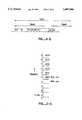
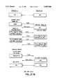
- FIG. A-1is a block diagram illustrating a communication network 10 based on a bus medium 12.
- Bus medium 12typically has the physical topology of a tree structure with a number of branches 12' to which various network nodes are coupled.
- the primary function of the network as described hereinis to support voice communication among users on the network and between such users and the public switched network.
- network 10may also be used for data and video as well.
- the networkcontains no central intelligence for allocating bus resource. Rather, each node has its own intelligence providing it the capability of vying for and claiming bus resource as needed.
- the network nodesinclude a plurality of voice interface units ("VIU's") 20, each shown with one associated telephone 22, a trunk interface unit (“TIU") 25 having a plurality of trunk lines 27 for coupling to the public switched network, an attendant interface unit/console (“AIU") 35, one or more network boot units (“NBU's”) 40, each with its associated non-volatile storage such as a hard disk 42, and one or more timing mark generators (“TMG's”) 45.
- Bus medium 12is coupled to a head end retransmission unit ("HRU") 50.
- An I/O processor (“IOP”) 51couples TIU 25 to HRU 50.
- a network manager workstation (“NMWS”) 52 with an associated hard disk 53is coupled to the NBU and its disk.
- a VIUmay be single-port device with one phone as shown, or may be a multiple-port device (up to 24 ports) with each port capable of supporting a phone.
- NBU's 40 and HRUare physically located within the same cabinet as TIU, and timing mark generator 45 is incorporated into NBU 40. Thus there are no separate enclosures for TMG 45, NBU 40, or HRU 50.
- Each nodehas associated address information. This includes a 6-byte physical unit address (“PUA”) which is a hardware embedded serial number unique to that node with respect to any other node in any network made by the same manufacturer. Uniqueness with respect to nodes made by different manufacturers can be guaranteed by agreement between the manufacturers or the establishment of a central PUA issuing authority.
- PUAphysical unit address
- Nodescan also be assigned a 2-byte local unique address ("LUA") by the network manager.
- LUAis unique with respect to other nodes at a given customer site. It is possible to address all nodes at the same time with a broadcast LUA having a hexadecimal value FFFF.
- Nodescan also be assigned a 2-byte system link extension ("SLE").
- SLEsystem link extension
- the same SLEmay be assigned to multiple nodes, thereby permitting group addressing.
- a node supporting multiple phonesmay have more than one SLE.
- Each nodecontains a 64-bit hash table for each of PUA, LUA, and SLE address comparison. Since there are more than 64 possible addresses, the hash table mechanism does not provide a unique selection, but rather a first-level filtering only. Additional address selection is carried out by higher level software.
- the SLE hash tablehas bits set for the multiple SLE's, the positions being determined as described above. Due to the lack of uniqueness, the number of bits set may be less than the number of SLE's.
- CIDconfiguration identifier
- RAMrandom access memory
- CID'sare created by the system administrator at the NMWS.
- a unit's phone extension numbercan be used as the CID but this does not necessarily need to be true. Since each phone needs a configuration, multiple-phone VIU's will have multiple CID's.
- a special CID(value 0) is used to identify a configuration that if loaded into a unit, limits the unit's operation to acquiring manually entered CID's.
- Bus medium 12is preferably a broadband coaxial cable capable of supporting a number of frequency channels, each defined by a carrier frequency on which signals can be superimposed. Each user device can broadcast its transmissions on the cable toward HRU 50. HRU 50 operates to receive signals on a first set of channels and retransmit them on a second set. Thus, two-way communications may be implemented on a single cable by frequency division multiplexing the available RF cable spectrum.
- the channelsare preferably 6 MHz wide, with the transmitting channels in the range from 5-108 MHz and the receiving channels in the range of 175-400 MHz. In the preferred embodiment, there are four channels, each with an associated transmit frequency and receive frequency band, and each node is capable of operating on any of the channels. Each node is assigned a home channel on which it normally listens when not participating in a communication. Boot transmissions typically occur on a designated boot channel.
- HRU 50transmits a pseudo-silence pattern (PSP) (e.g. alternating 1's and 0's) when there is no incoming data.
- PSPpseudo-silence pattern
- the PSPacts as a "not" carrier detect, and the VIU's may consider the given channel as free when the PSP is received.
- HRU 50implements a data reclocking scheme to provide a constant phase data signal to the nodes. Since the upstream transmission is supplied by an unknown source with regard to phase (since the relative phase of the incoming packets varies with the physical position of the originating node), HRU 50 uses a Maximum Likelihood Detector (MLD) to reclock the downstream transmission.
- MLDMaximum Likelihood Detector
- the MLDdetects the rising edges in the first four bits of packet preamble, and then delays the data path by a time of 0 to 1 bits (in increments of 0.062 bits) to properly align the center of the data bits and the edge of the sampling clock. With this method, no frequency lock is required since the downstream transmissions of HRU 50 are the system's source of master clock.
- the described functionscan be implemented with a high speed digital phase-locked loop that responds to the received packet's needs within a four-bit time span during the packet preamble.
- the selected delaywill remain locked until a loss of carrier is detected at the headend which will be interpreted as an "End of Packet”.
- HRU 50will then begin transmitting pseudosilence and reset the MLD for the next packet.
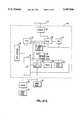
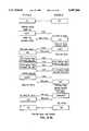
- network 10is physically and topologically organized as a tree, it is logically organized as a bus.
- the busis logically a dual linear bus having transmit and receive channels 55 and 57 as shown schematically in FIG. A-2. While only two VIU's and two NBU's are shown, an actual system might have a hundred or more VIU's.
- the representation of FIG. A-2is schematic only, since there are not actually two physical buses, but rather a single broadband communications medium capable of supporting a number of communication channels.
- FIG. A-3is a diagram showing the time structure of signals on the network.
- TMG 45provides a series of timing mark packets ("TM's"), transmitted simultaneously on all four channels, at 1-ms intervals, thereby defining a series of 1-ms frames.
- TM'salso indicate whether they are on a boot channel, and provide the channel number.
- the framesare logically grouped into pairs, each containing first and second frames, designated the forward frame and the reverse frame, with each pair defining a 2-ms cycle.
- Each frameconsists of a 10-byte timing mark, a 71-byte (60 data bytes) signalling packet ("SP"), and 28 19.5-byte (16 data bytes) voice timeslots ("VTS's"), each capable of containing a voice packet ("VP").
- SPsignalling packet
- VTS's19.5-byte (16 data bytes) voice timeslots
- Each packet intervalconsists of a preamble of alternating 1's and 0's, a delimiter, a data field, and a pad.
- the delimiteris a binary code specifying whether the packet is a TM, a VP, an SP, a claiming voice packet ("CVP"), or a boot packet ("BP”), and is distinguishable from the preamble in that any 3-bit string has at least two bits in a row the same.
- Table A-2provides a list of the various packet formats.
- VP'sare used to provide voice communication and contain binary encoded (pulse code modulation--"PCM") speech from a specific phone conversation. They are transmitted every cycle during the course of the conversation.
- An ongoing telephone conversationentails having VP's for one direction of the communication carried on a VTS of the forward frame and for the other direction of the communication on the corresponding VTS for the reverse frame.
- VP'scontain no computer recognizable information. They are merely reconstructed into voice at the receiving node.
- a special voice packet, the CVPis used to reserve a VP timeslot for data transmission/reception.
- SP'sare used for communications between nodes and contain computer recognizable information pertinent to the control of the network. While specific types of SP's will be discussed below, it is noted that an SP contains a data portion which includes a link header and a transport header as well as information specific to the type of SP.
- the link headercontains source and destination address information, specifically: 2 bytes of destination address information (enough for an LUA or an SLE); an address control byte containing two 2-bit codes specifying the destination and source address types (PUA, LUA, or SLE); a length byte; 4 bytes for the rest of the PUA if the destination address is a PUA; and 2 or 6 bytes of source address information.
- BP'sare used in boot operations to communicate configuration data and operating code from an NBU to other nodes. BP's are broadcast in the VTS's normally occupied by VP's.
- Each nodeis characterized by a skew time related to its physical position on the bus. Skew time refers to the differential propagation delays resulting from the fact that the different nodes are at different distances from HRU 50.
- the nodes most remote from the HRUwill receive the timing marks latest in time, and would, if they merely synchronized their transmissions to the timing mark, transmit relatively late compared to nodes nearer the HRU. Accordingly, the further a node is from HRU 50, the earlier it must transmit relative to the timing marks to be in synchronization. A procedure whereupon each node determines its own skew time is described later in this application.
- each nodeon power-up, transmits an SP immediately upon receiving a timing mark, and counts the number of bit times (1/(5.018 MHz)) until it receives the same SP (as retransmitted by the HRU). This defines twice that node's skew time, and subsequent transmissions will be advanced by the skew time.
- the TMG'sarbitrate amongst themselves at power up to determine which is to become the master TMG. Each TMG waits a random length of time (up to about 50 ms), and then broadcasts TM's on all channels. If a TMG receives TM's that it sent, it assumes the status of master TMG. The other TMG's assume the status of backup TMG's and monitor the four channels to ensure that the master TMG is sending valid TM's. In the event that TM's on any channel stop for some number of consecutive frames, the backup TMG's arbitrate to become the new master TMG. The arbitration process is similar to that described above.
- the hardware for a given node in the networkincludes certain portions that are essentially common to all nodes and certain portions that are different for the different types of nodes.
- the description in this sectionwill be in terms of one of VIU's 20 and one of NBU's 40.
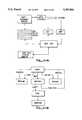
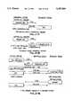
- FIG. A-4is a block diagram illustrating one of VIU's 20, the function of which is to interface one or more phones to the network.
- VIU 20like other nodes, must be able to communicate on any channel. Access to multiple channels (only one at a time) is provided by a frequency agile modem 70.
- VIU 20further includes a CPU 72 and associated memories, a codec 75 and telephone interface 77, and a control/interface circuit 80.
- nodes in the networkshare the same basic hardware organization in the sense of having the same control/interface circuit elements, CPU and associated memories, and modem. However, other types of nodes would not include codec 75 or telephone interface logic 77, and would have different operating software and configuration data stored in their associated memories. Some types of nodes (such as an NBU or a multi-port VIU) must be able to communicate on all channels at the same time, and are provided with a separate control/interface circuit and modem for each channel. Because each node uses the same basic set of network elements for all configurations, the network is modular and incrementally expandable for both small and large telephone systems.
- the memories associated with CPU 72include a packet RAM (“PRAM”) 2, a DRAM 85, and a boot ROM 87.
- Control/interface circuit 80contains a receiver/transmitter (“RxTx”) 90, a packet controller (“PCTL”) 92, a 3-port memory controller 93, and a PCM highway 95.
- PCM highway 95is a 1.544-MHz, serial, full duplex highway which provides 24 8-KHz 8-bit timeslots (much like a T1 carrier).
- a timing mark state machine 97shown in phantom since it isn't used in the VIU.
- control/interface circuit 80is implemented in a 2-chip set, one chip containing RxTx 90 and timing mark state machine 97, and the other containing PCTL 92, 3-port memory controller 93, and PCM highway 95.
- Table A-3provides a memory map of PRAM 82.
- the PRAMcontains, among other things, transmit and receive ring buffers for the PCM highway timeslots, tables specifying which network VTS's are free and which are busy, and boot buffers 100a and 100b.
- Three-port controller 93allows PRAM 82 to be accessed by RxTx 90, PCTL 92, and CPU 72.
- the 3-port controlleris responsible for arbitration and control of all PRAM accesses, including accesses to buffers in PRAM 82 that hold incoming and outgoing packets.
- RxTx 90provides a 5.018-MHz serial interface to modem 70. It is at this interface that VP's and SP's are communicated. A phase-locked loop in modem 70 recovers the system clock information (5.018 MHz in two phases) and provides it to RxTx 90.
- the RxTxgenerates transmit and receive frame boundaries and the timeslot boundaries within each of the frames. In most cases it uses its received frame as the time base and starts its transmit frame a skew time before.
- RxTx 90is also responsible for skew calculation, preamble insertion and removal, and delimiter insertion, removal, and recognition. RxTx 90 also interfaces to CPU 72.
- PCTL 92operates under control of RxTx 90 and is responsible for voice and tone buffering and routing between network 10 and PCM highway 95.
- PCTL 92also supports tone generation (dial tone, ring back, DTMF).
- tone generationdial tone, ring back, DTMF
- control/interface circuit 80A key function of control/interface circuit 80 is to route VP's, and to that end must keep track of the active VTS's on the network and map each of these active VTS's to one of the 24 voice ring buffers in PRAM 82.
- the ring buffersare then mapped one-to-one to the 24 PCM bus timeslots in order to establish a connection between the network VTS and the codec.
- For receiving data RxTx 90removes the preamble and delimiter, performs a serial to parallel conversion, and passes the data to PCTL 92.
- the PCTLstores the data in the ring buffer and sends bytes to the codec as required.
- the ring bufferscontain only the actual voice samples for VP's or boot data for BP's.
- the PCTLreceives PCM data samples from the codec, and stores them in the PRAM ring buffer.
- the PCTLthereafter provides the appropriate address information to RXTX 90, which appends a preamble and delimiter, performs a parallel to serial conversion, and transmits the data onto the network.
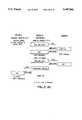
- FIG. A-5is a block diagram illustrating one of NBU's 40, the function of which is to download boot images (configuration data and operating software) to other nodes, referred to as boot consumers.
- NBU 40shares many common circuit elements with VIU 20 (and other nodes in the network).
- the NBUcontains those elements described in connection with FIG. A-4 except codec 75 and telephone interface logic 77. While the NBU does not support telephones, it includes and uses the PCM highway to support conference calls. Those elements that do correspond are shown with the same reference numerals. Since, in the current implementation, timing mark generation is actually carried out by the NBU hardware, the NBU has four control/interface circuits and modems so as to be able to transmit TM's on all four channels simultaneously.
- the NBU's CPU 72interfaces with the NBU's associated hard disk 42 through a small computer system interface (SCSI bus interface) 105.
- the boot imagesare developed in an off-line development system and written onto floppy disks, which are loaded into NMWS 52 and stored on the NMWS hard disk. The boot images are then transferred to the NBU hard disk(s) independently of the network.
- Each NBUwill typically have boot images for all of the nodes in the network.
- the software in a given nodeis organized in a layered structure based on the International Standards Organization ("ISO") Open System Interconnection Reference Model (“OSI”).
- ISOInternational Standards Organization
- OSIOpen System Interconnection Reference Model
- the OSI modelcontemplates an organization having some or all of the following layers:
- the physical layeris concerned with the interaction between the nodes and the network communications medium.
- the physical layerencompasses the modem and cable.
- the link layersupports communications between nodes on the network, and is implemented using both hardware (most notably control/interface circuit 80) and software.
- the link layer functionsare as follows: monitoring TM reception for all nodes and supporting TM generation on certain devices; best effort delivery of SP's; selective filtering and verification of incoming SP's (using the hash tables); supporting boot buffer transfers; establishing, monitoring, and disconnecting voice circuits; transferring voice (with padding) from network to the codec; and transferring voice from the codec to the network; generating tone to the codec (with padding) and/or to the network; generating silence to the codec; performing diagnostics and reporting severe errors; and presenting statistics and minor errors gathered by the hardware.
- the network layerprovide a (channel) bridge for establishing communication between channels on the same cable, and between different cables, and will not be discussed further.
- the transport layeris responsible for the reliable end-to-end delivery of data between host entities. This includes providing both best-effort and reliable datagram transfer services, built upon the service exported by the link layer.
- transportmakes a best effort to deliver an information (or a response) packet to the destination(s), but will not notify the requesting session entity if the delivery is not successful.
- a "reliable" datagram deliveryentails delivery of a user information packet to the destination(s), with notification to the requesting session entity if transport is unable to deliver the packet.
- Transportalso supports large data deliveries wherein a large data transfer request from a user entity is delivered to the destination(s) using a combination of both pure and reliable datagrams. If transport is unable to deliver the entire data without error, it will notify the requesting session entity.
- Appendix 1is a specification for the transport layer software, setting forth the different transaction types supported.
- the OSI modeldescribes the session layer as the level that provides services required to establish and maintain connections between users across the network. It provides the following services: call establishment and disconnection functions between stations connected to a local area network; initiation and monitoring the voice communication path between the station set users; call establishment and disconnection functions for establishing voice communication between station users and the public switched network users; and implementing various end user features.
- the session layerhas to provide different types of services to the higher layers. While it is possible to provide a common base code to some extent, the differences between such units as VIU's and NBU's make it difficult or impossible to use the same session software on these different types of nodes. However, all the nodes utilize the same set of services and interfaces provided by the lower layers.
- the presentation layeris in general concerned with the user interface. With respect to the network software running in the VIU's, the presentation layer is concerned with the duration and format of all the tones a user may hear from the handset, as well as controlling keyboard interaction and the format of messages displayed on liquid crystal displays for those phone models so equipped. A substantial part of these functions is actually implemented in hardware.
- the presentation layeris limited to tone generation and detection.
- the presentation layer functionsare really incorporated in the NMWS.
- the application layeris in general concerned with the user application.
- the only application level software implementedis the Network Manager.
- the Network Managerperforms the following functions: node configuration, downloading of configuration and code images to the network; monitoring, display and storage of network events; network diagnostics; automatic route selection table generation; and remote network diagnostics.
- the software for certain nodescontains additional code to control the communications across the interface.
- Appendix 2is a specification of the software in the DRAM for controlling the communications.
- Appendix 3is a specification of the firmware for "Spike.”
- All other stations on the networkreceive the Call Request SP and compare the contents of the destination field within the packet to the extension numbers which are supported by the receiving station. The Call Request is ignored if no match exists. If the destination extension matches one of the extensions supported by the receiving station, and the destination is not busy, the destination sets itself to operate on the originator's home channel, after which an Accept SP is sent back to the originator with the receiving station's LUA.
- an Accept Acknowledgement SPis sent directly to the accepting station using LUA addressing to begin ringing at the destination station, and a ringback tone is sent to the originator's handset.
- the reverse timeslotis claimed, indicating an answer.
- an Answer SPis returned to the originating station.
- Silence VP'sare now replaced with actual VP's.
- a Disconnect SPis sent by the terminating station and the connection is terminated. If the destination is busy, a Busy SP is returned to the originator and the exchange ends with the originator receiving a busy tone.
- Nodesrequire the downloading of boot images when they are powered up, which occurs after a power failure, when they are first brought on line, or when they are disconnected and moved. Boot images are also downloaded when a new software release is to be installed on some or all of the nodes. Downloading typically occurs in two stages, first program code, and then configuration data. The program code is generally much longer than the data, and can be downloaded to a number of nodes at the same time. The configuration data is different for each node, and must be downloaded on an individual basis. As will be described below, a node, having received its code image requires its CID before it can request its configuration.
- Table A-4provides the format of a boot image file. Boot images are divided into blocks, with the size of each block depending on the size of boot buffers 100a and 100b in PRAM 82 (256 bytes each in the present implementation). As can be seen, the file contains an initial block having global information as to the boot image file, and a number of data blocks, each having the actual data and associated header information about the specific block (load address, block size, block number).
- BP'swhich occupy VTS's, are used to transmit boot images over the network.
- Each BPcontains 16 bytes of data, which translates to a data rate of 64 kilobits/sec if only one VTS per cycle is used.
- BP transmission and receptionmay occur on multiple VTS's, thereby providing higher data rates.
- Boot transmissionsoccur in response to requests from boot consumers. Such requests are typically made when a node is powered up, either at the same time as the rest of the network, or after being connected to the network while the rest of the network has been running.
- a node requiring a boot imagetransmits a boot request SP ("BRSP") to request the image it needs.
- the NBUresponds by sending boot control SP's ("BRSP") and BP's, as will be discussed in detail below.
- Table A-5sets forth the format for a BRSP.
- BRSP'sare'sent to an address permanently assigned to NBU's and contain image descriptor information specifying the memory image being requested.
- Table A-6sets forth the format of a BCSP.
- BCSP'sare sent on all channels and contain boot control and image descriptor information.
- Boot controlspecifies which channel, frame, and VTS('s) are used to transmit the image.
- the image descriptorprovides information about the memory image itself. This information is statically bound to each boot image and resides with the boot image on hard disk 42. It is generated in the development environment and included as the header of the boot image file. It is extracted by the NBU to create the BCSP.
- FIG. A-6is a flowchart of the boot ROM code.
- the nodescans the various receiver frequencies to find a channel with timing marks. After identifying its unit type and boot channel, the node begins to receive and interpret SP's, waits for BCSP's identifying the necessary image, and transmits a BRSP if it does not receive the required BCSP within a certain random time interval (up to 50 ms). It performs its part of the boot operation according to the parameters specified in the BCSP.
- FIGS. A-7A and A-7Bare flowcharts of the NBU code.
- the NBUclaims one or more VTS' (in the same manner as the VIU claims a VTS in a voice call), and transmits (on all channels) boot control SP's ("BCSP's") containing boot control information and image descriptor information about the boot image being broadcast.
- BCSP'sboot control SP's
- each NBUUpon receiving a BRSP, each NBU attempts to claim the service by adding the boot group address of the requested image and sending a BCSP with no VTS's allocated. If it receives its own BCSP (as determined by the source address) first, it will start the boot process by claiming one or more VTS's and sending a BCSP to the boot consumers. The downloaded image will satisfy multiple requests for the same image.
- BCSP'sare sent a predetermined amount of time before the actual transmission of the specified block so as to allow the boot consumers time to receive the image. They are also sent throughout the image transmission to allow other boot consumers to start receiving the image in the middle of the transmission, with a second transmission being used to fill in the missing parts.
- BCSP'sare sent to group addresses, there being a group address assigned to each type of network unit. Boot ROM 87 in each unit, based on its unit type, can receive and filter for the corresponding BCSP.
- NMWS 52causes the NBU to send an SP instructing nodes to take themselves out of service and then to come back up.
- the nodesrequest the boot images as discussed above.
- Boot packetsare sent from and received into boot buffers 100a and 100b in PRAM 82.
- the control/interface circuitalternates between the boot buffers when retrieving or storing boot information, varying the delimiter to specify which buffer is to be used.
- the boot registersare typically zeroed by software before starting boot transmission or reception. PCTL 92 controls (writes to) these registers during the boot process, so software should not write to the boot registers while the boot operation is in progress.
- the Tx boot buffer registerspecifies the boot buffer (0 or 1) from which the next BP is to be fetched.
- the Tx boot pointer registerpoints to the location in that boot buffer of the next BP.
- the Tx boot buffer registeris toggled immediately after the last byte in a given buffer is read by PCTL 92.
- the Rx boot buffer registerpoints to the boot buffer (0 or 1) to which the next received BP is expected to be delivered.
- the buffer into which it is actually placeddepends on the BP delimiter.
- the Rx boot buffer bytetoggles after a BP is received which fills the current buffer, or immediately upon reception of a BP destined for the other boot buffer.
- the Rx boot pointer registeralways points to the next byte in the current boot buffer into which a BP is to be written.
- the VIUthen uses this zero value CID to get a special configuration that only allows CID entry from the phone; no phone calls are possible with this configuration.
- a user picking up the handsethears an "Enter CID" tone instead of a dial tone.
- the usermust then invoke the feature code to enter a CID, and hears no tone until the CID is verified.
- the VIU softwarereceives the CID, and sends a CID Request SP (with the non-zero CID) to register the CID with the NBU.
- the NBUresponds with a CID Response SP that contains the CID.
- the VIUgives a "CID Confirmed" tone to the user.
- the networkalso supports de-registration and re-registration of nodes according to pre-configured criteria.
- Appendix 4is a detailed specification of procedures for registration and de-registration of Voice and Trunk Interface Units. Varying modes of registration and re-registration are permitted. Thus, global registration and re-registration permits new phones to be added and existing phones to be re-registered at will, while the most secure mode permits nothing to be registered or re-registered.
- FIG. B-1is a more detailed diagram of RXTX 90.
- RXTX 90comprises a modem interface 120, a modem receive state machine 124, a modem transmit state machine 128, a CPU interface 132, and a PCTL interface 136.
- RXTX 90is synchronized to the network and therefore requests network-related data transfers.
- Modem interface 120packetizes and depacketizes all information going through control/interface circuit 80. This includes inserting/detecting delimeters and generating/checking CRC's. The low level tasks of determining skew and maintaining the receive and transmit frame timing are also done here.
- CPU interface 132consists of interupt circuitry, command and status registers, and the microprocessor interface circuitry required to access them.
- CPU interface 132is designed to interface with the intel 80186 bus structure. To minimize the real-time load on CPU 72, CPU 72 is interrupted only when an event in which it is interested occurs.
- PCTL interface 136takes care of any buffering or timing considerations that might be necessary for receiving and transmitting data. PCTL interface 136 also communicates the necessary information with PCTL circuit 92 for accessing P-RAM 82. In this embodiment, PCTL interface 136 is directly coupled to the P-RAM 82 data bus.
- Modem RX state machine 124 and modem transmit state machine 128control the operations between modem interface 120, CPU interface 132 and PCTL interface 136.
- the operation of modem receive state machine 124 and modem transmit state machine 128is governed by the timing inputs from modem interface 120 and the commands received from CPU interface 132.
- Modem receive state machine 124 and modem transmit state machine 128interact with each other when a node is monitoring its own transmission (e.g. CVP's).
- FIG. B-2is a more detailed diagram of PCTL circuit 92.
- PCTL circuit 92includes a RXTX interface 142, a network receive state machine 146, a network transmit state machine 150, a P-RAM interface 154, a PCM highway interface 158, a PCM highway state machine 162, and a CPU interface 166.
- RXTX interface 142is responsible for accepting commands from RXTX 90 and passing them to the appropriate network state machine 146 or 150. RXTX interface 142 also keeps track of the current network transmit and receive timeslots via network transmit and receive framing signals from RXTX 90.
- Network receive state machine 146translates the commands received from RXTX 90 involving network receive operations into the appropriate P-RAM 82 accesses. For example, one of these commands instructs network receive state machine 146 to deliver voice data to the P-RAM resident receive ring buffers from RXTX interface 142.
- Network receive state machine 146is responsible for generating the required P-RAM addresses and for controlling the data flow between P-RAM 82, PCTL interface circuit 154, and RXTX interface 142. In addition, it maintains all state information necessary to perform these tasks, such as pointers into the TM, SP, CVP, and BP receive ring buffers.
- Network receive state machine 146uses its own time slot interchange table to read the mapping between the network receive time slots and the receive ring buffers.
- Network transmit state machine 150translates commands from RXTX interface 142 involving network transmit operations into appropriate P-RAM 82 accesses. For example, one of these commands instructs network transmit state machine 150 to deliver voice data from the P-RAM resident transmit ring buffers to RXTX interface 142.
- Network transmit state machine 105is responsible for generating the required P-RAM addresses and controlling the data flow between P-RAM 82, PCTL interface 154, and RXTX interface 142. In addition, it maintains all the state information necessary to perform these tasks, such as pointers into the TM, SP, CVP, and BP transmit ring buffers.
- the network transmit state machine 150interprets the P-RAM resident time slot interchange which maps the network transmit time slots to the appropriate transmit ring buffer (and thus PCM highway timeslot). It then controls the actual data transfers from the P-RAM resident ring buffers to RXTX interface 142.
- PCM highway interface 158is responsible for keeping the PCM highway state machine 162 in sync with the PCM highway. It also controls transmissions onto the PCM highway. Data transmitted on the PCM highway should be encoded using mu-255 as per CCITT recommendation G.711.
- PCM highway state machine 162is responsible for transferring data between the P-RAM 82 ring buffers and PCM highway interface 158. As discussed below, there is one transmit and one receive ring buffer in P-RAM 82 for each of the 24 PCM highway time slots to buffer voice data between the network and the codecs. PCM highway state machine 162 interprets the mode command register in P-RAM 82 that selects idle, voice, or tone mode, and then transfers information as required. PCM highway state machine 162 also checks both transmit and receive ring buffers in P-RAM 82 on every access for overflow conditions, and takes appropriate action.
- P-RAM interface 154controls all accesses to P-RAM 82. It uses a slotted access scheme, reserving every other P-RAM access for PCM highway state machine 162. It reserves the remaining access slots for network transmit state machine 150 and network receive state machine 146 as shown in FIG. B-3. Each state machine must request each use of its access slots from P-RAM interface 154. Any slots not used by their owner are available for use by CPU 72.
- CPU interface 166services CPU requests to read from or write to command and status registers disposed within CPU interface 132. In addition, it routes requests to read from or write to P-RAM memory space to P-RAM interface 154. P-RAM interface 154 in turn provides a "ready" signal to CPU 72 when appropriate and transfers data as required. As the CPU operates using an unknown clock phase (and possibly frequency) compared to RXTX 90 and PCTL 92, all CPU requests are synchronized to the clocks within RXTX 90 and PCTL 92 before being executed.
- FIG. B-4is a more detailed diagram of the inputs and outputs for RXTX 90, PCTL 92, and P-RAM 82.
- the I/O terminals of modem interface 120 (FIG. B-1) in RXTX 90includes an M-5 input terminal 200 for receiving 5.018 megahertz clock pulses (used e.g.
- an RXD input terminal 204for receiving serial data (5.018 MBPS) from modem 70; a TXD output terminal 208 for transmitting serial data (5.018 MBPS) to modem 70; an ME output terminal 212 for providing a modem enable signal to modem 70; a RCH bus 216 for providing a 4-bit receive channel number to modem 70; a TCH bus 220 for providing a 4-bit transmit channel number to modem 70; an MF input terminal 224 for receiving a modem fault signal from modem 70; a MFR output terminal 228 for providing a modem fault reset signal to modem 70; an OSCE output terminal 232 for providing an oscillator enable signal; and a bidirectional M/SF terminal 236 for synchronizing the transmit frame with other RXTX circuits 90 at the node.
- M/SF terminal 236is an output terminal when RXTX circuit is a master timing mark generator, and it is an input terminal when RXTX circuit 92 is a slave timing mark generator. Circuit timing will be
- the I/O terminals of CPU interface 132 (FIG. B-1) in RxTx 90include a bidirectional RTCPUD 242 bus for communicating 8-bit parallel status and command data with CPU 72; a RTCPUA bus 246 for receiving 5-bit addresses from CPU 72; an RTCS input terminal 250 for receiving a chip select signal from CPU 72; an INT output terminal 254 for providing interupt signals to CPU 72; an RDY output terminal 258 for providing "ready" signals to CPU 72; a BER output terminal 262 for providing bus error signals to CPU 72; an RTCPUR input terminal 266 for receiving CPU read pulses; and an RTCPUW input terminal 270 for receiving CPU write pulses.
- a bidirectional RTCPUD 242 busfor communicating 8-bit parallel status and command data with CPU 72
- a RTCPUA bus 246for receiving 5-bit addresses from CPU 72
- an RTCS input terminal 250for receiving a chip select signal from CPU 72
- an INT output terminal 254for providing interupt signals to CPU 72
- the I/O terminals for PCTL interface 136 (FIG. B-1) in RXTX 90, and RXTX interface circuit 142 (FIG. B-2) in PCTL 92include a TXS terminal 274 for communicating transmit frame synch pulses to PCTL 92 for marking transmit time slot boundaries; a TXFR terminal 278 for indicating to PCTL 92 whether the transmit frame is forward or reverse; an RXS terminal 282 for communicating receive frame synch pulses to PCTL 92 for marking receive frame time slot boundaries; an RXFR terminal 286 for indicating to PCTL 92 whether the current receive frame is forward or reverse; an RFL terminal 290 for indicating to PCTL 92 whether the receive frame is locked; a PW terminal 294 for providing signals to enable RXTX 90 to communicate directly with P-RAM 82; a synch terminal 298 for providing signals to synchronize the state machines within PCTL 92 with the state machines within RXTX 90; a 5-bit CMD bus 302 for communicating RXTX 90 commands to PC
- PD bus 136is coupled to one port of 3-port controller 93.
- the terminalsbay be broadly described as an interchannel bus (ICB).
- the I/O terminals of CPU interface 166 (FIG. B-2) in PCTL 92include a bidirectional PCPUD bus 320 which communicates with the lower 8 bits of the 80186 data bus; a PCPUA bus 324 for receiving the address bits required to access PCTL internal registers and P-RAM 82; a CRS input terminal 328 for receiving signals indicating that CPU 72 is accessing P-RAM 82; a CPS input terminal 332 for receiving signals indicating that CPU 72 is accessing the PCTL 92 internal registers; a CRD input terminal 336 for receiving the CPU read signal; a CWR input terminal 340 for receiving the CPU write signal; a CRDY output terminal 344 for indicating to CPU 72 that the PCTL 92 internal register or P-RAM 82 access requested by CPU 72 has completed and valid data is available or has been accepted; and a PBER output terminal 348 for indicating that the PCTL 92 access requested by CPU 72 has not completed in a timely manner,
- the I/O terminals of PCM highway interface 158 (FIG. B-2) of PCTL 92include an RPCM terminal 360 for transmitting data to codec 75; a TPCM terminal 364 for receiving data from codec 75; a PCLK input terminal 368 for receiving a 6.176 megahertz clock used to control the PCM highway interface; and a PCLK terminal 372 for establishing the 1.544 megahertz clock used to transmit and receive data on PCM highway 95.
- the signals on PCLK terminal 372are output by PCTL 92 when a "PCM highway master" bit is set in a PCTL mode register discussed below.
- PCM highway interface 158further includes a TSO terminal 376 for indicating that the PCTL 92 internal PCM highway time slot counter should be reset to time slot 0 on the next 6.176 megahertz rising clock edge.
- the signals on this lineare output by PCTL 92 when a "PCM highway master" bit is set in the PCTL mode register.
- a TXEN terminal 380provides signals to codec 75 indicating it should begin transmitting data on a current time slot; and a TOE terminal 384 provides signals to codec 75 to cause codec 75 to enable its output drivers to PCM highway 95.
- the signals on TOE terminal 384typically are required when using codecs which cannot generate the required transmit PCM highway time slot timing using only the signals on TXEN terminal 380.
- a RXEN terminal 388provides a signal which informs codec 75 to receive data from the PCM highway in a current time slot.
- a PTS bus 292provides the current 5-bit time slot number on the PCM highway.
- a 4-bit PST bus 396provide the current state of the PCM highway state machine. It is primarily used during chip test.
- the I/O terminals for P-RAM interface 154 (FIG. B-2) in PCTL 92include a 16-bit PA bus 402 for addressing P-RAM 82; a PCS terminal 406 for providing a chip select signal to P-RAM 82; a PWE terminal 410 for providing a write enable signal to P-RAM 82; and a POE terminal 414 for providing an output enable signal to P-RAM 82. These terminals are coupled to one port of 3-port controller 93.
- control/interface circuit 80functions, and to understand the organization of P-RAM 82 and the command/status registers in RXTX 90 and PCTL 92, it is helpful to list the commands which occur within control/interface unit 80. These commands may be separated into three categories: network commands processed by RXTX 90, PCM highway commands processed by PCTL 92, and RXTX/PCTL commands for communication between RXTX circuit 90 and PCTL circuit 92.
- TX TMTransmit timing mark
- TX SPTransmit signalling packet
- TX CVPTransmit claiming voice packet
- TX VPTransmit voice packet
- TX BPTransmit boot packet
- Receive boot packet(RX BP).
- P-RAM 82is organized as follows. As noted in Table A-3, the addresses are listed in hexadecimal. The numbers in parenthesis following the block definition is the number of bytes in the block.
- P-RAM 82contains not only the ring buffers used for transmitting the actual data between codec 75 and modem 70, but a number of command and status byte locations. The following tables and descriptions provide the bit assignments for the latter.
- the command number and a short descriptionis stated.
- the data fielddescribes what should appear on the PRAM data bus as a result of the command.
- the source and destinationtells where the data comes from and which devices use it.
- Source: PD ⁇ 7 . . . 0>is tri-stated.
- the Commandswill be NOPs (Command 0) until the Rx frame is locked (i.e. the TM threshold is reached).
- the following commandsare specifically for the transmit or receive direction.
- Read Net Tx Read PointerThis register holds the Xmt Ring Buffer address which points to the first byte to be transmitted in this time slot.
- Data FieldThe data byte to be transmitted in the current packet.
- Read Net Rx Write PointerThis register holds the Rcv Ring Buffer address where the first data byte is stored. When issued during a TM or SP time slot, the TM or SP pointer is just cleared since these packets always start at the same buffer address.
- the RxTxsends status to the PCTL, stating the type of packet that was received.
- Data FieldThe data byte received in the current time slot.
- the RxTxsends status to the PCTL, stating any errors detected after the entire packet has been received.
- CPU 72Upon initialization, it is necessary to establish system timing. To do this, CPU 72 sets the M/S bit in the TM Master/Slave Register (Table B-22) for each control/interface circuit which CPU 72 desires to be a potential TMG. Each potential TMG waits a random length of time (up to about 50 milliseconds) and then its timing mark state machine transmits TM packets on all channels.
- Table B-22TM Master/Slave Register
- the time periodrefers to the current octet on the node input (not the octet on the ICB). Also note that the commands in some delimiter time periods are labeled “early,” “late,” or “normal.” An “X” means either a 0 command or no command at all is sent (the delimiter or pad time period was curtailed).
- Tx time slotsstart during the pad of the previous time slot.
- the time slot counters in the RxTx chip and PCTL chipare incremented (using the signal on ync Terminal 298).
- the Tx state machineis allowed two commands for every octet. Since all pads except TM pads are 12-bits wide, there can be up to 3 commands during these times.
- a control/interface circuit 80receives the TM packet that it sent intact, it assumes the status of master TMG. The other control/interface circuits clear the M/S bit, assume the status of slave TMGs, and monitor their respective channels to ensure that the master TMG is sending valid TM packets.
- each control/interface circuit 80must establish proper receive and transmit frame timing. This is done by first capturing and locking into the incoming TM packets. Both master and slave TMGs perform this function. After coming out of reset or after the TM window bit in TM Command/Lock Status register (Table B-23) is set to zero by CPU 72, RXTX 90 will begin searching continuously (i.e. the search window is "wide open") for good TM packets. During this time, no other packets are recognized. It is possible to detect several good TM packets within a millisecond, since there may be different devices arbitrating to become the master TMG. Errors will be recorded to prevent a false lock.
- RXTX 90will lock the incoming frame by setting the TM Window bit to one. This means that RXTX 90 will search for TM packet delimiters during a small window at a predicted time (every millisecond). This leaves the rest of the frame for servicing other packets, and RXTX 90 can function normally. Furthermore, looking for TMs only when they are expected prevents occasional voice data which mimic TMs with valid CRCs from causing receiver synchronization malfunction.
- CPU 72sets the "TM lock threshhold" in the TM command register (see Table B-23) to determine how many consecutive good TM packets must be detected before the frame is locked.
- RXTX 90will lock the frame automatically when this threshhold is reached. If the chosen threshhold is too long, CPU 72 can lock the frame manually by setting the TM Window bit to one. In this embodiment, RXTX 90 cannot automatically declare loss of frame and open the search window by itself to reestablish it. Even if several frames have passed without good TM packets, RXTX 90 must continue to predict frame boundaries until the device is reset or CPU 72 gives an explicit command to open the window.
- the receive frameis established upon reception of the next good TM packet.
- RXTX 90counts the number of bits of the TM pad time and creates a bit-wide pulse during the last bit of the TM pad. See FIG. B-5. A number of bits in an SP is then counted, and the first voice time slot is marked by a pulse. This continues until the next TM time slot where the pulse is lengthened to 8 bits to mark the beginning of a new frame. Once the receive frame is locked, the receive frame time pulses are meaningful. These timing pulses are shared with PCTL 92 (via RXS terminal 282) and allows control/interface circuit 80 to receive information within distinct time slot boundaries.
- the beginning of the SP time slotis determined from the last good TM packet. That is, RXTX 90 continues predicting time slot boundaries even if the TM packet is bad.
- a separate signalindicates whether the present frame is forward or reverse. This is determined by the LSB of the received frame number of a good TM packet (in this embodiment, if the TM packet is bad, the signal is toggled). This signal will be valid after the TM CRC is checked for the SP time slot.
- the pulses of the receive frame signalsmark the predicted time of arrival of a preamble.
- a packetmay arrive four bits earlier or later (because of reclocking by HRU 50). Because of this, a 16-bit window is established in which the delimiter may be found. See FIG. B-6. A delimiter that lies partly or wholly outside this window must be ignored so that neighboring time slots are not affected.
- the TM and VP slotsuse 16-bit windows.
- the SP slotsuse 16-bit windows also unless the SSP is expected.
- the pulse for the next time slotdoes not change if a delimiter of the current time slot is early or late. This is because the source of transmission of the next time slot is independent.
- the shift in timing caused by an early or late delimiteris absorbed by the preamble or the pad (one or the other is shortened).
- the Tx framemust start a skew time before the Rx frame. Therefore, before Tx frame timing may be established, skew must be calculated. This is done by transmitting and receiving a skew signalling packet (SSP).
- SSPskew signalling packet
- the skewis represented by the number of bit times (of the 5.018 Mhz clock) it takes for the round trip delay.
- skew for a particular deviceis recalculated every time it sends an SP.
- a Signalling Packetis sent out during the SP timeslot, according to the SP Space and Tx Channel bits of the command.
- this transmitted packetis received and the CRCs of each are calculated and compared to detect collisions.
- An interruptis given after this receive check is performed giving the results.
- the hardwareclears the command after the packet is transmitted to ensure the same packet is not transmitted again.
- All SPs transmittedare either 14 bytes long or 60 bytes long from the end of the delimiter to the start of the CRC (i.e. control/interface circuit 80 always transmits one of these lengths).
- the short packetsare used to set the skew so that they do not interfere with the first voice timeslot if the actual skew of the control/interface circuit is great.
- the maximum length packetsare used at all times thereafter.
- a new skew calculationis performed whenever a Tx SP command is given by CPU 72.
- the new valueis only accepted by control/interface circuit 80 if the SP was received correctly.
- RxTx 90will generate and send a CRC after the 14th byte of an SSP.
- the Tx modemwill be disabled after the CRCs are sent, but the command sequence will continue as if a regular SP is being processed. All commands issued after the SSPs CRC are ignored.
- SPsare placed in eight different partitions in this embodiment.
- the partitionsare determined by a modulo eight frame counter (modulo four cycle counter) transmitted by the master TMG.
- CPU 72specifies, via the SP command register, in which one or more of the eight partitions it can be sent.
- RXTX 90then transmits the SP on the next allowable frame.
- This partitioning schemeis simple enough to be implemented in hardware, thus freeing CPU 70 for more important tasks.
- Control/interface circuit 80will receive any SP sent on the channel to which it is listening, except when that control/interface circuit is transmitting an SP on another channel during that frame.
- the receive sequence for SPs and SSPsare the same except for the length of the data byte field.
- the RxTxwill know if it had just sent an SSP because it will have set the TX SSP bit in the SP Status Register. Since the SSP is much smaller in length than an SP, it may be received in a much larger window during the SP time slot. Because of this, there may be a long sequence of NOPs (Command 0) when waiting for the arrival of an SSP packet.
- the Tx frameis generated two different ways depending on whether control/interface circuit 80 is a master TMG or a slave.
- the start of the Tx framedepends on when the TM was received and the length of the skew.
- the Tx and the Rx framesare independent.
- Slavesare all control/interface circuits except for the device that is a master TMG.
- the Tx framemust start a skew time before the Rx frame.
- the control/interface circuitneeds to know the beginning of the Rx frame to establish the beginning of the Tx frame.
- One way to circumvent this dilemmais to establish the beginning of the next
- Each Rx frameis given a frame number by the master TMG.
- the Rx frame with frame number Nwill establish the beginning of the Tx frame with frame number N+1 (See FIG. B-7).
- the beginning of the TX frameis determined by counting down from a fixed point in the Rx frame until this counter equals the skew count register. This fixed point must be far enough from the end of the Rx frame so that the maximum possible skew that the system will tolerate can be supported. This point is thus called the maximum skew point or MSP.
- the time slot boundaries of the Tx frameare slightly different from that of the Rx frame. Instead of starting during the last bit of the previous packet's pad time, the pulse occurs at the beginning of the pad time. This allows RxTx 90 to prepare for data transmission well before the upcoming preamble (See FIG. B-8).
- a control/interface circuitis the Master TMG or if it is contending to become the TMG (during power up or the loss of the Master TMG), the start of the Tx frame is independent of the Rx frame. The start of the Tx frame is dependent, however, to the start of the Tx frame of other TMGs in the system.
- the control/interface circuitscan work by themselves, but in this embodiment, all TMGs are synchronized (via the C-M/S bit in the TM Command/Lock Status register (Table B-23) and SYNC terminal 298) so that transmissions of TMs occur simultaneously.
- the pulses for the Tx frame during Master Modeis the same as for Slave Mode. That is, the beginning of a time slot is marked by a pulse at the beginning of a previous time slot's pad time.
- Rx timingdiffers from Tx timing in that Rx time slot boundaries are predicted values. Frame boundaries are aligned after receiving a good TM, but since each time slot contain information from varied sources, the first byte of the packet, the preamble, may actually appear 4 bits earlier or later than the predicted time slot boundary. (The theoretical limit for error is plus or minus 2 bits, but the RxTx chip will accept up to plus or minus 4 bits of error).
- a time slotcan receive a packet 4 bits earlier than predicted. Since the time slot counter changes at the predicted preamble time, half of the preamble time will have already passed if a packet comes early. This, effectively, allows for only one command during the preamble time. If the preamble is late by (worst case) 4 bits, there may be up to three commands during the preamble.
- the PADis affected also. If the packet is late the pad time is shortened; hence, there may be only two commands instead of three during the 12 bit pad of voice time slots and only one command instead of two for the 8-bit pads of TM and SP time slots. If the packet is early, the pad time is lengthened; hence, there may be up to four commands during voice time slot PADs and up to three for TM and SP PADs.
- the CVP command registeris used to determine if there will be CVP transmission in the present time slot.
- the commandinstructs control/interface circuit 80 to send a single VP out on the selected VP timeslot and check the transmission coming back to detect collisions. If this one shot packet is transmitted and received with no errors, this unit has successfully claimed the selected VP timeslot, and can set up a normal Tx VP command. If not, the unit can try to claim another timeslot.
- the control/interface circuitchecks the selected VP timeslot's busy/free table entry before sending the CVP (during SP processing) to eliminate race conditions on a claim. If it is found to be already busy, the control/interface circuit inhibits the CVP transmission, sets a status bit, and reports this condition via an interrupt. If the claim was actually sent, the busy/free entry is left free. This allows units involved in CVP collisions to arbitrate between themselves for the timeslot. Other units will not be able to claim the slot as their busy/free tables will indicate that the timeslot is busy. This feature is especially useful for multiple responders.
- RxTxneeds to remember the transmit time slot to send the CVP (n) and the receive time slot to check it (n+1). If the CVP is transmitted, it is received and its status reported with an interrupt. The possible conditions are successful claim (Rx'd packet matched Tx'd packet), collision detected, or nothing detected.
- This commandgiven via the Tx Active Table entry for the selected voice timeslot, instructs control/interface circuit 80 to transmit 16 bytes of voice data onto the network during this timeslot each cycle. It gets this voice data from the P-RAM via PCTL 92, which has been previously set up by CPU 72 to deliver data from the correct PCM Highway timeslot or tone buffer.
- This commandgiven in the Receive Active Table entry for the selected timeslot, instructs RxTx 90 to receive incoming packets during this timeslot and transfer them to P-RAM 82 under control of PCTL 92.
- PCTL 92has been previously set up by CPU 72 (through P-RAM) to deliver data to the correct PCM Highway timeslot receive ring buffer.
- Tx BPBoot Packet
- This commandgiven via the Transmit Active Table entry for the selected voice timeslot (and enabled via a boot mode bit), instructs control/interface circuit 80 to send the next 16 bytes of the currently selected boot buffer (0 or 1) out during this timeslot, using the corresponding boot delimiter. If this 16 bytes completes the buffer, control/interface circuit 80 will automatically switch to the other buffer, set status bits, and interrupt the CPU.
- This commandis implemented via a normal Tx VP command, combined with the active/idle bit in P-RAM's Network Transmit--PCM Timeslot Map Entry for the timeslot.
- the Codec State Machineis responsible for the following:
- Voice data from the network and tones destined for the codec buscan be attenuated or amplified as desired via a digital pad controlled by the codec state machine.
- CPU 72writes the 256 byte-long PCM translation table into P-RAM 82, and when commanded, the codec state machine will use each voice or tone sample as an address into this table, and send the contents of that location to the codec bus.
- the codec state machineprovides the transmit and receive enables to control a codec (or SPU) on the codec bus.
- the timeslot(s) at which it is enabledis programmable by CPU 72 via P-RAM 82. Additionally, the codec state machine provides the enables which allow its PCTL chip to transmit on the codec bus. These are also set by CPU 72 via P-RAM 82.
- the codec state machine(hereafter called CSM for short) is a time division multiplexed state machine. It performs operations for each of 24 codec bus timeslots. All of the CSM's commands, data ring buffers, ring buffer read and write pointers, tones, tone pointers, and gain tables are stored in P-RAM 82. All software commands and associated data (such as tones and gain tables) are written into P-RAM 82 directly, as P-RAM 82 is dual-ported between PCTL 92 chip and CPU 72. All required arbitration logic is in PCTL 92. In addition, various status information can be accessed by CPU 72 via P-RAM 82.
- CSMcodec state machine
- the CSMexecutes a set of actions for each codec bus timeslot.
- the machinereads a control byte from P-RAM 82 at the beginning of each codec bus timeslot. This byte tells the CSM which actions should be performed for this timeslot in both the receive (to codec) and transmit (toward network) directions, as well as which codec enables, if any, should be given.
- PCTL 92operates on PCM data coded in the mu-255 standard. Hence, the value commonly referred to as "zero" in sign-magnitude is coded as FFh for PCTL 92. Likewise, negative full-scale is coded as 00h, while positive full-scale is coded as 80h.
- Idle modeis selected for a given timeslot, the CSM performs no data transfer operations. This mode should be selected for every unused receive codec bus timeslot.
- This modeis selected for normal voice transfer from an incoming network timeslot to a PCM Highway Rx timeslot.
- the CSMperforms the following operations:
- This modeis selected for sending a short tone (less than 256 samples per cycle) to a PCM Highway Rx timeslot.
- This modecan be used in conjuction with a Transmit PCM Highway command to generate a tone to the network only by filling the gain table with zeros (0FFh), thus sending silence to the codec bus.
- the CSMperforms the following operations:
- tone sampleis negative full-scale value (deemed illegal)
- make tone sample0FFh and write tone offset back into P-RAM as 0. Otherwise, keep tone sample as read, add 1 to offset and write this value back to P-RAM 82.
- This modesupports tones with cycles longer than 256 bytes, but it does not perform gain switching.
- the CSMperforms the following actions:
- tone sampleis negative full-scale value deemed illegal
- This commandis identical to the Receive Tone with Gain Switching command except that it will not start another cycle through the tone buffer. It remains at the end of the current tone buffer, constantly reading out the last (illegal) value and sending silence to the Codecs.
- CPU 72uses this command to transition between normal tone generation and idle state.
- An alternate methodis to simply wait 32 milliseconds after issuing the Terminate this Cycle command--this is the longest it could take to finish a 256 byte tone pattern.
- the CSMperforms the following operations:
- tone sampleis negative full-scale value (deemed illegal)
- make tone sample0FFh and DO NOT write the tone offset back into P-RAM 82. Otherwise, keep tone sample as read, add 1 to the offset and write this value back to P-RAM 82.
- This commandis identical to the Receive Long Tone without Gain Switching command except that it will not start another cycle through the tone buffer. It remains at the end of the current tone buffer, constantly reading out the last (illegal) value and sending silence to the Codecs.
- the CSMperforms the following actions:
- tone sampleis negative full-scale value (deemed illegal)
- keep the tone sample as readadd one to 14 bit quantity current tone page and offset, and write the resulting least significant 8 bits back as the current tone offset, and the most significant 6 bits as the current tone page number.
- Idle modeis selected for a given timeslot, the CSM performs no data transfer operations. This mode should be selected for every unused transmit codec bus timeslot.
- This modeis selected for normal voice transfer from a PCM Highway Tx timeslot to an outgoing network timeslot via a transmit ring buffer.
- the CSMperforms the following operations:
- UpdateTransmit ring buffer write pointer information to P-RAM 82.
- This modeis selected to transmit the Tone (without gain switching, regardless of which receive tone mode was used) retrieved for the Receive direction to the transmit ring buffer and thus the outgoing network timeslot. If the Receive command was not one of the two Tone Commands, this command will place meaningless information in the transmit ring buffer.
- the CSMperforms the following operations:
- UpdateTransmit ring buffer write pointer information to P-RAM 82.
- This modeplaces the data from the corresponding Rx PCM Highway timeslot into the transmit ring buffer. If this PCTL chip is transmitting Rx data onto the Rx PCM Highway, this mode loops that data back towards the network. If another PCTL is driving the Rx PCM Highway during this timeslot, the data placed in the transmit ring buffer is from another control/interface circuit (and hence a different network channel). Thus this mode can be used to bridge VPs between network channels.
- the CSMperforms the following operations:
- UpdateTransmit ring buffer write pointer information to P-RAM 82.
- the HRUreceives signals on upstream leg of the network and rebroadcasts them on the downstream leg of the network.
- the HRUprovides a constant phase data signal to the downstream frequency band by adding fractional bit delay to upstream packets, as their relative phase upon reaching the HRU varies with the VIU's physical position on the network, and by inserting a pseudo-silence pattern for times in which there is no upstream data.
- the HRUuses a digital phase-locked loop (DPLL), well known in the art, to insert this variable fractional bit delay.
- DPLLdigital phase-locked loop
- a phase-locked loop (PLL) located in the VIU modemrecovers the system clock from this downstream signal, and the Receiver/Transmitter circuit uses that clock for receiving downstream data as well as transmitting upstream data.
- PLLphase-locked loop
- FIG. C-1shows a pair of voice interface units (VIUs) 1002 and 1004.
- the upstream frequency band on the broadband cableis shown schematically as a transmission line 1006, with the downstream frequency band being shown as a receiving line 1008.
- Each of VIUs 1002 and 1004transmits in the upstream band (line 1006) as shown by arrows 1010, 1012.
- each of VIUs 1002 and 1004receives signals in a downstream frequency band (line 1008) as shown by arrows 1014, 1016.
- a series of timing marks 1018 which appear in the downstream frequency bandare shown beneath line 1008 in FIG. C-1.
- VIU 1002is a distance L1 from HRU 1020
- VIU 1004is a distance L2 from HRU 1020. If VIU 1002 attempted to transmit in a timeslot defined to begin N microseconds after a timing mark 1018 by actually starting the transmission N microseconds after the timing mark is detected, the transmission would actually be received by VIU 1002 at a time t(skew) later.
- Time t(skew)is (2*L 1 /C)+t 0 , where L 1 is the distance to HRU 1020, C is the speed of the signal on the transmission medium and t 0 is any delay incurred through the HRU.
- a transmission from VIU 1004, on the other hand,will be delayed by (2*L2)+t 0 . Accordingly, data transmitted by VIU 1002 will actually fall farther behind timing mark 1018 than data transmitted by VIU 1004.
- each VIU upon booting upwill determine its particular skew time by transmitting a test data packet and calculating the amount of time before it receives the test data packet. This time then is designated as a skew time, and each information packet transmitted thereafter will be transmitted an amount of time equal to the skew time earlier than the time that the specified timeslot will be detected on receiving line 1008 at that particular VIU. Test packets are transmitted immediately after the reception of the frame timing mark. For example, if a VIU determines a skew time of 38 microseconds, this represents a network of approximately 3 miles in radius (assuming a delay of 6.25 microseconds per mile for an electromagnetic wave in the coaxial medium).
- Timing marks 1018are preferably generated by a timing mark generator located with the HRU or in a separate timing mark generator which is coupled to some point along the transmission line.
- the timing mark generatorcan be at any location on the cable, but must broadcast within all of the frequency bands. The timing marks then will be translated into the downstream frequency band by HRU 1020.
- FIG. C-2is a block diagram of the circuitry of any node connected to the system.
- a media interface unitcouples the node to the media and to the control logic.
- An application interface unitcouples the particular application to the control logic and the media.
- a timing mark transmitted by a Timing Mark Generator Unitis broadcast once per millisecond, establishing the link frame structure.
- Each VIU's RxTx circuitafter checking the timing marks for integrity, locks its internal counters to the framing established by the timing marks.
- the VIU's CPUcommands the RxTx and PCTL circuits to send signalling packets in the timeslot immediately following the timing mark.
- RxTxmeasures the skew time of the first such SP and adjusts its transmit frame to start (SKEW) bits before the next timing mark is received (i.e., before its receive frame starts).
- SKEWtransmit frame to start
- trunk interface unit 25 of FIG. A-1is the destination, and will act like the other voice stations as described below in establishing a connection to the originating station.
- the trunk interfacingthen performs the necessary translation to send a call out on the outside telephone line.
- FIG. D-1shows a flow chart of the sequence of events of the originating telephone station and FIG. D-2 shows a flow chart of the sequence of events of the receiving telephone station.
- microprocessor 72detects the off-hook condition of phone 22 and the dialled number, it initiates a program stored in DRAM 85 to establish a telephone link.
- the telephoneWhen off-hook, the telephone sits on its "home" channel, which is one of the four frequency channels on the network, as assigned during a boot operation.
- the microprocessorunder control of its program, causes the circuitry of FIG. A-4 to monitor timing marks and identify the position of timeslots, and then monitor the timeslots for the presence of pseudo silence.
- Pseudo silenceis a series of alternating 1's and 0's which is inserted by the HRU to maintain synchronization. If other than pseudo silence is detected, this means that a transmission is occurring in a particular timeslot by another station.
- a tableis kept in PRAM 82 of the busy and free timeslots.
- the program routine initiated by a telephone callfirst calls a function designated "claim-new" in order to claim a new timeslot.
- a random one of the free timeslots in the busy/free table in PRAMis chosen.
- the timeslotwill be free in PRAM if no transmissions have been detected for 8 cycles or more.
- a dummy transmission packet(CVP--claiming voice packet), containing a unique identifier will then be transmitted in the selected free timeslot.
- the channelis then monitored to detect the return of the dummy packet on the receiving end of the selected channel as a result of the retransmission by the HRU.
- the received packetis compared to the originally sent packet, and if it is the same, no collision has occurred with another station trying to transmit.
- a signalling packetis sent out on the same channel in the signalling packet position of a frame. This signalling packet specifies the originator's home channel and the position of the voice timeslot that was claimed, in addition to the originator's LUA address and the destination address. Again, the signalling packet is monitored on the return channel to ensure that no collision has occurred. If a collision has occurred, a retransmission is done after a random amount of time.
- modem 70 of FIG. A-4is switched to the next channel and another signalling packet is sent in the same manner. This process is repeated until a signalling packet has been sent on all channels. The modem is then returned to the home channel to monitor the channel for a response.
- the address nodeis constantly monitoring for signalling packets addressed to it, even if it is involved in a conversation.
- These signalling packetsare filtered by hash tables as discussed earlier.
- Each nodecontains a 64 bit hash table for each of its PUA, LUA and SLE addresses.
- the last six bits of the cyclic redundancy check of the addressis used to produce a number corresponding to a position in the hash table. If a bit is set in this position, the signalling packet is then examined by software to determine if the address is for this node. If the bit is not set, the SP is ignored.
- the hash tableprovides a quick, initial filtering.
- a signalling packetwill be sent to a trunk interface unit (TIU) with instructions for it to be retransmitted on the originator's home channel to inform the originator that the called node is busy. Since the modem of the receiving phone is busy, it cannot itself switch to another channel to send the response directly.
- TOUtrunk interface unit
- the called nodeIf the called node is not busy, it will switch its modem to the caller's home channel and monitor the transmissions to fill its busy/free table. The called node will then attempt to claim the timeslot in the reverse frame of the one occupied by the calling party.
- the reverse frameis simply an alternate frame, with originating party only occupying every other frame. The definition of which is the forward and which is the reverse frame is accomplished simply by the timeslot being claimed by the originating party being designated the forward frame, and thus could vary.
- a timeris set to provide sufficient time for the busy/free table to become valid.
- the timeslot of the originating nodeis examined to see if it is still occupied. If it is not, it is assumed that the call has been terminated. If it is still occupied, the called station attempts to claim the reverse timeslot in the same manner as the originating station claims the initial timeslot. If such a claim is unsuccessful after several tries, a new timeslot is claimed and the originating station is informed in the same manner as if the called station were the originating station. The originating station will attempt to move to the reverse frame of the newly specified timeslot.
- the called stationtransmits an indication to this effect to the originating station in a signalling packet. Thereafter, voice transmissions are sent in the voice packets.
- the session layerprovides services required to establish and maintain connections between nodes on the network.
- sessionhas to support different interface functions.
- presentation functionsare performed by the codec in the AIU and hardware and software controlling the VIU.
- the application layer functionis to support the common telephone interfaces to the end user.
- the codec chipprovides analog to digital conversion (and vice versa).
- the services provided by the VIU and AIU sessionsalso include the following:
- the session layermust rely on certain services from other layers. This includes exchanging signalling information (transport layer), reserving voice circuits (link layer), and tone generation (link layer).
- the nodes connected to the networkexchange the signalling information using (SP's).
- SP'ssignalling information
- a session layerIn order to communicate with other session layers using these SP's, a session layer must be able to set certain requirements on the way in which an SP is transferred over the network. In general session must be able to specify the RF channel(s) on which a signaling packet has to be transmitted, whether it should be notified of the delivery of the SP or not, cancelling of the SP transmission request etc. In addition it must also receive the notification of any SP received for its consumption.
- the transport layerprovides these services to the session layer.
- the transport levelsupports the following transaction types required by the session layer.
- TI(R)is a transaction information frame. It is transmitted as a "reliable" datagram, and will carry session data. An acknowledgement is expected from the receiving session. If no acknowledgement is received within the set time-out, sending session will get notification from the transport.
- TI(P)is a transaction information frame. It is transmitted as a "pure" datagram and will carry session data. It requires no acknowledgement from the receiving session. Best effort will be made (by the link layer) to transmit the packet.
- TI(R -- ACK)is a transaction information frame similar to TI(R). It is transmitted as a "reliable" datagram and carries session data. In addition it will acknowledge the receipt of a transaction being received by the session.
- TI(P -- ACK)is a transaction information frame similar to TI(P). Transmitted as a "pure" datagram and carries session data. In addition it will acknowledge the receipt of a transaction being received by the session.
- TR(S -- ACK)is a transaction response frame generated by the session. It is transmitted as "pure" datagram. It will carry no session data and acknowledges the receipt of a TI(R) or TI(R -- ACK). In addition, receipt of this frame indicates that the receiving session has accepted the service request. Receiving transport will notify the receipt of this frame to the session.
- TR(S -- NACK)is a transaction response frame generated by the session. It is transmitted as a "pure" datagram. It will carry no session data and acknowledges the receipt of a TI(R) or TI(R -- ACK). In addition, receipt of this frame indicates that the receiving session has rejected the service request. Receiving transport will notify the receipt of this frame to the session.
- TR(T -- ACK)is a transaction response frame generated by the transport. It is transmitted as a "pure" datagram and acknowledges the receipt of a transaction in proper sequence by the transport. This acknowledgement is for the transport layer and will not be passed to the session.
- TR(T -- NACK)is similar to TR(T -- ACK). However it informs the transport that an out of sequence message was received by the transport.
- the digitized voice between two communicating nodesis transmitted on dedicated VTS's.
- a nodeIn order to establish a voice communication, a node must be able to reserve a pair of VTS's for its exclusive use. When a node initiates a call request through a SP, it will inform the other node(s) that a particular VTS has been reserved. It will also indicate to that node, which time slot of the reserved VTS pair is going to be used by the requesting node for transmission of digitized voice. If more than one node is willing to communicate, then they must able to contend for the response time slot (the remaining time slot in the reserved VTS pair). The node which is successful in contending for this time slot will get the right to complete the communication with the requesting node.
- session layerrequires the following services from the link layer:
- VTS pair(a) The ability to reserve a VTS pair.
- This VTS pairis referred to as a voice circuit ("VC") and is used for full duplex voice communication between the two nodes.
- VCvoice circuit
- sessionIn order to support the standard telephone interfaces to the user, session must be able to provide the codec with the digital data required to produce the appropriate call progression tones. In order to provide this, session requires the following services from the link layer:
- the session layerwill be able to specify the transaction type for transmitting the SP. It is the responsibility of the transport layer to guarantee the reliable delivery of a SP (if desired by the session).
- the SP'swill be transmitted by the transport as one of the transaction frames described earlier.
- SP'sare used by the session layer for the purpose of establishing a call between nodes. SP's are also used for the purpose of activating or cancelling some end user features and for negotiating some special services for the users. It should be noted that a VIU session will generate SP's for AIU, TIU, or NBU sessions (or vice versa). Therefore protocols are described according to the session which initiates the SP flow. Hence the responding node could be of the same or different type. The destination address field in the SP header will determine the node(s) to which a SP is intended for.
- a user action on a VIUmay result in a set of protocols (i.e. exchange of different SP's).
- the discussion belowwill describe these protocols.
- a VIU userinitiates a call request (by dialing digits), depending on the digits dialed it will result in one of the following set of protocols.
- a CALL -- REQUEST SPwill be generated. As a general rule the following conventions are observed before transmitting a CALL -- REQUEST SP.
- CALL -- REQUEST SP'sOnly CALL -- REQUEST SP's will be broadcast on all available RF channels. Other SP's will be transmitted on only one of the RF channels as determined by the CALL -- REQUEST SP. There are some exceptions to these rules in some specific protocols.
- FIGS. E-1 to E-3show the SP's exchanged when the destination station is an individual extension ("IE").
- FIG. E-1shows the situation where the IE can accept the call (Note: Apply Ringing is shown as a generic indication, it could as well be a call waiting indication).
- the stationWhen the station is initiating a call request for another station on the network it will do so by sending the CALL -- REQ -- EXT SP.
- the responding stationis an IE (i.e., it is the only extension with that address on the network) and is willing to accept the call, it will send an ACCEPT(IE) SP on the specified RF channel.
- the calling sessionreceives this response, it determines that there is only one station with this extension and acknowledges this station by sending an ACK SP.
- an ANSWER SPWhen the receiving station user answers the call, an ANSWER SP will be sent. When this is acknowledged by the calling station, the call will be completed. If no ACK SP is received by the called station within the set time, then the called station will receive dial tone.
- FIG. E-2shows the situation when the called extension is an IE and cannot accept the call because either the station is busy or it has DND in effect. In such a case, it will send a BUSY(IE).
- FIG. E-3shows the situation where, for some reason, no response was received within the set time-out.
- the transport layerwill notify the same to the session layer, at which point a REORDER tone will be given to the user.
- FIGS. E-4 to E-7show the situation where the called extension is a MAE, which means that more than one station may respond to the call request.
- FIG. E-4shows the case where at least one station can accept the call.
- ACCEPT(MAE) and BUSY(MAE)are transmitted as TI(R) and not as TI(R -- ACK). This is done with a purpose. If the transport does not receive an ACK, it will not clear its retransmit table for this transaction. If a station in a MAE has missed the CALL -- REQUEST SP in the first transmission, it is possible that it might receive it in subsequent retransmission. Thus, using these multiple broadcasts increases the probability of successful delivery of the CALL -- REQUEST SP to all the stations in a MAE.
- each MAE memberwill have an assigned position number for each of the stations within a MAE.
- each station in the MAEwill delay its response by an amount proportional to its position number [e.g., (n-1) ⁇ 10 msec. where ⁇ n ⁇ is its position in the group]. This will reduce the probability of SP collisions.
- the total number of appearances for a MAE extensionwill be limited (say to 10).
- a DISCONNECT SPWhen the destination extension is a MAE, if the calling station decides to disconnect the call before the call is answered, then a DISCONNECT SP has to be sent to all the ringing stations in the MAE. To facilitate this it is necessary for the calling station to maintain a list of ringing stations. It is awkward to maintain a list of responding extensions. In addition, the calling station would have to send a number of DISCONNECT SP's as "reliable" datagrams. To avoid this, a CONTINUE -- RING SP is broadcast on all the RF channels periodically (say every 1.5 sec.) as a TI(P).
- a STOP -- RING SPWhen a station answers the call by going off-hook, after acknowledging that station with an ACK SP, a STOP -- RING SP is broadcast on all the RF channels. If a station receives this SP and if it is still ringing, then it will stop the ringing. If a station does not receive the STOP RING SP, it will monitor for CONTINUE -- RING SP. If a ringing station does not receive at least one CONTINUE -- RING SP within a set period (say every 5.0 sec.) it will stop ringing the station. CONTINUE -- RING and STOP -- RING SP' s together provide a robust scheme in the MAE environment.
- FIG. E-5shows a MAE configured for the "single call" mode. In this mode, only one call is allowed on a MAE. If a station with one MAE extension is busy, it will be reflected on all the appearances of that MAE. If a MAE is configured for this mode, when a ringing MAE station receives a STOP -- RING SP it will make itself busy. It will also monitor for a CONTINUE -- BUSY SP (say with a periodicity of 2 min.). If a busy MAE (which is not involved in conversation) does not receive this SP in the set period, it will make itself idle.
- FIG. E-6shows the disconnection of a call after establishing a voice path. In such a case, it is necessary to make other stations in that MAE idle. A MAKE -- IDLE SP will be broadcast as soon as a disconnect is detected.
- FIG. E-7shows the situation where the called extension is a MAE and at least one BUSY(MAE) is received by the calling extension. If no ACCEPT(MAE) is received before the expiration of time-out, a busy tone will be given to the user.
- FIGS. E-8 to E-11deal with hunt groups.
- Hunt group extensionsprovide a mechanism to locate the first idle extension within a set of extensions. This means when a call request is made to the hunt extension each member can answer the call only if a member with the higher position has not answered the call already.
- a call requestwill have an integer call attempt number in the CALL -- REQUEST SP (This integer number is transmitted as part of CALL -- REQ -- EXT SP.
- CALL -- REQ -- EXT(n)indicates the nth call request attempt for a hunt group).
- Each member in a hunt groupwill have a position number assigned to it.
- FIG. E-8shows a situation where the first member of the hunt group has answered the call.
- FIG. E-9shows a situation where the first two members in the group are busy. A new call request will be made to the next member soon after receiving the BUSY(HUNT). BUSY(HUNT) is transmitted as a TI(P -- ACK).
- FIG. E-10shows a situation in which the first member of the hunt group failed to respond to the CALL -- REQ -- EXT(1). Note that the HUNT -- GRP -- INFO SP's are transmitted as a TI(P). Hence the calling station has to wait till the time-out is elapsed. This gives a chance for the first member to receive retransmitted call request SP's.
- FIG. E-11shows a situation in which some hunt members are not responding. It must be noted that successive new call requests are made till all the members have been given an equal chance. Note that the calling station has to wait till the elapse of time-out to make a new call request when a hunt group member does not respond.
- FIGS. E-12 and E-13relate to trunk calls.
- the sessionWhen the user dials digits requesting another user outside the network, then the session will initiate a trunk call request by sending CALL -- REQ -- TNK SP to the trunk group address. Since more than one trunk group may be willing to answer the trunk call request, an integer number in the request SP specifies the group to which the request is made (similar to hunt group members). It is also possible to have a different extension for each trunk group. In this case there is no need for the integer data in the call request SP. In this case address filtering will be handled by the link layer. The decision to address a particular group has to be made by the session. This means some trunk addressing algorithms have to be implemented in the VIU session layer.
- each trunk groupthere can be a number of trunk interface modules (TIM's). Since each TIM will know the availability of its own trunks, an arbitration scheme is required for selecting only one trunk from different TIM's within the group. More particularly, each TIM within a group will have a position number associated with it. When a CALL -- REQ -- TNK is received by a TIM (which has the trunk group specified by the request number) it will perform the following functions.
- nthe position number of the TIM.
- This SPwill have information such as whether another trunk group exists or whether it is the last member within a group.
- This SPis transmitted as a TI(P) and will not cause the transport to clear its retransmit table.
- the delay factor used for transmitting the SPwill reduce the probability of SP collisions when more than one TIM in a group is busy.
- n1a pre-determined number of cycles (to allow session/transport response time)
- n2a predetermined number of cycles (say 5),
- nposition number of the TIM
- the TIMIf after the elapse of the delay period, the TIM is successful in claiming the response voice time slot then it will seize a trunk and send an ANSWER -- INT SP to the caller.
- the delay usedfavors the TIMs with lower position numbers and provides a method of locating an available trunk starting from the first trunk within a group.
- the delay usedwill be a cycle number and claiming is delayed till at least that cycle number before transmitting the ANSWER -- INT SP. This delay will be implemented in the link layer.
- the link layerwill copy Recv -- Cycle -- #of a received SP from a register in the control/interface circuit to the SP buffer in the PRAM.
- the ANSWER -- INT SPindicates to the caller that a trunk has been seized and that the TIM is expecting the final call request SP CALL -- REQ -- TNK -- FNL.
- FIG. E-12shows the case where a trunk is available in the group. Note that TIM1 is busy and sends TRUNK -- GRP -- INFO immediately as a TI(P).
- FIG. E-13shows the case where no trunk is available in the first group. Based on the information received in the TRUNK -- GRP -- INFO SP, the caller makes a second request to another trunk group. Note that some TIM's are not responding and the last TIM is busy and sending TRUNK -- GRP -- INFO as a TI(P -- ACK) and will cause the transport retransmit table to be cleared. In the second group also no trunk is available and the TRUNK -- GRP -- INFO SP indicates that no further group is available and the caller receives a REORDER tone.
- FIGS. E-14 to E-16deal with call holding.
- the receive side of the "VC"is disabled (Drop -- Rx).
- the other stationreceives the HOLD SP it will disable both receive and transmit (Drop -- Rx and Drop -- Tx) and enters a HELD-BY state.
- the station invoking "hold”receives the ACK it will drop transmit, make the circuit available to the network and enter a HOLDING state.
- the station in HELD-BY stateis a MAE configured for a "single call" mode, then the station which invoked the hold will broadcast a CONTINUE -- HOLDING SP periodically (2 min.). If the members in that MAE fail to receive this SP, then they will become idle. (Note: This SP is similar to CONTINUE -- BUSY SP in the active state).
- the station in the HOLDING stateis a MAE configured for a "single call” mode, then the station in the HELD-BY state will broadcast a CONTINUE -- TO -- HOLD SP periodically (2 min).
- each stationwill enter a HELD-BY state and send an ACK.
- each stationwill enter TWO-WAY-HOLD state.
- TWO-WAY-HOLD stateinvokes "unhold”
- a station in the TWO-WAY-HOLD stateinvokes "unhold”
- after receiving an ACKit will enter a HELD-BY state.
- the other station after receiving an UNHOLD SPwill enter the HOLDING state. Then this will be the same as one-way-hold case. If a station in HOLDING state receives a HOLD SP, then it will enter the TWO-WAY-HOLDING state.
- a station in the HELD-BY stateinvokes "hold” then it will send a HOLD SP and after receiving the ACK will enter a TWO-WAY-HOLDING state. If the stations in TWO-WAY-HOLD state invoke "unhold” simultaneously, then the station with the higher LUA will claim a new VC and acknowledge the "unhold” first by sending a TI(R -- ACK). The second station then enables this circuit (Tx -- Voice, Rx -- voice) and acknowledges the earlier UNHOLD SP.
- the simultaneous hold and unhold situationsare shown in FIG. E-16.
- FIGS. E-17 to E-19deal with call forwarding.
- a stationinvokes the "forward" feature to redirect incoming calls to another station in the Interconnect a FORWARD -- REQ SP is transmitted on all the RF channels. If the destination station is willing to accept the calls, it will send an ACK and the user will receive a confirmation tone. This situation is shown in FIG. E-17. If a station is not accepting the forward request, then it will send a FORWARD -- DENIED SP as a TI(P). This will allow other stations, if any (e.g. destination is MAE or hunt group) to respond. If no ACK is received before the time-out and if at least one FORWARD -- DENIED SP was received, then the user will be given a Denial Tone.
- anye.g. destination is MAE or hunt group
- FIG. E-18This situation is depicted in FIG. E-18.
- a CALL -- REQ -- EXT SParrives at the forwarded extension, it will send back a FORWARDED -- IND SP.
- the calling stationwill make a new call request to the destination station as shown in FIG. E-19.
- the number of times a station can receive a FORWARDED -- INDwill be limited to 2. If the calling station receives more than this number of FORWARDED -- IND in a row (i.e after making new call requests to the destination station), it will not make any further call requests and the user will hear ring back at this stage.
- FIG. E-20shows the case when a first user has put one user on hold and is active with another user.
- the first usercan invoke the "consult” feature and switch to the other call.
- the SP exchangeis similar to One-Way hold.
- FIGS. E-21 to E-26deal with call transfer.
- a user (B) wanting to transfer a currently active call to another extension (C)puts the first call on hold and will try to establish the call with the other station. If the station trying to transfer (called the arbitrator) waits until the other station (C) answers the call and goes on-hook, the call will be transferred automatically.
- the SP exchange in this situationis shown in FIG. E-21.
- the arbitrator stationhas special responsibility to see that SP exchanges are handled properly.
- the destination extensionis an IE and the arbitrator (B) goes on-hook after hearing the ringing, then the SP exchange is as shown in FIG. E-22.
- the arbitrator stationwill ACK the ACCEPT(MAE) SP's until the time-out. Then it will send TRANSFER -- REQ on all the RF channels. If at the end of another time-out at least one ACCEPT -- XFER is received, it will complete the transfer by sending a TRANSFERRED -- IND SP. At this time the station which requested the transfer will monitor the call (Apply ringback, send CONTINUE -- RING SP etc.). The SP exchange in this case is as shown in FIG. E-23.
- the called extensionis a hunt group, and the station has sent an ACCEPT SP
- the situationwill be similar to that of an IE.
- a BUSY(hunt)is received for a call request, then the new call request to the next member is done by the station requesting the transfer.
- the SP exchange in this situationis as shown in FIG. E-24. If there was no response from the first member of the hunt group and at least one HUNT -- GRP -- INFO is received before the elapse of time-out, then the SP exchange will be as shown in FIG. E-25.
- a TRANSFER -- FAIL SPis transmitted to the station requesting transfer.
- a stationor TIM
- itwill send a RING -- AGAIN SP as shown in FIG. E-26.
- FIGS. E-27 and E-28show the SP exchange for call waiting. If an extension is configured for a call waiting, it will receive a call waiting indication if a second call arrives when the extension is already busy with one call. If the user chooses to answer the new call by disconnecting the current call, then he (or she) will receive ringing after disconnection. This situation is shown in Figure E-27. On the other hand, the user can put the first call on hold by invoking the "consult" feature as shown in FIG. E-28.
- FIG. E-29shows the SP exchange for call pickup.
- a ringing extension(directed pickup or group pickup or night answer) can be answered by another extension with this feature.
- FIG. E-30shows the SP exchange for call park. Invoking the "call park” feature, a user can park an active call at another extension.
- FIG. E-32shows the SP exchange for camp on.
- a userafter receiving busy tone, can invoke the "camp-on" feature.
- the called stationbecomes idle it will send a CALLBACK SP to the calling station to indicate that it is free. This will initiate ringing at the calling station.
- the usergoes off-hook a new call request is made to the called party (with LUA as calling address) automatically.
- the called stationis not an IE, a CAMP -- ON -- CANCEL SP is broadcast.
- the station invoking the "camp-on" featureis busy when the CALLBACK SP is received, the user will receive a call waiting indication. At this time, if user goes on-hook, he will hear ringing.
- FIG. E-33shows the protocol for establishing a conference call.
- a 3-way conferenceis established when a user with two calls (one active and other on hold) invokes the "conference" feature.
- a conference server(the NBU) is involved in the conference. All the parties involved will have a full duplex voice path to the server.
- the station establishing the conferenceis responsible for obtaining the server resource.
- FIGS. E-34 and E-35show the SP exchanges for an AIU operator can invoke the "override" feature to barge-in to a currently active call.
- the SP exchange when an attendant invokes this feature during an active callis shown in FIG. E-34.
- FIG. E-35When the station has DND in effect, invoking "override” will cause ringing at the station. This is shown in FIG. E-35
- FIGS. E-36 and E-37deal with disconnecting ringing or held calls. If the calling station disconnects a ringing call, and the ringing extension is an IE, a DISCONNECT SP is sent as a TI(R). When an ACK SP is received by the calling extension, it will become idle as shown in FIG. E-36. If the ringing extension is a MAE, the calling station will broadcast a DISCONNECT SP and will become idle as shown in FIG. E-37. If for some reason, a ringing MAE extension does not receive the DISCONNECT SP, it will continue to monitor for CONTINUE -- RING SP. The station will become idle when it does not see CONTINUE -- RING SP within the expected time.
- a station in the HELD-BY statecan disconnect a call by going on-hook. If the station in the HOLDING state is not a MAE configured for "single call" a DISCONNECT SP is sent as a TI(R). The HELD-BY state station will become idle after receiving the ACK SP as shown in FIG. E-38. If HOLDING station is a MAE configured for a "single call" a DISCONNECT SP is broadcast and the HELD-BY station will become idle as shown in FIG. E-39. If for some reason, a HOLDING MAE extension does not receive the DISCONNECT SP, it will continue to monitor for CONTINUE -- TO -- HOLD SP. The station will become idle when it does not see a CONTINUE -- TO -- HOLD SP within the expected time.
- FIG. F-1is a block diagram of the HRU and its connection to the network and the outside trunks.
- HRU 1020includes 4 Network Head-end Cards (NHC) for channels 1-4.
- NHCNetwork Head-end Cards
- Each NHCis identical and includes a receiver 1022 and a transmitter 1024 coupled to network medium 1026. Packets received through receiver 1022 from medium 1026 are processed through the fast phase lock loop, MLD 1020, before being returned to transmitter 1024.
- MLD 1020fast phase lock loop
- Each NHCis coupled to the same medium and receives upstream transmissions from the voice interface units 1030 and retransmits them downstream on medium 1026 on a different frequency.
- IOP 1032essentially multiplexes the four channels onto a trunk bus 1034 for connection to one of trunk interface cards 1036.
- Each trunk interface card 1036couples to an outside trunk 1038 for outside calls.
- These trunk interface cardscould couple to a central office, or other types of trunks which are standard in a public telephone switching network.
- FIG. F-2shows the phase locking of the clocks of four NHC cards.
- An external clockmay be provided to a clock receiver 1040, which is then phase locked to an internal clock of one of the NHCs in a primary phase lock loop 1042. This is used to produce two master clocks A and B.
- Enable logic 1044will enable the A clock on one NHC and the B clock on another NHC to be applied to the A and B clock buses, and disable the connection to the A and B buses for the clocks on the other NHCs.
- the A and B clocksare then provided to all of the NHCs, and a select circuit 1046 examines the clocks to determine which is a better quality. Thus, if one of the NHCs has a bad oscillator, its clock will not be selected.
- the A clockis selected by default in the event they are similar. If no external clock is present, the oscillator of the primary phase lock loop 1042 is used as the A or B clock.
- a secondary phase lock loop 1048 on each NHC phaselocks to the system A or B clock and produces four different phase clocks for use in the NHC circuitry as needed. Thus, all NHCs are synchronized to the same A or B clock.
- the NHCimplements a data reclocking scheme to time align all data being passed through the NHC. Since the upstream transmission is supplied by an unknown source with regard to phase, the reclocking circuit uses a maximum likelihood detector or MLD to reclock the data.
- MLDmaximum likelihood detector
- the standard solution of phase locking a clock from the incoming data edgesis not workable since a PLL with such a short integration time would be far less stable than is needed for the system, and extremely difficult to build.
- the MLDdetects the edges in 4 bits of packet preamble, and then delays the data path by a time of 0 to 1 bits, (in increments of 0.062 bits) to properly align the center of the data bits and the edge of the sampling clock.
- the NHCwill begin inserting a pseudo-silence pattern (PSP) and reset the MLD for the next packet.
- PSPpseudo-silence pattern
- the PSPmaintains synchronization between transmissions. There must be a minimum of two bit-times between packets when no carrier is present to allow the MLD circuit to reset.
- the MLD 1152comprises a shift register 1130, a bit stream combiner 1132 and a two-level to three-level data converter 1134.
- the shift register 1130has associated therewith a high-speed clock 1136 and a bit synchronizer 1138.
- the bit stream combiner 1132uses as an input either a received transmission as provided by bit synchronizer 1138 or, if no carrier is detected, a continuous pseudo data source 1140.
- the function of pseudo data source 1140is to provide a continuous string of pseudo data, for example, 1 0 1 0 1 0 format data as the pseudo-silence pattern (PSP).
- PSPpseudo-silence pattern
- the purpose of the MLD 1152is to align data for optimum reception.
- the MLD 1152adjusts for differences in the phase of the input data so that the system clock used in connection with receiving the data in a synchronous format can strobe the received data at or near the midpoint of the bit in the bit stream.
- the shift register 1130is clocked by a high speed clock 1136 at, for example, eight times the input data rate whereby each input bit is shifted to eight possible positions in turn for output at a selected tap 1142, 1144, 1146, 1148, 1150, 1152, 1154 or 1156.
- each tap of the shift registerthus presents an output data stream differing in time delay by one eight bit from the adjacent tap.
- the bit synchronizer 1138monitors each one of the taps and selects by means of appropriate optimization a bit stream from one of the taps, providing as its output a bit stream to the bit stream combiner 1132.
- the bit synchronizer 1138may, for example, include a multiplexer and means for checking each of the input bit streams for errors due to sampling at a less than optimum phase. Should it be deemed unnecessary to adjust the phase automatically, the bit synchronizer may comprise a simple selector switch coupling one selected tap through to the bit stream combiner 1132.
- MLD 1152operates by having the bit synchronizer 1138 examine the data bits as they pass along the shift register 1130. The time relationship between the rising edges and the falling edges of the data bits are compared to those of the system clock. Based upon the calculations made by the bit synchronizer 1138, the appropriate shift register tap among the eight possible taps 1142-1156 is used to extract the data and send it to the bit stream combiner 1132. This calculation estimates the center of the data bit.
- the center of the data bitmust be known relative to the system clock.
- the system clockis derived from the high speed clock 1136 which also runs the shift register 1130.
- the bit synchronizer 1138examines one of the lines 1142-1156 and notes when the edges of the data bits occur with respect to each other and with respect to the system clock. The time relationships are measured in terms of the periods of the high speed clock 1136. This examination occurs on the first portion of the incoming data stream which has a preamble especially designed to ease the task of the bit synchronizer (usually a 1 0 1 0 1 0 1 0 sequence) and also to allow the synchronization process to occur before the message bits arrive.
- the data clockconsisting of two phases CLK phase 1 and CLK phase 2 at the nodes is derived from the bit rate of the continuous downstream bit rate transmitted by the head-end.
- the burst (packet) transmissions from the VIU nodes to the head-endare at a frequency known to the head-end but at an unknown phase.
- the center of the bit timesare calculated by taking the bit period, that is, the time between the start and the end of a bit as measured in high speed clock 1136 periods, and dividing by two. This measurement can be made by a counter within bit synchronizer 1138 which is started when a bit transition occurs and is stopped when the next transition occurs. A similar counting method can be used to determine the time relationship between the bit edges and the master clock edges.
- the appropriate shift register 1130 output 1142-1156 to take the data fromis found from the time relationships between the data edges and the master clock edge.
- the implementationcan be done from a look-up table in a memory within the bit synchronizer 1138 or can be calculated in real time with either hard-wired logic or a fast dedicated microprocessor.
- FIGS. F-4 and F-5are a block diagram of one of the network head-end cards of the head-end unit 1020 of FIG. F-1.
- Signals from the network broadband cable 1026are received by receiver 1160.
- a carrier detect circuit 1162provides signals to maximum likelihood detector 1164 indicating whether a carrier, and thus a transmission, is present. If no carrier is present, the pseudo-silence data source in the MLD is activated. The data itself is processed through detector 1166, low pass filter 1168, amplifier 1170 and level detector 1172. The resultant data is then provided to MLD 1164.
- MLD 1164can retransmit the data through a summation circuit 1174, buffer 1176, low pass filter 1178, phase equalizer 1180 and an attenuator circuit 1182.
- the datais then provided to a transmitter 1184 in which the data modulates the carrier frequency in a modulator 1186, with the output being provided through buffer 1188 and diplex filter 1190 back to broadband network cable 1026.
- connection to the trunksis provided through a modem bus multiplexer 1192 which provides the signals from MLD 1164 to a bus 1194.
- the signals from bus 1194are provided to a connector 1196 as shown in FIG. F-5.
- Connector 1196couples to the IOP card as shown in FIG. F-6.
- a clock generator circuit 1198contains the clocking circuit shown in FIG. F-2.
- a PAL decode controller 1200has logic for selecting the best clock.
- FIG. F-5shows a frequency switch multiplexer 1202 for selecting the frequency channel of the particular NHC by providing an appropriate input to a frequency synthesizer 1204.
- FIG. F-5also shows a reset decode fault generator 1206 and a power supply circuit 1208.
- FIG. F-6is a block diagram of the IOP card 1032 of FIG. F-1.
- Each of four NHC cards as shown in FIGS. F-4 and F-5is connected via a connector 1196 to a controller/interface circuit 1210.
- the construction of the controller/interface circuitis the same as that used on the voice interface units as described elsewhere in this application.
- a phase lock loop 212synchronizes the IOP timing to that of the NHCs.
- a PCM highway 1214identical to the PCM highway used in the VIUs, is coupled to a trunk data buffer 1216. This couples the data to a trunk bus 1034 as shown in FIG. F-1.
- the specific trunk card addressis provided through a trunk address buffer 1218 and an address decode circuit 1220.
- the IOPis controlled by a microprocessor 1222 which has access to an EPROM and EEPROM 1224 and a DRAM 1226.
- An interface and clocking circuit 1228couples DRAM 1226 to address and data buses 1230 and 1232.
- a clocking circuit 1234is used to provide a clock to controller/interface circuits 1210.
- the I/O Processor Cardis a general purpose CPU card used to control up to 24 full-duplex voice timeslots. These voice connections can be from any of the four voice channels via the four chip sets 1210 and modem buses 1196.
- a 10 MHz 80186 microprocessorexecutes software from the 512K-bytes of dynamic RAM.
- the 16K-bytes of EPROMallows the IOP to self-test itself and request to be booted, and an 8K-byte EEPROM provides non-volatile storage of configuration information. An additional 8K of EEPROM is available.
- the EPROMwill also contain card serial number, date of manufacture, revision, etc.
- Circuit 1228is used to provide DRAM control, parity error interrupt control, memory write protection, memory refresh, and watch-dog timer.
- the Trunk Group Bus Interfaceconnects the IOP to other cards in the trunk group.
- the four chip sets 1210each consist of two custom LSI chips and an 8K ⁇ 8 static RAM. These chip sets communicate with each other over an internal bus.
- Circuits 1210each include a Receiver/Transmitter (Rx/Tx) which interfaces to the modem serial bus on the TIU backplane.
- a Packet Controller(PCTL) provides the PCM Highway consisting of 24 full-duplex timeslots for connection to trunk interfaces and server circuits. PCTL also provides IOP access to P-RAM, packets, tone generation, etc.
- a P-RAM, Packet RAM, 8K ⁇ 8 static RAM,is used for storing voice and signalling buffers. These buffers hold the incoming and outgoing packets as well as some commands for handshaking between the 80186 and circuit 1210.
- the 80186can read and write this RAM.
- this RAMcan be optionally stuffed with a 32K ⁇ 8 RAM with the addition of a jumper on the IOP. It should be noted that P-RAM cannot be successfully accessed without the 5.018 MHz modem clocks from the backplane.
- Circuit 1228is a custom LSI chip which provides all of the timings for DRAM control, memory refresh, data buffering, and write protection. It also includes circuitry to handle watch-dog timer and NMI generation to the 80186. It contains an error register which captures 18-bits of the address during write protect errors, and parity errors.
- the IOP Cardprovides up to 512K-bytes of parity checked dynamic RAM.
- RAMcan be configured in 128K-byte blocks.
- Chip 1228provides all the control timing, address multiplexing, memory refresh, and data buffering for the DRAM.
- NMCs or NHCsAll timings originate from the modem (NMCs or NHCs); the modem provides two 5.018 MHz clocks in quadrature which are used by the CIC chips 1210 to recover data from the network and for internal state timing.
- the 20.072 MHz phase-lock-loop circuitreceives and locks to the selected 5.018 MHz clock from one of the four chips programmed to be the master. 20.072 MHz is provided to a chip 1228 which returns a 6.176 MHz clock to the CIC chips 1210 for the PCM Highway. Chip 1228 uses a 10.036 MHz clock (20.072 MHz/2) from the 80186 to synchronize its DRAM control logic.
- the Watch-Dog Timer (WDT) functioncontained in chip 228, provides a method of detecting incorrect program execution caused by software bugs or hardware malfunction.
- the WDTappears as an I/O port on the 80186's bus, and drives NonMaskable Interrupt and RESET to the 80186 microprocessor. Once enabled, software must tickle the WDT once every two seconds to avoid a Non-Maskable Interrupt. If not tickled within two seconds after an NMI, chip 1228 will reset the 80186 microprocessor.
- the present inventionprovides a technique for rapidly and efficiently downloading code and data to nodes in a distributed intelligence network.
- the preferred time domain multiplexing schemeshows the SP interval at the beginning of each frame, with two frames making up a cycle, there are other possibilities. For example, there is no absolute reason to have two SP intervals in each cycle.
- Additional memorymay be provided for extra gain level switch or tone buffers.
- Receive Long Tone Buffers(which can be over 60K in maximum length) are made by using consecutive Gain Level Switch/Tone Buffers.
Landscapes
- Engineering & Computer Science (AREA)
- Computer Networks & Wireless Communication (AREA)
- Signal Processing (AREA)
- Data Exchanges In Wide-Area Networks (AREA)
Abstract
Description
______________________________________ Page Number PA<13:18> Function ______________________________________ 0 -> 7 These pages contain the actual Tx and Rx ring buffers. There is one Tx and one Rx buffer for each timeslot on the PCM Highway. Each buffer is 32 bytes long. This prevents the bit shifting performed by theHRU 50 reclocking mechanism from causing the PCM highway to receive certain data samples twice and missing others entirely. The individual buffers are located as follows: PA<10:6>= PCM Highway timeslot number PA<5> = 0 - Transmit (to network) direction 1 - Receive (to codec) direction PA <4:0>= Location (0 to 31) in eachring buffer 8 This page contains the 8 byte command blocks for each PCM Highway timeslot used by the PCM Highway state machine. These command blocks include the actual command as well as the ring buffer pointers and the vectors to tone and gain pad buffers. It is organized as follows: PCM Highway timeslot number PA<2:0> = 0 - PCM Highway timeslot command 1 - Gain switching pad page number 2 - Tone page number 3 - Current pointer into tone buffer 4 - PCM Hwy Rx Rd pointer and state 5 - Network Rx Wr pointer 6 - PCM Hwy Tx Wr pointer and state 7 - Network Tx Rd pointer 9 This page contains four tables, located as follows: PA <7:6> = 0 - Network Transmit active Table PA<5> = 0 - Forward Frame timeslot 1 - Reverse Frame timesiot PA<4:0>= Voice Timesiot Number (2 through 29) 1 - Network Receive Active Table PA<5> = 0 - Forward Frame timeslot 1 - Reverse Frame timeslot PA<4:0>= Voice Timeslot Number (2 through 29) 2 - Transmit Timing Mark Buffer. This buffer contains the data to be sent during a timing mark if this control/interface circuit is configured as a TM Master (discussed below). The bytes are written into this buffer by the CPU, starting atlocation 0, in the order they are to be sent. 3 - Receive Timing Mark Buffer. This buffer contains the data received during the last timing mark. The data is stored, starting atlocation 0, in the order it is received from the network. OA This page contains the SP transmit and receive data buffers. They are located as follows: PA<7> = 0 - SP Transmit Data Buffer. This buffer contains the data to be sent out during the next Tx SP command. The data should be sorted, starting atlocation 0, in the order it is to be transmitted. The first three bytes are assumed to be two least significant bytes of the destination address and the control byte. Except for the first SP after a reset, all Tx'd SPs will transmit bytes 0 -> 59 from this buffer and then append a CRC. 1 - SP Receive Data Buffer. This buffer contains the last SP received from the network. If the "SP Rx'd" bit is set, the SP has passed the Rx'd SP hash and its Rx'd CRC checked, and will not be overwritten by new Rx'd SPs until this bit is cleared. The Rx SP hash circuitry assumes the first three bytes of the SP are as mentioned above. 0B This page contains the following four tables: PA<7:6> = 0 - Busy/Free Table. This table indicates whether there is activity on each Network timeslot. The value in each entry is the consecutive number of cycles in which no activity has been sensed on the timeslot. This value pegs at 255. This table will not be valid until 255 cycles after a receive modem channel change (however it can be used after waiting the "Free threshold" number of cycles after the channel change). PA<5> = 0 - Forward Frame timeslot 1 - Reverse Frame timeslot PA<4:0>= Net Rx timeslot number 1- Receive SP Hash Table. These 32 bytes (256 bits) contain the hash tables for each of the four SP address spaces (one per channel). The hash table is computed and written by the CPU reflecting the network addresses for which it is listening. PA<5>= 0 Address Space number. PA<2:0>: - Hash value. 2 - Claiming Voice Packet Data buffers. The transmit buffer contains the data to be transmitted during the next Tx CVP command. The first 16 bytes of this buffer are transmitted onto the network during the CVP. The receive buffer contains the 16 bytes received from the network during the CVP. PA<5> = 0 - Transmit CVP buffer. 1 - Receive CVP buffer. 3 - TX'd CRC table. This table contains the CRCs of all packets transmitted the past frame. It is used exclusively by control/interface 80 to monitor collisions (TMs, SPs, and CVPs) and bit errors (normal VPs). 0C This page contains the 26 byte TransmitBoot Buffer 0. 0D This page contains the 256 byte TransmitBoot Buffer 1. 0E This page contains the 256 byte ReceiveBoot Buffer 0. 0F This page contains the 256 byte ReceiveBoot Buffer 1. 10 This page contains the timeslot interchangers (TSIs) used by the Network Tx and Rx state machines to find the PCM Highway ring buffer it should use for a given network timeslot. It is organized as follows: PA<7:6> = 0 - Network Receive Machine TSI 1 - Network TransmitMachine TSI 2,3 - Unused PA<5> = 0 - Forward Frame timeslot 1 - Reverse Frame timeslot PA<4:0> = Network timeslot number Data<4:0> = Ring buffer to be used 11 -> 1F+ These pages are used to hold individual ones or gain tables. The CPU selects one of these pages, writes the tone or gain table in the page, and then places this page number in1 or 2 of the desired PCM Highway timeslot command block in byte page 8. When the command itself is written tobyte 0 of the same block, the PCM Highway state machine will use the referenced tone and/or gain table. In the case of receive-only tone modes, multiple pages are used to hold a single tone. ______________________________________
__________________________________________________________________________PAGE 8 __________________________________________________________________________PCM Highway Timeslot Command (PA<2:0>=0) ##STR1##
TABLE B-1 __________________________________________________________________________The bits are defined as follows: Bits Name Function __________________________________________________________________________<2:0> PCM Hwy Rx These bits command the PCM Timeslot Highway state machine to perform a sequence of operations for this Receive PCM timeslot ("receive" from the codec's point-of-view). The options are: 0 - Idle; no transfers. Any voice data received from the network is discarded. 1 - Transfer Voice from this time-slot's receive (from Network) ring buffer through the gain pad Highway. 2 - Transfer Tone (from P- RAM tone buffer after passing through gain pad to PCM Highway). 3 - Transfer Long Tone (>256 bytes) to PCM Highway. 4 - Same actions as "0". 5 - Same actions as "1". 6 - Transfer Tone (from PRAM tone buffer) after passing through gain pad to PCM Highway - stop after this tone cycle. 7 - Transfer Long Tone (>256 bytes) to PCM Highway - stop after this tone cycle. <4:3> PCM Hwy Tx These bits command the PCM Highway state machine to perform a sequence of operations for this Transmit PCM timeslot ("transmit" from the codec's point-of-view). The options are: 0 - Idle; no transfers. Any voice data received from a codec or SPU is discarded. 1 - Transfer Voice from PCM Highway to this timeslot's transmit (to Network) ring buffer. 2 - Transfer Tone retrieved for this timeslot's Rx Command (as read from tone buffer before level switching) to transmit ring buffer (If the Rx command is not one of the "tone" commands, this Tx command will place garbage in the transmit ring buffer). 3 - Transfer Receive PCM timeslot information to this timeslot's transmit ring buffer. (If this PCTL is transmitting onto the PCM Highway during the receive time-slot, this command loops the data back.) 5 Rx PCM High- This bit, when set, enables PCTL to act- way Output ually transmit onto the Receive PCM Enable highway during this PCM timeslot. Hence, the receive information retrieved by the PCM Hwy state machine is shifted onto the receive highway destined for the codecs. If this bit is zero, any data retrieved by the state machine is not actually transmitted as the output buffer stays tri-stated. This bit must only be set if this PCTL chip is to transmit onto this timeslot. At all other times it must be zero. If multiple PCTL chips are driving a single Receive PCM Highway, this bit must only be set in at most one PCTL's P-RAM for each PCM Highway timeslot. 6 Generate Codec This bit, when set in the command byte Transmit Enbl of timeslot N, causes the PCTL chip to generate a transmit enable to the attached codec in timeslot N. These enables are actually given only if the appropriate bit in the PCTL Mode register is set (see below). 7 Generate Codec This bit, when set in the command byte Receive Enable of timeslot N, causes the PCTL chip to generate a receive enable to the attached codec in timeslot N. These enables are actually given only if the appropriate bit in the PCTL Mode register is set. Gain Switching Pad Page Number (PA<2:0>=1) ##STR2##TABLE B-2 __________________________________________________________________________Bits Name Function __________________________________________________________________________<7:0> PAD Page These bits form the page number of the Number gain switching PAD to be used for this PCM Highway timeslot. In the case of a receive-only tone command, which does not involve a PAD operation, this byte contains the first page of the tone. Tone Page Number (PA<2:0>=2) ##STR3##
TABLE B-3 __________________________________________________________________________Bits Name Function __________________________________________________________________________<7:0> Tone Page These bits form the page number of the Number Tone to be used for this PCM Highway timeslot command. In the case of a receive-only tone, which generates a tone requiring multiple pages of P-RAM, this byte is the tone page currently being read. Current Pointer Into Tone Buffer (PA<2:0>=3) ##STR4##
TABLE B-4 __________________________________________________________________________Bits Name Function __________________________________________________________________________<7:0> Tone Pointer This byte is the pointer into the tone buffer being used for this PCM Highway timeslot command. It points at the next tone sample to be read by the state machine and sent to the codecs and/or the transmit ring buffer. It is reset to zero when it reads a tone sample of 0 (negative full-scale). Hence, this value is used to start another cycle of the tone buffer. Any real samples equal to 0 in the tone should be changed to 01h before being used. The sample read as 0 will be transmitted as 0FFh (zero), so the tone should be written into the buffer such that its last sample is zero (0FFh). If a "stop after this cycle" tone mode is selected via the PCM Hwy Rx Timeslot Command, the tone will be sent out normally until the end of the current tone cycle; the pointer will then remain pointing at the 0 tone sample rather than being reset to zero, thus sending silence (0FFh) to the Rx PCM Hwy (and the Network if so selected) until the PCM Hwy Rx Timeslot Command is changed. PCM Hwy Rx Read Pointer and State (PA<2:0>=4) ##STR5##
TABLE B-5 __________________________________________________________________________The bits in the PCM Hwy Rx Read Pointer should be initialized to all zeros before setting up a connection for a given PCM Highway Receive timeslot.CPU 72 should not write to this location during the connection, as doing this could corrupt PCTL State Machine operation. Bits Name Function __________________________________________________________________________<4:0> PCM Receive This is the next location to be read Read Pointer by the PCM Highway state machine from the receive ring buffer for this PCM Highway timeslot. <6:5> PCM Receive These bits indicate the state of the State PCM Receive Read process for this time- slot. They are interpreted as follows: 0 - Idle state. Network Rx Write Pointer is equal to PCM Rx Read Pointer. Silence is given to codec, and the PCM Rx Read pointer is left unchanged. 1 - Filling ring buffer. This state is entered fromstate 0 when the pointers are detected not equal (i.e. the Network Rx Write Pointer has changed.) Silence is given to codec, and the PCM Rx Read pointer is left unchanged.State 2 is entered always the next time the PCM Highway state machine processes this timeslot. 2 - Normal mode. The Network Rx Write pointer is checked against the PCM Rx Read pointer - if they are equal, silence is given to the codecs andstate 0 is entered. Otherwise, the PCM Rx Read pointer is used to read a byte of information from the receive ring buffer, the byte is sent to the codec, and the pointer is incremented (mod 32) and written back to P-RAM. <7> PCM Rx Read This bit, if set, indicates thatstate 0 Slip has been entered from state 2 (see above) at least once since this connection was established. Network Rx Write Pointer (PA<2:0>=5) ##STR6##
TABLE B-6 __________________________________________________________________________The bits in the Network Rx Write Pointer should be initialized to all zeros before setting up a connection for a given PCM Highway Receive timeslot.CPU 72 should not write to this location during the connection, as doing this could corrupt PCTL State Machine operation. Bits Name Function __________________________________________________________________________<4:0> Network Rcv This is the next location in the receive Write Pointer ring buffer to be written by the Network Rx State Machine. This machine always writes 16 bytes at a time, and updates the pointer after each burst write. Hence, its value should always be 0 or 16. <7> Network Rx This bit, when set, indicates that there Slip has been at least one instance where the Network Rx State Machine was active and could not write an incoming VP into the appropriate receive ring buffer be- cause the PCM Rx Read Pointer would be passed. The Network Rx State Machine, when logging this error, inhibits writes to the ring buffer and does not change the pointer. PCM Hwy Tx Write Pointer and State (PA<2:0>=6) ##STR7##
TABLE B-7 __________________________________________________________________________Bits Name Function __________________________________________________________________________<4:0> PCM Transmit This is the next location to be written Write Pointer by the PCM Highway state machine to the transmit ring buffer for this PCM Highway timeslot. <5> PCM Transmit This bit indicates the state of the State PCM Transmit Write process for this timeslot. It is interpreted as follows: 0 - Idle state. Network Tx Read Pointer is equal to Pcm Tx Write Pointer. Received codec data is discarded, and the PCM Tx Write pointer is left unchanged. 1 - Normal Mode. This state is entered fromstate 0 when the pointers are detected not equal (i.e. the Network Tx Read Pointer has changed.) When this state is entered, the current PCM Tx Write pointer is summed with 19 modulo 32 (to place write pointer just ahead of read pointer), and the codec data is written to location. The PCM Tx Write pointer is then incremented from that value (mod 32) and written back to P-RAM. Every subsequent time this timeslot is accessed, the PCM Tx Write pointer iscompared to the Net Tx Read pointer -if they are equal, the received codecdata is discarded and idle state (0)is entered. Otherwise, the PCM TxWrite pointer is used to write the codec information to the transmit ringbuffer. The pointer is then incremented (mod 32) and written back to P-RAM. <7> PCM Tx Write This bit, if set, indicates thatstate 0 Slip has been entered from state 1 (see above) at least once since this connection was established. Network Tx Read Pointer (PA<2:0>=7) ##STR8##
TABLE B-8 __________________________________________________________________________The bits in the Network Tx Read Pointer should be initialized to all zeros before setting up a connection for a given PCM Highway Transmit timeslot.CPU 72 should not write to this location during the connection, as doing this could corrupt PCTL State Machine operation Bits Name Function __________________________________________________________________________<4:0> Network Tx This is the next location in the Read Pointer transmit ring buffer to be read by the Network Tx State Machine. This always reads 16 bytes at a time, and updates this pointer after this burst read. Hence, its value should always be 0 or 16. If data is requested for transmission when the corresponding PCM Hwy Tx Write Pointer's state is idle, data is delivered from the Tx silence buffer (rather than from the transmit ring buffer), and the Net Tx Rd Pointer is updated as if data had been read. <7> Network Tx This bit, when set, indicates that there Slip has been at least one instance where the Network Tx State Machine was active and could not read an outgoing VP from the appropriate transmit ring buffer be- cause the PCM Tx Write Pointer would be passed. The Network Tx State Machine, when logging this error, inhibits reads from the ring buffer and gives data from the Tx Silence Buffer in re- sponse to the RxTx requests. It also leaves the pointer unchanged. PAGE 9 Network Transmit Active Table Entry (PA<7:6>=0) ##STR9##
TABLE B-9 __________________________________________________________________________Bits Name Function __________________________________________________________________________<1:0> Tx Active These bits indicate the action required Command by the Net Tx State Machine for this network timeslot. They are encoded as follows: <1:0> = 0 - Idle; no transmission or channel change required this timeslot. 1 - Transmit Voice Packet 2 - Transmit Boot Packet 3 - Use this timeslot to change Tx Modem channel (no transmit allowed). <4:2> Channel These bits form the new Tx channel number to be loaded into the Tx RF modem channel register ifcommand 3 is selected above. If any other Tx Active Command is given, these bits are not used. <6> Transmit This bit, if set in conjunction with a Pseudo-Silence transmit command during Master-mode loopback, causes the RxTx chip to send network pseudo-silence to the loopback circuitry. <7> Transmit If TxActive Command 1 is selected via PCM Silence bits <1:0>, this bit, if set, causes PCTL to send data to the network from the Tx Silence buffer. If this bit is zero, data will be sent from the usual transmit ring buffer. Network Receive Active Table Entry (PA<7:6>=1) ##STR10##
TABLE B-10 __________________________________________________________________________Bits Name Function __________________________________________________________________________<0> Allow Rx This bit, if set, allows boot packets Boot Packet to be received from the network during this timeslot and placed in the current Rx Boot Buffer. In addition, a discon- nect interrupt is generated and the Disconnect bit set if this timeslot goes free. If this bit is zero, any incoming boot packets during this timeslot are discarded and disconnects are ignored (provided bit<1> is also zero). This bit is cleared by the hardware if a disconnect is detected on this timeslot. <1> Allow Rx This bit, if set, allows voice packets Voice Packet to be received from the network during this timeslot. This data may be passed to a receive ring buffer depending on the value of this timeslot's Rx Time Slot Interchange entry as well as the receive ring buffer's Net Rx Write Pointer. In addition, a disconnect interrupt is generated and the Disconnect bit set if this timeslot becomes free. If this bit is zero, any incoming voice packets during this timeslot are discarded (not written to any buffer) and disconnects are ignored (provided bit<0> is also zero). This bit is cleared by the hardware if a disconnect is detected on this timeslot. <2> Disconnect This bit, if set, indicates that the timeslot became free while the Allow Rx BP or Allow Rx VP bits were set. This bit can only be cleared byCPU 72PCTL 92 can only set it. If the bit is clear, no disconnect has occurred on this timeslot. Hardware automatically clears the Allow Rx BP and VP bits when setting the Disconnect bit. <3> Enable Tx This bit is used to enable comparison CRC Check of transmitted and received CRC values to detect errors. If one is trans- mitting on network timeslot N, and wishes to have this comparison done and the CRC compare counter incremented based upon the results, this bit must be set in the Rx Active Entry for timeslot N+1. (If checking is required on VTS 29, the last VTS, this bit should be set in the "pseudo Rx Active Entry" for TS 0). If this bit is cleared, no CRC compare will be done for the previous timeslot. Obviously this bit should be clear for every Rx Active Entry follow- ing a timeslot on which this control/ interface circuit is not transmitting. PAGE B Network Busy/Free Table Entry ##STR11##
TABLE B-11 __________________________________________________________________________Bits Name Function __________________________________________________________________________<7:0> Busy/Free This quantity gives the number of cycles Value since activity (anything but network silence for the period from the beginning of the expected delimiter time until 4 bits intodata byte 1 of the ex- pected packet) has been detected on this network timeslot. Each time that activity is observed on this timeslot, this value is reset to zero. This value will not count past its maximum value of 255. This table is not valid for 255 cycles (about 0.5 seconds) following an Rx RF Modem channel change. Hash Table Entry ##STR12##
TABLE B-12 __________________________________________________________________________Bits Name Function __________________________________________________________________________<7 . . 0>: HASH Set if device is a member of a particular address class. Each bit represents an address class.PAGE 10 Network Receive - PCM Timeslot Map Entry ##STR13##
TABLE B-13 __________________________________________________________________________These locations are written byCPU 72 to map Network timeslots on which data is being received to receive ring buffers and thus PCM Highway Receive Timeslots. The mapping should be set up byCPU 72 as part of establishing the connection. The Active/Idle* bit can be set or cleared at any time during a connection. This bit should be zero for all Network timeslots on which nothing should be received. Bits Name Function __________________________________________________________________________<4:0> PCM Receive The PCM Highway Receive timeslot Timeslot and ring buffer used to store voice data received from the network during this (as indicated by address) network timeslot. 7 Active/Idle* This bit, when zero, inhibits the Network Rx State Machine from writing incoming voice packets into the selected receive ring buffer or updating the Network Rx Write Pointer. When this bit is set, received voice packets are written into the selected receive ring buffer and the Network Rx Write Pointer is updated normally. Network Transmit -PCM Timeslot May Entry ##STR14##
TABLE B-14 __________________________________________________________________________These locations are written byCPU 72 to map Network Timeslots on which voice data is being transmitted to PCM Highway Transmit timeslots and ring buffers. The mapping should be set up byCPU 72 as part of establishing the connection. The Active/Idle* bit can be set or cleared at any time during a connection. This bit should be zero for all Network timeslots on which nothing is being transmitted (this bit does not actually control the Network Transmit, however the PCTL Network Tx State Machine makes fewer accesses to P-RAM if it is zero). Bits Name Function __________________________________________________________________________<4:0> PCM Transmit The PCM Highway Transmit timeslot Timeslot and ring buffer used to retrieve voice data to be sent to the network during this (as indicated by address) network timeslot. <7> Active/Idle* This bit, when zero, inhibits the Network Tx State Machine from reading voice packets out of the selected transmit ring buffer or updating the Network Tx Read Pointer. If the Net Tx Active Table indicates a voice transmission on this timeslot, data is fetched from the Tx Silence Buffer. When this bit is set and the Tx Active Table indicates a voice transmission on this timeslot, data is fetched from the selected transmit ring buffer and the Network Tx Read Pointer is updated normally. COMMAND AND STATUS REGISTERS In addition to the command and status registers described for P-RAM 82,RXTX 90 andPCTL 92 contain command and status registers in their respective CPU interfaces 132 and 166. A description of these registers follows. PCTL RegistersPCTL 92 contains several registers in CPU interface 166 which are accessible toCPU 72. They are used to select the operating modes of the circuit as well as gain useful status information. All command registers may be read as well as written byCPU 72. Status registers, of course, are read-only. PCTL Transmit Status Register ##STR15##
TABLE B-15 __________________________________________________________________________Bits Name Function __________________________________________________________________________<3> FIFO Error This bit is set (=1) if the Tx Ring Buffer pointers (Net Tx Read Pointer and PCM Hwy Tx Write Pointer) are misaligned in such a way that data is overwritten or duplicated. <2> Cur Buffer This bit tells the RxTx chip which Boot Buffer (0 or 1) has new data to be sent to the network. The RxTx will then know which boot delimiter to send. <1> Empty Buffer This bit tells the RxTx chip which Boot Buffer (0 or 1) has just been emptied and therefore needs new data from the CPU. This bit is copied into a BP status register that the CPU can read. This bit is valid when the Boot Switch bit is set. <0> Boot Switch This bit is set when the Boot Buffer pointer has just changed states. It tells the RxTx chip to generate an interrupt the next possible time. PCTL Receive Status Register ##STR16##
TABLE B-16 __________________________________________________________________________Bits Name Function __________________________________________________________________________<7> Disc This bit is set if the connection to the far-end device is dropped. Disconnect is detected when a time slot has B/F=free AND the active table indicates a connection should exist. This bit tells the RxTx chip to set an interrupt. <6> FIFO Error This bit is set when the Rx Ring Buffer pointers (the Net Rx Write Pointer and the PCM Hwy Rx Read Pointer) are misaligned and allows data to be overwritten or duplicated. <4> TMs Missed This bit is set to indicate that the TM Missed threshold was reached - a critical failure. This bit is copied into a register that the CPU can read and an interrupt will be generated. The threshold is determined by the CPU and specified in a threshold register inChapter 6. <3> Hash Passed This bit indicates that the SP HASH was passed and tells the RxTx chip that the CRC match results are meaningful. <2> Abnorm This bit is valid only if the "Boot Switch" Switch bit is set. It indicates if the boot buffer switch was expected. <1> Full Buffer This bit gives the number of the Boot Buffer that has been recently filled. It is copied into a register that the CPU can read. It is valid only when the "Boot Switch" bit is set. <0> Boot Switch This bit is set when the boot buffer pointer changes states. It is copied into a register that the CPU can read and, with the "Abnorm Switch" and "Full Buffer" bits, the CPU has enough information to determine whether the latest boot reception was successful. Mode Register This register is used to place control/interface circuit 80 in its various operating modes. The bits are organized as follows: ##STR17##
TABLE B-17 __________________________________________________________________________The register is cleared (i.e all bits are reset to 0) when the PCTL reset signal is activated. All bits in this register may be read as well as written byCPU 72. The bits are defined as follows: Bits Name Function __________________________________________________________________________<0> Reset This bit, when cleared, placesPCTL 92 in Reset mode. In this mode, all state machines are held in a reset state and can not perform accesses to P-RAM 82.CPU 72, however, can still access P-RAM 82. When this bit is set to "1",PCTL 92 operates normally. <1> PCM Highway This bit, when cleared, inhibitsPCTL 92 Enable from actually driving the PCM Highway output bus, regardless of what it is told by the PCM Hwy state machine 162. <2> Codec/SPU This bit is used to select the type of Mode codec enables to be generated by PCTL. A "0" selects PCM Highway transmit and receive enable signals compatible with National TP3054 and Intel 2913/4 codec/ filter chips and TI 32020/320C25 Signal Processors. A "1" selects enable signals compatible with Motorola MC14400 series codec/filter chips. <3> 5 MHz Clock This bit, when set, enables the driver Output Enable which sends PCTL's Master Clock to the 5.018 MHz clock out pin. When the bit is cleared, the driver is tri-stated. <4> PCM Highway This bit, when set, enables the drivers Master which transmit the PCM Highway State Machine's "Reset toPCM Timeslot 0" and "1.544 MHz Clock" signals to the corresponding PCTL input/output pins. pin. When the bit is cleared, the output drivers are tri-stated. <5> Codec Control This bit, when set, enables PCTL's PCM Output Enables Highway transmit and receive codec/ filter control signals. If this bit is zero, these pins are tri-stated. <6> Counter Test This bit, when set, places PCTL in its Mode counter test mode. In this mode, PCTL allows all of its error counters to increment as if errors are being received. When this bit is cleared, all error counters operate in their normal mode. <7> PCM Timeslot This bit, when set, commands PCTL to Counter Output drive its PCM Highway Timeslot Counter Enable output pins. If this bit is zero, these pins are tri-stated. Threshold Register This register is used to select two thresholds. The first is the number of consecutive cycles a Network timeslot must be unoccupied before the timeslot is declared to be free and a disconnect generated (if required). The second is the number of consecutive receive Timing Marks which must be missed before an interrupt is given to the CPU. The bits are organized as follows: ##STR18##
TABLE B-18 __________________________________________________________________________The register is cleared (i.e. all bits are reset to 0) when the PCTL reset signal is activated. All bits in this register may be read as well as written byCPU 72. The bits are defined as follows: Bits Name Function __________________________________________________________________________<1:0> Free These bits set the Busy/Free "Free" Threshold threshold as follows for all network timeslots: <1:0> = 0 - 8 consecutive silent cycles 1 - 16 consecutive silent cycles 2 - 32 consecutive silent cycles 3 - 64 consecutive silent cycles <3:2> Rx TM Missed These bits set the consecutive Rx TM Threshold missed interrupt threshold: <3:2> = 0 - Interrupt on 16 consecutive missed receive Timing Marks. 1 - Interrupt on 32 consecutive missed receive Timing Marks. 2 - Interrupt on 64 consecutive missed receive Timing Marks. 3 - Interrupt on 128 consecutive missed receive Timing Marks. RX SP Buffer Status Register ##STR19##
TABLE B-19 __________________________________________________________________________Bit 7 of this register may be read and written byCPU 72; the remaining bits are read-only. Bits<6:0> of this register are cleared after a CPU read - they are unknown after a hardware reset. The bits are defined as follows: Bits Name Function __________________________________________________________________________<6:0> Missed Rx These bits contain the number of SPs SP Count received by this control/interface circuit 80 which passed the Rx address hash but were not accepted because the Rx SP data buffer was full. It will not count past its maximum value of 127, and is reset to zero after each CPU read access. This quantity may only be read; writes to this register will not affect these bits. <7> Rx SP Data This bit, when set, indicates that a Buffer Full valid SP has been received by this control/interface circuit 80 and placed in the Rx SP Data Buffer. An SP is valid if its CRC was good and the destination address hash was passed.RXTX 90 will not place another Rx SP into the Rx SP data buffer until this bit has been cleared by software. This bit can be read and written byCPU 72. Transmit Boot Buffer Register ##STR20##
TABLE B-20 __________________________________________________________________________This register is cleared (i.e. reset to 0) when the PCTL reset signal is activated. The bit is defined as follows: Bits Name Function __________________________________________________________________________<0> Current Tx This bit gives the current transmit boot Boot Buffer buffer being used (or to be used) byPCTL 92. A "0" indicatesboot buffer 0 is currently selected, while a "1" meansbuffer 1 is being used. This bit can be written as well as read byCPU 72. It should not be written, however, while Tx BPs are being transmitted. Receive Boot Buffer Register ##STR21##
TABLE B-21 __________________________________________________________________________This register is cleared (i.e. reset to 0) when the PCTL reset signal is activated. The bit is defined as follows: Bits Name Function __________________________________________________________________________<0> Current Rx This bit gives the current receive boot Boot Buffer buffer being used (or to be used) byPCTL 92. A "0" indicatesboot buffer 0 is currently selected, while a "1" meansbuffer 1 is being used. This bit can be written as well as read by software. It should not be written, however, while Rx BPs are being received. Transmit Boot Pointer Register This register contains the pointer into the currently selected transmit boot buffer. It is used to read the next 16 bytes of boot information from the selected boot buffer during a Tx BP timeslot. It can be written and read byCPU 72, although it should not be written while Tx BPs are being sent by this PCTL circuit. The entire 8 bits of this register form the pointer, as each boot buffer is 256 bytes long. Receive Boot Pointer Register This register contains the pointer into the currently selected receive boot buffer. Its is used to write the next 16 bytes of boot information to the selected receive boot buffer during a Rx BP timeslot. It can be written and read by the software, although it should not be written while Rx BPs are being received by this PCTL circuit. The entire 8 bits of this register form the pointer, as each boot buffer is 256 bytes long. Rx Timing Mark CRC Error Register This register contains the number of Timing Marks received with CRC errors since this register was last read byCPU 72. It is reset to zero after each CPU read. The contents of this register are valid for control/interface circuits in either Master of Slave Timing Mark mode. Missing Rx Timing Mark Register This register contains the number of Timing Marks missed since last read. A Timing Marks is defined as "missed" when the receiver cannot detect a valid Timing Mark delimiter within 4 bit times of where it is expected OR when a valid TM delimiter is received but the CRC does not check. This register is valid in either Master or Slave Timing Mark mode. It is reset to zero after every CPU read access. Consecutive Missing Rx TM Register This register contains the number of Timing Marks which have been missed consecutively. It is reset to zero when a Timing Mark with a valid CRC is received. It is also cleared by a CPU read, allowing another "Consecutive Missed Rx TM" Interrupt to be generated at this counter goes past the Missing TM threshold set in the Threshold Register. Rx TM Out-of-Sequence Register This register contains the number of Timing Marks received out- of-sequence since last read. a received Timing Marks is deemed "out-of-sequence" when it is received with a valid CRC and a frame number which is not the value expected based on the pre- vious received Timing Mark. This register is valid in either Master of Slave Timing Mark mode. It is reset to zero after every CPU read access. Non-zero values in this register generally indicate that more than one network unit is generating Timing Marks. Consecutive Rx Valid TM Register This register contains the number of consecutive valid Timing Marks received. It is reset to zero by any missing Timing Mark or Timing Mark with an unexpected frame number. A valid Timing Mark is defined as a TM with a good CRC and the expected frame number. Note that this register is not cleared during reset; hence its contents are unknown for the first 255 cycles the control/interface circuit is in Receive Frame lock (with the Interconnect). Tx Packet Bit Error Register This register contains the number of transmitted packets, including regular VPs, which were received back from the network in error. This check is done by computing a CRC on each packet transmitted, and computing a CRC on the same packet coming back from the network. If the two CRCs do not match, AND the corresponding "Enable Tx CRC Check" bit is set in the Rx Active Table entry, the Tx Packet Bit Error Counter will be incremented. It is reset to zero after every CPU read. Voice Slip Register This register contains the number of slips which have occurred in this PCTL chip since last read. A slip is a missed read or write of PCM data which occurs because ring buffer read and write pointers have attempted to cross each other. If the PCM Highway 6.176 MHz clock is frequency-locked to the network 5.018 MHz clock, there should be no slips recorded. This register is reset to zero after every software read. A bit in the read and write pointer register of each ring buffer can be used to detect whether a slip has occurred on a particular PCM Highway timeslot in a given direction. Master Clock Monitor Register This register is used to obtain information on PCTL's Master Clock, which is received from the Rx Modem. This monitor operates using the 6.176 MHz from a "guaranteed good" source of 20.072 MHz clock, such as a PLL which is known to be present and operating. The register consists of two 4-bit counters. The least significant 4 bits of this register contain the number of 6.176 MHz rising clock edges seen since the 5.018 MHz PCTL clock was last high; the most significant 4 bits contain the number of 6.176 MHz rising clock edges seen since this clock was last low. Both counters will not count past their maximum count of 15. If the PCTL Master clock is operational, each nibble of this register should contain 0, 1, or 2 at any time it is read by software. Higher values in either or both nibbles indicate this clock is not good. If the clock is not there at all, one nibble should be pegged at 15. Each half of this register is only cleared by the appropriate level on PCTL Master clock. RXTX Registers TheTXTX circuit 90 contains several register which are accessible toCPU 72. This registers are as follows. TM Master/Slave Register ##STR22##
TABLE B-22 __________________________________________________________________________Bits Name Function __________________________________________________________________________<0> M/S 1 - Master 0 - Slave (condition after reset) The M/S bit determines if the device will transmit TMs. This bit is set only if the device is a master TMG or contending to become one. This bit is 0 after reset. Tm Command/Lock Status Register ##STR23## __________________________________________________________________________
TABLE B-23 ______________________________________ Bits Name Function ______________________________________ <3-2> Lock<1 . . 0> 11 - 128 consecutive good TMs 10 - 64 consecutive good TMs 01 - 32 consecutive good TMs 00 - 16 consecutive good TMs These bits determine the number of consecutive good TMs that must be re- ceived before the RxTx "locks" the Rx frame. Locking is explained below. <1> TM Window 1 - 16-bit window during predicted time 0 - "Wide open" window (condition after reset) This bit determines how theRxTx 90 searches for a TM delimiter during a frame. After reset this bit is cleared. This allowsRxTx 90 to continuously search for TMs and realign the frame whenever a good TM packet is found. This means that frame "lock" does not exist yet and time slot boundaries are not determined. After the lock threshold is passed (determined by3 and 2, above), circuitry in the RxTx chip will automatically set the bit to 1. TMs will only be detected during the predicted times and the rest of the frame can be used as intended (time slot boundaries are now in place). The CPU can clear the bit whenever it wishes; the RxTx chip has no means of clearing this bit except during reset. The CPU can set the bit if it is neces- sary to recognize the lock condition sooner than the specified threshold. The CPU can read this bit at any time to determine if the Rx frame is locked. <0> C.sub.-- M/S 1 - Master control/interface circuit 0 - Slave control/interface circuit (condition after reset) This bit selects a "master" control/interface circuit 80 among the ones in a particular device. This bit is valid only if the TM Master/Slave bit (above) is a 1 since it is used to determine which control/interface circuit's "TxTM Sync" signal is used to synchronize all of the control/interface circuits when transmitting a TM. The master control/interface circuit should be chosen before arbitrating to become a master TMG (said another way, C M/S should be valid before M/S). Naturally, if there is only one control/ interface circuit in a device and it is transmitting TMs, this bit is set. In the predominant TMG case, where there are four control/interface circuits one is chosen by the software and changed only if the chosen Chocolate's clock fails. TM Status Register ##STR24## ______________________________________ bits
TABLE B-24 ______________________________________ Bits Name Function ______________________________________ <7> TM Int This bit is set when there is an interrupt pertaining to Tms, making the information in this register valid. <2> Multi TMs This bit is set when there were multiple good TMs (i.e. no CRC errors) received within 1 ms. This error will occur only when the Rx frame is not "locked." An interrupt will be generated if interrupts are enabled. <1> 1ms If the Rx frame is locked and the 1 ms interrupt is enabled, this bit will be set and an interrupt will be generated every millisecond. It does not depend on the reception of good TMs; an interrupt will be generated even if a Tm is missed. If the Rx frame is NOT locked and the 1 ms interrupt is enabled, this bit will be set and an interrupt will be generated every 1 ms if there are no "Multi TM" errors (see above). <0> TMs Missed This bit is set when the threshold for consecutive TMs missed has been reached - a critical failure. This threshold is set by software in the PCTL chip. An interrupt will be generated if TM missed interrupt is enabled. SP Command Register - MS Byte ##STR25## ______________________________________
TABLE B-25 ______________________________________ Bits Name Function ______________________________________ <7:6> Cmd<1 . . 0> 11 TransmitSP 10 Illegal cPU command - used by the hardware 01 Illegal CPU command - used by the hardware 00 No Command (condition after reset) Cmd <1 . . 0> is cleared by the RxTx state machine after the expected SP delimiter time has passed (whether or not it was received). This insures that the command is processed only once. After reset and after the off-line loopback is engaged or disengaged, Cmd<1..0> is set to "11" so that a skew SP can be sent automatically to calculate the skew. <5:4> F and R 11 Transmit on either forward or re-verse frame 10 Transmit on next forward frame 01 Transmit on next reverse frame 00 Transmit an SSP on next frame (fwd or rev) <3:0> SP Each bit chooses one of the four SP partitions for transmission. Any combination of SP partitions can be chosen and the SP will be sent on the next eligible one. Programming Note: Do not write into the SP Cmd Reg (MS byte) if there is a command pending (i.e. when Cmd <1 . . 0> does NOT equal "00"). The best time to issue a new SP command is after the previous command is acknowledged by an interrupt or after reading the SP Cmd Reg to insure that bits Cmd <1 . . 0> is "00." Failure to comply will result in either overwriting the first command (if the writing of the second command falls in a non-SP time slot) or the second command will be ignored (if the writing of the second command falls in an SP time slot). SP Command Register - LS Byte ##STR26## ______________________________________
TABLE B-26 __________________________________________________________________________Bits Name Function __________________________________________________________________________<7:4> Tx This selects the transmit frequency for the SP time slot. <3 . . 0> Rx This selects the receive frequency for the SP time slot. These bits are valid only when there is a command to transmit an SP. The Tx and Rx frequencies should correspond to the same network channel. The default frequencies are reinstated after the SP time slot. SP Status Register ##STR27## __________________________________________________________________________
TABLE B-27 ______________________________________ Bits <5 . . 2> are meaningful when a device is receiving its own SP. Bits <1 . . 0> are used primarily when the received SP is from a different device, but are also valid when the SP has come from the same device. Bits Name Function ______________________________________ <7> SP Int: This bit is set if there is an interrupt pertaining to SPs, making the informa- tion in this register valid. <5> Tx SSP: This bit is set if the transmitted SP was for determining skew (an SSP). This bit is read only to the CPU, but is affected by reset and the loopback bit. This bit is set when there is a reset and when the loopback bit is engaged OR disengaged. During these times, the skew must be calculated. After the skew is known, this bit is cleared. <4> Not Seen: This bit is set when the SP sent was not detected. <3> CRC MMatch: This bit is set when the transmitted CRC does NOT match ("MisMatch") the received CRC. This is used to help determine if the received SP is in fact the one transmitted. Note that it is possible to have a good CRC (bit 0 = 1) and a CRC mismatch at the same time. <2> Tx Good: This bit is set when the transmission was successful. This means that CRC MMatch=0 AND there were no bit errors in the received packet (the CRC checker indicates no errors). <1> Rx Error: This bit is set if the received SP (typically from another device) has passed the HASH, but has a CRC error. An interrupt may be generated as a re- sult if the CPU has enabled interrupts for reception of bad SPs (see Interrupt Command Register, Section 5.3.1.7) <0> Rx Good: This bit is set if the received SP (typically from another device) has passed the HASH and has a good CRC. An interrupt is always generated in this situation. CVP Command Register ##STR28## ______________________________________TABLE B-28 __________________________________________________________________________Bits Name Function __________________________________________________________________________<7:6> Cmd 11 TransmitCVP 10 Illegal CPU command - used by hardware 01 Illegal CPU command - used by hardware 00 No Command (condition after reset) Cmd<1 . . 0> is cleared by the RxTx state machine after the expected CVP delimiter time has passed (whether or not it was received). This insures that the command is processed only once. If CVP transmission is "blocked" (see CVP Status Register), Cmd <1 . . 0> is cleared. <5> F/R: This bit determines whether to claim a time slot in the forward or reverse frame. <4:0> TS These bits specify the time slot to be claimed. Note that unlike the SP Command Register, Tx and Rx frequencies need not be specified since CVPs always claim time slots in the default channel. CVP Status Register ##STR29## __________________________________________________________________________
TABLE B-29 ______________________________________ Bits Name Function ______________________________________ <7> CVP Int This bit is set if there is an interrupt pertaining to CVPs, making the in- formation in this register valid. <3> Not Seen This bit is set if there was no CVP detected during the specified time slot. <2> Block This bit is set if the B/F free table entry indicates that the time slot was busy before the claim was initiated. CVP transmission was blocked because the time slot was already busy. This condition will clear Cmd <1 . . 0> of the CVP Command Register. <1> CRC MMatch This bit is set if the received CVP CRC does not match the transmitted CRC, thus indicating collision or some other form of transmission error. <0> Tx Good This bit indicates a successful seizure of the time slot. VP Status Register The command register for processing VPS exist in the P-RAM Active Table. There is, however, a VP Status Register. ##STR30## ______________________________________
TABLE B-30 ______________________________________ Bits Name Function ______________________________________ <7> VP Int This bit is set if there is an interrupt pertaining to VPs. The only bit that generates an interrupt is the Disc bit, the others are for status only. <2> Rx FIFO This bit is set if the Rx Ring Buffer pointers are misaligned. <1> Tx FIFO This bit is set if the Tx Ring Buffer pointers are misaligned. <0> Disc This bit is set if the connection is dropped. An interrupt is generated after a disconnect. During the interrupt routine, the CPU must read all Rx Active table entries to determine which time slot(s) have disconnected. BP Status Register As with the VPs, the command register for processing BPs is in the PRAM Active Tables. Similarly, there is a BP Status Register. ##STR31## ______________________________________
TABLE B-31 __________________________________________________________________________Bits Name Function __________________________________________________________________________<7> BP Int This bit is set if there is an interrupt pertaining to BPs, making the information in this register valid.Bits 5 to 3 pertain to the reception of BPs, while1 and 0 are for the transmission of BPs. They work independently of each other and reflect the latest status of the transmitted and received BPs. <5> Switch Error This bit is set if the Boot Buffer switch in the Rx direction was unexpected. This means that the delimiter received did not correspond to the boot buffer pointed to by the buffer pointer. "Rx Switch" must be set for this bit to be valid. <4> Rx Buf Num This bit gives the number of the Boot Buffer that was just filled by the network and needs to be emptied by the CPU. "Rx Switch" must be set for this bit to be valid. <3> Rx Switch This bit is set when there was an Rx Boot Buffer switch. This will generate an interrupt. <1> Tx Buf Num This bit gives the number of the Boot Buffer that was just emptied by the network and needs to be filled by the CPU. "Tx Switch" must be set for this bit to be valid. <0> Tx Switch This bit is set when there was a Tx Boot Buffer switch. This will generate an interrupt. Test Command Register ##STR32## __________________________________________________________________________ bits
TABLE B-32 ______________________________________ Bits Name Function ______________________________________ <2> Test CRC When set, the CRC generator will induce CRC errors. This is used to test the system's behavior in the event of a CRC error. <1> LB Delay When set, the loopback path will not have any delay. When reset, the loopback path will insert a 4-bit delay. <0> OFFlin This bit is set to enable the OFF-line Lb En tests that will tie the transmitted data to the received data. There are two variations of loopback, determined by the TM Master/Slave bit. Master LB will loopback the entire frame. Slave LB will loopback only during the time slots that the device is transmitting. This is described in more detail inChapter 4, "Maintenance and Diagnostic commands" section. RXTX Transmit Status Register ##STR33## ______________________________________
TABLE B-33 ______________________________________ A bit is set if the corresponding packet will be sent to the network. "No Tx" is set if there is no transmission or if network pseudo-silence is transmitted (possible only during Master-loopback mode). RXTX Receive Status Register ##STR34## ______________________________________
TABLE B-34 __________________________________________________________________________A bit is set (=1) when the corresponding delimiter is detected. Only one of the least significant 5 bits will be set at any time. "CVP Tx'd" is set only when a CVP was transmitted by the same device. The "Junk" and Silen Rx'd" bits may be set when the "CVP Tx's" bit is set. "Junk Rx'd" is set when anything but the expected delimiter is received. This bit tells the PCTL chip to ignore the incoming data. Packet Status Register ##STR35## __________________________________________________________________________
TABLE B-35 ______________________________________ Bits Name Function ______________________________________ <3> Frame Set when theMod 8 frame number in the Error received TM packet changes the Frame counter in the RxTx chip by any number but one. This error can only be detected during slave mode. <1> CRC This bit indicates whether the 16-bit MMatch CRC received during the previous time slot is equivalent to the CRC sent (1 = Not equivalent or MisMatch). With the exception of Timing Marks, this is used whenever a device is listening to its own transmission. It is, for example, for VPs during bit error rate testing (a device loops back a time slot for on-line diagnostics) and for SPs since a device always receives its own SP. <0> CRC Error When set, this bit indicates that the CRC is correct based on the packet received rather than on a saved CRC value as in "CRC MMatch," above. This is used for TMs (slave mode) and SPs. Current Channel Register ##STR36## ______________________________________
TABLE B-36 ______________________________________ Bits Name Function ______________________________________ <7:4> Tx Specifies the current Tx frequency for the VP and TM time slots; the frequency may be different for the SP time slot. This value can be changed by a "Change Channel" command in the Active Table. <3:0> Rx Specifies the current Rx frequency for the VP and TM time slots; the frequency may be different for the SP time slot. The two frequencies MUST be for the same network channel. The RxTx chip does not check if this is true; it is up to the software to insure this. This register is not used in TIMs since the Modem cards are shared between several TIMS. The Modem cards have a register for selecting the Tx and Rx frequencies. Hash Address Register ##STR37## ______________________________________
TABLE B-37 __________________________________________________________________________Bits Name Function __________________________________________________________________________<7:6> CTL Chooses 1 of 4 HASH Table pages <5:3> CRC Chooses 1 of 8 rows in the HASH Table page <2:0> CRC Chooses 1 of 8 bits in the HASH Table entry Interrupt Command Register ##STR38## __________________________________________________________________________
TABLE B-38 ______________________________________ Bits Name Function ______________________________________ <7> Int Enable Enables all control/interface circuit interrupts except for the following which requires additional bits to be set. <2> TM Mis Int When set, this bit allows interrupts to be En generated every time the threshold is passed for the number of consecutive TMs missed. The "Int Enable" bit must be set also. <1> SP Err Int When set, this bit enables interrupts for En reception of SPs which pass the HASH, but have CRC errors. The "Int Enable" bit must be set also. <0> 1 ms Int En When set, this bit enables 1 ms interrupts as described in the Illms" bit of the TM Status Register. The "Int Enable" bit must be set also. Reset Command Register ##STR39## ______________________________________
TABLE B-39 ______________________________________ Bits Name Function ______________________________________ <0> Reset This bit is cleared after reset and stays cleared until the CPU sets it. When cleared, the RxTx chip will stay in a reset state. In the absence of a clock input to the RxTx chip, the chip can be reset by first writing a 1 then a 0. This sequence will hold the chip in reset. Skew Register MSB ##STR40## ______________________________________
TABLE B-40 ______________________________________ Skew Register LSB ##STR41## ______________________________________
TABLE B-41 ______________________________________ Bits Name Function ______________________________________ <7:0> Skew The combined bits in both Skew Register MSB and Skew Register LSB show the value of the skew calculated by the RxTx chip. Rx Frame Register ##STR42## ______________________________________
TABLE B-42 ______________________________________ Bits Name Function ______________________________________ <7:0> RCyc These bits show the value of the Rx Cycle (FRAME) number. This register will show the value of the Rx Cycle number in the received TM packet if the TM had no CRC errors. If the received TM packet was bad, the last Rx Cycle number will be incremented. Fault Register ##STR43## ______________________________________
TABLE B-43 __________________________________________________________________________Bits Name Function __________________________________________________________________________<7> Fault This bit can be read to see if the modem has generated a fault. A fault will exist if the modem has been transmitting for an exceedingly long period (i.e. in the order of an entire frame.) Writing anything to this address will generate a fault reset pulse which will restart the modem circuitry. Oscillator Enable Register ##STR44## __________________________________________________________________________
TABLE B-44 ______________________________________ Bits Name Function ______________________________________ <0> Osc Enable: When set, this bit enables the modem oscillator. It can be read to confirm the status. ______________________________________
______________________________________ Time Period Command Comments ______________________________________ Pad time before (1,2,3)Enable Tx Modem 4 bits timeslot (12 bits) before start of Tx frame. Cmds 1-4 automatically issued, but they are ignored for TMs. Send Preamble (4,6) TM master/slave bit (Table (8 bits) 22) determines if the Tx modem is enabled. If not, nothing is sent, but the command sequence continues. Send TM delimiter (7,8) Fetch frame number (FOh) (8 bits) from an RXTX register.CMDs 8 & 9 are for CRC (frame number) checking of last time slot. Not applicable to first TM. Send Frame number (7,9) Start CRC accumulation on (8 bits, data byte 1) Tx'd packet with this byte. Fetch first byte of TMG ID information from P-RAM TxTM buffer. Send TMG ID #1 (7,0) Fetch second byte of TMG (8 bits, data byte 2) ID information from P-RAM Tx TM buffer. Send TMG ID #2 (7,0) Fetch first byte of boot (8 bits, data byte 3) control information from P-RAM Tx TM buffer. Send Boot Control #1 (7,5) Fetch second byte of boot (8 bits, data byte 4) control information. Send Boot Control #2 (14,0) CMD 14 is issued but is (8 bits, data byte 5) meaningless for TM transmission. Send CRC (0,0) No command activity while LSB (8 bits) CRC is sent. Send CRC (0,0) Save CRC in PRAM CRC MSB (8 bits) buffer. Turn off TX modem at end of CRC. ______________________________________
______________________________________ Time Period Command Comments ______________________________________ Rx TM Preamble (17,18)CMD# 17,18,19,20 are automatically issued but are ignored by the PCTL for TMs. Rx TM Delimiter early (19,X) normal (19,0) late (19,0,X) Rx Frame Number (20,22) Start CRC accumulation. (Data Byte 1) Here, the delimiter status is known. The RxTx will continue issuing commands regardless of whether a delimiter is detected or not. If not, the PCTL will ignore data xfer commands (#23) Rx TMG ID Byte #1 (23,21) Write Frame Number into (Data Byte 2) P-RAM Rx TM Buffer.Al- so save (at least) 3 lsbs of frame in temp register. The Frame Number appears on the ICB. TM history reported (# missed & # good). Rx TMG ID Byte #2 (23,24) Write TMGID Byte # 1 into P-RAM Rx TM Buf- fer. CMDs 24 & 25 are issued to support CRC checking on the last time slot. Rx Boot Control #1 (23,25) Write TMG ID Byte #2 (Data Byte 4) into P-RAM Rx TM Buffer. Rx Boot Control #2 (23,30) Write Boot Control #1 (Data Byte 5) byte into P-RAM Rx TM Buffer. CMD#30 is issued while the last data byte is arriving, but is ignored here. CRC LSB (23,0) Last TM data byte transferred. Writeboot control # 2 byte into P- RAM Rx TM Buffer. The Tx'd CRC of previous time slot is compared to Rx'd CRC (stored in RxTx). Results in CMD#31. CRC MSB (0,0) PAD before early (31,0,X) TM status reported. SP slot normal (31,0) The TM has an late (31,X) 8-bit pad instead of 12. Check Rx'd CRC register for zero immediately after incoming CRC is shifted through. If CRC checks, load receive frame #(Mod 8) into RxTx's Rx Frame Register. Set "TM Rx'd" bit in RXTX Receive Stat- us Register if slave mode is selected, and increment consecuive Rx Valid TM register. If CRC is bad, increment Rx Frame register and increment RX TM CRC error register. If this TM is received < 1 ms after the previous TM, set Multi-TMs and TM Int bit in TM status register. If no TM was detected at all, increment missing RXTM register and consecutive missing RXTM register, and set pending interrupt in TM Status register if missing TM threshold has been reached. If a good TM was received but the frame count is out-of-sequence, increment TM out-of- sequence register. ______________________________________
______________________________________ Time Period Command Comments ______________________________________ Channel Change Pad (0,0) Re-tune Tx frequency time (3 bytes) synthesizer to transmit channel specified in Tx SP command register LSB. Pad time before SP (0,0,0,1,2,3) Inspect both SP command (12 bits) Registers (MSB and LSB) If command pending, check Spbits to see if it can beXmt'd this frame. If so, set flags to tell Rxstate machine that an SPis being sent this frame, and its length (short orlong). Then enableTxModem 4 bits before transmission is tobegin. If no SP is to betransmitted this frame, no furthur Tx SPprocessing is required. Cmds 1-4 are ignored forSPs. Send Preamble (4,6) Clear CMD bits of SP (8 bits) command register, making it inactive so it is not executed again. The SP Command Regs determine fi the Tx modem is enabled. If not, nothing is sent, but the command sequence continues. Send SP Delimiter (7,8) Read first byte of SP from (CCh) (8 bits) Tx SP buffer (assumed to be LSB of destination address). CMDs 8&9 are for CRC checking of previous time slot. Send SP Data bytes Read next byte to be (14 total if SSP, 60 transmitted during the total if normal SP) transmission of the previous byte. Data Byte 1 (7,9) Start accumulating CRC on (Destination address destination address LSB. LSB) Also start Skew Counter as first data bit is shifted out to the network. Data Bytes 2-58 (7,0) Data Byte 14 or 59 (7,5) Data Byte 60 (14,0) CMD 14 is issued but is or 14 meaningless for SP transmission. Send CRC (2 bytes) (10,11, 0, 0) Save value of CRC register in PRAM for use by Re- ceive State machine in doing collision detection. Turn off Tx Modem at end of CRC. CVP processing (CMD 10, 11) takes place but is meaningful only if there is a CVP command and if the frame is correct (fwd or rev). See the command sequence for CVPs. Idle Time (SSPs (0,0) only - up to 46 bytes) Channel Change Pad (0,0,0,0,0,0) Re-tune Tx frequency (3 bytes) Synthesizer to normal transmit frequency as specified in RxTx register. ______________________________________
______________________________________ Time Period Command Comments ______________________________________ Channel Change (0,0,0,0,0,0) No ICB activity. RxTx 90 (3 bytes) is changing channels. Rx SP Preamble (17,18) Active and timeslot map time regs are read but ignored for SPs. Rx SP Delimiter early (19,X) time normal (19,0) late (19,0,X) very late For SSPs ONLY (19,0, . . .,0,X) SendCMD 0's until delim is found or until window is closed. Rx SP Dest. (20,22)CMD # 20 is ignored for Address SPs. Here the delimiter (Data Byte 1) status is known. The RxTxwill continue issuing commands regardless of whether a delimiter is detected or not. If not, the PCTL will ignore CMD#23. Start accumulat- ing Rx CRC with this byte, which is the least significant byte of the destination address. Read "SP BF Buffer Status Register Full" bit. If full, do not transfer any bytes of incoming SP to the Rx SP Buffer and stop processing. Increment missed RXSP count bits if address hash passes. Rx SP Dest. (23,26) Write LSB of destination Address address to Rx SP Buffer - (Data Byte 2) increment pointer into P- RAM. The first Data byte appears on the ICB.CMDs 26 and 27 are ignored for sps. Rx SP Control (23,27) Write 2nd LSB of Address Field to Rx SP Buffer - (Data Byte 3) increment pointer. Latch bits <0:5> of Rx CRC calculation after first 4 bits of Control byte shifted into CRC checker. SP Data byte 4 (23,16) Write SP Control Field [Remainder of to Rx SP Buffer - physical address increment pointer. CMD treated asData 16 is ignored. by hardware.] Data Byte 5 (23,28) After 3 data bytes (2 address, 1 control) is known, the address HASH is calculated Data Byte 6 (23,29) Using first bits of control field concatenated with bits <0:2> of latched CRC as the address into the P-RAM resident hash Table (PA<4:3>), read appropriate byte. Use bits <3:5> to select a single bit in the Hash table entry (PA<2:0>). If this bit is set, the packet has passed the address hash. Terminate Rx SP processing if address hash does not pass. Data Byte 7 (23,21) Here, the HASH results are reported. The RxTx continues to issue commands regardless of whether the HASH is passed or not. Data Byte 8 (23,24) The Tx'd SP CRC is compared with the Rx'd CRC (stored in RxTx). Data Byte 9 (23,25) Data Bytes 10-59 (23,0) or DBs 10-13 for SSPs Data Byte 60 (23,30) CMD#30 is issued while or DB 14 for the last data byte is SSPs arriving, but is ignored for SPs. CRC LSB (23,0) Place data byte 60 into Rx SP buffer. CRC MSB (0,0) Idle time (0,0) Depending on when an SSP (SSP ONLY) is rx'd, there may be (up to 46 bytes) idle time. Channel Change (31,0,0,0,0,0) Packet status is (3 bytes) reported. RxTx is changing channels. PAD time before early (0,0,X) If CRC checks (i.e. Rx CRC VTS normal (0,0) calc. equals zero after late (0,X) received CRC shifted through), set the "SP BF Full" bit, the Rx Good bit in the SP status register, and set the SP interrupt bit. If CRC does not check, set the CRC MMatch bit and increment the RxSP CRC Error register and generate an interrupt if enabled. Update the skew registers (MSB and LSB) with the skew value. ______________________________________
______________________________________ Time Period Command Comments ______________________________________ Pad time before (1,2,3) Check CVP command register each VTS to see if a claim is to be made this timeslot; if so, CMDL is ignored. (Claim over-rides normal voice transmission). Read Busy/Free table entry for this timeslot during SP command processing. If the timeslot is already busy (Busy/Free entry is not above threshold), set the Block and CVP Int bit in the CVP status register to inhibit transmission of claiming VP. If the timeslot is free, enableTX Modem 4 bit times before start of preamble. Also clear the CMD bits to prevent the CVP from being sent again next cycle. Claim VP Preamble (4,6) Send Preamble. Claim VP Delimiter (7,8) Send VP Delimiter. (33h)Read byte number 1 of TX CVP buffer.CMDs 8 & 9 are for CRC checking of previous time slot. Send Data Byte Start CRC accumulation on 1-16 of claim VP first data byte. During each data byte from 1 - 15, read next byte to be Tx'd from Tx CVP buffer. Data Byte 1 (7,9) Data Bytes 2-14 (7,0) Transfer remaining data bytes. Data Byte 15 (7,5) Check PCTL transmit status. Data Byte 16 (14,X) Write new Net Tx Rd Pointer back to Save P-RAM. CRC bytes 1 - 16 until next computed on data PAD, at which time it will be written to P- RAM. ______________________________________
______________________________________ Time Period Command Comments ______________________________________ Pad time before (1,2,3) Store calculated each VTS Tx CRC of packet sent in previous timeslot (in P- RAM) in case required by Rx State Machine for Tx and Rx comparison (e.g. SP, CVP). Read Active table and prepare pointers. The Tx modem is enabled 4 bits before the start of the preambleif active. If not, nothing is sent, but the command sequence continues. If channel change bit set, load new Tx modem channel into current channel register and do notallow a transmit this slot. VP Preamble (4,6) Send Preamble. Also, get from Tx Silence Net Rd pointer for PCM Highway timeslot transmit ring buffer in P-RAM. If the active/idle bit in mapping register indicates silence be sent, send da buffer instead of from transmit ring buffer. VP Delimiter (7,8) Send VP Delimiter. Get (33h) the first data byte from the P-RAM using Net Transmit Read Pointer. Increment this pointer (only inside PCTL). VP Data Byte 1-15 Send VP Data. During transmit of byte N, fetch byte N + 1 from P-RAM, and increment pointer inside PCTL. Compute CRC on data bytes. Data Byte 1 (7,9) CMDs 8&9 are for CRC checking of previous time slot. Data Bytes 2-14 (7,0) Transfer remaining data bytes. Data Byte 15 (7,5) Check PCTL status. Data Byte 16 (14,X) Send VP Data. Write new Net Tx Rd Pointer back to P-RAM. Save CRC computed on data bytes 1-16 until next PAD, at which time it will be written to P-RAM. ______________________________________
______________________________________ Time Period Command Comments ______________________________________ Rx VP Pre- (17,18) Read Receive Active Table amble [or TM entry for this VTS. If preamble, if timeslot is not active, last VTS] continue processing only until busy/ free table up- date is performed. If a CVP was sent during this Tx timeslot, perform sequence and busy/free update specified under Tx CVP command. Rx VP early (19,X) Delimiter normal (19,0) late (19,0,X) Rx VP Data (20,22) If anything but silenceByte 1 is recognized, clear busy/free to zero and write this byte back to P-RAM. If only silence is recognized by thetime data byte 1 should be shifted into RxTx, add one to busy/ free byte (unless already 255), and write back to P-RAM. If Rx active table entry indicates voice or boot is active, and the busy/free entry has just passed its "free" threshold as set in the threshold register, set the disconnect bit in the PCTL Receive status register and clear the active bits in the Rx active byte. Also write this byte back to the Rx Active table and set the Disc and VP Int bits in the VP status register. Start CRC calculation on this byte. Here, the delimiter status is known. The RxTx will continue issuing commands regardless of whether a delimiter is detected or not. If not, the PCTL will ignore CMD#23 below. Rx VP Data During reception of byte Byte 2 -> 16 N, write byte N-1 to Receive ring buffer in P-RAM and then incre- ment Net Rx Write Pointer as stored in PCTL. Rx Data Byte 2 (23,26) The first data byte appears on the ICB. Data Byte 3 (23,27) B/F and active table commands issued to PCTL chip. If a delimiter is found, the B/F = busy except for CVPs. For CVPS, B/F = free until the VPs are rx'd in the time slot. Data Byte 4 (23,16) Data Byte 5 (23,28) The HASH commands are issued but results are ignored. Data Byte 6 (23,29) Data Byte 7 (23,21) Data Byte 8 (23,24) If Tx VP CRC checking is enabled for last timeslot, read CRC calculated on Tx'd VPfor that time slot. Compare to Rx CRC calculated on last Rx'dVP (stored in RxTx temp. register). If these do not match, increment the Tx Packet Bit Error Register. Data Byte 9 (23,25) Data Bytes (23,0) 10-15 Data Byte 16 (23,30) Write pointer updated while last DB is still arriving. PAD before early (23,31,0,X) Writebyte 16 to Receive next TX normal (23,31,0) ring buffer and increment late (23,31,X) pointer stored in PCTL. Write new Net Rx Write Pointer back to P-RAM. Save Rx'd CRC calculated on data bytes of this VP in temporary register for use during next timeslot to recognize VP CRC errors.Store 0 if no packet was Rx'd - i.e. no VP delimiter was detected. This ensures the TX Packet Bit error register records a bit error in the delimiter. ______________________________________
______________________________________ Time Period Command Comments ______________________________________ Pad time before each (1,2,3) If boot bit in table is VTS set and boot mode is enabled, enableTx modem 4 bits before the beginning of the preamble. If not, it is disabled, but the command sequence continues.CMD# 2 & 3 are ignored. BP Preamble (5,6)CMD# 5 is issued instead of 4 to get current boot buffer from the PCTL transmit status register. This decides the delimiter. BP Delimiter (7,8) Send delimiter of current (FCh or 03h depending boot buffer in use (0 or on the boot buffer used) 1) as indicated by the CUR buffer bit. Read next boot data byte to be sent from current boot bufferusing the transmit boot pointer register. Increment boot pointer. BP Data byte 1-15 Send boot data byte. Read next boot data to be sent and increment boot pointer in PCTL. Data Byte 1 (7,9) CMDs 8&9 are for CRC checking of previous time slot. Data Bytes 2-14 (7,0) Transfer remaining data bytes. Data Byte 15 (7,5) Check PCTL status. BP Data byte 16 (14,X) Send boot data byte. If boot pointer has rolled around to 0 (from 255), toggle current boot buffer bit, set boot switch and empty buffer bits. Set the TX switch, Tx Buf Num and BP Int bits in the BP status register to generate an interrupt. ______________________________________
______________________________________ Time Period Command Comments ______________________________________ Rx BP Preamble (17,18) Rx BP Delimiter early (19,X) normal (19,0) late (19,0,X) Rx BP Data (20,22) Here, thedelimiter status Byte 1 is known. The RxTx will continue issuing commands regardless of whether a delimiter is detected or not. If not, the PCT1 will ignore CMD #23. If boot delimiter type matches current Rx boot buffer in use, leave current boot pointer intact. If the new delimiter is different, toggle the current boot buffer bit, and reset the receive boot pointer to 0. Rx BP Data While BP data byte N is Byte 2 -> 16 being Rx'd, write BP byte N-1 to the current boot buffer in P-RAM. Increment boot pointer in PCTL. Data Byte 2 (23-30) The first data byte appears on the ICB. Data Byte 3 (23,27) Data Byte 4 (23,16) Data Byte 5 (23,28) The HASH commands are issued but results are ignored. Data Byte 6 (23,29) Data Byte 7 (23,21) Data Byte 8 (23,24) The Tx'd CRC of previous time slot is compared to Rx'd CRC (stored in RxTx). Results in CMD#31 Data Byte 9 (23,25) Data Bytes 10-15 (23,0) Data Byte 16 (23,30) Write pointer updated while last DB is still arriving. PAD before next early (23,31,0,X) WriteBP byte 16 to VTS normal (23,31,0) current boot buffer. late (23,31,X) Increment boot pointer, modulo 256. If carry out occurs, toggle current boot buffer bit and set an interrupt pending, with status indicating buffer was filled when switch occurred. Also latch boot buffer number (0/1) before the switch so that software knows which buffer to process. ______________________________________
TABLE A-2 ______________________________________ Packet Formats (lengths in bytes) ______________________________________ Timing Mark Packet (TM) - 10bytes 1Preamble 1Unique Delimiter 1Cycle Number 2TMG Identification 1 Boot Control Information (4 bits for boot channel, 3 bits for Tx channel that corresponds to the Rx channel in which this TM was received, and one bit for an installation indicator) 1 Reserved forother boot information 2CRC 1 Pad Signalling Packet (SP) - 71bytes 3 Channel Change Pad (subject to change depending on modem delays) 1Preamble 1 Unique Delimiter 60 Data (60 bytes fixed in h/w, but the s/w does not have to use all of it). Includes a link header having 6, 10, or 14 bytes, and a transport header having 7 bytes. 2CRC 3Channel Change Pad 1 Modem Enable/Disable Pad Skew Signalling Packet (SSP) - (71 bytes) 3 Channel Change Pad (subject to change depending on modem delays) 1Preamble 1 same delimiter as normal SP 14Data 2 CRC (transmitter is turned off here) 46Idle Time 3Channel Change Pad 1 Modem Enable/Disable Pad Voice Packet (VP) - 19.5bytes 1Preamble 1Unique Delimiter 16 2 ms worth of PCM data 1.5 Pad Claiming Voice Packet (CVP) - 19.5bytes 1Preamble 1 same delimiter asnormal VP 16 Data 1.5 Pad Boot Packet (BP) - 19.5bytes 1Preamble 1Unique delimiter 16 16 bytes of boot data 1.5 Pad Frame Format Slop Timing Mark Signalling Slot 28 Voice Slots (SP or SSP) (VP, BP, or CVP) 10 bytes - 1 TM Slot 71 bytes - 1 SP Slot + 546 bytes - 28 VP Slots 627 bytes - total (5016 bits) + Slop ( 2 bits) 5018 bits/frame × 1 frame/ms = 5.018 Megabits/sec ______________________________________
TABLE A-3 ______________________________________ Map of PRAM (addresses in bytes (hex); lengths in bytes) Address Range Definition ______________________________________ 0000-001F PCM Hwy Timeslot 0 Xmt Ring Buffer (32) 0020-003F PCM Hwy Timeslot 0 Rcv Ring Buffer (32) 0040-005F PCM Hwy Timeslot 1 Xmt Ring Buffer (32) 0060-007F PCM Hwy Timeslot 1 Rcv Ring Buffer (32) : : 05C0-05DF PCM Hwy Timeslot 23 Xmt Ring Buffer (32) 05E0-05FF PCM Hwy Timeslot 23 Rcv Ring Buffer (32) 0600-061F Transmit Silence Buffer (32) 0620-07FF Unused, reserved for future use 0800-0807 PCM Hwy Timeslot 0 Control Block (8) 0808-080F PCM Hwy Timeslot 1 Control Block (8) 0810-0817 PCM Hwy Timeslot 2 Control Block (8) : : 08B8-08BF PCM Hwy Timeslot 23 Control Block (8) 08C0-08FF Unused, reserved for future use 0900-093F Network Transmit Active Table (64) 0940-097F Network Receive Active Table (64) 0980-09BF Transmit Timing Mark Data Buffer (64) 09C0-09FF Receive Timing Mark Data Buffer (64) 0A00-0A7F Network Transmit SP Data Buffer (128) 0A80-0AFF Network Receive SP Data Buffer (128) 0B00-0B3F Network Busy/Free Table (64) 0B40-0B7F Network Receive SP Hash Table (64) 0B80-0BBF Network Claiming VP Data Buffers (64) 0BC0-0BFF Network Transmitted CRC Buffers (64) 0C00-0CFF Network Transmit Boot Buffer 0 (256) 0D00-0DFF Network Transmit Boot Buffer 1 (256) 0E00-0EFF Network Receive Boot Buffer 0 (256) 0F00-0FFF Network Receive Boot Buffer 1 (256) 1000-103F Network Receive - PCM Timeslot Map (64) 1040-107F Network Transmit - PCM Timeslot Map (64) 1080-10FF Unused, reserved for future use. 1100-11FF Gain Level Switch or Tone Buffer (256) 1200-12FF Gain Level Switch or Tone Buffer (256) : : 1F00-1FFF Gain Level Switch or Tone Buffer (256) End of 8 KB P-RAM ______________________________________
TABLE A-4 ______________________________________ Boot Image File Format (lengths in bytes) ______________________________________ 2 Image ID - identifies theimage type 2 Version - specifies the version number of theprogram 4 Exec. Address - specifies theprogram starting address 2 Exec. Control - used to control the execution after the image is booted. If Exec. Control is set, the booted unit will start the program by jumping to the address specified by the Exec. Address: field. If Exec. Control is cleared, the booted unit will restart the boot process cycle. This execution control mechanism allows a network unit to receive configuration data images. 2 No. of Blocks - specifies the number of memory blocks contained in this program image. 4 Reserved - The following are repeated for each block. 2 Length - 2 Block Number - specifies the block sequence number of thisblock 4 Load Address - specifies the load starting address of this block up to 245Memory Image 2 Checksum - contains the Checksum of this block ______________________________________
TABLE A-5 ______________________________________ Boot Request Signalling Packet Format (lengths in bytes) ______________________________________ 6/10/14 Link Header source and destination addresses 7Transport Header 1 Boot Select identifies the packet as aBoot SP 1 Packet Type identifies the packet type asBoot Request SP 2 Image ID identifies the type of program image being requested 2 Version A WORD, specifies the version number of the program image. A value of OXFFFF indicates an unspecified Version number. ______________________________________
TABLE A-6 ______________________________________ Boot control Signalling Packet Format (lengths in bytes) ______________________________________ 6/10/14 Link Header source and destination addresses 7Transport Header 1 Boot Select identifies the packet as aBoot SP 1 Packet Type identifies the packet type asBoot Control SP 2 Channel/Frame specifies the channel and frame, on which the NBU will download the image blocks 8 Timeslots specifies the VTS's that will be used for the transmission. The VTS number 255 or the eighth value marks the end of theVTS list 2 Image ID same asboot image file 2 Version same asboot image file 4 Exec. Address same asboot image file 2 Exec. Control same asboot image file 2 Number of Blocks same as boot image file ______________________________________
TABLE C-1 ______________________________________ HRU SIGNAL DESCRIPTIONS ______________________________________ MRXD MODEM Receive Data is the reconstructed serial data which is recovered by the NHC and delivered to the TIU interface at a rate of 5.018 Mbps. The data stream is synchronized with thePhase 1 clock, and data is shifted through on the falling edge. The rising edge is then used as the sampling clock edge. MTXD MODEM Transmit Data is the serial data accepted at the TIU interface for broadband transmission. The data rate is again 5.018 Mbps. The data stream must be synchronized with thePhase 1 clock, and data is shifted to the NHC on the falling edge. The rising edge is then used to sample the data by the NHC. MTXE˜ MODEM Transmit Enable is an active low sig- nal which enables broadband transmission by selecting MTXD as the source of inserted data rather than the PSP generator. MTXE must NOT be active when there is valid upstream transmission and is ORed with the NHC's internal Carrier Detect to insure that this condition is not violated. This "Enable Lock" circuit is necessary since this signal not only applies to the auxiliary interface, and MUST NOT disable the NHC transmit function. Only an internal NHC fault signal or external NHC reset will disable or interrupt the downstream transmission. MACLK MODEM "A" Clock is a 5.018 MHz clock which is reconstructed by the NHC and then delivered to the TIU interface. This clock can be described as "Phase 1", and has a duty factor of 50/50 ± 5%. The rising edge of this clock is used for MRxD sampling. MBCLK MODEM "B" Clock is a 5.018 MHz clock which is reconstructed by the NHC and then delivered to the TIU interface. This clock can be described as "Phase 2" or "Phase 1 + 90 degrees", and has a duty factor of 50/50 ± 5%. MTLOCK˜ MODEM T1 Locked is an open Collector active low signal supplied to the TIU interface to indicate that the NHC is phase and frequency locked with either of the 40.144 MHz clocks NSYNCA and NSYNCB. MFAULT MODEM Fault is an active high signal which indicates an NHC failure, the signal will remain active until the NHC is reset by the IOP. While the fault signal is active, the outputs from the NHC are held inactive or tri- state and broadband transmission is suspended. MAO-2 MODEM Address (0-2) are address lines that, when used in conjunction with MRST˜, will allow static reset of the NHC card if the MODEM Address matches the occupied slot. MRST˜ MODEM Reset is an active low signal supplied by the TIU which will hold the addressed NHC in a reset state. NRFn1-3 Network Receive Frequency (1-3) are used to select one of eight receive frequencies, (upstream channels) for the NHC to operate on. Where "n" represents NHC 0-4. The receive frequency is selected via a rotary hex switch located on the TIU Backplane. NOTE: In the case of a Network MODEM Card, these switches would select the transmit or the upstream frequency. NTFn1- 4 Network Transmit Frequency (1-4) are used to select one of sixteen transmit frequencies, (downstream channels) for the NHC to operate on. Where "n" represents NHC 0-4. The transmit frequency is selected via a rotary hex switch located on the TIU Backplane. NOTE: In the case of a Network MODEM Card, these switches would select the receive or the downstream frequency. NSYNCA Network Sync Clock "A" is one of two 5.018 MHz clocks received from the TIU backplane as the "Master" clock. NSYNCAOK˜ NHC Sync Clock "A" OK indicates that NHC "A" generator is operating correctly. NTLOCKA˜ NHC "A" T1 Locked indicates that NHC "A" is phase locked to the T1 source. NSYNCB Network Sync Clock "B" is one of two 5.018 MHz clocks received from the TIU backplane as the "Master" clock. NCLKBOK˜ NHC Sync Clock "B" OK indicates that NHC "B" clock generator is operating correctly. NTIDCKB˜ NHC "B" T1 Locked indicates that NHC "B" is phase locked to the T1 source. P5v P5V Supplies a diode isolated voltage source for backplane pull up resistors and resistor packs. A maximum current of 50ma is made available. ______________________________________
Claims (37)
Priority Applications (1)
| Application Number | Priority Date | Filing Date | Title |
|---|---|---|---|
| US08/185,673US5487066A (en) | 1988-03-21 | 1994-01-21 | Distributed intelligence network using time and frequency multiplexing |
Applications Claiming Priority (3)
| Application Number | Priority Date | Filing Date | Title |
|---|---|---|---|
| US17096888A | 1988-03-21 | 1988-03-21 | |
| US34549089A | 1989-04-28 | 1989-04-28 | |
| US08/185,673US5487066A (en) | 1988-03-21 | 1994-01-21 | Distributed intelligence network using time and frequency multiplexing |
Related Parent Applications (1)
| Application Number | Title | Priority Date | Filing Date |
|---|---|---|---|
| US34549089AContinuation | 1988-03-21 | 1989-04-28 |
Publications (1)
| Publication Number | Publication Date |
|---|---|
| US5487066Atrue US5487066A (en) | 1996-01-23 |
Family
ID=26866603
Family Applications (1)
| Application Number | Title | Priority Date | Filing Date |
|---|---|---|---|
| US08/185,673Expired - Fee RelatedUS5487066A (en) | 1988-03-21 | 1994-01-21 | Distributed intelligence network using time and frequency multiplexing |
Country Status (1)
| Country | Link |
|---|---|
| US (1) | US5487066A (en) |
Cited By (55)
| Publication number | Priority date | Publication date | Assignee | Title |
|---|---|---|---|---|
| US5640583A (en)* | 1994-08-22 | 1997-06-17 | Adaptec, Inc. | Programmable servo burst decoder |
| US5640538A (en)* | 1994-08-22 | 1997-06-17 | Adaptec, Inc. | Programmable timing mark sequencer for a disk drive |
| US5684972A (en)* | 1994-08-22 | 1997-11-04 | Adaptec, Inc. | Programmable servo burst sequencer for a disk drive |
| US5761439A (en)* | 1995-09-25 | 1998-06-02 | Intel Corporation | Method and apparatus for synchronizing communications between networked computers |
| US5787263A (en)* | 1993-05-28 | 1998-07-28 | Fujitsu Limited | Method of an apparatus for controlling data transfer |
| US5818906A (en)* | 1996-07-02 | 1998-10-06 | Motorola Inc. | Connection event reporting in a cable telephony system |
| US5860001A (en)* | 1997-05-19 | 1999-01-12 | International Business Machines Corporation | Computer system having at least two boot sequences |
| US6073197A (en)* | 1997-08-21 | 2000-06-06 | Advanced Micro Devices Inc. | Apparatus for and method of communicating data among devices interconnected on a bus by using a signalling channel to set up communications |
| US6202088B1 (en) | 1996-03-14 | 2001-03-13 | Motorola Inc. | Cable communication system and method for management |
| US6330247B1 (en)* | 1999-02-08 | 2001-12-11 | Qualcomm Incorporated | Communication protocol between a communication device and an external accessory |
| US6334219B1 (en) | 1994-09-26 | 2001-12-25 | Adc Telecommunications Inc. | Channel selection for a hybrid fiber coax network |
| US6336170B1 (en) | 1998-10-13 | 2002-01-01 | International Business Machines Corporation | Method and system in a distributed shared-memory data processing system for determining utilization of shared-memory included within nodes by a designated application |
| US20030131225A1 (en)* | 2002-01-08 | 2003-07-10 | Bradley William Mitchell | Fast booting of plex array |
| US20030227566A1 (en)* | 2002-06-05 | 2003-12-11 | Yuuji Takenaka | Information transmission system having system clock synchronizing means and information transmitting apparatuses thereof |
| EP0862290A3 (en)* | 1996-11-21 | 2004-01-07 | Yazaki Corporation | Transmitter, receiver, communication apparatus, communication method and communication system |
| US20060077970A1 (en)* | 1998-07-28 | 2006-04-13 | Serconet, Ltd | Local area network of serial intelligent cells |
| US20060140204A1 (en)* | 2004-12-03 | 2006-06-29 | Toshiyuki Kurosaki | Ring-buffer based buffering apparatus and method of using memory apparatus |
| WO2006044691A3 (en)* | 2004-10-15 | 2007-11-29 | Universcel Corp | Communications systems and methods using wireline adapters |
| US20080107104A1 (en)* | 2006-11-06 | 2008-05-08 | Jan Olderdissen | Generic Packet Generation |
| US7376945B1 (en) | 2003-12-02 | 2008-05-20 | Cisco Technology, Inc. | Software change modeling for network devices |
| US20080163224A1 (en)* | 2006-12-29 | 2008-07-03 | Frank Joachim H | Modeling interrupts in a business process |
| US20080178249A1 (en)* | 2007-01-12 | 2008-07-24 | Ictv, Inc. | MPEG objects and systems and methods for using MPEG objects |
| US7461374B1 (en) | 2003-12-01 | 2008-12-02 | Cisco Technology, Inc. | Dynamic installation and activation of software packages in a distributed networking device |
| US20090041118A1 (en)* | 2000-05-05 | 2009-02-12 | Activevideo Networks, Inc. | Method for Bandwidth Regulation on a Cable Television System Channel |
| US7506335B1 (en)* | 2003-11-29 | 2009-03-17 | Cisco Technology, Inc. | Method and apparatus for software loading and initialization in a distributed network |
| US20100135480A1 (en)* | 2000-04-19 | 2010-06-03 | Mosaid Technologies Incorporated | Network combining wired and non-wired segments |
| US20100146139A1 (en)* | 2006-09-29 | 2010-06-10 | Avinity Systems B.V. | Method for streaming parallel user sessions, system and computer software |
| US7779021B1 (en)* | 2004-03-09 | 2010-08-17 | Versata Development Group, Inc. | Session-based processing method and system |
| USRE41771E1 (en) | 1995-02-06 | 2010-09-28 | Adc Telecommunications, Inc. | System for multiple use subchannels |
| USRE42236E1 (en) | 1995-02-06 | 2011-03-22 | Adc Telecommunications, Inc. | Multiuse subcarriers in multipoint-to-point communication using orthogonal frequency division multiplexing |
| US20110149967A1 (en)* | 2009-12-22 | 2011-06-23 | Industrial Technology Research Institute | System and method for transmitting network packets adapted for multimedia streams |
| US20130091396A1 (en)* | 2011-10-07 | 2013-04-11 | Michele Portolan | Packet-based propagation of testing information |
| EP2353250A4 (en)* | 2008-11-14 | 2013-05-29 | Mimos Berhad | Method and system for synchronization of cryptographic devices for gsm voice channel encryption |
| US8582598B2 (en) | 1999-07-07 | 2013-11-12 | Mosaid Technologies Incorporated | Local area network for distributing data communication, sensing and control signals |
| US20140025854A1 (en)* | 2011-03-01 | 2014-01-23 | As-International Association E.V. | Bus system having a master and a group of slaves and communication method for interchanging data in said bus system |
| US20140281076A1 (en)* | 2013-03-15 | 2014-09-18 | Apple Inc. | Methods and apparatus for multi-drop digital bus |
| US8943236B1 (en)* | 2011-06-21 | 2015-01-27 | Netlogic Microsystems, Inc. | Packet scheduling using a programmable weighted fair queuing scheduler that employs deficit round robin |
| US9021541B2 (en) | 2010-10-14 | 2015-04-28 | Activevideo Networks, Inc. | Streaming digital video between video devices using a cable television system |
| US9077860B2 (en) | 2005-07-26 | 2015-07-07 | Activevideo Networks, Inc. | System and method for providing video content associated with a source image to a television in a communication network |
| US9123084B2 (en) | 2012-04-12 | 2015-09-01 | Activevideo Networks, Inc. | Graphical application integration with MPEG objects |
| US20150277482A1 (en)* | 2014-03-28 | 2015-10-01 | Pfu Limited | Information-processing apparatus and output adjustment method |
| US9204203B2 (en) | 2011-04-07 | 2015-12-01 | Activevideo Networks, Inc. | Reduction of latency in video distribution networks using adaptive bit rates |
| US9219922B2 (en) | 2013-06-06 | 2015-12-22 | Activevideo Networks, Inc. | System and method for exploiting scene graph information in construction of an encoded video sequence |
| US9294785B2 (en) | 2013-06-06 | 2016-03-22 | Activevideo Networks, Inc. | System and method for exploiting scene graph information in construction of an encoded video sequence |
| US9326047B2 (en) | 2013-06-06 | 2016-04-26 | Activevideo Networks, Inc. | Overlay rendering of user interface onto source video |
| RU2586857C2 (en)* | 2010-11-22 | 2016-06-10 | Сони Корпорейшн | Data processing apparatus and data processing method |
| US9531529B1 (en)* | 2015-09-21 | 2016-12-27 | Cadence Design Systems, Inc. | System and method for saddle point locking detection during clock and data recovery |
| US9788029B2 (en) | 2014-04-25 | 2017-10-10 | Activevideo Networks, Inc. | Intelligent multiplexing using class-based, multi-dimensioned decision logic for managed networks |
| US9800945B2 (en) | 2012-04-03 | 2017-10-24 | Activevideo Networks, Inc. | Class-based intelligent multiplexing over unmanaged networks |
| US9826197B2 (en) | 2007-01-12 | 2017-11-21 | Activevideo Networks, Inc. | Providing television broadcasts over a managed network and interactive content over an unmanaged network to a client device |
| US10085224B2 (en) | 2014-11-19 | 2018-09-25 | Apple Inc. | Methods and apparatus for synchronization of media playback within a wireless network |
| US10275128B2 (en) | 2013-03-15 | 2019-04-30 | Activevideo Networks, Inc. | Multiple-mode system and method for providing user selectable video content |
| US10409445B2 (en) | 2012-01-09 | 2019-09-10 | Activevideo Networks, Inc. | Rendering of an interactive lean-backward user interface on a television |
| US11039408B2 (en) | 2012-06-07 | 2021-06-15 | Apple Inc. | Methods and apparatus for synchronization among integrated circuits within a wireless network |
| CN116451714A (en)* | 2022-01-06 | 2023-07-18 | 山东省天然气管道有限责任公司 | Multi-packet loss label detection method for expected single time slot |
Citations (45)
| Publication number | Priority date | Publication date | Assignee | Title |
|---|---|---|---|---|
| US3705269A (en)* | 1971-03-01 | 1972-12-05 | Bell Telephone Labor Inc | Multilink wideband intercommunication system |
| US3706996A (en)* | 1970-04-14 | 1972-12-19 | Theodore Hafner | Frequency adjustment for two-way video transmission |
| US3893033A (en)* | 1974-05-02 | 1975-07-01 | Honeywell Inf Systems | Apparatus for producing timing signals that are synchronized with asynchronous data signals |
| USRE28598E (en)* | 1969-08-21 | 1975-10-28 | Television gaming apparatus and method | |
| US4087627A (en)* | 1976-10-12 | 1978-05-02 | Nippon Telegraph & Telephone Public Corporation | Clock regenerator comprising a reversible shift register and a controllable frequency divider |
| US4289930A (en)* | 1978-11-30 | 1981-09-15 | The General Electric Company Limited | Electronic apparatus for the display of information received over a line |
| US4381522A (en)* | 1980-12-01 | 1983-04-26 | Adams-Russell Co., Inc. | Selective viewing |
| US4393515A (en)* | 1980-02-05 | 1983-07-12 | The Marconi Company Limited | Processor arrangement |
| US4402008A (en)* | 1981-08-27 | 1983-08-30 | Bell Telephone Laboratories, Incorporated | Wideband switching architecture |
| US4411007A (en)* | 1981-04-29 | 1983-10-18 | The Manitoba Telephone System | Distributed network synchronization system |
| US4450554A (en)* | 1981-08-10 | 1984-05-22 | International Telephone And Telegraph Corporation | Asynchronous integrated voice and data communication system |
| US4451701A (en)* | 1980-10-30 | 1984-05-29 | Oclc Online Computer Library Center, Incorporated | Viewdata system and apparatus |
| US4470140A (en)* | 1980-09-30 | 1984-09-04 | Coffey Dennis K | Distributed switching network |
| US4485400A (en)* | 1981-01-13 | 1984-11-27 | Lemelson Jerome H | Video telephone |
| US4491983A (en)* | 1981-05-14 | 1985-01-01 | Times Fiber Communications, Inc. | Information distribution system |
| US4506387A (en)* | 1983-05-25 | 1985-03-19 | Walter Howard F | Programming-on-demand cable system and method |
| US4516240A (en)* | 1982-12-03 | 1985-05-07 | Fuji Xerox Co., Ltd. | Time division digital signal transmission system with block packing |
| US4518989A (en)* | 1978-11-24 | 1985-05-21 | Hitachi, Ltd. | Buffer memory dispersion type video/audio transmission system with spatially and timewise divided inter-office junction lines |
| US4531239A (en)* | 1982-04-30 | 1985-07-23 | Nec Corporation | Optical receiver having collision detection function |
| US4535330A (en)* | 1982-04-29 | 1985-08-13 | Honeywell Information Systems Inc. | Bus arbitration logic |
| US4536874A (en)* | 1983-07-21 | 1985-08-20 | Stoffel James C | Bandwidth efficient multipoint data communication system |
| US4536875A (en)* | 1982-06-29 | 1985-08-20 | Fuji Xerox Co., Ltd. | Retransmission control system |
| US4538261A (en)* | 1982-06-29 | 1985-08-27 | Fuji Xerox Co., Ltd. | Channel access system |
| US4538263A (en)* | 1982-06-09 | 1985-08-27 | Cselt Centro Studi E Laboratori Telecommunicazioni Spa | Variable-band switching system for voice and data communication |
| US4539677A (en)* | 1983-07-28 | 1985-09-03 | International Business Machines Corp. | Multiple access data communication system |
| US4543654A (en)* | 1983-02-03 | 1985-09-24 | Wang Laboratories, Inc. | Interfacing a communication network |
| US4544950A (en)* | 1984-01-03 | 1985-10-01 | At&T Bell Laboratories | Technique for the transmission of video and audio signals over a digital transmission system |
| US4550402A (en)* | 1983-12-22 | 1985-10-29 | Ford Motor Company | Data communication system |
| US4562573A (en)* | 1982-09-22 | 1985-12-31 | Fujitsu Limited | Method and apparatus for adjusting channel insertion timing |
| US4564940A (en)* | 1982-12-28 | 1986-01-14 | Tokyo Shibaura Denki Kabushiki Kaisha | Broad band network system |
| EP0173364A1 (en)* | 1984-07-27 | 1986-03-05 | Koninklijke Philips Electronics N.V. | Method, station and system for the transmission of messages in the form of data packets |
| EP0188117A1 (en)* | 1984-12-20 | 1986-07-23 | Kabushiki Kaisha Toshiba | System for adjusting signal transmission timing in time-division multiplexing signal transmission |
| EP0200704A2 (en)* | 1985-04-24 | 1986-11-05 | General Instrument Corporation | Bootstrap channel security arrangement for communication network |
| EP0209383A2 (en)* | 1985-07-18 | 1987-01-21 | BRITISH TELECOMMUNICATIONS public limited company | Communications method |
| US4644526A (en)* | 1984-11-13 | 1987-02-17 | Chialin Wu | Full duplex frequency division multiplex communication system |
| US4675866A (en)* | 1984-04-24 | 1987-06-23 | Nec Corporation | Broadband network systems |
| EP0229684A2 (en)* | 1986-01-09 | 1987-07-22 | Kabushiki Kaisha Toshiba | Data framing system for time division multiplexing transmission |
| EP0257901A2 (en)* | 1986-08-18 | 1988-03-02 | AT&T Corp. | Switching techniques for FDM communication systems |
| US4750168A (en)* | 1986-07-07 | 1988-06-07 | Northern Telecom Limited | Channel allocation on a time division multiplex bus |
| US4757496A (en)* | 1984-07-09 | 1988-07-12 | Bard Technologies | Distributed telephone system |
| US4763320A (en)* | 1984-07-06 | 1988-08-09 | Messerschmitt-Bolkow-Blohm Gmbh | Method and arrangement for transmitting data, especially in an aircraft |
| US4763319A (en)* | 1986-05-19 | 1988-08-09 | Bell Communications Research, Inc. | Multi-rate synchronous virtual circuit network for voice and data communications |
| US4811338A (en)* | 1986-04-14 | 1989-03-07 | Kabushiki Kaisha Toshiba | System for adjusting signal transmission timing to prevent signal collisions |
| EP0334569A2 (en)* | 1988-03-21 | 1989-09-27 | First Pacific Networks, Inc. | Method of and system for transmitting information |
| EP0385695A2 (en)* | 1989-02-28 | 1990-09-05 | First Pacific Networks, Inc. | Communication system |
- 1994
- 1994-01-21USUS08/185,673patent/US5487066A/ennot_activeExpired - Fee Related
Patent Citations (46)
| Publication number | Priority date | Publication date | Assignee | Title |
|---|---|---|---|---|
| USRE28598E (en)* | 1969-08-21 | 1975-10-28 | Television gaming apparatus and method | |
| US3706996A (en)* | 1970-04-14 | 1972-12-19 | Theodore Hafner | Frequency adjustment for two-way video transmission |
| US3705269A (en)* | 1971-03-01 | 1972-12-05 | Bell Telephone Labor Inc | Multilink wideband intercommunication system |
| US3893033A (en)* | 1974-05-02 | 1975-07-01 | Honeywell Inf Systems | Apparatus for producing timing signals that are synchronized with asynchronous data signals |
| US4087627A (en)* | 1976-10-12 | 1978-05-02 | Nippon Telegraph & Telephone Public Corporation | Clock regenerator comprising a reversible shift register and a controllable frequency divider |
| US4518989A (en)* | 1978-11-24 | 1985-05-21 | Hitachi, Ltd. | Buffer memory dispersion type video/audio transmission system with spatially and timewise divided inter-office junction lines |
| US4289930A (en)* | 1978-11-30 | 1981-09-15 | The General Electric Company Limited | Electronic apparatus for the display of information received over a line |
| US4393515A (en)* | 1980-02-05 | 1983-07-12 | The Marconi Company Limited | Processor arrangement |
| US4470140A (en)* | 1980-09-30 | 1984-09-04 | Coffey Dennis K | Distributed switching network |
| US4451701A (en)* | 1980-10-30 | 1984-05-29 | Oclc Online Computer Library Center, Incorporated | Viewdata system and apparatus |
| US4381522A (en)* | 1980-12-01 | 1983-04-26 | Adams-Russell Co., Inc. | Selective viewing |
| US4485400A (en)* | 1981-01-13 | 1984-11-27 | Lemelson Jerome H | Video telephone |
| US4411007A (en)* | 1981-04-29 | 1983-10-18 | The Manitoba Telephone System | Distributed network synchronization system |
| US4491983A (en)* | 1981-05-14 | 1985-01-01 | Times Fiber Communications, Inc. | Information distribution system |
| US4450554A (en)* | 1981-08-10 | 1984-05-22 | International Telephone And Telegraph Corporation | Asynchronous integrated voice and data communication system |
| US4402008A (en)* | 1981-08-27 | 1983-08-30 | Bell Telephone Laboratories, Incorporated | Wideband switching architecture |
| US4535330A (en)* | 1982-04-29 | 1985-08-13 | Honeywell Information Systems Inc. | Bus arbitration logic |
| US4531239A (en)* | 1982-04-30 | 1985-07-23 | Nec Corporation | Optical receiver having collision detection function |
| US4538263A (en)* | 1982-06-09 | 1985-08-27 | Cselt Centro Studi E Laboratori Telecommunicazioni Spa | Variable-band switching system for voice and data communication |
| US4538261A (en)* | 1982-06-29 | 1985-08-27 | Fuji Xerox Co., Ltd. | Channel access system |
| US4536875A (en)* | 1982-06-29 | 1985-08-20 | Fuji Xerox Co., Ltd. | Retransmission control system |
| US4562573A (en)* | 1982-09-22 | 1985-12-31 | Fujitsu Limited | Method and apparatus for adjusting channel insertion timing |
| US4516240A (en)* | 1982-12-03 | 1985-05-07 | Fuji Xerox Co., Ltd. | Time division digital signal transmission system with block packing |
| US4564940A (en)* | 1982-12-28 | 1986-01-14 | Tokyo Shibaura Denki Kabushiki Kaisha | Broad band network system |
| US4543654A (en)* | 1983-02-03 | 1985-09-24 | Wang Laboratories, Inc. | Interfacing a communication network |
| US4506387A (en)* | 1983-05-25 | 1985-03-19 | Walter Howard F | Programming-on-demand cable system and method |
| US4536874A (en)* | 1983-07-21 | 1985-08-20 | Stoffel James C | Bandwidth efficient multipoint data communication system |
| US4539677A (en)* | 1983-07-28 | 1985-09-03 | International Business Machines Corp. | Multiple access data communication system |
| US4550402A (en)* | 1983-12-22 | 1985-10-29 | Ford Motor Company | Data communication system |
| US4544950A (en)* | 1984-01-03 | 1985-10-01 | At&T Bell Laboratories | Technique for the transmission of video and audio signals over a digital transmission system |
| US4675866A (en)* | 1984-04-24 | 1987-06-23 | Nec Corporation | Broadband network systems |
| US4763320A (en)* | 1984-07-06 | 1988-08-09 | Messerschmitt-Bolkow-Blohm Gmbh | Method and arrangement for transmitting data, especially in an aircraft |
| US4757496A (en)* | 1984-07-09 | 1988-07-12 | Bard Technologies | Distributed telephone system |
| EP0173364A1 (en)* | 1984-07-27 | 1986-03-05 | Koninklijke Philips Electronics N.V. | Method, station and system for the transmission of messages in the form of data packets |
| US4644526A (en)* | 1984-11-13 | 1987-02-17 | Chialin Wu | Full duplex frequency division multiplex communication system |
| EP0188117A1 (en)* | 1984-12-20 | 1986-07-23 | Kabushiki Kaisha Toshiba | System for adjusting signal transmission timing in time-division multiplexing signal transmission |
| US4694453A (en)* | 1984-12-20 | 1987-09-15 | Kabushiki Kaisha Toshiba | System for adjusting signal transmission timing in time-division multiplexing signal transmission |
| EP0200704A2 (en)* | 1985-04-24 | 1986-11-05 | General Instrument Corporation | Bootstrap channel security arrangement for communication network |
| EP0209383A2 (en)* | 1985-07-18 | 1987-01-21 | BRITISH TELECOMMUNICATIONS public limited company | Communications method |
| EP0229684A2 (en)* | 1986-01-09 | 1987-07-22 | Kabushiki Kaisha Toshiba | Data framing system for time division multiplexing transmission |
| US4811338A (en)* | 1986-04-14 | 1989-03-07 | Kabushiki Kaisha Toshiba | System for adjusting signal transmission timing to prevent signal collisions |
| US4763319A (en)* | 1986-05-19 | 1988-08-09 | Bell Communications Research, Inc. | Multi-rate synchronous virtual circuit network for voice and data communications |
| US4750168A (en)* | 1986-07-07 | 1988-06-07 | Northern Telecom Limited | Channel allocation on a time division multiplex bus |
| EP0257901A2 (en)* | 1986-08-18 | 1988-03-02 | AT&T Corp. | Switching techniques for FDM communication systems |
| EP0334569A2 (en)* | 1988-03-21 | 1989-09-27 | First Pacific Networks, Inc. | Method of and system for transmitting information |
| EP0385695A2 (en)* | 1989-02-28 | 1990-09-05 | First Pacific Networks, Inc. | Communication system |
Cited By (150)
| Publication number | Priority date | Publication date | Assignee | Title |
|---|---|---|---|---|
| US5787263A (en)* | 1993-05-28 | 1998-07-28 | Fujitsu Limited | Method of an apparatus for controlling data transfer |
| US5640583A (en)* | 1994-08-22 | 1997-06-17 | Adaptec, Inc. | Programmable servo burst decoder |
| US5640538A (en)* | 1994-08-22 | 1997-06-17 | Adaptec, Inc. | Programmable timing mark sequencer for a disk drive |
| US5684972A (en)* | 1994-08-22 | 1997-11-04 | Adaptec, Inc. | Programmable servo burst sequencer for a disk drive |
| USRE44460E1 (en) | 1994-09-26 | 2013-08-27 | Htc Corporation | Systems for synchronous multipoint-to-point orthogonal frequency division multiplexing communication |
| US8547824B2 (en) | 1994-09-26 | 2013-10-01 | Htc Corporation | Systems and methods for orthogonal frequency divisional multiplexing |
| US6418558B1 (en) | 1994-09-26 | 2002-07-09 | Adc Telecommunications, Inc. | Hybrid fiber/coax video and telephony communication |
| US8638655B2 (en) | 1994-09-26 | 2014-01-28 | Htc Corporation | Systems and method for orthogonal frequency divisional multiplexing |
| US6334219B1 (en) | 1994-09-26 | 2001-12-25 | Adc Telecommunications Inc. | Channel selection for a hybrid fiber coax network |
| US20080056119A1 (en)* | 1995-02-06 | 2008-03-06 | Adc Telecommunications, Inc. | Systems and method for orthogonal frequency divisional multiplexing |
| US7995454B2 (en) | 1995-02-06 | 2011-08-09 | Htc Corporation | Systems and method for orthogonal frequency divisional multiplexing |
| US7706349B2 (en) | 1995-02-06 | 2010-04-27 | Adc Telecommunications, Inc. | Methods and systems for selecting modulation in an orthogonal frequency division multiplexing system |
| US7697453B2 (en) | 1995-02-06 | 2010-04-13 | Adc Telecommunications, Inc. | Synchronization techniques in multipoint-to-point communication using orthogonal frequency division multiplexing |
| US8576693B2 (en) | 1995-02-06 | 2013-11-05 | Htc Corporation | Systems and method for orthogonal frequency division multiplexing |
| US7675843B2 (en) | 1995-02-06 | 2010-03-09 | Adc Telecommunications, Inc. | Multipoint-to-point communication using orthogonal frequency division multiplexing |
| US7672219B2 (en) | 1995-02-06 | 2010-03-02 | Adc Telecommunications, Inc. | Multipoint-to-point communication using orthogonal frequency division multiplexing |
| US20100014605A1 (en)* | 1995-02-06 | 2010-01-21 | Adc Telecommunications, Inc. | System for multiple use subchannels |
| US8406115B2 (en) | 1995-02-06 | 2013-03-26 | Htc Corporation | Systems and methods for orthogonal frequency division multiplexing |
| US8351321B2 (en) | 1995-02-06 | 2013-01-08 | Htc Corporation | Systems and method for orthogonal frequency divisional multiplexing |
| US8315150B2 (en) | 1995-02-06 | 2012-11-20 | Htc Corporation | Synchronized multipoint-to-point communication using orthogonal frequency division |
| US20070174890A1 (en)* | 1995-02-06 | 2007-07-26 | Adc Telecommunications, Inc. | Synchronized multipoint-to-point communication using orthogonal frequency division |
| US8213399B2 (en) | 1995-02-06 | 2012-07-03 | Htc Corporation | System for multiple use subchannels |
| US8213398B2 (en) | 1995-02-06 | 2012-07-03 | Htc Corporation | Method for multiple use subchannels |
| US20070204317A1 (en)* | 1995-02-06 | 2007-08-30 | Adc Telecommunications, Inc. | Symbol alignment in multipoint-to-point orthogonal frequency division multiplexing communication |
| US20070201628A1 (en)* | 1995-02-06 | 2007-08-30 | Adc Telecommunications, Inc. | Distributed control of power in multipoint-to-point orthogonal frequency division multiplexing communication |
| US8199632B2 (en) | 1995-02-06 | 2012-06-12 | Htc Corporation | Systems and method for orthogonal frequency divisional multiplexing |
| US20090316816A1 (en)* | 1995-02-06 | 2009-12-24 | Adc Telecommunications, Inc. | Method for multiple use subchannels |
| US20080037663A1 (en)* | 1995-02-06 | 2008-02-14 | Adc Telecommunications, Inc. | Timing and symbol alignment in multipoint-to-point communication using orthogonal frequency division multiplexing |
| US20080049860A1 (en)* | 1995-02-06 | 2008-02-28 | Adc Telecommunications, Inc. | Systems and method for orthogonal frequency divisional multiplexing |
| US20080049856A1 (en)* | 1995-02-06 | 2008-02-28 | Adc Telecommunications, Inc. | Systems and method for orthogonal frequency divisional multiplexing |
| US7756060B2 (en) | 1995-02-06 | 2010-07-13 | Adc Telecommunications, Inc. | Tone allocation in multipoint-to-point communication using orthogonal frequency division multiplexing |
| US20080082598A1 (en)* | 1995-02-06 | 2008-04-03 | Adc Telecommunications, Inc. | Systems and method for orthogonal frequency divisional multiplexing |
| US8174956B2 (en) | 1995-02-06 | 2012-05-08 | Htc Corporation | Systems and method for orthogonal frequency divisional multiplexing |
| US8089853B2 (en) | 1995-02-06 | 2012-01-03 | Htc Corporation | Systems and method for orthogonal frequency divisional multiplexing |
| US7773537B2 (en) | 1995-02-06 | 2010-08-10 | Adc Telecommunications, Inc. | Ranging and round trip delay timing adjustment in a multi-point to point bidirectional communication system |
| US7983141B2 (en) | 1995-02-06 | 2011-07-19 | Geile Michael J | Synchronized multipoint-to-point communication using orthogonal frequency division |
| US7957265B2 (en) | 1995-02-06 | 2011-06-07 | Adc Telecommunications, Inc. | Systems and method for orthogonal frequency divisional multiplexing |
| US7936662B2 (en) | 1995-02-06 | 2011-05-03 | Adc Telecommunications, Inc. | Ranging and round trip delay timing adjustment in a multi-point to point bidirectional communication system |
| US20080225691A1 (en)* | 1995-02-06 | 2008-09-18 | Adc Telecommunications, Inc. | Systems and method for orthogonal frequency divisional multiplexing |
| US20080240410A1 (en)* | 1995-02-06 | 2008-10-02 | Adc Telecommunications, Inc. | Systems and method for orthogonal frequency divisional multiplexing |
| USRE42236E1 (en) | 1995-02-06 | 2011-03-22 | Adc Telecommunications, Inc. | Multiuse subcarriers in multipoint-to-point communication using orthogonal frequency division multiplexing |
| US7912138B2 (en) | 1995-02-06 | 2011-03-22 | Adc Telecommunications, Inc. | Timing and symbol alignment in multipoint-to-point communication using orthogonal frequency division multiplexing |
| US7881180B2 (en) | 1995-02-06 | 2011-02-01 | Adc Telecommunications, Inc. | Systems and method for orthogonal frequency divisional multiplexing |
| US7881181B2 (en) | 1995-02-06 | 2011-02-01 | Adc Telecommunications, Inc. | Systems and method for orthogonal frequency divisional multiplexing |
| US7872985B2 (en) | 1995-02-06 | 2011-01-18 | Adc Dsl Systems, Inc. | System for multi-frame alignment |
| US20090067516A1 (en)* | 1995-02-06 | 2009-03-12 | Adc Telecommunications, Inc. | Ranging and round trip delay timing adjustment in a multi-point to point bidirectional communication system |
| US20090067319A1 (en)* | 1995-02-06 | 2009-03-12 | Adc Telecommunications, Inc. | Systems and method for orthogonal frequency divisional multiplexing |
| USRE41771E1 (en) | 1995-02-06 | 2010-09-28 | Adc Telecommunications, Inc. | System for multiple use subchannels |
| US20090080554A1 (en)* | 1995-02-06 | 2009-03-26 | Adc Telecommunications, Inc. | Tone allocation in multipoint-to-point communication using orthogonal frequency division multiplexing |
| US20090080505A1 (en)* | 1995-02-06 | 2009-03-26 | Adc Telecommunications, Inc. | Ranging and round trip delay timing adjustment in a multi-point to point bidirectional communication system |
| US7535822B2 (en) | 1995-02-06 | 2009-05-19 | Adc Telecommunications, Inc. | Synchronization of remote units for a communication network |
| US20090225818A1 (en)* | 1995-02-06 | 2009-09-10 | Adc Telecommunications, Inc. | Systems and method for orthogonal frequency divisional multiplexing |
| US20090238065A1 (en)* | 1995-02-06 | 2009-09-24 | Adc Telecommunications, Inc. | System and method for contention based tones in a multipoint-to-point orthogonal frequency division multiplexing system |
| US5761439A (en)* | 1995-09-25 | 1998-06-02 | Intel Corporation | Method and apparatus for synchronizing communications between networked computers |
| US6202088B1 (en) | 1996-03-14 | 2001-03-13 | Motorola Inc. | Cable communication system and method for management |
| US7310522B2 (en) | 1996-05-20 | 2007-12-18 | Adc Telecommunications, Inc. | Systems for synchronous multipoint-to-point orthogonal frequency division multiplexing communication |
| US5818906A (en)* | 1996-07-02 | 1998-10-06 | Motorola Inc. | Connection event reporting in a cable telephony system |
| EP0862290A3 (en)* | 1996-11-21 | 2004-01-07 | Yazaki Corporation | Transmitter, receiver, communication apparatus, communication method and communication system |
| US5860001A (en)* | 1997-05-19 | 1999-01-12 | International Business Machines Corporation | Computer system having at least two boot sequences |
| US6073197A (en)* | 1997-08-21 | 2000-06-06 | Advanced Micro Devices Inc. | Apparatus for and method of communicating data among devices interconnected on a bus by using a signalling channel to set up communications |
| US8885660B2 (en) | 1998-07-28 | 2014-11-11 | Conversant Intellectual Property Management Incorporated | Local area network of serial intelligent cells |
| US20060092962A1 (en)* | 1998-07-28 | 2006-05-04 | Serconet, Ltd | Local area network of serial intelligent cells |
| US8325636B2 (en) | 1998-07-28 | 2012-12-04 | Mosaid Technologies Incorporated | Local area network of serial intelligent cells |
| US20060077970A1 (en)* | 1998-07-28 | 2006-04-13 | Serconet, Ltd | Local area network of serial intelligent cells |
| US8270430B2 (en) | 1998-07-28 | 2012-09-18 | Mosaid Technologies Incorporated | Local area network of serial intelligent cells |
| US8908673B2 (en) | 1998-07-28 | 2014-12-09 | Conversant Intellectual Property Management Incorporated | Local area network of serial intelligent cells |
| US20070183447A1 (en)* | 1998-07-28 | 2007-08-09 | Israeli Company Of Serconet Ltd. | Local area network of serial intelligent cells |
| US20070195719A1 (en)* | 1998-07-28 | 2007-08-23 | Serconet, Ltd. | Local area network of serial intelligent cells |
| US8885659B2 (en) | 1998-07-28 | 2014-11-11 | Conversant Intellectual Property Management Incorporated | Local area network of serial intelligent cells |
| US8867523B2 (en) | 1998-07-28 | 2014-10-21 | Conversant Intellectual Property Management Incorporated | Local area network of serial intelligent cells |
| US6336170B1 (en) | 1998-10-13 | 2002-01-01 | International Business Machines Corporation | Method and system in a distributed shared-memory data processing system for determining utilization of shared-memory included within nodes by a designated application |
| US6330247B1 (en)* | 1999-02-08 | 2001-12-11 | Qualcomm Incorporated | Communication protocol between a communication device and an external accessory |
| US8582598B2 (en) | 1999-07-07 | 2013-11-12 | Mosaid Technologies Incorporated | Local area network for distributing data communication, sensing and control signals |
| US8867506B2 (en) | 2000-04-19 | 2014-10-21 | Conversant Intellectual Property Management Incorporated | Network combining wired and non-wired segments |
| US20100254362A1 (en)* | 2000-04-19 | 2010-10-07 | Mosaid Technologies Incorporated | Network combining wired and non-wired segments |
| US8873586B2 (en) | 2000-04-19 | 2014-10-28 | Conversant Intellectual Property Management Incorporated | Network combining wired and non-wired segments |
| US8982903B2 (en) | 2000-04-19 | 2015-03-17 | Conversant Intellectual Property Management Inc. | Network combining wired and non-wired segments |
| US8848725B2 (en) | 2000-04-19 | 2014-09-30 | Conversant Intellectual Property Management Incorporated | Network combining wired and non-wired segments |
| US8873575B2 (en) | 2000-04-19 | 2014-10-28 | Conversant Intellectual Property Management Incorporated | Network combining wired and non-wired segments |
| US20100254363A1 (en)* | 2000-04-19 | 2010-10-07 | Mosaid Technologies Incorporated | Network combining wired and non-wired segments |
| US20100135480A1 (en)* | 2000-04-19 | 2010-06-03 | Mosaid Technologies Incorporated | Network combining wired and non-wired segments |
| US8289991B2 (en) | 2000-04-19 | 2012-10-16 | Mosaid Technologies Incorporated | Network combining wired and non-wired segments |
| US20100135191A1 (en)* | 2000-04-19 | 2010-06-03 | Mosaid Technologies Incorporated | Network Combining Wired and Non-Wired Segments |
| US8982904B2 (en) | 2000-04-19 | 2015-03-17 | Conversant Intellectual Property Management Inc. | Network combining wired and non-wired segments |
| US20090041118A1 (en)* | 2000-05-05 | 2009-02-12 | Activevideo Networks, Inc. | Method for Bandwidth Regulation on a Cable Television System Channel |
| US8442110B2 (en)* | 2000-05-05 | 2013-05-14 | Activevideo Networks, Inc. | Method for bandwidth regulation on a cable television system channel |
| US7007161B2 (en)* | 2002-01-08 | 2006-02-28 | Agile Tv Corporation | Fast booting of plex array |
| US20030131225A1 (en)* | 2002-01-08 | 2003-07-10 | Bradley William Mitchell | Fast booting of plex array |
| US20030227566A1 (en)* | 2002-06-05 | 2003-12-11 | Yuuji Takenaka | Information transmission system having system clock synchronizing means and information transmitting apparatuses thereof |
| US7506335B1 (en)* | 2003-11-29 | 2009-03-17 | Cisco Technology, Inc. | Method and apparatus for software loading and initialization in a distributed network |
| US7461374B1 (en) | 2003-12-01 | 2008-12-02 | Cisco Technology, Inc. | Dynamic installation and activation of software packages in a distributed networking device |
| US8196133B2 (en) | 2003-12-02 | 2012-06-05 | Cisco Technology, Inc. | Software change modeling for network devices |
| US7376945B1 (en) | 2003-12-02 | 2008-05-20 | Cisco Technology, Inc. | Software change modeling for network devices |
| US20080209413A1 (en)* | 2003-12-02 | 2008-08-28 | Badari Kakumani | Software change modeling for network devices |
| US7458073B1 (en) | 2003-12-02 | 2008-11-25 | Cisco Technology, Inc. | Development and build environment for packaged software delivery |
| US10534752B2 (en) | 2004-03-09 | 2020-01-14 | Versata Development Group, Inc. | Session-based processing method and system |
| US8589428B2 (en) | 2004-03-09 | 2013-11-19 | Versata Development Group, Inc. | Session-based processing method and system |
| US7779021B1 (en)* | 2004-03-09 | 2010-08-17 | Versata Development Group, Inc. | Session-based processing method and system |
| US20100306315A1 (en)* | 2004-03-09 | 2010-12-02 | Trilogy Development Group, Inc. | Session-Based Processing Method and System |
| US9720918B2 (en) | 2004-03-09 | 2017-08-01 | Versata Development Group, Inc. | Session-based processing method and system |
| WO2006044691A3 (en)* | 2004-10-15 | 2007-11-29 | Universcel Corp | Communications systems and methods using wireline adapters |
| US9888130B2 (en) | 2004-10-15 | 2018-02-06 | Universcel Corporation | Communications systems and methods using wireline adapters |
| US8971524B2 (en) | 2004-10-15 | 2015-03-03 | Universcel Corporation | Communications systems and methods using wireline adapters |
| US20090010407A1 (en)* | 2004-10-15 | 2009-01-08 | Grant David S | Communications systems and methods using wireline adapters |
| US7433464B2 (en) | 2004-10-15 | 2008-10-07 | Universcel Corporation | Communications systems and methods using wireline adapters |
| US8229103B2 (en) | 2004-10-15 | 2012-07-24 | Universcel Corporation | Communications systems and methods using wireline adapters |
| US20060140204A1 (en)* | 2004-12-03 | 2006-06-29 | Toshiyuki Kurosaki | Ring-buffer based buffering apparatus and method of using memory apparatus |
| US7415592B2 (en)* | 2004-12-03 | 2008-08-19 | Sony Computer Entertainment Inc. | Ring-buffer based buffering apparatus and method of using memory apparatus |
| US9077860B2 (en) | 2005-07-26 | 2015-07-07 | Activevideo Networks, Inc. | System and method for providing video content associated with a source image to a television in a communication network |
| US20100146139A1 (en)* | 2006-09-29 | 2010-06-10 | Avinity Systems B.V. | Method for streaming parallel user sessions, system and computer software |
| US20080107104A1 (en)* | 2006-11-06 | 2008-05-08 | Jan Olderdissen | Generic Packet Generation |
| US7616568B2 (en)* | 2006-11-06 | 2009-11-10 | Ixia | Generic packet generation |
| US20080163224A1 (en)* | 2006-12-29 | 2008-07-03 | Frank Joachim H | Modeling interrupts in a business process |
| US9042454B2 (en) | 2007-01-12 | 2015-05-26 | Activevideo Networks, Inc. | Interactive encoded content system including object models for viewing on a remote device |
| US9355681B2 (en) | 2007-01-12 | 2016-05-31 | Activevideo Networks, Inc. | MPEG objects and systems and methods for using MPEG objects |
| US20080178249A1 (en)* | 2007-01-12 | 2008-07-24 | Ictv, Inc. | MPEG objects and systems and methods for using MPEG objects |
| US9826197B2 (en) | 2007-01-12 | 2017-11-21 | Activevideo Networks, Inc. | Providing television broadcasts over a managed network and interactive content over an unmanaged network to a client device |
| EP2353250A4 (en)* | 2008-11-14 | 2013-05-29 | Mimos Berhad | Method and system for synchronization of cryptographic devices for gsm voice channel encryption |
| US20110149967A1 (en)* | 2009-12-22 | 2011-06-23 | Industrial Technology Research Institute | System and method for transmitting network packets adapted for multimedia streams |
| US8730992B2 (en)* | 2009-12-22 | 2014-05-20 | Industrial Technology Research Institute | System and method for transmitting network packets adapted for multimedia streams |
| US9021541B2 (en) | 2010-10-14 | 2015-04-28 | Activevideo Networks, Inc. | Streaming digital video between video devices using a cable television system |
| RU2586857C2 (en)* | 2010-11-22 | 2016-06-10 | Сони Корпорейшн | Data processing apparatus and data processing method |
| US9507661B2 (en)* | 2011-03-01 | 2016-11-29 | As-International Association E.V. | Bus system having a master and a group of slaves and communication method for interchanging data in said bus system |
| US20140025854A1 (en)* | 2011-03-01 | 2014-01-23 | As-International Association E.V. | Bus system having a master and a group of slaves and communication method for interchanging data in said bus system |
| US9204203B2 (en) | 2011-04-07 | 2015-12-01 | Activevideo Networks, Inc. | Reduction of latency in video distribution networks using adaptive bit rates |
| US8943236B1 (en)* | 2011-06-21 | 2015-01-27 | Netlogic Microsystems, Inc. | Packet scheduling using a programmable weighted fair queuing scheduler that employs deficit round robin |
| US20130091396A1 (en)* | 2011-10-07 | 2013-04-11 | Michele Portolan | Packet-based propagation of testing information |
| US9341676B2 (en)* | 2011-10-07 | 2016-05-17 | Alcatel Lucent | Packet-based propagation of testing information |
| US10409445B2 (en) | 2012-01-09 | 2019-09-10 | Activevideo Networks, Inc. | Rendering of an interactive lean-backward user interface on a television |
| US9800945B2 (en) | 2012-04-03 | 2017-10-24 | Activevideo Networks, Inc. | Class-based intelligent multiplexing over unmanaged networks |
| US10757481B2 (en) | 2012-04-03 | 2020-08-25 | Activevideo Networks, Inc. | Class-based intelligent multiplexing over unmanaged networks |
| US10506298B2 (en) | 2012-04-03 | 2019-12-10 | Activevideo Networks, Inc. | Class-based intelligent multiplexing over unmanaged networks |
| US9123084B2 (en) | 2012-04-12 | 2015-09-01 | Activevideo Networks, Inc. | Graphical application integration with MPEG objects |
| US11039408B2 (en) | 2012-06-07 | 2021-06-15 | Apple Inc. | Methods and apparatus for synchronization among integrated circuits within a wireless network |
| US10275128B2 (en) | 2013-03-15 | 2019-04-30 | Activevideo Networks, Inc. | Multiple-mode system and method for providing user selectable video content |
| US10102175B2 (en)* | 2013-03-15 | 2018-10-16 | Apple Inc. | Methods and apparatus for multi-drop digital bus |
| US11073969B2 (en) | 2013-03-15 | 2021-07-27 | Activevideo Networks, Inc. | Multiple-mode system and method for providing user selectable video content |
| US20140281076A1 (en)* | 2013-03-15 | 2014-09-18 | Apple Inc. | Methods and apparatus for multi-drop digital bus |
| US9294785B2 (en) | 2013-06-06 | 2016-03-22 | Activevideo Networks, Inc. | System and method for exploiting scene graph information in construction of an encoded video sequence |
| US10200744B2 (en) | 2013-06-06 | 2019-02-05 | Activevideo Networks, Inc. | Overlay rendering of user interface onto source video |
| US9219922B2 (en) | 2013-06-06 | 2015-12-22 | Activevideo Networks, Inc. | System and method for exploiting scene graph information in construction of an encoded video sequence |
| US9326047B2 (en) | 2013-06-06 | 2016-04-26 | Activevideo Networks, Inc. | Overlay rendering of user interface onto source video |
| US9787554B2 (en)* | 2014-03-28 | 2017-10-10 | Pfu Limited | Information-processing apparatus and output adjustment method |
| US20150277482A1 (en)* | 2014-03-28 | 2015-10-01 | Pfu Limited | Information-processing apparatus and output adjustment method |
| US9788029B2 (en) | 2014-04-25 | 2017-10-10 | Activevideo Networks, Inc. | Intelligent multiplexing using class-based, multi-dimensioned decision logic for managed networks |
| US10085224B2 (en) | 2014-11-19 | 2018-09-25 | Apple Inc. | Methods and apparatus for synchronization of media playback within a wireless network |
| US10645659B2 (en) | 2014-11-19 | 2020-05-05 | Apple Inc. | Methods and apparatus for synchronization of media playback within a wireless network |
| US11272465B2 (en) | 2014-11-19 | 2022-03-08 | Apple Inc. | Methods and apparatus for synchronization of media playback within a wireless network |
| US9531529B1 (en)* | 2015-09-21 | 2016-12-27 | Cadence Design Systems, Inc. | System and method for saddle point locking detection during clock and data recovery |
| CN116451714A (en)* | 2022-01-06 | 2023-07-18 | 山东省天然气管道有限责任公司 | Multi-packet loss label detection method for expected single time slot |
Similar Documents
| Publication | Publication Date | Title |
|---|---|---|
| US5487066A (en) | Distributed intelligence network using time and frequency multiplexing | |
| EP0100662B1 (en) | Digital communication system | |
| US4750171A (en) | Data switching system and method | |
| US4404557A (en) | Timed token ring with multiple priorities | |
| US4383315A (en) | Idle time slot seizure and transmission facilities for loop communication system | |
| US4866704A (en) | Fiber optic voice/data network | |
| US5422876A (en) | Out-of-band loopback control scheme | |
| US5615211A (en) | Time division multiplexed backplane with packet mode capability | |
| US4593280A (en) | Write token regeneration in a timed token ring | |
| US4459588A (en) | Timed token protocol for local area networks | |
| US4454508A (en) | Timed token ring | |
| EP0173947B1 (en) | Wideband integrated services local communication system | |
| JPH0552118B2 (en) | ||
| US4697263A (en) | Time slot arrangements for local area network systems | |
| JPH06197130A (en) | High-speed packet switching device and method for routing data packet | |
| JPH05505710A (en) | ring communication system | |
| FR2638920A1 (en) | DEVICE AND METHOD FOR PROVIDING FREQUENCY IN FREQUENCY IN DIGITAL COMMUNICATION SYSTEMS | |
| JPH01117531A (en) | Wireless digital telephone system base station | |
| EP0334569B1 (en) | Method of and system for transmitting information | |
| WO1990013956A1 (en) | Distributed intelligence network using time and frequency multiplexing | |
| US6931022B1 (en) | Background test system for time division multiplexing switching systems | |
| Gerla et al. | U‐net: a unidirectional fiber bus network | |
| FR2537373A1 (en) | DEVICE FOR PROCESSING WAY-BY-WAY SIGNALING FOR TEMPORAL SELF-TIMER | |
| AU639665B2 (en) | Distributed intelligence network | |
| US6751232B1 (en) | Method and apparatus for communicating data between first and second pairs of transceivers communicating on a common communications link |
Legal Events
| Date | Code | Title | Description |
|---|---|---|---|
| FEPP | Fee payment procedure | Free format text:PAYOR NUMBER ASSIGNED (ORIGINAL EVENT CODE: ASPN); ENTITY STATUS OF PATENT OWNER: SMALL ENTITY | |
| AS | Assignment | Owner name:AMERICAN STERLING COMMUNICATIONS, CALIFORNIA Free format text:ASSIGNMENT OF ASSIGNORS INTEREST;ASSIGNOR:FIRST PACIFIC NETWORKS, INC.;REEL/FRAME:009693/0841 Effective date:19980915 | |
| FPAY | Fee payment | Year of fee payment:4 | |
| AS | Assignment | Owner name:TECHNOLOGIES FUTURES, INC. D/B/A ORION TECHNOLOGY, Free format text:ASSIGNMENT OF ASSIGNORS INTEREST;ASSIGNOR:ASSET RECOVERY GROUP, LLC;REEL/FRAME:010859/0710 Effective date:20000627 Owner name:AMERICAN STERLING CAPITAL CORPORATION, CALIFORNIA Free format text:BANKRUPTCY ORDER;ASSIGNOR:FIRST PACIFIC NETWORKS, INC.;REEL/FRAME:010859/0726 Effective date:19980901 | |
| AS | Assignment | Owner name:ASSET RECOVERY GROUP, LLC, COLORADO Free format text:ASSIGNMENT OF ASSIGNORS INTEREST;ASSIGNOR:AMERICAN STERLING COMMUNICATIONS, LLC;REEL/FRAME:011159/0034 Effective date:20000602 | |
| AS | Assignment | Owner name:ASSET RECOVERY GROUP LLC, COLORADO Free format text:SECURITY AGREEMENT;ASSIGNOR:TECHNOLOGIES FUTURES, INC., D/B/A ORION TECHNOLOGY;REEL/FRAME:011204/0709 Effective date:20000928 | |
| REMI | Maintenance fee reminder mailed | ||
| LAPS | Lapse for failure to pay maintenance fees | ||
| FP | Lapsed due to failure to pay maintenance fee | Effective date:20040123 | |
| STCH | Information on status: patent discontinuation | Free format text:PATENT EXPIRED DUE TO NONPAYMENT OF MAINTENANCE FEES UNDER 37 CFR 1.362 |