US5485484A - Digitally implemented phase and lock indicators for a bit synchronizer - Google Patents
Digitally implemented phase and lock indicators for a bit synchronizerDownload PDFInfo
- Publication number
- US5485484A US5485484AUS08/171,059US17105993AUS5485484AUS 5485484 AUS5485484 AUS 5485484AUS 17105993 AUS17105993 AUS 17105993AUS 5485484 AUS5485484 AUS 5485484A
- Authority
- US
- United States
- Prior art keywords
- output
- digital
- coupled
- analog
- line
- Prior art date
- Legal status (The legal status is an assumption and is not a legal conclusion. Google has not performed a legal analysis and makes no representation as to the accuracy of the status listed.)
- Expired - Lifetime
Links
Images

Classifications
- H—ELECTRICITY
- H03—ELECTRONIC CIRCUITRY
- H03L—AUTOMATIC CONTROL, STARTING, SYNCHRONISATION OR STABILISATION OF GENERATORS OF ELECTRONIC OSCILLATIONS OR PULSES
- H03L7/00—Automatic control of frequency or phase; Synchronisation
- H03L7/06—Automatic control of frequency or phase; Synchronisation using a reference signal applied to a frequency- or phase-locked loop
- H03L7/08—Details of the phase-locked loop
- H03L7/085—Details of the phase-locked loop concerning mainly the frequency- or phase-detection arrangement including the filtering or amplification of its output signal
- H03L7/095—Details of the phase-locked loop concerning mainly the frequency- or phase-detection arrangement including the filtering or amplification of its output signal using a lock detector
- H—ELECTRICITY
- H03—ELECTRONIC CIRCUITRY
- H03L—AUTOMATIC CONTROL, STARTING, SYNCHRONISATION OR STABILISATION OF GENERATORS OF ELECTRONIC OSCILLATIONS OR PULSES
- H03L7/00—Automatic control of frequency or phase; Synchronisation
- H03L7/06—Automatic control of frequency or phase; Synchronisation using a reference signal applied to a frequency- or phase-locked loop
- H03L7/08—Details of the phase-locked loop
- H03L7/10—Details of the phase-locked loop for assuring initial synchronisation or for broadening the capture range
- H03L7/12—Details of the phase-locked loop for assuring initial synchronisation or for broadening the capture range using a scanning signal
- H—ELECTRICITY
- H04—ELECTRIC COMMUNICATION TECHNIQUE
- H04L—TRANSMISSION OF DIGITAL INFORMATION, e.g. TELEGRAPHIC COMMUNICATION
- H04L7/00—Arrangements for synchronising receiver with transmitter
- H04L7/02—Speed or phase control by the received code signals, the signals containing no special synchronisation information
- H04L7/033—Speed or phase control by the received code signals, the signals containing no special synchronisation information using the transitions of the received signal to control the phase of the synchronising-signal-generating means, e.g. using a phase-locked loop
- Y—GENERAL TAGGING OF NEW TECHNOLOGICAL DEVELOPMENTS; GENERAL TAGGING OF CROSS-SECTIONAL TECHNOLOGIES SPANNING OVER SEVERAL SECTIONS OF THE IPC; TECHNICAL SUBJECTS COVERED BY FORMER USPC CROSS-REFERENCE ART COLLECTIONS [XRACs] AND DIGESTS
- Y10—TECHNICAL SUBJECTS COVERED BY FORMER USPC
- Y10S—TECHNICAL SUBJECTS COVERED BY FORMER USPC CROSS-REFERENCE ART COLLECTIONS [XRACs] AND DIGESTS
- Y10S331/00—Oscillators
- Y10S331/02—Phase locked loop having lock indicating or detecting means
Definitions
- the present inventionrelates to a high speed symbol or bit synchronizer. More particularly, the present invention relates to a novel bit synchronizer employing novel digital phase and digital lock detectors.
- a novel high speed bit synchronizerwhich incorporates a novel digital lock detector and a novel digital phase detector in an analog bit synchronizer that permits a highly subminiaturized system embodying the best features of analog and digital bit synchronizers.
- FIG. 1is a block diagram showing a preferred embodiment of the present invention digitally implemented symbol or bit synchronizer
- FIG. 2is a block diagram showing a novel digital implementation of a phase and lock detector of FIG. 1;
- FIG. 3is a schematic drawing of a phase S curve showing the value of the mean phase error voltage versus phase offset in degrees for the novel digital phase detector shown in FIG. 2.
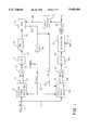
- FIG. 1showing a preferred embodiment of the present invention bit synchronizer 10.
- Hard limited data on line 11is shown being applied to the input of a digital phase detector 12 which is provided with a negative output 13 and a positive output 14.
- the outputs of the digital phase detectorare applied to the input of summing circuit 15 having an output on line 16 applied to the input of a low pass filter 17.
- the filtered output on line 18is applied to the input of a loop filter 19.
- the output of the loop filter on line 21is a phase error voltage which is applied to the input of a voltage controlled oscillator 22.
- the output of the voltage controlled oscillator on line 23is first applied to a divide by 2 circuit 24 which produces at its output the data rate clock on line 25 which is applied to the digital phase detector 12 and to a digital lock detector 26.
- the digital lock detector 26also has a twice or double data rate clock applied thereto on line 23 from the output of the VCO 22.
- the output of the digital lock detector 26is shown having a negative output on line 27 and a positive output on line 28 applied to the input of a summing circuit 29.
- the output of the summing circuit 29 on line 31is applied to the input of a low pass filter 32 shown having a filtered output on line 33.
- the filtered signal on line 33is applied to a comparator 34 having a reference voltage input 35 for comparison purposes.
- the output of the comparator 34 on line 36is a signal indicative of the locked or unlocked condition.
- the signal on line 36is also applied to a sweep circuit 37 shown having an output on line 38 coupled back to the voltage controlled oscillator 22.
- the lock indication signals on line 36may be used to disable the sweep circuit when resolving frequency uncertainties in the input data and/or correcting for the aging of the voltage controlled oscillator crystal.
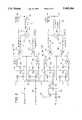
- FIG. 2showing a novel digital implementation of the phase and lock detectors 12 and 26 shown in FIG. 1.
- the hard limited data on line 11is shown being applied to a data input of a D type flip-flop 39 and to a first input of an exclusive OR circuit 41.
- the hard limited data on line 11is similarly applied to the data input of flip-flops 42 through 44 and to a first input of exclusive OR circuits 45 through 47.
- Flip-flop 39is shown having a Q A output on line 48.
- the flip-flops 42 through 44are shown having the Q B through Q D outputs on lines 49 through 51 applied to the second input of the exclusive OR gates 45 through 47.
- the 2R clock on line 23is shown being applied as an inverted signal to the clock input of flip-flop 52 which has a data rate clock on line 25 applied to its data input.
- the flip-flop 52produces a delayed clock on line 53 which is 90° delayed and offset from the data rate clock on line 25.
- the delayed clock on line 53is applied as a negative input to the flip-flop 43 and is also applied as a clock input to the flip-flop 44.
- the delayed clock on line 53is further applied as a positive input and a negative input to OR gates 54 and 55, respectively.
- OR gate 46 on line 56 and the output of exclusive OR gate 47 on line 57are shown being applied as the second inputs to OR gates 54 and 55.
- OR gate 54 on line 27is shown as a composite signal comprising Q c exclusive ORed with the data and this signal is ORed with the delayed clock on line 53.
- OR gate 55 on line 28is shown as a composite signal comprising Q b exclusive ORed with the data and this signal is ORed with the inverted delayed clock on line 53.
- OR gates 54 and 55are applied as negative and positive inputs to the summing circuit 29 which has an output 31 as explained hereinbefore.
- the sum signal on line 31is applied to the low pass filter 32 which produces a filtered output signal on line 33 which is offset 90° from the signal on line 18 and is also shown on FIG. 1 being applied to the comparator 34.
- the output of exclusive OR gate 41 on line 58is shown being applied to OR gate 59 to produce the aforementioned signal on line 13.
- the composite signal on line 13comprises the Q A output exclusive ORed with the data and this composite signal is ORed with the data clock as an input to the negative input of the summing circuit 15.
- the output of OR gate 45 on line 61is applied as an input to the OR gate 62 to produce a composite signal on line 14 which is applied to the positive input of summing circuit 15.
- the composite signal on line 14comprises the output Q B exclusive ORed with the data and this composite signal is ORed with the inverted data rate clock.
- the output of the summing circuit on line 16is applied to the low pass filter 17, having an output 18 which is applied to the loop filter 19 as shown and described in FIG. 1.
- FIG. 3showing a phase S curve, wherein the value of the phase offset in degrees is plotted versus the mean phase error in volts.
- the wave form shown in FIG. 3is being produced as an output signal on line 18.
- This signalcomprises a negative voltage portion 63 of the wave form which results from the rising edge of the clock on line 25 occurring before the zero crossover point of the hard limited data on line 11, thus producing the negative wave form shown as wave form 63 which results in slowing the rate of the voltage control oscillator 22.
- the positive portion of the wave form 64 shown in FIG. 3results from the rising edge of the clock on line 25 occurring after the zero crossover of the hard limited data on line 11, thus, generating a positive output which is applied to the VCO 22 to increase the speed of the VCO.
- FIGS. 1 through 3the portion of FIG. 2 numbered 15 through 18 and 29 through 33 are not part of the digital phase detector and digital lock detector respectively but are analog devices that are compatible with the digital portion shown in FIG. 2. It is a feature of the present invention that the digital portion of FIG. 2 may easily be implemented on a gate array or even a programmable gate array logic chip so as to miniaturize the portion of the bit synchronizer which formally required large components that occupied a large real estate on a printed circuit board. Gate arrays of the type which will accommodate the design shown in FIG. 2 are priced at several dollars and do not require a custom foundry designed chip.
- the digital lock detectorhas a desirable feature in that the output signal on line 36 may be applied to a sweep circuit 37 which is coupled to the VCO 22 by line 38.
- This featureenables the bit synchronizer to be adjusted for aging of the crystal in the voltage controlled oscillator or to permit rapid resolution of the frequency uncertainty in the input data should it be required.
- the bit synchronizeris placed in a vehicle or satellite, the feature of being able to remotely correct for aging or data frequency uncertainty is highly desirable in that the bit synchronizer does not have to be removed from its environmental conditions to make these adjustments.
- phase offset and phase error signalWith respect to FIG. 3, it will be understood that this signal is being produced at the output of the low pass filter 17 on line 18 and the negative portion of the wave form 63 will slow down the voltage control oscillator 22 and the positive portion 64 of the wave form will increase the speed of the oscillator 22, thus adjusting the digital phase detector loop so that the loop attempts to adjust the voltage control oscillator to a phase offset of zero.
- the digital lock detectorwhich has a delayed clock on line 53, causes the signal on line 35 to appear at point 66 of the wave form 64.
- the reference voltage shown on line 35when set at 0.25 volts generates the lock indication signal on line 36 as shown in FIG. 1.
Landscapes
- Engineering & Computer Science (AREA)
- Computer Networks & Wireless Communication (AREA)
- Signal Processing (AREA)
- Stabilization Of Oscillater, Synchronisation, Frequency Synthesizers (AREA)
Abstract
Description
Claims (6)
Priority Applications (1)
| Application Number | Priority Date | Filing Date | Title |
|---|---|---|---|
| US08/171,059US5485484A (en) | 1993-12-21 | 1993-12-21 | Digitally implemented phase and lock indicators for a bit synchronizer |
Applications Claiming Priority (1)
| Application Number | Priority Date | Filing Date | Title |
|---|---|---|---|
| US08/171,059US5485484A (en) | 1993-12-21 | 1993-12-21 | Digitally implemented phase and lock indicators for a bit synchronizer |
Publications (1)
| Publication Number | Publication Date |
|---|---|
| US5485484Atrue US5485484A (en) | 1996-01-16 |
Family
ID=22622334
Family Applications (1)
| Application Number | Title | Priority Date | Filing Date |
|---|---|---|---|
| US08/171,059Expired - LifetimeUS5485484A (en) | 1993-12-21 | 1993-12-21 | Digitally implemented phase and lock indicators for a bit synchronizer |
Country Status (1)
| Country | Link |
|---|---|
| US (1) | US5485484A (en) |
Cited By (20)
| Publication number | Priority date | Publication date | Assignee | Title |
|---|---|---|---|---|
| US5590157A (en)* | 1993-05-19 | 1996-12-31 | U.S. Philips Corporation | Data terminal comprising a demodulator for a FSK phase-coherent modulated signal |
| US5670913A (en)* | 1995-03-31 | 1997-09-23 | Alcatel N.V. | Phase locked loop circuit with false locking detector and a lock acquisition sweep |
| WO1997044893A1 (en)* | 1996-05-20 | 1997-11-27 | Motorola Inc. | Method and apparatus for controlling a phase lock loop |
| US5719908A (en)* | 1995-07-19 | 1998-02-17 | Unisys Corporation | Digital/analog bit synchronizer |
| US5818365A (en)* | 1995-01-13 | 1998-10-06 | Micron Display Technology, Inc. | Serial to parallel conversion with phase locked loop |
| US5903605A (en)* | 1995-03-30 | 1999-05-11 | Intel Corporation | Jitter detection method and apparatus |
| US5909201A (en)* | 1995-01-13 | 1999-06-01 | Micron Technology, Inc. | Timing control for a matrixed scanned array |
| US6052034A (en)* | 1998-06-24 | 2000-04-18 | Industrial Technology Research Institute | Method and apparatus for all digital holdover circuit |
| WO2000031873A1 (en)* | 1998-11-25 | 2000-06-02 | Koninklijke Philips Electronics N.V. | A pulse edge detector with double resolution |
| US6301318B1 (en)* | 1998-03-30 | 2001-10-09 | Pmc-Sierra Ltd. | Pipelined phase detector for clock recovery |
| US20010031028A1 (en)* | 2000-03-07 | 2001-10-18 | Vaucher Cicero Silveira | Data clocked recovery circuit |
| US6560306B1 (en)* | 1997-06-19 | 2003-05-06 | Cypress Semiconductor Corp. | Phase locked loop (PLL) with linear parallel sampling phase detector |
| US6606364B1 (en) | 1999-03-04 | 2003-08-12 | Harris Corporation | Multiple data rate bit synchronizer having phase/frequency detector gain constant proportional to PLL clock divider ratio |
| US6704382B1 (en)* | 1997-07-11 | 2004-03-09 | Tellabs Operations, Inc. | Self-sweeping autolock PLL |
| US6798858B1 (en)* | 2000-02-04 | 2004-09-28 | International Business Machines Corporation | Lock detector for delay or phase locked loops |
| US20050117681A1 (en)* | 2003-12-01 | 2005-06-02 | Lg Electronics Inc. | Timing recovery apparatus and method |
| US20060290438A1 (en)* | 2004-02-27 | 2006-12-28 | Micron Technology, Inc. | Microstrip line dielectric overlay |
| US20080309376A1 (en)* | 2005-11-16 | 2008-12-18 | Chaosheng Song | Mains Phase Detection Apparatus |
| US20090099559A1 (en)* | 2007-10-05 | 2009-04-16 | The Research Foundation Of The State University Of New York | Coherent imaging fiber based hair removal device |
| US7936854B2 (en) | 2002-11-15 | 2011-05-03 | Cypress Semiconductor Corporation | Method and system of cycle slip framing in a deserializer |
Citations (8)
| Publication number | Priority date | Publication date | Assignee | Title |
|---|---|---|---|---|
| US4419760A (en)* | 1982-01-29 | 1983-12-06 | Motorola Inc. | Augmented phase-locked loop for very wide range acquisition and method therefor |
| US4617520A (en)* | 1984-01-03 | 1986-10-14 | Motorola, Inc. | Digital lock detector for a phase-locked loop |
| US4780893A (en)* | 1987-04-16 | 1988-10-25 | Harris Corporation | Bit synchronizer |
| US4837781A (en)* | 1987-04-07 | 1989-06-06 | Gigabit Logic, Inc. | Phase locked loop clock synchronizer and signal detector |
| US5121071A (en)* | 1991-07-31 | 1992-06-09 | Loral Aerospace Corp. | Lock detector for unbalanced QPSK demodulators |
| US5233636A (en)* | 1990-05-11 | 1993-08-03 | Electronics And Telecommunications Research Institute | Analog and digital phase detector for bit synchronism |
| US5301196A (en)* | 1992-03-16 | 1994-04-05 | International Business Machines Corporation | Half-speed clock recovery and demultiplexer circuit |
| US5313499A (en)* | 1992-04-29 | 1994-05-17 | International Business Machines Corporation | Constant gain phase lock-loop |
- 1993
- 1993-12-21USUS08/171,059patent/US5485484A/ennot_activeExpired - Lifetime
Patent Citations (8)
| Publication number | Priority date | Publication date | Assignee | Title |
|---|---|---|---|---|
| US4419760A (en)* | 1982-01-29 | 1983-12-06 | Motorola Inc. | Augmented phase-locked loop for very wide range acquisition and method therefor |
| US4617520A (en)* | 1984-01-03 | 1986-10-14 | Motorola, Inc. | Digital lock detector for a phase-locked loop |
| US4837781A (en)* | 1987-04-07 | 1989-06-06 | Gigabit Logic, Inc. | Phase locked loop clock synchronizer and signal detector |
| US4780893A (en)* | 1987-04-16 | 1988-10-25 | Harris Corporation | Bit synchronizer |
| US5233636A (en)* | 1990-05-11 | 1993-08-03 | Electronics And Telecommunications Research Institute | Analog and digital phase detector for bit synchronism |
| US5121071A (en)* | 1991-07-31 | 1992-06-09 | Loral Aerospace Corp. | Lock detector for unbalanced QPSK demodulators |
| US5301196A (en)* | 1992-03-16 | 1994-04-05 | International Business Machines Corporation | Half-speed clock recovery and demultiplexer circuit |
| US5313499A (en)* | 1992-04-29 | 1994-05-17 | International Business Machines Corporation | Constant gain phase lock-loop |
Cited By (29)
| Publication number | Priority date | Publication date | Assignee | Title |
|---|---|---|---|---|
| US5590157A (en)* | 1993-05-19 | 1996-12-31 | U.S. Philips Corporation | Data terminal comprising a demodulator for a FSK phase-coherent modulated signal |
| US5818365A (en)* | 1995-01-13 | 1998-10-06 | Micron Display Technology, Inc. | Serial to parallel conversion with phase locked loop |
| US5909201A (en)* | 1995-01-13 | 1999-06-01 | Micron Technology, Inc. | Timing control for a matrixed scanned array |
| US5903605A (en)* | 1995-03-30 | 1999-05-11 | Intel Corporation | Jitter detection method and apparatus |
| US5670913A (en)* | 1995-03-31 | 1997-09-23 | Alcatel N.V. | Phase locked loop circuit with false locking detector and a lock acquisition sweep |
| US5719908A (en)* | 1995-07-19 | 1998-02-17 | Unisys Corporation | Digital/analog bit synchronizer |
| WO1997044893A1 (en)* | 1996-05-20 | 1997-11-27 | Motorola Inc. | Method and apparatus for controlling a phase lock loop |
| US5754598A (en)* | 1996-05-23 | 1998-05-19 | Motorola, Inc. | Method and apparatus for controlling a phase lock loop |
| US6560306B1 (en)* | 1997-06-19 | 2003-05-06 | Cypress Semiconductor Corp. | Phase locked loop (PLL) with linear parallel sampling phase detector |
| US6704382B1 (en)* | 1997-07-11 | 2004-03-09 | Tellabs Operations, Inc. | Self-sweeping autolock PLL |
| US6301318B1 (en)* | 1998-03-30 | 2001-10-09 | Pmc-Sierra Ltd. | Pipelined phase detector for clock recovery |
| US6052034A (en)* | 1998-06-24 | 2000-04-18 | Industrial Technology Research Institute | Method and apparatus for all digital holdover circuit |
| WO2000031873A1 (en)* | 1998-11-25 | 2000-06-02 | Koninklijke Philips Electronics N.V. | A pulse edge detector with double resolution |
| US6218869B1 (en)* | 1998-11-25 | 2001-04-17 | Philips Electronics North America Corp. | Pulse detector with double resolution |
| US6606364B1 (en) | 1999-03-04 | 2003-08-12 | Harris Corporation | Multiple data rate bit synchronizer having phase/frequency detector gain constant proportional to PLL clock divider ratio |
| US6798858B1 (en)* | 2000-02-04 | 2004-09-28 | International Business Machines Corporation | Lock detector for delay or phase locked loops |
| US20010031028A1 (en)* | 2000-03-07 | 2001-10-18 | Vaucher Cicero Silveira | Data clocked recovery circuit |
| US7027544B2 (en)* | 2000-03-07 | 2006-04-11 | Koninklijke Philips Electronics N.V. | Data clocked recovery circuit |
| US7936854B2 (en) | 2002-11-15 | 2011-05-03 | Cypress Semiconductor Corporation | Method and system of cycle slip framing in a deserializer |
| US20050117681A1 (en)* | 2003-12-01 | 2005-06-02 | Lg Electronics Inc. | Timing recovery apparatus and method |
| US7440528B2 (en)* | 2003-12-01 | 2008-10-21 | Lg Electronics Inc. | Timing recovery apparatus and method |
| US7436267B2 (en) | 2004-02-27 | 2008-10-14 | Micron Technology, Inc. | Microstrip line dielectric overlay |
| US7432774B2 (en) | 2004-02-27 | 2008-10-07 | Micron Technology, Inc. | Microstrip line dielectric overlay |
| US20090025204A1 (en)* | 2004-02-27 | 2009-01-29 | Micron Technology, Inc. | Microstrip line dielectric overlay |
| US20060290438A1 (en)* | 2004-02-27 | 2006-12-28 | Micron Technology, Inc. | Microstrip line dielectric overlay |
| US9214713B2 (en) | 2004-02-27 | 2015-12-15 | Micron Technology, Inc. | Method of fabricating a microstrip line dielectric overlay |
| US20080309376A1 (en)* | 2005-11-16 | 2008-12-18 | Chaosheng Song | Mains Phase Detection Apparatus |
| US7646225B2 (en)* | 2005-11-16 | 2010-01-12 | Miartech, Inc. | Mains phase detection apparatus |
| US20090099559A1 (en)* | 2007-10-05 | 2009-04-16 | The Research Foundation Of The State University Of New York | Coherent imaging fiber based hair removal device |
Similar Documents
| Publication | Publication Date | Title |
|---|---|---|
| US5485484A (en) | Digitally implemented phase and lock indicators for a bit synchronizer | |
| US4464771A (en) | Phase-locked loop circuit arrangement | |
| US5815016A (en) | Phase-locked delay loop for clock correction | |
| US5712580A (en) | Linear phase detector for half-speed quadrature clocking architecture | |
| US5194828A (en) | Double PLL device | |
| US5400370A (en) | All digital high speed algorithmic data recovery method and apparatus using locally generated compensated broad band time rulers and data edge position averaging | |
| US5018170A (en) | Variable data rate clock synthesizer | |
| JPS61163745A (en) | Phase correlator | |
| WO1980000901A1 (en) | A method of and an arrangement for regulating the phase position of a controlled signal in relation to a reference signal in a telecommunication system | |
| US4072905A (en) | Wide acquisition range MSK demodulator input circuit | |
| WO2001069786A3 (en) | A phase detector | |
| US4639680A (en) | Digital phase and frequency detector | |
| EP0378982B1 (en) | Method and apparatus for automatic phase adjustment in a phase locked loop | |
| CA2138106A1 (en) | CMOS Technology High Speed Digital Signal Transceiver | |
| US5122761A (en) | Digital pll including controllable delay circuit | |
| Sancho | Receiver ASIC for timing, trigger and control distribution in LHC experiments | |
| US5115208A (en) | Pll clock signal regenerator using a phase correlator | |
| CA2196998C (en) | Integrable clock obtaining circuit | |
| US5745314A (en) | Clock generating circuit by using the phase difference between a burst signal and the oscillation signal | |
| US4573024A (en) | PLL having two-frequency VCO | |
| US3449691A (en) | Digital phase-locked loop | |
| US6218907B1 (en) | Frequency comparator and PLL circuit using the same | |
| US4855735A (en) | Recovery of data clock signals | |
| US4891824A (en) | Muting control circuit | |
| KR100389845B1 (en) | Device to synchronize digital receiver |
Legal Events
| Date | Code | Title | Description |
|---|---|---|---|
| AS | Assignment | Owner name:UNISYS CORPORATION Free format text:ASSIGNMENT OF ASSIGNORS INTEREST;ASSIGNORS:WILLIAMS, BRUCE HOWARD;ARBANAS, GLENN ARTHUR;GREEFF, ROY EDGAR;REEL/FRAME:007404/0060 Effective date:19931202 | |
| STCF | Information on status: patent grant | Free format text:PATENTED CASE | |
| FPAY | Fee payment | Year of fee payment:4 | |
| AS | Assignment | Owner name:GOODRICH CORPORATION, NORTH CAROLINA Free format text:ASSIGNMENT OF ASSIGNORS INTEREST;ASSIGNOR:KELSEY-HAYES COMPANY;REEL/FRAME:014015/0523 Effective date:20021001 | |
| FPAY | Fee payment | Year of fee payment:8 | |
| FPAY | Fee payment | Year of fee payment:12 | |
| AS | Assignment | Owner name:UNISYS CORPORATION, PENNSYLVANIA Free format text:RELEASE BY SECURED PARTY;ASSIGNOR:CITIBANK, N.A.;REEL/FRAME:023312/0044 Effective date:20090601 Owner name:UNISYS HOLDING CORPORATION, DELAWARE Free format text:RELEASE BY SECURED PARTY;ASSIGNOR:CITIBANK, N.A.;REEL/FRAME:023312/0044 Effective date:20090601 Owner name:UNISYS CORPORATION,PENNSYLVANIA Free format text:RELEASE BY SECURED PARTY;ASSIGNOR:CITIBANK, N.A.;REEL/FRAME:023312/0044 Effective date:20090601 Owner name:UNISYS HOLDING CORPORATION,DELAWARE Free format text:RELEASE BY SECURED PARTY;ASSIGNOR:CITIBANK, N.A.;REEL/FRAME:023312/0044 Effective date:20090601 | |
| AS | Assignment | Owner name:UNISYS CORPORATION, PENNSYLVANIA Free format text:RELEASE BY SECURED PARTY;ASSIGNOR:CITIBANK, N.A.;REEL/FRAME:023263/0631 Effective date:20090601 Owner name:UNISYS HOLDING CORPORATION, DELAWARE Free format text:RELEASE BY SECURED PARTY;ASSIGNOR:CITIBANK, N.A.;REEL/FRAME:023263/0631 Effective date:20090601 Owner name:UNISYS CORPORATION,PENNSYLVANIA Free format text:RELEASE BY SECURED PARTY;ASSIGNOR:CITIBANK, N.A.;REEL/FRAME:023263/0631 Effective date:20090601 Owner name:UNISYS HOLDING CORPORATION,DELAWARE Free format text:RELEASE BY SECURED PARTY;ASSIGNOR:CITIBANK, N.A.;REEL/FRAME:023263/0631 Effective date:20090601 | |
| AS | Assignment | Owner name:DEUTSCHE BANK TRUST COMPANY AMERICAS, AS COLLATERA Free format text:PATENT SECURITY AGREEMENT (PRIORITY LIEN);ASSIGNOR:UNISYS CORPORATION;REEL/FRAME:023355/0001 Effective date:20090731 | |
| AS | Assignment | Owner name:DEUTSCHE BANK TRUST COMPANY AMERICAS, AS COLLATERA Free format text:PATENT SECURITY AGREEMENT (JUNIOR LIEN);ASSIGNOR:UNISYS CORPORATION;REEL/FRAME:023364/0098 Effective date:20090731 | |
| AS | Assignment | Owner name:GENERAL ELECTRIC CAPITAL CORPORATION, AS AGENT, IL Free format text:SECURITY AGREEMENT;ASSIGNOR:UNISYS CORPORATION;REEL/FRAME:026509/0001 Effective date:20110623 | |
| AS | Assignment | Owner name:UNISYS CORPORATION, PENNSYLVANIA Free format text:RELEASE BY SECURED PARTY;ASSIGNOR:DEUTSCHE BANK TRUST COMPANY;REEL/FRAME:030004/0619 Effective date:20121127 | |
| AS | Assignment | Owner name:UNISYS CORPORATION, PENNSYLVANIA Free format text:RELEASE BY SECURED PARTY;ASSIGNOR:DEUTSCHE BANK TRUST COMPANY AMERICAS, AS COLLATERAL TRUSTEE;REEL/FRAME:030082/0545 Effective date:20121127 | |
| AS | Assignment | Owner name:UNISYS CORPORATION, PENNSYLVANIA Free format text:RELEASE BY SECURED PARTY;ASSIGNOR:WELLS FARGO BANK, NATIONAL ASSOCIATION (SUCCESSOR TO GENERAL ELECTRIC CAPITAL CORPORATION);REEL/FRAME:044416/0358 Effective date:20171005 |