US5483822A - Cantilever and method of using same to detect features on a surface - Google Patents
Cantilever and method of using same to detect features on a surfaceDownload PDFInfo
- Publication number
- US5483822A US5483822AUS08/238,546US23854694AUS5483822AUS 5483822 AUS5483822 AUS 5483822AUS 23854694 AUS23854694 AUS 23854694AUS 5483822 AUS5483822 AUS 5483822A
- Authority
- US
- United States
- Prior art keywords
- cantilever
- cantilever arm
- sample
- tip
- resistance
- Prior art date
- Legal status (The legal status is an assumption and is not a legal conclusion. Google has not performed a legal analysis and makes no representation as to the accuracy of the status listed.)
- Expired - Lifetime
Links
- 238000000034methodMethods0.000titleclaimsdescription19
- 239000004065semiconductorSubstances0.000claimsabstractdescription13
- 229910052710siliconInorganic materials0.000claimsdescription26
- 239000010703siliconSubstances0.000claimsdescription26
- 239000000463materialSubstances0.000claimsdescription6
- 239000000758substrateSubstances0.000abstractdescription17
- 229910052751metalInorganic materials0.000abstractdescription11
- 239000002184metalSubstances0.000abstractdescription11
- 238000005259measurementMethods0.000abstractdescription9
- XUIMIQQOPSSXEZ-UHFFFAOYSA-NSiliconChemical compound[Si]XUIMIQQOPSSXEZ-UHFFFAOYSA-N0.000description25
- 239000000523sampleSubstances0.000description15
- 229920002120photoresistant polymerPolymers0.000description11
- 230000035945sensitivityEffects0.000description8
- 239000007943implantSubstances0.000description7
- 238000004519manufacturing processMethods0.000description7
- 229910052796boronInorganic materials0.000description6
- 239000012212insulatorSubstances0.000description6
- 230000008569processEffects0.000description6
- ZOXJGFHDIHLPTG-UHFFFAOYSA-NBoronChemical compound[B]ZOXJGFHDIHLPTG-UHFFFAOYSA-N0.000description5
- 150000004767nitridesChemical class0.000description5
- 238000000206photolithographyMethods0.000description5
- VYPSYNLAJGMNEJ-UHFFFAOYSA-NSilicium dioxideChemical compoundO=[Si]=OVYPSYNLAJGMNEJ-UHFFFAOYSA-N0.000description4
- 230000003287optical effectEffects0.000description4
- 230000001681protective effectEffects0.000description4
- 229910052814silicon oxideInorganic materials0.000description4
- 239000004642PolyimideSubstances0.000description3
- 229910052785arsenicInorganic materials0.000description3
- RQNWIZPPADIBDY-UHFFFAOYSA-Narsenic atomChemical compound[As]RQNWIZPPADIBDY-UHFFFAOYSA-N0.000description3
- 239000013078crystalSubstances0.000description3
- 238000010586diagramMethods0.000description3
- 238000005530etchingMethods0.000description3
- 238000003384imaging methodMethods0.000description3
- 229920001721polyimidePolymers0.000description3
- 238000004630atomic force microscopyMethods0.000description2
- 230000008901benefitEffects0.000description2
- 230000008859changeEffects0.000description2
- 238000006073displacement reactionMethods0.000description2
- 239000007858starting materialSubstances0.000description2
- 238000012876topographyMethods0.000description2
- -1Boron ionsChemical class0.000description1
- OAICVXFJPJFONN-UHFFFAOYSA-NPhosphorusChemical compound[P]OAICVXFJPJFONN-UHFFFAOYSA-N0.000description1
- 229910052581Si3N4Inorganic materials0.000description1
- 238000005411Van der Waals forceMethods0.000description1
- 229910052782aluminiumInorganic materials0.000description1
- XAGFODPZIPBFFR-UHFFFAOYSA-NaluminiumChemical compound[Al]XAGFODPZIPBFFR-UHFFFAOYSA-N0.000description1
- 238000000137annealingMethods0.000description1
- 238000013459approachMethods0.000description1
- 239000000969carrierSubstances0.000description1
- 238000007796conventional methodMethods0.000description1
- 238000013461designMethods0.000description1
- 239000002019doping agentSubstances0.000description1
- 230000000694effectsEffects0.000description1
- 238000005305interferometryMethods0.000description1
- 238000001459lithographyMethods0.000description1
- 238000012986modificationMethods0.000description1
- 230000004048modificationEffects0.000description1
- 229910052698phosphorusInorganic materials0.000description1
- 239000011574phosphorusSubstances0.000description1
- 238000012545processingMethods0.000description1
- 230000008439repair processEffects0.000description1
- HQVNEWCFYHHQES-UHFFFAOYSA-Nsilicon nitrideChemical compoundN12[Si]34N5[Si]62N3[Si]51N64HQVNEWCFYHHQES-UHFFFAOYSA-N0.000description1
- 230000005641tunnelingEffects0.000description1
- 238000001039wet etchingMethods0.000description1
Images


Classifications
- G—PHYSICS
- G01—MEASURING; TESTING
- G01B—MEASURING LENGTH, THICKNESS OR SIMILAR LINEAR DIMENSIONS; MEASURING ANGLES; MEASURING AREAS; MEASURING IRREGULARITIES OF SURFACES OR CONTOURS
- G01B7/00—Measuring arrangements characterised by the use of electric or magnetic techniques
- G01B7/34—Measuring arrangements characterised by the use of electric or magnetic techniques for measuring roughness or irregularity of surfaces
- G—PHYSICS
- G01—MEASURING; TESTING
- G01Q—SCANNING-PROBE TECHNIQUES OR APPARATUS; APPLICATIONS OF SCANNING-PROBE TECHNIQUES, e.g. SCANNING PROBE MICROSCOPY [SPM]
- G01Q60/00—Particular types of SPM [Scanning Probe Microscopy] or microscopes; Essential components thereof
- G01Q60/24—AFM [Atomic Force Microscopy] or apparatus therefor, e.g. AFM probes
- G01Q60/38—Probes, their manufacture, or their related instrumentation, e.g. holders
- G—PHYSICS
- G01—MEASURING; TESTING
- G01Q—SCANNING-PROBE TECHNIQUES OR APPARATUS; APPLICATIONS OF SCANNING-PROBE TECHNIQUES, e.g. SCANNING PROBE MICROSCOPY [SPM]
- G01Q20/00—Monitoring the movement or position of the probe
- G01Q20/04—Self-detecting probes, i.e. wherein the probe itself generates a signal representative of its position, e.g. piezoelectric gauge
- Y—GENERAL TAGGING OF NEW TECHNOLOGICAL DEVELOPMENTS; GENERAL TAGGING OF CROSS-SECTIONAL TECHNOLOGIES SPANNING OVER SEVERAL SECTIONS OF THE IPC; TECHNICAL SUBJECTS COVERED BY FORMER USPC CROSS-REFERENCE ART COLLECTIONS [XRACs] AND DIGESTS
- Y10—TECHNICAL SUBJECTS COVERED BY FORMER USPC
- Y10S—TECHNICAL SUBJECTS COVERED BY FORMER USPC CROSS-REFERENCE ART COLLECTIONS [XRACs] AND DIGESTS
- Y10S977/00—Nanotechnology
- Y10S977/84—Manufacture, treatment, or detection of nanostructure
- Y10S977/849—Manufacture, treatment, or detection of nanostructure with scanning probe
- Y10S977/85—Scanning probe control process
- Y10S977/851—Particular movement or positioning of scanning tip
- Y—GENERAL TAGGING OF NEW TECHNOLOGICAL DEVELOPMENTS; GENERAL TAGGING OF CROSS-SECTIONAL TECHNOLOGIES SPANNING OVER SEVERAL SECTIONS OF THE IPC; TECHNICAL SUBJECTS COVERED BY FORMER USPC CROSS-REFERENCE ART COLLECTIONS [XRACs] AND DIGESTS
- Y10—TECHNICAL SUBJECTS COVERED BY FORMER USPC
- Y10S—TECHNICAL SUBJECTS COVERED BY FORMER USPC CROSS-REFERENCE ART COLLECTIONS [XRACs] AND DIGESTS
- Y10S977/00—Nanotechnology
- Y10S977/84—Manufacture, treatment, or detection of nanostructure
- Y10S977/849—Manufacture, treatment, or detection of nanostructure with scanning probe
- Y10S977/86—Scanning probe structure
- Y10S977/873—Tip holder
Definitions
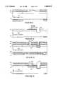
- FIG. 2is a block diagram of a piezoresistor and a resistance measurement circuit.
- FIGS. 7 and 8depict the layout and cross-section of a second preferred embodiment of a microminiature piezoresistive cantilever.
- This second embodiment of the inventionis formed using a silicon-on-insulator (SOl) substrate 200.
- SOlsilicon-on-insulator
Landscapes
- Physics & Mathematics (AREA)
- General Physics & Mathematics (AREA)
- Health & Medical Sciences (AREA)
- General Health & Medical Sciences (AREA)
- Nuclear Medicine, Radiotherapy & Molecular Imaging (AREA)
- Radiology & Medical Imaging (AREA)
- Length Measuring Devices With Unspecified Measuring Means (AREA)
- Measurement Of Length, Angles, Or The Like Using Electric Or Magnetic Means (AREA)
Abstract
Description
TABLE 1 ______________________________________ Longitudinal Coefficient Longitudinal Direction π.sub.L n type π.sub.L p type ______________________________________ 100 π.sub.11 0 111 0 2/3π.sub.44 110 1/4π.sub.11 1/2π.sub.44 112 1/4π.sub.11 1/2π.sub.44 ______________________________________
Vn=(4k.sub.B TR.sub.0 Δf).sup.0.5
Claims (7)
Priority Applications (1)
| Application Number | Priority Date | Filing Date | Title |
|---|---|---|---|
| US08/238,546US5483822A (en) | 1991-01-04 | 1994-05-05 | Cantilever and method of using same to detect features on a surface |
Applications Claiming Priority (3)
| Application Number | Priority Date | Filing Date | Title |
|---|---|---|---|
| US63816391A | 1991-01-04 | 1991-01-04 | |
| US07/954,695US5345815A (en) | 1991-01-04 | 1992-09-30 | Atomic force microscope having cantilever with piezoresistive deflection sensor |
| US08/238,546US5483822A (en) | 1991-01-04 | 1994-05-05 | Cantilever and method of using same to detect features on a surface |
Related Parent Applications (1)
| Application Number | Title | Priority Date | Filing Date |
|---|---|---|---|
| US07/954,695ContinuationUS5345815A (en) | 1991-01-04 | 1992-09-30 | Atomic force microscope having cantilever with piezoresistive deflection sensor |
Publications (1)
| Publication Number | Publication Date |
|---|---|
| US5483822Atrue US5483822A (en) | 1996-01-16 |
Family
ID=24558893
Family Applications (3)
| Application Number | Title | Priority Date | Filing Date |
|---|---|---|---|
| US07/954,695Expired - LifetimeUS5345815A (en) | 1991-01-04 | 1992-09-30 | Atomic force microscope having cantilever with piezoresistive deflection sensor |
| US08/238,546Expired - LifetimeUS5483822A (en) | 1991-01-04 | 1994-05-05 | Cantilever and method of using same to detect features on a surface |
| US08/417,485Expired - LifetimeUS5595942A (en) | 1991-01-04 | 1995-04-05 | Method of fabricating cantilever for atomic force microscope having piezoresistive deflection detector |
Family Applications Before (1)
| Application Number | Title | Priority Date | Filing Date |
|---|---|---|---|
| US07/954,695Expired - LifetimeUS5345815A (en) | 1991-01-04 | 1992-09-30 | Atomic force microscope having cantilever with piezoresistive deflection sensor |
Family Applications After (1)
| Application Number | Title | Priority Date | Filing Date |
|---|---|---|---|
| US08/417,485Expired - LifetimeUS5595942A (en) | 1991-01-04 | 1995-04-05 | Method of fabricating cantilever for atomic force microscope having piezoresistive deflection detector |
Country Status (8)
| Country | Link |
|---|---|
| US (3) | US5345815A (en) |
| EP (1) | EP0619872B1 (en) |
| JP (1) | JPH05196458A (en) |
| KR (1) | KR100214152B1 (en) |
| AU (1) | AU1249692A (en) |
| DE (1) | DE69125956T2 (en) |
| HK (1) | HK1007794A1 (en) |
| WO (1) | WO1992012398A1 (en) |
Cited By (22)
| Publication number | Priority date | Publication date | Assignee | Title |
|---|---|---|---|---|
| US5959200A (en)* | 1997-08-27 | 1999-09-28 | The Board Of Trustees Of The Leland Stanford Junior University | Micromachined cantilever structure providing for independent multidimensional force sensing using high aspect ratio beams |
| US6237399B1 (en) | 1998-01-16 | 2001-05-29 | Bellave S. Shivaram | Cantilever having sensor system for independent measurement of force and torque |
| US6328794B1 (en)* | 1993-06-26 | 2001-12-11 | International Business Machines Corporation | Method of controlling stress in a film |
| US6422069B1 (en)* | 1999-03-16 | 2002-07-23 | Seiko Instruments Inc. | Self-exciting and self-detecting probe and scanning probe apparatus |
| US6530267B2 (en)* | 2000-01-28 | 2003-03-11 | Carl-Zeiss-Stiftung | Scanning system having a deflectable probe tip |
| WO2003101304A1 (en)* | 2002-06-03 | 2003-12-11 | Arizona Board Of Regents | Embedded piezoelectric microcantilever sensors |
| US20040211243A1 (en)* | 2002-06-03 | 2004-10-28 | Porter Timothy L | Embedded piezoelectric microcantilever sensors |
| US20050164299A1 (en)* | 2003-06-03 | 2005-07-28 | Bay Materials Llc | Phase change sensor |
| US6935167B1 (en) | 2004-03-15 | 2005-08-30 | The Board Of Trustees Of The Leland Stanford Junior University | Harmonic cantilevers and imaging methods for atomic force microscopy |
| US20060005614A1 (en)* | 2004-07-08 | 2006-01-12 | Board Of Trustees Of The Leland Stanford | Torsional harmonic cantilevers for detection of high frequency force components in atomic force microscopy |
| US20070119236A1 (en)* | 2004-12-02 | 2007-05-31 | Porter Timothy L | Embedded piezoelectric microcantilever sensors |
| US20080011044A1 (en)* | 2006-07-17 | 2008-01-17 | Workman Richard K | Force method for Determining the Spring Constant of Scanning Probe Microscope Cantilevers using MEMS Actuators |
| US20090004231A1 (en)* | 2007-06-30 | 2009-01-01 | Popp Shane M | Pharmaceutical dosage forms fabricated with nanomaterials for quality monitoring |
| US20090013770A1 (en)* | 2006-10-05 | 2009-01-15 | Roger Proksch | Material property measurements using multiple frequency atomic force microscopy |
| US20090019948A1 (en)* | 2007-07-18 | 2009-01-22 | Gerd Jager | Device for simultaneous measurement of forces |
| US7584653B2 (en) | 2003-08-11 | 2009-09-08 | Veeco Instruments, Inc. | System for wide frequency dynamic nanomechanical analysis |
| US20090231777A1 (en)* | 2008-03-12 | 2009-09-17 | Raravikar Nachiket R | Nanolithographic method of manufacturing an embedded passive device for a microelectronic application, and microelectronic device containing same |
| US20100043107A1 (en)* | 2006-04-25 | 2010-02-18 | Asylum Research Corporation | Multiple Frequency Atomic Force Microscopy |
| US7680553B2 (en) | 2007-03-08 | 2010-03-16 | Smp Logic Systems Llc | Methods of interfacing nanomaterials for the monitoring and execution of pharmaceutical manufacturing processes |
| US20100175155A1 (en)* | 2009-01-06 | 2010-07-08 | President And Fellows Of Harvard College | Measurement and Mapping of Molecular Stretching and Rupture Forces |
| US20110154546A1 (en)* | 2008-06-16 | 2011-06-23 | Roger Proksch | Thermal measurements using multiple frequency atomic force microscopy |
| US9383388B2 (en) | 2014-04-21 | 2016-07-05 | Oxford Instruments Asylum Research, Inc | Automated atomic force microscope and the operation thereof |
Families Citing this family (116)
| Publication number | Priority date | Publication date | Assignee | Title |
|---|---|---|---|---|
| US5266801A (en)* | 1989-06-05 | 1993-11-30 | Digital Instruments, Inc. | Jumping probe microscope |
| JPH05196458A (en)* | 1991-01-04 | 1993-08-06 | Univ Leland Stanford Jr | Piezoresistive cantilever beam structure for atomic force microscopy |
| WO1993011413A1 (en)* | 1991-11-26 | 1993-06-10 | The Australian National University | Piezoelectric bimorph cantilevers for surface analysis instruments |
| US5291775A (en)* | 1992-03-04 | 1994-03-08 | Topometrix | Scanning force microscope with integrated optics and cantilever mount |
| US5672816A (en)* | 1992-03-13 | 1997-09-30 | Park Scientific Instruments | Large stage system for scanning probe microscopes and other instruments |
| US5412980A (en)* | 1992-08-07 | 1995-05-09 | Digital Instruments, Inc. | Tapping atomic force microscope |
| USRE36488E (en)* | 1992-08-07 | 2000-01-11 | Veeco Instruments Inc. | Tapping atomic force microscope with phase or frequency detection |
| US5444244A (en)* | 1993-06-03 | 1995-08-22 | Park Scientific Instruments Corporation | Piezoresistive cantilever with integral tip for scanning probe microscope |
| US5633455A (en)* | 1993-10-05 | 1997-05-27 | Board Of Trustees Of The Leland Stanford, Jr. University | Method of detecting particles of semiconductor wafers |
| US5450746A (en)* | 1993-10-12 | 1995-09-19 | The University Of North Carolina | Constant force stylus profiling apparatus and method |
| US6184053B1 (en)* | 1993-11-16 | 2001-02-06 | Formfactor, Inc. | Method of making microelectronic spring contact elements |
| US7579269B2 (en)* | 1993-11-16 | 2009-08-25 | Formfactor, Inc. | Microelectronic spring contact elements |
| US6727580B1 (en) | 1993-11-16 | 2004-04-27 | Formfactor, Inc. | Microelectronic spring contact elements |
| US5658698A (en)* | 1994-01-31 | 1997-08-19 | Canon Kabushiki Kaisha | Microstructure, process for manufacturing thereof and devices incorporating the same |
| US5742377A (en)* | 1994-04-12 | 1998-04-21 | The Board Of Trustees Of The Leland Stanford, Jr. University | Cantilever for scanning probe microscope including piezoelectric element and method of using the same |
| US6075585A (en)* | 1994-04-12 | 2000-06-13 | The Board Of Trustees Of The Leland Stanford, Jr. University | Vibrating probe for a scanning probe microscope |
| US6000947A (en)* | 1994-04-12 | 1999-12-14 | The Board Of Trustees Of The Leland Stanford, Jr. | Method of fabricating transistor or other electronic device using scanning probe microscope |
| US5666190A (en)* | 1994-04-12 | 1997-09-09 | The Board Of Trustees Of The Leland Stanford, Jr. University | Method of performing lithography using cantilever array |
| US5618760A (en)* | 1994-04-12 | 1997-04-08 | The Board Of Trustees Of The Leland Stanford, Jr. University | Method of etching a pattern on a substrate using a scanning probe microscope |
| US5517280A (en)* | 1994-04-12 | 1996-05-14 | The Board Of Trustees Of The Leland Stanford, Jr. University | Photolithography system |
| US5883705A (en)* | 1994-04-12 | 1999-03-16 | The Board Of Trustees Of The Leland Stanford, Jr. University | Atomic force microscope for high speed imaging including integral actuator and sensor |
| JPH0862230A (en)* | 1994-08-24 | 1996-03-08 | Olympus Optical Co Ltd | Integration type spm sensor |
| WO1996028837A1 (en)* | 1995-03-10 | 1996-09-19 | Molecular Imaging Corporation | Hybrid control system for scanning probe microscopes |
| US5936237A (en)* | 1995-07-05 | 1999-08-10 | Van Der Weide; Daniel Warren | Combined topography and electromagnetic field scanning probe microscope |
| US5705814A (en)* | 1995-08-30 | 1998-01-06 | Digital Instruments, Inc. | Scanning probe microscope having automatic probe exchange and alignment |
| WO1997009584A1 (en)* | 1995-09-01 | 1997-03-13 | International Business Machines Corporation | Cantilever with integrated deflection sensor |
| US5630932A (en)* | 1995-09-06 | 1997-05-20 | Molecular Imaging Corporation | Tip etching system and method for etching platinum-containing wire |
| US5874668A (en) | 1995-10-24 | 1999-02-23 | Arch Development Corporation | Atomic force microscope for biological specimens |
| US5929643A (en)* | 1995-12-07 | 1999-07-27 | Olympus Optical Co., Ltd. | Scanning probe microscope for measuring the electrical properties of the surface of an electrically conductive sample |
| JP3599880B2 (en)* | 1996-03-12 | 2004-12-08 | オリンパス株式会社 | Cantilever tip |
| EP0802394B1 (en)* | 1996-04-18 | 2003-06-11 | Seiko Instruments Inc. | Semiconductor distortion sensors with pn junction, scanning probe microscope |
| US5907095A (en)* | 1996-06-17 | 1999-05-25 | Industrial Technology Research Institute | High-sensitivity strain probe |
| US5856672A (en)* | 1996-08-29 | 1999-01-05 | International Business Machines Corporation | Single-crystal silicon cantilever with integral in-plane tip for use in atomic force microscope system |
| US5729026A (en)* | 1996-08-29 | 1998-03-17 | International Business Machines Corporation | Atomic force microscope system with angled cantilever having integral in-plane tip |
| JP3260644B2 (en)* | 1996-12-10 | 2002-02-25 | セイコーインスツルメンツ株式会社 | Cantilever and manufacturing method thereof |
| US5822285A (en)* | 1997-03-31 | 1998-10-13 | International Business Machines Corporation | Atomic force microscopy disk data storage system with nonradial tracking lines |
| RU2121657C1 (en)* | 1997-05-08 | 1998-11-10 | Зао "Нт-Мдт" | Process of formation of cantilever of scanning probing microscope |
| JPH10312592A (en)* | 1997-05-13 | 1998-11-24 | Canon Inc | Information processing apparatus and information processing method |
| US5804710A (en)* | 1997-06-05 | 1998-09-08 | International Business Machines Corporation | Atomic force microscope system with multi-directional voice coil actuator for controlling the stylus |
| JP3511361B2 (en)* | 1997-08-04 | 2004-03-29 | セイコーインスツルメンツ株式会社 | Scanning probe microscope |
| US5952657A (en)* | 1997-08-22 | 1999-09-14 | Thermo Microscopes, Corp. | Atomic force microscope with integrated optics for attachment to optical microscope |
| AU8760698A (en)* | 1997-08-22 | 1999-03-16 | Park Scientific Instruments | Scanning probe microscope system removably attachable to an optical microscope objective |
| US5856967A (en)* | 1997-08-27 | 1999-01-05 | International Business Machines Corporation | Atomic force microscopy data storage system with tracking servo from lateral force-sensing cantilever |
| DE19740763C2 (en)* | 1997-09-16 | 2001-06-07 | Forschungszentrum Juelich Gmbh | Lever arm for an atomic force microscope |
| JPH11304825A (en)* | 1997-09-30 | 1999-11-05 | Seiko Instruments Inc | Semiconductor distortion sensor and its manufacture, and scanning probe microscope |
| JP3700910B2 (en)* | 1997-10-16 | 2005-09-28 | セイコーインスツル株式会社 | Semiconductor strain sensor, manufacturing method thereof, and scanning probe microscope |
| JP3883699B2 (en) | 1997-11-20 | 2007-02-21 | エスアイアイ・ナノテクノロジー株式会社 | Self-sensing SPM probe and SPM device |
| US6018390A (en)* | 1998-01-27 | 2000-01-25 | Rice Systems, Inc. | Integrated optics waveguide accelerometer with a proof mass adapted to exert force against the optical waveguide during acceleration |
| JP3723681B2 (en)* | 1998-03-11 | 2005-12-07 | 株式会社島津製作所 | Micromaterial testing equipment |
| US6287885B1 (en)* | 1998-05-08 | 2001-09-11 | Denso Corporation | Method for manufacturing semiconductor dynamic quantity sensor |
| US6259089B1 (en) | 1998-05-15 | 2001-07-10 | Rice Systems, Inc. | Integrated optics rotation sensor |
| US6635311B1 (en) | 1999-01-07 | 2003-10-21 | Northwestern University | Methods utilizing scanning probe microscope tips and products therefor or products thereby |
| US6827979B2 (en)* | 1999-01-07 | 2004-12-07 | Northwestern University | Methods utilizing scanning probe microscope tips and products therefor or produced thereby |
| US6330824B1 (en)* | 1999-02-19 | 2001-12-18 | The University Of North Carolina At Chapel Hill | Photothermal modulation for oscillating mode atomic force microscopy in solution |
| JP3387846B2 (en)* | 1999-03-04 | 2003-03-17 | セイコーインスツルメンツ株式会社 | Scanning probe microscope |
| TW408417B (en)* | 1999-05-03 | 2000-10-11 | Ind Tech Res Inst | Planar-shape thin probe having electrostatic actuator manufactured by using sacrificed layer technology and its manufacturing method |
| US6369385B1 (en) | 1999-05-05 | 2002-04-09 | Applied Materials, Inc. | Integrated microcolumn and scanning probe microscope arrays |
| JP3785018B2 (en)* | 2000-03-13 | 2006-06-14 | エスアイアイ・ナノテクノロジー株式会社 | Microprobe and scanning probe apparatus using the same |
| EP1348113B1 (en) | 2000-08-15 | 2008-07-30 | Bioforce Nanosciences, Inc. | Nanoscale molecular arrayer |
| KR100424540B1 (en)* | 2001-04-21 | 2004-03-30 | (주)지우텍 | Cantilever construction composed of multiple actuators for AFM, AFM system having the cantilever construction and measurement method for properties of material by using the AFM |
| US6718821B1 (en) | 2001-11-07 | 2004-04-13 | Sandia Corporation | Laser interferometry force-feedback sensor for an interfacial force microscope |
| US7108992B2 (en)* | 2002-11-27 | 2006-09-19 | St. Jude Children's Research Hospital | ATM kinase compositions and methods |
| EP1588153B1 (en)* | 2002-12-27 | 2007-10-03 | NanoNord A/S | A cantilever sensor using both the longitudinal and the transversal piezoresistive coefficients |
| AU2003243125A1 (en)* | 2003-06-18 | 2005-01-04 | Atilla Aydinli | Integrated optical displacement sensors for scanning probe microscopy |
| US7315505B2 (en)* | 2003-07-14 | 2008-01-01 | Hewlett-Packard Development Company, L.P. | Storage device having a probe with plural tips |
| US7173314B2 (en)* | 2003-08-13 | 2007-02-06 | Hewlett-Packard Development Company, L.P. | Storage device having a probe and a storage cell with moveable parts |
| US7215633B2 (en)* | 2003-08-13 | 2007-05-08 | Hewlett-Packard Development Company, L.P. | Storage device having a probe with a tip to form a groove in a storage medium |
| KR100613398B1 (en)* | 2003-11-25 | 2006-08-17 | 한국과학기술연구원 | Cantilever sensor type analysis system, manufacturing method and ultrafine material detection method using the same |
| US20050128927A1 (en)* | 2003-12-15 | 2005-06-16 | Hewlett-Packard Development Co., L.P. | Electrostatic actuator for contact probe storage device |
| US7423954B2 (en)* | 2003-12-17 | 2008-09-09 | Hewlett-Packard Development Company, L.P. | Contact probe storage sensor pod |
| US7436753B2 (en) | 2003-12-17 | 2008-10-14 | Mejia Robert G | Contact probe storage FET sensor |
| US7212487B2 (en)* | 2004-01-07 | 2007-05-01 | Hewlett-Packard Development Company, L.P. | Data readout arrangement |
| US7164646B2 (en)* | 2004-02-19 | 2007-01-16 | Hewlett-Packard Development Company, L.P. | Storage device having a storage cell programmable to one of more than two storage states |
| US7184388B2 (en)* | 2004-03-09 | 2007-02-27 | Hewlett-Packard Development Company, L.P. | Heating elements for a storage device |
| US7167434B2 (en)* | 2004-03-09 | 2007-01-23 | Hewlett-Packard Development Company, L.P. | Storage device having a probe with a first plate that cooperates with a second plate to provide a variable capacitance |
| US7167435B2 (en)* | 2004-03-09 | 2007-01-23 | Hewlett-Packard Development Company, L.P. | Storage device having a probe with plural tips |
| US7254108B2 (en)* | 2004-03-15 | 2007-08-07 | Hewlett-Packard Development Company, L.P. | Storage device including a probe having an electrically conductive tip portion for electrical contact with a storage medium |
| US6999403B2 (en)* | 2004-04-02 | 2006-02-14 | Hewlett-Packard Development Company, L.P. | Storage device having a probe to cooperate with a storage medium to provide a variable resistance |
| US7009268B2 (en)* | 2004-04-21 | 2006-03-07 | Hewlett-Packard Development Company, L.P. | Wheatstone bridge scheme for sensor |
| US7301886B2 (en)* | 2004-05-10 | 2007-11-27 | Hewlett-Packard Development Company, L.P. | Storage device having a read circuit to detect a storage state based on interaction between a probe and a storage medium |
| US7362549B2 (en)* | 2004-05-19 | 2008-04-22 | Seagate Technology Llc | Storage device having first and second magnetic elements that interact magnetically to indicate a storage state |
| US7310298B2 (en)* | 2004-05-20 | 2007-12-18 | Hewlett-Packard Development Company, L.P. | Storage device having a probe to form structures for representing data states |
| US7236446B2 (en)* | 2004-07-23 | 2007-06-26 | Hewlett-Packard Development Company, L.P. | Compensating for variations in the temperature of a probe of a storage device |
| KR100580652B1 (en)* | 2004-08-27 | 2006-05-16 | 삼성전자주식회사 | Manufacturing method of semiconductor probe with resistive tip |
| US7212488B2 (en) | 2005-03-21 | 2007-05-01 | Hewlett-Packard Development Company, L.P. | Method and device enabling capacitive probe-based data storage readout |
| US7989164B2 (en)* | 2005-04-22 | 2011-08-02 | The Board Of Trustees Of The Leland Stanford Junior University | Detection of macromolecular complexes with harmonic cantilevers |
| US8067169B2 (en)* | 2005-04-22 | 2011-11-29 | The Board Of Trustees Of The Leland Stanford Junior University | Detection of macromolecular complexes on ultraflat surfaces with harmonic cantilevers |
| CN1313357C (en)* | 2005-08-04 | 2007-05-02 | 上海交通大学 | Integration manufacturing method of cantilever beam type dot needle-point based on silicon oxide film |
| US20100294927A1 (en)* | 2005-09-12 | 2010-11-25 | Nanolnk, Inc. | High throughput inspecting |
| KR100771851B1 (en)* | 2006-07-21 | 2007-10-31 | 전자부품연구원 | Atomic Force Microscopy Cantilever with Field Effect Transistor and its Manufacturing Method |
| US7423264B2 (en)* | 2006-09-08 | 2008-09-09 | Kla-Tencor Technologies Corporation | Atomic force microscope |
| EP1953516B1 (en)* | 2007-01-31 | 2011-03-09 | Infineon Technologies AG | Micromechanical pressure sensing device |
| KR100796204B1 (en)* | 2007-02-12 | 2008-01-24 | 주식회사 유니테스트 | Method for manufacturing cantilever structure of probe card |
| US7958776B2 (en)* | 2007-09-06 | 2011-06-14 | Chunhai Wang | Atomic force gradient microscope and method of using this microscope |
| US7928343B2 (en)* | 2007-12-04 | 2011-04-19 | The Board Of Trustees Of The University Of Illinois | Microcantilever heater-thermometer with integrated temperature-compensated strain sensor |
| US7861315B2 (en)* | 2007-12-11 | 2010-12-28 | Asylum Research Corporation | Method for microfabricating a probe with integrated handle, cantilever, tip and circuit |
| CN100573071C (en)* | 2007-12-28 | 2009-12-23 | 中国科学院上海微系统与信息技术研究所 | The pressure drag structure and the detection method of mos capacitance substrate on the nano beam |
| US8719960B2 (en)* | 2008-01-31 | 2014-05-06 | The Board Of Trustees Of The University Of Illinois | Temperature-dependent nanoscale contact potential measurement technique and device |
| JP5046039B2 (en)* | 2008-04-16 | 2012-10-10 | エスアイアイ・ナノテクノロジー株式会社 | Liquid observation sensor and liquid observation device |
| WO2009140440A1 (en)* | 2008-05-13 | 2009-11-19 | Nanoink, Inc. | Dual-tip cantilever |
| US8931950B2 (en) | 2008-08-20 | 2015-01-13 | The Board Of Trustees Of The University Of Illinois | Device for calorimetric measurement |
| US8332961B2 (en)* | 2008-09-22 | 2012-12-11 | International Business Machines Corporation | Platinum silicide tip apices for probe-based technologies |
| BG110397A (en) | 2009-06-05 | 2010-12-30 | Амг Технолоджи Оод | Method for receiving devices for mems with electric elements on their sidewalls |
| US8387443B2 (en)* | 2009-09-11 | 2013-03-05 | The Board Of Trustees Of The University Of Illinois | Microcantilever with reduced second harmonic while in contact with a surface and nano scale infrared spectrometer |
| US8762075B2 (en)* | 2009-09-29 | 2014-06-24 | Lawrence Livermore National Security, Llc | Microcantilever-based gas sensor employing two simultaneous physical sensing modes |
| BG66424B1 (en) | 2009-09-29 | 2014-03-31 | "Амг Технолоджи" Оод | Sensors for scanning probing microscopy, a method of three-dimensional measuing and a method for producing such sensors |
| US8643140B2 (en)* | 2011-07-11 | 2014-02-04 | United Microelectronics Corp. | Suspended beam for use in MEMS device |
| US8914911B2 (en) | 2011-08-15 | 2014-12-16 | The Board Of Trustees Of The University Of Illinois | Magnetic actuation and thermal cantilevers for temperature and frequency dependent atomic force microscopy |
| US8533861B2 (en) | 2011-08-15 | 2013-09-10 | The Board Of Trustees Of The University Of Illinois | Magnetic actuation and thermal cantilevers for temperature and frequency dependent atomic force microscopy |
| US8740209B2 (en)* | 2012-02-22 | 2014-06-03 | Expresslo Llc | Method and apparatus for ex-situ lift-out specimen preparation |
| US9395388B2 (en) | 2012-09-14 | 2016-07-19 | The University Of North Carolina At Chapel Hill | Methods, systems, and computer readable media for dual resonance frequency enhanced electrostatic force microscopy |
| CN103615969B (en)* | 2013-11-22 | 2016-04-06 | 同济大学 | A kind of portable Rock Joint Plane roughness measuring instrument |
| CN104360107B (en)* | 2014-11-12 | 2016-11-30 | 苏州大学 | Graphene-coated atomic force microscope probe and preparation method and application thereof |
| US9625331B2 (en) | 2015-09-10 | 2017-04-18 | International Business Machines Corporation | Surface force apparatus based on a spherical lens |
| CN109870100B (en)* | 2018-12-28 | 2020-12-01 | 西北工业大学 | A device and method for measuring deformation of shock-absorbing block in launch cylinder |
| CN111827246A (en)* | 2020-07-20 | 2020-10-27 | 潍坊润宜科新材料有限公司 | Laying construction method of intelligent machine-sensitive belt |
Citations (8)
| Publication number | Priority date | Publication date | Assignee | Title |
|---|---|---|---|---|
| US4106333A (en)* | 1975-08-12 | 1978-08-15 | Ernst Salje | Method of and apparatus for examining the roughness of surfaces |
| US4166384A (en)* | 1977-09-07 | 1979-09-04 | Hitachi, Ltd. | Semiconductor transducer |
| US4359892A (en)* | 1979-12-15 | 1982-11-23 | U.S. Philips Corporation | Arrangement for measuring surface profiles |
| US4454771A (en)* | 1980-11-07 | 1984-06-19 | Hitachi, Ltd. | Load cell |
| US4706374A (en)* | 1984-10-19 | 1987-11-17 | Nissan Motor Co., Ltd. | Method of manufacture for semiconductor accelerometer |
| EP0387906A2 (en)* | 1989-03-17 | 1990-09-19 | Olympus Optical Co., Ltd. | Sensor having a cantilever |
| US5329808A (en)* | 1989-12-08 | 1994-07-19 | Digital Instruments, Inc. | Atomic force microscope |
| US5345815A (en)* | 1991-01-04 | 1994-09-13 | Board Of Trustees, Leland Stanford Jr. University | Atomic force microscope having cantilever with piezoresistive deflection sensor |
Family Cites Families (29)
| Publication number | Priority date | Publication date | Assignee | Title |
|---|---|---|---|---|
| US2405133A (en)* | 1942-10-07 | 1946-08-06 | Brush Dev Co | Method and means for measuring surface roughness |
| US2460726A (en)* | 1943-01-11 | 1949-02-01 | Brush Dev Co | Surface roughness measuring device |
| US3049002A (en)* | 1959-02-24 | 1962-08-14 | Hediger Hermann | Device for measuring the roughness of surfaces |
| US3378648A (en)* | 1964-12-31 | 1968-04-16 | Gen Electric | Doped piezoresistive phonograph pickup |
| US3893228A (en)* | 1972-10-02 | 1975-07-08 | Motorola Inc | Silicon pressure sensor |
| CA1078217A (en)* | 1976-03-31 | 1980-05-27 | Robert C. Whitehead (Jr.) | Force transducing cantilever beam and pressure transducer incorporating it |
| US4203327A (en)* | 1978-06-29 | 1980-05-20 | Honeywell Inc. | Piezoresistive silicon strain sensors and pressure transducers incorporating them |
| US4498229A (en)* | 1982-10-04 | 1985-02-12 | Becton, Dickinson And Company | Piezoresistive transducer |
| US4522072A (en)* | 1983-04-22 | 1985-06-11 | Insouth Microsystems, Inc. | Electromechanical transducer strain sensor arrangement and construction |
| US4793194A (en)* | 1985-03-26 | 1988-12-27 | Endevco Corporation | Piezoresistive transducer |
| US4737473A (en)* | 1985-03-26 | 1988-04-12 | Endevco Corporation | Piezoresistive transducer |
| USRE33387E (en)* | 1985-11-26 | 1990-10-16 | International Business Machines Corporation | Atomic force microscope and method for imaging surfaces with atomic resolution |
| JPH0750789B2 (en)* | 1986-07-18 | 1995-05-31 | 日産自動車株式会社 | Method for manufacturing semiconductor pressure converter |
| JPS6376483A (en)* | 1986-09-19 | 1988-04-06 | Fujitsu Ltd | Manufacture of semiconductor acceleration sensor |
| SU1504485A1 (en)* | 1988-01-25 | 1989-08-30 | Пермский политехнический институт | Roughness sensor |
| US4906840A (en)* | 1988-01-27 | 1990-03-06 | The Board Of Trustees Of Leland Stanford Jr., University | Integrated scanning tunneling microscope |
| JPH07113647B2 (en)* | 1988-09-02 | 1995-12-06 | 日産自動車株式会社 | Semiconductor acceleration sensor |
| US5221415A (en)* | 1989-01-17 | 1993-06-22 | Board Of Trustees Of The Leland Stanford Junior University | Method of forming microfabricated cantilever stylus with integrated pyramidal tip |
| US4943719A (en)* | 1989-01-17 | 1990-07-24 | The Board Of Trustees Of The Leland Stanford University | Microminiature cantilever stylus |
| FR2643148B1 (en)* | 1989-02-15 | 1991-12-06 | Schlumberger Ind Sa | SEMICONDUCTOR-ON-INSULATION PRESSURE SENSOR |
| US5229606A (en)* | 1989-06-05 | 1993-07-20 | Digital Instruments, Inc. | Jumping probe microscope |
| US5015850A (en)* | 1989-06-20 | 1991-05-14 | The Board Of Trustees Of The Leland Stanford Junior University | Microfabricated microscope assembly |
| US4968585A (en)* | 1989-06-20 | 1990-11-06 | The Board Of Trustees Of The Leland Stanford Jr. University | Microfabricated cantilever stylus with integrated conical tip |
| EP0413042B1 (en)* | 1989-08-16 | 1992-12-16 | International Business Machines Corporation | Method of producing micromechanical sensors for the afm/stm profilometry and micromechanical afm/stm sensor head |
| US5021364A (en)* | 1989-10-31 | 1991-06-04 | The Board Of Trustees Of The Leland Stanford Junior University | Microcantilever with integral self-aligned sharp tetrahedral tip |
| US4993506A (en)* | 1989-12-11 | 1991-02-19 | Shlomo Angel | Mass-produced flat one-piece load cell and scales incorporating it |
| US5210410A (en)* | 1991-09-26 | 1993-05-11 | The Board Of Trustees Of The Leland Stanford Junior University | Scanning probe microscope having scan correction |
| US5386720A (en)* | 1992-01-09 | 1995-02-07 | Olympus Optical Co., Ltd. | Integrated AFM sensor |
| US5444244A (en)* | 1993-06-03 | 1995-08-22 | Park Scientific Instruments Corporation | Piezoresistive cantilever with integral tip for scanning probe microscope |
- 1991
- 1991-12-27JPJP3346134Apatent/JPH05196458A/enactivePending
- 1991-12-30EPEP92904827Apatent/EP0619872B1/ennot_activeExpired - Lifetime
- 1991-12-30AUAU12496/92Apatent/AU1249692A/ennot_activeAbandoned
- 1991-12-30WOPCT/US1991/009759patent/WO1992012398A1/enactiveIP Right Grant
- 1991-12-30KRKR1019930701995Apatent/KR100214152B1/ennot_activeExpired - Fee Related
- 1991-12-30DEDE69125956Tpatent/DE69125956T2/ennot_activeExpired - Fee Related
- 1991-12-30HKHK98107022Apatent/HK1007794A1/ennot_activeIP Right Cessation
- 1992
- 1992-09-30USUS07/954,695patent/US5345815A/ennot_activeExpired - Lifetime
- 1994
- 1994-05-05USUS08/238,546patent/US5483822A/ennot_activeExpired - Lifetime
- 1995
- 1995-04-05USUS08/417,485patent/US5595942A/ennot_activeExpired - Lifetime
Patent Citations (8)
| Publication number | Priority date | Publication date | Assignee | Title |
|---|---|---|---|---|
| US4106333A (en)* | 1975-08-12 | 1978-08-15 | Ernst Salje | Method of and apparatus for examining the roughness of surfaces |
| US4166384A (en)* | 1977-09-07 | 1979-09-04 | Hitachi, Ltd. | Semiconductor transducer |
| US4359892A (en)* | 1979-12-15 | 1982-11-23 | U.S. Philips Corporation | Arrangement for measuring surface profiles |
| US4454771A (en)* | 1980-11-07 | 1984-06-19 | Hitachi, Ltd. | Load cell |
| US4706374A (en)* | 1984-10-19 | 1987-11-17 | Nissan Motor Co., Ltd. | Method of manufacture for semiconductor accelerometer |
| EP0387906A2 (en)* | 1989-03-17 | 1990-09-19 | Olympus Optical Co., Ltd. | Sensor having a cantilever |
| US5329808A (en)* | 1989-12-08 | 1994-07-19 | Digital Instruments, Inc. | Atomic force microscope |
| US5345815A (en)* | 1991-01-04 | 1994-09-13 | Board Of Trustees, Leland Stanford Jr. University | Atomic force microscope having cantilever with piezoresistive deflection sensor |
Non-Patent Citations (10)
| Title |
|---|
| IBM Technical Disclosure Bulletin vol. 10, No. 8, Jan. 1968, New York US p. 1259 R. J. Wilfinger; R. A. Carballo `Speech Coder Utilizing Semiconductor Cantilevers`. |
| IBM Technical Disclosure Bulletin vol. 10, No. 8, Jan. 1968, New York US p. 1259 R. J. Wilfinger; R. A. Carballo Speech Coder Utilizing Semiconductor Cantilevers .* |
| IEEE Electron Device Letters., vol. 10, No. 11, Nov. 1989, New York US pp. 490 492 S. Akamine et al Microfabricated Scanning Tunneling Microscope .* |
| IEEE Electron Device Letters., vol. 10, No. 11, Nov. 1989, New York US pp. 490-492 S. Akamine et al `Microfabricated Scanning Tunneling Microscope`. |
| IEEE Transactions on Electron Devices, vol. ED 26, No. 12, Dec. 1979, New York US pp. 1911 1917 L. M. Roylance; J. B. Angell A Batch Fabricated Silicon Accelerometer .* |
| IEEE Transactions on Electron Devices, vol. ED-26, No. 12, Dec. 1979, New York US pp. 1911-1917 L. M. Roylance; J. B. Angell `A Batch Fabricated Silicon Accelerometer`. |
| Transactions of the Institute of Electrical Engineers of Japan, Part C, vol. 122 C, No. 12, Dec. 1992, Japan Yonekubo et al Contract type line sensor for examining surface topography *abstract; figures* pp. 757 762.* |
| Transactions of the Institute of Electrical Engineers of Japan, Part C, vol. 122-C, No. 12, Dec. 1992, Japan Yonekubo et al "Contract type line sensor for examining surface topography" *abstract; figures* pp. 757-762. |
| Transducers 91.1991 International Conference on Solid State Sensors and Actuators Digest of Technical Papers (cat. No. 91ch2817 5), San Francisco, Calif. USA, 24 27 Jun. 1991. Atomic force microscopy using a peizoresistive cantilever (M. Tortonese et al.), *pp. 448 451.* |
| Transducers '91.1991 International Conference on Solid State Sensors and Actuators Digest of Technical Papers (cat. No. 91ch2817-5), San Francisco, Calif. USA, 24-27 Jun. 1991. "Atomic force microscopy using a peizoresistive cantilever" (M. Tortonese et al.), *pp. 448-451. |
Cited By (51)
| Publication number | Priority date | Publication date | Assignee | Title |
|---|---|---|---|---|
| US6328794B1 (en)* | 1993-06-26 | 2001-12-11 | International Business Machines Corporation | Method of controlling stress in a film |
| US5959200A (en)* | 1997-08-27 | 1999-09-28 | The Board Of Trustees Of The Leland Stanford Junior University | Micromachined cantilever structure providing for independent multidimensional force sensing using high aspect ratio beams |
| US6237399B1 (en) | 1998-01-16 | 2001-05-29 | Bellave S. Shivaram | Cantilever having sensor system for independent measurement of force and torque |
| US6422069B1 (en)* | 1999-03-16 | 2002-07-23 | Seiko Instruments Inc. | Self-exciting and self-detecting probe and scanning probe apparatus |
| US6530267B2 (en)* | 2000-01-28 | 2003-03-11 | Carl-Zeiss-Stiftung | Scanning system having a deflectable probe tip |
| US20040211243A1 (en)* | 2002-06-03 | 2004-10-28 | Porter Timothy L | Embedded piezoelectric microcantilever sensors |
| US7168294B2 (en) | 2002-06-03 | 2007-01-30 | Arizona Board Of Reagents | Embedded piezoelectric microcantilever sensors |
| US6854317B2 (en) | 2002-06-03 | 2005-02-15 | Arizona Board Of Regents Acting For Arizona State University | Embedded piezoelectric microcantilever sensors |
| US20090090168A1 (en)* | 2002-06-03 | 2009-04-09 | Porter Timothy L | Embedded Piezoelectric Microcantilever Sensors |
| CN100473350C (en)* | 2002-06-03 | 2009-04-01 | 北亚利桑那大学董事会 | Embedded piezoelectric microcantilever sensors |
| WO2003101304A1 (en)* | 2002-06-03 | 2003-12-11 | Arizona Board Of Regents | Embedded piezoelectric microcantilever sensors |
| US20060053871A1 (en)* | 2002-06-03 | 2006-03-16 | Porter Timothy L | Embedded piezoelectric microcantilever sensors |
| US7726175B2 (en) | 2002-06-03 | 2010-06-01 | Arizona Board Of Regents, A Body Corporate Of The State Of Arizona, Acting For Northern Arizona University | Embedded piezoelectric microcantilever sensors |
| US20070249059A1 (en)* | 2003-06-03 | 2007-10-25 | Stewart Ray F | Phase change sensor |
| US20050164299A1 (en)* | 2003-06-03 | 2005-07-28 | Bay Materials Llc | Phase change sensor |
| US7794657B2 (en) | 2003-06-03 | 2010-09-14 | Cantimer, Inc. | Phase change sensor |
| US7584653B2 (en) | 2003-08-11 | 2009-09-08 | Veeco Instruments, Inc. | System for wide frequency dynamic nanomechanical analysis |
| US7451638B1 (en) | 2004-03-15 | 2008-11-18 | The Board Of Trustees Of The Leland Stanford Junior University | Harmonic cantilevers and imaging methods for atomic force microscopy |
| US6935167B1 (en) | 2004-03-15 | 2005-08-30 | The Board Of Trustees Of The Leland Stanford Junior University | Harmonic cantilevers and imaging methods for atomic force microscopy |
| US7302833B2 (en) | 2004-07-08 | 2007-12-04 | The Board Of Trustees Of The Leland Stanford Junior University | Torsional harmonic cantilevers for detection of high frequency force components in atomic force microscopy |
| US20080041143A1 (en)* | 2004-07-08 | 2008-02-21 | The Board Of Trustees Of The Leland Stanford Junior University | Atomic Force Microscope Using A Torsional Harmonic Cantilever |
| US7404314B2 (en) | 2004-07-08 | 2008-07-29 | The Board Of Trustees Of The Leland Stanford Junior University | Atomic force microscope using a torsional harmonic cantilever |
| US7089787B2 (en) | 2004-07-08 | 2006-08-15 | Board Of Trustees Of The Leland Stanford Junior University | Torsional harmonic cantilevers for detection of high frequency force components in atomic force microscopy |
| US20060005614A1 (en)* | 2004-07-08 | 2006-01-12 | Board Of Trustees Of The Leland Stanford | Torsional harmonic cantilevers for detection of high frequency force components in atomic force microscopy |
| US20060236757A1 (en)* | 2004-07-08 | 2006-10-26 | The Board Of Trustees Of The Leland Stanford Junior University | Torsional Harmonic Cantilevers For Detection Of High Frequency Force Components In Atomic Force Microscopy |
| US7395693B2 (en) | 2004-12-02 | 2008-07-08 | The Arizona Board of Regents, a body corporate of the state of Arizona acting for Northern Arizona University | Embedded piezoelectric microcantilever sensors |
| US20070119236A1 (en)* | 2004-12-02 | 2007-05-31 | Porter Timothy L | Embedded piezoelectric microcantilever sensors |
| US8448501B2 (en) | 2006-04-25 | 2013-05-28 | Oxford Instruments Plc | Multiple frequency atomic force microscopy |
| US9069007B2 (en) | 2006-04-25 | 2015-06-30 | Oxford Instruments Plc | Multiple frequency atomic force microscopy |
| US20100043107A1 (en)* | 2006-04-25 | 2010-02-18 | Asylum Research Corporation | Multiple Frequency Atomic Force Microscopy |
| US7395697B2 (en)* | 2006-07-17 | 2008-07-08 | Agilent Technologies, Inc. | Force method for determining the spring constant of scanning probe microscope cantilevers using MEMS actuators |
| US20080011044A1 (en)* | 2006-07-17 | 2008-01-17 | Workman Richard K | Force method for Determining the Spring Constant of Scanning Probe Microscope Cantilevers using MEMS Actuators |
| US20090013770A1 (en)* | 2006-10-05 | 2009-01-15 | Roger Proksch | Material property measurements using multiple frequency atomic force microscopy |
| US10215773B2 (en) | 2006-10-05 | 2019-02-26 | Oxford Instruments Afm Inc | Material property measurements using multiple frequency atomic force microscopy |
| US8555711B2 (en) | 2006-10-05 | 2013-10-15 | Asylum Research Corporation | Material property measurements using multiple frequency atomic fore microscopy |
| US8024963B2 (en) | 2006-10-05 | 2011-09-27 | Asylum Research Corporation | Material property measurements using multiple frequency atomic force microscopy |
| US7680553B2 (en) | 2007-03-08 | 2010-03-16 | Smp Logic Systems Llc | Methods of interfacing nanomaterials for the monitoring and execution of pharmaceutical manufacturing processes |
| US20100217425A1 (en)* | 2007-03-08 | 2010-08-26 | Popp Shane M | Manufacturing execution system (MES) and methods of monitoring glycol manufacturing processes utilizing functional nanomaterials |
| US10060860B2 (en) | 2007-06-30 | 2018-08-28 | Smp Logic Systems | Pharmaceutical dosage forms fabricated with nanomaterials |
| US20090004231A1 (en)* | 2007-06-30 | 2009-01-01 | Popp Shane M | Pharmaceutical dosage forms fabricated with nanomaterials for quality monitoring |
| US20090019948A1 (en)* | 2007-07-18 | 2009-01-22 | Gerd Jager | Device for simultaneous measurement of forces |
| US7930946B2 (en)* | 2007-07-18 | 2011-04-26 | SIOS Meβtechnik GmbH | Device for simultaneous measurement of forces |
| US8068328B2 (en) | 2008-03-12 | 2011-11-29 | Intel Corporation | Nanolithographic method of manufacturing an embedded passive device for a microelectronic application, and microelectronic device containing same |
| US20090231777A1 (en)* | 2008-03-12 | 2009-09-17 | Raravikar Nachiket R | Nanolithographic method of manufacturing an embedded passive device for a microelectronic application, and microelectronic device containing same |
| US20110154546A1 (en)* | 2008-06-16 | 2011-06-23 | Roger Proksch | Thermal measurements using multiple frequency atomic force microscopy |
| US8677809B2 (en) | 2008-06-16 | 2014-03-25 | Oxford Instruments Plc | Thermal measurements using multiple frequency atomic force microscopy |
| US9604846B2 (en) | 2008-06-16 | 2017-03-28 | Oxford Instruments Asylum Research Inc | Thermal measurements using multiple frequency atomic force microscopy |
| US20100175155A1 (en)* | 2009-01-06 | 2010-07-08 | President And Fellows Of Harvard College | Measurement and Mapping of Molecular Stretching and Rupture Forces |
| US10556793B2 (en) | 2009-10-22 | 2020-02-11 | Oxford Instruments Asylum Research Inc | Thermal measurements using multiple frequency atomic force microscopy |
| US9383388B2 (en) | 2014-04-21 | 2016-07-05 | Oxford Instruments Asylum Research, Inc | Automated atomic force microscope and the operation thereof |
| US9921242B2 (en) | 2014-04-21 | 2018-03-20 | Oxford Instruments Asylum Research Inc | Automated atomic force microscope and the operation thereof |
Also Published As
| Publication number | Publication date |
|---|---|
| KR100214152B1 (en) | 1999-08-02 |
| DE69125956D1 (en) | 1997-06-05 |
| WO1992012398A1 (en) | 1992-07-23 |
| JPH05196458A (en) | 1993-08-06 |
| EP0619872A1 (en) | 1994-10-19 |
| US5345815A (en) | 1994-09-13 |
| KR930703584A (en) | 1993-11-30 |
| EP0619872B1 (en) | 1997-05-02 |
| DE69125956T2 (en) | 1997-09-04 |
| AU1249692A (en) | 1992-08-17 |
| EP0619872A4 (en) | 1994-07-05 |
| US5595942A (en) | 1997-01-21 |
| HK1007794A1 (en) | 1999-04-23 |
Similar Documents
| Publication | Publication Date | Title |
|---|---|---|
| US5483822A (en) | Cantilever and method of using same to detect features on a surface | |
| HK1007794B (en) | Piezoresistive cantilever for atomic force microscopy | |
| US5444244A (en) | Piezoresistive cantilever with integral tip for scanning probe microscope | |
| US5386720A (en) | Integrated AFM sensor | |
| US5811017A (en) | Cantilever for use in a scanning probe microscope and method of manufacturing the same | |
| US5856672A (en) | Single-crystal silicon cantilever with integral in-plane tip for use in atomic force microscope system | |
| US6788086B2 (en) | Scanning probe system with spring probe | |
| US5580827A (en) | Casting sharpened microminiature tips | |
| US6100524A (en) | Torsion type probe and scanning probe microscope using the same | |
| US20090038404A1 (en) | Metallic thin film piezoresistive transduction in micromechanical and nanomechanical devices and its application in self-sensing spm probes | |
| US5729026A (en) | Atomic force microscope system with angled cantilever having integral in-plane tip | |
| EP3262425B1 (en) | Nano-electro-mechanical-system probes | |
| US6156216A (en) | Method for making nitride cantilevers devices | |
| US5965218A (en) | Process for manufacturing ultra-sharp atomic force microscope (AFM) and scanning tunneling microscope (STM) tips | |
| JPH08297129A (en) | Cantilever for atomic force microscope and method of manufacturing the same | |
| Kassing et al. | Sensors for scanning probe microscopy | |
| KR100418907B1 (en) | cantilever for a scanning probe microscope | |
| JP3768639B2 (en) | Cantilever type probe and scanning probe microscope equipped with the probe | |
| JPH11326350A (en) | Cantilever probe, multiplexed probe and scanning probe microscope constituted thereby | |
| Gotszalk et al. | Fabrication of multipurpose AFM/SCM/SEP microprobe with integrated piezoresistive deflection sensor and isolated conductive tip | |
| JP4185089B2 (en) | Self-sensing SPM probe | |
| US11644480B2 (en) | Thermally stable, drift resistant probe for a scanning probe microscope and method of manufacture | |
| JP2000111563A (en) | Self-sensing type spm probe | |
| KR100206873B1 (en) | Semiconductor device for surface property inspection and manufacturing method thereof | |
| JPH05312562A (en) | Integrated type afm sensor |
Legal Events
| Date | Code | Title | Description |
|---|---|---|---|
| AS | Assignment | Owner name:NIKON VENTURES CORPORATION, CALIFORNIA Free format text:SECURITY INTEREST;ASSIGNOR:PARK SCIENTIFIC INSTRUMENTS CORPORATION;REEL/FRAME:007078/0409 Effective date:19940726 | |
| STCF | Information on status: patent grant | Free format text:PATENTED CASE | |
| AS | Assignment | Owner name:SILICON VALLEY BANK, CALIFORNIA Free format text:SECURITY INTEREST;ASSIGNOR:PARK SCIENTIFIC INSTRUMENTS CORP.;REEL/FRAME:007773/0802 Effective date:19970131 | |
| FEPP | Fee payment procedure | Free format text:PAT HLDR NO LONGER CLAIMS SMALL ENT STAT AS INDIV INVENTOR (ORIGINAL EVENT CODE: LSM1); ENTITY STATUS OF PATENT OWNER: LARGE ENTITY | |
| REFU | Refund | Free format text:REFUND - PAYMENT OF MAINTENANCE FEE, 4TH YR, SMALL ENTITY (ORIGINAL EVENT CODE: R283); ENTITY STATUS OF PATENT OWNER: LARGE ENTITY | |
| FPAY | Fee payment | Year of fee payment:4 | |
| AS | Assignment | Owner name:PARK SCIENTIFIC INSTRUMENTS CORPORATION, CALIFORNI Free format text:SECURITY RELEASE;ASSIGNOR:SILICON VALLEY BANK;REEL/FRAME:011712/0574 Effective date:20010327 | |
| FPAY | Fee payment | Year of fee payment:8 | |
| FPAY | Fee payment | Year of fee payment:12 | |
| AS | Assignment | Owner name:THERMOMICROSCOPES CORP., CALIFORNIA Free format text:CHANGE OF NAME;ASSIGNOR:PARK SCIENTIFIC INSTRUMENTS CORPORATION;REEL/FRAME:024933/0059 Effective date:19981007 | |
| AS | Assignment | Owner name:TM MICROSCOPES CORP., CALIFORNIA Free format text:CHANGE OF NAME;ASSIGNOR:THERMOMICROSCOPES CORP.;REEL/FRAME:024933/0710 Effective date:20010716 | |
| AS | Assignment | Owner name:VEECO METROLOGY, LLC, CALIFORNIA Free format text:MERGER;ASSIGNOR:TM MICROSCOPES CORP.;REEL/FRAME:024933/0984 Effective date:20031219 | |
| AS | Assignment | Owner name:VEECO METROLOGY INC., CALIFORNIA Free format text:MERGER;ASSIGNOR:VEECO METROLOGY, LLC;REEL/FRAME:024953/0435 Effective date:20060430 | |
| AS | Assignment | Owner name:BRUKER NANO, INC., CALIFORNIA Free format text:CHANGE OF NAME;ASSIGNOR:VEECO METROLOGY INC.;REEL/FRAME:028350/0511 Effective date:20101007 |