US5482898A - Method for forming a semiconductor device having a thermal dissipator and electromagnetic shielding - Google Patents
Method for forming a semiconductor device having a thermal dissipator and electromagnetic shieldingDownload PDFInfo
- Publication number
- US5482898A US5482898AUS08/411,010US41101095AUS5482898AUS 5482898 AUS5482898 AUS 5482898AUS 41101095 AUS41101095 AUS 41101095AUS 5482898 AUS5482898 AUS 5482898A
- Authority
- US
- United States
- Prior art keywords
- induction plate
- package
- thermal induction
- conductive layer
- package leads
- Prior art date
- Legal status (The legal status is an assumption and is not a legal conclusion. Google has not performed a legal analysis and makes no representation as to the accuracy of the status listed.)
- Expired - Lifetime
Links
Images


Classifications
- H—ELECTRICITY
- H01—ELECTRIC ELEMENTS
- H01L—SEMICONDUCTOR DEVICES NOT COVERED BY CLASS H10
- H01L23/00—Details of semiconductor or other solid state devices
- H01L23/34—Arrangements for cooling, heating, ventilating or temperature compensation ; Temperature sensing arrangements
- H01L23/42—Fillings or auxiliary members in containers or encapsulations selected or arranged to facilitate heating or cooling
- H01L23/433—Auxiliary members in containers characterised by their shape, e.g. pistons
- H01L23/4334—Auxiliary members in encapsulations
- H—ELECTRICITY
- H01—ELECTRIC ELEMENTS
- H01L—SEMICONDUCTOR DEVICES NOT COVERED BY CLASS H10
- H01L21/00—Processes or apparatus adapted for the manufacture or treatment of semiconductor or solid state devices or of parts thereof
- H01L21/02—Manufacture or treatment of semiconductor devices or of parts thereof
- H01L21/04—Manufacture or treatment of semiconductor devices or of parts thereof the devices having potential barriers, e.g. a PN junction, depletion layer or carrier concentration layer
- H01L21/50—Assembly of semiconductor devices using processes or apparatus not provided for in a single one of the groups H01L21/18 - H01L21/326 or H10D48/04 - H10D48/07 e.g. sealing of a cap to a base of a container
- H01L21/56—Encapsulations, e.g. encapsulation layers, coatings
- H01L21/565—Moulds
- H—ELECTRICITY
- H01—ELECTRIC ELEMENTS
- H01L—SEMICONDUCTOR DEVICES NOT COVERED BY CLASS H10
- H01L23/00—Details of semiconductor or other solid state devices
- H01L23/28—Encapsulations, e.g. encapsulating layers, coatings, e.g. for protection
- H01L23/31—Encapsulations, e.g. encapsulating layers, coatings, e.g. for protection characterised by the arrangement or shape
- H01L23/3107—Encapsulations, e.g. encapsulating layers, coatings, e.g. for protection characterised by the arrangement or shape the device being completely enclosed
- H01L23/315—Encapsulations, e.g. encapsulating layers, coatings, e.g. for protection characterised by the arrangement or shape the device being completely enclosed the encapsulation having a cavity
- H—ELECTRICITY
- H01—ELECTRIC ELEMENTS
- H01L—SEMICONDUCTOR DEVICES NOT COVERED BY CLASS H10
- H01L23/00—Details of semiconductor or other solid state devices
- H01L23/552—Protection against radiation, e.g. light or electromagnetic waves
- H—ELECTRICITY
- H01—ELECTRIC ELEMENTS
- H01L—SEMICONDUCTOR DEVICES NOT COVERED BY CLASS H10
- H01L24/00—Arrangements for connecting or disconnecting semiconductor or solid-state bodies; Methods or apparatus related thereto
- H01L24/01—Means for bonding being attached to, or being formed on, the surface to be connected, e.g. chip-to-package, die-attach, "first-level" interconnects; Manufacturing methods related thereto
- H01L24/42—Wire connectors; Manufacturing methods related thereto
- H01L24/47—Structure, shape, material or disposition of the wire connectors after the connecting process
- H01L24/49—Structure, shape, material or disposition of the wire connectors after the connecting process of a plurality of wire connectors
- H—ELECTRICITY
- H01—ELECTRIC ELEMENTS
- H01L—SEMICONDUCTOR DEVICES NOT COVERED BY CLASS H10
- H01L2224/00—Indexing scheme for arrangements for connecting or disconnecting semiconductor or solid-state bodies and methods related thereto as covered by H01L24/00
- H01L2224/01—Means for bonding being attached to, or being formed on, the surface to be connected, e.g. chip-to-package, die-attach, "first-level" interconnects; Manufacturing methods related thereto
- H01L2224/26—Layer connectors, e.g. plate connectors, solder or adhesive layers; Manufacturing methods related thereto
- H01L2224/31—Structure, shape, material or disposition of the layer connectors after the connecting process
- H01L2224/32—Structure, shape, material or disposition of the layer connectors after the connecting process of an individual layer connector
- H01L2224/321—Disposition
- H01L2224/32151—Disposition the layer connector connecting between a semiconductor or solid-state body and an item not being a semiconductor or solid-state body, e.g. chip-to-substrate, chip-to-passive
- H01L2224/32221—Disposition the layer connector connecting between a semiconductor or solid-state body and an item not being a semiconductor or solid-state body, e.g. chip-to-substrate, chip-to-passive the body and the item being stacked
- H01L2224/32245—Disposition the layer connector connecting between a semiconductor or solid-state body and an item not being a semiconductor or solid-state body, e.g. chip-to-substrate, chip-to-passive the body and the item being stacked the item being metallic
- H—ELECTRICITY
- H01—ELECTRIC ELEMENTS
- H01L—SEMICONDUCTOR DEVICES NOT COVERED BY CLASS H10
- H01L2224/00—Indexing scheme for arrangements for connecting or disconnecting semiconductor or solid-state bodies and methods related thereto as covered by H01L24/00
- H01L2224/01—Means for bonding being attached to, or being formed on, the surface to be connected, e.g. chip-to-package, die-attach, "first-level" interconnects; Manufacturing methods related thereto
- H01L2224/42—Wire connectors; Manufacturing methods related thereto
- H01L2224/47—Structure, shape, material or disposition of the wire connectors after the connecting process
- H01L2224/48—Structure, shape, material or disposition of the wire connectors after the connecting process of an individual wire connector
- H01L2224/4805—Shape
- H01L2224/4809—Loop shape
- H01L2224/48095—Kinked
- H—ELECTRICITY
- H01—ELECTRIC ELEMENTS
- H01L—SEMICONDUCTOR DEVICES NOT COVERED BY CLASS H10
- H01L2224/00—Indexing scheme for arrangements for connecting or disconnecting semiconductor or solid-state bodies and methods related thereto as covered by H01L24/00
- H01L2224/01—Means for bonding being attached to, or being formed on, the surface to be connected, e.g. chip-to-package, die-attach, "first-level" interconnects; Manufacturing methods related thereto
- H01L2224/42—Wire connectors; Manufacturing methods related thereto
- H01L2224/47—Structure, shape, material or disposition of the wire connectors after the connecting process
- H01L2224/48—Structure, shape, material or disposition of the wire connectors after the connecting process of an individual wire connector
- H01L2224/481—Disposition
- H01L2224/48151—Connecting between a semiconductor or solid-state body and an item not being a semiconductor or solid-state body, e.g. chip-to-substrate, chip-to-passive
- H01L2224/48221—Connecting between a semiconductor or solid-state body and an item not being a semiconductor or solid-state body, e.g. chip-to-substrate, chip-to-passive the body and the item being stacked
- H01L2224/48245—Connecting between a semiconductor or solid-state body and an item not being a semiconductor or solid-state body, e.g. chip-to-substrate, chip-to-passive the body and the item being stacked the item being metallic
- H01L2224/48247—Connecting between a semiconductor or solid-state body and an item not being a semiconductor or solid-state body, e.g. chip-to-substrate, chip-to-passive the body and the item being stacked the item being metallic connecting the wire to a bond pad of the item
- H—ELECTRICITY
- H01—ELECTRIC ELEMENTS
- H01L—SEMICONDUCTOR DEVICES NOT COVERED BY CLASS H10
- H01L2224/00—Indexing scheme for arrangements for connecting or disconnecting semiconductor or solid-state bodies and methods related thereto as covered by H01L24/00
- H01L2224/01—Means for bonding being attached to, or being formed on, the surface to be connected, e.g. chip-to-package, die-attach, "first-level" interconnects; Manufacturing methods related thereto
- H01L2224/42—Wire connectors; Manufacturing methods related thereto
- H01L2224/47—Structure, shape, material or disposition of the wire connectors after the connecting process
- H01L2224/48—Structure, shape, material or disposition of the wire connectors after the connecting process of an individual wire connector
- H01L2224/481—Disposition
- H01L2224/48151—Connecting between a semiconductor or solid-state body and an item not being a semiconductor or solid-state body, e.g. chip-to-substrate, chip-to-passive
- H01L2224/48221—Connecting between a semiconductor or solid-state body and an item not being a semiconductor or solid-state body, e.g. chip-to-substrate, chip-to-passive the body and the item being stacked
- H01L2224/48245—Connecting between a semiconductor or solid-state body and an item not being a semiconductor or solid-state body, e.g. chip-to-substrate, chip-to-passive the body and the item being stacked the item being metallic
- H01L2224/48257—Connecting between a semiconductor or solid-state body and an item not being a semiconductor or solid-state body, e.g. chip-to-substrate, chip-to-passive the body and the item being stacked the item being metallic connecting the wire to a die pad of the item
- H—ELECTRICITY
- H01—ELECTRIC ELEMENTS
- H01L—SEMICONDUCTOR DEVICES NOT COVERED BY CLASS H10
- H01L2224/00—Indexing scheme for arrangements for connecting or disconnecting semiconductor or solid-state bodies and methods related thereto as covered by H01L24/00
- H01L2224/01—Means for bonding being attached to, or being formed on, the surface to be connected, e.g. chip-to-package, die-attach, "first-level" interconnects; Manufacturing methods related thereto
- H01L2224/42—Wire connectors; Manufacturing methods related thereto
- H01L2224/47—Structure, shape, material or disposition of the wire connectors after the connecting process
- H01L2224/48—Structure, shape, material or disposition of the wire connectors after the connecting process of an individual wire connector
- H01L2224/484—Connecting portions
- H01L2224/48463—Connecting portions the connecting portion on the bonding area of the semiconductor or solid-state body being a ball bond
- H01L2224/48464—Connecting portions the connecting portion on the bonding area of the semiconductor or solid-state body being a ball bond the other connecting portion not on the bonding area also being a ball bond, i.e. ball-to-ball
- H—ELECTRICITY
- H01—ELECTRIC ELEMENTS
- H01L—SEMICONDUCTOR DEVICES NOT COVERED BY CLASS H10
- H01L2224/00—Indexing scheme for arrangements for connecting or disconnecting semiconductor or solid-state bodies and methods related thereto as covered by H01L24/00
- H01L2224/01—Means for bonding being attached to, or being formed on, the surface to be connected, e.g. chip-to-package, die-attach, "first-level" interconnects; Manufacturing methods related thereto
- H01L2224/42—Wire connectors; Manufacturing methods related thereto
- H01L2224/47—Structure, shape, material or disposition of the wire connectors after the connecting process
- H01L2224/49—Structure, shape, material or disposition of the wire connectors after the connecting process of a plurality of wire connectors
- H01L2224/491—Disposition
- H01L2224/4911—Disposition the connectors being bonded to at least one common bonding area, e.g. daisy chain
- H—ELECTRICITY
- H01—ELECTRIC ELEMENTS
- H01L—SEMICONDUCTOR DEVICES NOT COVERED BY CLASS H10
- H01L2224/00—Indexing scheme for arrangements for connecting or disconnecting semiconductor or solid-state bodies and methods related thereto as covered by H01L24/00
- H01L2224/73—Means for bonding being of different types provided for in two or more of groups H01L2224/10, H01L2224/18, H01L2224/26, H01L2224/34, H01L2224/42, H01L2224/50, H01L2224/63, H01L2224/71
- H01L2224/732—Location after the connecting process
- H01L2224/73251—Location after the connecting process on different surfaces
- H01L2224/73265—Layer and wire connectors
- H—ELECTRICITY
- H01—ELECTRIC ELEMENTS
- H01L—SEMICONDUCTOR DEVICES NOT COVERED BY CLASS H10
- H01L24/00—Arrangements for connecting or disconnecting semiconductor or solid-state bodies; Methods or apparatus related thereto
- H01L24/01—Means for bonding being attached to, or being formed on, the surface to be connected, e.g. chip-to-package, die-attach, "first-level" interconnects; Manufacturing methods related thereto
- H01L24/42—Wire connectors; Manufacturing methods related thereto
- H01L24/47—Structure, shape, material or disposition of the wire connectors after the connecting process
- H01L24/48—Structure, shape, material or disposition of the wire connectors after the connecting process of an individual wire connector
- H—ELECTRICITY
- H01—ELECTRIC ELEMENTS
- H01L—SEMICONDUCTOR DEVICES NOT COVERED BY CLASS H10
- H01L24/00—Arrangements for connecting or disconnecting semiconductor or solid-state bodies; Methods or apparatus related thereto
- H01L24/73—Means for bonding being of different types provided for in two or more of groups H01L24/10, H01L24/18, H01L24/26, H01L24/34, H01L24/42, H01L24/50, H01L24/63, H01L24/71
- H—ELECTRICITY
- H01—ELECTRIC ELEMENTS
- H01L—SEMICONDUCTOR DEVICES NOT COVERED BY CLASS H10
- H01L2924/00—Indexing scheme for arrangements or methods for connecting or disconnecting semiconductor or solid-state bodies as covered by H01L24/00
- H01L2924/0001—Technical content checked by a classifier
- H01L2924/00014—Technical content checked by a classifier the subject-matter covered by the group, the symbol of which is combined with the symbol of this group, being disclosed without further technical details
- H—ELECTRICITY
- H01—ELECTRIC ELEMENTS
- H01L—SEMICONDUCTOR DEVICES NOT COVERED BY CLASS H10
- H01L2924/00—Indexing scheme for arrangements or methods for connecting or disconnecting semiconductor or solid-state bodies as covered by H01L24/00
- H01L2924/01—Chemical elements
- H01L2924/01005—Boron [B]
- H—ELECTRICITY
- H01—ELECTRIC ELEMENTS
- H01L—SEMICONDUCTOR DEVICES NOT COVERED BY CLASS H10
- H01L2924/00—Indexing scheme for arrangements or methods for connecting or disconnecting semiconductor or solid-state bodies as covered by H01L24/00
- H01L2924/01—Chemical elements
- H01L2924/01006—Carbon [C]
- H—ELECTRICITY
- H01—ELECTRIC ELEMENTS
- H01L—SEMICONDUCTOR DEVICES NOT COVERED BY CLASS H10
- H01L2924/00—Indexing scheme for arrangements or methods for connecting or disconnecting semiconductor or solid-state bodies as covered by H01L24/00
- H01L2924/01—Chemical elements
- H01L2924/01013—Aluminum [Al]
- H—ELECTRICITY
- H01—ELECTRIC ELEMENTS
- H01L—SEMICONDUCTOR DEVICES NOT COVERED BY CLASS H10
- H01L2924/00—Indexing scheme for arrangements or methods for connecting or disconnecting semiconductor or solid-state bodies as covered by H01L24/00
- H01L2924/01—Chemical elements
- H01L2924/01029—Copper [Cu]
- H—ELECTRICITY
- H01—ELECTRIC ELEMENTS
- H01L—SEMICONDUCTOR DEVICES NOT COVERED BY CLASS H10
- H01L2924/00—Indexing scheme for arrangements or methods for connecting or disconnecting semiconductor or solid-state bodies as covered by H01L24/00
- H01L2924/01—Chemical elements
- H01L2924/01047—Silver [Ag]
- H—ELECTRICITY
- H01—ELECTRIC ELEMENTS
- H01L—SEMICONDUCTOR DEVICES NOT COVERED BY CLASS H10
- H01L2924/00—Indexing scheme for arrangements or methods for connecting or disconnecting semiconductor or solid-state bodies as covered by H01L24/00
- H01L2924/06—Polymers
- H01L2924/078—Adhesive characteristics other than chemical
- H01L2924/07802—Adhesive characteristics other than chemical not being an ohmic electrical conductor
- H—ELECTRICITY
- H01—ELECTRIC ELEMENTS
- H01L—SEMICONDUCTOR DEVICES NOT COVERED BY CLASS H10
- H01L2924/00—Indexing scheme for arrangements or methods for connecting or disconnecting semiconductor or solid-state bodies as covered by H01L24/00
- H01L2924/10—Details of semiconductor or other solid state devices to be connected
- H01L2924/11—Device type
- H01L2924/14—Integrated circuits
- H—ELECTRICITY
- H01—ELECTRIC ELEMENTS
- H01L—SEMICONDUCTOR DEVICES NOT COVERED BY CLASS H10
- H01L2924/00—Indexing scheme for arrangements or methods for connecting or disconnecting semiconductor or solid-state bodies as covered by H01L24/00
- H01L2924/15—Details of package parts other than the semiconductor or other solid state devices to be connected
- H01L2924/161—Cap
- H01L2924/1615—Shape
- H01L2924/16152—Cap comprising a cavity for hosting the device, e.g. U-shaped cap
- H—ELECTRICITY
- H01—ELECTRIC ELEMENTS
- H01L—SEMICONDUCTOR DEVICES NOT COVERED BY CLASS H10
- H01L2924/00—Indexing scheme for arrangements or methods for connecting or disconnecting semiconductor or solid-state bodies as covered by H01L24/00
- H01L2924/15—Details of package parts other than the semiconductor or other solid state devices to be connected
- H01L2924/181—Encapsulation
- H—ELECTRICITY
- H01—ELECTRIC ELEMENTS
- H01L—SEMICONDUCTOR DEVICES NOT COVERED BY CLASS H10
- H01L2924/00—Indexing scheme for arrangements or methods for connecting or disconnecting semiconductor or solid-state bodies as covered by H01L24/00
- H01L2924/19—Details of hybrid assemblies other than the semiconductor or other solid state devices to be connected
- H01L2924/191—Disposition
- H01L2924/19101—Disposition of discrete passive components
- H01L2924/19107—Disposition of discrete passive components off-chip wires
- H—ELECTRICITY
- H01—ELECTRIC ELEMENTS
- H01L—SEMICONDUCTOR DEVICES NOT COVERED BY CLASS H10
- H01L2924/00—Indexing scheme for arrangements or methods for connecting or disconnecting semiconductor or solid-state bodies as covered by H01L24/00
- H01L2924/30—Technical effects
- H01L2924/301—Electrical effects
- H01L2924/30105—Capacitance
- H—ELECTRICITY
- H01—ELECTRIC ELEMENTS
- H01L—SEMICONDUCTOR DEVICES NOT COVERED BY CLASS H10
- H01L2924/00—Indexing scheme for arrangements or methods for connecting or disconnecting semiconductor or solid-state bodies as covered by H01L24/00
- H01L2924/30—Technical effects
- H01L2924/301—Electrical effects
- H01L2924/30107—Inductance
- H—ELECTRICITY
- H01—ELECTRIC ELEMENTS
- H01L—SEMICONDUCTOR DEVICES NOT COVERED BY CLASS H10
- H01L2924/00—Indexing scheme for arrangements or methods for connecting or disconnecting semiconductor or solid-state bodies as covered by H01L24/00
- H01L2924/30—Technical effects
- H01L2924/301—Electrical effects
- H01L2924/3025—Electromagnetic shielding
- Y—GENERAL TAGGING OF NEW TECHNOLOGICAL DEVELOPMENTS; GENERAL TAGGING OF CROSS-SECTIONAL TECHNOLOGIES SPANNING OVER SEVERAL SECTIONS OF THE IPC; TECHNICAL SUBJECTS COVERED BY FORMER USPC CROSS-REFERENCE ART COLLECTIONS [XRACs] AND DIGESTS
- Y10—TECHNICAL SUBJECTS COVERED BY FORMER USPC
- Y10T—TECHNICAL SUBJECTS COVERED BY FORMER US CLASSIFICATION
- Y10T29/00—Metal working
- Y10T29/49—Method of mechanical manufacture
- Y10T29/49002—Electrical device making
- Y10T29/49117—Conductor or circuit manufacturing
- Y10T29/49121—Beam lead frame or beam lead device
Definitions
- This inventionrelates to integrated circuits (including hybrid circuits and multichip modules) and, in particular, to a plastic packaged integrated circuit including semiconductor die or dice, package leads, bond wires, an optional heat sink having a surface exposed outside the plastic, and a thermal induction plate, which radiates less electromagnetic energy, has reduced electrical noise and crosstalk, and dissipates heat well.
- plastic packageshave poor thermal conductivity, making it disadvantageous for use with modern integrated circuits which are subject to greater heat buildup than their predecessors due to increased speed of operation and/or to increased density of electrical circuitry on the integrated circuit chip.
- some plastic packaged integrated circuitsnow include a metallic heat sink to aid in the removal of heat from the semiconductor die to the exterior of the package.
- Switching noisefor instance, an inductive voltage spike that occurs on a current path as the result of rapid current switching
- crosstalkthe appearance of a spurious electrical current in a current path as a result of mutual capacitance and inductance between such current path and other nearby current paths
- Electromagnetic radiation that emanates from the electrically conductive material within a conventional plastic packagecan interfere with nearby electronic components. It is desirable to minimize or eliminate this electromagnetic interference.
- a generally conductive layerincluding electrically conductive regions and/or paths within the package for use as power, ground or routing planes.
- Power and ground planesenable provision of more uniform power and ground supplies to the integrated circuit chip. Routing planes allow increased flexibility in the formation of electrical connections within the packaged integrated circuit.
- the provision of such generally conductive layersis also desirable because, properly configured, the generally conductive layers can help reduce electrical noise.
- a generally conductive layerwhen formed into a power or ground plane, can be used to increase decoupling capacitance, reduce the length of signal paths, and reduce capacitive and inductive coupling between adjacent signal paths in order to minimize switching noise and crosstalk.
- a packaged integrated circuitincludes a semiconductor die, a leadframe including a plurality of electrically conductive leads (package leads), a plurality of electrically conductive bond wires, an optional heat sink with a surface exposed outside the package, and a thermal induction plate.
- the thermal induction platereduces electrical noise and crosstalk in signal paths of the packaged integrated circuit, reduces the amount of electromagnetic energy radiated from the packaged integrated circuit and helps dissipate heat away from the die enclosed in the packaged integrated circuit.
- electrically conductive circuitry and a plurality of electrically conductive bond padsare formed on the semiconductor die.
- the semiconductor dieis attached to a die attach pad of the leadframe.
- the bond wiresare used to make electrical connection between selected package leads and associated bond pads on the die.
- the thermal induction plateis positioned adjacent an inner portion of one side of the package leads in such a manner that the thermal induction plate is electrically isolated from the package leads.
- the above packaged integrated circuitfurther includes a heat sink having a surface exposed outside the package.
- the semiconductor dieis attached directly to the heat sink rather than to a die attach pad.
- the heat sinkis attached to the package leads on a side opposite that on which the thermal induction plate is positioned.
- the bond wirescan be used to make electrical connection between selected package leads and the heat sink, and between the heat sink and bond pads on the die.
- one or more generally conductive layersare added to either of the above embodiments.
- the generally conductive layer or layerscan be attached either between the heat sink and package leads, or between the thermal induction plate and the package leads.
- the generally conductive layer or layerseach include either a layer of electrically conductive material or a layer of electrically insulative material in which electrically conductive regions and/or paths (traces) are formed.
- the package leadsare attached to a side of the generally conductive layer or layers such that the package leads are electrically isolated from the generally conductive layer or layers.
- Dielectric layersmay be used to electrically isolate conductive components of the packaged integrated circuit according to the invention.
- a dielectric layermay be disposed between the heat sink and a generally conductive layer, two generally conductive layers, or a generally conductive layer and the package leads.
- the dielectric layercan include adhesive layers.
- the generally conductive layer or layersmay be used for a number of purposes.
- the generally conductive layer or layersmay be used to create ground and/or power planes.
- Electrically conductive tracesmay be formed in the generally conductive layer or layers for signal routing or to provide a conducting bridge between inner tips of the package leads and the edge of the die.
- Packaged integrated circuits according to the inventiondissipate heat more effectively than prior art packaged integrated circuits.
- a heat sinkis included in a packaged integrated circuit according to the invention, the close connection between the semiconductor die and heat sink allows a large amount of heat to be transferred from the die to the heat sink. The heat is then transferred through the heat sink both to the package leads and to the exposed surface of the heat sink.
- a surface of the heat sinkis exposed outside the package. The exposed heat sink surface enables heat to be transferred away from the integrated circuit chip better than would be the case if relatively thermally insulative package material was present between the heat sink and the exterior of the package.
- the thermal induction platealso helps dissipate heat from the integrated circuit chip.
- the surface of the thermal induction plateremains exposed outside the package to improve the heat dissipation of the packaged integrated circuit according to the invention.
- holesare formed through the thermal induction plate.
- the holesmay be of any size or shape that allow free flow of the package material during encapsulation of the integrated circuit so that air pockets (cavities) do not form in the package material.
- the holesalso allow interlocking of the package material with the thermal induction plate to help bond the package material to the remainder of the integrated circuit and to the thermal inducation plate.
- packaged integrated circuits according to the inventionhave enhanced electrical performance as compared to previous packaged integrated circuits.
- the presence of the thermal induction plate in proximity to the package leadscauses mutual inductance between the package leads and thermal induction plate, resulting in a reduction of inductance in package leads, which reduces switching noise.
- the presence of the thermal induction platealso reduces the capacitive coupling between adjacent signal paths, thereby reducing crosstalk.
- the thermal induction platereduces electromagnetic interference (EMI), an important benefit for high speed devices, by shielding electromagnetic energy radiated from within the package. Since the heat sink also provides EMI shielding, embodiments of the invention including a heat sink are particularly effective in providing a large reduction of EMI.
- EMIelectromagnetic interference
- a generally conductive layer or layerscan be used to provide a ground plane, power plane, signal routing, or some combination of these functions. Provision of power and/or ground planes on the generally conductive layer or layers enables uniform power and ground supplies to be provided to the circuitry formed on the die. The presence of the generally conductive layer or layers reduces package lead inductance, which results in a reduction of electrical noise. The power and ground planes also create decoupling capacitance that reduces switching noise and crosstalk.
- the generally conductive layerscan be formed on either side of the package leads and need not necessarily be electrically connected to the package leads or die.
- the generally conductive layersreduce mutual inductance in the package leads and provide decoupling capacitances. Provision of signal routing on the generally conductive layer or layers allows increased flexibility in signal routing for single chip packaged integrated circuits and may be used for connecting chips and passive components in multichip or hybrid modules.
- the heat sink in some embodiments of the packaged integrated circuit according to the inventionmay also perform an electrical function.
- the heat sinkmay be used as a power or ground plane. If the heat sink performs such an electrical function, bonding locations on the heat sink are electrically connected with bond wires to one or more bond pads on the die, and/or one or more bonding locations on the generally conductive layer, and/or one or more package leads.
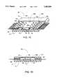
- FIGS. 1A and 1Bare a cutaway perspective view and a cross-sectional view, respectively, of a packaged integrated circuit according to an embodiment of the invention.
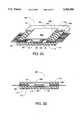
- FIGS. 1C and 1Dare a cutaway perspective view and a cross-sectional view, respectively, of a packaged integrated circuit according to another embodiment of the invention.
- FIGS. 2A and 2Bare a cutaway perspective view and a cross-sectional view, respectively, of a packaged integrated circuit according to another embodiment of the invention.
- FIGS. 2C and 2Dare a cutaway perspective view and a cross-sectional view, respectively, of a packaged integrated circuit according to another embodiment of the invention.
- FIGS. 3A and 3Bare a cutaway perspective view and a cross-sectional view, respectively, of a packaged integrated circuit according to another embodiment of the invention.
- FIGS. 4A and 4Bare a cutaway perspective view and a cross-sectional view, respectively, of a packaged integrated circuit according to another embodiment of the invention.
- FIGS. 4C to 4Fare cross-sectional views of packaged integrated circuits according to additional embodiments of the invention.
- FIGS. 5A and 5Bare a side view and plan view, respectively, of a thermal induction plate that can be used with the embodiments of the invention of FIGS. 1A, 1B, 1C, 1D, 3A and 3B.
- FIGS. 6A and 6Bare a side view and plan view, respectively, of a thermal induction plate that can be used with the embodiments of the invention of FIGS. 2A, 2B, 2C, 2D, 4A and 4B.
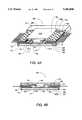
- FIG. 7Ais an exploded cross-sectional view of a partially packaged integrated circuit according to the invention.
- FIG. 7Bis a cross-sectional view of the assembled partially packaged integrated circuit of FIG. 7B.
- FIG. 8is a cross-sectional view of the assembled partially packaged integrated circuit of FIG. 7B disposed in a mold cavity of a mold assembly that is used to produce a packaged integrated circuit.
- FIGS. 1A and 1Bare a cutaway perspective view and a cross-sectional view, respectively, of a packaged integrated circuit 100 according to an embodiment of the invention.
- a semiconductor die 106 on which electrically conductive circuitry (not shown) and a plurality of electrically conductive bond pads 109 are formedis attached to a heat sink 101 with an adhesive 115.
- the inner portion of a surface of each of a plurality of electrically conductive package leads 102are attached with an electrically insulative adhesive 112 to the heat sink 101 such that inner ends of the package leads 102 are near the die 106.
- a thermal induction plate 108is positioned adjacent to a surface of each of the package leads 102 opposite the surface attached to the heat sink 101 such that the thermal induction plate 108 is electrically insulated from the package leads 102.
- the thermal induction plate 108is attached to the package leads 102 with an adhesive 114, the adhesive 114 does not have to be used. Instead, a dielectric layer could be positioned between the thermal induction plate 108 and the package leads 102.
- the thermal induction plate 108provides several benefits.
- the presence of the thermal induction plate 108reduces the inductance in signal paths, thus reducing switching noise, and reduces the capacitive coupling between adjacent signal paths, thus reducing crosstalk.
- the thermal induction plate 108shields electromagnetic energy radiated from within the packaged integrated circuit 100.
- the thermal induction plate 108also helps transfer heat away from the die 106, since heat can be conducted through the package leads 102 to the thermal induction plate 108, then through the thermal induction plate 108 and, ultimately, to the exterior of the packaged integrated circuit 100.
- the thermal induction plate 108is formed with three sections 108a, 108b, 108c. Sets of holes 116a, 116b, 116c are formed through each of the sections 108a, 108b, 108c, respectively. Though the holes 116a, 116b, 116c are shown as circular, it is to be understood that the holes 116a, 116b, 116c could have another shape, e.g., elliptical, "racetrack-shaped," etc. Further, the thermal induction plate 108 can be formed with one continuous surface or can have other than three surfaces. Additionally, the thermal induction plate 108 need not have a section extending over the die 106, e.g., the thermal induction plate 108 may include only section 108c.
- Electrically conductive bond wires 107connect selected ones of the bond pads 109 on the die 106 to an inner portion of selected ones of the package leads 102 or to bonding locations 111 on the heat sink 101. Likewise, the inner portion of some of the package leads 102 may be attached to bonding locations 111 on the heat sink 101 with bond wires 107.
- the semiconductor die 106, heat sink 101, thermal induction plate 108, inner portion of the package leads 102 and bond wires 107are enclosed in an integrated circuit package 110 such as, for instance, a plastic package formed by, for instance, injection molding, transfer molding or potting.
- the outer portions of the package leads 102extend outside the package 110 and allow electrical connection to be made between the semiconductor die 106 inside the package 110 and electronic components outside the package 110.
- the surface 101a of the heat sink 101is exposed (excepting the possible presence of encapsulant bleed or flash, as explained below) to the exterior of the package 110.
- Protrusions 108dextend from the section 108a of the thermal induction plate 108 so that the protrusions 108d are exposed to the exterior of the package 110.
- the adhesive 115 used to attach the semiconductor die 106 to the heat sink 101could be either electrically insulative or electrically conductive, depending on the desired voltage biases for the heat sink 101 and substrate of the die 106. If the heat sink 101 and substrate of the die 106 are to be biased to the same voltage, then the adhesive 115 is electrically conductive; otherwise, the adhesive 115 is electrically insulative.
- a polyimide or epoxy adhesive(to which ceramic fill may be added, if desired, to increase thermal conductivity) may be used, for instance, as an electrically insulative adhesive.
- An epoxy or polymide resin to which silver fill is addedmay be used, for instance, as an electrically conductive adhesive.
- the electrically insulative adhesive 112 used to attach the package leads 102 to the heat sink 101can be, for instance, a polyimide with a ceramic fill that is relatively thermally conductive so that heat can be more efficiently transferred from the package leads 102 to the heat sink 101 and from there to the exterior of the package 110.
- the adhesive 112extends beyond the inner end of the package leads 102. This is done to compensate for tolerances in positioning of the package leads 102 with respect to the adhesive 112 that may otherwise allow a reduction in electrical isolation (and, thus, electrical leakage) between the package leads 102 and heat sink 101.
- the extended adhesive 112also relieves stress caused by the differences in coefficients of expansion of the package materials which create stress during thermal cycling of the packaged integrated circuit 100.
- the thermal induction platemay be formed from, for example, copper or anodized aluminum. If copper is used, the choice of copper depends on the desired characteristics of the thermal induction plate 108. For instance, "pure" copper is relatively soft and easy to form, making production of the thermal induction plate relatively easy. Beryllium copper is not as easy to form as “pure” copper, but shears more cleanly, allowing the thermal induction plate to be separated more easily from the forming apparatus. Various types of aluminum alloys, beryllium copper, or other copper alloys, each having different electrical characteristics, may be used.
- the thermal induction plate 108is made of copper, then it is necessary either to use an adhesive 114 that is electrically insulative to attach the thermal induction plate 108 to the package leads 102, or to dispose a dielectric layer (not shown in FIGS. 1A and 1B) between the thermal induction plate 108 and package leads 102. Since, as discussed below, it is desirable that a large amount of heat be transferred from the package leads 102 to the thermal induction plate 108, an electrically insulative, but thermally conductive, adhesive such as ceramic-filled polyimide could be used.
- the thermal induction plate 108is made of anodized aluminum, illustratively, the thermal induction plate 108 may be black anodized aluminum 6061. Anodization increases the corrosion resistance of the thermal induction plate 108 and may be desirable for cosmetic reasons.
- Any adhesive 114is acceptable, e.g., ceramic-filled epoxy resin, to attach the anodized aluminum thermal induction plate 108 to the package leads 102.
- the thermal induction plate 108can just be placed in close proximity to the package leads 102 without being attached with the adhesive 114.
- the holes 116a, 116b, 116c in the thermal induction plate 108may be formed by etching or by a mechanical method such as stamping, cutting or drilling.
- FIGS. 1C and 1Dare a cutaway perspective view and a cross-sectional view, respectively, of a packaged integrated circuit 150 according to another embodiment of the invention.
- the packaged integrated circuit 150is the same as the packaged integrated circuit 100 except that the heat sink 101 of the packaged integrated circuit 100 is not present in the packaged integrated circuit 150. Since the heat sink 101 is no longer present, the die 106 is mounted instead to a die attach pad 113.
- FIGS. 2A and 2Bare a cutaway perspective view and a cross-sectional view, respectively, of a packaged integrated circuit 200 according to another embodiment of the invention.
- the packaged integrated circuit 200is similar to the packaged integrated circuit 100 and like elements in the packaged integrated circuits 100 and 200 are indicated with the same numbers.
- the thermal induction plate 108(FIGS. 1A and 1B) has a section 108a on which protrusions 108d are formed and through which holes 116a are formed
- the thermal induction plate 208(FIGS. 2A and 2B) has a section 208a without protrusions or holes.
- an entire surface of section 208a of thermal induction plate 208is exposed outside the package 110 of packaged integrated circuit 200.
- FIGS. 2C and 2Dare a cutaway perspective view and a cross-sectional view, respectively, of a packaged integrated circuit 250 according to another embodiment of the invention.
- the packaged integrated circuit 250is the same as the packaged integrated circuit 200 except that the heat sink 101 of the packaged integrated circuit 200 is not present in the packaged integrated circuit 250.
- the die 106is attached to the die attach pad 113 rather than the heat sink 101.
- FIGS. 3A and 3Bare a cutaway perspective view and a cross-sectional view, respectively, of a packaged integrated circuit 300 according to another embodiment of the invention.
- the packaged integrated circuit 300is similar to the packaged integrated circuit 100 and like elements in the packaged integrated circuits 100 and 300 are indicated with the same numbers.
- a generally conductive layer 305has been added to the packaged integrated circuit 100 of FIGS. 1A and 1B.
- the generally conductive layer 305which may be a layer of electrically conductive material or a layer of electrically insulative material in which electrically conductive regions and/or paths (traces) are formed, is attached on one side to the heat sink 101.
- the generally conductive layer 305is formed around the periphery of the die 106. It is to be understood that in other embodiments of the invention, the generally conductive layer 305 can be formed such that the generally conductive layer 305 also extends underneath the die 106.
- the package leads 102are attached to a side of the generally conductive layer 305 that is opposite the side to which the heat sink 101 is attached.
- the inner ends 102a of the package leads 102do not extend to the interior edge 305a of the generally conductive layer 305 since some area must be left on the generally conductive layer 305 for bonding locations 312.
- Bond wires 109are used to connect bonding locations 312 to selected ones of the package leads 102 or bond pads 109 on the die 106.
- bond wires 107are used to connect bonding locations 111 on the heat sink 101 to selected ones of the package leads 102 or bond pads 109 on the die 106.
- dielectric layer 303is disposed between the generally conductive layer 305 and the package leads 102
- dielectric layer 304is disposed between the generally conductive layer 305 and heat sink 101.
- Each of the dielectric layers 303, 304is attached with an adhesive, such as an epoxy resin, to the heat sink 101, package leads 102 or generally conductive layer 305 as appropriate.
- the dielectric layers 303 and 304electrically isolate the generally conductive layer 305 from the package leads 102 and heat sink 101, respectively.
- the dielectric layers 303, 304need not be present.
- the generally conductive layer 305may be attached to each of the package leads 102 and heat sink 101 with an electrically insulative adhesive.
- An epoxy or polyimide adhesivemay be used.
- the interior edge 303a of the dielectric layer 303extends beyond the inner ends 102a of the package leads 102. This is done to compensate for tolerances in positioning of the dielectric layer 303 and package leads 102 with respect to one another that may otherwise allow contact (and, thus, electrical shorting) between the package leads 102 and generally conductive layer 305.
- FIGS. 4A and 4Bare a cutaway perspective view and a cross-sectional view, respectively, of a packaged integrated circuit 400 according to another embodiment of the invention.
- the packaged integrated circuit 400is similar to the packaged integrated circuit 200 and like elements in the packaged integrated circuits 200 and 400 are indicated with the same numbers.
- the generally conductive layer 305has been added to the packaged integrated circuit 200 of FIGS. 2A and 2B.
- the attachments between the generally conductive layer 305 and other elements of the packaged integrated circuit 400are as described above with respect to FIG. 3.
- FIGS. 3A, 3B, 4A and 4Binclude a single generally conductive layer. It is to be understood that the invention encompasses integrated circuits that include more than one generally conductive layer.
- generally conductive layerscan be used either between the package leads and heat sink, or between the package leads and thermal induction plate. Additional dielectric layers may be provided to electrically isolate each additional generally conductive layer from the other generally conductive layers, the heat sink, the thermal induction plate, or the package leads, as appropriate.
- adhesiveis used to attach each of the additional generally conductive and dielectric layers to adjacent layers.
- the separate dielectric layersneed not be used and the generally conductive layers may be attached with an electrically insulative adhesive (which creates a dielectric layer) to other generally conductive layers, the heat sink, the thermal induction plate or the package leads.
- the number of generally conductive layersis limited by the increasing thickness of the packaged integrated circuit that results as the number of generally conductive layers increases.
- FIGS. 4C and 4Dare cross-sectional views of packaged integrated circuits 410 and 420 according to additional embodiments of the invention.
- generally conductive layer 405 and dielectric layer 404have been added between dielectric layer 304 and heat sink 101.
- dielectric layer 414 and generally conductive layerhave been added between package leads 102 and thermal induction plate 208.
- the generally conductive layer 305is connected to the package leads 102 and the die 106 with bond wires 107
- other means of making electrical connectioncan be used.
- a conductive epoxysuch as a silver filled epoxy
- through holescan be formed in the dielectric layer 303 and plated with an electrically conductive material to form electrical connection between selected package leads 102 and selected locations on the generally conductive layer 305.
- Generally conductive layerse.g., generally conductive layer 305
- packaged integrated circuitse.g., packaged integrated circuits 300 and 400
- electrically connecting the generally conductive layer to other electrically conductive material within the packaged integrated circuite.g., packaged integrated circuits 300 and 400
- Such a generally conductive layercould act as, for instance, a floating electrical plane.
- the generally conductive layerstill provides electrical benefits such as reduction of package lead mutual inductance.
- the generally conductive layer or layersare shown formed around the periphery of the semiconductor die, it is to be understood that one or more of the generally conductive layers can be formed to extend underneath the die.
- FIGS. 4E and 4Fare cross-sectional views of a portion of packaged integrated circuits 430 and 440, respectively, in which the thermal induction plate 108 or 408, respectively is electrically connected to selected package leads 102.
- the thermal induction platecan be, for instance, a ground plane or power plane.
- packaged integrated circuits 430 and 440are similar to packaged integrated circuit 150 of FIGS. 1C and 1D, and like elements are designated by the same numerals.
- adhesive 414 attaching package leads 102 to thermal induction plate 108is shorter than the corresponding adhesive 114 in packaged integrated circuit 150.
- a ball bond 431is formed, using conventional wirebonding equipment, on package leads 102 that are to be electrically connected to thermal induction plate 108. Ball bonds 431 are formed on the selected package leads 102 between edge 414a of the adhesive 414 and the edge of package 110.
- adhesive 414could be made shorter at edge 414b so that a surface of section 108c facing package leads 102 is exposed. Ball bonds 431 could then be formed on the selected package leads 102 adjacent edge 414b of adhesive 414.
- thermal induction plate 408is formed with dimples 408a at locations that are aligned with package leads 102 to which it is desired to make electrical connection.
- Dimples 408acan be formed by a punch and mating female die.
- dimples 408acan be formed on either side of adhesive 414 with appropriate sizing of adhesive 414.
- FIGS. 3A, 3B, 4A, 4B, 4C and 4Dall include a heat sink 101, it is to be understood that packaged integrated circuits according to the invention can be formed as in FIGS. 3A, 3B, 4A, 4B, 4C and 4D with the heat sink 101 omitted.
- FIGS. 5A and 5Bare a side view and plan view, respectively, of a thermal induction plate 508 that can be used with embodiments of the invention in which the only parts of the thermal induction plate 508 that are exposed to the exterior of the integrated circuit package are protrusions 508g.
- the dimensions 509a, 509b and 509c of the thermal induction plate 509are 0.020 inches (0.50 mm), 0.0354 inches (0.90 mm) and 0.0634 inches (1.61 mm), respectively.
- the dimension 509cis measured to the end of the protrusions 508g.
- the dimensions 509d, 509e and 509f of the thermal induction plate 509are 1.10 inches (27.9 mm), 0.772 inches (19.6 mm) and 0.693 inches (17.6 mm), respectively.
- the radius of curvature of the rounded corners 508his 0.0846 inches (2.15 mm).
- the dimension 509dis measured from the outermost point of two corners 508h.
- the sides 508jare slightly recessed relative to the outermost point of the corners 508h so that the distance between the outermost points of the sides 508j is 1.08 inches (27.6 mm).
- the sides 508jare castellated so that, during formation of a packaged integrated circuit including the thermal induction plate 508 as described below with respect to FIG. 8, the package material can flow past the sides of the thermal induction plate 508.
- the holes 508d formed through the section 508ahave a diameter of 0.0354 inches (0.90 mm).
- the holes 508e formed through the section 508bhave a diameter of 0.030 inches (0.76 mm).
- the holes 508f formed through the section 508chave a diameter of 0.030 inches (0.76 mm).
- the holesare formed such that approximately equal amounts of thermal induction plate 508 remain above each package lead in the packaged integrated circuit for which the thermal induction plate 508 is intended, while providing for good flow of molding compound in and around the package leads without entrapment of air.
- the holes 508d, 508e, 508fare located and sized so that the thermal induction plate 508 will interact with other electrically conductive parts of the packaged integrated circuit (e.g., package leads, die, generally conductive layer) to provide the desired electrical characteristics.
- the packaged integrated circuite.g., package leads, die, generally conductive layer
- the protrusions 508ghave a height that is adequate to ensure that the thermal induction plate 508 will be covered with package material when encapsulated in a packaged integrated circuit. The exact height depends on the properties of the package material used.
- the protrusions 508gcan be cylindrical, conical or any other desired shape. In FIG. 5, each of the protrusions 508g is formed on section 508a approximately midway along a side of section 508a; however, the protrusions 508g can be formed at any locations.
- FIGS. 6A and 6Bare a side view and plan view, respectively, of a thermal induction plate 608 that can be used with embodiments of the invention in which an entire surface of section 608a is exposed to the exterior of the integrated circuit package.
- Corresponding dimensions of the thermal induction plates 508 and 608are the same, except that the dimension of the thermal induction plate 608 that corresponds to the dimension 509b is 0.0434 inches (1.10 mm).
- the dimension of the thermal induction plate 608 that corresponds to the dimension 509c of the thermal induction plate 509is measured to the exposed surface of section 608a.
- the inventionencompasses thermal induction plates having dimensions different than those given above for the thermal induction plates 508 and 608.
- the size, number and location of the holesmay be varied, the size and shape of the sections may be varied, and the thicknesses of different sections and overall thickness of the thermal induction plate may be varied.
- thermal induction plates according to the inventionare sized according to the particular mold cavity and package used.
- the size, shape and location of the holes in the thermal induction plateinvolves a tradeoff between achieving good flow of the package material during formation of a packaged integrated circuit according to the invention, as described below, maintaining a large area of metal to provide better thermal and electrical characteristics, and providing adequate strength to withstand stress.
- Packaged integrated circuits 100, 200, 300 and 400including a heat sink 101 dissipate heat particularly effectively.
- the adhesive 115 used to attach the die 106 to the heat sink 101is relatively thin and thermally conductive; therefore, the adhesive 115 does not represent a significant thermal barrier to the transfer of heat from the die 106 to the heat sink 101.
- the close connection between the die 106 and heat sink 101allows a large amount of heat to be transferred from the die 106 to the heat sink 101. This heat is then conducted through the heat sink 101 and convected and radiated away from the packaged integrated circuit 100, 200, 300 or 400 at the surface 101a of the heat sink 101 exposed to the exterior of the package 110, or conducted through the package leads 102 to the exterior of the package 120.
- the exposed heat sink surface 101aallows heat to be transferred from the heat sink 101 away from the packaged integrated circuit 100, 200, 300 or 400 better than would be the case if relatively thermally insulative package material covered the heat sink surface 101a, impeding the transfer of heat from the packaged integrated circuit 100, 200, 300 or 400.
- the thermal induction plate 108 or 208aids in the transfer of heat away from the die 106. Heat is transferred to the package leads 102 from the die 106 through the bond wires 107 and, in the packaged integrated circuits 100 and 200, through the heat sink 101. Some of this heat is then transferred to the thermal induction plate 108 or 208 (the remainder is transferred through the package leads 102 to the exterior of the package 110). The heat transferred to the thermal induction plate 108 or 08 is conducted through the thermal induction plate 108 or 208. This heat is then convected and radiated away from the exposed surface of section 208a of the thermal induction plate 208 in packaged integrated circuits 200, 250 and 400.
- this heatis convected and radiated away from the protrusions 108d exposed to the exterior of the package 110, or it is conducted through the relatively thin layer of package material lying between the thermal induction plate 108 and the exterior of the package 110, then convected and radiated away from the packaged integrated circuit 100, 150 or 300.
- packaged integrated circuits according to the inventione.g., packaged integrated circuits 100, 150, 200, 250, 300 and 400
- the presence of the thermal induction plate 108 or 208 in proximity to the package leads 102causes mutual inductance between the package leads 102 and thermal induction plate 108 or 208, resulting in a reduction of inductance in signal paths (particularly power and ground paths), thereby reducing switching noise in the packaged integrated circuits 100, 150, 200, 250, 300 and. 400.
- the presence of the thermal induction plate 108 or 208also reduces the capacitive coupling between adjacent signal paths in the packaged integrated circuits 100, 150, 200, 250, 300 and 400, thereby reducing crosstalk.
- the generally conductive layer 305can be used to provide a ground plane, power plane, signal routing, or some combination of these functions. Consequently, the packaged integrated circuits 300 and 400 have a high degree of flexibility in electrical design and reduced electrical noise as compared to previous packaged integrated circuits. For instance, provision of power and/or ground planes on the generally conductive layer 305 enables uniform power and ground supplies to be provided to the circuitry formed on the die 106. The presence of the generally conductive layer 305 reduces the inductance of package leads 102, which results in a reduction of electrical noise. The power and ground planes also provide decoupling capacitances that reduce switching noise and crosstalk. Provision of signal routing on the generally conductive layer 305 allows increased flexibility in signal routing for single chip packaged integrated circuits 100, 200, 300 or 400 and may be used for connecting chips and passive components in multichip or hybrid modules.
- the heat sink 101 in packaged integrated circuits 100, 150, 200, 250, 300 and 400can also perform an electrical function.
- the heat sink 101may be used as a ground or power plane. If the heat sink 101 performs an electrical function in the packaged integrated circuit 100, 150, 200, 250, 300 or 400, bonding locations 111 on the heat sink 101 are electrically connected to one or more bond pads 109 on the die 106, or one or more package leads 102.
- Integrated circuits according to the inventionmay be formed using any of a number of well-known techniques. Below, an illustrative method for constructing an integrated circuit according to the invention is briefly described.
- FIG. 7Ais an exploded cross-sectional view of a partially packaged integrated circuit 400.
- the partially packaged integrated circuit 400includes a semiconductor die 106, a heat sink 101, package leads 102 of a leadframe, and a "sandwich" 710 including generally conductive layer 305 assembled between dielectric layers 303 and 304.
- the sandwich 710is formed with a rectangular hole in its center so that in the packaged integrated circuit 400, the sandwich 710 surrounds the periphery of the semiconductor die 106.
- the sandwich 710may be formed in the following manner.
- Dielectric layers 303 and 304made of, for instance, polyimide, are coated with adhesive, such as epoxy resin, by, for instance, roll coating.
- adhesivesuch as epoxy resin
- the dielectric layers 303, 304can be purchased from a vendor with adhesive, such as epoxy adhesive, already applied to both sides of the dielectric layers 2303, 304.
- the generally conductive layer 305is placed on the dielectric layer 304 such that an adhesive-coated side of the dielectric layer 304 faces the generally conductive layer 305. While heat is applied, the dielectric layer 304 and generally conductive layer 305 are squeezed together by, for instance, a mechanical press. The application of heat causes the adhesive to become tacky. The dielectric layer 304 and generally conductive layer 305 are allowed to cool to room temperature, solidifying the adhesive and bonding the dielectric layer 304 to the generally conductive layer 305.
- a desired patternis etched and a hole is punched through the dielectric layer 304 and generally conductive layer 305.
- the holeis stamped using a conventional punch.
- a larger holeis formed through the dielectric layer 303. The dielectric layer 303 is aligned, then attached to the generally conductive layer 305 in the manner described above for the dielectric layer 304 and generally conductive layer 305.
- conductive regions and pathscould be formed on (additive process), or etched from (substractive process), the generally conductive layer 305 either before the attachment of the generally conductive layer 305 to the dielectric layers 303, 304 or after the attachment of the dielectric layer 304. If after, the electrically conductive traces and regions would, of course, be formed on, or etched from, the surface of the generally conductive layer 305 not attached to the dielectric layer 304.
- the dielectric layer 304 of the sandwich 710is attached to the heat sink 101, the package leads 102 of the leadframe are attached to the dielectric layer 303 of the sandwich 710, and the semiconductor die 106 is attached to the heat sink 101 with adhesives.
- the adhesivesbond the heat sink 101, sandwich 710, die 106 and leadframe by being heated to become tacky, then cooled to solidify.
- Each of the attachments--sandwich 710 to heat sink 101, package leads 102 to sandwich 710, die 106 to heat sink 101--couldbe performed simultaneously or sequentially (one at a time or two at a time) in a desired order.
- the sandwich 710is attached to the package leads 102 and the heat sink 101, then the die 106 is attached to the heat sink 101.
- Selected package leads 102are bonded using conventional wirebonding techniques to bond pads on the die 106, bonding locations 312 on the generally conductive layer 305, or bonding locations 111 on the heat sink 101, respectively.
- selected bond pads on the die 106are bonded to package leads 102, bonding locations 312 on the generally conductive layer 305, or bonding locations 111 on the heat sink 101, respectively.
- other die interconnection technologiessuch as TAB, can be used.
- the partially packaged integrated circuit 400, as assembled at this point,is shown in FIG. 7B.
- FIG. 8is a cross-sectional view of the partially packaged integrated circuit 400 disposed in a mold cavity 845 of a mold assembly 840 that is used to produce a packaged integrated circuit.
- the thermal induction plate 208(the holes in thermal induction plate 208 are not shown to increase the clarity of FIG. 8) is dropped into the mold cavity 845 so that a surface of section 208a contacts the surface 841a of the mold half 841.
- the thermal induction plate 208Since the dimensions of the thermal induction plate 208 (measured in a plane parallel to the surface 841a extending between the edges 808a of the thermal induction plate 208) are just slightly less (e.g., 0.012 inches (0.3 mm)) than the corresponding dimensions of the cavity 845, the thermal induction plate 208 self-aligns within the mold cavity 845. This self-alignment allows use of the drop-in technique for disposing the thermal induction plate 208 within the mold cavity 845.
- a dielectric and/or adhesiveis placed between the thermal induction plate 208 and the package leads 102 by pre-attaching to either the thermal induction plate 208 or the package leads 102.
- the partially packaged integrated circuit 400is disposed within the mold cavity 845 on top of the thermal induction plate 208 and is located and held in place by pins 846 formed on the mold half 841 that fit through holes 702a formed at intervals in the frame of the leadframe.
- the thermal induction plate 208may be attached to the package leads 102 prior to being inserted into the mold cavity 845.
- the two mold halves 841 and 842are brought together. Just prior to closure of the mold 840, the surface 842a of the mold half 842 contacts the surface 101a of the heat sink 101.
- the combined thickness of the heat sink 101, dielectric layers 303 and 304, and generally conductive layer 305is intentionally made slightly greater than the dimension 845a of the upper half of the mold cavity 845.
- the closing motion of the mold half 842forces the combination of the heat sink 101, dielectric layers 303 and 304, and generally conductive layer 305 downward just prior to mold closure. Since the package leads 102 are held in place by the pins 846, this downward motion causes the inner portions of the package leads 102 to bend slightly downward.
- This bending of the package leads 102gives rise to tensile forces in the package leads 102 that act to counteract the movement of the heat sink 101, dielectric layers 303 and 304, and generally conductive layer 305, and maintain contact between surface 101 a of heat sink 101 and mold surface 842a.
- the bent package leads 102also force the surface of section 208a of the thermal induction plate 208 against the mold surface 841a.
- encapsulantis pressure fed by, for instance, transfer molding or injection molding, into the mold cavity 845 until the cavity 845 is full.
- the encapsulantis fed into the cavity 845 through the channel 848 in a method known as bottom side gating.
- Other gating methodscould be used for transferring encapsulant into the mold cavity 845, e.g., gang pot, top plane gating, bottom plane gating.
- the encapsulantis allowed to cool and solidify.
- the mold assembly 840is then opened and the packaged integrated circuit 400 removed.
- the presence of the holes 116b and 116c in the thermal induction plates 108 and 208allow encapsulant to flow past the thermal induction plate 108 or 208 to the area around the die 106 so that cavities do not form in the hardened encapsulant. Additionally, the hardening of the encapsulant through the holes 116b and 116c locks the package 110 to the remainder of the packaged integrated circuit 100, 150, 200, 250, 300 or 400 better than would otherwise be the case. In packaged integrated circuits 100, 150 and 300 in which the thermal induction plate 108 is used, the additional holes 116a in the thermal induction plate 108 further aid encapsulant flow to the region around the die 106 and provide additional locking of the encapsulant to the rest of the packaged integrated circuit 100, 150 or 300.
- encapsulant bleedthe undesirable presence of translucent encapsulant
- encapsulant flashthe undesirable presence of encapsulant greater in thickness than bleed and visible to the naked eye
- outer portions of the package leads 102extend outside the package and are connected to each other by the frame of the leadframe.
- the package leads 102are physically separated by removing the portions of the frame between package leads 102.
- the individual package leads 102may then be bent, if desired, into a position that allows surface mounting of the packaged integrated circuit 400.
- each integrated circuit according to the inventionmay have package leads or exterior package connections extending from any number of sides of the package or, more generally, in any manner from the exterior of the package.
Landscapes
- Engineering & Computer Science (AREA)
- Power Engineering (AREA)
- Computer Hardware Design (AREA)
- Microelectronics & Electronic Packaging (AREA)
- Physics & Mathematics (AREA)
- General Physics & Mathematics (AREA)
- Condensed Matter Physics & Semiconductors (AREA)
- Health & Medical Sciences (AREA)
- Electromagnetism (AREA)
- Toxicology (AREA)
- Manufacturing & Machinery (AREA)
- Lead Frames For Integrated Circuits (AREA)
- Cooling Or The Like Of Semiconductors Or Solid State Devices (AREA)
Abstract
Description
Claims (19)
Priority Applications (1)
| Application Number | Priority Date | Filing Date | Title |
|---|---|---|---|
| US08/411,010US5482898A (en) | 1993-04-12 | 1995-03-27 | Method for forming a semiconductor device having a thermal dissipator and electromagnetic shielding |
Applications Claiming Priority (2)
| Application Number | Priority Date | Filing Date | Title |
|---|---|---|---|
| US4888893A | 1993-04-12 | 1993-04-12 | |
| US08/411,010US5482898A (en) | 1993-04-12 | 1995-03-27 | Method for forming a semiconductor device having a thermal dissipator and electromagnetic shielding |
Related Parent Applications (1)
| Application Number | Title | Priority Date | Filing Date |
|---|---|---|---|
| US4888893ADivision | 1993-04-12 | 1993-04-12 |
Publications (1)
| Publication Number | Publication Date |
|---|---|
| US5482898Atrue US5482898A (en) | 1996-01-09 |
Family
ID=21956982
Family Applications (2)
| Application Number | Title | Priority Date | Filing Date |
|---|---|---|---|
| US08/411,010Expired - LifetimeUS5482898A (en) | 1993-04-12 | 1995-03-27 | Method for forming a semiconductor device having a thermal dissipator and electromagnetic shielding |
| US08/410,381Expired - LifetimeUS5485037A (en) | 1993-04-12 | 1995-03-27 | Semiconductor device having a thermal dissipator and electromagnetic shielding |
Family Applications After (1)
| Application Number | Title | Priority Date | Filing Date |
|---|---|---|---|
| US08/410,381Expired - LifetimeUS5485037A (en) | 1993-04-12 | 1995-03-27 | Semiconductor device having a thermal dissipator and electromagnetic shielding |
Country Status (1)
| Country | Link |
|---|---|
| US (2) | US5482898A (en) |
Cited By (49)
| Publication number | Priority date | Publication date | Assignee | Title |
|---|---|---|---|---|
| US5629561A (en)* | 1994-12-16 | 1997-05-13 | Anam Industrial Co., Ltd. | Semiconductor package with integral heat dissipator |
| US5679604A (en)* | 1995-04-04 | 1997-10-21 | Hughes Aircraft Company | Wire diamond lattice structure for phased array side lobe suppression and fabrication method |
| DE19620517A1 (en)* | 1996-05-22 | 1997-11-27 | Berud Dipl Ing Koeppe | Forcibly ventilated cooler device for power semiconductor of electrical machine |
| US5843808A (en)* | 1996-01-11 | 1998-12-01 | Asat, Limited | Structure and method for automated assembly of a tab grid array package |
| US5930072A (en)* | 1997-05-06 | 1999-07-27 | Seagate Technology, Inc. | Head-disk assembly for reducing noise coupled into magnetoresistive head preamplifiers |
| US6064286A (en)* | 1998-07-31 | 2000-05-16 | The Whitaker Corporation | Millimeter wave module with an interconnect from an interior cavity |
| US6114190A (en)* | 1998-04-14 | 2000-09-05 | Micron Technology, Inc. | Method of forming heat sink and semiconductor chip assemblies |
| US6291263B1 (en)* | 2000-06-13 | 2001-09-18 | Siliconware Precision Industries Co., Ltd. | Method of fabricating an integrated circuit package having a core-hollowed encapsulation body |
| US6304441B1 (en) | 1998-08-20 | 2001-10-16 | Sansung Electronics Co., Ltd. | Radiation apparatus and radiation method for integrated circuit semiconductor device and for portable computer |
| US6400014B1 (en)* | 2001-01-13 | 2002-06-04 | Siliconware Precision Industries Co., Ltd. | Semiconductor package with a heat sink |
| US6429513B1 (en) | 2001-05-25 | 2002-08-06 | Amkor Technology, Inc. | Active heat sink for cooling a semiconductor chip |
| US20020119602A1 (en)* | 2001-02-23 | 2002-08-29 | Masahiro Yonemochi | Insert-moldable heat spreader, semiconductor device using same, and method for manufacturing such semiconductor device |
| US6504256B2 (en)* | 2001-01-30 | 2003-01-07 | Bae Systems Information And Electronic Systems Integration, Inc. | Insitu radiation protection of integrated circuits |
| US6528876B2 (en)* | 2000-06-26 | 2003-03-04 | Siliconware Precision Industries Co., Ltd. | Semiconductor package having heat sink attached to substrate |
| US20030143781A1 (en)* | 2002-01-31 | 2003-07-31 | Mclellan Neil Robert | Encapsulated integrated circuit package and method of manufacturing an integrated circuit package |
| US20030178719A1 (en)* | 2002-03-22 | 2003-09-25 | Combs Edward G. | Enhanced thermal dissipation integrated circuit package and method of manufacturing enhanced thermal dissipation integrated circuit package |
| US6627999B2 (en) | 2000-08-31 | 2003-09-30 | Micron Technology, Inc. | Flip-chip with matched signal lines, ground plane and ground bumps adjacent signal bumps |
| US20030234454A1 (en)* | 2002-06-24 | 2003-12-25 | Serafin Pedron | Integrated circuit package and method of manufacturing the integrated circuit package |
| US20040014508A1 (en)* | 2002-06-24 | 2004-01-22 | Seo Dong Han | Apparatus for improving reception sensitivity of public wave receiver |
| US6713879B2 (en) | 2000-08-31 | 2004-03-30 | Micron Technology, Inc. | Semiconductor substract with substantially matched lines |
| US20040070069A1 (en)* | 2000-11-14 | 2004-04-15 | Jai Subramanian | Lid and heat spreader design for a semiconductor package |
| US20040079862A1 (en)* | 2001-01-10 | 2004-04-29 | Silverbrook Research Pty Ltd | Two part mold for wafer scale caps |
| US6734552B2 (en) | 2001-07-11 | 2004-05-11 | Asat Limited | Enhanced thermal dissipation integrated circuit package |
| US20040207082A1 (en)* | 2003-04-15 | 2004-10-21 | Shinko Electric Industries Co., Ltd. | Semiconductor package and production method |
| US20040222433A1 (en)* | 2003-05-05 | 2004-11-11 | Lamina Ceramics | Light emitting diodes packaged for high temperature operation |
| US20050012203A1 (en)* | 2001-02-15 | 2005-01-20 | Rahman Khan Reza-Ur | Enhanced die-down ball grid array and method for making the same |
| US6919631B1 (en) | 2001-12-07 | 2005-07-19 | Amkor Technology, Inc. | Structures for improving heat dissipation in stacked semiconductor packages |
| US20050174544A1 (en)* | 2003-05-05 | 2005-08-11 | Joseph Mazzochette | LED light sources for image projection systems |
| US20050189557A1 (en)* | 2004-02-26 | 2005-09-01 | Joseph Mazzochette | Light emitting diode package assembly that emulates the light pattern produced by an incandescent filament bulb |
| US20050225222A1 (en)* | 2004-04-09 | 2005-10-13 | Joseph Mazzochette | Light emitting diode arrays with improved light extraction |
| US20060006405A1 (en)* | 2003-05-05 | 2006-01-12 | Lamina Ceramics, Inc. | Surface mountable light emitting diode assemblies packaged for high temperature operation |
| US20060012986A1 (en)* | 2004-07-19 | 2006-01-19 | Joseph Mazzochette | LED array package with internal feedback and control |
| US7015072B2 (en) | 2001-07-11 | 2006-03-21 | Asat Limited | Method of manufacturing an enhanced thermal dissipation integrated circuit package |
| US20060186423A1 (en)* | 2003-05-05 | 2006-08-24 | Greg Blonder | Method of making optical light engines with elevated LEDs and resulting product |
| US7126218B1 (en)* | 2001-08-07 | 2006-10-24 | Amkor Technology, Inc. | Embedded heat spreader ball grid array |
| US20060267184A1 (en)* | 1997-07-02 | 2006-11-30 | Kinsman Larry D | Varied-thickness heat sink for integrated circuit (IC) package |
| US20070018175A1 (en)* | 2003-05-05 | 2007-01-25 | Joseph Mazzochette | Light emitting diodes with improved light collimation |
| US20070267734A1 (en)* | 2006-05-16 | 2007-11-22 | Broadcom Corporation | No-lead IC packages having integrated heat spreader for electromagnetic interference (EMI) shielding and thermal enhancement |
| US20090183855A1 (en)* | 2007-12-21 | 2009-07-23 | Shinko Electric Industries Co., Ltd. | Heat radiating plate for semiconductor package and plating method thereof |
| US20110124158A1 (en)* | 2005-12-09 | 2011-05-26 | Fairchild Semiconductor Corporation | Thermal enhanced upper and dual heat sink exposed molded leadless package |
| US20110260314A1 (en)* | 2010-04-27 | 2011-10-27 | Stmicroelectronics S.R.L. | Die package and corresponding method for realizing a double side cooling of a die package |
| US20140220736A1 (en)* | 2011-06-16 | 2014-08-07 | Samsung Electro-Mechanics Co., Ltd. | Power module package and method for fabricating the same |
| US20140345929A1 (en)* | 2011-12-20 | 2014-11-27 | Kyocera Corporation | Electronic component housing package and electronic apparatus |
| CN104425404A (en)* | 2013-08-28 | 2015-03-18 | 英飞凌科技股份有限公司 | Packaged semiconductor device |
| US20160071777A1 (en)* | 2013-03-28 | 2016-03-10 | Panasonic Intellectual Property Management Co., Ltd. | Semiconductor package and semiconductor device |
| US20160227679A1 (en)* | 2015-01-30 | 2016-08-04 | Laird Technologies, Inc. | Board Level Electromagnetic Interference (EMI) Shields With Increased Under-Shield Space |
| US9728510B2 (en) | 2015-04-10 | 2017-08-08 | Analog Devices, Inc. | Cavity package with composite substrate |
| US10083899B2 (en)* | 2017-01-23 | 2018-09-25 | Infineon Technologies Ag | Semiconductor package with heat slug and rivet free die attach area |
| US20240258245A1 (en)* | 2023-01-26 | 2024-08-01 | Texas Instruments Incorporated | Molded module package with an emi shielding barrier |
Families Citing this family (85)
| Publication number | Priority date | Publication date | Assignee | Title |
|---|---|---|---|---|
| US5514327A (en)* | 1993-12-14 | 1996-05-07 | Lsi Logic Corporation | Powder metal heat sink for integrated circuit devices |
| US5959840A (en)* | 1994-05-17 | 1999-09-28 | Tandem Computers Incorporated | Apparatus for cooling multiple printed circuit board mounted electrical components |
| KR100201380B1 (en)* | 1995-11-15 | 1999-06-15 | 김규현 | Heat Dissipation Structure of BGA Semiconductor Package |
| US5814536A (en)* | 1995-12-27 | 1998-09-29 | Lsi Logic Corporation | Method of manufacturing powdered metal heat sinks having increased surface area |
| JPH09260550A (en)* | 1996-03-22 | 1997-10-03 | Mitsubishi Electric Corp | Semiconductor device |
| US5773895A (en)* | 1996-04-03 | 1998-06-30 | Intel Corporation | Anchor provisions to prevent mold delamination in an overmolded plastic array package |
| US5723906A (en)* | 1996-06-07 | 1998-03-03 | Hewlett-Packard Company | High-density wirebond chip interconnect for multi-chip modules |
| US6730991B1 (en)* | 1996-06-11 | 2004-05-04 | Raytheon Company | Integrated circuit chip package |
| US6429120B1 (en)* | 2000-01-18 | 2002-08-06 | Micron Technology, Inc. | Methods and apparatus for making integrated-circuit wiring from copper, silver, gold, and other metals |
| US6001672A (en)* | 1997-02-25 | 1999-12-14 | Micron Technology, Inc. | Method for transfer molding encapsulation of a semiconductor die with attached heat sink |
| JPH10294401A (en)* | 1997-04-21 | 1998-11-04 | Matsushita Electric Ind Co Ltd | Package and semiconductor device |
| US6054754A (en) | 1997-06-06 | 2000-04-25 | Micron Technology, Inc. | Multi-capacitance lead frame decoupling device |
| US5835355A (en)* | 1997-09-22 | 1998-11-10 | Lsi Logic Corporation | Tape ball grid array package with perforated metal stiffener |
| US5869883A (en)* | 1997-09-26 | 1999-02-09 | Stanley Wang, President Pantronix Corp. | Packaging of semiconductor circuit in pre-molded plastic package |
| US5880520A (en)* | 1998-03-31 | 1999-03-09 | Micron Technology, Inc. | Low mutual inductance lead frame device |
| US5949649A (en)* | 1998-04-28 | 1999-09-07 | Spectrian, Inc. | High power semiconductor device having bolt-down ceramic platform |
| US6509590B1 (en)* | 1998-07-20 | 2003-01-21 | Micron Technology, Inc. | Aluminum-beryllium alloys for air bridges |
| AU5126699A (en)* | 1998-07-22 | 2000-02-14 | Digirad Corporation | Blind pin placement on circuit boards |
| US6583987B2 (en)* | 1999-02-26 | 2003-06-24 | Intel Corporation | Electromagnetic interference and heatsinking |
| US6052045A (en)* | 1999-03-12 | 2000-04-18 | Kearney-National, Inc. | Electromechanical switching device package with controlled impedance environment |
| US6256200B1 (en)* | 1999-05-27 | 2001-07-03 | Allen K. Lam | Symmetrical package for semiconductor die |
| TW526701B (en)* | 1999-08-26 | 2003-04-01 | Rohm Co Ltd | Electromagnetic shield cap and infrared data communication module |
| AU2001229547A1 (en)* | 2000-01-18 | 2001-07-31 | Sunrisetek, Llc | Dual-sided, surface mountable integrated circuit package |
| US6420262B1 (en)* | 2000-01-18 | 2002-07-16 | Micron Technology, Inc. | Structures and methods to enhance copper metallization |
| US7262130B1 (en)* | 2000-01-18 | 2007-08-28 | Micron Technology, Inc. | Methods for making integrated-circuit wiring from copper, silver, gold, and other metals |
| US7211512B1 (en)* | 2000-01-18 | 2007-05-01 | Micron Technology, Inc. | Selective electroless-plated copper metallization |
| US6373126B1 (en)* | 2000-04-26 | 2002-04-16 | Advanced Micro Devices, Inc. | Method for reducing IC package delamination by use of internal baffles |
| US6423629B1 (en)* | 2000-05-31 | 2002-07-23 | Kie Y. Ahn | Multilevel copper interconnects with low-k dielectrics and air gaps |
| US6674167B1 (en)* | 2000-05-31 | 2004-01-06 | Micron Technology, Inc. | Multilevel copper interconnect with double passivation |
| US6512675B1 (en)* | 2000-06-28 | 2003-01-28 | Advanced Micro Devices, Inc. | Heat sink grounded to a grounded package lid |
| DE10031843A1 (en)* | 2000-06-30 | 2002-01-10 | Alcatel Sa | Electrical or opto-electrical component with a plastic packaging and method for varying the impedance of a connection line of such a component |
| USRE38381E1 (en) | 2000-07-21 | 2004-01-13 | Kearney-National Inc. | Inverted board mounted electromechanical device |
| US6403401B1 (en)* | 2000-08-14 | 2002-06-11 | St Assembly Test Services Pte Ltd | Heat spreader hole pin 1 identifier |
| US6445583B1 (en) | 2001-01-26 | 2002-09-03 | Laird Technologies, Inc. | Snap in heat sink shielding lid |
| US6501171B2 (en) | 2001-01-30 | 2002-12-31 | International Business Machines Corporation | Flip chip package with improved cap design and process for making thereof |
| US6512295B2 (en) | 2001-03-01 | 2003-01-28 | International Business Machines Corporation | Coupled-cap flip chip BGA package with improved cap design for reduced interfacial stresses |
| US7220615B2 (en)* | 2001-06-11 | 2007-05-22 | Micron Technology, Inc. | Alternative method used to package multimedia card by transfer molding |
| US6740959B2 (en) | 2001-08-01 | 2004-05-25 | International Business Machines Corporation | EMI shielding for semiconductor chip carriers |
| JP3888439B2 (en)* | 2002-02-25 | 2007-03-07 | セイコーエプソン株式会社 | Manufacturing method of semiconductor device |
| EP1483769B1 (en)* | 2002-03-08 | 2007-09-19 | Kearney-National, Inc. | Surface mount molded relay package and method of manufacturing same |
| US6744640B2 (en)* | 2002-04-10 | 2004-06-01 | Gore Enterprise Holdings, Inc. | Board-level EMI shield with enhanced thermal dissipation |
| JP3923368B2 (en)* | 2002-05-22 | 2007-05-30 | シャープ株式会社 | Manufacturing method of semiconductor device |
| TWI286832B (en)* | 2002-11-05 | 2007-09-11 | Advanced Semiconductor Eng | Thermal enhance semiconductor package |
| US20040166606A1 (en)* | 2003-02-26 | 2004-08-26 | David Forehand | Low temperature wafer-level micro-encapsulation |
| CN101789482B (en)* | 2003-03-10 | 2013-04-17 | 丰田合成株式会社 | Solid element device and method for manufacture thereof |
| US20050104164A1 (en)* | 2003-11-14 | 2005-05-19 | Lsi Logic Corporation | EMI shielded integrated circuit packaging apparatus method and system |
| JP4238126B2 (en)* | 2003-12-25 | 2009-03-11 | ローム株式会社 | Semiconductor module |
| US7091594B1 (en)* | 2004-01-28 | 2006-08-15 | Amkor Technology, Inc. | Leadframe type semiconductor package having reduced inductance and its manufacturing method |
| US7420809B2 (en)* | 2004-06-22 | 2008-09-02 | Lsi Corporation | Heat spreader in integrated circuit package |
| TWI246760B (en)* | 2004-12-22 | 2006-01-01 | Siliconware Precision Industries Co Ltd | Heat dissipating semiconductor package and fabrication method thereof |
| US20060237829A1 (en)* | 2005-04-26 | 2006-10-26 | Eiichi Hosomi | Method and system for a semiconductor package with an air vent |
| US7262369B1 (en) | 2006-03-09 | 2007-08-28 | Laird Technologies, Inc. | Combined board level EMI shielding and thermal management |
| US20080080160A1 (en)* | 2005-12-16 | 2008-04-03 | Laird Technologies, Inc. | Emi shielding assemblies |
| US7623360B2 (en)* | 2006-03-09 | 2009-11-24 | Laird Technologies, Inc. | EMI shielding and thermal management assemblies including frames and covers with multi-position latching |
| US7463496B2 (en)* | 2006-03-09 | 2008-12-09 | Laird Technologies, Inc. | Low-profile board level EMI shielding and thermal management apparatus and spring clips for use therewith |
| US7317618B2 (en)* | 2006-03-09 | 2008-01-08 | Laird Technologies, Inc. | Combined board level shielding and thermal management |
| US20080002384A1 (en)* | 2006-06-30 | 2008-01-03 | Motorola, Inc. | Apparatus for providing radio frequency shielding and heat dissipation for electronic components |
| JP4110189B2 (en)* | 2006-12-13 | 2008-07-02 | インターナショナル・ビジネス・マシーンズ・コーポレーション | Semiconductor package |
| US20100091462A1 (en)* | 2007-02-15 | 2010-04-15 | Nec Corporation | Electronic device-mounted apparatus and noise suppression method for same |
| KR100930095B1 (en)* | 2007-06-01 | 2009-12-07 | 삼성전자주식회사 | Package using printed circuit board with air vent and printed circuit board with air vent |
| US8493748B2 (en)* | 2007-06-27 | 2013-07-23 | Stats Chippac Ltd. | Packaging system with hollow package and method for the same |
| US20090002949A1 (en)* | 2007-06-29 | 2009-01-01 | Lucent Technologies Inc. | Heat transfer for electronic component via an electromagnetic interference (emi) shield having shield deformation |
| US8502371B2 (en)* | 2007-12-27 | 2013-08-06 | Stats Chippac Ltd. | Integrated circuit package system with extended corner leads |
| US8072047B2 (en)* | 2008-05-21 | 2011-12-06 | Stats Chippac Ltd. | Integrated circuit package system with shield and tie bar |
| CN102150075A (en)* | 2008-10-01 | 2011-08-10 | 夏普株式会社 | Electronic apparatus, illuminating device, display device and television receiver |
| US7965514B2 (en) | 2009-06-05 | 2011-06-21 | Laird Technologies, Inc. | Assemblies and methods for dissipating heat from handheld electronic devices |
| US8477499B2 (en) | 2009-06-05 | 2013-07-02 | Laird Technologies, Inc. | Assemblies and methods for dissipating heat from handheld electronic devices |
| WO2010143273A1 (en)* | 2009-06-10 | 2010-12-16 | トヨタ自動車株式会社 | Semiconductor device |
| US8084300B1 (en) | 2010-11-24 | 2011-12-27 | Unisem (Mauritius) Holdings Limited | RF shielding for a singulated laminate semiconductor device package |
| JP5751079B2 (en)* | 2011-08-05 | 2015-07-22 | 富士通セミコンダクター株式会社 | Semiconductor device and manufacturing method thereof |
| US8622278B1 (en)* | 2012-06-29 | 2014-01-07 | Intel Corporation | Socket cover with heat flow for surface mount solder reflow |
| TWI502826B (en)* | 2012-12-25 | 2015-10-01 | Wistron Corp | Protective cover mechanism for protecting a socket of an electronic device and electronic device therewith |
| JP5713032B2 (en)* | 2013-01-21 | 2015-05-07 | トヨタ自動車株式会社 | Manufacturing method of semiconductor device |
| US9258878B2 (en)* | 2013-02-13 | 2016-02-09 | Gerald Ho Kim | Isolation of thermal ground for multiple heat-generating devices on a substrate |
| US9450547B2 (en) | 2013-12-12 | 2016-09-20 | Freescale Semiconductor, Inc. | Semiconductor package having an isolation wall to reduce electromagnetic coupling |
| US9736925B2 (en) | 2014-01-31 | 2017-08-15 | Stmicroelectronics S.R.L. | Packaged semiconductor device having a shielding against electromagnetic interference and manufacturing process thereof |
| US9673164B2 (en) | 2014-04-25 | 2017-06-06 | Nxp Usa, Inc. | Semiconductor package and system with an isolation structure to reduce electromagnetic coupling |
| CN105097722B (en)* | 2014-05-05 | 2019-12-13 | 清华大学 | Semiconductor packaging structure and packaging method |
| US9986646B2 (en) | 2014-11-21 | 2018-05-29 | Nxp Usa, Inc. | Packaged electronic devices with top terminations, and methods of manufacture thereof |
| US10410948B2 (en) | 2015-01-30 | 2019-09-10 | Netgear, Inc. | Integrated heat sink and electromagnetic interference (EMI) shield assembly |
| US9607953B1 (en) | 2016-02-24 | 2017-03-28 | Nxp Usa, Inc. | Semiconductor package with isolation wall |
| CN109075151B (en)* | 2016-04-26 | 2023-06-27 | 亚德诺半导体国际无限责任公司 | Lead frame for mechanical mating, and electrical and thermal conduction of component package circuits |
| US10497635B2 (en) | 2018-03-27 | 2019-12-03 | Linear Technology Holding Llc | Stacked circuit package with molded base having laser drilled openings for upper package |
| US11410977B2 (en) | 2018-11-13 | 2022-08-09 | Analog Devices International Unlimited Company | Electronic module for high power applications |
| US11844178B2 (en) | 2020-06-02 | 2023-12-12 | Analog Devices International Unlimited Company | Electronic component |
Citations (17)
| Publication number | Priority date | Publication date | Assignee | Title |
|---|---|---|---|---|
| US4410905A (en)* | 1981-08-14 | 1983-10-18 | Amp Incorporated | Power, ground and decoupling structure for chip carriers |
| US4541005A (en)* | 1982-04-05 | 1985-09-10 | Motorola, Inc. | Self-positioning heat spreader |
| US4631820A (en)* | 1984-08-23 | 1986-12-30 | Canon Kabushiki Kaisha | Mounting assembly and mounting method for an electronic component |
| US4675985A (en)* | 1983-01-12 | 1987-06-30 | Fujitsu Limited | Method for manufacturing a semiconductor memory device having a high radiation resistance |
| US4769344A (en)* | 1984-06-04 | 1988-09-06 | Mitsubishi Denki Kabushiki Kaisha | Method of resin encapsulating a semiconductor device |
| US4835120A (en)* | 1987-01-12 | 1989-05-30 | Debendra Mallik | Method of making a multilayer molded plastic IC package |
| US4891687A (en)* | 1987-01-12 | 1990-01-02 | Intel Corporation | Multi-layer molded plastic IC package |
| US4975761A (en)* | 1989-09-05 | 1990-12-04 | Advanced Micro Devices, Inc. | High performance plastic encapsulated package for integrated circuit die |
| US4994936A (en)* | 1990-02-12 | 1991-02-19 | Rogers Corporation | Molded integrated circuit package incorporating decoupling capacitor |
| US5006919A (en)* | 1990-03-01 | 1991-04-09 | Advanced Micro Devices, Inc. | Integrated circuit package |
| US5081067A (en)* | 1989-02-10 | 1992-01-14 | Fujitsu Limited | Ceramic package type semiconductor device and method of assembling the same |
| US5102829A (en)* | 1991-07-22 | 1992-04-07 | At&T Bell Laboratories | Plastic pin grid array package |
| US5158912A (en)* | 1991-04-09 | 1992-10-27 | Digital Equipment Corporation | Integral heatsink semiconductor package |
| US5179039A (en)* | 1988-02-05 | 1993-01-12 | Citizen Watch Co., Ltd. | Method of making a resin encapsulated pin grid array with integral heatsink |
| US5264393A (en)* | 1988-11-25 | 1993-11-23 | Fuji Photo Film Co., Ltd. | Solid state image pickup device and method of manufacturing the same |
| US5286680A (en)* | 1988-12-07 | 1994-02-15 | Tribotech | Semiconductor die packages having lead support frame |
| US5328870A (en)* | 1992-01-17 | 1994-07-12 | Amkor Electronics, Inc. | Method for forming plastic molded package with heat sink for integrated circuit devices |
Family Cites Families (4)
| Publication number | Priority date | Publication date | Assignee | Title |
|---|---|---|---|---|
| JPS4826069B1 (en)* | 1968-03-04 | 1973-08-04 | ||
| JPS6077446A (en)* | 1983-10-04 | 1985-05-02 | Matsushita Electric Works Ltd | Sealed semiconductor device |
| US4942454A (en)* | 1987-08-05 | 1990-07-17 | Mitsubishi Denki Kabushiki Kaisha | Resin sealed semiconductor device |
| JPH01179439A (en)* | 1988-01-06 | 1989-07-17 | Fuji Electric Co Ltd | Resin-encapsulated semiconductor device |
- 1995
- 1995-03-27USUS08/411,010patent/US5482898A/ennot_activeExpired - Lifetime
- 1995-03-27USUS08/410,381patent/US5485037A/ennot_activeExpired - Lifetime
Patent Citations (17)
| Publication number | Priority date | Publication date | Assignee | Title |
|---|---|---|---|---|
| US4410905A (en)* | 1981-08-14 | 1983-10-18 | Amp Incorporated | Power, ground and decoupling structure for chip carriers |
| US4541005A (en)* | 1982-04-05 | 1985-09-10 | Motorola, Inc. | Self-positioning heat spreader |
| US4675985A (en)* | 1983-01-12 | 1987-06-30 | Fujitsu Limited | Method for manufacturing a semiconductor memory device having a high radiation resistance |
| US4769344A (en)* | 1984-06-04 | 1988-09-06 | Mitsubishi Denki Kabushiki Kaisha | Method of resin encapsulating a semiconductor device |
| US4631820A (en)* | 1984-08-23 | 1986-12-30 | Canon Kabushiki Kaisha | Mounting assembly and mounting method for an electronic component |
| US4835120A (en)* | 1987-01-12 | 1989-05-30 | Debendra Mallik | Method of making a multilayer molded plastic IC package |
| US4891687A (en)* | 1987-01-12 | 1990-01-02 | Intel Corporation | Multi-layer molded plastic IC package |
| US5179039A (en)* | 1988-02-05 | 1993-01-12 | Citizen Watch Co., Ltd. | Method of making a resin encapsulated pin grid array with integral heatsink |
| US5264393A (en)* | 1988-11-25 | 1993-11-23 | Fuji Photo Film Co., Ltd. | Solid state image pickup device and method of manufacturing the same |
| US5286680A (en)* | 1988-12-07 | 1994-02-15 | Tribotech | Semiconductor die packages having lead support frame |
| US5081067A (en)* | 1989-02-10 | 1992-01-14 | Fujitsu Limited | Ceramic package type semiconductor device and method of assembling the same |
| US4975761A (en)* | 1989-09-05 | 1990-12-04 | Advanced Micro Devices, Inc. | High performance plastic encapsulated package for integrated circuit die |
| US4994936A (en)* | 1990-02-12 | 1991-02-19 | Rogers Corporation | Molded integrated circuit package incorporating decoupling capacitor |
| US5006919A (en)* | 1990-03-01 | 1991-04-09 | Advanced Micro Devices, Inc. | Integrated circuit package |
| US5158912A (en)* | 1991-04-09 | 1992-10-27 | Digital Equipment Corporation | Integral heatsink semiconductor package |
| US5102829A (en)* | 1991-07-22 | 1992-04-07 | At&T Bell Laboratories | Plastic pin grid array package |
| US5328870A (en)* | 1992-01-17 | 1994-07-12 | Amkor Electronics, Inc. | Method for forming plastic molded package with heat sink for integrated circuit devices |
Cited By (83)
| Publication number | Priority date | Publication date | Assignee | Title |
|---|---|---|---|---|
| US5629561A (en)* | 1994-12-16 | 1997-05-13 | Anam Industrial Co., Ltd. | Semiconductor package with integral heat dissipator |
| US5679604A (en)* | 1995-04-04 | 1997-10-21 | Hughes Aircraft Company | Wire diamond lattice structure for phased array side lobe suppression and fabrication method |
| US5843808A (en)* | 1996-01-11 | 1998-12-01 | Asat, Limited | Structure and method for automated assembly of a tab grid array package |
| DE19620517A1 (en)* | 1996-05-22 | 1997-11-27 | Berud Dipl Ing Koeppe | Forcibly ventilated cooler device for power semiconductor of electrical machine |
| US5930072A (en)* | 1997-05-06 | 1999-07-27 | Seagate Technology, Inc. | Head-disk assembly for reducing noise coupled into magnetoresistive head preamplifiers |
| US20060267184A1 (en)* | 1997-07-02 | 2006-11-30 | Kinsman Larry D | Varied-thickness heat sink for integrated circuit (IC) package |
| US6114190A (en)* | 1998-04-14 | 2000-09-05 | Micron Technology, Inc. | Method of forming heat sink and semiconductor chip assemblies |
| US6355506B1 (en) | 1998-04-14 | 2002-03-12 | Micron Technology, Inc. | Method of forming heat sink and semiconductor chip assemblies |
| US6706560B2 (en) | 1998-04-14 | 2004-03-16 | Micron Technology, Inc. | Method of forming heat sink and semiconductor chip assemblies |
| US6064286A (en)* | 1998-07-31 | 2000-05-16 | The Whitaker Corporation | Millimeter wave module with an interconnect from an interior cavity |
| US6304441B1 (en) | 1998-08-20 | 2001-10-16 | Sansung Electronics Co., Ltd. | Radiation apparatus and radiation method for integrated circuit semiconductor device and for portable computer |
| US6291263B1 (en)* | 2000-06-13 | 2001-09-18 | Siliconware Precision Industries Co., Ltd. | Method of fabricating an integrated circuit package having a core-hollowed encapsulation body |
| US6528876B2 (en)* | 2000-06-26 | 2003-03-04 | Siliconware Precision Industries Co., Ltd. | Semiconductor package having heat sink attached to substrate |
| US6703714B2 (en) | 2000-08-31 | 2004-03-09 | Micron Technology, Inc. | Methods for fabricating flip-chip devices and preventing coupling between signal interconnections |
| US6627999B2 (en) | 2000-08-31 | 2003-09-30 | Micron Technology, Inc. | Flip-chip with matched signal lines, ground plane and ground bumps adjacent signal bumps |
| US6713879B2 (en) | 2000-08-31 | 2004-03-30 | Micron Technology, Inc. | Semiconductor substract with substantially matched lines |
| US20040187309A1 (en)* | 2000-11-14 | 2004-09-30 | Jai Subramanian | Methods of forming pluralities of microelectronic lids |
| US6958536B2 (en) | 2000-11-14 | 2005-10-25 | Honeywell International Inc. | Microelectronic packages having rail along portion of lid periphery |
| US20040070069A1 (en)* | 2000-11-14 | 2004-04-15 | Jai Subramanian | Lid and heat spreader design for a semiconductor package |
| US20040079862A1 (en)* | 2001-01-10 | 2004-04-29 | Silverbrook Research Pty Ltd | Two part mold for wafer scale caps |
| US7126216B2 (en)* | 2001-01-10 | 2006-10-24 | Silverbrook Research Pty Ltd | Two part mold for wafer scale caps |
| US6400014B1 (en)* | 2001-01-13 | 2002-06-04 | Siliconware Precision Industries Co., Ltd. | Semiconductor package with a heat sink |
| US6504256B2 (en)* | 2001-01-30 | 2003-01-07 | Bae Systems Information And Electronic Systems Integration, Inc. | Insitu radiation protection of integrated circuits |
| US7402906B2 (en)* | 2001-02-15 | 2008-07-22 | Broadcom Corporation | Enhanced die-down ball grid array and method for making the same |
| US20050012203A1 (en)* | 2001-02-15 | 2005-01-20 | Rahman Khan Reza-Ur | Enhanced die-down ball grid array and method for making the same |
| US20020119602A1 (en)* | 2001-02-23 | 2002-08-29 | Masahiro Yonemochi | Insert-moldable heat spreader, semiconductor device using same, and method for manufacturing such semiconductor device |
| US6818476B2 (en)* | 2001-02-23 | 2004-11-16 | Shinko Electric Industries Co., Ltd | Insert-moldable heat spreader, semiconductor device using same, and method for manufacturing such semiconductor device |
| US6429513B1 (en) | 2001-05-25 | 2002-08-06 | Amkor Technology, Inc. | Active heat sink for cooling a semiconductor chip |
| US7015072B2 (en) | 2001-07-11 | 2006-03-21 | Asat Limited | Method of manufacturing an enhanced thermal dissipation integrated circuit package |
| US6734552B2 (en) | 2001-07-11 | 2004-05-11 | Asat Limited | Enhanced thermal dissipation integrated circuit package |
| US7126218B1 (en)* | 2001-08-07 | 2006-10-24 | Amkor Technology, Inc. | Embedded heat spreader ball grid array |
| US6919631B1 (en) | 2001-12-07 | 2005-07-19 | Amkor Technology, Inc. | Structures for improving heat dissipation in stacked semiconductor packages |
| US20030143781A1 (en)* | 2002-01-31 | 2003-07-31 | Mclellan Neil Robert | Encapsulated integrated circuit package and method of manufacturing an integrated circuit package |
| US6790710B2 (en) | 2002-01-31 | 2004-09-14 | Asat Limited | Method of manufacturing an integrated circuit package |
| US20050077613A1 (en)* | 2002-01-31 | 2005-04-14 | Mclellan Neil Robert | Integrated circuit package |
| US20040046241A1 (en)* | 2002-03-22 | 2004-03-11 | Combs Edward G. | Method of manufacturing enhanced thermal dissipation integrated circuit package |
| US20030178719A1 (en)* | 2002-03-22 | 2003-09-25 | Combs Edward G. | Enhanced thermal dissipation integrated circuit package and method of manufacturing enhanced thermal dissipation integrated circuit package |
| US6940154B2 (en) | 2002-06-24 | 2005-09-06 | Asat Limited | Integrated circuit package and method of manufacturing the integrated circuit package |
| US20030234454A1 (en)* | 2002-06-24 | 2003-12-25 | Serafin Pedron | Integrated circuit package and method of manufacturing the integrated circuit package |
| US7245896B2 (en)* | 2002-06-24 | 2007-07-17 | Lg Electronics Inc. | Apparatus for improving reception sensitivity of public wave receiver by reducing noise externally-emitted in the public wave receiver |
| US20040014508A1 (en)* | 2002-06-24 | 2004-01-22 | Seo Dong Han | Apparatus for improving reception sensitivity of public wave receiver |
| US20040207082A1 (en)* | 2003-04-15 | 2004-10-21 | Shinko Electric Industries Co., Ltd. | Semiconductor package and production method |
| US7378732B2 (en)* | 2003-04-15 | 2008-05-27 | Shinko Electric Industries Co., Ltd. | Semiconductor package |
| US7528421B2 (en) | 2003-05-05 | 2009-05-05 | Lamina Lighting, Inc. | Surface mountable light emitting diode assemblies packaged for high temperature operation |
| US7633093B2 (en) | 2003-05-05 | 2009-12-15 | Lighting Science Group Corporation | Method of making optical light engines with elevated LEDs and resulting product |
| US7095053B2 (en) | 2003-05-05 | 2006-08-22 | Lamina Ceramics, Inc. | Light emitting diodes packaged for high temperature operation |
| US20060186423A1 (en)* | 2003-05-05 | 2006-08-24 | Greg Blonder | Method of making optical light engines with elevated LEDs and resulting product |
| US20040222433A1 (en)* | 2003-05-05 | 2004-11-11 | Lamina Ceramics | Light emitting diodes packaged for high temperature operation |
| US7777235B2 (en) | 2003-05-05 | 2010-08-17 | Lighting Science Group Corporation | Light emitting diodes with improved light collimation |
| US20060006405A1 (en)* | 2003-05-05 | 2006-01-12 | Lamina Ceramics, Inc. | Surface mountable light emitting diode assemblies packaged for high temperature operation |
| US20070018175A1 (en)* | 2003-05-05 | 2007-01-25 | Joseph Mazzochette | Light emitting diodes with improved light collimation |
| US7176502B2 (en) | 2003-05-05 | 2007-02-13 | Lamina Ceramics, Inc. | Light emitting diodes packaged for high temperature operation |
| US20050029535A1 (en)* | 2003-05-05 | 2005-02-10 | Joseph Mazzochette | Light emitting diodes packaged for high temperature operation |
| US20050161682A1 (en)* | 2003-05-05 | 2005-07-28 | Joseph Mazzochette | Light emitting diodes packaged for high temperature operation |
| US20050174544A1 (en)* | 2003-05-05 | 2005-08-11 | Joseph Mazzochette | LED light sources for image projection systems |
| US7300182B2 (en) | 2003-05-05 | 2007-11-27 | Lamina Lighting, Inc. | LED light sources for image projection systems |
| US20050189557A1 (en)* | 2004-02-26 | 2005-09-01 | Joseph Mazzochette | Light emitting diode package assembly that emulates the light pattern produced by an incandescent filament bulb |
| US7964883B2 (en) | 2004-02-26 | 2011-06-21 | Lighting Science Group Corporation | Light emitting diode package assembly that emulates the light pattern produced by an incandescent filament bulb |
| US20050225222A1 (en)* | 2004-04-09 | 2005-10-13 | Joseph Mazzochette | Light emitting diode arrays with improved light extraction |
| US20070064429A1 (en)* | 2004-04-09 | 2007-03-22 | Joseph Mazzochette | Light emitting diode arrays with improved light extraction |
| US7728341B2 (en) | 2004-04-09 | 2010-06-01 | Lighting Science Group Corporation | Illumination device for providing directionally guided light |
| US7252408B2 (en) | 2004-07-19 | 2007-08-07 | Lamina Ceramics, Inc. | LED array package with internal feedback and control |
| US20060012986A1 (en)* | 2004-07-19 | 2006-01-19 | Joseph Mazzochette | LED array package with internal feedback and control |
| US20110124158A1 (en)* | 2005-12-09 | 2011-05-26 | Fairchild Semiconductor Corporation | Thermal enhanced upper and dual heat sink exposed molded leadless package |
| US8278742B2 (en)* | 2005-12-09 | 2012-10-02 | Fairchild Semiconductor Corporation | Thermal enhanced upper and dual heat sink exposed molded leadless package and method |
| EP1858080A3 (en)* | 2006-05-16 | 2008-11-05 | Broadcom Corporation | No-lead ic packages having integrated heat spreader for electromagnetic interference (emi) shielding and thermal enhancement |
| CN101106111B (en)* | 2006-05-16 | 2010-12-15 | 美国博通公司 | IC device package and its mounting method |
| US20070267734A1 (en)* | 2006-05-16 | 2007-11-22 | Broadcom Corporation | No-lead IC packages having integrated heat spreader for electromagnetic interference (EMI) shielding and thermal enhancement |
| US8183680B2 (en) | 2006-05-16 | 2012-05-22 | Broadcom Corporation | No-lead IC packages having integrated heat spreader for electromagnetic interference (EMI) shielding and thermal enhancement |
| US20090183855A1 (en)* | 2007-12-21 | 2009-07-23 | Shinko Electric Industries Co., Ltd. | Heat radiating plate for semiconductor package and plating method thereof |
| US20110260314A1 (en)* | 2010-04-27 | 2011-10-27 | Stmicroelectronics S.R.L. | Die package and corresponding method for realizing a double side cooling of a die package |
| US20140220736A1 (en)* | 2011-06-16 | 2014-08-07 | Samsung Electro-Mechanics Co., Ltd. | Power module package and method for fabricating the same |
| US20140345929A1 (en)* | 2011-12-20 | 2014-11-27 | Kyocera Corporation | Electronic component housing package and electronic apparatus |
| US9386687B2 (en)* | 2011-12-20 | 2016-07-05 | Kyocera Corporation | Electronic component housing package and electronic apparatus |
| US20160071777A1 (en)* | 2013-03-28 | 2016-03-10 | Panasonic Intellectual Property Management Co., Ltd. | Semiconductor package and semiconductor device |
| CN104425404A (en)* | 2013-08-28 | 2015-03-18 | 英飞凌科技股份有限公司 | Packaged semiconductor device |
| US9852961B2 (en)* | 2013-08-28 | 2017-12-26 | Infineon Technologies Ag | Packaged semiconductor device having an encapsulated semiconductor chip |
| US20160227679A1 (en)* | 2015-01-30 | 2016-08-04 | Laird Technologies, Inc. | Board Level Electromagnetic Interference (EMI) Shields With Increased Under-Shield Space |
| US9635789B2 (en)* | 2015-01-30 | 2017-04-25 | Laird Technologies, Inc. | Board level electromagnetic interference (EMI) shields with increased under-shield space |
| US9728510B2 (en) | 2015-04-10 | 2017-08-08 | Analog Devices, Inc. | Cavity package with composite substrate |
| US10490510B2 (en) | 2015-04-10 | 2019-11-26 | Analog Devices, Inc. | Cavity package with composite substrate |
| US10083899B2 (en)* | 2017-01-23 | 2018-09-25 | Infineon Technologies Ag | Semiconductor package with heat slug and rivet free die attach area |
| US20240258245A1 (en)* | 2023-01-26 | 2024-08-01 | Texas Instruments Incorporated | Molded module package with an emi shielding barrier |
Also Published As
| Publication number | Publication date |
|---|---|
| US5485037A (en) | 1996-01-16 |
Similar Documents
| Publication | Publication Date | Title |
|---|---|---|
| US5482898A (en) | Method for forming a semiconductor device having a thermal dissipator and electromagnetic shielding | |
| US11133242B2 (en) | Method of manufacturing semiconductor devices, corresponding device and circuit | |
| EP1374305B1 (en) | Enhanced die-down ball grid array and method for making the same | |
| US5420460A (en) | Thin cavity down ball grid array package based on wirebond technology | |
| US5285352A (en) | Pad array semiconductor device with thermal conductor and process for making the same | |
| US5559306A (en) | Electronic package with improved electrical performance | |
| US5986340A (en) | Ball grid array package with enhanced thermal and electrical characteristics and electronic device incorporating same | |
| EP1256980B1 (en) | Ball grid array package with a heat spreader and method for making the same | |
| US5212402A (en) | Semiconductor device with integral decoupling capacitor | |
| US5808359A (en) | Semiconductor device having a heat sink with bumpers for protecting outer leads | |
| US5583377A (en) | Pad array semiconductor device having a heat sink with die receiving cavity | |
| US6856007B2 (en) | High-frequency chip packages | |
| US5869883A (en) | Packaging of semiconductor circuit in pre-molded plastic package | |
| US20030146503A1 (en) | Ball grid array package with stepped stiffener layer | |
| TW200307332A (en) | Low voltage drop and high thermal performance ball grid array package | |
| US7002803B2 (en) | Electronic product with heat radiating plate | |
| US5939781A (en) | Thermally enhanced integrated circuit packaging system | |
| US5783857A (en) | Integrated circuit package | |
| US20250183516A1 (en) | Microelectronic Device Package Including Antenna Horn and Semiconductor Device | |
| JPH08306855A (en) | Semiconductor package,lead frame,circuit board,metallic moldfor molding semiconductor package,electronic circuit board and manufacture of lead frame | |
| WO2006074312A2 (en) | Dual flat non-leaded semiconductor package | |
| EP4517810A1 (en) | Semiconductor package and a method of manufacturing a semiconductor package | |
| JPH08172142A (en) | Semiconductor package, its manufacturing method, and semiconductor device | |
| KR0148110B1 (en) | Lead frame and semiconductor device using the same | |
| JP3092676B2 (en) | Semiconductor device |
Legal Events
| Date | Code | Title | Description |
|---|---|---|---|
| STCF | Information on status: patent grant | Free format text:PATENTED CASE | |
| AS | Assignment | Owner name:AMKOR TECHNOLOGY, INC., ARIZONA Free format text:MERGER;ASSIGNOR:AMKOR ELECTRONICS, INC.;REEL/FRAME:009586/0652 Effective date:19980414 | |
| FPAY | Fee payment | Year of fee payment:4 | |
| AS | Assignment | Owner name:GUARDIAN ASSETS, INC., PENNSYLVANIA Free format text:SECURITY INTEREST;ASSIGNOR:AMKOR TECHNOLOGY, INC.;REEL/FRAME:011122/0773 Effective date:20000428 | |
| AS | Assignment | Owner name:SOCIETE GENERALE, NEW YORK Free format text:RE-RECORD TO CORRECT RECEIVING PARTY NAME ON A DOCUMENT PREVIOUSLY RECORDED ON REEL 011122, FRAME 0773.;ASSIGNORS:AMKOR TECHNOLOGY, INC.;GUARDIAN ASSETS, INC.;REEL/FRAME:011457/0702 Effective date:20000428 | |
| AS | Assignment | Owner name:CITICORP USA, INC., NEW YORK Free format text:SECURITY INTEREST;ASSIGNORS:SOCIETE GENERALE;GUARDIAN ASSETS, INC.;REEL/FRAME:011682/0416 Effective date:20010330 | |
| FEPP | Fee payment procedure | Free format text:PAYOR NUMBER ASSIGNED (ORIGINAL EVENT CODE: ASPN); ENTITY STATUS OF PATENT OWNER: LARGE ENTITY | |
| FPAY | Fee payment | Year of fee payment:8 | |
| AS | Assignment | Owner name:CITICORP NORTH AMERICA, INC. AS ADMINISTRATIVE AGE Free format text:SECURITY AGREEMENT;ASSIGNORS:AMKOR TECHNOLOGY, INC.;GUARDIAN ASSETS, INC.;REEL/FRAME:014885/0691 Effective date:20040629 | |
| AS | Assignment | Owner name:AMKOR TECHNOLOGY, INC., PENNSYLVANIA Free format text:RELEASE OF LIEN ON PATENTS;ASSIGNOR:CITICORP USA, INC. AS COLLATERAL AGENT;REEL/FRAME:015603/0572 Effective date:20040629 | |
| AS | Assignment | Owner name:CITICORP NORTH AMERICA, INC. AS "AGENT", NEW YORK Free format text:SECURITY AGREEMENT;ASSIGNORS:AMKOR TECHNOLOGY, INC.;GUARDIAN ASSETS, INC.;REEL/FRAME:015942/0521 Effective date:20041027 | |
| AS | Assignment | Owner name:AMKOR TECHNOLOGY, INC., ARIZONA Free format text:TERMINATION & RELEASE OF PATENT SECURITY AGREEMENT;ASSIGNOR:CITICORP NORTH AMERICA, INC.;REEL/FRAME:017388/0868 Effective date:20051128 Owner name:BANK OF AMERICA, N.A., TEXAS Free format text:SECURITY AGREEMENT;ASSIGNOR:AMKOR TECHNOLOGY, INC.;REEL/FRAME:017379/0630 Effective date:20051123 | |
| FPAY | Fee payment | Year of fee payment:12 | |
| AS | Assignment | Owner name:BANK OF AMERICA, N.A., AS AGENT, CALIFORNIA Free format text:SECURITY INTEREST;ASSIGNOR:AMKOR TECHNOLOGY, INC.;REEL/FRAME:046683/0139 Effective date:20180713 | |
| AS | Assignment | Owner name:AMKOR TECHNOLOGY SINGAPORE HOLDING PTE.LTD., SINGAPORE Free format text:ASSIGNMENT OF ASSIGNORS INTEREST;ASSIGNOR:AMKOR TECHNOLOGY, INC.;REEL/FRAME:054036/0599 Effective date:20191119 |