US5482881A - Method of making flash EEPROM memory with reduced column leakage current - Google Patents
Method of making flash EEPROM memory with reduced column leakage currentDownload PDFInfo
- Publication number
- US5482881A US5482881AUS08/403,460US40346095AUS5482881AUS 5482881 AUS5482881 AUS 5482881AUS 40346095 AUS40346095 AUS 40346095AUS 5482881 AUS5482881 AUS 5482881A
- Authority
- US
- United States
- Prior art keywords
- conductivity type
- region
- gate
- regions
- dose
- Prior art date
- Legal status (The legal status is an assumption and is not a legal conclusion. Google has not performed a legal analysis and makes no representation as to the accuracy of the status listed.)
- Expired - Lifetime
Links
- 230000015654memoryEffects0.000titleclaimsabstractdescription20
- 238000004519manufacturing processMethods0.000titledescription11
- 230000005641tunnelingEffects0.000claimsabstractdescription37
- 239000004065semiconductorSubstances0.000claimsabstractdescription34
- 239000000758substrateSubstances0.000claimsabstractdescription32
- 239000002019doping agentSubstances0.000claimsdescription64
- 238000000034methodMethods0.000claimsdescription52
- 229910021420polycrystalline siliconInorganic materials0.000claimsdescription39
- 229920005591polysiliconPolymers0.000claimsdescription37
- 238000005530etchingMethods0.000claimsdescription10
- 238000000151depositionMethods0.000claimsdescription9
- 229910052785arsenicInorganic materials0.000claimsdescription6
- RQNWIZPPADIBDY-UHFFFAOYSA-Narsenic atomChemical compound[As]RQNWIZPPADIBDY-UHFFFAOYSA-N0.000claimsdescription6
- BHEPBYXIRTUNPN-UHFFFAOYSA-Nhydridophosphorus(.) (triplet)Chemical compound[PH]BHEPBYXIRTUNPN-UHFFFAOYSA-N0.000claimsdescription2
- 108091006146ChannelsProteins0.000claims18
- 238000010438heat treatmentMethods0.000claims3
- 230000005689Fowler Nordheim tunnelingEffects0.000claims2
- 108010075750P-Type Calcium ChannelsProteins0.000claims2
- 239000007943implantSubstances0.000abstractdescription47
- 230000004888barrier functionEffects0.000description6
- 230000000694effectsEffects0.000description6
- 230000000873masking effectEffects0.000description6
- XUIMIQQOPSSXEZ-UHFFFAOYSA-NSiliconChemical compound[Si]XUIMIQQOPSSXEZ-UHFFFAOYSA-N0.000description4
- 238000005229chemical vapour depositionMethods0.000description4
- 238000009792diffusion processMethods0.000description4
- 229910052710siliconInorganic materials0.000description4
- 239000010703siliconSubstances0.000description4
- 230000015572biosynthetic processEffects0.000description3
- 230000007423decreaseEffects0.000description3
- VYPSYNLAJGMNEJ-UHFFFAOYSA-NSilicium dioxideChemical compoundO=[Si]=OVYPSYNLAJGMNEJ-UHFFFAOYSA-N0.000description2
- 230000001186cumulative effectEffects0.000description2
- 239000002784hot electronSubstances0.000description2
- 238000002513implantationMethods0.000description2
- 238000002347injectionMethods0.000description2
- 239000007924injectionSubstances0.000description2
- 238000012986modificationMethods0.000description2
- 230000004048modificationEffects0.000description2
- 230000003647oxidationEffects0.000description2
- 238000007254oxidation reactionMethods0.000description2
- 238000000059patterningMethods0.000description2
- 229920002120photoresistant polymerPolymers0.000description2
- ZOXJGFHDIHLPTG-UHFFFAOYSA-NBoronChemical compound[B]ZOXJGFHDIHLPTG-UHFFFAOYSA-N0.000description1
- 229910002651NO3Inorganic materials0.000description1
- NHNBFGGVMKEFGY-UHFFFAOYSA-NNitrateChemical compound[O-][N+]([O-])=ONHNBFGGVMKEFGY-UHFFFAOYSA-N0.000description1
- 229910052796boronInorganic materials0.000description1
- 230000000593degrading effectEffects0.000description1
- 238000010586diagramMethods0.000description1
- 239000003989dielectric materialSubstances0.000description1
- 238000009826distributionMethods0.000description1
- 230000002708enhancing effectEffects0.000description1
- 230000006870functionEffects0.000description1
- 238000002955isolationMethods0.000description1
- 239000000463materialSubstances0.000description1
- 229910052751metalInorganic materials0.000description1
- 239000002184metalSubstances0.000description1
- 150000004767nitridesChemical class0.000description1
- 230000001590oxidative effectEffects0.000description1
- 238000002360preparation methodMethods0.000description1
- 230000000135prohibitive effectEffects0.000description1
- 230000008672reprogrammingEffects0.000description1
- 238000007789sealingMethods0.000description1
- 235000012239silicon dioxideNutrition0.000description1
- 239000000377silicon dioxideSubstances0.000description1
Images


Classifications
- H—ELECTRICITY
- H10—SEMICONDUCTOR DEVICES; ELECTRIC SOLID-STATE DEVICES NOT OTHERWISE PROVIDED FOR
- H10B—ELECTRONIC MEMORY DEVICES
- H10B69/00—Erasable-and-programmable ROM [EPROM] devices not provided for in groups H10B41/00 - H10B63/00, e.g. ultraviolet erasable-and-programmable ROM [UVEPROM] devices
- H—ELECTRICITY
- H10—SEMICONDUCTOR DEVICES; ELECTRIC SOLID-STATE DEVICES NOT OTHERWISE PROVIDED FOR
- H10B—ELECTRONIC MEMORY DEVICES
- H10B41/00—Electrically erasable-and-programmable ROM [EEPROM] devices comprising floating gates
- H10B41/30—Electrically erasable-and-programmable ROM [EEPROM] devices comprising floating gates characterised by the memory core region
Definitions
- the present inventionrelates to semiconductor devices, and more particularly, to the design and manufacture of floating gate memory devices such as flash electrically erasable programmable read-only memory (EEPROM) devices having improved and more uniform performance characteristics.
- floating gate memory devicessuch as flash electrically erasable programmable read-only memory (EEPROM) devices having improved and more uniform performance characteristics.
- EEPROMelectrically erasable programmable read-only memory
- a flash electrically erasable programmable read only memorytypically comprises an array of cells that may each be selectively switched on and off.
- EEPROMelectrically erasable programmable read only memory
- a flash EEPROM devicetypically comprises an N ⁇ M array 104 of individual memory cells 110 and various control circuits (not shown) for programming, reading, and erasing cells 110.
- Each cell 110as shown in FIG.
- n-type source 112 and an n-type drain 114formed in a p-type substrate 116; a channel 118 disposed in substrate 116 between source 112 and drain 114; a floating gate 122 overlying channel 118 and overlapping the edges of drain 114 and source 112; a layer of dielectric, known as the tunnel dielectric 120, separating floating gate 122 from source 112, drain 114, and channel 118; a control gate 126 overlying floating gate 122; and a second layer of dielectric, known as the interpoly dielectric 124, separating floating gate 122 from control gate 126.
- Double-diffused source 112is commonly formed by performing a first relatively light diffusion driven deep into the substrate, followed by a second higher density but shallower doping.
- a voltage in excess of a threshold valueis applied to the control gate 126 of a cell 110, and when proper biasing conditions are applied to source 112 and drain 114, channel 118 of the cell conducts electrons 136 from source 112 to drain 114 of the cell.
- Array 104typically includes a large number of cells 110, e.g. 1,000 or more, arranged in a series of rows and columns. Each row is driven by an associated word line (WL), comprising a conductive polysilicon layer that forms control gate 126 of each cell 110 within the row. Each column is driven by an associated bit line (BL) comprising an overlying layer of metal connected to each drain 114 of the cells 110 within the column. The cells in a column are arranged such that adjacent cells share a common semiconductor region as source or drain regions. Source 112 of each cell 110 within array 104 is coupled to a common source line CS formed by a conductive path diffused in substrate 116. Any individual cell 110 within array 104 can be individually addressed (programmed and read) by operating upon one word line and one bit line.
- WLword line
- BLbit line
- Source 112 of each cell 110 within array 104is coupled to a common source line CS formed by a conductive path diffused in substrate 116. Any individual cell 110 within array 104 can be
- an individual cell 110is programmed by charging floating gate 122 through high energy electron injection, often referred to as hot electron injection.
- hot electrons 136Aare injected from channel 118 through tunnel dielectric 120 to negatively charge floating gate 122.
- Charging floating gate 122 with a negative potentialraises the threshold voltage of cell 110 by a predetermined amount V.sub. from a first nominal value V T1 to a second nominal value V T2 .
- a programmed cell 110(V T >V T2 ) conducts substantially less current during a subsequent read operation than an unprogrammed cell 110 (V T ⁇ V T1 ) having no charge on floating gate 122.
- a predetermined voltage V Gis applied to control gate 126 of selected cell 110. If the selected cell 110 is unprogrammed (V T ⁇ V T1 ), the gate voltage V G exceeds the threshold voltage V T1 of the cell, and cell 110 conducts a relatively high current (above a predetermined upper threshold level, e.g. 100 microamps). Conduction of such high level current is indicative of a first state, e.g., a zero or logical low.
- gate voltage V Gis less than the threshold voltage V T2 of the cell, and the cell is non-conductive, or at least conducts less current (below a predetermined lower threshold level, e.g. 20 microamps). Conduction of such low level current is indicative of a second state, e.g., one or logical high.
- flash EEPROMsare typically bulk-erased, so that all of cells 110 in array 104 (i.e. connected to a common source line CS) are simultaneously erased.
- F-NFowler-Nordheim
- each cell 110is connected to common source line CS, all cells 110 in array 104 are erased for the same amount of time. Ideally, each cell 110 in array 104 requires the same amount of time to erase, i.e. to remove electrons 136B from floating gate 122 and achieve a lower selected threshold voltage. Erase times among cells 110 within array 104, however, differ widely. Because of the variation in erase times, each cell 110 must be erased for the amount of time required to erase the slowest cell in array 104. Erasing faster cells 110 for too long, however, results in over-erasure.
- Over-erasuregenerates a positive charge on floating gate 122, which excessively lowers the threshold voltage V T of cell 110, in some instances to the extent of establishing a negative threshold voltage (V T ⁇ 0).
- V Tthreshold voltage
- V G0 volts
- threshold voltage effected by programmingmay not be sufficient to raise the threshold voltage V T , of the over-erased cell above the predetermined voltage V G applied to control gate 126 of selected cell 110, so that even when programmed, the over-erased cell conducts upon application of V G during the read process, giving an erroneous reading.
- Column leakage currentmanifests itself by degrading or destroying the memory's reliability and endurance.
- the bit value of a selected cell 110depends on the magnitude of the drain current provided at the associated bit line BL. Drain 114 of each cell 110 in a column, however, is connected to the associated bit line BL.
- the only cell in the column biased for possible conductionis the cell in the selected word line WL; the predetermined voltage V G is applied to the gates of cells on the selected word line and all other gates are grounded during the reading process.
- bit lineIf selected cell 110 is unprogrammed, current in excess of the upper threshold value will be provided on the bit line, indicating e.g., a zero. If the selected cell is programmed with a "1", the drain current of the cell (and, ideally, the bit line), is below the lower threshold value during the read operation. However, the current in the bit line reflects the cumulative current flow from all of the cells in a column. Accordingly, if any of the cells in the column are over-erased and conduct significant current during the read operation, the current flow in the bit line may be in excess of the upper threshold value. Consequently, the read operation generates a logical zero regardless of which cell in the column is selected or whether the selected cell is programmed.
- a single over-erased celldisables the entire column.
- many of the cellsmay be slightly over-erased which provides a cumulative column leakage current in excess of the upper threshold value. For example, if each cell in a column of 512 cells leaks 0.2 microamps, the total column leakage current is 102.4 microamps, in excess of the upper threshold value of 100 microamps, thereby disabling the entire column.
- Milder casesmay simply degrade the performance of the memory over time, greatly reducing the reliability and endurance of the device, i.e. the number of cycles the device can be successfully programmed and erased.
- uniformity of erase times among cells in a memory arrayis improved by providing an enhanced and more consistent doping profile in the F-N tunneling region.
- the enhanced uniformitytends to diminish column leakage current in the memory array.
- a higher doping concentrationis established in the tunneling regions of memory cells within an array by implanting an n+ dopant (e.g. arsenic) in the source region in two separate and distinct steps.
- an n+ dopante.g. arsenic
- a first dose of n+ dopante.g. arsenic
- the n+ dopantis then driven deeper into the substrate using a thermal cycle.
- a second implant of n+ dopantis then performed at source and drain regions to complete the source junction and to form the drain junction.
- the source and drain regionsare implanted with a first dose of n+ dopant at a relatively large positive angle relative to perpendicular.
- a second dose of n+ dopantis then implanted at a relatively large negative angle.
- the higher doping concentration in the tunneling region in accordance with the present inventionreduces the range of erase times for the cells within the memory array, thereby reducing the range of after-erase threshold voltages among cells in the array.
- a reduced range of erase timesreduces the number of cells that are over-erased and the degree to which they are over-erased, thereby reducing column leakage current in the memory array.
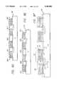
- FIG. 1is a cross-sectional view of a conventional EEPROM cell 110 taken along the line 1--1 in FIG. 3;
- FIG. 2is a schematic diagram of an array 104 of flash EEPROM cells 110 of FIG. 1 in a typical flash EEPROM 100;
- FIG. 3is an enlarged perspective view of a number of cells 110 within array 104 of FIG. 2.
- FIG. 4is a flowchart of the fabrication process shown in FIGS. 4A-4E;
- FIGS. 4A-4Eare sectional views of conventional cells 110 at various stages of fabrication
- FIG. 4Fis a graphical representation of net doping concentration with respect to junction depth for the source and drain regions for cell 110 of FIG. 1;
- FIG. 5is a sectional view of the circular region 800 shown in FIG. 4E;
- FIG. 6is a flowchart of the fabrication process shown in FIGS. 6A-6F;
- FIGS. 6A-6Fare sectional views of cells in accordance with a first embodiment of the present invention at various stages of fabrication including an intermediate n+ implant MDD1 performed after DDI and before the thermal cycle;
- FIG. 7is a graphical representation of net doping concentration with respect to junction depth for the source and drain regions for the cell of FIG. 6F;
- FIG. 8is a flowchart of the fabrication process shown in FIGS. 8A-8F;
- FIGS. 8A-8Fare sectional views of cells in accordance with a second embodiment of the present invention at various stages of fabrication including two steps for performing large angle n+ implants;
- FIG. 9is a graphical representation of net doping concentration with respect to junction depth for the source and drain regions for the cell of FIG. 8F.
- a pattern of field oxide regions 300, and stacked gate-word line structures 700are initially formed on a suitable substrate 116 (e.g., silicon implanted with p-type dopants, such as boron), then dopants are implanted in exposed regions of substrate 116 (in predetermined disposition to stacked gate structures 700) to form the source and drain regions of the respective cells 110 (Step 456).
- a suitable substrate 116e.g., silicon implanted with p-type dopants, such as boron
- Field oxide regions 300which provide electrical isolation of the various columns of cells, may be formed in any suitable manner (Step 448, FIG. 4).
- a field oxide layeris conventionally formed on substrate 116, then selectively removed (patterned) from above regions of the substrate where cells 110 are to be formed.
- the patterning processresults in alternating parallel strips of field oxide 300 and exposed regions corresponding to the columns of cells 110 in the array.
- Thismay be effected by, for example: growing a layer of thermal oxide ("barrier oxide” or "pad oxide”), over the surface of substrate 116; depositing a masking layer, frequently composed of nitride, on the barrier oxide over the core region; patterning the masking layer to overlie regions of the substrate where cells 110 are to be formed; growing the field oxide on the exposed areas of the barrier oxide by local oxidation of silicon, or LOCOS; stripping the masking layer to expose the underlying barrier oxide; and removing (e.g. etching) the exposed barrier oxide.
- thermal oxide"barrier oxide” or "pad oxide”
- masking layerfrequently composed of nitride
- stacked gate-word line structures 700function as: the tunnel dielectric 120; floating gate 122; interpoly dielectric 124; and control gate 126 of the respective cells 110 of array 104, integral to a common word line (WL) for the cells of each row in array 104.
- Stacked gate-word line structures 700may be formed in any suitable manner (Step 450).
- tunnel dielectric 120suitably comprising a thin (e.g. approximately 100 angstroms) layer of oxide, is initially formed on substrate 116 by any suitable technique, such as, for example, thermally oxidizing the surface of substrate 116 or by depositing a suitable material on substrate 116.
- a layer of suitable conductive polysilicon(e.g., polycrystalline silicon), that will ultimately form floating gates 122, is typically then formed on tunnel dielectric 120 layer.
- conductive polysiliconmay be deposited by any suitable technique, e.g., conventional chemical vapor deposition (CVD).
- CVDchemical vapor deposition
- the polysilicon layeris typically then masked and etched to remove strips overlying field oxide regions 300, leaving isolated strips of polysilicon on top of tunnel dielectric 120 overlying the substrate regions corresponding to the columns of cells 110 of array 104 (i.e. the regions in which source, channel, and drain regions of cells in the column will be formed).
- a layer of suitable dielectric materialsuch as, e.g., an oxide-nitrate-oxide (ONO) layer, that will ultimately form interpoly dielectric 124 is typically then formed by any suitable technique.
- ONOoxide-nitrate-oxide
- interpoly dielectric 124is suitably formed by growing a layer of oxide, depositing a layer of nitrate, followed by growing another layer of oxide.
- Interpoly dielectric 124 layer, in the completed arrayinsulates control gates 126 from floating gates 122 in the individual cells and fills the interstices between (and electrically isolates) the adjacent columns of floating gates 122 in array 104.
- conductive polysilicone.g., polycrystalline silicon
- control gates 126and word lines WL connecting the control gates of the cells in the respective rows of array 104
- CVDchemical vapor deposition
- tunnel dielectric layer 120portions of the respective polysilicon and interpoly dielectric layers are typically then selectively removed, to define stacked gate structures 700 on tunnel dielectric layer 120, i.e., to form the floating gates 122, interpoly dielectric layer 124 and control gates 126 of the individual cells, and word lines WL (portions of the interpoly dielectric and control gate polysilicon layers, bridging field oxide regions 300, to connect the respective cells of the rows of the array).
- Thisis typically effected by suitable masking and etching techniques.
- tunnel dielectric 120acts as a stop layer for this etch, resulting in removal of some or all of tunnel dielectric 120 overlying source 112 and drain 114 regions during the etch.
- tunnel dielectric 120 in the figuresdoes not overlie drain 114, which occurs when this portion of tunnel dielectric 120 is removed by the etching of the layers to form the stacked gate-word line structures 700.
- Step 452The portions of field oxide 300 and tunnel dielectric 120 between every second pair of adjacent word lines 700 in array 104 (i.e., the regions generally indicated as 302) are then typically removed (Step 452), in preparation for formation of the common line (CS, FIG. 2) connecting the sources.
- the source 112 of each cell in a column(excepting end cells) is formed in a common region with one of the adjacent cells, e.g., the preceding cell in the column.
- the drain of the cellis formed in a common region with the drain 114 of the other adjacent cell, e.g. , next succeeding cell in the column.
- the sources of each cell 110 in a roware formed as a common region, facilitating formation of common source line CS (FIG. 2).
- the drains of cells in adjacent rows at this point in the fabrication processremain electrically isolated by field oxide 300.
- a masking layer of photoresistis deposited over array 104, then patterned with regions 710 to mask the drain regions and field oxide regions between the drains of corresponding cells in adjacent rows, while exposing regions 302, i.e., the tunnel dielectric 120 overlying the portions of substrate 116 where source regions 112 are to be formed and the portions of field oxide 300 disposed between source regions 112 of the corresponding cells of adjacent columns (Step 453).
- the edges of each opening of the maskare typically aligned to rest on the word lines of adjacent rows of cells, covering drain regions 112 and the field oxide regions isolating the drains of cells in adjacent columns.
- a highly selective etche.g., a conventional Self-Aligned Source (SAS) etch
- SASSelf-Aligned Source
- a conventional SAS etchis described in U.S. Pat. No. 5,120,671, issued Jun. 9, 1992, to Tang et al. When completed, this etch creates the structure shown in FIG. 4A.
- the selective etchtypically removes not only the exposed field oxide regions 300, but also the exposed tunnel oxide 120, and a portion of the underlying substrate 116.
- Source 112 and drain 114 regionsare then formed (Step 456).
- source regions 112are conventionally formed by initially implanting n-type dopants with a conventional double diffusion implant (DDI) while retaining mask 710 (Step 458).
- the DDIimplants a first dopant, suitably phosphorous, to form a deeply diffused but lightly doped N well 130 (FIGS. 1 and 4B), establishing a graded source-channel junction.
- the photoresist comprising mask 710is then removed (Step 460).
- the DDI implantis typically driven deeper into substrate 116, as shown in FIG. 4C, by subjecting substrate 116 to a thermal cycle at high temperature (e.g. 1050 degrees Fahrenheit)(Step 462).
- a shallow second implantis then performed (e.g., with arsenic) (Step 464) to create a more heavily doped, but shallower, n+ well 132 embedded within deep N well 130 (FIG. 4D).
- the MDD implantalso forms a shallow, abrupt drain 114. This implantation process tends to result in a cell manifesting source and drain doping profiles (relative to the source-channel and drain-channel junctions respectively) shown in FIG. 4F.
- Step 466The entire device is then oxidized (Step 466) to form a sealing layer 720 of silicon dioxide (FIG. 4E).
- the EEPROM 100is then conventionally finished and packaged for distribution.
- the disparity of erase times in conventional EEPROM cells 110 within array 104is caused, at least in part, by structural and doping variations among cells 110.
- the erase time of cell 110is affected by the F-N tunneling rate through tunnel dielectric 120, which, in turn, varies inversely with the square of the distance between floating gate 122 and source 112 in tunneling region 140.
- the geometry of each cell 110 near tunneling region 140is difficult to control without significantly increasing the size of each cell.
- the final oxidation (layer 720, step 460) of EEPROM 100typically deforms floating gate 122, causing a rounding 123 of floating gate 122 in tunneling region 140.
- the shape and extent of the rounding 123affects the distance across tunnel dielectric 120, and thus the erase time of each cell 110. Because the rounding effect is different among various cells 110 in array 104, erase times among cells 110 likewise vary.
- F-N tunnelingis affected by the doping concentration of tunneling region 140 near source 112, specifically at the surface of channel 118; higher density doping at the surface tends to provide higher rates of F-N tunneling.
- the higher doping densityresults in less voltage drop in the silicon, which provides for more voltage across tunnel dielectric 120, thereby enhancing the F-N tunneling rate.
- the differences in cell 110 geometriesnot only affect the distance between floating gate 122 and source 112, but may also affect the doping concentration of source 112 in tunneling region 140 in each cell.
- a highly selective etche.g., a conventional Self-Aligned Source (SAS) etch
- SASSelf-Aligned Source
- This etchis selective in that it etches the field oxide at a much higher rate than the polysilicon word line.
- tunnel dielectric 120 overlying the portions of substrate 116 where source regions 112 are to be formedis also subject to the etch, and the etch operates upon tunnel oxide 120 at the same rate as field oxide 300.
- Field oxide 300is typically considerably thicker (e.g., 3000 Angstroms) than tunnel oxide 120 (e.g., 100 Angstroms).
- the selective etchtypically removes a portion of substrate 116, producing a gouge of depth D G in upper surface 113 of source region source 112.
- the depth D G of the gouge in source region 112 and the profile of surface 113significantly affect the diffusion of dopants into tunneling region 140.
- the gougeincreases the distance through which the dopants must travel to extend to the surface of channel 118. Consequently, the gouge in surface 113 tends to decrease doping concentration in source 112 in tunneling region 140 when compared to an ungouged surface.
- erase timesare improved (and hence, leakage current is reduced) by improving the doping profile in tunneling region 140 of substrate 116, i.e. moving the dopants farther under floating gate 122.
- the n+ portion 132 of source region 112underlies floating gate 122 by a greater extent than does the n+ drain region 114.
- the ratio of the doping profile of n+ dopant (e.g. arsenic) in source region 112 in a predetermined portion of the tunneling region 140 to the doping profile of n+ dopant in the corresponding portion of drain region 114is suitably in the range of 1.1 to 10, preferably in the range of 1.2 to 5, and most preferably in the range of 1.5 to 3.
- an EEPROM 101 with improved column leakage current characteristicshas cells 106 fabricated using an intermediate n+ implant in source 112 to increase the doping concentration in tunneling region 140.
- An intermediate n+ implant MDD1may suitably be added immediately following the DDI implant (FIG. 6B) and preceding the thermal cycle (FIG. 6D).
- the initial steps of the fabrication processsuch as forming field oxide regions 300 (Step 448) and gate structures 700 (Step 450), effecting the mask 710 and selective etch to selectively remove source tunnel dielectric 120 and field oxide 300 (Step 452), and the initial DDI (Step 458), may be effected in any suitable manner, for example, as previously described in relation to FIGS.
- MDD1Prior to the thermal cycle to drive the DDI implant deeper, however, intermediate n+ implant MDD1 adds further dopants (e.g. arsenic) (step 670, FIG. 6G) to source 112 (FIG. 6C).
- MDD1provides a first predetermined dose of dopant, suitably less (e.g. 80%) than conventional MDD doses (e.g. 6 ⁇ 10 15 /cm 2 ), such as the full MDD dose of FIG. 4D.
- the dose of MDD1may vary from a small percentage of a conventional MDD dose all the way up to the full MDD dose (or more). However, the higher the dose of MDD1, the deeper the junction will be driven during the subsequent thermal cycle.
- the first predetermined dose of dopant provided by MDD1is in the range of 1 ⁇ 10 3 /cm 2 to 15 ⁇ 10 15 /cm 2 , and preferably, in the range of 5 ⁇ 10 14/cm 2 to 7 ⁇ 10 15 /cm 2 , and most preferably, in the range of 1 ⁇ 10 15 /cm 2 to 5 ⁇ 10 15 /cm 2 .
- mask 710is suitably removed, and the DDI and intermediate n+ implant are suitably driven deeper into substrate 116 with the thermal cycle described above.
- MDD1immediately after the DDI implant allows mask 710 to be used for the MDD1 implant as well as for the DDI implant.
- MDD1only requires the addition of one process step, namely, the implantation step. No additional masking or etching steps are required, making the addition of MDD1 into the standard process flow of the prior art very efficient and cost-effective.
- a second n+ implant MDD2is suitably provided (step 672) to implant a second predetermined dose of n+ dopants (FIG. 6E).
- the second predetermined dose of dopant provided by MDD2is in the range of 1 ⁇ 10 14 /cm 2 to 15 ⁇ 10 15 /cm 2 , and preferably, in the range of 5 ⁇ 10 14 /cm 2 to 10 ⁇ 10 15 /cm 2 , and most preferably, in the range of 2 ⁇ 10 15 /cm 2 to 6 ⁇ 10 15 /cm 2 .
- the dose provided by MDD2is suitably the full dose provided by a conventional MDD.
- the dosage of MDD2may be reduced by the amount of the intermediate n+ implant MDD1 already performed.
- Providing intermediate n+ implant MDD1 with a full n+ implant dose MDD2suitably further enhances the doping concentration in tunneling region 140.
- oxide layer 720may be grown over the array (step 460), as shown in FIG. 6F. The process of FIGS. 6 and 6A-6F tends to result in a cell 106 manifesting source and drain doping profiles (relative to the source-channel and drain-channel junctions respectively) shown in FIG. 7.
- Performing a thermal cycle (step 456) following the intermediate n+ implant (step 670)tends to drive a higher concentration of n+ dopant into tunneling region 140 of source 112 (i.e. the portion of source region 112 overlapped by floating gate 122). This not only enhances the uniformity of erase times among cells 106 in array 104, but, additionally, increases the rate of F-N tunneling, and thus provides a faster erase time while maintaining the same cell size.
- the doping concentration in tunneling region 140depends on how deeply the implants (e.g. DDI, MDD1 and MDD2) are driven into substrate 116. Referring to FIG. 5, the doping concentration at the junction of deep well 130 and substrate 116 is light, and is typically heaviest near the upper surface of source 112. Thus, based on doping concentration, F-N tunneling is more likely to occur in region B-C than in region A-B.
- n+ dopants deeper into substrate 116also reduces the effects of gouging in source region 112. Since the n+ dopants diffuse more freely during the thermal drive, a higher concentration of n+ dopants is created near the surface of channel 118 in tunneling region 140. In addition, driving the n+ dopants deeper into substrate 116 reduces the effects of rounding 123 of floating gate 122, since higher concentrations of n+ dopants are driven past rounding 123. Thus, the intermediate n+ implant MDD1 and subsequent thermal drive tend to compensate for variations in the geometry (i.e. gouging of source region and rounding of floating gate 122) in runnel region 140 to provide greater tunneling rate uniformity (and hence, erase time,uniformity). More uniform erase time in cells 106 decreases the column leakage current in array 104.
- the n+ implant for source region 112may be performed at an angle to increase uniformity of erase time.
- the initial steps of the fabrication processsuch as forming field oxide regions 300 (Step 448) and gate structures 700 (Step 450), effecting mask 710 and the selective etch (e.g. SAS etch) to selectively remove field oxide 300 (Step 452), and the initial DDI (Step 458), may be effected in any suitable manner, for example, as previously described in relation to FIGS. 3 and 4A-4B.
- a thermal cyclestep 456 (FIG.
- n+ implant 8Cis effected after the initial DDI, suitably as described in conjunction with FIG. 4C.
- the n+ implantis suitably effected at an angle, for each source channel junction.
- a predetermined percentagee.g., 10% to 100%, and preferably half
- the full n+ dose MDD1is implanted at a relatively large positive angle (e.g. suitably +7 to +50 degrees, and preferably, +20 to +40 degrees, and most preferably approximately +30 degrees) relative to perpendicular (step 880).
- a relatively large positive anglee.g. suitably +7 to +50 degrees, and preferably, +20 to +40 degrees, and most preferably approximately +30 degrees
- the other half of the n+ dose MDD2is implanted at a negative angle (step 882) corresponding to the relatively large angle used in the first step (e.g., most preferably approximately -30 degrees).
- oxide 720may be grown over the entire structure (step 460), as shown in FIG. 8F.
- implanting the n+ dopant at an anglereduces the undesirable effect of the gouging in source region 112 caused by the highly selective, e.g. SAS, etch (step 452).
- a greater proportion of the doseis available at the portion of source 112 closest to floating gate 122, causing the n+ dopant to be diffused under floating gate 122.
- Thistends to increase the doping concentration in tunneling region 140, which correspondingly tends to decrease erase time for slower memory cells 106.
- the range of erase times among cells 110 in array 104may diminish, resulting in a smaller column leakage current.
- the doping concentration (generally indicated as 900) for the angled n+ implant at the edge (0.0, in FIG. 9) of floating gate 122is slightly less than the doping concentration (902) for the traditional n+ implant (e.g. from the edge (0.0) of floating gate 122 to approximately 0.05 microns under the floating gate).
- the doping concentration 900 for the angled n+ implantis greater than the doping concentration 902 for the traditional n+ implant in the region (910) extending from approximately 0.05 to 0.15 microns under floating gate 122 (FIG. 9).
- This higher doping concentration farther under floating gate 122results in a faster erase time for an individual cell 106, and a more uniform erase time across the cells within the array.
- tunneling region 140counteracts the negative effects of varying geometry among cells 106.
- each cell 106has more uniform doping characteristics, providing enhanced uniformity of erase times.
- the enhanced uniformityreduces the likelihood of any cell being over-erased, thus reducing the susceptibility to column leakage current. Consequently, the endurance and reliability of EEPROM 101 may be improved.
- an angled n+ implantcould also be used to form the source region with a separate, traditional n+ implant used to form the drain region.
- the process shown in FIGS. 6A-6Fcould be modified so that the MDD1 implant is effected as an n+ implant performed in two steps, the first at a positive angle and the second at a negative angle.
- the subsequent n+ implant(FIG. 6E) would then form the drain regions, and could either augment the n+ concentration in the source regions, or leave the source regions unaffected.
- step 454the process described shows the formation of a double-diffused source (step 454)
- the method in accordance with the present inventionalso applies to abrupt source junctions without deep well 130.
- source 112is described herein as double-diffused, assuming cells 106 are erased from the source side, the present invention applies with equal force to cells 106 that are erased from the drain side, with either a single or double diffused drain region.
- thermal cycle of the method in accordance with the present inventionis described as suitably identical to the prior art thermal cycle, but it is understood that the thermal cycle in accordance with the present invention may be modified as needed to optimize the diffusion of n+ dopants into substrate 116 underlying floating gate 122.
Landscapes
- Non-Volatile Memory (AREA)
- Semiconductor Memories (AREA)
Abstract
Description
Claims (23)
Priority Applications (2)
| Application Number | Priority Date | Filing Date | Title |
|---|---|---|---|
| US08/403,460US5482881A (en) | 1995-03-14 | 1995-03-14 | Method of making flash EEPROM memory with reduced column leakage current |
| US08/684,920US5652447A (en) | 1995-03-14 | 1996-07-22 | Flash EEPROM memory with reduced column leakage current |
Applications Claiming Priority (1)
| Application Number | Priority Date | Filing Date | Title |
|---|---|---|---|
| US08/403,460US5482881A (en) | 1995-03-14 | 1995-03-14 | Method of making flash EEPROM memory with reduced column leakage current |
Related Child Applications (1)
| Application Number | Title | Priority Date | Filing Date |
|---|---|---|---|
| US46506995ADivision | 1995-03-14 | 1995-06-05 |
Publications (1)
| Publication Number | Publication Date |
|---|---|
| US5482881Atrue US5482881A (en) | 1996-01-09 |
Family
ID=23595866
Family Applications (2)
| Application Number | Title | Priority Date | Filing Date |
|---|---|---|---|
| US08/403,460Expired - LifetimeUS5482881A (en) | 1995-03-14 | 1995-03-14 | Method of making flash EEPROM memory with reduced column leakage current |
| US08/684,920Expired - LifetimeUS5652447A (en) | 1995-03-14 | 1996-07-22 | Flash EEPROM memory with reduced column leakage current |
Family Applications After (1)
| Application Number | Title | Priority Date | Filing Date |
|---|---|---|---|
| US08/684,920Expired - LifetimeUS5652447A (en) | 1995-03-14 | 1996-07-22 | Flash EEPROM memory with reduced column leakage current |
Country Status (1)
| Country | Link |
|---|---|
| US (2) | US5482881A (en) |
Cited By (26)
| Publication number | Priority date | Publication date | Assignee | Title |
|---|---|---|---|---|
| US5656513A (en)* | 1995-06-07 | 1997-08-12 | Advanced Micro Devices, Inc. | Nonvolatile memory cell formed using self aligned source implant |
| US5708588A (en)* | 1995-04-07 | 1998-01-13 | Advanced Micro Devices, Inc. | Flash EEPROM memory with improved discharged speed using substrate bias and method therefor |
| US5796670A (en)* | 1996-11-07 | 1998-08-18 | Ramax Semiconductor, Inc. | Nonvolatile dynamic random access memory device |
| US5854108A (en)* | 1996-06-04 | 1998-12-29 | Advanced Micro Devices, Inc. | Method and system for providing a double diffuse implant junction in a flash device |
| US5856223A (en)* | 1997-02-25 | 1999-01-05 | Winbond Electronics Corp. | Method for manufacturing self-aligned split-gate flash memory cells |
| US5972749A (en)* | 1998-01-05 | 1999-10-26 | Advanced Micro Devices, Inc. | Method for preventing P1 punchthrough |
| US6057191A (en)* | 1996-06-26 | 2000-05-02 | Sgs-Thomson Microelectronics S.R.L. | Process for the fabrication of integrated circuits with contacts self-aligned to active areas |
| US6130134A (en)* | 1997-03-05 | 2000-10-10 | Macronix International Co., Ltd. | Method for forming asymmetric flash EEPROM with a pocket to focus electron injections |
| US6297098B1 (en)* | 1999-11-01 | 2001-10-02 | Taiwan Semiconductor Manufacturing Company | Tilt-angle ion implant to improve junction breakdown in flash memory application |
| US6329257B1 (en)* | 1997-12-19 | 2001-12-11 | Advanced Micro Devices, Inc. | Method for laterally peaked source doping profiles for better erase control in flash memory devices |
| US6579781B1 (en)* | 2000-07-19 | 2003-06-17 | Advanced Micro Devices, Inc. | Elimination of n+ contact implant from flash technologies by replacement with standard double-diffused and n+ implants |
| US6680257B2 (en)* | 2001-07-30 | 2004-01-20 | Eon Silicon Devices, Inc. | Alternative related to SAS in flash EEPROM |
| US20040014282A1 (en)* | 2002-07-17 | 2004-01-22 | Kouichi Shimoda | Method for manufacturing nonvolatile semiconductor memory device |
| US20040082127A1 (en)* | 1999-10-05 | 2004-04-29 | Advanced Micro Devices, Inc. | Method and system for reducing short channel effects in a memory device by reduction of drain thermal cycling |
| US6737344B2 (en)* | 2000-11-28 | 2004-05-18 | Sharp Kabushiki Kaisha | Method for manufacturing nonvolatile semiconductor memory with narrow variation in threshold voltages of memory cells |
| US6800891B2 (en) | 2001-02-02 | 2004-10-05 | Micron Technology, Inc. | Self-aligned source pocket for flash memory cells |
| US6810296B2 (en)* | 2002-09-25 | 2004-10-26 | Advanced Micro Devices, Inc. | Correlating an inline parameter to a device operation parameter |
| US6812531B1 (en) | 1998-05-11 | 2004-11-02 | Stmicroelectronics S.R.L. | Matrix of memory cells fabricated by means of a self-aligned source process, comprising ROM memory cells, and related manufacturing process |
| US20050074925A1 (en)* | 2003-10-01 | 2005-04-07 | Kim Jum Soo | Method for fabricating a semiconductor device |
| US6906376B1 (en)* | 2002-06-13 | 2005-06-14 | A Plus Flash Technology, Inc. | EEPROM cell structure and array architecture |
| KR100503365B1 (en)* | 2003-10-01 | 2005-07-26 | 동부아남반도체 주식회사 | Fabrication method of semiconductor device |
| US20070087502A1 (en)* | 2005-10-13 | 2007-04-19 | Chen Chung-Zen | Method of forming FLASH cell array having reduced word line pitch |
| US20110133264A1 (en)* | 2009-12-04 | 2011-06-09 | Semiconductor Manufacturing International (Shanghai) Corporation | System and method for eeprom architecture |
| US20120099381A1 (en)* | 2010-06-04 | 2012-04-26 | Peking University | Embedded non-volatile memory cell, operation method and memory array thereof |
| US20150221752A1 (en)* | 2012-07-12 | 2015-08-06 | Taiwan Semiconductor Manufacturing Company, Ltd. | Apparatus and Method for Memory Device |
| US20150364558A1 (en)* | 2014-06-17 | 2015-12-17 | Taiwan Semiconductor Manufacturing Co., Ltd. | Split gate flash memory structure and method of making the split gate flash memory structure |
Families Citing this family (15)
| Publication number | Priority date | Publication date | Assignee | Title |
|---|---|---|---|---|
| US5801076A (en)* | 1995-02-21 | 1998-09-01 | Advanced Micro Devices, Inc. | Method of making non-volatile memory device having a floating gate with enhanced charge retention |
| US5714412A (en)* | 1996-12-02 | 1998-02-03 | Taiwan Semiconductor Manufacturing Company, Ltd | Multi-level, split-gate, flash memory cell and method of manufacture thereof |
| US6127224A (en)* | 1997-12-31 | 2000-10-03 | Stmicroelectronics, S.R.L. | Process for forming a non-volatile memory cell with silicided contacts |
| JPH11265947A (en)* | 1998-03-17 | 1999-09-28 | Fujitsu Ltd | Semiconductor device and manufacturing method thereof |
| US7192829B2 (en)* | 1998-07-17 | 2007-03-20 | Micron Technology, Inc. | Methods of forming floating gate transistors |
| TW400609B (en)* | 1998-08-04 | 2000-08-01 | United Microelectronics Corp | The structure of flash memory and its manufacturing method |
| US6046932A (en)* | 1999-08-13 | 2000-04-04 | Advanced Micro Devices, Inc. | Circuit implementation to quench bit line leakage current in programming and over-erase correction modes in flash EEPROM |
| US6329273B1 (en)* | 1999-10-29 | 2001-12-11 | Advanced Micro Devices, Inc. | Solid-source doping for source/drain to eliminate implant damage |
| US6208559B1 (en) | 1999-11-15 | 2001-03-27 | Lattice Semiconductor Corporation | Method of operating EEPROM memory cells having transistors with thin gate oxide and reduced disturb |
| US6549466B1 (en)* | 2000-02-24 | 2003-04-15 | Advanced Micro Devices, Inc. | Using a negative gate erase voltage applied in steps of decreasing amounts to reduce erase time for a non-volatile memory cell with an oxide-nitride-oxide (ONO) structure |
| US6284603B1 (en)* | 2000-07-12 | 2001-09-04 | Chartered Semiconductor Manufacturing Inc. | Flash memory cell structure with improved channel punch-through characteristics |
| JP2004063527A (en)* | 2002-07-25 | 2004-02-26 | Elpida Memory Inc | Semiconductor storage device and method of manufacturing the same |
| US7078761B2 (en)* | 2004-03-05 | 2006-07-18 | Chingis Technology Corporation | Nonvolatile memory solution using single-poly pFlash technology |
| US7388251B2 (en)* | 2004-08-11 | 2008-06-17 | Micron Technology, Inc. | Non-planar flash memory array with shielded floating gates on silicon mesas |
| KR100829604B1 (en)* | 2006-09-26 | 2008-05-14 | 삼성전자주식회사 | Nonvolatile Memory Device and Manufacturing Method Thereof |
Citations (5)
| Publication number | Priority date | Publication date | Assignee | Title |
|---|---|---|---|---|
| US4698787A (en)* | 1984-11-21 | 1987-10-06 | Exel Microelectronics, Inc. | Single transistor electrically programmable memory device and method |
| US5100818A (en)* | 1988-08-26 | 1992-03-31 | Mitsubishi Denki Kabushiki Kaisha | Non-volatile semiconductor memory device and method of manufacturing the same |
| US5120671A (en)* | 1990-11-29 | 1992-06-09 | Intel Corporation | Process for self aligning a source region with a field oxide region and a polysilicon gate |
| US5335198A (en)* | 1993-05-06 | 1994-08-02 | Advanced Micro Devices, Inc. | Flash EEPROM array with high endurance |
| US5364806A (en)* | 1991-08-29 | 1994-11-15 | Hyundai Electronics Industries Co., Ltd. | Method of making a self-aligned dual-bit split gate (DSG) flash EEPROM cell |
Family Cites Families (5)
| Publication number | Priority date | Publication date | Assignee | Title |
|---|---|---|---|---|
| JP2500871B2 (en)* | 1991-03-30 | 1996-05-29 | 株式会社東芝 | Semiconductor non-volatile RAM |
| US5317179A (en)* | 1991-09-23 | 1994-05-31 | Integrated Silicon Solution, Inc. | Non-volatile semiconductor memory cell |
| JPH0677492A (en)* | 1992-07-22 | 1994-03-18 | Rohm Co Ltd | Semiconductor device having nonvolatile memory circuit and method of manufacturing the same |
| JP3584338B2 (en)* | 1994-03-03 | 2004-11-04 | ローム・ユーエスエー・インク | Method for erasing electrically erasable and programmable devices |
| US5413946A (en)* | 1994-09-12 | 1995-05-09 | United Microelectronics Corporation | Method of making flash memory cell with self-aligned tunnel dielectric area |
- 1995
- 1995-03-14USUS08/403,460patent/US5482881A/ennot_activeExpired - Lifetime
- 1996
- 1996-07-22USUS08/684,920patent/US5652447A/ennot_activeExpired - Lifetime
Patent Citations (5)
| Publication number | Priority date | Publication date | Assignee | Title |
|---|---|---|---|---|
| US4698787A (en)* | 1984-11-21 | 1987-10-06 | Exel Microelectronics, Inc. | Single transistor electrically programmable memory device and method |
| US5100818A (en)* | 1988-08-26 | 1992-03-31 | Mitsubishi Denki Kabushiki Kaisha | Non-volatile semiconductor memory device and method of manufacturing the same |
| US5120671A (en)* | 1990-11-29 | 1992-06-09 | Intel Corporation | Process for self aligning a source region with a field oxide region and a polysilicon gate |
| US5364806A (en)* | 1991-08-29 | 1994-11-15 | Hyundai Electronics Industries Co., Ltd. | Method of making a self-aligned dual-bit split gate (DSG) flash EEPROM cell |
| US5335198A (en)* | 1993-05-06 | 1994-08-02 | Advanced Micro Devices, Inc. | Flash EEPROM array with high endurance |
Cited By (37)
| Publication number | Priority date | Publication date | Assignee | Title |
|---|---|---|---|---|
| US5708588A (en)* | 1995-04-07 | 1998-01-13 | Advanced Micro Devices, Inc. | Flash EEPROM memory with improved discharged speed using substrate bias and method therefor |
| US5656513A (en)* | 1995-06-07 | 1997-08-12 | Advanced Micro Devices, Inc. | Nonvolatile memory cell formed using self aligned source implant |
| US5854108A (en)* | 1996-06-04 | 1998-12-29 | Advanced Micro Devices, Inc. | Method and system for providing a double diffuse implant junction in a flash device |
| US6057191A (en)* | 1996-06-26 | 2000-05-02 | Sgs-Thomson Microelectronics S.R.L. | Process for the fabrication of integrated circuits with contacts self-aligned to active areas |
| US5796670A (en)* | 1996-11-07 | 1998-08-18 | Ramax Semiconductor, Inc. | Nonvolatile dynamic random access memory device |
| US5856223A (en)* | 1997-02-25 | 1999-01-05 | Winbond Electronics Corp. | Method for manufacturing self-aligned split-gate flash memory cells |
| US6130134A (en)* | 1997-03-05 | 2000-10-10 | Macronix International Co., Ltd. | Method for forming asymmetric flash EEPROM with a pocket to focus electron injections |
| US6329257B1 (en)* | 1997-12-19 | 2001-12-11 | Advanced Micro Devices, Inc. | Method for laterally peaked source doping profiles for better erase control in flash memory devices |
| US5972749A (en)* | 1998-01-05 | 1999-10-26 | Advanced Micro Devices, Inc. | Method for preventing P1 punchthrough |
| US6066873A (en)* | 1998-01-05 | 2000-05-23 | Advanced Micro Devices, Inc. | Method and apparatus for preventing P1 punchthrough |
| US6812531B1 (en) | 1998-05-11 | 2004-11-02 | Stmicroelectronics S.R.L. | Matrix of memory cells fabricated by means of a self-aligned source process, comprising ROM memory cells, and related manufacturing process |
| US20040082127A1 (en)* | 1999-10-05 | 2004-04-29 | Advanced Micro Devices, Inc. | Method and system for reducing short channel effects in a memory device by reduction of drain thermal cycling |
| US6297098B1 (en)* | 1999-11-01 | 2001-10-02 | Taiwan Semiconductor Manufacturing Company | Tilt-angle ion implant to improve junction breakdown in flash memory application |
| US20020019103A1 (en)* | 1999-11-01 | 2002-02-14 | Taiwan Semiconductor Manufacturing Company | Tilt-angle ion implant to improve junction breakdown in flash memory application |
| US6579781B1 (en)* | 2000-07-19 | 2003-06-17 | Advanced Micro Devices, Inc. | Elimination of n+ contact implant from flash technologies by replacement with standard double-diffused and n+ implants |
| US20040183120A1 (en)* | 2000-11-28 | 2004-09-23 | Sharp Kabushiki Kaisha | Method for manufacturing nonvolatile semiconductor memory with narrow variation in threshold voltages of memory cells |
| US6737344B2 (en)* | 2000-11-28 | 2004-05-18 | Sharp Kabushiki Kaisha | Method for manufacturing nonvolatile semiconductor memory with narrow variation in threshold voltages of memory cells |
| US6800891B2 (en) | 2001-02-02 | 2004-10-05 | Micron Technology, Inc. | Self-aligned source pocket for flash memory cells |
| US6806143B2 (en)* | 2001-02-02 | 2004-10-19 | Micron Technology, Inc. | Self-aligned source pocket for flash memory cells |
| US6864523B2 (en) | 2001-02-02 | 2005-03-08 | Micron Technology, Inc. | Self-aligned source pocket for flash memory cells |
| US6680257B2 (en)* | 2001-07-30 | 2004-01-20 | Eon Silicon Devices, Inc. | Alternative related to SAS in flash EEPROM |
| US6906376B1 (en)* | 2002-06-13 | 2005-06-14 | A Plus Flash Technology, Inc. | EEPROM cell structure and array architecture |
| US6756269B2 (en)* | 2002-07-17 | 2004-06-29 | Oki Electric Industry Co., Ltd. | Method for manufacturing nonvolatile semiconductor memory device |
| US20040014282A1 (en)* | 2002-07-17 | 2004-01-22 | Kouichi Shimoda | Method for manufacturing nonvolatile semiconductor memory device |
| US6810296B2 (en)* | 2002-09-25 | 2004-10-26 | Advanced Micro Devices, Inc. | Correlating an inline parameter to a device operation parameter |
| KR100503365B1 (en)* | 2003-10-01 | 2005-07-26 | 동부아남반도체 주식회사 | Fabrication method of semiconductor device |
| US20050074925A1 (en)* | 2003-10-01 | 2005-04-07 | Kim Jum Soo | Method for fabricating a semiconductor device |
| US7074682B2 (en)* | 2003-10-01 | 2006-07-11 | Dongbuanam Semiconductor Inc. | Method for fabricating a semiconductor device having self aligned source (SAS) crossing trench |
| US20070087502A1 (en)* | 2005-10-13 | 2007-04-19 | Chen Chung-Zen | Method of forming FLASH cell array having reduced word line pitch |
| US7271063B2 (en)* | 2005-10-13 | 2007-09-18 | Elite Semiconductor Memory Technology, Inc. | Method of forming FLASH cell array having reduced word line pitch |
| US20110133264A1 (en)* | 2009-12-04 | 2011-06-09 | Semiconductor Manufacturing International (Shanghai) Corporation | System and method for eeprom architecture |
| US8470669B2 (en)* | 2009-12-04 | 2013-06-25 | Semiconductor Manufacturing International (Shanghai) Corporation | System and method for EEPROM architecture |
| US20120099381A1 (en)* | 2010-06-04 | 2012-04-26 | Peking University | Embedded non-volatile memory cell, operation method and memory array thereof |
| US20150221752A1 (en)* | 2012-07-12 | 2015-08-06 | Taiwan Semiconductor Manufacturing Company, Ltd. | Apparatus and Method for Memory Device |
| US10164073B2 (en)* | 2012-07-12 | 2018-12-25 | Taiwan Semiconductor Manufacturing Company, Ltd. | Apparatus and method for memory device |
| US20150364558A1 (en)* | 2014-06-17 | 2015-12-17 | Taiwan Semiconductor Manufacturing Co., Ltd. | Split gate flash memory structure and method of making the split gate flash memory structure |
| US9614048B2 (en)* | 2014-06-17 | 2017-04-04 | Taiwan Semiconductor Manufacturing Co., Ltd. | Split gate flash memory structure and method of making the split gate flash memory structure |
Also Published As
| Publication number | Publication date |
|---|---|
| US5652447A (en) | 1997-07-29 |
Similar Documents
| Publication | Publication Date | Title |
|---|---|---|
| US5482881A (en) | Method of making flash EEPROM memory with reduced column leakage current | |
| US5656513A (en) | Nonvolatile memory cell formed using self aligned source implant | |
| US5284785A (en) | Diffusionless source/drain conductor electrically-erasable, electrically-programmable read-only memory and methods for making and using the same | |
| US6914817B2 (en) | Highly compact EPROM and flash EEPROM devices | |
| US5471422A (en) | EEPROM cell with isolation transistor and methods for making and operating the same | |
| US5242848A (en) | Self-aligned method of making a split gate single transistor non-volatile electrically alterable semiconductor memory device | |
| US5278087A (en) | Method of making a single transistor non-volatile electrically alterable semiconductor memory device with a re-crystallized floating gate | |
| US5045488A (en) | Method of manufacturing a single transistor non-volatile, electrically alterable semiconductor memory device | |
| US5029130A (en) | Single transistor non-valatile electrically alterable semiconductor memory device | |
| US5572054A (en) | Method of operating a single transistor non-volatile electrically alterable semiconductor memory device | |
| US5067108A (en) | Single transistor non-volatile electrically alterable semiconductor memory device with a re-crystallized floating gate | |
| US5753952A (en) | Nonvolatile memory cell with P-N junction formed in polysilicon floating gate | |
| US5371031A (en) | Method of making EEPROM array with buried N+ windows and with separate erasing and programming regions | |
| JPH07221209A (en) | Flash EEPROM cell with gap between floating gate and drain for high hot electron injection efficiency for programming | |
| EP0579779B1 (en) | A single transistor non-volatile electrically alterable semiconductor memory device | |
| WO1994014196A1 (en) | High density contactless flash eprom array using channel erase | |
| US6313498B1 (en) | Flash memory cell with thin floating gate with rounded side wall, and fabrication process | |
| US5045491A (en) | Method of making a nonvolatile memory array having cells with separate program and erase regions | |
| US5354703A (en) | EEPROM cell array with tight erase distribution | |
| US5523249A (en) | Method of making an EEPROM cell with separate erasing and programming regions | |
| US6251717B1 (en) | Viable memory cell formed using rapid thermal annealing | |
| KR20000013791A (en) | Flash non-volatile semiconductor memory device for preventing an over-erase | |
| US5147816A (en) | Method of making nonvolatile memory array having cells with two tunelling windows | |
| KR100243493B1 (en) | Asymmetric Nonvolatile Memory Cells, Arrays and Manufacturing Methods Thereof | |
| US5032533A (en) | Method of making a nonvolatile memory cell with field-plate switch |
Legal Events
| Date | Code | Title | Description |
|---|---|---|---|
| AS | Assignment | Owner name:ADVANCED MICRO DEVICES, INC.I, CALIFORNIA Free format text:ASSIGNMENT OF ASSIGNORS INTEREST;ASSIGNORS:CHEN, JIAN;TANG, YUAN;LUNING, SCOTT;AND OTHERS;REEL/FRAME:007393/0390;SIGNING DATES FROM 19950306 TO 19950308 | |
| STCF | Information on status: patent grant | Free format text:PATENTED CASE | |
| CC | Certificate of correction | ||
| FPAY | Fee payment | Year of fee payment:4 | |
| FPAY | Fee payment | Year of fee payment:8 | |
| AS | Assignment | Owner name:SPANSION INC., CALIFORNIA Free format text:ASSIGNMENT OF ASSIGNORS INTEREST;ASSIGNOR:ADVANCED MICRO DEVICES, INC.;REEL/FRAME:019028/0599 Effective date:20070131 | |
| AS | Assignment | Owner name:SPANSION LLC, CALIFORNIA Free format text:ASSIGNMENT OF ASSIGNORS INTEREST;ASSIGNOR:SPANSION INC.;REEL/FRAME:019063/0771 Effective date:20070131 | |
| FPAY | Fee payment | Year of fee payment:12 | |
| AS | Assignment | Owner name:BARCLAYS BANK PLC,NEW YORK Free format text:SECURITY AGREEMENT;ASSIGNORS:SPANSION LLC;SPANSION INC.;SPANSION TECHNOLOGY INC.;AND OTHERS;REEL/FRAME:024522/0338 Effective date:20100510 Owner name:BARCLAYS BANK PLC, NEW YORK Free format text:SECURITY AGREEMENT;ASSIGNORS:SPANSION LLC;SPANSION INC.;SPANSION TECHNOLOGY INC.;AND OTHERS;REEL/FRAME:024522/0338 Effective date:20100510 | |
| AS | Assignment | Owner name:SPANSION INC., CALIFORNIA Free format text:RELEASE BY SECURED PARTY;ASSIGNOR:BARCLAYS BANK PLC;REEL/FRAME:035201/0159 Effective date:20150312 Owner name:SPANSION LLC, CALIFORNIA Free format text:RELEASE BY SECURED PARTY;ASSIGNOR:BARCLAYS BANK PLC;REEL/FRAME:035201/0159 Effective date:20150312 Owner name:SPANSION TECHNOLOGY LLC, CALIFORNIA Free format text:RELEASE BY SECURED PARTY;ASSIGNOR:BARCLAYS BANK PLC;REEL/FRAME:035201/0159 Effective date:20150312 | |
| AS | Assignment | Owner name:MORGAN STANLEY SENIOR FUNDING, INC., NEW YORK Free format text:SECURITY INTEREST;ASSIGNORS:CYPRESS SEMICONDUCTOR CORPORATION;SPANSION LLC;REEL/FRAME:035240/0429 Effective date:20150312 | |
| AS | Assignment | Owner name:CYPRESS SEMICONDUCTOR CORPORATION, CALIFORNIA Free format text:ASSIGNMENT OF ASSIGNORS INTEREST;ASSIGNOR:SPANSION, LLC;REEL/FRAME:036021/0118 Effective date:20150601 | |
| AS | Assignment | Owner name:CYPRESS SEMICONDUCTOR CORPORATION, CALIFORNIA Free format text:PARTIAL RELEASE OF SECURITY INTEREST IN PATENTS;ASSIGNOR:MORGAN STANLEY SENIOR FUNDING, INC., AS COLLATERAL AGENT;REEL/FRAME:039708/0001 Effective date:20160811 Owner name:SPANSION LLC, CALIFORNIA Free format text:PARTIAL RELEASE OF SECURITY INTEREST IN PATENTS;ASSIGNOR:MORGAN STANLEY SENIOR FUNDING, INC., AS COLLATERAL AGENT;REEL/FRAME:039708/0001 Effective date:20160811 | |
| AS | Assignment | Owner name:MORGAN STANLEY SENIOR FUNDING, INC., NEW YORK Free format text:CORRECTIVE ASSIGNMENT TO CORRECT THE 8647899 PREVIOUSLY RECORDED ON REEL 035240 FRAME 0429. ASSIGNOR(S) HEREBY CONFIRMS THE SECURITY INTERST;ASSIGNORS:CYPRESS SEMICONDUCTOR CORPORATION;SPANSION LLC;REEL/FRAME:058002/0470 Effective date:20150312 |