US5479317A - Ferroelectric capacitor heterostructure and method of making same - Google Patents
Ferroelectric capacitor heterostructure and method of making sameDownload PDFInfo
- Publication number
- US5479317A US5479317AUS08/318,587US31858794AUS5479317AUS 5479317 AUS5479317 AUS 5479317AUS 31858794 AUS31858794 AUS 31858794AUS 5479317 AUS5479317 AUS 5479317A
- Authority
- US
- United States
- Prior art keywords
- layer
- ferroelectric
- heterostructure
- template
- grown
- Prior art date
- Legal status (The legal status is an assumption and is not a legal conclusion. Google has not performed a legal analysis and makes no representation as to the accuracy of the status listed.)
- Expired - Fee Related
Links
- 239000003990capacitorSubstances0.000titleclaimsabstractdescription14
- 238000004519manufacturing processMethods0.000titleabstractdescription3
- BASFCYQUMIYNBI-UHFFFAOYSA-NplatinumChemical compound[Pt]BASFCYQUMIYNBI-UHFFFAOYSA-N0.000claimsabstractdescription29
- 238000000034methodMethods0.000claimsabstractdescription12
- 229910052697platinumInorganic materials0.000claimsabstractdescription10
- VYPSYNLAJGMNEJ-UHFFFAOYSA-NSilicium dioxideChemical compoundO=[Si]=OVYPSYNLAJGMNEJ-UHFFFAOYSA-N0.000claimsdescription12
- 229910021320cobalt-lanthanum-strontium oxideInorganic materials0.000claimsdescription11
- QVGXLLKOCUKJST-UHFFFAOYSA-Natomic oxygenChemical compound[O]QVGXLLKOCUKJST-UHFFFAOYSA-N0.000claimsdescription8
- 229910052760oxygenInorganic materials0.000claimsdescription8
- 239000001301oxygenSubstances0.000claimsdescription8
- 239000000758substrateSubstances0.000claimsdescription8
- 239000000463materialSubstances0.000claimsdescription6
- 239000000377silicon dioxideSubstances0.000claimsdescription6
- 229910002115bismuth titanateInorganic materials0.000claimsdescription4
- GGGMJWBVJUTTLO-UHFFFAOYSA-N[Co]=O.[Sr].[La]Chemical compound[Co]=O.[Sr].[La]GGGMJWBVJUTTLO-UHFFFAOYSA-N0.000claimsdescription2
- 229910052454barium strontium titanateInorganic materials0.000claimsdescription2
- 229910002113barium titanateInorganic materials0.000claimsdescription2
- JRPBQTZRNDNNOP-UHFFFAOYSA-Nbarium titanateChemical compound[Ba+2].[Ba+2].[O-][Ti]([O-])([O-])[O-]JRPBQTZRNDNNOP-UHFFFAOYSA-N0.000claimsdescription2
- 229910052751metalInorganic materials0.000claims4
- 239000002184metalSubstances0.000claims4
- 235000012239silicon dioxideNutrition0.000claims2
- BRJCGFNFYRQTSR-UHFFFAOYSA-N[O-2].[Sr+2].[Rb+]Chemical compound[O-2].[Sr+2].[Rb+]BRJCGFNFYRQTSR-UHFFFAOYSA-N0.000claims1
- ZSBKSIBHLUBZKB-UHFFFAOYSA-Nlanthanum(3+) oxygen(2-) titanium(4+) zirconium(4+)Chemical compound[O-2].[Ti+4].[Zr+4].[La+3]ZSBKSIBHLUBZKB-UHFFFAOYSA-N0.000claims1
- SOEAEIPGNGLRLL-UHFFFAOYSA-Nstrontium chromium(3+) lanthanum(3+) oxygen(2-)Chemical compound[O--].[O--].[O--].[O--].[Cr+3].[Sr++].[La+3]SOEAEIPGNGLRLL-UHFFFAOYSA-N0.000claims1
- 230000032683agingEffects0.000abstractdescription3
- 230000014759maintenance of locationEffects0.000abstractdescription3
- 238000010348incorporationMethods0.000abstract1
- 238000006213oxygenation reactionMethods0.000abstract1
- 239000010410layerSubstances0.000description31
- 238000012360testing methodMethods0.000description7
- 238000002441X-ray diffractionMethods0.000description6
- 230000015654memoryEffects0.000description5
- 229910052681coesiteInorganic materials0.000description4
- 229910052906cristobaliteInorganic materials0.000description4
- 229910052682stishoviteInorganic materials0.000description4
- 229910052905tridymiteInorganic materials0.000description4
- 229910021521yttrium barium copper oxideInorganic materials0.000description4
- 230000000052comparative effectEffects0.000description3
- 238000001816coolingMethods0.000description3
- 238000004549pulsed laser depositionMethods0.000description3
- 239000010409thin filmSubstances0.000description3
- XUIMIQQOPSSXEZ-UHFFFAOYSA-NSiliconChemical compound[Si]XUIMIQQOPSSXEZ-UHFFFAOYSA-N0.000description2
- 229910002353SrRuO3Inorganic materials0.000description2
- 229910021486amorphous silicon dioxideInorganic materials0.000description2
- 238000005229chemical vapour depositionMethods0.000description2
- 239000013078crystalSubstances0.000description2
- 230000000694effectsEffects0.000description2
- 239000007772electrode materialSubstances0.000description2
- 230000010354integrationEffects0.000description2
- 229910044991metal oxideInorganic materials0.000description2
- 150000004706metal oxidesChemical class0.000description2
- 230000010287polarizationEffects0.000description2
- 229910052710siliconInorganic materials0.000description2
- 239000010703siliconSubstances0.000description2
- 229910001233yttria-stabilized zirconiaInorganic materials0.000description2
- 229910019606La0.5Sr0.5CoO3Inorganic materials0.000description1
- -1LaSrCrO3Inorganic materials0.000description1
- 230000015572biosynthetic processEffects0.000description1
- 229910052797bismuthInorganic materials0.000description1
- JCXGWMGPZLAOME-UHFFFAOYSA-Nbismuth atomChemical compound[Bi]JCXGWMGPZLAOME-UHFFFAOYSA-N0.000description1
- 230000000295complement effectEffects0.000description1
- 230000008878couplingEffects0.000description1
- 238000010168coupling processMethods0.000description1
- 238000005859coupling reactionMethods0.000description1
- 238000002425crystallisationMethods0.000description1
- 230000008025crystallizationEffects0.000description1
- 230000001066destructive effectEffects0.000description1
- 239000003989dielectric materialSubstances0.000description1
- 238000000313electron-beam-induced depositionMethods0.000description1
- 239000010408filmSubstances0.000description1
- 239000011229interlayerSubstances0.000description1
- 238000007737ion beam depositionMethods0.000description1
- HFGPZNIAWCZYJU-UHFFFAOYSA-Nlead zirconate titanateChemical compound[O-2].[O-2].[O-2].[O-2].[O-2].[Ti+4].[Zr+4].[Pb+2]HFGPZNIAWCZYJU-UHFFFAOYSA-N0.000description1
- 230000007774longtermEffects0.000description1
- 238000005259measurementMethods0.000description1
- 230000001706oxygenating effectEffects0.000description1
- 230000004044responseEffects0.000description1
- 238000004544sputter depositionMethods0.000description1
- 238000003860storageMethods0.000description1
- 239000002887superconductorSubstances0.000description1
- PBYZMCDFOULPGH-UHFFFAOYSA-NtungstateChemical compound[O-][W]([O-])(=O)=OPBYZMCDFOULPGH-UHFFFAOYSA-N0.000description1
Images


Classifications
- H—ELECTRICITY
- H10—SEMICONDUCTOR DEVICES; ELECTRIC SOLID-STATE DEVICES NOT OTHERWISE PROVIDED FOR
- H10D—INORGANIC ELECTRIC SEMICONDUCTOR DEVICES
- H10D1/00—Resistors, capacitors or inductors
- H10D1/60—Capacitors
- H10D1/68—Capacitors having no potential barriers
- H10D1/692—Electrodes
- H10D1/696—Electrodes comprising multiple layers, e.g. comprising a barrier layer and a metal layer
- H—ELECTRICITY
- H10—SEMICONDUCTOR DEVICES; ELECTRIC SOLID-STATE DEVICES NOT OTHERWISE PROVIDED FOR
- H10D—INORGANIC ELECTRIC SEMICONDUCTOR DEVICES
- H10D1/00—Resistors, capacitors or inductors
- H10D1/60—Capacitors
- H10D1/68—Capacitors having no potential barriers
- H10D1/682—Capacitors having no potential barriers having dielectrics comprising perovskite structures
- Y—GENERAL TAGGING OF NEW TECHNOLOGICAL DEVELOPMENTS; GENERAL TAGGING OF CROSS-SECTIONAL TECHNOLOGIES SPANNING OVER SEVERAL SECTIONS OF THE IPC; TECHNICAL SUBJECTS COVERED BY FORMER USPC CROSS-REFERENCE ART COLLECTIONS [XRACs] AND DIGESTS
- Y10—TECHNICAL SUBJECTS COVERED BY FORMER USPC
- Y10T—TECHNICAL SUBJECTS COVERED BY FORMER US CLASSIFICATION
- Y10T29/00—Metal working
- Y10T29/43—Electric condenser making
- Y10T29/435—Solid dielectric type
Definitions
- Ferroelectric thin films of high crystalline qualityhave recently been grown on silicon substrates using suitable combinations of buffer layers and templates to initiate the crystallization and formation of the desired material phase in a proper crystallographic orientation.
- yttria-stabilized zirconia(YSZ) has been used as a buffer layer on a chemically cleaned [100] Si wafer to provide a crystalline template for the growth of subsequent layers of cuprate superconductors, such as yttrium-barium-cuprate (YBCO).
- YSZyttria-stabilized zirconia
- LSCOlanthanum-strontium-cobalt oxide
- BTObismuth titanate
- a strongly oriented [002] thin film of platinumcan be grown upon an amorphous SiO 2 substrate surface by means of a layered perovskite, e.g., BTO, template interlayer in order to provide the desired electrical sheet conductivity needed to support CMOS circuit integration.
- BTOlayered perovskite
- the BTOis grown to a c-axis oriented layer about 30-50 nm thick which then supports the strongly-oriented [002] growth of the platinum thin film at about 580°-640° C.
- the platinum filmcan thereafter support the highly-oriented crystallographic growth of any number of metallic ferroelectric capacitor electrode materials, such as LSCO, LaSrCrO 3 , and SrRuO 3 , as well as that of the intermediate perovskite ferroelectric layer of, for example, PLZT.
- metallic ferroelectric capacitor electrode materialssuch as LSCO, LaSrCrO 3 , and SrRuO 3 , as well as that of the intermediate perovskite ferroelectric layer of, for example, PLZT.
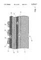
- FIG. 1is a representative elevational section of a ferroelectric heterostructure of the present invention
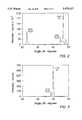
- FIG. 2is a representative X-ray diffraction pattern of a highly-oriented platinum layer obtained from template growth according to the present invention
- FIG. 3is a representative x-ray diffraction pattern of a weakly-oriented platinum layer resulting from non-template growth
- FIG. 4is a graph of comparative conductivities of ferroelectric heterostructures with and without a platinum ground layer according to the present invention.
- FIG. 5is a graph of comparative hysteresis loops obtained from testing ferroelectric heterostructures processed in different levels of atmospheric oxygen.
- FIG. 1A typical ferroelectric heterostructure memory element 10 prepared according to the present invention is shown in FIG. 1 comprising as a substrate a single crystal oriented [100] silicon wafer 11 the surface of which has been thermally wet oxidized to form an electronic grade amorphous SiO 2 layer 12 of about 100 nm thickness.
- a layer 13 of about 50 nm of bismuth titanate (BTO), typically Bi 4 Ti 3 O 12was grown a layer 13 of about 50 nm of bismuth titanate (BTO), typically Bi 4 Ti 3 O 12 , using pulsed laser deposition (PLD), although other common techniques, such as sputtering, chemical vapor deposition (CVD), and electron-beam deposition, could similarly be employed.
- BTObismuth titanate
- PLDpulsed laser deposition
- the c-axis orientation of the BTO layerwas confirmed by x-ray diffraction testing and the sample was mounted in an ion-beam deposition chamber where, at a temperature of about 450°-600° C., a 50-150 nm layer 14 of platinum metal was grown on the BTO template layer 13. X-ray diffraction examination confirmed that the platinum was very strongly (002) oriented.
- a first electrode layer 15 of LSCOtypically La 0 .5 Sr 0 .5 CoO 3
- a first electrode layer 15 of LSCOtypically La 0 .5 Sr 0 .5 CoO 3
- a ferroelectric layer 16 of PLZTfollowed at about 100-500 nm, typically 300 nm.
- the composition of the PLZT materialwas Pb 0 .9 La 0 .1 Zr 0 .2 Ti 0 .8 O 3 in this example, but could be varied over a wide range depending on the intended application.
- Other ferroelectric materialssuch as barium titanate, barium strontium titanate, and bismuth titanate, could similarly be employed for layer 16 in high dielectric constant capacitor applications and in pyroelectric detectors.
- a top electrode layer 17 of about 100 nm LSCOwas then grown and the completed heterostructure was cooled to ambient temperature at an optimum rate of about 10°-20° C./min in an atmosphere of about 1 ⁇ 10 5 Pa O 2 .
- X-ray diffraction examination of the completed heterostructureconfirmed that the ferroelectric stack was fully c-axis oriented.
- test capacitor electrodes 18were fashioned of the upper LSCO layer 17 upon which Pt/Au electrical contacts 19 were deposited. Complementary contact with bottom electrode layer 15 was established by capacitive coupling through a large conductive pad, not shown, elsewhere on the surface of the structure.
- Typical ferroelectric testing of the capacitor heterostructureshowed very desirable fatigue, aging, and retention properties which were eminently suitable for long term, non-volatile memory application. Remnant polarization values of about 15°-20° C./cm 2 at 5 V exhibited by the device are quite sufficient for this purpose. Additional testing at more extreme conditions of elevated temperature and the presence of dc bias showed equally satisfactory results. At about 100° C., for example, the device showed good read-write endurance over at least 10 11 cycles.
- Additional heterostructureswere grown to provide samples for testing the efficacy of the processing of the present invention.
- a first heterostructurewas prepared as described above to include template BTO layer 13 while in a second sample the Pt layer 14 was grown directly on SiO 2 layer 12.
- Respective x-ray diffraction patterns of the samples depicted in FIGS. 2 and 3show the strong orientation, particularly in the Pt and PLZT layers (FIG. 2), achieved from the use of the template layer, and the weak orientation (FIG. 3) resulting from the growth of Pt on the SiO 2 .
- the respective intensities of the patternsare particularly remarkable.
- a second set of samplesdiffered in the inclusion of Pt layer 14 beneath LSCO electrode 15 of the ferroelectric heterostructure stack. The difference in conductivity (resistance) between these samples is depicted in the traces of FIG. 4.
- ferroelectric heterostructure capacitor materials of the present inventionhave application for a wide range of devices, such as dielectrics for DRAM capacitors, ferroelectric FET elements for non-destructive readout memories, and electro-optic perovskites grown on SiO 2 /Si substrates for integrated optics, pyroelectric detectors, and the like.
- Another important aspect of the template growth techniqueis that the highly-oriented Pt layer will provide the basis for other oriented, and even epitaxial, metallic heterostructures, such as [001] oriented Fe/Pt superlattices for magneto-optic recording in information storage.
- MRAMmagnetoresistive random access memories
- magnetic recording and sensing elementsmay be realized through the integration of ferroelectrics and transistor circuitry enabled by the present invention.
Landscapes
- Semiconductor Memories (AREA)
Abstract
Description
Claims (10)
Priority Applications (1)
| Application Number | Priority Date | Filing Date | Title |
|---|---|---|---|
| US08/318,587US5479317A (en) | 1994-10-05 | 1994-10-05 | Ferroelectric capacitor heterostructure and method of making same |
Applications Claiming Priority (1)
| Application Number | Priority Date | Filing Date | Title |
|---|---|---|---|
| US08/318,587US5479317A (en) | 1994-10-05 | 1994-10-05 | Ferroelectric capacitor heterostructure and method of making same |
Publications (1)
| Publication Number | Publication Date |
|---|---|
| US5479317Atrue US5479317A (en) | 1995-12-26 |
Family
ID=23238799
Family Applications (1)
| Application Number | Title | Priority Date | Filing Date |
|---|---|---|---|
| US08/318,587Expired - Fee RelatedUS5479317A (en) | 1994-10-05 | 1994-10-05 | Ferroelectric capacitor heterostructure and method of making same |
Country Status (1)
| Country | Link |
|---|---|
| US (1) | US5479317A (en) |
Cited By (64)
| Publication number | Priority date | Publication date | Assignee | Title |
|---|---|---|---|---|
| WO1996028844A1 (en)* | 1995-03-15 | 1996-09-19 | Radiant Technologies, Inc. | Method for making improved lsco stack electrode |
| WO1997023886A1 (en)* | 1995-12-26 | 1997-07-03 | Bell Communications Research, Inc. | Electrode structure and method of making for ferroelectric capacitor integrated on silicon |
| WO1997025745A1 (en)* | 1996-01-03 | 1997-07-17 | Bell Communications Research, Inc. | Platinum-free ferroelectric memory cell with intermetallic barrier layer and method of making same |
| GB2310318A (en)* | 1996-02-15 | 1997-08-20 | Siemens Ag | Ferroelectric device |
| US5838035A (en)* | 1995-06-28 | 1998-11-17 | Bell Communications Research, Inc. | Barrier layer for ferroelectric capacitor integrated on silicon |
| EP0883167A3 (en)* | 1997-05-06 | 1999-07-21 | Tong Yang Cement Corporation | Forming preferred orientation-controlled platinum film using oxygen |
| US5972108A (en)* | 1997-08-13 | 1999-10-26 | Texas Instruments Incorporated | Method of preferentially-ordering a thermally sensitive element |
| US6034392A (en)* | 1998-06-03 | 2000-03-07 | Lg Semicon Co., Ltd. | Semiconductor device having capacitor |
| US6071787A (en)* | 1998-03-05 | 2000-06-06 | Lg Semicon Co., Ltd. | Method of forming a capacitor including forming a first and second conductive layers and etching layers to form alloyed conductive sidewall spacers |
| US6128178A (en)* | 1998-07-20 | 2000-10-03 | International Business Machines Corporation | Very thin film capacitor for dynamic random access memory (DRAM) |
| US6194754B1 (en)* | 1999-03-05 | 2001-02-27 | Telcordia Technologies, Inc. | Amorphous barrier layer in a ferroelectric memory cell |
| US6323512B1 (en)* | 1999-03-10 | 2001-11-27 | Tae-Won Noh | Nonvolatile ferroelectric capacitor and nonvolatile ferroelectric memory |
| US6351006B1 (en)* | 1998-11-10 | 2002-02-26 | Kabushiki Kaisha Toshiba | Ferroelectric capacitor with means to prevent deterioration |
| US6440591B1 (en)* | 1995-06-09 | 2002-08-27 | Sharp Kabushiki Kaisha | Ferroelectric thin film coated substrate, producing method thereof and capacitor structure element using thereof |
| US6500568B1 (en)* | 2001-06-06 | 2002-12-31 | 3M Innovative Properties Company | Biaxially textured metal substrate with palladium layer |
| WO2002009151A3 (en)* | 2000-07-24 | 2003-01-16 | Motorola Inc | Magnetoresistive structure |
| US6509070B1 (en)* | 2000-09-22 | 2003-01-21 | The United States Of America As Represented By The Secretary Of The Air Force | Laser ablation, low temperature-fabricated yttria-stabilized zirconia oriented films |
| US6531740B2 (en)* | 2001-07-17 | 2003-03-11 | Motorola, Inc. | Integrated impedance matching and stability network |
| US6555946B1 (en) | 2000-07-24 | 2003-04-29 | Motorola, Inc. | Acoustic wave device and process for forming the same |
| WO2002047127A3 (en)* | 2000-12-08 | 2003-06-19 | Motorola Inc | Pyroelectric device on a monocrystalline semiconductor substrate |
| US6589856B2 (en) | 2001-08-06 | 2003-07-08 | Motorola, Inc. | Method and apparatus for controlling anti-phase domains in semiconductor structures and devices |
| WO2003010834A3 (en)* | 2001-07-25 | 2003-07-24 | Motorola Inc | Microelectronic piezoelectric structure |
| US20030183859A1 (en)* | 2000-08-24 | 2003-10-02 | Gnadinger Fred P. | Single transistor rare earth manganite ferroelectric nonvolatile memory cell |
| US6639249B2 (en) | 2001-08-06 | 2003-10-28 | Motorola, Inc. | Structure and method for fabrication for a solid-state lighting device |
| US6638838B1 (en) | 2000-10-02 | 2003-10-28 | Motorola, Inc. | Semiconductor structure including a partially annealed layer and method of forming the same |
| US6646293B2 (en) | 2001-07-18 | 2003-11-11 | Motorola, Inc. | Structure for fabricating high electron mobility transistors utilizing the formation of complaint substrates |
| US6667196B2 (en) | 2001-07-25 | 2003-12-23 | Motorola, Inc. | Method for real-time monitoring and controlling perovskite oxide film growth and semiconductor structure formed using the method |
| US6674110B2 (en) | 2001-03-02 | 2004-01-06 | Cova Technologies, Inc. | Single transistor ferroelectric memory cell, device and method for the formation of the same incorporating a high temperature ferroelectric gate dielectric |
| US6673667B2 (en) | 2001-08-15 | 2004-01-06 | Motorola, Inc. | Method for manufacturing a substantially integral monolithic apparatus including a plurality of semiconductor materials |
| US6673646B2 (en) | 2001-02-28 | 2004-01-06 | Motorola, Inc. | Growth of compound semiconductor structures on patterned oxide films and process for fabricating same |
| US6693298B2 (en) | 2001-07-20 | 2004-02-17 | Motorola, Inc. | Structure and method for fabricating epitaxial semiconductor on insulator (SOI) structures and devices utilizing the formation of a compliant substrate for materials used to form same |
| US6693033B2 (en) | 2000-02-10 | 2004-02-17 | Motorola, Inc. | Method of removing an amorphous oxide from a monocrystalline surface |
| US20040041186A1 (en)* | 2002-08-28 | 2004-03-04 | Klaus Dimmler | Ferroelectric transistor with enhanced data retention |
| US6709989B2 (en) | 2001-06-21 | 2004-03-23 | Motorola, Inc. | Method for fabricating a semiconductor structure including a metal oxide interface with silicon |
| US6714435B1 (en) | 2002-09-19 | 2004-03-30 | Cova Technologies, Inc. | Ferroelectric transistor for storing two data bits |
| US20040217444A1 (en)* | 2001-10-17 | 2004-11-04 | Motorola, Inc. | Method and apparatus utilizing monocrystalline insulator |
| US6855992B2 (en) | 2001-07-24 | 2005-02-15 | Motorola Inc. | Structure and method for fabricating configurable transistor devices utilizing the formation of a compliant substrate for materials used to form the same |
| US6885065B2 (en) | 2002-11-20 | 2005-04-26 | Freescale Semiconductor, Inc. | Ferromagnetic semiconductor structure and method for forming the same |
| US6888736B2 (en) | 2002-09-19 | 2005-05-03 | Cova Technologies, Inc. | Ferroelectric transistor for storing two data bits |
| US6916717B2 (en) | 2002-05-03 | 2005-07-12 | Motorola, Inc. | Method for growing a monocrystalline oxide layer and for fabricating a semiconductor device on a monocrystalline substrate |
| US6965128B2 (en) | 2003-02-03 | 2005-11-15 | Freescale Semiconductor, Inc. | Structure and method for fabricating semiconductor microresonator devices |
| US6992321B2 (en) | 2001-07-13 | 2006-01-31 | Motorola, Inc. | Structure and method for fabricating semiconductor structures and devices utilizing piezoelectric materials |
| US7005717B2 (en) | 2000-05-31 | 2006-02-28 | Freescale Semiconductor, Inc. | Semiconductor device and method |
| US7020374B2 (en) | 2003-02-03 | 2006-03-28 | Freescale Semiconductor, Inc. | Optical waveguide structure and method for fabricating the same |
| US7019332B2 (en) | 2001-07-20 | 2006-03-28 | Freescale Semiconductor, Inc. | Fabrication of a wavelength locker within a semiconductor structure |
| US7045815B2 (en) | 2001-04-02 | 2006-05-16 | Freescale Semiconductor, Inc. | Semiconductor structure exhibiting reduced leakage current and method of fabricating same |
| US7067856B2 (en) | 2000-02-10 | 2006-06-27 | Freescale Semiconductor, Inc. | Semiconductor structure, semiconductor device, communicating device, integrated circuit, and process for fabricating the same |
| US7105866B2 (en) | 2000-07-24 | 2006-09-12 | Freescale Semiconductor, Inc. | Heterojunction tunneling diodes and process for fabricating same |
| US7161227B2 (en) | 2001-08-14 | 2007-01-09 | Motorola, Inc. | Structure and method for fabricating semiconductor structures and devices for detecting an object |
| US7169619B2 (en) | 2002-11-19 | 2007-01-30 | Freescale Semiconductor, Inc. | Method for fabricating semiconductor structures on vicinal substrates using a low temperature, low pressure, alkaline earth metal-rich process |
| US7211852B2 (en) | 2001-01-19 | 2007-05-01 | Freescale Semiconductor, Inc. | Structure and method for fabricating GaN devices utilizing the formation of a compliant substrate |
| US20080062615A1 (en)* | 2006-07-07 | 2008-03-13 | The Trustees Of The University Of Pennsylvania | Ferroelectric thin films |
| US20080106846A1 (en)* | 2002-05-15 | 2008-05-08 | Raytheon Company | Electrode for thin film capacitor devices |
| US20100157657A1 (en)* | 2004-02-06 | 2010-06-24 | Unity Semiconductor Corporation | Multi-resistive state memory device with conductive oxide electrodes |
| US20100291378A1 (en)* | 2006-12-01 | 2010-11-18 | The Trustees Of The University Of Pennsylvania | Ferroelectric ultrathin perovskite films |
| US10186595B2 (en) | 2016-08-05 | 2019-01-22 | Northwestern University | Noncentrosymmetric metal electrodes for ferroic devices |
| US10680171B2 (en) | 2004-02-06 | 2020-06-09 | Hefei Reliance Memory Limited | Two-terminal reversibly switchable memory device |
| CN111276602A (en)* | 2020-02-14 | 2020-06-12 | 北京工业大学 | A kind of non-volatile resistive memory based on bismuth tungstate material |
| US11164976B2 (en) | 2019-04-08 | 2021-11-02 | Kepler Computing Inc. | Doped polar layers and semiconductor device incorporating same |
| US11289542B2 (en) | 2011-09-30 | 2022-03-29 | Hefei Reliance Memory Limited | Multi-layered conductive metal oxide structures and methods for facilitating enhanced performance characteristics of two-terminal memory cells |
| US11289497B2 (en) | 2019-12-27 | 2022-03-29 | Kepler Computing Inc. | Integration method of ferroelectric memory array |
| US11430861B2 (en) | 2019-12-27 | 2022-08-30 | Kepler Computing Inc. | Ferroelectric capacitor and method of patterning such |
| US11482528B2 (en) | 2019-12-27 | 2022-10-25 | Kepler Computing Inc. | Pillar capacitor and method of fabricating such |
| US11765909B1 (en) | 2021-06-11 | 2023-09-19 | Kepler Computing Inc. | Process integration flow for embedded memory enabled by decoupling processing of a memory area from a non-memory area |
Citations (5)
| Publication number | Priority date | Publication date | Assignee | Title |
|---|---|---|---|---|
| US5005102A (en)* | 1989-06-20 | 1991-04-02 | Ramtron Corporation | Multilayer electrodes for integrated circuit capacitors |
| US5155658A (en)* | 1992-03-05 | 1992-10-13 | Bell Communications Research, Inc. | Crystallographically aligned ferroelectric films usable in memories and method of crystallographically aligning perovskite films |
| US5169485A (en)* | 1991-03-07 | 1992-12-08 | Bell Communications Research, Inc. | Method for the preparation of epitaxial ferromagnetic manganese aluminum magnetic memory element |
| US5248564A (en)* | 1992-12-09 | 1993-09-28 | Bell Communications Research, Inc. | C-axis perovskite thin films grown on silicon dioxide |
| US5270298A (en)* | 1992-03-05 | 1993-12-14 | Bell Communications Research, Inc. | Cubic metal oxide thin film epitaxially grown on silicon |
- 1994
- 1994-10-05USUS08/318,587patent/US5479317A/ennot_activeExpired - Fee Related
Patent Citations (5)
| Publication number | Priority date | Publication date | Assignee | Title |
|---|---|---|---|---|
| US5005102A (en)* | 1989-06-20 | 1991-04-02 | Ramtron Corporation | Multilayer electrodes for integrated circuit capacitors |
| US5169485A (en)* | 1991-03-07 | 1992-12-08 | Bell Communications Research, Inc. | Method for the preparation of epitaxial ferromagnetic manganese aluminum magnetic memory element |
| US5155658A (en)* | 1992-03-05 | 1992-10-13 | Bell Communications Research, Inc. | Crystallographically aligned ferroelectric films usable in memories and method of crystallographically aligning perovskite films |
| US5270298A (en)* | 1992-03-05 | 1993-12-14 | Bell Communications Research, Inc. | Cubic metal oxide thin film epitaxially grown on silicon |
| US5248564A (en)* | 1992-12-09 | 1993-09-28 | Bell Communications Research, Inc. | C-axis perovskite thin films grown on silicon dioxide |
Cited By (121)
| Publication number | Priority date | Publication date | Assignee | Title |
|---|---|---|---|---|
| US5614438A (en)* | 1995-03-15 | 1997-03-25 | Radiant Technologies, Inc. | Method for making LSCO stack electrode |
| WO1996028844A1 (en)* | 1995-03-15 | 1996-09-19 | Radiant Technologies, Inc. | Method for making improved lsco stack electrode |
| US6440591B1 (en)* | 1995-06-09 | 2002-08-27 | Sharp Kabushiki Kaisha | Ferroelectric thin film coated substrate, producing method thereof and capacitor structure element using thereof |
| US5838035A (en)* | 1995-06-28 | 1998-11-17 | Bell Communications Research, Inc. | Barrier layer for ferroelectric capacitor integrated on silicon |
| WO1997023886A1 (en)* | 1995-12-26 | 1997-07-03 | Bell Communications Research, Inc. | Electrode structure and method of making for ferroelectric capacitor integrated on silicon |
| US5798903A (en)* | 1995-12-26 | 1998-08-25 | Bell Communications Research, Inc. | Electrode structure for ferroelectric capacitor integrated on silicon |
| WO1997025745A1 (en)* | 1996-01-03 | 1997-07-17 | Bell Communications Research, Inc. | Platinum-free ferroelectric memory cell with intermetallic barrier layer and method of making same |
| GB2310318A (en)* | 1996-02-15 | 1997-08-20 | Siemens Ag | Ferroelectric device |
| GB2310318B (en)* | 1996-02-15 | 2000-12-13 | Siemens Ag | Ferroelectric component and method of manufacture |
| EP0883167A3 (en)* | 1997-05-06 | 1999-07-21 | Tong Yang Cement Corporation | Forming preferred orientation-controlled platinum film using oxygen |
| US5972108A (en)* | 1997-08-13 | 1999-10-26 | Texas Instruments Incorporated | Method of preferentially-ordering a thermally sensitive element |
| US6071787A (en)* | 1998-03-05 | 2000-06-06 | Lg Semicon Co., Ltd. | Method of forming a capacitor including forming a first and second conductive layers and etching layers to form alloyed conductive sidewall spacers |
| US6034392A (en)* | 1998-06-03 | 2000-03-07 | Lg Semicon Co., Ltd. | Semiconductor device having capacitor |
| US6242316B1 (en) | 1998-06-03 | 2001-06-05 | Hyundai Electronics Industries Co., Ltd. | Semiconductor device having capacitor and method of fabricating the same |
| US6128178A (en)* | 1998-07-20 | 2000-10-03 | International Business Machines Corporation | Very thin film capacitor for dynamic random access memory (DRAM) |
| US6351006B1 (en)* | 1998-11-10 | 2002-02-26 | Kabushiki Kaisha Toshiba | Ferroelectric capacitor with means to prevent deterioration |
| US6194754B1 (en)* | 1999-03-05 | 2001-02-27 | Telcordia Technologies, Inc. | Amorphous barrier layer in a ferroelectric memory cell |
| US6610549B1 (en)* | 1999-03-05 | 2003-08-26 | University Of Maryland, College Park | Amorphous barrier layer in a ferroelectric memory cell |
| US6323512B1 (en)* | 1999-03-10 | 2001-11-27 | Tae-Won Noh | Nonvolatile ferroelectric capacitor and nonvolatile ferroelectric memory |
| US6693033B2 (en) | 2000-02-10 | 2004-02-17 | Motorola, Inc. | Method of removing an amorphous oxide from a monocrystalline surface |
| US7067856B2 (en) | 2000-02-10 | 2006-06-27 | Freescale Semiconductor, Inc. | Semiconductor structure, semiconductor device, communicating device, integrated circuit, and process for fabricating the same |
| US7005717B2 (en) | 2000-05-31 | 2006-02-28 | Freescale Semiconductor, Inc. | Semiconductor device and method |
| WO2002009151A3 (en)* | 2000-07-24 | 2003-01-16 | Motorola Inc | Magnetoresistive structure |
| US6555946B1 (en) | 2000-07-24 | 2003-04-29 | Motorola, Inc. | Acoustic wave device and process for forming the same |
| US7105866B2 (en) | 2000-07-24 | 2006-09-12 | Freescale Semiconductor, Inc. | Heterojunction tunneling diodes and process for fabricating same |
| US20030183859A1 (en)* | 2000-08-24 | 2003-10-02 | Gnadinger Fred P. | Single transistor rare earth manganite ferroelectric nonvolatile memory cell |
| US7030435B2 (en) | 2000-08-24 | 2006-04-18 | Cova Technologies, Inc. | Single transistor rare earth manganite ferroelectric nonvolatile memory cell |
| US6509070B1 (en)* | 2000-09-22 | 2003-01-21 | The United States Of America As Represented By The Secretary Of The Air Force | Laser ablation, low temperature-fabricated yttria-stabilized zirconia oriented films |
| US6638838B1 (en) | 2000-10-02 | 2003-10-28 | Motorola, Inc. | Semiconductor structure including a partially annealed layer and method of forming the same |
| WO2002047127A3 (en)* | 2000-12-08 | 2003-06-19 | Motorola Inc | Pyroelectric device on a monocrystalline semiconductor substrate |
| US7211852B2 (en) | 2001-01-19 | 2007-05-01 | Freescale Semiconductor, Inc. | Structure and method for fabricating GaN devices utilizing the formation of a compliant substrate |
| US6673646B2 (en) | 2001-02-28 | 2004-01-06 | Motorola, Inc. | Growth of compound semiconductor structures on patterned oxide films and process for fabricating same |
| US6674110B2 (en) | 2001-03-02 | 2004-01-06 | Cova Technologies, Inc. | Single transistor ferroelectric memory cell, device and method for the formation of the same incorporating a high temperature ferroelectric gate dielectric |
| US7045815B2 (en) | 2001-04-02 | 2006-05-16 | Freescale Semiconductor, Inc. | Semiconductor structure exhibiting reduced leakage current and method of fabricating same |
| US6500568B1 (en)* | 2001-06-06 | 2002-12-31 | 3M Innovative Properties Company | Biaxially textured metal substrate with palladium layer |
| US6709989B2 (en) | 2001-06-21 | 2004-03-23 | Motorola, Inc. | Method for fabricating a semiconductor structure including a metal oxide interface with silicon |
| US6992321B2 (en) | 2001-07-13 | 2006-01-31 | Motorola, Inc. | Structure and method for fabricating semiconductor structures and devices utilizing piezoelectric materials |
| US6531740B2 (en)* | 2001-07-17 | 2003-03-11 | Motorola, Inc. | Integrated impedance matching and stability network |
| US6646293B2 (en) | 2001-07-18 | 2003-11-11 | Motorola, Inc. | Structure for fabricating high electron mobility transistors utilizing the formation of complaint substrates |
| US6693298B2 (en) | 2001-07-20 | 2004-02-17 | Motorola, Inc. | Structure and method for fabricating epitaxial semiconductor on insulator (SOI) structures and devices utilizing the formation of a compliant substrate for materials used to form same |
| US7019332B2 (en) | 2001-07-20 | 2006-03-28 | Freescale Semiconductor, Inc. | Fabrication of a wavelength locker within a semiconductor structure |
| US6855992B2 (en) | 2001-07-24 | 2005-02-15 | Motorola Inc. | Structure and method for fabricating configurable transistor devices utilizing the formation of a compliant substrate for materials used to form the same |
| US6667196B2 (en) | 2001-07-25 | 2003-12-23 | Motorola, Inc. | Method for real-time monitoring and controlling perovskite oxide film growth and semiconductor structure formed using the method |
| WO2003010834A3 (en)* | 2001-07-25 | 2003-07-24 | Motorola Inc | Microelectronic piezoelectric structure |
| US6589856B2 (en) | 2001-08-06 | 2003-07-08 | Motorola, Inc. | Method and apparatus for controlling anti-phase domains in semiconductor structures and devices |
| US6639249B2 (en) | 2001-08-06 | 2003-10-28 | Motorola, Inc. | Structure and method for fabrication for a solid-state lighting device |
| US7161227B2 (en) | 2001-08-14 | 2007-01-09 | Motorola, Inc. | Structure and method for fabricating semiconductor structures and devices for detecting an object |
| US6673667B2 (en) | 2001-08-15 | 2004-01-06 | Motorola, Inc. | Method for manufacturing a substantially integral monolithic apparatus including a plurality of semiconductor materials |
| US7342276B2 (en) | 2001-10-17 | 2008-03-11 | Freescale Semiconductor, Inc. | Method and apparatus utilizing monocrystalline insulator |
| US20040217444A1 (en)* | 2001-10-17 | 2004-11-04 | Motorola, Inc. | Method and apparatus utilizing monocrystalline insulator |
| US6916717B2 (en) | 2002-05-03 | 2005-07-12 | Motorola, Inc. | Method for growing a monocrystalline oxide layer and for fabricating a semiconductor device on a monocrystalline substrate |
| US20080106846A1 (en)* | 2002-05-15 | 2008-05-08 | Raytheon Company | Electrode for thin film capacitor devices |
| US7545625B2 (en)* | 2002-05-15 | 2009-06-09 | Raytheon Company | Electrode for thin film capacitor devices |
| US20040041186A1 (en)* | 2002-08-28 | 2004-03-04 | Klaus Dimmler | Ferroelectric transistor with enhanced data retention |
| US6790679B2 (en) | 2002-08-28 | 2004-09-14 | Cova Technologies, Inc. | Ferroelectric transistor with enhanced data retention |
| US6825517B2 (en) | 2002-08-28 | 2004-11-30 | Cova Technologies, Inc. | Ferroelectric transistor with enhanced data retention |
| US6888736B2 (en) | 2002-09-19 | 2005-05-03 | Cova Technologies, Inc. | Ferroelectric transistor for storing two data bits |
| US6714435B1 (en) | 2002-09-19 | 2004-03-30 | Cova Technologies, Inc. | Ferroelectric transistor for storing two data bits |
| US7034349B2 (en) | 2002-09-19 | 2006-04-25 | Cova Technologies, Inc. | Ferroelectric transistor for storing two data bits |
| US7169619B2 (en) | 2002-11-19 | 2007-01-30 | Freescale Semiconductor, Inc. | Method for fabricating semiconductor structures on vicinal substrates using a low temperature, low pressure, alkaline earth metal-rich process |
| US6885065B2 (en) | 2002-11-20 | 2005-04-26 | Freescale Semiconductor, Inc. | Ferromagnetic semiconductor structure and method for forming the same |
| US6965128B2 (en) | 2003-02-03 | 2005-11-15 | Freescale Semiconductor, Inc. | Structure and method for fabricating semiconductor microresonator devices |
| US7020374B2 (en) | 2003-02-03 | 2006-03-28 | Freescale Semiconductor, Inc. | Optical waveguide structure and method for fabricating the same |
| US9570515B2 (en) | 2004-02-06 | 2017-02-14 | Unity Semiconductor Corporation | Memory element with a reactive metal layer |
| US9806130B2 (en) | 2004-02-06 | 2017-10-31 | Unity Semiconductor Corporation | Memory element with a reactive metal layer |
| US11502249B2 (en) | 2004-02-06 | 2022-11-15 | Hefei Reliance Memory Limited | Memory element with a reactive metal layer |
| US11672189B2 (en) | 2004-02-06 | 2023-06-06 | Hefei Reliance Memory Limited | Two-terminal reversibly switchable memory device |
| US11063214B2 (en) | 2004-02-06 | 2021-07-13 | Hefei Reliance Memory Limited | Two-terminal reversibly switchable memory device |
| US7889539B2 (en)* | 2004-02-06 | 2011-02-15 | Unity Semiconductor Corporation | Multi-resistive state memory device with conductive oxide electrodes |
| US20110186803A1 (en)* | 2004-02-06 | 2011-08-04 | Unity Semiconductor Corporation | Multi-resistive state memory device with conductive oxide electrodes |
| US10833125B2 (en) | 2004-02-06 | 2020-11-10 | Hefei Reliance Memory Limited | Memory element with a reactive metal layer |
| US10680171B2 (en) | 2004-02-06 | 2020-06-09 | Hefei Reliance Memory Limited | Two-terminal reversibly switchable memory device |
| US9159408B2 (en) | 2004-02-06 | 2015-10-13 | Unity Semiconductor Corporation | Memory element with a reactive metal layer |
| US10340312B2 (en) | 2004-02-06 | 2019-07-02 | Hefei Reliance Memory Limited | Memory element with a reactive metal layer |
| US20100157657A1 (en)* | 2004-02-06 | 2010-06-24 | Unity Semiconductor Corporation | Multi-resistive state memory device with conductive oxide electrodes |
| US20080062615A1 (en)* | 2006-07-07 | 2008-03-13 | The Trustees Of The University Of Pennsylvania | Ferroelectric thin films |
| US8022454B2 (en) | 2006-07-07 | 2011-09-20 | The Trustees Of The University Of Pennsylvania | Ferroelectric thin films |
| US20100252901A1 (en)* | 2006-07-07 | 2010-10-07 | The Trustees Of The University Of Pennsylvania | Ferroelectric thin films |
| US7768050B2 (en) | 2006-07-07 | 2010-08-03 | The Trustees Of The University Of Pennsylvania | Ferroelectric thin films |
| US8603573B2 (en)* | 2006-12-01 | 2013-12-10 | The Trustees Of The University Of Pennsylvania | Ferroelectric ultrathin perovskite films |
| US20100291378A1 (en)* | 2006-12-01 | 2010-11-18 | The Trustees Of The University Of Pennsylvania | Ferroelectric ultrathin perovskite films |
| US11765914B2 (en) | 2011-09-30 | 2023-09-19 | Hefei Reliance Memory Limited | Multi-layered conductive metal oxide structures and methods for facilitating enhanced performance characteristics of two-terminal memory cells |
| US11289542B2 (en) | 2011-09-30 | 2022-03-29 | Hefei Reliance Memory Limited | Multi-layered conductive metal oxide structures and methods for facilitating enhanced performance characteristics of two-terminal memory cells |
| US10186595B2 (en) | 2016-08-05 | 2019-01-22 | Northwestern University | Noncentrosymmetric metal electrodes for ferroic devices |
| US11296228B2 (en) | 2019-04-08 | 2022-04-05 | Kepler Computing Inc. | Doped polar layers and semiconductor device incorporating same |
| US11916149B2 (en) | 2019-04-08 | 2024-02-27 | Kepler Computing Inc. | Doped polar layers and semiconductor device incorporating same |
| US11289608B2 (en) | 2019-04-08 | 2022-03-29 | Kepler Computing Inc. | Doped polar layers and semiconductor device incorporating same |
| US11349031B2 (en) | 2019-04-08 | 2022-05-31 | Kepler Computing Inc. | Doped polar layers and semiconductor device incorporating same |
| US11355643B2 (en) | 2019-04-08 | 2022-06-07 | Kepler Computing Inc. | Doped polar layers and semiconductor device incorporating same |
| US11398570B2 (en) | 2019-04-08 | 2022-07-26 | Kepler Computing Inc. | Doped polar layers and semiconductor device incorporating same |
| US11411116B2 (en) | 2019-04-08 | 2022-08-09 | Kepler Computing Inc. | Doped polar layers and semiconductor device incorporating same |
| US11417768B2 (en) | 2019-04-08 | 2022-08-16 | Kepler Computing Inc. | Doped polar layers and semiconductor device incorporating same |
| US12369351B2 (en) | 2019-04-08 | 2025-07-22 | Kepler Computing Inc. | Doped polar layers and semiconductor device incorporating same |
| US11444203B2 (en) | 2019-04-08 | 2022-09-13 | Kepler Computing Inc. | Doped polar layers and semiconductor device incorporating same |
| US11469327B2 (en) | 2019-04-08 | 2022-10-11 | Kepler Computing Inc. | Doped polar layers and semiconductor device incorporating same |
| US12294029B2 (en) | 2019-04-08 | 2025-05-06 | Kepler Computing Inc. | Doped polar layers and semiconductor device incorporating same |
| US11289607B2 (en) | 2019-04-08 | 2022-03-29 | Kepler Computing Inc. | Doped polar layers and semiconductor device incorporating same |
| US11949018B2 (en) | 2019-04-08 | 2024-04-02 | Kepler Computing Inc. | Doped polar layers and semiconductor device incorporating same |
| US11949017B2 (en) | 2019-04-08 | 2024-04-02 | Kepler Computing Inc. | Doped polar layers and semiconductor device incorporating same |
| US11164976B2 (en) | 2019-04-08 | 2021-11-02 | Kepler Computing Inc. | Doped polar layers and semiconductor device incorporating same |
| US11757043B2 (en) | 2019-04-08 | 2023-09-12 | Kepler Computing Inc. | Doped polar layers and semiconductor device incorporating same |
| US11908943B2 (en) | 2019-04-08 | 2024-02-20 | Kepler Computing Inc. | Manganese-doped perovskite layers and semiconductor device incorporating same |
| US11888066B2 (en) | 2019-04-08 | 2024-01-30 | Kepler Computing Inc. | Doped polar layers and semiconductor device incorporating same |
| US11888067B2 (en) | 2019-04-08 | 2024-01-30 | Kepler Computing Inc. | B-site doped perovskite layers and semiconductor device incorporating same |
| US11848386B2 (en) | 2019-04-08 | 2023-12-19 | Kepler Computing Inc. | B-site doped perovskite layers and semiconductor device incorporating same |
| US11837664B2 (en) | 2019-04-08 | 2023-12-05 | Kepler Computing Inc. | Doped polar layers and semiconductor device incorporating same |
| US12113097B2 (en) | 2019-12-27 | 2024-10-08 | Kepler Computing Inc. | Ferroelectric capacitor integrated with logic |
| US11641747B2 (en) | 2019-12-27 | 2023-05-02 | Kepler Computing Inc. | Integration of a ferroelectric memory device with a transistor |
| US11430861B2 (en) | 2019-12-27 | 2022-08-30 | Kepler Computing Inc. | Ferroelectric capacitor and method of patterning such |
| US11482528B2 (en) | 2019-12-27 | 2022-10-25 | Kepler Computing Inc. | Pillar capacitor and method of fabricating such |
| US12200941B2 (en) | 2019-12-27 | 2025-01-14 | Kepler Computing Inc. | Pillar capacitor and method of fabricating such |
| US11758738B2 (en) | 2019-12-27 | 2023-09-12 | Kepler Computing Inc. | Integration of ferroelectric memory devices with transistors |
| US11522044B2 (en) | 2019-12-27 | 2022-12-06 | Kepler Computing Inc. | Ferroelectric capacitor integrated with logic |
| US12137574B2 (en) | 2019-12-27 | 2024-11-05 | Kepler Computing Inc. | Integration of ferroelectric memory devices having stacked electrodes with transistors |
| US11289497B2 (en) | 2019-12-27 | 2022-03-29 | Kepler Computing Inc. | Integration method of ferroelectric memory array |
| CN111276602A (en)* | 2020-02-14 | 2020-06-12 | 北京工业大学 | A kind of non-volatile resistive memory based on bismuth tungstate material |
| CN111276602B (en)* | 2020-02-14 | 2023-09-26 | 北京工业大学 | Non-volatile resistive random access memory based on bismuth tungstate material |
| US11792998B1 (en) | 2021-06-11 | 2023-10-17 | Kepler Computing Inc. | Process integration flow for embedded memory with multi-pocket masks for decoupling processing of memory areas from non-memory areas |
| US11785782B1 (en) | 2021-06-11 | 2023-10-10 | Kepler Computing Inc. | Embedded memory with encapsulation layer adjacent to a memory stack |
| US11765909B1 (en) | 2021-06-11 | 2023-09-19 | Kepler Computing Inc. | Process integration flow for embedded memory enabled by decoupling processing of a memory area from a non-memory area |
| US12238935B1 (en) | 2021-06-11 | 2025-02-25 | Kepler Computing Inc. | Embedded memory adjacent to non-memory |
Similar Documents
| Publication | Publication Date | Title |
|---|---|---|
| US5479317A (en) | Ferroelectric capacitor heterostructure and method of making same | |
| EP0792524B1 (en) | Polycrystalline ferroelectric capacitor heterostructure employing hybrid electrodes | |
| MXPA97003547A (en) | Heteroestructura of polycrystalline ferroelectric capacitor that uses hybrid electrodes | |
| Lee et al. | Imprint of (Pb, La)(Zr, Ti) O3 thin films with various crystalline qualities | |
| Liu et al. | Epitaxial La-doped SrTiO 3 on silicon: A conductive template for epitaxial ferroelectrics on silicon | |
| EP0673311B1 (en) | C-axis perovskite thin films grown on silicon dioxide | |
| Ramesh et al. | Fatigue and retention in ferroelectric Y‐Ba‐Cu‐O/Pb‐Zr‐Ti‐O/Y‐Ba‐Cu‐O heterostructures | |
| EP0654169B1 (en) | Cubic metal oxide thin film epitaxially grown on silicon | |
| EP0747937B1 (en) | Method of forming a substrate coated with a ferroelectric thin film | |
| US5753934A (en) | Multilayer thin film, substrate for electronic device, electronic device, and preparation of multilayer oxide thin film | |
| Wang et al. | Epitaxial ferroelectric Pb (Zr, Ti) O 3 thin films on Si using SrTiO 3 template layers | |
| US7368172B2 (en) | Membrane multi-layer structure, and actuator element, capacitive element and filter element using the same | |
| KR100413618B1 (en) | Low imprint ferroelectric material for long retention memory and method of making the same | |
| US5889696A (en) | Thin-film capacitor device and RAM device using ferroelectric film | |
| EP0732422A2 (en) | Ferroelectric thin-film coated substrate, method for its manufacture and nonvolatile memory comprising such a substrate | |
| WO1993012542A1 (en) | Layered superlattice material applications | |
| JPH10269842A (en) | Conductive oxide thin film, thin film capacitor and magnetoresistive element | |
| US6307225B1 (en) | Insulating material, substrate covered with an insulating film, method of producing the same, and thin-film device | |
| Ramesh et al. | Template approaches to growth of oriented oxide heterostructures on SiO2/Si | |
| CA2203524C (en) | Polycrystalline ferroelectric capacitor heterostructure employing hybrid electrodes | |
| CN1164295A (en) | Polycrystalline Ferroelectric Capacitor Heterostructure Using Mixed Electrodes | |
| Ramesh et al. | Structure and properties of ferroelectric PbZr0. 2Ti0. 8O3/YBa2Cu3O7 heterostructures | |
| Lee et al. | Ferroelectric La-Sr-Co-O/Pb-La-Zr-Ti-O/La-Sr-Co-O heterostructures on silicon | |
| Chung et al. | Study on Multilayered Electrodes for Ferroelectric Thin Film Capacitors | |
| LEE et al. | HETEROSTRUCTURES ON SILICON |
Legal Events
| Date | Code | Title | Description |
|---|---|---|---|
| AS | Assignment | Owner name:BELL COMMUNICATIONS RESEARCH, INC., NEW JERSEY Free format text:ASSIGNMENT OF ASSIGNORS INTEREST;ASSIGNOR:RAMESH, RAMAMOORTHY;REEL/FRAME:007184/0806 Effective date:19941004 | |
| FEPP | Fee payment procedure | Free format text:PAYOR NUMBER ASSIGNED (ORIGINAL EVENT CODE: ASPN); ENTITY STATUS OF PATENT OWNER: SMALL ENTITY | |
| FPAY | Fee payment | Year of fee payment:4 | |
| AS | Assignment | Owner name:TELCORDIA TECHNOLOGIES, INC., NEW JERSEY Free format text:CHANGE OF NAME;ASSIGNOR:BELL COMMUNICATIONS RESEARCH, INC.;REEL/FRAME:010263/0311 Effective date:19990316 | |
| REMI | Maintenance fee reminder mailed | ||
| AS | Assignment | Owner name:UNIVERSITY OF MARYLAND, COLLEGE PARK, MARYLAND Free format text:ASSIGNMENT OF ASSIGNORS INTEREST;ASSIGNOR:TELCORDIA TECHNOLOGIES, INC.;REEL/FRAME:014074/0316 Effective date:20030228 | |
| FEPP | Fee payment procedure | Free format text:PAT HOLDER CLAIMS SMALL ENTITY STATUS, ENTITY STATUS SET TO SMALL (ORIGINAL EVENT CODE: LTOS); ENTITY STATUS OF PATENT OWNER: SMALL ENTITY | |
| FPAY | Fee payment | Year of fee payment:8 | |
| SULP | Surcharge for late payment | Year of fee payment:7 | |
| REMI | Maintenance fee reminder mailed | ||
| LAPS | Lapse for failure to pay maintenance fees | ||
| STCH | Information on status: patent discontinuation | Free format text:PATENT EXPIRED DUE TO NONPAYMENT OF MAINTENANCE FEES UNDER 37 CFR 1.362 | |
| FP | Lapsed due to failure to pay maintenance fee | Effective date:20071226 |