US5478773A - Method of making an electronic device having an integrated inductor - Google Patents
Method of making an electronic device having an integrated inductorDownload PDFInfo
- Publication number
- US5478773A US5478773AUS08/451,866US45186695AUS5478773AUS 5478773 AUS5478773 AUS 5478773AUS 45186695 AUS45186695 AUS 45186695AUS 5478773 AUS5478773 AUS 5478773A
- Authority
- US
- United States
- Prior art keywords
- layer
- copper
- copper layer
- etching
- sputtered
- Prior art date
- Legal status (The legal status is an assumption and is not a legal conclusion. Google has not performed a legal analysis and makes no representation as to the accuracy of the status listed.)
- Expired - Lifetime
Links
- 238000004519manufacturing processMethods0.000titleclaimsabstractdescription6
- 229910052802copperInorganic materials0.000claimsabstractdescription85
- 239000010949copperSubstances0.000claimsabstractdescription85
- RYGMFSIKBFXOCR-UHFFFAOYSA-NCopperChemical compound[Cu]RYGMFSIKBFXOCR-UHFFFAOYSA-N0.000claimsabstractdescription84
- 239000007787solidSubstances0.000claimsabstractdescription7
- 239000010410layerSubstances0.000claimsdescription126
- 238000000034methodMethods0.000claimsdescription28
- 238000005530etchingMethods0.000claimsdescription21
- 239000000758substrateSubstances0.000claimsdescription20
- 229910052751metalInorganic materials0.000claimsdescription12
- 239000002184metalSubstances0.000claimsdescription12
- 229920002120photoresistant polymerPolymers0.000claimsdescription11
- 239000004065semiconductorSubstances0.000claimsdescription11
- 229910052782aluminiumInorganic materials0.000claimsdescription10
- XAGFODPZIPBFFR-UHFFFAOYSA-NaluminiumChemical compound[Al]XAGFODPZIPBFFR-UHFFFAOYSA-N0.000claimsdescription10
- 230000008878couplingEffects0.000claimsdescription9
- 238000010168coupling processMethods0.000claimsdescription9
- 238000005859coupling reactionMethods0.000claimsdescription9
- MAKDTFFYCIMFQP-UHFFFAOYSA-Ntitanium tungstenChemical compound[Ti].[W]MAKDTFFYCIMFQP-UHFFFAOYSA-N0.000claimsdescription8
- 230000004888barrier functionEffects0.000claimsdescription7
- 238000009792diffusion processMethods0.000claimsdescription7
- 238000007747platingMethods0.000claimsdescription6
- 239000004642PolyimideSubstances0.000claimsdescription4
- 229920001721polyimidePolymers0.000claimsdescription4
- 238000000151depositionMethods0.000claimsdescription3
- 239000011241protective layerSubstances0.000claimsdescription3
- 238000004544sputter depositionMethods0.000claimsdescription3
- ROOXNKNUYICQNP-UHFFFAOYSA-Nammonium persulfateChemical compound[NH4+].[NH4+].[O-]S(=O)(=O)OOS([O-])(=O)=OROOXNKNUYICQNP-UHFFFAOYSA-N0.000claims6
- 229910001870ammonium persulfateInorganic materials0.000claims3
- 235000019395ammonium persulphateNutrition0.000claims3
- 238000000059patterningMethods0.000claims2
- 230000008901benefitEffects0.000abstractdescription3
- 239000000463materialSubstances0.000description6
- 230000003071parasitic effectEffects0.000description5
- PCHJSUWPFVWCPO-UHFFFAOYSA-NgoldChemical compound[Au]PCHJSUWPFVWCPO-UHFFFAOYSA-N0.000description4
- 229910052737goldInorganic materials0.000description4
- 239000010931goldSubstances0.000description4
- ATJFFYVFTNAWJD-UHFFFAOYSA-NTinChemical compound[Sn]ATJFFYVFTNAWJD-UHFFFAOYSA-N0.000description3
- 230000008569processEffects0.000description3
- VYPSYNLAJGMNEJ-UHFFFAOYSA-NSilicium dioxideChemical compoundO=[Si]=OVYPSYNLAJGMNEJ-UHFFFAOYSA-N0.000description2
- 238000010276constructionMethods0.000description2
- 230000008021depositionEffects0.000description2
- 238000005516engineering processMethods0.000description2
- 238000001465metallisationMethods0.000description2
- 238000012986modificationMethods0.000description2
- 230000004048modificationEffects0.000description2
- 238000003672processing methodMethods0.000description2
- 229910001218Gallium arsenideInorganic materials0.000description1
- 229910045601alloyInorganic materials0.000description1
- 239000000956alloySubstances0.000description1
- 238000013459approachMethods0.000description1
- 239000003990capacitorSubstances0.000description1
- 238000005229chemical vapour depositionMethods0.000description1
- 229910052681coesiteInorganic materials0.000description1
- 238000004891communicationMethods0.000description1
- 150000001875compoundsChemical class0.000description1
- 229910052906cristobaliteInorganic materials0.000description1
- 238000009713electroplatingMethods0.000description1
- 230000007613environmental effectEffects0.000description1
- 238000001914filtrationMethods0.000description1
- -1for exampleSubstances0.000description1
- 150000002739metalsChemical class0.000description1
- 238000000465mouldingMethods0.000description1
- 238000005457optimizationMethods0.000description1
- 244000045947parasiteSpecies0.000description1
- 230000000135prohibitive effectEffects0.000description1
- 239000000377silicon dioxideSubstances0.000description1
- 229910052682stishoviteInorganic materials0.000description1
- 229910052905tridymiteInorganic materials0.000description1
Images
Classifications
- H—ELECTRICITY
- H10—SEMICONDUCTOR DEVICES; ELECTRIC SOLID-STATE DEVICES NOT OTHERWISE PROVIDED FOR
- H10D—INORGANIC ELECTRIC SEMICONDUCTOR DEVICES
- H10D84/00—Integrated devices formed in or on semiconductor substrates that comprise only semiconducting layers, e.g. on Si wafers or on GaAs-on-Si wafers
- H—ELECTRICITY
- H01—ELECTRIC ELEMENTS
- H01L—SEMICONDUCTOR DEVICES NOT COVERED BY CLASS H10
- H01L23/00—Details of semiconductor or other solid state devices
- H01L23/52—Arrangements for conducting electric current within the device in operation from one component to another, i.e. interconnections, e.g. wires, lead frames
- H01L23/522—Arrangements for conducting electric current within the device in operation from one component to another, i.e. interconnections, e.g. wires, lead frames including external interconnections consisting of a multilayer structure of conductive and insulating layers inseparably formed on the semiconductor body
- H01L23/5227—Inductive arrangements or effects of, or between, wiring layers
- H—ELECTRICITY
- H01—ELECTRIC ELEMENTS
- H01L—SEMICONDUCTOR DEVICES NOT COVERED BY CLASS H10
- H01L23/00—Details of semiconductor or other solid state devices
- H01L23/52—Arrangements for conducting electric current within the device in operation from one component to another, i.e. interconnections, e.g. wires, lead frames
- H01L23/522—Arrangements for conducting electric current within the device in operation from one component to another, i.e. interconnections, e.g. wires, lead frames including external interconnections consisting of a multilayer structure of conductive and insulating layers inseparably formed on the semiconductor body
- H01L23/532—Arrangements for conducting electric current within the device in operation from one component to another, i.e. interconnections, e.g. wires, lead frames including external interconnections consisting of a multilayer structure of conductive and insulating layers inseparably formed on the semiconductor body characterised by the materials
- H01L23/53204—Conductive materials
- H01L23/53209—Conductive materials based on metals, e.g. alloys, metal silicides
- H01L23/53228—Conductive materials based on metals, e.g. alloys, metal silicides the principal metal being copper
- H01L23/53238—Additional layers associated with copper layers, e.g. adhesion, barrier, cladding layers
- H—ELECTRICITY
- H10—SEMICONDUCTOR DEVICES; ELECTRIC SOLID-STATE DEVICES NOT OTHERWISE PROVIDED FOR
- H10D—INORGANIC ELECTRIC SEMICONDUCTOR DEVICES
- H10D1/00—Resistors, capacitors or inductors
- H10D1/20—Inductors
- H—ELECTRICITY
- H01—ELECTRIC ELEMENTS
- H01L—SEMICONDUCTOR DEVICES NOT COVERED BY CLASS H10
- H01L2924/00—Indexing scheme for arrangements or methods for connecting or disconnecting semiconductor or solid-state bodies as covered by H01L24/00
- H01L2924/0001—Technical content checked by a classifier
- H01L2924/0002—Not covered by any one of groups H01L24/00, H01L24/00 and H01L2224/00
Definitions
- the present inventionrelates, in general, to electronic devices, land more particularly, to copper inductors associated with solid state devices.
- the communication fieldrequires high frequency products for portable applications in the RF and microwave frequency ranges.
- the integrated circuits that help meet these needsgenerally require passive components such as capacitors and inductors for tuning, LC tanks, AC coupling, impedance matching, and filtering requirements.
- passive componentssuch as capacitors and inductors for tuning, LC tanks, AC coupling, impedance matching, and filtering requirements.
- inductorsintegrating inductors on the same substrate with active and/or passive components has been problematic.
- Conventional integrated inductorstypically present high series resistance and substrate parasitic resulting in poor quality inductors (inductors with low Q, i.e., Q ⁇ 10). Consequently, passive components, including inductors, have typically been configured external to the integrated circuits containing the active components.
- external inductorspresent their own problems, including: requiring greater area/board space, introducing parasites associated with interfaces between integrated circuits and external components, lowering reliability due to more components and connections, and increasing cost due to higher component count and more complex assembly.
- inductorshave been integrated, the integrating has been accomplished using aluminum and gold metallization schemes with films typically less than 3 ⁇ m thick. These inductors suffer from high series resistance due to their thin structure, and the relatively high resistivity of aluminum and gold.
- integrated inductors used in the pasthave been implemented such that they do not lie over other components of the overall circuit, which are in lower layers of the device substrate. There are several reasons why, in the past inductors have not been incorporated over other components of the circuit. These reasons include increased substrate parasitics due to the typically thin dielectric layer between the integrated inductor and underlying electronic devices. Additionally, air bridges which are typically used to construct inductors (common in some GaAs technologies to support the inductor metal), do not permit the construction of devices Under the air bridge. Furthermore, integrated inductors have required etching material under the inductor to lower capacitive coupling. Such etching below the inductor does not permit the construction of devices Under the inductor.
- inductors in the. pasthave not been incorporated over other electronic circuitry, separate area for the integrated inductors has been required. Separate area for the inductors increases the space required on the integrated circuit and thus the cost of the circuit. Depending on the integrated circuit technology, this additional area may make the integrated inductor cost prohibitive.
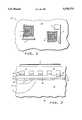
- FIG. 1is a simplified partial top view of an electronic device including integrated copper inductors
- FIG. 2is a simplified partial cross section of a portion of the electronic device of FIG. 1, further including a protective layer.
- plated copperis used to form an integrated inductor which overlies other active components of the overall circuit.
- Plated copperis particularly advantageous relative to the aluminum and gold employed in,the past because aluminum and gold thicknesses are practically limited to around 3 ⁇ m, while copper may easily be pleated to much greater thicknesses.
- the thick plated copper structureprovides much lower resistivity relative to materials employed in the past. The lower resistivity translates to greatly reduced, and therefore improved, series resistance for the integrated inductor.
- the series resistancecan be reduced from 68 ohms for a 1 ⁇ m thick aluminum inductor, to 1.7 ohms for a 20 ⁇ m copper inductor.
- inductorsare plated over a relatively thick dielectric layer above the top layer of circuit metallization of the electronic device.
- the dielectric layerminimizes the parasitics associated with underlying electronic devices. More particularly, a thicker dielectric layer is preferred in order to lower the capacitive coupling between the inductor and underlying devices.
- the copper thicknesshas some latitude, and can be optimized taking into account manufacturability issues such as the dependence on thickness of the photoresist during plating, and the ability to achieve the desired line thickness and spacing. Accordingly, there is some trade-off between minimizing spacing and maximizing thickness to achieve high inductance per area, and low series resistance. This trade-off will depend upon the particular application.
- an inductorIn copper plating, line height to width aspect ratios greater than one have been achieved. For example, given a 1:1 aspect ratio, an inductor could be designed requiring an area of 470 ⁇ m ⁇ 470 ⁇ m, equaling 220,900 ⁇ m 2 . To obtain the same inductance value with a 2:1 aspect ratio, an area of only 300 ⁇ m ⁇ 300 ⁇ m, equaling 90,000 ⁇ m 2 would be required, resulting in a savings of 130,900 ⁇ m 2 . For this discussed example, the inductance per area values are 95 ⁇ 10 -6 (nH/ ⁇ m 2 ) for a 1:1 aspect ratio, and 233 ⁇ 10 -6 (nH/ ⁇ m 2 ) for a 2:1 aspect ratio. The advantage of this approach is the capability to develop integrated circuits having integrated inductors that have lower parasitic capacitance to the substrate, lower series resistance, and higher inductance per unit area.
- FIG. 1is a simplified top view of a portion of an electronic device 10.
- Electronic device 10may, for example, be a voltage controlled oscillator (VCO).
- Electronic device 10includes copper integrated inductors 11 and 12.
- inductors 11 and 12are spiral inductors, but it will be recognized that other configurations could be suitable.
- Inductors 11 and 12overlie the surface 15 of device 10.
- Inductors 11 and 12are connected to electronic device portion 10 at two ports, typically at respective ends of the spiral. According to the embodiment illustrated, one port is connected through copper interconnect 13, which also overlies surface 15, and therefore is in the same plane as inductors 11 and 12. Referring briefly to FIG. 2, another port is connected through via 42, the via 42 extending from inductor 11 to buried interconnect layer 37. Buried interconnect layer 37, lying below surface 15, is used to couple underlying circuitry, as necessary to inductor 11.
- inductor 12 of device 10being contacted externally via contact pad 14. More specifically, contact pad 14 is coupled to copper interconnect 13, in the same plane as surface 15 of device 10. Contact Dad 14 is then available for external connection via for example, wire bonding. Other methods of coupling to the ports of inductor 11 and 12 will of course be recognized by those skilled in the art.
- FIG. 2is a-simplified partial cross-sectional view of a portion of inductor 11, taken at 2--2 shown in FIG. 1. Additionally, FIG. 2 further includes protective layer 41, discussed in more detail below.
- FIG. 2illustrates electronic device portion 30 which is a portion of the entire device 10. Electronic device portion 30 is formed in and on semiconductor substrate 47 according to well known semiconductor processing methods. Electronic device portion 30 includes P-type region 33 and shallow N-type region 32. Together, regions 32 and 33 form a solid state device, more particularly, a diode, 31, where N-type region 32 contacts P-type region 33.
- diode 31may be electrically coupled to other components of the electronic device, including inductor 11, via contact portion 51 of buried interconnect layer 37.
- Portion 51provides convenient connection to N-type region 32 of diode 31. Similar connections, not shown, may be made to P-type region 33 of diode 31.
- dielectric layer 39is formed.
- a suitable material and thicknessis SiO 2 of about 5000 ⁇ .
- dielectric layer 39is deposited with chemical vapor deposition techniques, however, it will be recognized that a variety of techniques are available for forming such a dielectric layer.
- layer 39is patterned and etched with well known processing methods in order to configure layer 39 for the particular application. For example, a via is opened to permit access from buried interconnect layer 37 to diode 31.
- interconnect layer 37comprises aluminum and is deposited using sputter depositions. It will be recognized that other methods of forming interconnect layer 37 are available. Interconnect layer 37 is patterned as necessary for any particular application with well known photolithographic techniques. Interconnect layer 37 provides connections to various active and passive devices comprising the overall electronic device.
- a second dielectric layer 34is deposited above metal interconnect layer 37.
- a suitable materialis polyimide, having a thickness of 1 ⁇ m or greater. According to the preferred embodiment, well known spin-on techniques are used for applying dielectric layer 34.
- via 42is opened in layer 34 using well known photolithographic and etch techniques. Via 42 exposes interconnect layer 37, providing access for inductor 11 to interconnect layer 37, and thereby to diode 31.
- dielectric layer 34should be greater than 1 ⁇ m.
- a layer of metal 43is formed above second dielectric layer 34. It will be understood, that as initially formed, layer 43 entirely covers the upper surface of the structure including any upper surfaces exposed by vias such as Via 42.
- layer 43comprises titanium tungsten (TiW). A suitable thickness is about 500 ⁇ . As will be recognized by those skilled in the art, TiW is used to provide adhesion and to provide a copper diffusion barrier. According to the preferred embodiment, TiW layer 43 is sputter deposited, contacting interconnect layer 37 at the base of via 42.
- a sputtered copper layer 44is deposited above TiW layer 43 to provide adhesion and a surface for plating the remainder of the copper comprising the inductors.
- a suitable thicknessis about 1000 521 . It will be understood that many other metals and alloys may be employed in place of layers 43 and 44.
- Layer 44is also deposited as a complete, unpatterned layer.
- the structureis coated with photoresist (not shown).
- the thickness of the photoresistmay be optimized to provide desired thicknesses for the line widths of inductor 11, depending upon the application. Examples of preferred thicknesses, line widths and inductor configurations are presented earlier in this specification, with accompanying Tables. Furthermore, well known methods for optimization are available for achieving the configurations and geometries discussed in detail and shown in the Tables in the preceding discussion.
- the photoresistis aligned, exposed, and developed, creating a pattern which defines the spiral inductor 11.
- the patterned photoresistis used as a mask during the copper plating process, as is well known in the art.
- a relatively thick layer of plated copper 45is subsequently electroplated on layer 44 which overlies the surface of the substrate.
- the substrateis used as a cathode during the electroplating process. It will be recognized that the copper plates only where photoresist has been removed. Consequently, the copper is plated in the desired pattern, as defined by the photoresist, resulting in inductor 11.
- the photoresist used to define the pattern of the copperis removed, thereby exposing sputtered copper layer 44 between the lines of plated copper 45 that form inductor 11. Sputtered copper layer 44 is subsequently etched exposing TiW layer 43 which is then removed as well.
- plated copper layer 45acts as an etch protect for the portions of sputtered copper Layer 44 and TiW layer 43 which underlie plated copper layer 45.
- Plated copper layer 45is preferably more than ten times the thickness of sputtered copper layer 44. Consequently, etches well known in the industry that are capable of etching both plated and sputtered copper may be employed to etch down through sputtered copper layer 44 to achieve the spiral pattern of the inductor.
- designerswill readily be able to take into account the loss of a small portion of layer 45 during the etch of layer 44.
- an etching methodmay be employed which etches sputtered copper as fast or faster than plated copper.
- a methodis disclosed in U.S. Pat. No. 5,409,567 which issued to Lytle, et al. on Apr. 25, 1995 and assigned to the same assignee, Motorola, Inc.
- the top surface of plated copper layer 45may be protected by an additional overlying layer of metal, for example, tin. The additional metal layer is applied before removing the photoresist which covers sputtered copper layer 44.
- TiW layer 43is etched after layer 44 is etched, thus completing the pattern of inductor 11.
- an encapsulating material 41may be deposited to provide physical and environmental protection for inductor 11 and all other components of electronic device 10.
- Preferred encapsulating materialsinclude molding compound and polyimide.
- the thick plated copper, narrow line widths and narrow spacing used in the preferred embodiment to make small area spiral inductorsprovide extremely low series resistance and good mutual inductance coupling for high inductance values.
- High inductance per area and low series resistanceresults in integrated inductors with high Q values.
- Combining such integrated inductors on the same substrate with passive and/or active components making up the overall electronic deviceeliminates the need for extensive external interfaces which would be required if the inductors were not integrated. Resulting devices in accordance with the preferred embodiment of the present invention provide reduced system size, reduced parasitics, improved quality, lower power requirements and lower costs.
Landscapes
- Physics & Mathematics (AREA)
- Condensed Matter Physics & Semiconductors (AREA)
- General Physics & Mathematics (AREA)
- Engineering & Computer Science (AREA)
- Computer Hardware Design (AREA)
- Microelectronics & Electronic Packaging (AREA)
- Power Engineering (AREA)
- Semiconductor Integrated Circuits (AREA)
Abstract
Description
______________________________________ THICKNESS (μm) 1 3 10 20 ______________________________________ Aluminum 3.4 1.1 -- --Copper 2 0.7 0.2 0.1 DC Resistance (Ohms) ______________________________________
______________________________________ THICKNESS (μm) 1 3 10 20 ______________________________________ Aluminum 68 23 -- --Copper 34 11 3.4 1.7 DC Resistance (Ohms) ______________________________________
Claims (17)
Priority Applications (1)
| Application Number | Priority Date | Filing Date | Title |
|---|---|---|---|
| US08/451,866US5478773A (en) | 1994-04-28 | 1995-05-26 | Method of making an electronic device having an integrated inductor |
Applications Claiming Priority (2)
| Application Number | Priority Date | Filing Date | Title |
|---|---|---|---|
| US23420394A | 1994-04-28 | 1994-04-28 | |
| US08/451,866US5478773A (en) | 1994-04-28 | 1995-05-26 | Method of making an electronic device having an integrated inductor |
Related Parent Applications (1)
| Application Number | Title | Priority Date | Filing Date |
|---|---|---|---|
| US23420394ADivision | 1994-04-28 | 1994-04-28 |
Publications (1)
| Publication Number | Publication Date |
|---|---|
| US5478773Atrue US5478773A (en) | 1995-12-26 |
Family
ID=22880376
Family Applications (1)
| Application Number | Title | Priority Date | Filing Date |
|---|---|---|---|
| US08/451,866Expired - LifetimeUS5478773A (en) | 1994-04-28 | 1995-05-26 | Method of making an electronic device having an integrated inductor |
Country Status (1)
| Country | Link |
|---|---|
| US (1) | US5478773A (en) |
Cited By (76)
| Publication number | Priority date | Publication date | Assignee | Title |
|---|---|---|---|---|
| US5985125A (en)* | 1995-07-24 | 1999-11-16 | Lg Semicon Co., Ltd. | Selective copper deposition method |
| US6008102A (en)* | 1998-04-09 | 1999-12-28 | Motorola, Inc. | Method of forming a three-dimensional integrated inductor |
| US6013939A (en)* | 1997-10-31 | 2000-01-11 | National Scientific Corp. | Monolithic inductor with magnetic flux lines guided away from substrate |
| US6030877A (en)* | 1997-10-06 | 2000-02-29 | Industrial Technology Research Institute | Electroless gold plating method for forming inductor structures |
| WO2000007218A3 (en)* | 1998-07-28 | 2000-05-04 | Korea Advanced Inst Sci & Tech | Method for manufacturing a semiconductor device having a metal layer floating over a substrate |
| EP1017102A1 (en)* | 1998-12-29 | 2000-07-05 | Koninklijke Philips Electronics N.V. | Integrated circuit comprising inductive elements |
| EP1039544A1 (en)* | 1999-03-23 | 2000-09-27 | Memscap | Monolithic integrated circuit comprising an inductor and a method of fabricating the same |
| US6160303A (en)* | 1997-08-29 | 2000-12-12 | Texas Instruments Incorporated | Monolithic inductor with guard rings |
| WO2001004953A1 (en)* | 1999-07-08 | 2001-01-18 | Korea Advanced Institute Of Science And Technology | Method for manufacturing a semiconductor device having a metal layer floating over a substrate |
| US6236101B1 (en)* | 1997-11-05 | 2001-05-22 | Texas Instruments Incorporated | Metallization outside protective overcoat for improved capacitors and inductors |
| US6387747B1 (en) | 2001-05-31 | 2002-05-14 | Chartered Semiconductor Manufacturing Ltd. | Method to fabricate RF inductors with minimum area |
| US6404615B1 (en) | 2000-02-16 | 2002-06-11 | Intarsia Corporation | Thin film capacitors |
| US6469609B2 (en) | 2000-01-28 | 2002-10-22 | Electronics And Telecommunications Research Institute | Method of fabricating silver inductor |
| US6486530B1 (en) | 2000-10-16 | 2002-11-26 | Intarsia Corporation | Integration of anodized metal capacitors and high temperature deposition capacitors |
| US6636139B2 (en) | 2001-09-10 | 2003-10-21 | Taiwan Semiconductor Manufacturing Company | Structure to reduce the degradation of the Q value of an inductor caused by via resistance |
| US20030222295A1 (en)* | 1998-12-21 | 2003-12-04 | Megic Corporation | High performance system-on-chip inductor using post passivation process |
| US6700177B2 (en)* | 2000-05-30 | 2004-03-02 | Alps Electric Co., Ltd. | Compact, surface-mounting-type, electronic-circuit unit |
| US6714113B1 (en) | 2000-11-14 | 2004-03-30 | International Business Machines Corporation | Inductor for integrated circuits |
| US20040104449A1 (en)* | 2001-03-29 | 2004-06-03 | Jun-Bo Yoon | Three- dimensional metal devices highly suspended above semiconductor substrate, their circuit model, and method for manufacturing the same |
| US20040121606A1 (en)* | 2002-12-23 | 2004-06-24 | Motorola, Inc. | Flip-chip structure and method for high quality inductors and transformers |
| US6759746B1 (en) | 2000-03-17 | 2004-07-06 | Robert Bruce Davies | Die attachment and method |
| US20050065545A1 (en)* | 2003-09-23 | 2005-03-24 | Scimed Life Systems, Inc. | External activation of vaso-occlusive implants |
| US20050104177A1 (en)* | 2000-10-18 | 2005-05-19 | Megic Corporation | Post passivation interconnection schemes on top of the IC chips |
| US20050160575A1 (en)* | 2004-01-22 | 2005-07-28 | International Business Machines Corporation | Integration of high performance copper inductors with bond pads |
| US20060022311A1 (en)* | 2003-05-08 | 2006-02-02 | Mou-Shiung Lin | Chip structure with redistribution Circuit, chip package and manufacturing process thereof |
| US20060038289A1 (en)* | 2004-04-26 | 2006-02-23 | Rockwell Hsu | Integrated inductors and compliant interconnects for semiconductor packaging |
| US20060040628A1 (en)* | 2004-08-20 | 2006-02-23 | Alain-Serge Porret | Television receiver including an integrated band selection filter |
| US20060063378A1 (en)* | 2004-09-23 | 2006-03-23 | Megie Corporation | Top layers of metal for integrated circuits |
| US20060060973A1 (en)* | 2000-10-18 | 2006-03-23 | Megic Corporation | Post passivation interconnection schemes on top of the IC chips |
| US20060170527A1 (en)* | 2005-02-02 | 2006-08-03 | Henning Braunisch | Integrated transformer structure and method of fabrication |
| US20070108551A1 (en)* | 2003-05-27 | 2007-05-17 | Megica Corporation | High performance system-on-chip inductor using post passivation process |
| US20070114651A1 (en)* | 2005-10-29 | 2007-05-24 | Stats Chippac Ltd. | Integrated circuit stacking system with integrated passive components |
| US20070114634A1 (en)* | 2005-10-29 | 2007-05-24 | Stats Chippac Ltd. | Integrated passive device system |
| US20070138572A1 (en)* | 2005-12-15 | 2007-06-21 | Atmel Corporation | An electronics package with an integrated circuit device having post wafer fabrication integrated passive components |
| US20070139066A1 (en)* | 2005-12-19 | 2007-06-21 | Silicon Laboratories Inc. | Integrated current sensor package |
| US20070200244A1 (en)* | 2003-10-15 | 2007-08-30 | Mou-Shiung Lin | Post passivation interconnection schemes on top of the IC chips |
| US7271489B2 (en) | 2003-10-15 | 2007-09-18 | Megica Corporation | Post passivation interconnection schemes on top of the IC chips |
| US20070284751A1 (en)* | 1998-12-21 | 2007-12-13 | Mou-Shiung Lin | Top layers of metal for high performance IC's |
| US20070284726A1 (en)* | 2006-03-30 | 2007-12-13 | Yaojian Lin | Integrated circuit package system with post-passivation interconnection and integration |
| US20080038869A1 (en)* | 1998-12-21 | 2008-02-14 | Megica Corporation | High performance system-on-chip using post passivation process |
| US20080054428A1 (en)* | 2006-07-13 | 2008-03-06 | Atmel Corporation | A stacked-die electronics package with planar and three-dimensional inductor elements |
| US20080057658A1 (en)* | 2006-09-06 | 2008-03-06 | Atmel Corporation | Method for fabricating a thick copper line and copper inductor resulting therefrom |
| US20080128910A1 (en)* | 2004-09-09 | 2008-06-05 | Megica Corporation | Post Passivation Interconnection Process And Structures |
| US20080150623A1 (en)* | 2006-12-26 | 2008-06-26 | Megica Corporation | Voltage Regulator Integrated with Semiconductor Chip |
| US20080233731A1 (en)* | 2007-03-21 | 2008-09-25 | Stats Chippac, Ltd. | Method of Forming Top Electrode for Capacitor and Interconnection in Integrated Passive Device (IPD) |
| US20080277759A1 (en)* | 2005-07-27 | 2008-11-13 | Anil Kumar Chinthakindi | Post last wiring level inductor using patterned plate process |
| US20080290520A1 (en)* | 2004-09-09 | 2008-11-27 | Megica Corporation | Reliable metal bumps on top of I/O pads after removal of test probe marks |
| US20090001962A1 (en)* | 2006-06-30 | 2009-01-01 | Dupuis Timothy J | Current sensor with reset circuit |
| US20090001511A1 (en)* | 2005-03-29 | 2009-01-01 | Megica Corporation | High performance system-on-chip using post passivation process |
| US20090065871A1 (en)* | 2005-09-23 | 2009-03-12 | Megica Corporation | Semiconductor chip and process for forming the same |
| US20090104769A1 (en)* | 2005-05-18 | 2009-04-23 | Megica Corporation | Semiconductor chip with coil element over passivation layer |
| US20090146305A1 (en)* | 2004-10-12 | 2009-06-11 | Megica Corporation | Post passivation interconnection schemes on top of the ic chips |
| US20090284248A1 (en)* | 2008-05-15 | 2009-11-19 | Etter Brett E | Method and apparatus for high current measurement |
| US20090294957A1 (en)* | 2005-12-15 | 2009-12-03 | Lam Ken M | Apparatus and method for increasing the quantity of discrete electronic components in an integrated circuit package |
| US20100165585A1 (en)* | 2008-12-26 | 2010-07-01 | Megica Corporation | Chip packages with power management integrated circuits and related techniques |
| US20100171194A1 (en)* | 2005-10-29 | 2010-07-08 | Stats Chippac, Ltd. | Semiconductor Device and Method of Forming an Inductor on Polymer Matrix Composite Substrate |
| USRE41581E1 (en) | 1999-07-12 | 2010-08-24 | Robert Bruce Davies | Monolithic low dielectric constant platform for passive components and method |
| US20100264516A1 (en)* | 2007-11-07 | 2010-10-21 | Stats Chippac, Ltd. | Method of Forming an Inductor on a Semiconductor Wafer |
| US7855461B2 (en) | 2003-12-08 | 2010-12-21 | Megica Corporation | Chip structure with bumps and testing pads |
| US7898058B2 (en) | 2001-12-31 | 2011-03-01 | Megica Corporation | Integrated chip package structure using organic substrate and method of manufacturing the same |
| US7960269B2 (en) | 2005-07-22 | 2011-06-14 | Megica Corporation | Method for forming a double embossing structure |
| US7973629B2 (en) | 2001-09-04 | 2011-07-05 | Megica Corporation | Method for making high-performance RF integrated circuits |
| US8008775B2 (en) | 2004-09-09 | 2011-08-30 | Megica Corporation | Post passivation interconnection structures |
| US8089155B2 (en) | 1998-12-21 | 2012-01-03 | Megica Corporation | High performance system-on-chip discrete components using post passivation process |
| US8212155B1 (en)* | 2007-06-26 | 2012-07-03 | Wright Peter V | Integrated passive device |
| US8421158B2 (en) | 1998-12-21 | 2013-04-16 | Megica Corporation | Chip structure with a passive device and method for forming the same |
| US8492870B2 (en) | 2002-01-19 | 2013-07-23 | Megica Corporation | Semiconductor package with interconnect layers |
| US8535976B2 (en) | 2001-12-31 | 2013-09-17 | Megica Corporation | Method for fabricating chip package with die and substrate |
| US8558344B2 (en) | 2011-09-06 | 2013-10-15 | Analog Devices, Inc. | Small size and fully integrated power converter with magnetics on chip |
| US8786393B1 (en) | 2013-02-05 | 2014-07-22 | Analog Devices, Inc. | Step up or step down micro-transformer with tight magnetic coupling |
| US20140253279A1 (en)* | 2013-03-08 | 2014-09-11 | Qualcomm Incorporated | Coupled discrete inductor with flux concentration using high permeable material |
| US9030029B2 (en) | 2001-12-31 | 2015-05-12 | Qualcomm Incorporated | Chip package with die and substrate |
| US9293997B2 (en) | 2013-03-14 | 2016-03-22 | Analog Devices Global | Isolated error amplifier for isolated power supplies |
| US20160126925A1 (en)* | 2014-11-03 | 2016-05-05 | Rf Micro Devices, Inc. | Semiconductor resonators with reduced substrate losses |
| US9449925B2 (en) | 2005-10-29 | 2016-09-20 | STATS ChipPAC Pte. Ltd. | Integrated passive devices |
| US9685495B2 (en) | 2009-11-19 | 2017-06-20 | STATS ChipPAC, Pte. Ltd. | Semiconductor device and method of forming IPD on molded substrate |
Citations (9)
| Publication number | Priority date | Publication date | Assignee | Title |
|---|---|---|---|---|
| US3305814A (en)* | 1967-02-21 | Hybrid solid state device | ||
| US4785345A (en)* | 1986-05-08 | 1988-11-15 | American Telephone And Telegraph Co., At&T Bell Labs. | Integrated transformer structure with primary winding in substrate |
| GB2211987A (en)* | 1987-10-30 | 1989-07-12 | Plessey Co Plc | Circuit arrangement of inductor and MESFET |
| US5070317A (en)* | 1989-01-17 | 1991-12-03 | Bhagat Jayant K | Miniature inductor for integrated circuits and devices |
| US5095357A (en)* | 1989-08-18 | 1992-03-10 | Mitsubishi Denki Kabushiki Kaisha | Inductive structures for semiconductor integrated circuits |
| US5111169A (en)* | 1989-03-23 | 1992-05-05 | Takeshi Ikeda | Lc noise filter |
| US5174012A (en)* | 1989-11-27 | 1992-12-29 | Censtor Corp. | Method of making magnetic read/write head/flexure/conductor unit(s) |
| GB2269935A (en)* | 1992-07-21 | 1994-02-23 | Mitsubishi Electric Corp | Compact semiconductor device with moulded body |
| US5384274A (en)* | 1992-04-06 | 1995-01-24 | Nippon Precision Circuits Inc. | Method of making a combined semiconductor device and inductor |
- 1995
- 1995-05-26USUS08/451,866patent/US5478773A/ennot_activeExpired - Lifetime
Patent Citations (9)
| Publication number | Priority date | Publication date | Assignee | Title |
|---|---|---|---|---|
| US3305814A (en)* | 1967-02-21 | Hybrid solid state device | ||
| US4785345A (en)* | 1986-05-08 | 1988-11-15 | American Telephone And Telegraph Co., At&T Bell Labs. | Integrated transformer structure with primary winding in substrate |
| GB2211987A (en)* | 1987-10-30 | 1989-07-12 | Plessey Co Plc | Circuit arrangement of inductor and MESFET |
| US5070317A (en)* | 1989-01-17 | 1991-12-03 | Bhagat Jayant K | Miniature inductor for integrated circuits and devices |
| US5111169A (en)* | 1989-03-23 | 1992-05-05 | Takeshi Ikeda | Lc noise filter |
| US5095357A (en)* | 1989-08-18 | 1992-03-10 | Mitsubishi Denki Kabushiki Kaisha | Inductive structures for semiconductor integrated circuits |
| US5174012A (en)* | 1989-11-27 | 1992-12-29 | Censtor Corp. | Method of making magnetic read/write head/flexure/conductor unit(s) |
| US5384274A (en)* | 1992-04-06 | 1995-01-24 | Nippon Precision Circuits Inc. | Method of making a combined semiconductor device and inductor |
| GB2269935A (en)* | 1992-07-21 | 1994-02-23 | Mitsubishi Electric Corp | Compact semiconductor device with moulded body |
Cited By (204)
| Publication number | Priority date | Publication date | Assignee | Title |
|---|---|---|---|---|
| US5985125A (en)* | 1995-07-24 | 1999-11-16 | Lg Semicon Co., Ltd. | Selective copper deposition method |
| US6160303A (en)* | 1997-08-29 | 2000-12-12 | Texas Instruments Incorporated | Monolithic inductor with guard rings |
| US6030877A (en)* | 1997-10-06 | 2000-02-29 | Industrial Technology Research Institute | Electroless gold plating method for forming inductor structures |
| US6013939A (en)* | 1997-10-31 | 2000-01-11 | National Scientific Corp. | Monolithic inductor with magnetic flux lines guided away from substrate |
| US6281778B1 (en) | 1997-10-31 | 2001-08-28 | National Scientific Corp. | Monolithic inductor with magnetic flux lines guided away from substrate |
| US6236101B1 (en)* | 1997-11-05 | 2001-05-22 | Texas Instruments Incorporated | Metallization outside protective overcoat for improved capacitors and inductors |
| US6008102A (en)* | 1998-04-09 | 1999-12-28 | Motorola, Inc. | Method of forming a three-dimensional integrated inductor |
| WO2000007218A3 (en)* | 1998-07-28 | 2000-05-04 | Korea Advanced Inst Sci & Tech | Method for manufacturing a semiconductor device having a metal layer floating over a substrate |
| US6518165B1 (en) | 1998-07-28 | 2003-02-11 | Korea Advanced Institute Of Science And Technology | Method for manufacturing a semiconductor device having a metal layer floating over a substrate |
| US20080042273A1 (en)* | 1998-12-21 | 2008-02-21 | Megica Corporation | High performance system-on-chip using post passivation process |
| US8129265B2 (en) | 1998-12-21 | 2012-03-06 | Megica Corporation | High performance system-on-chip discrete components using post passivation process |
| US20070181970A1 (en)* | 1998-12-21 | 2007-08-09 | Megica Corporation | High performance system-on-chip inductor using post passivation process |
| US8487400B2 (en) | 1998-12-21 | 2013-07-16 | Megica Corporation | High performance system-on-chip using post passivation process |
| US8421158B2 (en) | 1998-12-21 | 2013-04-16 | Megica Corporation | Chip structure with a passive device and method for forming the same |
| US8415800B2 (en) | 1998-12-21 | 2013-04-09 | Megica Corporation | Top layers of metal for high performance IC's |
| US8531038B2 (en) | 1998-12-21 | 2013-09-10 | Megica Corporation | Top layers of metal for high performance IC's |
| US20070284751A1 (en)* | 1998-12-21 | 2007-12-13 | Mou-Shiung Lin | Top layers of metal for high performance IC's |
| US20070284752A1 (en)* | 1998-12-21 | 2007-12-13 | Mou-Shiung Lin | Top layers of metal for high performance IC's |
| US7863654B2 (en) | 1998-12-21 | 2011-01-04 | Megica Corporation | Top layers of metal for high performance IC's |
| US20030222295A1 (en)* | 1998-12-21 | 2003-12-04 | Megic Corporation | High performance system-on-chip inductor using post passivation process |
| US20070284753A1 (en)* | 1998-12-21 | 2007-12-13 | Mou-Shiung Lin | Top layers of metal for high performance IC's |
| US7884479B2 (en) | 1998-12-21 | 2011-02-08 | Megica Corporation | Top layers of metal for high performance IC's |
| US7999384B2 (en) | 1998-12-21 | 2011-08-16 | Megica Corporation | Top layers of metal for high performance IC's |
| US8022545B2 (en) | 1998-12-21 | 2011-09-20 | Megica Corporation | Top layers of metal for high performance IC's |
| US20080038869A1 (en)* | 1998-12-21 | 2008-02-14 | Megica Corporation | High performance system-on-chip using post passivation process |
| US8089155B2 (en) | 1998-12-21 | 2012-01-03 | Megica Corporation | High performance system-on-chip discrete components using post passivation process |
| US20080035972A1 (en)* | 1998-12-21 | 2008-02-14 | Megica Corporation | High performance system-on-chip using post passivation process |
| US8178435B2 (en)* | 1998-12-21 | 2012-05-15 | Megica Corporation | High performance system-on-chip inductor using post passivation process |
| US8304907B2 (en) | 1998-12-21 | 2012-11-06 | Megica Corporation | Top layers of metal for integrated circuits |
| US8471384B2 (en) | 1998-12-21 | 2013-06-25 | Megica Corporation | Top layers of metal for high performance IC's |
| EP1017102A1 (en)* | 1998-12-29 | 2000-07-05 | Koninklijke Philips Electronics N.V. | Integrated circuit comprising inductive elements |
| US6548365B2 (en)* | 1999-03-23 | 2003-04-15 | Memscap S.A. And Planhead-Silmag Phs, S.A. | Monolithic integrated circuit incorporating an inductive component and process for fabricating such an integrated circuit |
| EP1039544A1 (en)* | 1999-03-23 | 2000-09-27 | Memscap | Monolithic integrated circuit comprising an inductor and a method of fabricating the same |
| US6459135B1 (en)* | 1999-03-23 | 2002-10-01 | Memscap S.A. | Monolithic integrated circuit incorporating an inductive component and process for fabricating such an integrated circuit |
| WO2001004953A1 (en)* | 1999-07-08 | 2001-01-18 | Korea Advanced Institute Of Science And Technology | Method for manufacturing a semiconductor device having a metal layer floating over a substrate |
| USRE41581E1 (en) | 1999-07-12 | 2010-08-24 | Robert Bruce Davies | Monolithic low dielectric constant platform for passive components and method |
| US6469609B2 (en) | 2000-01-28 | 2002-10-22 | Electronics And Telecommunications Research Institute | Method of fabricating silver inductor |
| US6404615B1 (en) | 2000-02-16 | 2002-06-11 | Intarsia Corporation | Thin film capacitors |
| US6759746B1 (en) | 2000-03-17 | 2004-07-06 | Robert Bruce Davies | Die attachment and method |
| EP1160869A3 (en)* | 2000-05-30 | 2006-01-25 | Alps Electric Co., Ltd. | SMD with passive components formed by thin film technology |
| US6700177B2 (en)* | 2000-05-30 | 2004-03-02 | Alps Electric Co., Ltd. | Compact, surface-mounting-type, electronic-circuit unit |
| US6486530B1 (en) | 2000-10-16 | 2002-11-26 | Intarsia Corporation | Integration of anodized metal capacitors and high temperature deposition capacitors |
| US20080085596A1 (en)* | 2000-10-18 | 2008-04-10 | Megica Corporation | Post passivation interconnection schemes on top of IC chips |
| US20080042293A1 (en)* | 2000-10-18 | 2008-02-21 | Megica Corporation | Post passivation interconnection schemes on top of IC chip |
| US8482127B2 (en) | 2000-10-18 | 2013-07-09 | Megica Corporation | Post passivation interconnection schemes on top of IC chip |
| US7524759B2 (en) | 2000-10-18 | 2009-04-28 | Megica Corporation | Post passivation interconnection schemes on top of IC chip |
| US7479450B2 (en) | 2000-10-18 | 2009-01-20 | Megica Corporation | Post passivation interconnection schemes on top of the IC chips |
| US8461686B2 (en) | 2000-10-18 | 2013-06-11 | Megica Corporation | Post passivation interconnection schemes on top of IC chip |
| US7892965B2 (en) | 2000-10-18 | 2011-02-22 | Megica Corporation | Post passivation interconnection schemes on top of IC chip |
| US7265047B2 (en) | 2000-10-18 | 2007-09-04 | Megica Corporation | Post passivation interconnection schemes on top of the IC chips |
| US7466007B2 (en) | 2000-10-18 | 2008-12-16 | Megica Corporation | Post passivation interconnection schemes on top of IC chip |
| US7276422B2 (en) | 2000-10-18 | 2007-10-02 | Megica Corporation | Post passivation interconnection schemes on top of the IC chips |
| US8435883B2 (en) | 2000-10-18 | 2013-05-07 | Megica Corporation | Post passivation interconnection schemes on top of IC chips |
| US7462938B2 (en) | 2000-10-18 | 2008-12-09 | Megica Corporation | Post passivation interconnection schemes on top of IC chip |
| US8492900B2 (en) | 2000-10-18 | 2013-07-23 | Megica Corporation | Post passivation interconnection schemes on top of IC chip |
| US20060076684A1 (en)* | 2000-10-18 | 2006-04-13 | Megic Corporation | Post passivation interconnection schemes on top of the IC chips |
| US20060060973A1 (en)* | 2000-10-18 | 2006-03-23 | Megic Corporation | Post passivation interconnection schemes on top of the IC chips |
| US7459791B2 (en) | 2000-10-18 | 2008-12-02 | Megica Corporation | Post passivation interconnection schemes on top of IC chip |
| US7902067B2 (en) | 2000-10-18 | 2011-03-08 | Megica Corporation | Post passivation interconnection schemes on top of the IC chips |
| US20080001301A1 (en)* | 2000-10-18 | 2008-01-03 | Megica Corporation | Post passivation interconnection schemes on top of IC chip |
| US20080001294A1 (en)* | 2000-10-18 | 2008-01-03 | Megica Corporation | Post passivation interconnection schemes on top of IC chip |
| US20080001293A1 (en)* | 2000-10-18 | 2008-01-03 | Megica Corporation | Post passivation interconnection schemes on top of IC chip |
| US20080001302A1 (en)* | 2000-10-18 | 2008-01-03 | Megica Corporation | Post passivation interconnection schemes on top of IC chip |
| US20080003806A1 (en)* | 2000-10-18 | 2008-01-03 | Megica Corporation | Post passivation interconnection schemes on top of IC chip |
| US20080006946A1 (en)* | 2000-10-18 | 2008-01-10 | Megica Corporation | Post passivation interconnection schemes on top of the ic chips |
| US20080009131A1 (en)* | 2000-10-18 | 2008-01-10 | Megica Corporation | Post passivation interconnection schemes on top of the ic chips |
| US7915161B2 (en) | 2000-10-18 | 2011-03-29 | Megica Corporation | Post passivation interconnection schemes on top of IC chip |
| US7919865B2 (en) | 2000-10-18 | 2011-04-05 | Megica Corporation | Post passivation interconnection schemes on top of IC chip |
| US7923366B2 (en) | 2000-10-18 | 2011-04-12 | Megica Corporation | Post passivation interconnection schemes on top of IC chip |
| US20080045001A1 (en)* | 2000-10-18 | 2008-02-21 | Megica Corporation | Post passivation interconnection schemes on top of IC chip |
| US20080042295A1 (en)* | 2000-10-18 | 2008-02-21 | Megica Corporation | Post passivation interconnection schemes on top of IC chip |
| US20080045008A1 (en)* | 2000-10-18 | 2008-02-21 | Megica Corporation | Post passivation interconnection schemes on top of IC chip |
| US20080045004A1 (en)* | 2000-10-18 | 2008-02-21 | Megica Corporation | Post passivation interconnection schemes on top of IC chips |
| US7446035B2 (en) | 2000-10-18 | 2008-11-04 | Megica Corporation | Post passivation interconnection schemes on top of IC chips |
| US20080042285A1 (en)* | 2000-10-18 | 2008-02-21 | Megica Corporation | Post passivation interconnection schemes on top of IC chip |
| US7446031B2 (en) | 2000-10-18 | 2008-11-04 | Megica Corporation | Post passivation interconnection schemes on top of IC chips |
| US20080057703A1 (en)* | 2000-10-18 | 2008-03-06 | Megica Corporation | Post passivation interconnection schemes on top of IC chip |
| US7439626B2 (en) | 2000-10-18 | 2008-10-21 | Megica Corporation | Post passivation interconnection schemes on top of IC chip |
| US8188603B2 (en) | 2000-10-18 | 2012-05-29 | Megica Corporation | Post passivation interconnection schemes on top of IC chip |
| US20080067693A1 (en)* | 2000-10-18 | 2008-03-20 | Megica Corporation | Post passivation interconnection schemes on top of IC chip |
| US20080085597A1 (en)* | 2000-10-18 | 2008-04-10 | Megica Corporation | Post passivation interconnection schemes on top of IC chips |
| US7534718B2 (en) | 2000-10-18 | 2009-05-19 | Megica Corporation | Post passivation interconnection schemes on top of IC chips |
| US7372161B2 (en) | 2000-10-18 | 2008-05-13 | Megica Corporation | Post passivation interconnection schemes on top of the IC chips |
| US20050104177A1 (en)* | 2000-10-18 | 2005-05-19 | Megic Corporation | Post passivation interconnection schemes on top of the IC chips |
| US7382052B2 (en) | 2000-10-18 | 2008-06-03 | Mou-Shiung Lin | Post passivation interconnection schemes on top of IC chip |
| US7439627B2 (en) | 2000-10-18 | 2008-10-21 | Megica Corporation | Post passivation interconnection schemes on top of the IC chips |
| US8004088B2 (en) | 2000-10-18 | 2011-08-23 | Megica Corporation | Post passivation interconnection schemes on top of IC chip |
| US6714113B1 (en) | 2000-11-14 | 2004-03-30 | International Business Machines Corporation | Inductor for integrated circuits |
| US20040104449A1 (en)* | 2001-03-29 | 2004-06-03 | Jun-Bo Yoon | Three- dimensional metal devices highly suspended above semiconductor substrate, their circuit model, and method for manufacturing the same |
| US6387747B1 (en) | 2001-05-31 | 2002-05-14 | Chartered Semiconductor Manufacturing Ltd. | Method to fabricate RF inductors with minimum area |
| US7973629B2 (en) | 2001-09-04 | 2011-07-05 | Megica Corporation | Method for making high-performance RF integrated circuits |
| US8384508B2 (en) | 2001-09-04 | 2013-02-26 | Megica Corporation | Method for making high-performance RF integrated circuits |
| US6636139B2 (en) | 2001-09-10 | 2003-10-21 | Taiwan Semiconductor Manufacturing Company | Structure to reduce the degradation of the Q value of an inductor caused by via resistance |
| US7898058B2 (en) | 2001-12-31 | 2011-03-01 | Megica Corporation | Integrated chip package structure using organic substrate and method of manufacturing the same |
| US9136246B2 (en) | 2001-12-31 | 2015-09-15 | Qualcomm Incorporated | Integrated chip package structure using silicon substrate and method of manufacturing the same |
| US8471361B2 (en) | 2001-12-31 | 2013-06-25 | Megica Corporation | Integrated chip package structure using organic substrate and method of manufacturing the same |
| US9030029B2 (en) | 2001-12-31 | 2015-05-12 | Qualcomm Incorporated | Chip package with die and substrate |
| US8835221B2 (en) | 2001-12-31 | 2014-09-16 | Qualcomm Incorporated | Integrated chip package structure using ceramic substrate and method of manufacturing the same |
| US8535976B2 (en) | 2001-12-31 | 2013-09-17 | Megica Corporation | Method for fabricating chip package with die and substrate |
| US8492870B2 (en) | 2002-01-19 | 2013-07-23 | Megica Corporation | Semiconductor package with interconnect layers |
| US20040121606A1 (en)* | 2002-12-23 | 2004-06-24 | Motorola, Inc. | Flip-chip structure and method for high quality inductors and transformers |
| US6878633B2 (en) | 2002-12-23 | 2005-04-12 | Freescale Semiconductor, Inc. | Flip-chip structure and method for high quality inductors and transformers |
| US7319277B2 (en) | 2003-05-08 | 2008-01-15 | Megica Corporation | Chip structure with redistribution traces |
| US20060022311A1 (en)* | 2003-05-08 | 2006-02-02 | Mou-Shiung Lin | Chip structure with redistribution Circuit, chip package and manufacturing process thereof |
| US20070108551A1 (en)* | 2003-05-27 | 2007-05-17 | Megica Corporation | High performance system-on-chip inductor using post passivation process |
| US20070202685A1 (en)* | 2003-05-27 | 2007-08-30 | Megica Corporation | High performance system-on-chip inductor using post passivation process |
| US20070202684A1 (en)* | 2003-05-27 | 2007-08-30 | Megica Corporation | High performance system-on-chip inductor using post passivation process |
| US20070182521A1 (en)* | 2003-05-27 | 2007-08-09 | Megica Corporation | High performance system-on-chip inductor using post passivation process |
| US20050065545A1 (en)* | 2003-09-23 | 2005-03-24 | Scimed Life Systems, Inc. | External activation of vaso-occlusive implants |
| US7271489B2 (en) | 2003-10-15 | 2007-09-18 | Megica Corporation | Post passivation interconnection schemes on top of the IC chips |
| US20080116581A1 (en)* | 2003-10-15 | 2008-05-22 | Megica Corporation | Post passivation interconnection schemes on top of the ic chips |
| US7417317B2 (en) | 2003-10-15 | 2008-08-26 | Megica Corporation | Post passivation interconnection schemes on top of the IC chips |
| US8013449B2 (en) | 2003-10-15 | 2011-09-06 | Megica Corporation | Post passivation interconnection schemes on top of the IC chips |
| US7928576B2 (en) | 2003-10-15 | 2011-04-19 | Megica Corporation | Post passivation interconnection schemes on top of the IC chips |
| US7459790B2 (en) | 2003-10-15 | 2008-12-02 | Megica Corporation | Post passivation interconnection schemes on top of the IC chips |
| US20070246834A1 (en)* | 2003-10-15 | 2007-10-25 | Megica Corporation | Post passivation interconnection schemes on top of the IC chips |
| US8456013B2 (en) | 2003-10-15 | 2013-06-04 | Megica Corporation | Post passivation interconnection schemes on top of the IC chips |
| US20070200244A1 (en)* | 2003-10-15 | 2007-08-30 | Mou-Shiung Lin | Post passivation interconnection schemes on top of the IC chips |
| US7855461B2 (en) | 2003-12-08 | 2010-12-21 | Megica Corporation | Chip structure with bumps and testing pads |
| US20050160575A1 (en)* | 2004-01-22 | 2005-07-28 | International Business Machines Corporation | Integration of high performance copper inductors with bond pads |
| US7207096B2 (en) | 2004-01-22 | 2007-04-24 | International Business Machines Corporation | Method of manufacturing high performance copper inductors with bond pads |
| US7279391B2 (en)* | 2004-04-26 | 2007-10-09 | Intel Corporation | Integrated inductors and compliant interconnects for semiconductor packaging |
| US20060038289A1 (en)* | 2004-04-26 | 2006-02-23 | Rockwell Hsu | Integrated inductors and compliant interconnects for semiconductor packaging |
| US7251466B2 (en) | 2004-08-20 | 2007-07-31 | Xceive Corporation | Television receiver including an integrated band selection filter |
| US20060040628A1 (en)* | 2004-08-20 | 2006-02-23 | Alain-Serge Porret | Television receiver including an integrated band selection filter |
| US8008775B2 (en) | 2004-09-09 | 2011-08-30 | Megica Corporation | Post passivation interconnection structures |
| US8018060B2 (en) | 2004-09-09 | 2011-09-13 | Megica Corporation | Post passivation interconnection process and structures |
| US8120181B2 (en) | 2004-09-09 | 2012-02-21 | Megica Corporation | Post passivation interconnection process and structures |
| US20080128910A1 (en)* | 2004-09-09 | 2008-06-05 | Megica Corporation | Post Passivation Interconnection Process And Structures |
| US20080290520A1 (en)* | 2004-09-09 | 2008-11-27 | Megica Corporation | Reliable metal bumps on top of I/O pads after removal of test probe marks |
| US7381642B2 (en) | 2004-09-23 | 2008-06-03 | Megica Corporation | Top layers of metal for integrated circuits |
| US20060063378A1 (en)* | 2004-09-23 | 2006-03-23 | Megie Corporation | Top layers of metal for integrated circuits |
| US7880304B2 (en) | 2004-10-12 | 2011-02-01 | Megica Corporation | Post passivation interconnection schemes on top of the IC chips |
| US20090146305A1 (en)* | 2004-10-12 | 2009-06-11 | Megica Corporation | Post passivation interconnection schemes on top of the ic chips |
| US20060170527A1 (en)* | 2005-02-02 | 2006-08-03 | Henning Braunisch | Integrated transformer structure and method of fabrication |
| US7280024B2 (en)* | 2005-02-02 | 2007-10-09 | Intel Corporation | Integrated transformer structure and method of fabrication |
| US20090001511A1 (en)* | 2005-03-29 | 2009-01-01 | Megica Corporation | High performance system-on-chip using post passivation process |
| US8384189B2 (en) | 2005-03-29 | 2013-02-26 | Megica Corporation | High performance system-on-chip using post passivation process |
| US7985653B2 (en) | 2005-05-18 | 2011-07-26 | Megica Corporation | Semiconductor chip with coil element over passivation layer |
| US8362588B2 (en) | 2005-05-18 | 2013-01-29 | Megica Corporation | Semiconductor chip with coil element over passivation layer |
| US20090104769A1 (en)* | 2005-05-18 | 2009-04-23 | Megica Corporation | Semiconductor chip with coil element over passivation layer |
| US7960269B2 (en) | 2005-07-22 | 2011-06-14 | Megica Corporation | Method for forming a double embossing structure |
| US20080293210A1 (en)* | 2005-07-27 | 2008-11-27 | Anil Kumar Chinthakindi | Post last wiring level inductor using patterned plate process |
| US7763954B2 (en)* | 2005-07-27 | 2010-07-27 | International Business Machines Corporation | Post last wiring level inductor using patterned plate process |
| US7741698B2 (en) | 2005-07-27 | 2010-06-22 | International Business Machines Corporation | Post last wiring level inductor using patterned plate process |
| US7732295B2 (en) | 2005-07-27 | 2010-06-08 | International Business Machines Corporation | Post last wiring level inductor using patterned plate process |
| US20080277759A1 (en)* | 2005-07-27 | 2008-11-13 | Anil Kumar Chinthakindi | Post last wiring level inductor using patterned plate process |
| US7732294B2 (en) | 2005-07-27 | 2010-06-08 | International Business Machines Corporation | Post last wiring level inductor using patterned plate process |
| US20080293233A1 (en)* | 2005-07-27 | 2008-11-27 | Anil Kumar Chinthakindi | Post last wiring level inductor using patterned plate process |
| US20080290458A1 (en)* | 2005-07-27 | 2008-11-27 | Anil Kumar Chinthakindi | Post last wiring level inductor using patterned plate process |
| US7932172B2 (en) | 2005-09-23 | 2011-04-26 | Megica Corporation | Semiconductor chip and process for forming the same |
| US20090065871A1 (en)* | 2005-09-23 | 2009-03-12 | Megica Corporation | Semiconductor chip and process for forming the same |
| US8669637B2 (en) | 2005-10-29 | 2014-03-11 | Stats Chippac Ltd. | Integrated passive device system |
| US8791006B2 (en) | 2005-10-29 | 2014-07-29 | Stats Chippac, Ltd. | Semiconductor device and method of forming an inductor on polymer matrix composite substrate |
| US7851257B2 (en) | 2005-10-29 | 2010-12-14 | Stats Chippac Ltd. | Integrated circuit stacking system with integrated passive components |
| US20070114651A1 (en)* | 2005-10-29 | 2007-05-24 | Stats Chippac Ltd. | Integrated circuit stacking system with integrated passive components |
| US20070114634A1 (en)* | 2005-10-29 | 2007-05-24 | Stats Chippac Ltd. | Integrated passive device system |
| US9449925B2 (en) | 2005-10-29 | 2016-09-20 | STATS ChipPAC Pte. Ltd. | Integrated passive devices |
| US9548347B2 (en) | 2005-10-29 | 2017-01-17 | STATS ChipPAC Pte. Ltd. | Semiconductor device and method of forming an inductor on polymer matrix composite substrate |
| US20100171194A1 (en)* | 2005-10-29 | 2010-07-08 | Stats Chippac, Ltd. | Semiconductor Device and Method of Forming an Inductor on Polymer Matrix Composite Substrate |
| US8860195B2 (en) | 2005-12-15 | 2014-10-14 | Atmel Corporation | Apparatus and method for increasing the quantity of discrete electronic components in an integrated circuit package |
| US20090294957A1 (en)* | 2005-12-15 | 2009-12-03 | Lam Ken M | Apparatus and method for increasing the quantity of discrete electronic components in an integrated circuit package |
| US8258599B2 (en) | 2005-12-15 | 2012-09-04 | Atmel Corporation | Electronics package with an integrated circuit device having post wafer fabrication integrated passive components |
| US20070138572A1 (en)* | 2005-12-15 | 2007-06-21 | Atmel Corporation | An electronics package with an integrated circuit device having post wafer fabrication integrated passive components |
| US7679162B2 (en)* | 2005-12-19 | 2010-03-16 | Silicon Laboratories Inc. | Integrated current sensor package |
| US20070139066A1 (en)* | 2005-12-19 | 2007-06-21 | Silicon Laboratories Inc. | Integrated current sensor package |
| US8951904B2 (en) | 2006-03-30 | 2015-02-10 | Stats Chippac Ltd. | Integrated circuit package system with post-passivation interconnection and integration |
| US20070284726A1 (en)* | 2006-03-30 | 2007-12-13 | Yaojian Lin | Integrated circuit package system with post-passivation interconnection and integration |
| US8188590B2 (en) | 2006-03-30 | 2012-05-29 | Stats Chippac Ltd. | Integrated circuit package system with post-passivation interconnection and integration |
| US7990132B2 (en) | 2006-06-30 | 2011-08-02 | Silicon Laboratories Inc. | Current sensor including an integrated circuit die including a first and second coil |
| US20090001962A1 (en)* | 2006-06-30 | 2009-01-01 | Dupuis Timothy J | Current sensor with reset circuit |
| US7932590B2 (en) | 2006-07-13 | 2011-04-26 | Atmel Corporation | Stacked-die electronics package with planar and three-dimensional inductor elements |
| US8324023B2 (en) | 2006-07-13 | 2012-12-04 | Atmel Corporation | Stacked-die electronics package with planar and three-dimensional inductor elements |
| US20080054428A1 (en)* | 2006-07-13 | 2008-03-06 | Atmel Corporation | A stacked-die electronics package with planar and three-dimensional inductor elements |
| US20110193192A1 (en)* | 2006-07-13 | 2011-08-11 | Atmel Corporation | Stacked-Die Electronics Package with Planar and Three-Dimensional Inductor Elements |
| US7776705B2 (en) | 2006-09-06 | 2010-08-17 | Atmel Corporation | Method for fabricating a thick copper line and copper inductor resulting therefrom |
| US20080057658A1 (en)* | 2006-09-06 | 2008-03-06 | Atmel Corporation | Method for fabricating a thick copper line and copper inductor resulting therefrom |
| US20080150623A1 (en)* | 2006-12-26 | 2008-06-26 | Megica Corporation | Voltage Regulator Integrated with Semiconductor Chip |
| US8749021B2 (en) | 2006-12-26 | 2014-06-10 | Megit Acquisition Corp. | Voltage regulator integrated with semiconductor chip |
| US8120183B2 (en) | 2007-03-21 | 2012-02-21 | Stats Chippac, Ltd. | Method of forming top electrode for capacitor and interconnection in integrated passive device (IPD) |
| US7727879B2 (en) | 2007-03-21 | 2010-06-01 | Stats Chippac, Ltd. | Method of forming top electrode for capacitor and interconnection in integrated passive device (IPD) |
| US20100200951A1 (en)* | 2007-03-21 | 2010-08-12 | Stats Chippac, Ltd. | Method of Forming Top Electrode for Capacitor and Interconnection in Integrated Passive Device (IPD) |
| US8703548B2 (en) | 2007-03-21 | 2014-04-22 | Stats Chippac, Ltd. | Method of forming top electrode for capacitor and interconnection in integrated passive device (IPD) |
| US20080233731A1 (en)* | 2007-03-21 | 2008-09-25 | Stats Chippac, Ltd. | Method of Forming Top Electrode for Capacitor and Interconnection in Integrated Passive Device (IPD) |
| US8399990B2 (en) | 2007-03-21 | 2013-03-19 | Stats Chippac, Ltd. | Method of forming top electrode for capacitor and interconnection in integrated passive device (IPD) |
| US8212155B1 (en)* | 2007-06-26 | 2012-07-03 | Wright Peter V | Integrated passive device |
| US9337141B2 (en) | 2007-11-07 | 2016-05-10 | Stats Chippac, Ltd. | Method of forming an inductor on a semiconductor wafer |
| US20100264516A1 (en)* | 2007-11-07 | 2010-10-21 | Stats Chippac, Ltd. | Method of Forming an Inductor on a Semiconductor Wafer |
| US8309452B2 (en) | 2007-11-07 | 2012-11-13 | Stats Chippac, Ltd. | Method of forming an inductor on a semiconductor wafer |
| US7728578B2 (en) | 2008-05-15 | 2010-06-01 | Silicon Laboratories Inc. | Method and apparatus for high current measurement |
| US20090284248A1 (en)* | 2008-05-15 | 2009-11-19 | Etter Brett E | Method and apparatus for high current measurement |
| US8809951B2 (en) | 2008-12-26 | 2014-08-19 | Megit Acquisition Corp. | Chip packages having dual DMOS devices with power management integrated circuits |
| US20100165585A1 (en)* | 2008-12-26 | 2010-07-01 | Megica Corporation | Chip packages with power management integrated circuits and related techniques |
| US9685495B2 (en) | 2009-11-19 | 2017-06-20 | STATS ChipPAC, Pte. Ltd. | Semiconductor device and method of forming IPD on molded substrate |
| US8907448B2 (en) | 2011-09-06 | 2014-12-09 | Analog Devices, Inc. | Small size and fully integrated power converter with magnetics on chip |
| US8558344B2 (en) | 2011-09-06 | 2013-10-15 | Analog Devices, Inc. | Small size and fully integrated power converter with magnetics on chip |
| US9640604B2 (en) | 2011-09-06 | 2017-05-02 | Analog Devices, Inc. | Small size and fully integrated power converter with magnetics on chip |
| US8786393B1 (en) | 2013-02-05 | 2014-07-22 | Analog Devices, Inc. | Step up or step down micro-transformer with tight magnetic coupling |
| US20140253279A1 (en)* | 2013-03-08 | 2014-09-11 | Qualcomm Incorporated | Coupled discrete inductor with flux concentration using high permeable material |
| US9293997B2 (en) | 2013-03-14 | 2016-03-22 | Analog Devices Global | Isolated error amplifier for isolated power supplies |
| US20160126925A1 (en)* | 2014-11-03 | 2016-05-05 | Rf Micro Devices, Inc. | Semiconductor resonators with reduced substrate losses |
| US9653772B2 (en)* | 2014-11-03 | 2017-05-16 | Qorvo US, Inc | Semiconductor resonators with reduced substrate losses |
| US9929458B2 (en) | 2014-11-03 | 2018-03-27 | Qorvo Us, Inc. | Hybrid cavity and lumped filter architecture |
| US10062494B2 (en) | 2014-11-03 | 2018-08-28 | Qorvo Us, Inc. | Apparatus with 3D inductors |
Similar Documents
| Publication | Publication Date | Title |
|---|---|---|
| US5478773A (en) | Method of making an electronic device having an integrated inductor | |
| US5450263A (en) | Thin film inductors, inductor network and integration with other passive and active devices | |
| US6472721B2 (en) | Dual damascene interconnect structures that include radio frequency capacitors and inductors | |
| US7446388B2 (en) | Integrated thin film capacitor/inductor/interconnect system and method | |
| JP3629337B2 (en) | Method for manufacturing flip-chip semiconductor device having inductor | |
| CN100499361C (en) | Electronic device and method of manufacturing the same | |
| US6873038B2 (en) | Capacitor and semiconductor device and method for fabricating the semiconductor device | |
| US6504189B1 (en) | Semiconductor device having a microstrip line | |
| US5874883A (en) | Planar-type inductor and fabrication method thereof | |
| JPH0786523A (en) | Integrated circuit and forming method | |
| US4308090A (en) | Method of manufacturing a semiconductor device | |
| US5915188A (en) | Integrated inductor and capacitor on a substrate and method for fabricating same | |
| EP0757846B1 (en) | Electronic component comprising a thin-film structure with passive elements | |
| KR100890716B1 (en) | Method for manufacturing semiconductor component and semiconductor component thereof | |
| US5459633A (en) | Interdigital capacitor and method for making the same | |
| JP2622156B2 (en) | Contact method and structure for integrated circuit pads | |
| JPH0640591B2 (en) | Monolithic semiconductor structure and its manufacturing method. | |
| KR100240647B1 (en) | Method of manufacturing a capacitor of semiconductor device | |
| EP0694932B1 (en) | Inductor device | |
| US6563192B1 (en) | Semiconductor die with integral decoupling capacitor | |
| JP7585728B2 (en) | Passive Components | |
| US6285070B1 (en) | Method of forming semiconductor die with integral decoupling capacitor | |
| EP1128435A2 (en) | Microwave electric elements using porous silicon dioxide layer and forming method of same | |
| KR100348250B1 (en) | fabrication method for micro passive element | |
| KR100607660B1 (en) | Method for manufacturing capacitor of MIM structure |
Legal Events
| Date | Code | Title | Description |
|---|---|---|---|
| STCF | Information on status: patent grant | Free format text:PATENTED CASE | |
| CC | Certificate of correction | ||
| FPAY | Fee payment | Year of fee payment:4 | |
| FPAY | Fee payment | Year of fee payment:8 | |
| AS | Assignment | Owner name:FREESCALE SEMICONDUCTOR, INC., TEXAS Free format text:ASSIGNMENT OF ASSIGNORS INTEREST;ASSIGNOR:MOTOROLA, INC.;REEL/FRAME:015698/0657 Effective date:20040404 Owner name:FREESCALE SEMICONDUCTOR, INC.,TEXAS Free format text:ASSIGNMENT OF ASSIGNORS INTEREST;ASSIGNOR:MOTOROLA, INC.;REEL/FRAME:015698/0657 Effective date:20040404 | |
| AS | Assignment | Owner name:CITIBANK, N.A. AS COLLATERAL AGENT, NEW YORK Free format text:SECURITY AGREEMENT;ASSIGNORS:FREESCALE SEMICONDUCTOR, INC.;FREESCALE ACQUISITION CORPORATION;FREESCALE ACQUISITION HOLDINGS CORP.;AND OTHERS;REEL/FRAME:018855/0129 Effective date:20061201 Owner name:CITIBANK, N.A. AS COLLATERAL AGENT,NEW YORK Free format text:SECURITY AGREEMENT;ASSIGNORS:FREESCALE SEMICONDUCTOR, INC.;FREESCALE ACQUISITION CORPORATION;FREESCALE ACQUISITION HOLDINGS CORP.;AND OTHERS;REEL/FRAME:018855/0129 Effective date:20061201 | |
| FPAY | Fee payment | Year of fee payment:12 | |
| AS | Assignment | Owner name:CITIBANK, N.A., AS COLLATERAL AGENT,NEW YORK Free format text:SECURITY AGREEMENT;ASSIGNOR:FREESCALE SEMICONDUCTOR, INC.;REEL/FRAME:024397/0001 Effective date:20100413 Owner name:CITIBANK, N.A., AS COLLATERAL AGENT, NEW YORK Free format text:SECURITY AGREEMENT;ASSIGNOR:FREESCALE SEMICONDUCTOR, INC.;REEL/FRAME:024397/0001 Effective date:20100413 | |
| AS | Assignment | Owner name:APPLE INC., CALIFORNIA Free format text:ASSIGNMENT OF ASSIGNORS INTEREST;ASSIGNOR:FREESCALE SEMICONDUCTOR, INC.;REEL/FRAME:026304/0200 Effective date:20110411 | |
| AS | Assignment | Owner name:FREESCALE SEMICONDUCTOR, INC., TEXAS Free format text:PATENT RELEASE;ASSIGNOR:CITIBANK, N.A., AS COLLATERAL AGENT;REEL/FRAME:037354/0225 Effective date:20151207 Owner name:FREESCALE SEMICONDUCTOR, INC., TEXAS Free format text:PATENT RELEASE;ASSIGNOR:CITIBANK, N.A., AS COLLATERAL AGENT;REEL/FRAME:037356/0553 Effective date:20151207 Owner name:FREESCALE SEMICONDUCTOR, INC., TEXAS Free format text:PATENT RELEASE;ASSIGNOR:CITIBANK, N.A., AS COLLATERAL AGENT;REEL/FRAME:037356/0143 Effective date:20151207 |