US5478610A - Metalorganic chemical vapor deposition of layered structure oxides - Google Patents
Metalorganic chemical vapor deposition of layered structure oxidesDownload PDFInfo
- Publication number
- US5478610A US5478610AUS08/300,339US30033994AUS5478610AUS 5478610 AUS5478610 AUS 5478610AUS 30033994 AUS30033994 AUS 30033994AUS 5478610 AUS5478610 AUS 5478610A
- Authority
- US
- United States
- Prior art keywords
- layered structure
- substrate
- ferroelectric
- reactor
- vapor deposition
- Prior art date
- Legal status (The legal status is an assumption and is not a legal conclusion. Google has not performed a legal analysis and makes no representation as to the accuracy of the status listed.)
- Expired - Lifetime
Links
Images


Classifications
- H—ELECTRICITY
- H01—ELECTRIC ELEMENTS
- H01L—SEMICONDUCTOR DEVICES NOT COVERED BY CLASS H10
- H01L21/00—Processes or apparatus adapted for the manufacture or treatment of semiconductor or solid state devices or of parts thereof
- H01L21/02—Manufacture or treatment of semiconductor devices or of parts thereof
- H01L21/02104—Forming layers
- H01L21/02107—Forming insulating materials on a substrate
- H01L21/02109—Forming insulating materials on a substrate characterised by the type of layer, e.g. type of material, porous/non-porous, pre-cursors, mixtures or laminates
- H01L21/02112—Forming insulating materials on a substrate characterised by the type of layer, e.g. type of material, porous/non-porous, pre-cursors, mixtures or laminates characterised by the material of the layer
- H01L21/02172—Forming insulating materials on a substrate characterised by the type of layer, e.g. type of material, porous/non-porous, pre-cursors, mixtures or laminates characterised by the material of the layer the material containing at least one metal element, e.g. metal oxides, metal nitrides, metal oxynitrides or metal carbides
- H01L21/02197—Forming insulating materials on a substrate characterised by the type of layer, e.g. type of material, porous/non-porous, pre-cursors, mixtures or laminates characterised by the material of the layer the material containing at least one metal element, e.g. metal oxides, metal nitrides, metal oxynitrides or metal carbides the material having a perovskite structure, e.g. BaTiO3
- C—CHEMISTRY; METALLURGY
- C23—COATING METALLIC MATERIAL; COATING MATERIAL WITH METALLIC MATERIAL; CHEMICAL SURFACE TREATMENT; DIFFUSION TREATMENT OF METALLIC MATERIAL; COATING BY VACUUM EVAPORATION, BY SPUTTERING, BY ION IMPLANTATION OR BY CHEMICAL VAPOUR DEPOSITION, IN GENERAL; INHIBITING CORROSION OF METALLIC MATERIAL OR INCRUSTATION IN GENERAL
- C23C—COATING METALLIC MATERIAL; COATING MATERIAL WITH METALLIC MATERIAL; SURFACE TREATMENT OF METALLIC MATERIAL BY DIFFUSION INTO THE SURFACE, BY CHEMICAL CONVERSION OR SUBSTITUTION; COATING BY VACUUM EVAPORATION, BY SPUTTERING, BY ION IMPLANTATION OR BY CHEMICAL VAPOUR DEPOSITION, IN GENERAL
- C23C16/00—Chemical coating by decomposition of gaseous compounds, without leaving reaction products of surface material in the coating, i.e. chemical vapour deposition [CVD] processes
- C23C16/22—Chemical coating by decomposition of gaseous compounds, without leaving reaction products of surface material in the coating, i.e. chemical vapour deposition [CVD] processes characterised by the deposition of inorganic material, other than metallic material
- C23C16/30—Deposition of compounds, mixtures or solid solutions, e.g. borides, carbides, nitrides
- C23C16/40—Oxides
- H—ELECTRICITY
- H01—ELECTRIC ELEMENTS
- H01L—SEMICONDUCTOR DEVICES NOT COVERED BY CLASS H10
- H01L21/00—Processes or apparatus adapted for the manufacture or treatment of semiconductor or solid state devices or of parts thereof
- H01L21/02—Manufacture or treatment of semiconductor devices or of parts thereof
- H01L21/02104—Forming layers
- H01L21/02107—Forming insulating materials on a substrate
- H01L21/02109—Forming insulating materials on a substrate characterised by the type of layer, e.g. type of material, porous/non-porous, pre-cursors, mixtures or laminates
- H01L21/02205—Forming insulating materials on a substrate characterised by the type of layer, e.g. type of material, porous/non-porous, pre-cursors, mixtures or laminates the layer being characterised by the precursor material for deposition
- H—ELECTRICITY
- H01—ELECTRIC ELEMENTS
- H01L—SEMICONDUCTOR DEVICES NOT COVERED BY CLASS H10
- H01L21/00—Processes or apparatus adapted for the manufacture or treatment of semiconductor or solid state devices or of parts thereof
- H01L21/02—Manufacture or treatment of semiconductor devices or of parts thereof
- H01L21/02104—Forming layers
- H01L21/02107—Forming insulating materials on a substrate
- H01L21/02225—Forming insulating materials on a substrate characterised by the process for the formation of the insulating layer
- H01L21/0226—Forming insulating materials on a substrate characterised by the process for the formation of the insulating layer formation by a deposition process
- H01L21/02263—Forming insulating materials on a substrate characterised by the process for the formation of the insulating layer formation by a deposition process deposition from the gas or vapour phase
- H01L21/02271—Forming insulating materials on a substrate characterised by the process for the formation of the insulating layer formation by a deposition process deposition from the gas or vapour phase deposition by decomposition or reaction of gaseous or vapour phase compounds, i.e. chemical vapour deposition
- H01L21/02274—Forming insulating materials on a substrate characterised by the process for the formation of the insulating layer formation by a deposition process deposition from the gas or vapour phase deposition by decomposition or reaction of gaseous or vapour phase compounds, i.e. chemical vapour deposition in the presence of a plasma [PECVD]
- H—ELECTRICITY
- H01—ELECTRIC ELEMENTS
- H01L—SEMICONDUCTOR DEVICES NOT COVERED BY CLASS H10
- H01L21/00—Processes or apparatus adapted for the manufacture or treatment of semiconductor or solid state devices or of parts thereof
- H01L21/02—Manufacture or treatment of semiconductor devices or of parts thereof
- H01L21/02104—Forming layers
- H01L21/02107—Forming insulating materials on a substrate
- H01L21/02225—Forming insulating materials on a substrate characterised by the process for the formation of the insulating layer
- H01L21/0226—Forming insulating materials on a substrate characterised by the process for the formation of the insulating layer formation by a deposition process
- H01L21/02263—Forming insulating materials on a substrate characterised by the process for the formation of the insulating layer formation by a deposition process deposition from the gas or vapour phase
- H01L21/02271—Forming insulating materials on a substrate characterised by the process for the formation of the insulating layer formation by a deposition process deposition from the gas or vapour phase deposition by decomposition or reaction of gaseous or vapour phase compounds, i.e. chemical vapour deposition
- H01L21/02277—Forming insulating materials on a substrate characterised by the process for the formation of the insulating layer formation by a deposition process deposition from the gas or vapour phase deposition by decomposition or reaction of gaseous or vapour phase compounds, i.e. chemical vapour deposition the reactions being activated by other means than plasma or thermal, e.g. photo-CVD
- H—ELECTRICITY
- H01—ELECTRIC ELEMENTS
- H01L—SEMICONDUCTOR DEVICES NOT COVERED BY CLASS H10
- H01L21/00—Processes or apparatus adapted for the manufacture or treatment of semiconductor or solid state devices or of parts thereof
- H01L21/02—Manufacture or treatment of semiconductor devices or of parts thereof
- H01L21/04—Manufacture or treatment of semiconductor devices or of parts thereof the devices having potential barriers, e.g. a PN junction, depletion layer or carrier concentration layer
- H01L21/18—Manufacture or treatment of semiconductor devices or of parts thereof the devices having potential barriers, e.g. a PN junction, depletion layer or carrier concentration layer the devices having semiconductor bodies comprising elements of Group IV of the Periodic Table or AIIIBV compounds with or without impurities, e.g. doping materials
- H01L21/30—Treatment of semiconductor bodies using processes or apparatus not provided for in groups H01L21/20 - H01L21/26
- H01L21/31—Treatment of semiconductor bodies using processes or apparatus not provided for in groups H01L21/20 - H01L21/26 to form insulating layers thereon, e.g. for masking or by using photolithographic techniques; After treatment of these layers; Selection of materials for these layers
- H01L21/3105—After-treatment
- H01L21/311—Etching the insulating layers by chemical or physical means
- H01L21/31105—Etching inorganic layers
- H01L21/31111—Etching inorganic layers by chemical means
- H01L21/31116—Etching inorganic layers by chemical means by dry-etching
- H01L21/31122—Etching inorganic layers by chemical means by dry-etching of layers not containing Si, e.g. PZT, Al2O3
- H—ELECTRICITY
- H10—SEMICONDUCTOR DEVICES; ELECTRIC SOLID-STATE DEVICES NOT OTHERWISE PROVIDED FOR
- H10D—INORGANIC ELECTRIC SEMICONDUCTOR DEVICES
- H10D1/00—Resistors, capacitors or inductors
- H10D1/60—Capacitors
- H10D1/68—Capacitors having no potential barriers
- H10D1/682—Capacitors having no potential barriers having dielectrics comprising perovskite structures
- H—ELECTRICITY
- H10—SEMICONDUCTOR DEVICES; ELECTRIC SOLID-STATE DEVICES NOT OTHERWISE PROVIDED FOR
- H10D—INORGANIC ELECTRIC SEMICONDUCTOR DEVICES
- H10D1/00—Resistors, capacitors or inductors
- H10D1/60—Capacitors
- H10D1/68—Capacitors having no potential barriers
- H10D1/692—Electrodes
- H—ELECTRICITY
- H01—ELECTRIC ELEMENTS
- H01L—SEMICONDUCTOR DEVICES NOT COVERED BY CLASS H10
- H01L21/00—Processes or apparatus adapted for the manufacture or treatment of semiconductor or solid state devices or of parts thereof
- H01L21/02—Manufacture or treatment of semiconductor devices or of parts thereof
- H01L21/02104—Forming layers
- H01L21/02107—Forming insulating materials on a substrate
- H01L21/02225—Forming insulating materials on a substrate characterised by the process for the formation of the insulating layer
- H01L21/0226—Forming insulating materials on a substrate characterised by the process for the formation of the insulating layer formation by a deposition process
- H01L21/02263—Forming insulating materials on a substrate characterised by the process for the formation of the insulating layer formation by a deposition process deposition from the gas or vapour phase
- H01L21/02271—Forming insulating materials on a substrate characterised by the process for the formation of the insulating layer formation by a deposition process deposition from the gas or vapour phase deposition by decomposition or reaction of gaseous or vapour phase compounds, i.e. chemical vapour deposition
- H—ELECTRICITY
- H10—SEMICONDUCTOR DEVICES; ELECTRIC SOLID-STATE DEVICES NOT OTHERWISE PROVIDED FOR
- H10D—INORGANIC ELECTRIC SEMICONDUCTOR DEVICES
- H10D1/00—Resistors, capacitors or inductors
- H10D1/60—Capacitors
- H10D1/68—Capacitors having no potential barriers
- H10D1/692—Electrodes
- H10D1/696—Electrodes comprising multiple layers, e.g. comprising a barrier layer and a metal layer
Definitions
- This inventionrelates to the field of ferroelectric layered structure oxides in the thin film form, and methods of fabricating the same using metalorganic chemical vapor deposition processes.
- Such materialshave uses in ferroelectric device applications such as capacitors, nonvolatile memories, sensors, displays, and transducers.
- Ferroelectric materialsare characterized primarily by a spontaneous polarization, the orientation of which can be reversed by an electric field. In addition, these materials also display unique dielectric, pyroelectric, piezoelectric and electro-optic properties that are utilized for a variety of applications such as capacitors, dielectric resonators, heat sensors, transducers, actuators, nonvolatile memories, optical waveguides and displays. For device applications, however, it is useful to fabricate ferroelectric materials in the form of thin films so as to exploit these properties and the design flexibility of thin film geometries.
- PVDphysical vapor deposition
- chemical processessee "The Materials Science of Thin Films", Milton Ohring, Academic Press, 1992; S. L. Swartz, IEEE Transactions on Electrical Insulation, 25(5), 1990, 935; S. B.
- the chemical processescan further be divided into two subgroups i.e., chemical vapor deposition and wet chemical processes including sol-gel and metalorganic decomposition (MOD).
- MODmetalorganic decomposition
- the most commonly used methods for deposition of ferroelectric thin filmsare electron-beam evaporation, rf diode sputtering, rf magnetron sputtering, dc magnetron sputtering, ion beam sputtering, molecular beam epitaxy and laser ablation.
- PVD techniquesrequire a high vacuum, usually better than 10 -5 Torr.
- PVD techniquesdry processing, (2) high purity and cleanliness, and (3) compatibility with semiconductor integrated circuit processing.
- disadvantagessuch as (1) low throughput, (2) low deposition rate, (3) difficult stoichiometric control, (4) high temperature post deposition annealing, and (5) high equipment cost.
- sol-gel and MOD processes for deposition of thin filmsare popular because of their simplicity. Additionally, they provide molecular homogeneity, high throughput, excellent compositional control and low capital cost since no vacuum is required. However, for ferroelectric thin films they are limited by film integrity problems during post deposition annealing and possible contamination problems that make them incompatible with semiconductor processing.
- MOCVDmetalorganic chemical vapor deposition technique
- ferroelectric materialsare characterized by a spontaneous polarization that can be reversed by reversal of the applied field.
- the polarization in the materialshows hysteresis with the applied electric field; at zero field, there are two equally stable states of polarization, +P r or -P r , as shown in FIG. 1.
- ferroelectric random access memoriesIn addition to the nonvolatility, ferroelectric random access memories (FRAMs) also offer high switching speeds, low operating voltage ( ⁇ 5 V), wide operating temperature range and high radiation hardness. Furthermore, the ferroelectric thin films, electrodes and passivation layers can be deposited in separate small facilities thereby obviating the need for any changes in the existing on-line Si or GaAs VLSI production. In principle, FRAMs could eventually replace static RAMs (SRAMs) in the cache memory, dynamic RAMs (DRAMs) in the main system memory and electrical erasable programmable read only memories (EEPROMs) in look up tables.
- SRAMsstatic RAMs
- DRAMsdynamic RAMs
- EEPROMselectrical erasable programmable read only memories
- ferroelectric thin filmsoffer great potential for nonvolatile RAMs, commercial usage has been hindered largely by serious degradation problems such as fatigue, leakage current and aging that affect the lifetime of ferroelectric devices.
- a common source for these degradation properties in oxide ferroelectricsis the presence of defects such as oxygen vacancies in the materials.
- ferroelectricsare noted to lose some of their polarizability as the polarization state of ferroelectrics is repeatedly reversed. Fatigue (see I. K. Yoo and S. B. Desu, Mat. Sci. and Eng., B13, (1992), 319; I. K. Yoo and S. B. Desu, Phys. Stat. Sol., a133, (1992), 565; I. K.
- Intrinsic defectscan be divided into two types: (a) defects such as Schottky defects that maintain stoichiometry and (b) defects that alter stoichiometry in the materials. Examples of the formation of these defects can be illustrated by considering the case of PbZr x Ti 1-x O 3 (PZT) which is the most widely investigated ferroelectric thin film material for nonvolatile memory applications.
- PZTPbZr x Ti 1-x O 3
- Schottky defects in perovskite (ABO 3 ) ferroelectrics such as PZTmay be represented by a quasi-chemical reaction (in Kroger-Vink notation) as:
- a A , B B , and O orepresent respectively occupied A, B and O sites; V A ", V B "", and V o oo represent vacancies of A, B and O atoms; and A s , B s , and O s are the respective Schottky defects.
- defects that alter the stoichiometryare vacancies that are formed due to the vaporization of one or more volatile components in multicomponent oxide materials.
- a processing temperature of at least 600° C.is required to form the ferroelectric perovskite phase.
- the PbO componentbegins evaporating at temperatures as low as 550° C., resulting in the formation of oxygen and lead vacancies as shown below:
- Intrinsic defectsmay also be created by stresses developed in the films during ferroelectric domain switching. It has been shown quantitatively [see S. B. Desu and I. K. Yoo, J. Electrochem. Soc., 140, (1993), L133] that relative migration of these oxygen vacancies and their entrapment at the electrode/ferroelectric interface (and/or at grain boundaries and domain boundaries) are important factors contributing to degradation in oxide ferroelectrics. The case of fatigue can be used to illustrate this point. As mentioned previously, fatigue in ferroelectric thin films is the loss of switchable polarization with increasing number of polarization reversals. Under an externally applied a.c.
- the oxygen vacancieshave a tendency to move towards the electrode/ferroelectric interface as a result of the instability of the interface. Eventually, these defects are entrapped at the interface and cause structural damage. This results in a loss of polarization in the material.
- the firstis to reduce the tendency for entrapment by changing the nature of the electrode/ferroelectric interface.
- Multilayer electrode structures using ceramic electrodes such as RuO 2which minimize oxygen vacancy entrapment have been used to minimize fatigue problems in oxide ferroelectrics (see U.S. patent application Ser. No. 08/104,861 for Multilayer Electrodes for Ferroelectric Devices, filed Aug. 10, 1993, the contents of which are hereby incorporated by reference).
- the second solutioninvolves the control of defect density. The extrinsic point defect concentration may be minimized by reduction of impurity concentration or through compensation of impurities.
- La and Nb dopingare known to reduce the fatigue rate of PZT thin films on Pt electrodes by compensating for the vacancies [see S. B. Desu, D. P. Vijay and I. K. Yoo, Mat. Res. Soc. Symp., 335, (1994), 53.].
- the strategies for minimizing the intrinsic defect concentrationmay include choosing compounds with inherently high defect formation energies or choosing compounds that have no volatile components in their sublattice exhibiting ferroelectric properties.
- Another alternative to overcome fatigue and other degradation problemsis to use a ferroelectric compound that does not contain any volatile components in its sublattice that exhibits ferroelectric properties. This criterion is satisfied by many of the known layered structure ferroelectric oxides.
- ACa, Pb, Sr, or Ba
- RNb or Ta
- n0 or 1.
- the materials of the inventioninclude all of the above materials plus combinations and solid solutions of these materials.
- the source materialsare alkyls, alkoxides, beta-diketonates or metallocenes of the corresponding elements of the layered structure oxide elements.
- the substrate materialsare Pt-coated silicon wafers (Pt/Ti/SiO 2 /Si), RuO x -coated silicon wafers (RuO x /SiO 2 /Si), sapphire, or MgO.
- MRu, Ir, Rh, Os etc.
- YBCOyttrium barium copper oxide
- LSCOlanthanum strontium cobaltate
- Augold
- Pdaluminum
- Alaluminum
- Ninickel
- the ratio of Ta to Nbis about 0.4.
- FIG. 1shows a typical hysteresis loop of ferroelectric material.
- FIG. 2shows a schematic diagram of a typical ferroelectric capacitor
- FIG. 3shows a schematic diagram of a ferroelectric capacitor with buffer layers.
- FIG. 4shows a schematic diagram of a hot wall MOCVD system for growing the ferroelectric material in accordance with the present invention.
- FIG. 5shows a schematic diagram of a cold wall MOCVD system for growing the ferroelectric material.
- FIG. 6shows a schematic diagram of the direct liquid injection system for vaporization of the source materials.
- FIG. 7shows hysteresis characteristics of Pt/SrBi 2 (Ta 0 .8 Nb 1 .2)O 9 /Pt capacitors before fatigue cycling.
- the SBTN filmswere deposited by pulsed laser deposition.
- FIG. 8shows the fatigue behavior of Pt/SrBi 2 (Ta 0 .8 Nb 1 .2)O 9 /Pt capacitors at 5 V and 1 MHz (bipolar square wave) frequency.
- the SBTN filmswere deposited by pulsed laser deposition.
- FIG. 9shows hysteresis characteristics of Pt/SrBi 2 (Ta 0 .8 Nb 1 .2)O 9 /Pt capacitors after fatigue cycling.
- the SBTN filmswere deposited by pulsed laser deposition.
- Metalorganic chemical vapor depositionessentially involves chemical reactions of a volatile compound of a material to be deposited to produce a nonvolatile solid that deposits on a suitably placed substrate.
- the reaction in almost all MOCVD processesinvolves copyrolysis of various organometallic compounds with other gases.
- This processis a variation of the basic chemical vapor deposition process; only the chemical nature of the precursors or starting materials are different. As implied by the name of the process, the precursor materials are metalorganic compounds.
- the basic MOCVD processThere are several variations of the basic MOCVD process. These may be broadly categorized as hot and cold wall processes based on how the temperature is maintained in the reactors, low pressure and atmospheric pressure processes, solid or liquid source delivery systems, and plasma or photo enhanced MOCVD processes.
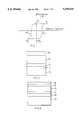
- FIG. 2shows a schematic of a ferroelectric capacitor in which the ferroelectric material is layered structure oxide.
- the ferroelectric capacitoris built on top of a substrate material 10 that may be silicon, a layer of silicon dioxide over a silicon chip, gallium arsenide, MgO, sapphire etc.
- the substrate 10may be a multilayer structure having various circuit elements formed on a silicon chip having layers of silicon dioxide, polysilicon, implanted silicon layers etc. to form a complex integrated circuit.
- a thin bottom electrode layer 12is deposited on top of the substrate by any of the standard PVD processes or chemical processes of thin film deposition mentioned earlier.
- an intermediate adhesion layer (11)may be included to improve the adhesion between the bottom electrode and the substrate material.
- a thin Ti interlayeris added to improve the adhesion between Pt and SiO 2 .
- the ferroelectric material 13which is a layered structure oxide, is then deposited on the bottom electrode by the processes of the invention described later.
- the top electrode materialis then either deposited through a shadow mask to form the electrodes of the required area directly or deposited completely over the ferroelectric films and later etched after suitable masking using one of the standard VLSI etching processes such as reactive ion etching, wet etching, ion milling, plasma etching etc. to make several capacitors on a wafer.
- the materials of the top electrodemay either be the same as used for the bottom electrodes or any combination thereof.
- buffer layers 15 and 16may be added between the ferroelectric layer 13 and the electrodes 12 and 14 at the bottom and top, respectively, as shown in FIG. 3.
- the selection of the precursorsis the most critical step in MOCVD for successful deposition of complex oxide films.
- the ideal precursors for MOCVDhave to meet the requirements of high vapor pressure at low vaporization temperatures, low decomposition temperatures, large "window” between vaporization and decomposition temperatures, no contamination form organic constituents of the precursors, stability under ambient conditions and nontoxicity.
- several types of metallorganic compoundshave been used as precursors to grow the complex layered structure films. These include metal alkyls, metal alkoxides, metal ⁇ -didetonates and metallocenes. Most of the metaloxide precursors have reasonable vapor pressures at relatively low temperatures.
- metal oxides and metal ⁇ -diketonatesare less volatile than their alkyl equivalents, but they are easier to handle and much less toxic.
- One of the assets of metallorganic precursorsis that their physical and chemical properties can be tailored by making small changes in their chemical structure. For example, the volatility of a metal ⁇ -diketonate can be increased by varying the alkyl or fluoroalkyl group on the chelating ring.
- FIG. 4A schematic of the hot wall MOCVD apparatus 40 used in the present invention is shown in FIG. 4.
- the reaction chamber 50was a stainless steel tube having an inside diameter of 75 mm.
- the chamber 50was pumped to low pressures before deposition by a mechanical pump 52 and the pressure inside the chamber 50 was monitored by an MKS BARATRON pressure sensor 54. This sensor could monitor pressures in the range of 12 to 10 -3 Torr.
- the temperature inside the chamber 50was maintained by a resistively heated three zone furnace 58.
- a cold trap 60was placed between the reaction chamber 50 and the mechanical pump 52.
- the precursor materialwas packaged in a stainless steel bubbler 62 with two connections; one was connected to the reactor by a stainless steel line 64 with a manual valve 66 and the other was connected to a N 2 gas cylinder 70 with a mass flow controller 72.
- Aluminum housed mantle heaters with temperature controllerswere used to control the temperatures of the precursors.
- the precursorswere kept at the desired temperatures within ⁇ 5° C. during deposition.
- the paths between the furnace and the precursor bubblerswere heated by heating tapes to a temperature ranging from 200° to 300° C. to prevent condensation or decomposition of the precursors.
- the apparatus of FIG. 4shows several bubblers with their associated lines, mass flow controllers and gas cylinders.
- FIG. 5A schematic of the cold-wall MOCVD apparatus 80 used in the present invention is shown in FIG. 5.
- a three inch diameter substrate heater 82that could be operated at a maximum temperature of 900 ° C. was employed.
- the temperature of the substrate heater 82was position insensitive within an 8° C. range, and the variation in the temperature with time throughout the growth process was within 1° C.
- a substrate holder 84made of INCONEL and placed in direct contact with the substrate heater 82, was used to hold the substrates 86.
- the substrate temperaturewas monitored by a thermocouple 88 which was placed inside the center of the substrate holder 84.
- the specimenswere adhered on the substrate holder by silver paste.
- the silver pastewas used to improve the heat conduction and temperature uniformity of specimens.
- the distance between the inlet 90 of the source mixture and the substrates 86could be varied form 1.5 to 10 cm.
- the setup and control of the bypass line and the bubbler heaterswere similar to those of the hot-wall apparatus.
- the bubblers used in the present inventionhave a cylindrical shape 1.5 inches in diameter and 6 inches high.
- the precursor materialsare solids which decompose at temperatures close to the temperature at which they sublime.
- the bubbleris held at sufficiently high temperatures to sublime the reagents and consequently significant decomposition of the growth reagents may occur during deposition leading to variations in the composition and poor reproducibility between different runs.
- volatile source reagentswe have also incorporated a method of liquid source delivery.
- the reagent sourceis held in the form of a liquid (for solid sources, a solvent is added to make it in the form of a liquid) and vaporized on a vaporization matrix structure at an elevated temperature.
- the vapor sourceis then transferred into the pyrolysis chamber of the MOCVD reactor by a carrier gas that flows past the vaporization matrix.
- a schematic of the liquid source delivery system used as a part of the present inventionis shown in FIG. 6.
- the source materials of the desired thin film compoundwere mixed stoichiometrically and held in the liquid form in an Erlenmeyer flask 110.
- the sourcewas transferred to the flash vaporization chamber 102 by a Masterflex Economy drive 128 (basically a pump with liquid flow meter) through a series of tubes as shown in FIG. 6.
- a needle valve 104was inserted in the flow line to control the flow of the liquid and was connected to the source end by silicone tubing 106 and the vaporization chamber end by stainless steel tubing 108.
- the sourcewas transferred from the flask 110 to the silicone tubing 106 through a glass rod.
- the vaporization chamber 102was sealed on the source end by a flange 114.
- the stainless steel tube 108 that provides the path for the liquid source deliverywas inserted into the vaporization chamber 102 through a tight fit hole drilled into the flange 114.
- the other end of the chamber 102was connected to the pyrolysis chamber of the MOCVD reactor, the temperature of which is controlled by a preheat chamber temperature controller 132.
- the vaporization chamber 102was heated as a whole and the temperature was controlled using a temperature controller 118.
- a preheated carrier gas (N 2 )was used to transport the vaporized source from the vaporization chamber 102 to the pyrolysis chamber.
- the flow rate of the carrier gaswas controlled using a mass flow controller 130.
- the carrier gaswas sent through a preheat chamber 120 to heat the gases.
- This whole systemis termed as direct liquid injection (DLI) and the MOCVD process performed using this method of source vaporization is known as DLI-MOCVD. See U.S. Pat. No. 5,204,314 by Kirlin.
- the substratesare loaded, the reaction chamber is sealed, and the system is evacuated to a desired pressure.
- the reaction chamber and/or substratehot wall and cold wall
- the bubbler(FIGS. 4 and 5) configuration is used for vaporization of the source materials, then the source bubblers are directly heated to the desired temperatures.
- the source liquid(stoichiometric mix of the individual precursors for each element in the final compound) is transferred to the vaporization chamber and vaporized at a temperature of around 250° C. on the evaporation matrix and carried to the deposition chamber by a carrier N 2 gas also preheated to the same temperature.
- the source vapors accompanied by nitrogen carrier gasare sent through the bypass line; oxygen is sent through the reaction chamber to minimize the back diffusion of source vapors into the chamber.
- the bypass processis performed for about 3 minutes before beginning the deposition process.
- the bypass valveis closed and the main valve of the reaction chamber is opened to start the deposition.
- the flow of the vapors from the bubblers or the DLI systemis maintained for a predetermined deposition time.
- the vaporization chamber and carrier gasare shut off, and the reactor is evacuated to base pressure before backfilling with air to atmospheric pressure.
- the samplesare furnace-cooled below 100° C. before they were removed from the reactor.
- the precursors for depositing the layered structure oxidescan be one of metal alkyls, metal alkoxides, metal ⁇ -diketonates, and metallocenes.
- the preferred precursors for depositing SrBi 2 (Ta x Nb 2-x )O 9 or BaBi 2 (Ta x Nb 2-x )O 9are
- BaBa(thd) 2 (Ba-tetramethylheptadione),
- BiBi(thd) 3 (Bi-tetramethylheptadione),
- TaTa(OC 2 H 5 ) 5 (Ta-ethoxide),
- NbNb(OC 2 H 5 ) 5 (Nb-ethoxide).
- these precursorsare mixed in stoichiometric ratios in a solvent that is a 8:2:1 mixture in moles of tetrahydrofuran (C 4 H 8 O), iso-propanol (C 4 H 10 O), and tetraglyme (C 10 H 22 O 5 ). If the conventional bubbler method is used, the individual precursors are packed into bubblers which are then heated to vaporize the precursors.
- FIGS. 7-9The superior ferroelectric properties of the layered structure oxides can be illustrated by FIGS. 7-9.
- the ferroelectric films shown in these figuresare SrBi 2 (Ta 0 .8 Nb 1 .2)O 9 deposited by pulsed laser deposition (PLD) method. The bottom and top electrodes were sputtered Pt.
- FIG. 7shows the hysteresis characteristics of PLD SrBi 2 (Ta 0 .8 Nb 1 .2)O 9 films at an applied voltage of 5 V. The hysteresis loop is well saturated at this voltage and shows a Pr value of 11 ⁇ C/cm 2 and an Ec value of 65 KV/cm.
- FIG. 8shows the result of the fatigue test performed up to 10 9 cycles.
- the filmsshow very low fatigue rate.
- the hysteresis properties on the films measured after cyclingare shown in FIG. 9.
- the hysteresis properties of the films before and after cyclingwere similar.
- the leakage current density values for these filmswere measured as a function of applied voltage. At an applied voltage of 3 V, the films showed a leakage current density of 10 -7 A/cm 2 .
- the measured resistivity of filmswere typically of the order of 10 -12 ohm-cm.
- the process of inventioncan be used to fabricate high quality layered structure oxide thin films for ferroelectric nonvolatile random access memory applications.
- the processcan also be applied to fabricate these materials for other applications such as piezoelectric, pyroelectric, electro-optic etc.
- the processmay be applied to deposit these materials onto structures (may be with different dimensions) other than that described specifically (capacitors) in the present invention.
- the processmay also be modified to add further processing steps.
- the basic inventive concept of the inventionis still the same.
Landscapes
- Engineering & Computer Science (AREA)
- Chemical & Material Sciences (AREA)
- Physics & Mathematics (AREA)
- Chemical Kinetics & Catalysis (AREA)
- Manufacturing & Machinery (AREA)
- Microelectronics & Electronic Packaging (AREA)
- Power Engineering (AREA)
- General Physics & Mathematics (AREA)
- Condensed Matter Physics & Semiconductors (AREA)
- Computer Hardware Design (AREA)
- General Chemical & Material Sciences (AREA)
- Plasma & Fusion (AREA)
- Inorganic Chemistry (AREA)
- Materials Engineering (AREA)
- Mechanical Engineering (AREA)
- Metallurgy (AREA)
- Organic Chemistry (AREA)
- Chemical Vapour Deposition (AREA)
- Semiconductor Memories (AREA)
Abstract
Description
A.sub.A +B.sub.B +3O.sub.o →V.sub.A "+V.sub.B ""+3V.sub.o.sup.oo +A.sub.s +B.sub.s +3O.sub.s ( 1)
Pb.sub.Pb +Ti.sub.Ti +Zr.sub.Zr +3O.sub.o →xPbO+xV.sub.Pb "+xV.sub.o.sup.oo +(1-x)Pb.sub.Pb +Ti.sub.Ti +Zr.sub.Zr +(1-x) O.sub.o( 2)
Claims (26)
Priority Applications (5)
| Application Number | Priority Date | Filing Date | Title |
|---|---|---|---|
| US08/300,339US5478610A (en) | 1994-09-02 | 1994-09-02 | Metalorganic chemical vapor deposition of layered structure oxides |
| US08/393,233US5873977A (en) | 1994-09-02 | 1995-02-22 | Dry etching of layer structure oxides |
| US08/454,029US5527567A (en) | 1994-09-02 | 1995-05-30 | Metalorganic chemical vapor deposition of layered structure oxides |
| JP07190899AJP3114916B2 (en) | 1994-09-02 | 1995-07-26 | Dry etching method of layered structure oxide thin film |
| JP21077495AJP3436617B2 (en) | 1994-09-02 | 1995-08-18 | Manufacturing method of ferroelectric thin film |
Applications Claiming Priority (1)
| Application Number | Priority Date | Filing Date | Title |
|---|---|---|---|
| US08/300,339US5478610A (en) | 1994-09-02 | 1994-09-02 | Metalorganic chemical vapor deposition of layered structure oxides |
Related Child Applications (2)
| Application Number | Title | Priority Date | Filing Date |
|---|---|---|---|
| US08/393,233Continuation-In-PartUS5873977A (en) | 1994-09-02 | 1995-02-22 | Dry etching of layer structure oxides |
| US08/454,029Continuation-In-PartUS5527567A (en) | 1994-09-02 | 1995-05-30 | Metalorganic chemical vapor deposition of layered structure oxides |
Publications (1)
| Publication Number | Publication Date |
|---|---|
| US5478610Atrue US5478610A (en) | 1995-12-26 |
Family
ID=23158694
Family Applications (1)
| Application Number | Title | Priority Date | Filing Date |
|---|---|---|---|
| US08/300,339Expired - LifetimeUS5478610A (en) | 1994-09-02 | 1994-09-02 | Metalorganic chemical vapor deposition of layered structure oxides |
Country Status (1)
| Country | Link |
|---|---|
| US (1) | US5478610A (en) |
Cited By (75)
| Publication number | Priority date | Publication date | Assignee | Title |
|---|---|---|---|---|
| US5605723A (en)* | 1994-05-16 | 1997-02-25 | Mitsubishi Materials Corporation | Method for forming a pattern of non-volatile ferroelectric thin film memory |
| US5648114A (en)* | 1991-12-13 | 1997-07-15 | Symetrix Corporation | Chemical vapor deposition process for fabricating layered superlattice materials |
| US5674563A (en)* | 1993-09-14 | 1997-10-07 | Nissan Motor Co., Ltd. | Method for ferroelectric thin film production |
| EP0807965A3 (en)* | 1996-05-14 | 1998-02-04 | Matsushita Electronics Corporation | Method of manufacturing layered ferroelectric Bi containing film |
| US5784310A (en)* | 1997-03-03 | 1998-07-21 | Symetrix Corporation | Low imprint ferroelectric material for long retention memory and method of making the same |
| US5803961A (en)* | 1992-10-23 | 1998-09-08 | Symetrix Corporation | Integrated circuits having mixed layered superlattice materials and precursor solutions for use in a process of making the same |
| US5804823A (en)* | 1995-10-10 | 1998-09-08 | Raytheon Company | Bismuth layered structure pyroelectric detectors |
| US5820946A (en)* | 1995-05-10 | 1998-10-13 | Korea Institute Of Science And Technology | Method for fabricating ferroelectric thin film |
| WO1999000530A1 (en)* | 1997-06-26 | 1999-01-07 | Advanced Technology Materials, Inc. | Low temperature chemical vapor deposition process for forming bismuth-containing ceramic thin films useful in ferroelectric memory devices |
| DE19730119A1 (en)* | 1997-07-14 | 1999-01-21 | Siemens Ag | Process for the production of thin films from oxidic ceramics |
| US5897912A (en)* | 1997-09-03 | 1999-04-27 | Ferro Corporation | Method of making conductive electrodes for use in multilayer ceramic capacitors or inductors using organometallic ink |
| DE19806013A1 (en)* | 1998-02-16 | 1999-09-23 | Forschungszentrum Juelich Gmbh | Crystallization of ceramic layers especially electronic ceramic thin films for integration with microelectronic and micromechanical devices e.g. for Fe-RAM production |
| US6072207A (en)* | 1991-02-25 | 2000-06-06 | Symetrix Corporation | Process for fabricating layered superlattice materials and making electronic devices including same |
| US6111122A (en)* | 1998-04-28 | 2000-08-29 | Advanced Technology Materials, Inc. | Group II MOCVD source reagents, and method of forming Group II metal-containing films utilizing same |
| US6110531A (en)* | 1991-02-25 | 2000-08-29 | Symetrix Corporation | Method and apparatus for preparing integrated circuit thin films by chemical vapor deposition |
| US6120846A (en)* | 1997-12-23 | 2000-09-19 | Advanced Technology Materials, Inc. | Method for the selective deposition of bismuth based ferroelectric thin films by chemical vapor deposition |
| US6127218A (en)* | 1996-05-25 | 2000-10-03 | Samsung Electronics Co., Ltd. | Methods for forming ferroelectric films using dual deposition steps |
| US6133051A (en)* | 1998-06-30 | 2000-10-17 | Advanced Technology Materials, Inc. | Amorphously deposited metal oxide ceramic films |
| US6159855A (en)* | 1998-04-28 | 2000-12-12 | Micron Technology, Inc. | Organometallic compound mixtures in chemical vapor deposition |
| US6177135B1 (en) | 1997-03-31 | 2001-01-23 | Advanced Technology Materials, Inc. | Low temperature CVD processes for preparing ferroelectric films using Bi amides |
| US6180420B1 (en) | 1997-12-10 | 2001-01-30 | Advanced Technology Materials, Inc. | Low temperature CVD processes for preparing ferroelectric films using Bi carboxylates |
| WO2001036705A1 (en)* | 1999-11-15 | 2001-05-25 | Advanced Technology Materials, Inc. | Liquid delivery mocvd of sbt |
| US6251360B1 (en)* | 1995-03-30 | 2001-06-26 | Sony Corporation | Method of producing bismuth layered compound |
| CN1068729C (en)* | 1996-01-22 | 2001-07-18 | 伊利诺斯工具工程有限公司 | Axial pole motor |
| US6312816B1 (en)* | 1998-02-20 | 2001-11-06 | Advanced Technology Materials, Inc. | A-site- and/or B-site-modified PbZrTiO3 materials and (Pb, Sr, Ca, Ba, Mg) (Zr, Ti, Nb, Ta)O3 films having utility in ferroelectric random access memories and high performance thin film microactuators |
| US6340386B1 (en)* | 1998-12-31 | 2002-01-22 | Advanced Technology Materials, Inc. | MOCVD of SBT using toluene based solvent system for precursor delivery |
| US6428623B2 (en)* | 1993-05-14 | 2002-08-06 | Micron Technology, Inc. | Chemical vapor deposition apparatus with liquid feed |
| US20020166507A1 (en)* | 1999-03-12 | 2002-11-14 | Tokyo Electron Limited | Thin film forming apparatus |
| US6500489B1 (en) | 1996-11-27 | 2002-12-31 | Advanced Technology Materials, Inc. | Low temperature CVD processes for preparing ferroelectric films using Bi alcoxides |
| US20030000058A1 (en)* | 2001-06-27 | 2003-01-02 | Asia Pacific Microsystems, Inc. | Method for manufacturing a film bulk acoustic wave filter |
| US6511706B1 (en)* | 1990-07-06 | 2003-01-28 | Advanced Technology Materials, Inc. | MOCVD of SBT using tetrahydrofuran-based solvent system for precursor delivery |
| US6541375B1 (en)* | 1998-06-30 | 2003-04-01 | Matsushita Electric Industrial Co., Ltd. | DC sputtering process for making smooth electrodes and thin film ferroelectric capacitors having improved memory retention |
| US20030103372A1 (en)* | 2001-11-30 | 2003-06-05 | Sanyo Electric Co., Ltd. | Ferroelectric memory and operating method therefor |
| US6664115B2 (en)* | 1992-10-23 | 2003-12-16 | Symetrix Corporation | Metal insulator structure with polarization-compatible buffer layer |
| US6756235B1 (en) | 1999-08-20 | 2004-06-29 | Tokyo Electron Limited | Metal oxide film formation method and apparatus |
| US6787186B1 (en) | 1997-12-18 | 2004-09-07 | Advanced Technology Materials, Inc. | Method of controlled chemical vapor deposition of a metal oxide ceramic layer |
| US20040209384A1 (en)* | 1997-11-20 | 2004-10-21 | Hintermaier Frank S | Low temperature chemical vapor deposition process for forming bismuth-containing ceramic thin films useful in ferroelectric memory devices |
| US20040219746A1 (en)* | 2003-04-29 | 2004-11-04 | Micron Technology, Inc. | Systems and methods for forming metal oxide layers |
| US6974985B2 (en)* | 2001-01-31 | 2005-12-13 | Fujitsu Limited | Capacitor and method for fabricating the same, and semiconductor device and method for fabricating the same |
| US20060021573A1 (en)* | 2004-06-28 | 2006-02-02 | Cambridge Nanotech Inc. | Vapor deposition systems and methods |
| KR100648142B1 (en)* | 1999-07-07 | 2006-11-24 | 소니 가부시끼 가이샤 | A method for fabricating dielectric films |
| US20070006798A1 (en)* | 2002-08-28 | 2007-01-11 | Micron Technology, Inc. | Systems and methods for forming strontium-and/or barium-containing layers |
| US7332032B2 (en) | 1999-06-16 | 2008-02-19 | Micron Technology, Inc. | Precursor mixtures for use in preparing layers on substrates |
| US20080121181A1 (en)* | 2000-03-31 | 2008-05-29 | Tanaka Kikinzoku Kogyo K.K. | Cvd process for forming a thin film |
| US20090107586A1 (en)* | 2007-10-31 | 2009-04-30 | Kabushiki Kaisha Toshiba | Method for manufacturing a lanthanum oxide compound |
| WO2012018581A3 (en)* | 2010-07-26 | 2012-03-22 | De Rochemont L Pierre | Liquid chemical deposition apparatus and process and products therefrom |
| US8552708B2 (en) | 2010-06-02 | 2013-10-08 | L. Pierre de Rochemont | Monolithic DC/DC power management module with surface FET |
| US8593819B2 (en) | 2004-10-01 | 2013-11-26 | L. Pierre de Rochemont | Ceramic antenna module and methods of manufacture thereof |
| US8749054B2 (en) | 2010-06-24 | 2014-06-10 | L. Pierre de Rochemont | Semiconductor carrier with vertical power FET module |
| US8922347B1 (en) | 2009-06-17 | 2014-12-30 | L. Pierre de Rochemont | R.F. energy collection circuit for wireless devices |
| US8952858B2 (en) | 2009-06-17 | 2015-02-10 | L. Pierre de Rochemont | Frequency-selective dipole antennas |
| US9023493B2 (en) | 2010-07-13 | 2015-05-05 | L. Pierre de Rochemont | Chemically complex ablative max-phase material and method of manufacture |
| US9123768B2 (en) | 2010-11-03 | 2015-09-01 | L. Pierre de Rochemont | Semiconductor chip carriers with monolithically integrated quantum dot devices and method of manufacture thereof |
| US9905928B2 (en) | 2005-06-30 | 2018-02-27 | L. Pierre de Rochemont | Electrical components and method of manufacture |
| US10468256B2 (en)* | 2015-08-04 | 2019-11-05 | Samsung Electronics Co., Ltd. | Methods of forming material layer |
| US20200091308A1 (en)* | 2018-09-13 | 2020-03-19 | Intel Corporation | Improper ferroelectric active and passive devices |
| US10943733B2 (en) | 2018-03-09 | 2021-03-09 | Samsung Electronics Co., Ltd. | Ceramic dielectric and method of manufacturing the same and ceramic electronic component and electronic device |
| USD940149S1 (en) | 2017-06-08 | 2022-01-04 | Insulet Corporation | Display screen with a graphical user interface |
| USD977502S1 (en) | 2020-06-09 | 2023-02-07 | Insulet Corporation | Display screen with graphical user interface |
| US11857763B2 (en) | 2016-01-14 | 2024-01-02 | Insulet Corporation | Adjusting insulin delivery rates |
| US11865299B2 (en) | 2008-08-20 | 2024-01-09 | Insulet Corporation | Infusion pump systems and methods |
| US11929158B2 (en) | 2016-01-13 | 2024-03-12 | Insulet Corporation | User interface for diabetes management system |
| USD1020794S1 (en) | 2018-04-02 | 2024-04-02 | Bigfoot Biomedical, Inc. | Medication delivery device with icons |
| USD1024090S1 (en) | 2019-01-09 | 2024-04-23 | Bigfoot Biomedical, Inc. | Display screen or portion thereof with graphical user interface associated with insulin delivery |
| US11969579B2 (en) | 2017-01-13 | 2024-04-30 | Insulet Corporation | Insulin delivery methods, systems and devices |
| US11976355B2 (en)* | 2020-09-29 | 2024-05-07 | Centre National De La Recherche Scientifique | Method for manufacturing an environmental barrier |
| US12042630B2 (en) | 2017-01-13 | 2024-07-23 | Insulet Corporation | System and method for adjusting insulin delivery |
| US12064591B2 (en) | 2013-07-19 | 2024-08-20 | Insulet Corporation | Infusion pump system and method |
| US12076160B2 (en) | 2016-12-12 | 2024-09-03 | Insulet Corporation | Alarms and alerts for medication delivery devices and systems |
| US12097355B2 (en) | 2023-01-06 | 2024-09-24 | Insulet Corporation | Automatically or manually initiated meal bolus delivery with subsequent automatic safety constraint relaxation |
| US12106837B2 (en) | 2016-01-14 | 2024-10-01 | Insulet Corporation | Occlusion resolution in medication delivery devices, systems, and methods |
| US12318577B2 (en) | 2017-01-13 | 2025-06-03 | Insulet Corporation | System and method for adjusting insulin delivery |
| US12318594B2 (en) | 2016-05-26 | 2025-06-03 | Insulet Corporation | On-body interlock for drug delivery device |
| US12343502B2 (en) | 2017-01-13 | 2025-07-01 | Insulet Corporation | System and method for adjusting insulin delivery |
| US12383166B2 (en) | 2016-05-23 | 2025-08-12 | Insulet Corporation | Insulin delivery system and methods with risk-based set points |
- 1994
- 1994-09-02USUS08/300,339patent/US5478610A/ennot_activeExpired - Lifetime
Cited By (124)
| Publication number | Priority date | Publication date | Assignee | Title |
|---|---|---|---|---|
| US6511706B1 (en)* | 1990-07-06 | 2003-01-28 | Advanced Technology Materials, Inc. | MOCVD of SBT using tetrahydrofuran-based solvent system for precursor delivery |
| US6072207A (en)* | 1991-02-25 | 2000-06-06 | Symetrix Corporation | Process for fabricating layered superlattice materials and making electronic devices including same |
| US6110531A (en)* | 1991-02-25 | 2000-08-29 | Symetrix Corporation | Method and apparatus for preparing integrated circuit thin films by chemical vapor deposition |
| US5648114A (en)* | 1991-12-13 | 1997-07-15 | Symetrix Corporation | Chemical vapor deposition process for fabricating layered superlattice materials |
| US5840110A (en)* | 1992-10-23 | 1998-11-24 | Symetrix Corporation | Integrated circuits having mixed layered superlattice materials and precursor solutions for use in a process of making the same |
| US6664115B2 (en)* | 1992-10-23 | 2003-12-16 | Symetrix Corporation | Metal insulator structure with polarization-compatible buffer layer |
| US5803961A (en)* | 1992-10-23 | 1998-09-08 | Symetrix Corporation | Integrated circuits having mixed layered superlattice materials and precursor solutions for use in a process of making the same |
| US5955754A (en)* | 1992-10-23 | 1999-09-21 | Symetrix Corporation | Integrated circuits having mixed layered superlattice materials and precursor solutions for use in a process of making the same |
| US6428623B2 (en)* | 1993-05-14 | 2002-08-06 | Micron Technology, Inc. | Chemical vapor deposition apparatus with liquid feed |
| US7182979B2 (en) | 1993-05-14 | 2007-02-27 | Micron Technology, Inc. | High efficiency method for performing a chemical vapordeposition utilizing a nonvolatile precursor |
| US20020192376A1 (en)* | 1993-05-14 | 2002-12-19 | Micron Technology, Inc. | High efficiency method for performing a chemical vapordeposition utilizing a nonvolatile precursor |
| US5674563A (en)* | 1993-09-14 | 1997-10-07 | Nissan Motor Co., Ltd. | Method for ferroelectric thin film production |
| US5605723A (en)* | 1994-05-16 | 1997-02-25 | Mitsubishi Materials Corporation | Method for forming a pattern of non-volatile ferroelectric thin film memory |
| US6251360B1 (en)* | 1995-03-30 | 2001-06-26 | Sony Corporation | Method of producing bismuth layered compound |
| US5820946A (en)* | 1995-05-10 | 1998-10-13 | Korea Institute Of Science And Technology | Method for fabricating ferroelectric thin film |
| US5804823A (en)* | 1995-10-10 | 1998-09-08 | Raytheon Company | Bismuth layered structure pyroelectric detectors |
| CN1068729C (en)* | 1996-01-22 | 2001-07-18 | 伊利诺斯工具工程有限公司 | Axial pole motor |
| EP0807965A3 (en)* | 1996-05-14 | 1998-02-04 | Matsushita Electronics Corporation | Method of manufacturing layered ferroelectric Bi containing film |
| US6127218A (en)* | 1996-05-25 | 2000-10-03 | Samsung Electronics Co., Ltd. | Methods for forming ferroelectric films using dual deposition steps |
| US6500489B1 (en) | 1996-11-27 | 2002-12-31 | Advanced Technology Materials, Inc. | Low temperature CVD processes for preparing ferroelectric films using Bi alcoxides |
| US5784310A (en)* | 1997-03-03 | 1998-07-21 | Symetrix Corporation | Low imprint ferroelectric material for long retention memory and method of making the same |
| US6177135B1 (en) | 1997-03-31 | 2001-01-23 | Advanced Technology Materials, Inc. | Low temperature CVD processes for preparing ferroelectric films using Bi amides |
| US6730523B2 (en) | 1997-06-26 | 2004-05-04 | Advanced Technology Materials, Inc. | Low temperature chemical vapor deposition process for forming bismuth-containing ceramic thin films useful in ferroelectric memory devices |
| WO1999000530A1 (en)* | 1997-06-26 | 1999-01-07 | Advanced Technology Materials, Inc. | Low temperature chemical vapor deposition process for forming bismuth-containing ceramic thin films useful in ferroelectric memory devices |
| US6303391B1 (en) | 1997-06-26 | 2001-10-16 | Advanced Technology Materials, Inc. | Low temperature chemical vapor deposition process for forming bismuth-containing ceramic films useful in ferroelectric memory devices |
| US6037002A (en)* | 1997-07-14 | 2000-03-14 | Siemens Aktiengesellschaft | Process for producing thin films of oxide ceramic |
| DE19730119A1 (en)* | 1997-07-14 | 1999-01-21 | Siemens Ag | Process for the production of thin films from oxidic ceramics |
| US5897912A (en)* | 1997-09-03 | 1999-04-27 | Ferro Corporation | Method of making conductive electrodes for use in multilayer ceramic capacitors or inductors using organometallic ink |
| US20040209384A1 (en)* | 1997-11-20 | 2004-10-21 | Hintermaier Frank S | Low temperature chemical vapor deposition process for forming bismuth-containing ceramic thin films useful in ferroelectric memory devices |
| US7005303B2 (en) | 1997-11-20 | 2006-02-28 | Advanced Technology Materials, Inc. | Low temperature chemical vapor deposition process for forming bismuth-containing ceramic thin films useful in ferroelectric memory devices |
| US6180420B1 (en) | 1997-12-10 | 2001-01-30 | Advanced Technology Materials, Inc. | Low temperature CVD processes for preparing ferroelectric films using Bi carboxylates |
| US6787186B1 (en) | 1997-12-18 | 2004-09-07 | Advanced Technology Materials, Inc. | Method of controlled chemical vapor deposition of a metal oxide ceramic layer |
| US6120846A (en)* | 1997-12-23 | 2000-09-19 | Advanced Technology Materials, Inc. | Method for the selective deposition of bismuth based ferroelectric thin films by chemical vapor deposition |
| DE19806013A1 (en)* | 1998-02-16 | 1999-09-23 | Forschungszentrum Juelich Gmbh | Crystallization of ceramic layers especially electronic ceramic thin films for integration with microelectronic and micromechanical devices e.g. for Fe-RAM production |
| DE19806013C2 (en)* | 1998-02-16 | 2003-10-30 | Forschungszentrum Juelich Gmbh | Process for producing a crystallized ceramic thin film |
| US6312816B1 (en)* | 1998-02-20 | 2001-11-06 | Advanced Technology Materials, Inc. | A-site- and/or B-site-modified PbZrTiO3 materials and (Pb, Sr, Ca, Ba, Mg) (Zr, Ti, Nb, Ta)O3 films having utility in ferroelectric random access memories and high performance thin film microactuators |
| US6350686B1 (en) | 1998-04-28 | 2002-02-26 | Micron Technology, Inc. | Organometallic compound mixtures in chemical vapor deposition |
| US6338873B1 (en) | 1998-04-28 | 2002-01-15 | Advanced Technology Materials, Inc. | Method of forming Group II metal-containing films utilizing Group II MOCVD source reagents |
| US6111122A (en)* | 1998-04-28 | 2000-08-29 | Advanced Technology Materials, Inc. | Group II MOCVD source reagents, and method of forming Group II metal-containing films utilizing same |
| US6624072B2 (en) | 1998-04-28 | 2003-09-23 | Micron Technology, Inc. | Organometallic compound mixtures in chemical vapor deposition |
| US6159855A (en)* | 1998-04-28 | 2000-12-12 | Micron Technology, Inc. | Organometallic compound mixtures in chemical vapor deposition |
| US6348412B1 (en) | 1998-04-28 | 2002-02-19 | Micron Technology, Inc. | Organometallic compound mixtures in chemical vapor deposition |
| US6541375B1 (en)* | 1998-06-30 | 2003-04-01 | Matsushita Electric Industrial Co., Ltd. | DC sputtering process for making smooth electrodes and thin film ferroelectric capacitors having improved memory retention |
| US6133051A (en)* | 1998-06-30 | 2000-10-17 | Advanced Technology Materials, Inc. | Amorphously deposited metal oxide ceramic films |
| US6660331B2 (en) | 1998-12-31 | 2003-12-09 | Advanced Technology Materials, Inc. | MOCVD of SBT using toluene-based solvent system for precursor delivery |
| US6340386B1 (en)* | 1998-12-31 | 2002-01-22 | Advanced Technology Materials, Inc. | MOCVD of SBT using toluene based solvent system for precursor delivery |
| US20020166507A1 (en)* | 1999-03-12 | 2002-11-14 | Tokyo Electron Limited | Thin film forming apparatus |
| US6866882B1 (en) | 1999-03-12 | 2005-03-15 | Tokyo Electron Limited | Method of forming a thin film |
| US7332032B2 (en) | 1999-06-16 | 2008-02-19 | Micron Technology, Inc. | Precursor mixtures for use in preparing layers on substrates |
| KR100648142B1 (en)* | 1999-07-07 | 2006-11-24 | 소니 가부시끼 가이샤 | A method for fabricating dielectric films |
| US6756235B1 (en) | 1999-08-20 | 2004-06-29 | Tokyo Electron Limited | Metal oxide film formation method and apparatus |
| WO2001036705A1 (en)* | 1999-11-15 | 2001-05-25 | Advanced Technology Materials, Inc. | Liquid delivery mocvd of sbt |
| US20080121181A1 (en)* | 2000-03-31 | 2008-05-29 | Tanaka Kikinzoku Kogyo K.K. | Cvd process for forming a thin film |
| US6974985B2 (en)* | 2001-01-31 | 2005-12-13 | Fujitsu Limited | Capacitor and method for fabricating the same, and semiconductor device and method for fabricating the same |
| US20030000058A1 (en)* | 2001-06-27 | 2003-01-02 | Asia Pacific Microsystems, Inc. | Method for manufacturing a film bulk acoustic wave filter |
| US7167386B2 (en)* | 2001-11-30 | 2007-01-23 | Sanyo Electric Co., Ltd. | Ferroelectric memory and operating method therefor |
| US20030103372A1 (en)* | 2001-11-30 | 2003-06-05 | Sanyo Electric Co., Ltd. | Ferroelectric memory and operating method therefor |
| US9735148B2 (en) | 2002-02-19 | 2017-08-15 | L. Pierre de Rochemont | Semiconductor carrier with vertical power FET module |
| US20070006798A1 (en)* | 2002-08-28 | 2007-01-11 | Micron Technology, Inc. | Systems and methods for forming strontium-and/or barium-containing layers |
| US20080210157A9 (en)* | 2002-08-28 | 2008-09-04 | Micron Technology, Inc. | Systems and methods for forming strontium-and/or barium-containing layers |
| US8617312B2 (en) | 2002-08-28 | 2013-12-31 | Micron Technology, Inc. | Systems and methods for forming layers that contain niobium and/or tantalum |
| US7482284B2 (en) | 2003-04-29 | 2009-01-27 | Micron Technology, Inc. | Deposition methods for forming silicon oxide layers |
| US7332442B2 (en) | 2003-04-29 | 2008-02-19 | Micron Technology, Inc. | Systems and methods for forming metal oxide layers |
| US20060252244A1 (en)* | 2003-04-29 | 2006-11-09 | Micron Technology, Inc. | Systems and methods for forming metal oxide layers |
| US8394725B2 (en) | 2003-04-29 | 2013-03-12 | Micron Technology, Inc. | Systems and methods for forming metal oxide layers |
| US20040219746A1 (en)* | 2003-04-29 | 2004-11-04 | Micron Technology, Inc. | Systems and methods for forming metal oxide layers |
| US7115528B2 (en) | 2003-04-29 | 2006-10-03 | Micron Technology, Inc. | Systems and method for forming silicon oxide layers |
| US20090149033A1 (en)* | 2003-04-29 | 2009-06-11 | Micron Technology, Inc. | Systems and methods for forming metal oxide layers |
| US7678708B2 (en) | 2003-04-29 | 2010-03-16 | Micron Technology, Inc. | Systems and methods for forming metal oxide layers |
| US20070155190A1 (en)* | 2003-04-29 | 2007-07-05 | Micron Technology, Inc. | Systems and methods for forming metal oxide layers |
| US20100147218A1 (en)* | 2003-04-29 | 2010-06-17 | Micron Technology, Inc. | Systems and methods for forming metal oxide layers |
| US8114219B2 (en) | 2003-04-29 | 2012-02-14 | Micron Technology, Inc. | Systems and methods for forming metal oxide layers |
| US9556519B2 (en)* | 2004-06-28 | 2017-01-31 | Ultratech Inc. | Vapor deposition systems and methods |
| US8202575B2 (en)* | 2004-06-28 | 2012-06-19 | Cambridge Nanotech, Inc. | Vapor deposition systems and methods |
| US20120070581A1 (en)* | 2004-06-28 | 2012-03-22 | Cambridge Nano Tech Inc. | Vapor deposition systems and methods |
| US20060021573A1 (en)* | 2004-06-28 | 2006-02-02 | Cambridge Nanotech Inc. | Vapor deposition systems and methods |
| US9520649B2 (en) | 2004-10-01 | 2016-12-13 | L. Pierre de Rochemont | Ceramic antenna module and methods of manufacture thereof |
| US8593819B2 (en) | 2004-10-01 | 2013-11-26 | L. Pierre de Rochemont | Ceramic antenna module and methods of manufacture thereof |
| US9882274B2 (en) | 2004-10-01 | 2018-01-30 | L. Pierre de Rochemont | Ceramic antenna module and methods of manufacture thereof |
| US10673130B2 (en) | 2004-10-01 | 2020-06-02 | L. Pierre de Rochemont | Ceramic antenna module and methods of manufacture thereof |
| US9905928B2 (en) | 2005-06-30 | 2018-02-27 | L. Pierre de Rochemont | Electrical components and method of manufacture |
| US8354294B2 (en) | 2006-01-24 | 2013-01-15 | De Rochemont L Pierre | Liquid chemical deposition apparatus and process and products therefrom |
| US8715814B2 (en) | 2006-01-24 | 2014-05-06 | L. Pierre de Rochemont | Liquid chemical deposition apparatus and process and products therefrom |
| US20090107586A1 (en)* | 2007-10-31 | 2009-04-30 | Kabushiki Kaisha Toshiba | Method for manufacturing a lanthanum oxide compound |
| US7736446B2 (en)* | 2007-10-31 | 2010-06-15 | Kabushiki Kaisha Toshiba | Method for manufacturing a lanthanum oxide compound |
| US11865299B2 (en) | 2008-08-20 | 2024-01-09 | Insulet Corporation | Infusion pump systems and methods |
| US12296139B2 (en) | 2008-08-20 | 2025-05-13 | Insulet Corporation | Infusion pump systems and methods |
| US11063365B2 (en) | 2009-06-17 | 2021-07-13 | L. Pierre de Rochemont | Frequency-selective dipole antennas |
| US8952858B2 (en) | 2009-06-17 | 2015-02-10 | L. Pierre de Rochemont | Frequency-selective dipole antennas |
| US8922347B1 (en) | 2009-06-17 | 2014-12-30 | L. Pierre de Rochemont | R.F. energy collection circuit for wireless devices |
| US9847581B2 (en) | 2009-06-17 | 2017-12-19 | L. Pierre de Rochemont | Frequency-selective dipole antennas |
| US9893564B2 (en) | 2009-06-17 | 2018-02-13 | L. Pierre de Rochemont | R.F. energy collection circuit for wireless devices |
| US8552708B2 (en) | 2010-06-02 | 2013-10-08 | L. Pierre de Rochemont | Monolithic DC/DC power management module with surface FET |
| US8749054B2 (en) | 2010-06-24 | 2014-06-10 | L. Pierre de Rochemont | Semiconductor carrier with vertical power FET module |
| US10483260B2 (en) | 2010-06-24 | 2019-11-19 | L. Pierre de Rochemont | Semiconductor carrier with vertical power FET module |
| US10683705B2 (en) | 2010-07-13 | 2020-06-16 | L. Pierre de Rochemont | Cutting tool and method of manufacture |
| US9023493B2 (en) | 2010-07-13 | 2015-05-05 | L. Pierre de Rochemont | Chemically complex ablative max-phase material and method of manufacture |
| WO2012018581A3 (en)* | 2010-07-26 | 2012-03-22 | De Rochemont L Pierre | Liquid chemical deposition apparatus and process and products therefrom |
| US10777409B2 (en) | 2010-11-03 | 2020-09-15 | L. Pierre de Rochemont | Semiconductor chip carriers with monolithically integrated quantum dot devices and method of manufacture thereof |
| US9123768B2 (en) | 2010-11-03 | 2015-09-01 | L. Pierre de Rochemont | Semiconductor chip carriers with monolithically integrated quantum dot devices and method of manufacture thereof |
| US12064591B2 (en) | 2013-07-19 | 2024-08-20 | Insulet Corporation | Infusion pump system and method |
| US10468256B2 (en)* | 2015-08-04 | 2019-11-05 | Samsung Electronics Co., Ltd. | Methods of forming material layer |
| US11929158B2 (en) | 2016-01-13 | 2024-03-12 | Insulet Corporation | User interface for diabetes management system |
| US12303667B2 (en) | 2016-01-14 | 2025-05-20 | Insulet Corporation | Adjusting insulin delivery rates |
| US12106837B2 (en) | 2016-01-14 | 2024-10-01 | Insulet Corporation | Occlusion resolution in medication delivery devices, systems, and methods |
| US12303668B2 (en) | 2016-01-14 | 2025-05-20 | Insulet Corporation | Adjusting insulin delivery rates |
| US11857763B2 (en) | 2016-01-14 | 2024-01-02 | Insulet Corporation | Adjusting insulin delivery rates |
| US12383166B2 (en) | 2016-05-23 | 2025-08-12 | Insulet Corporation | Insulin delivery system and methods with risk-based set points |
| US12318594B2 (en) | 2016-05-26 | 2025-06-03 | Insulet Corporation | On-body interlock for drug delivery device |
| US12076160B2 (en) | 2016-12-12 | 2024-09-03 | Insulet Corporation | Alarms and alerts for medication delivery devices and systems |
| US12042630B2 (en) | 2017-01-13 | 2024-07-23 | Insulet Corporation | System and method for adjusting insulin delivery |
| US12318577B2 (en) | 2017-01-13 | 2025-06-03 | Insulet Corporation | System and method for adjusting insulin delivery |
| US11969579B2 (en) | 2017-01-13 | 2024-04-30 | Insulet Corporation | Insulin delivery methods, systems and devices |
| US12343502B2 (en) | 2017-01-13 | 2025-07-01 | Insulet Corporation | System and method for adjusting insulin delivery |
| US12161841B2 (en) | 2017-01-13 | 2024-12-10 | Insulet Corporation | Insulin delivery methods, systems and devices |
| USD940149S1 (en) | 2017-06-08 | 2022-01-04 | Insulet Corporation | Display screen with a graphical user interface |
| US10943733B2 (en) | 2018-03-09 | 2021-03-09 | Samsung Electronics Co., Ltd. | Ceramic dielectric and method of manufacturing the same and ceramic electronic component and electronic device |
| USD1020794S1 (en) | 2018-04-02 | 2024-04-02 | Bigfoot Biomedical, Inc. | Medication delivery device with icons |
| US11581417B2 (en)* | 2018-09-13 | 2023-02-14 | Intel Corporation | Improper ferroelectric active and passive devices |
| US20200091308A1 (en)* | 2018-09-13 | 2020-03-19 | Intel Corporation | Improper ferroelectric active and passive devices |
| USD1024090S1 (en) | 2019-01-09 | 2024-04-23 | Bigfoot Biomedical, Inc. | Display screen or portion thereof with graphical user interface associated with insulin delivery |
| USD977502S1 (en) | 2020-06-09 | 2023-02-07 | Insulet Corporation | Display screen with graphical user interface |
| US11976355B2 (en)* | 2020-09-29 | 2024-05-07 | Centre National De La Recherche Scientifique | Method for manufacturing an environmental barrier |
| US12097355B2 (en) | 2023-01-06 | 2024-09-24 | Insulet Corporation | Automatically or manually initiated meal bolus delivery with subsequent automatic safety constraint relaxation |
Similar Documents
| Publication | Publication Date | Title |
|---|---|---|
| US5478610A (en) | Metalorganic chemical vapor deposition of layered structure oxides | |
| US5527567A (en) | Metalorganic chemical vapor deposition of layered structure oxides | |
| US5431958A (en) | Metalorganic chemical vapor deposition of ferroelectric thin films | |
| US5572052A (en) | Electronic device using zirconate titanate and barium titanate ferroelectrics in insulating layer | |
| US5825057A (en) | Process for fabricating layered superlattice materials and making electronic devices including same | |
| KR100302970B1 (en) | Ferroelectric thin film device and method of producing the same | |
| KR100313425B1 (en) | Chemical Vapor Deposition Method for Fabricating Layered Superlattice Materials | |
| EP0732422B1 (en) | Ferroelectric thin-film coated substrate, method for its manufacture and nonvolatile memory comprising such a substrate | |
| US5625587A (en) | Rare earth manganate films made by metalorganic decomposition or metalorganic chemical vapor deposition for nonvolatile memory devices | |
| JPH0927602A (en) | Capacitor and method for manufacturing high-capacity capacitor | |
| KR100322821B1 (en) | Semiconductor device and its manufacturing method | |
| WO1996030938A2 (en) | Process for fabricating layered superlattice materials and making electronic devices including same | |
| US6616857B2 (en) | C-axis oriented lead germanate film | |
| JP2000058525A (en) | Vapor growth method for metal oxide dielectric film | |
| KR20010039587A (en) | Epitaxially grown lead germanate film and deposition method | |
| KR0156044B1 (en) | Manufacture for ferroelectric thin film | |
| KR19990006318A (en) | Deposition of Ferroelectric Films and Ferroelectric Capacitor Devices | |
| US5976624A (en) | Process for producing bismuth compounds, and bismuth compounds | |
| JPH0689986A (en) | Electronic device and its manufacturing method | |
| JPH11297966A (en) | Ferroelectric thin film element and method of manufacturing the same | |
| Van Buskirk et al. | MOCVD growth of BaTiO/sub 3/in an 8" single-wafer CVD reactor | |
| US6686210B1 (en) | Methods for controlling the crystallographic texture of thin films with anisotropic ferroelectric polarization or permittivity | |
| EP1734151A1 (en) | A method and system for metalorganic chemical vapour deposition (MOCVD) and annealing of lead germanite (PGO) thin films films | |
| US6327135B1 (en) | Thin film capacitors on gallium arsenide substrate | |
| JP3562120B2 (en) | Composite structure of stabilized zirconia thin film and single-crystal silicon substrate and method for producing the same |
Legal Events
| Date | Code | Title | Description |
|---|---|---|---|
| AS | Assignment | Owner name:SHARP KABUSHIKI KAISHA, JAPAN Free format text:ASSIGNMENT OF ASSIGNORS INTEREST;ASSIGNORS:DESU, SESHU B.;TAO, W.;REEL/FRAME:007282/0218;SIGNING DATES FROM 19941108 TO 19941205 Owner name:VIRGINIA POLYTECHNIC INSTITUTE AND STATE UNIVERSIT Free format text:ASSIGNMENT OF ASSIGNORS INTEREST;ASSIGNORS:DESU, SESHU B.;TAO, W.;REEL/FRAME:007282/0218;SIGNING DATES FROM 19941108 TO 19941205 Owner name:CERAM INCORPORATED, COLORADO Free format text:ASSIGNMENT OF ASSIGNORS INTEREST;ASSIGNORS:DESU, SESHU B.;TAO, W.;REEL/FRAME:007282/0218;SIGNING DATES FROM 19941108 TO 19941205 | |
| AS | Assignment | Owner name:VIRGINIA TECH INTELLECTUAL PROPERTIES, INC., VIRGI Free format text:ASSIGNMENT OF ASSIGNORS INTEREST;ASSIGNOR:VIRGINIA POLYTECHNIC INSTITUTE AND STATE UNIVERSITY;REEL/FRAME:007659/0559 Effective date:19950908 | |
| STCF | Information on status: patent grant | Free format text:PATENTED CASE | |
| CC | Certificate of correction | ||
| FPAY | Fee payment | Year of fee payment:4 | |
| AS | Assignment | Owner name:SHARP KAIBUSHIKI KAISHA, JAPAN Free format text:ASSIGNMENT OF ASSIGNORS INTEREST;ASSIGNOR:CERAM, INC.;REEL/FRAME:010144/0192 Effective date:19990726 | |
| FEPP | Fee payment procedure | Free format text:PAYOR NUMBER ASSIGNED (ORIGINAL EVENT CODE: ASPN); ENTITY STATUS OF PATENT OWNER: LARGE ENTITY | |
| REMI | Maintenance fee reminder mailed | ||
| FPAY | Fee payment | Year of fee payment:8 | |
| SULP | Surcharge for late payment | Year of fee payment:7 | |
| FEPP | Fee payment procedure | Free format text:PAYOR NUMBER ASSIGNED (ORIGINAL EVENT CODE: ASPN); ENTITY STATUS OF PATENT OWNER: LARGE ENTITY Free format text:PAYER NUMBER DE-ASSIGNED (ORIGINAL EVENT CODE: RMPN); ENTITY STATUS OF PATENT OWNER: LARGE ENTITY | |
| FPAY | Fee payment | Year of fee payment:12 |