US5477481A - Switched-capacitor integrator with chopper stabilization performed at the sampling rate - Google Patents
Switched-capacitor integrator with chopper stabilization performed at the sampling rateDownload PDFInfo
- Publication number
- US5477481A US5477481AUS08/221,985US22198594AUS5477481AUS 5477481 AUS5477481 AUS 5477481AUS 22198594 AUS22198594 AUS 22198594AUS 5477481 AUS5477481 AUS 5477481A
- Authority
- US
- United States
- Prior art keywords
- input
- amplifier
- capacitor
- output
- coupled
- Prior art date
- Legal status (The legal status is an assumption and is not a legal conclusion. Google has not performed a legal analysis and makes no representation as to the accuracy of the status listed.)
- Expired - Lifetime
Links
Images


Classifications
- H—ELECTRICITY
- H03—ELECTRONIC CIRCUITRY
- H03H—IMPEDANCE NETWORKS, e.g. RESONANT CIRCUITS; RESONATORS
- H03H19/00—Networks using time-varying elements, e.g. N-path filters
- H03H19/002—N-path filters
- G—PHYSICS
- G01—MEASURING; TESTING
- G01D—MEASURING NOT SPECIALLY ADAPTED FOR A SPECIFIC VARIABLE; ARRANGEMENTS FOR MEASURING TWO OR MORE VARIABLES NOT COVERED IN A SINGLE OTHER SUBCLASS; TARIFF METERING APPARATUS; MEASURING OR TESTING NOT OTHERWISE PROVIDED FOR
- G01D3/00—Indicating or recording apparatus with provision for the special purposes referred to in the subgroups
- G—PHYSICS
- G06—COMPUTING OR CALCULATING; COUNTING
- G06G—ANALOGUE COMPUTERS
- G06G7/00—Devices in which the computing operation is performed by varying electric or magnetic quantities
- G06G7/12—Arrangements for performing computing operations, e.g. operational amplifiers
- G06G7/18—Arrangements for performing computing operations, e.g. operational amplifiers for integration or differentiation; for forming integrals
- G06G7/184—Arrangements for performing computing operations, e.g. operational amplifiers for integration or differentiation; for forming integrals using capacitive elements
- G06G7/186—Arrangements for performing computing operations, e.g. operational amplifiers for integration or differentiation; for forming integrals using capacitive elements using an operational amplifier comprising a capacitor or a resistor in the feedback loop
- G06G7/1865—Arrangements for performing computing operations, e.g. operational amplifiers for integration or differentiation; for forming integrals using capacitive elements using an operational amplifier comprising a capacitor or a resistor in the feedback loop with initial condition setting
- H—ELECTRICITY
- H03—ELECTRONIC CIRCUITRY
- H03M—CODING; DECODING; CODE CONVERSION IN GENERAL
- H03M3/00—Conversion of analogue values to or from differential modulation
- H03M3/30—Delta-sigma modulation
- H03M3/322—Continuously compensating for, or preventing, undesired influence of physical parameters
- H03M3/324—Continuously compensating for, or preventing, undesired influence of physical parameters characterised by means or methods for compensating or preventing more than one type of error at a time, e.g. by synchronisation or using a ratiometric arrangement
- H03M3/326—Continuously compensating for, or preventing, undesired influence of physical parameters characterised by means or methods for compensating or preventing more than one type of error at a time, e.g. by synchronisation or using a ratiometric arrangement by averaging out the errors
- H03M3/338—Continuously compensating for, or preventing, undesired influence of physical parameters characterised by means or methods for compensating or preventing more than one type of error at a time, e.g. by synchronisation or using a ratiometric arrangement by averaging out the errors by permutation in the time domain, e.g. dynamic element matching
- H03M3/34—Continuously compensating for, or preventing, undesired influence of physical parameters characterised by means or methods for compensating or preventing more than one type of error at a time, e.g. by synchronisation or using a ratiometric arrangement by averaging out the errors by permutation in the time domain, e.g. dynamic element matching by chopping
- H—ELECTRICITY
- H03—ELECTRONIC CIRCUITRY
- H03M—CODING; DECODING; CODE CONVERSION IN GENERAL
- H03M3/00—Conversion of analogue values to or from differential modulation
- H03M3/30—Delta-sigma modulation
- H03M3/458—Analogue/digital converters using delta-sigma modulation as an intermediate step
Definitions
- the present inventionpertains in general to analog-to-digital converters, and more particularly, to discrete time analog-to-digital converters using a chopper stabilized amplifier.
- Discrete time filters using switched-capacitor integratorsare used in a variety of applications.
- One such useis in the analog loop filter in the modulator of a delta-sigma analog-to-digital converter.
- the chopping or modulation frequencyis limited to below the circuit's Nyquist rate, typically one-half the sampling frequency. In these circuits, chopping above this frequency is inefficient, since the noise will alias back down into the Nyquist band once it is sampled.
- chopper stabilization of a discrete time converter which is performed at or below half the sampling rateis a potential tone generation mechanism. This tone generation mechanism is discussed in U.S. patent application entitled "Delta-Sigma Analog-to-Digital Converter With Chopper Stabilization at the Sampling Frequency," Ser. No. 07/429,211 filed on Oct. 27, 1989, now U.S.
- Shown in an illustrated embodiment of the inventionis a switched-capacitor integrator having a sampled output and a chopper stabilized amplifier wherein the amplifier is chopped at a frequency greater than or substantially equal to the frequency that the output is sampled.
- the integratorhas a first phase of operation and a second phase of operation and the integrator has an input capacitor and a feedback capacitor.
- the amplifieris in a first chopping state.
- the first phaseis further divided into first and second subphases.
- the input capacitoris charged by an input signal while the feedback capacitor is isolated from the input capacitor, and during the second subphase, the input capacitor is isolated from the input signal but coupled to the feedback capacitor to thereby transfer the input voltage sampled during the first subphase onto the feedback capacitor during the second subphase.
- the amplifieris in a second chopping state, and the first and second subphases of the first phase are repeated. At the end of the second phase, the output of the integrator is sampled.
- Also shown in an illustrated embodiment of the inventionis a method for filtering an input signal.
- the input signalis sampled and the sampled signal is transferred to a feedback capacitor coupled between the output of an operational amplifier and a first input of the operational amplifier when the operational amplifier is in a first chopping state.
- the input signalis again sampled and the sampled signal is transferred to the feedback capacitor when the amplifier is in a second chopping state.
- the outputis periodically sampled to provide the filtered output signal.
- the outputis periodically sampled at a frequency substantially equal to FCHOP/N where N is a positive integer and FCHOP is the repetition rate of the first and second chopping states.
- FIG. 1Ais a schematic diagram of a switched-capacitor integrator according to the present invention.
- FIG. 1Bis a schematic diagram of the chopped amplifier shown in FIG. 1A;
- FIG. 1Cis a timing diagram for the switched-capacitor integrator shown in FIG. 1A;
- FIGS. 2A, 2B, 2C, and 2Dare schematic diagrams of the switched-capacitor integrator of FIG. 1A for each of the four distinct subphases of the operation of the integrator over one sampling period;
- FIG. 3Ais a plot of the input transfer function of the switched-capacitor integrator of FIG. 1A;
- FIG. 3Bis a plot of the noise transfer function of the switched-capacitor integrator of FIG. 1A;
- FIG. 4Ais a schematic diagram of a fully differential switched-capacitor integrator according to the present invention.
- FIG. 4Bis a schematic diagram of the chopped amplifier shown in FIG. 4A;
- FIG. 4Cis a schematic diagram of another embodiment of a fully differential switched-capacitor integrator according to the present invention.
- FIG. 5is a plot of the input transfer function of the switched-capacitor integrator of FIG. 4A;
- FIG. 6is a block diagram of a delta-sigma converter which includes a switched-capacitor integrator according to the present invention
- FIG. 7is a block diagram of an application of the present invention which includes a delta-sigma converter with a switched-capacitor integrator according to the present invention
- FIG. 8is a block diagram of the delta-sigma converter shown in FIG. 7;
- FIGS. 9A and 9Bare schematic diagrams of the delta-sigma converter shown in FIG. 8;
- FIG. 10is a timing diagram of the switches shown in FIGS. 9A and 9B;
- FIG. 11Ais a schematic diagram of the chopped amplifier shown in FIG. 9A.
- FIG. 11Bis a timing diagram for the chopped amplifier shown in FIG. 11A.
- a switched-capacitor integrator with chopper stabilization performed at the sampling ratecomprises a chopped differential amplifier having first and second feedback capacitors, first and second input capacitors, and four switches around each input capacitor for receiving plus and minus differential input signals (VINP and VINM) and for providing positive and negative filtered output signals.
- the plus and minus input signalsare both coupled to each input capacitor through separate switches.
- Two switchesare on the opposite side of each of the first and second input capacitors with one switch coupled to ground and the other switch coupled to a first and second input, respectively, of the amplifier and to one terminal of the first and second feedback capacitors, respectively.
- the other terminals of the first and second feedback capacitorsare connected to the first and second outputs, respectively, of the amplifier.
- the outputs of the amplifierare sampled to form the positive and negative outputs of the integrator.
- the amplifieris chopped in response to a square wave signal FCHOP at a frequency equal to the sampling signal FSAMPLE.
- the FCHOP signaltherefore has a first phase and a second phase.
- the amplifieris in a first chopping state in which the first input of the amplifier is a positive input, the second input is a negative input, the first output is a negative output and the second output is a positive output.
- the switches around the input capacitorsare switched twice to thereby form two subphases.
- the switchesare set in a position to charge the first input capacitor to VINP while the first feedback capacitor is isolated from the first input capacitor, and to charge the second input capacitor to VINM while the second feedback capacitor is isolated from the second input capacitor.
- the switchesare set in a position to transfer the charge, relative to VINM, from the first input capacitor to the first feedback capacitor, and to transfer the charge, relative to VINP, from the second input capacitor to the second feedback capacitor.
- the input capacitorsare charged to the input signals and the feedback capacitors are isolated from the input capacitors.
- the input capacitorstransfer their charge, relative to the opposite input signal, to the feedback capacitors.
- the noise from the amplifieris sampled and stored on the first and second feedback capacitors along with the input signals.
- the amplifieris in a second chopping state, wherein the input and output polarities of the amplifier are switched such that the first input of the amplifier is a negative input, the second input is a positive input, the first output is a positive output and the second output is a negative output.
- the first and second subphases of the second phase(also referred to herein as the third and fourth subphases) are the same with respect to the switches around the input capacitors as the first and second subphases of the first phase of the FCHOP signal.
- the input signalsare again added to the feedback capacitors but the low frequency amplifier noise stored during phase one is subtracted out by the noise stored during phase two.
- the flicker noise and low frequency interferenceis subtracted by this double sampled integration in contrast to modulating the low frequency interference and flicker noise out of the band of interest as was done by other prior art circuits.
- the output of the amplifieris sampled at the completion of the second phase of the FCHOP signal.
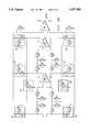
- FIG. 1Ais a schematic diagram of a single-ended switched-capacitor integrator according to the present invention.
- the switched-capacitor integrator 10includes a chopper stabilized differential operational amplifier 12, a feedback capacitor 14 coupled between an output 16 of the amplifier 12 and a first input 18 of the amplifier 12, with a second input 20 connected to signal ground.
- the amplifier 12has signal inputs FCHOP and FCHOP on lines 22 and 23, respectively, which are produced by circuitry not shown in the drawings.
- the output of the amplifier 12 on line 16is sampled by signal FSAMPLE shown by switch 24 to form the output signal VOUT at terminal 26.
- the switched-capacitor integrator 10receives an input signal VIN at input terminal 28 which is coupled through a first switch 30 to a node 32.
- Node 32is coupled to signal ground through a switch 34.
- Node 32is connected to one terminal of an input capacitor 36 the other terminal of which is connected to another node 38.
- Node 38is coupled to signal ground through a switch 40.
- Node 38is coupled to the input 18 of the amplifier 12 through another switch 42.
- the switches 30 and 40are controlled by timing signals ⁇ A, and the switches 34 and 38 are controlled by the timing signal ⁇ B.
- FIG. 1Bis a schematic diagram of the chopped amplifier 12 of FIG. 1A.
- the input 18is coupled to the minus input of an operational amplifier 42 through a switch 43 controlled by FCHOP and to the positive input of the operational amplifier 42 through a switch 43' controlled by FCHOP.
- the input 20is coupled to the minus input of an operational amplifier 42 through a switch 44' controlled by FCHOP and to the positive input of the operational amplifier 42 through a switch 44 controlled by FCHOP.
- the output of the operational amplifier 42is coupled to the output 16 of the chopped amplifier 12 through a noninverting amplifier 45 and a switch 47 controlled by FCHOP, and also through an inverting amplifier 46 and a switch 47' controlled by FCHOP.
- the chopped amplifier 12has a first chopping state and a second chopping state.
- the first chopping statewhen FCHOP is high and FCHOP is low, the switches 43, 44 and 47 are closed while the switches 43', 44' and 47' are open.
- the input 18is coupled to the minus input of the operational amplifier 42, the input 20 is coupled to the positive input of the operational amplifier 42, and the output of the operational amplifier 42 is coupled to the output 16.
- the second chopping statewhen FCHOP is low and FCHOP is high, the switches 43, 44 and 47 are open while the switches 43', 44' and 47' are closed.
- the input 18is coupled to the positive input of the operational amplifier 42
- the input 20is coupled to the minus input of the operational amplifier 42
- the output of the operational amplifier 42is inverted and coupled to the output 16.
- FIG. 1Cis a timing diagram for the circuit shown in FIG. 1A. As shown in FIG. 1C, for each sample of the output shown as FSAMPLE in FIG. 1C, there are two phases of the FCHOP and the FCHOP signals and four subphases of the ⁇ A and ⁇ B signals.
- FIG. 2Ais a diagram of FIG. 1A during subphase one of the operation
- FIG. 2Bis a schematic of FIG. 1A during subphase two
- FIG. 2Cis a schematic diagram during subphase three
- FIG. 2Dis a schematic diagram during subphase four.
- the amplifier 12has a negative input at input 18 and a positive input at input 20 and a positive output at the output 16, and the switches 30 and 40 are closed while the switches 34 and 42 are open.
- the input signal VINis sampled on the input capacitor 36 while the feedback capacitor 14 stores the voltage from subphase four of the previous cycle.
- subphase twoshown in FIG. 2B
- the input terminals 18 and 20 and the output terminal 16 of the amplifier 12remain unchanged in polarity and switches 34 and 42 are closed while switches 30 and 40 are open.
- a sampled input on capacitor 36is passed to the feedback capacitor 14.
- the amplifier noiseas represented by Vn if FIG. 2B, is sampled and subtracted from the feedback capacitor 14.
- subphase threethe input 18 of the amplifier 12 becomes a positive input, the input 20 becomes a negative input, and the output 16 becomes a negative output since the signals FCHOP and FCHOP change polarity. Also, at this time the switches 30, 34, 38, and 40 are in the same position they were during subphase one. Thus, during this third subphase, the input signal VIN is sampled on the input capacitor 36 while the voltage on the feedback capacitor 14 remains unchanged.
- subphase fourshown in FIG. 2D
- the inputs 18 and 20 and the output 16 of the amplifier 12remain unchanged from the third subphase, and the switches 30, 34, 40, and 42 are switched to the same position they are in subphase two.
- the sampled input on the input capacitor 36is added (transferred) to the feedback capacitor 14. Also, the inverse of the noise of the amplifier 12 is sampled and subtracted from the feedback capacitor 14. In this manner, the low frequency interference and the flicker noise of the amplifier 12 is removed from the output signal on the output terminal 26.
- the output of the switched-capacitor integrator 10is sampled during the first subphase by the closure of the switch 24. However, as will be shown below, since the output of the integrator 24 is the same during the fourth subphase and the first subphase of the next cycle, the sampling can also occur during the fourth subphase.
- the switched-capacitor integrator 10 of FIG. 1Ais a double-sampled integrator. Also, since the chopping clocks FCHOP and FCHOP are the same frequency as the sampling signal FSAMPLE, then the input signal VIN is sampled at twice the frequency as the output sample FSAMPLE.
- FIG. 3Ais a plot of the input referred transfer function of the amplifier shown in FIG. 1A
- FIG. 3Bis a plot of the noise input referred transfer function of the amplifier shown in FIG. 1A.
- the voltage at the end of sample nis equal to the voltage at the end of sample n-1 plus the voltage from the end of the first subphase (which occurs at n-3/4) plus the voltage at the end of the second subphase (which occurs at n-1/2) plus the voltage at the end of the third subphase (which occurs at n-1/4) plus the incremental voltage at the end of the fourth subphase (which occurs at n).
- subphase 1For subphase 1:
- the ##EQU6## term in the input and noise transfer functionsis the familiar discrete-time integrator.
- the numerators of these transfer functionsis what determines their input referred response. Their steady state response is shown in FIGS. 3A and 3B respectively. Note that the noise transfer function has a zero at DC.
- FIG. 4Ais a schematic diagram of a fully differential version of the switched-capacitor integrator shown in FIG. 1A.
- This fully differential versionwhich utilizes a fully differential chopped amplifier 48, is the preferred embodiment of the present invention.
- the circuit shown in FIG. 4Aoperates according to the same principles described above with respect to the circuit shown in FIG. 1A, and the timing of the switches shown is FIG. 4A is the same timing shown in FIG. 1C.
- FIG. 5is a plot of the input referred input transfer function of the circuit shown in FIG. 4A.
- the curve shown in FIG. 3Bis applicable to the circuit shown in FIG. 4A.
- FIG. 4Bis a schematic diagram of the chopped amplifier shown in FIG. 4A.
- an operational amplifier 49has minus and plus inputs which are switched in the same manner as the chopped amplifier shown in FIG. 1B.
- the positive and negative outputs of the amplifier 49are switched by switches 50 and 51, controlled by the FCHOP signal, and switches 50' and 51' controlled by the FCHOP signal.
- FIG. 4Cis an alternate embodiment of a fully differential switched-capacitor integrator according to the present invention.
- each of the first terminals of the input capacitors, CIare alternatively connected between an input signal (VINP or VINM) and signal ground rather than between one input signal and the other input signal as shown in FIG. 4A.
- FIG. 6is a block diagram of a delta-sigma converter 52 which includes a switched-capacitor integrator according to the present invention.
- the input signal VINis connected to the positive input of a summing circuit 53.
- the output of the summing circuitis connected to the input of the switched-capacitor integrator 10.
- the output of the switched-capacitor integrator 10is connected to an input of a block 54 of conventional switched-capacitor integrators to form the rest of the analog loop filter.
- the output of the block 54 of conventional switched-capacitor integratorsis connected to the input of a quantizer 55 the output of which forms the digital output signal DOUT.
- the DOUT signalis connected to the input of a D/A converter 56, the output of which is connected to the minus input of the summing circuit 50.
- the input signal VINis summed with an analog signal produced by the D/A converter 56 in the summing circuit 53 and this sum is connected to the input of the switched-capacitor integrator 10.
- Only the first integrator 10is double-sampled since the later integrators do not contribute significant low frequency noise.
- this switched-capacitor integrator 10provides effective attenuation of the low frequency noise interference of the amplifier 12, and since the double-sampled integrator 10 is chopped at the modulator sampling rate, the tone mechanisms which occur when the integrator is chopped at one-half the sampling rate are eliminated.
- the output of the switched-capacitor integrator 10is then further filtered by the conventional switched-capacitor integrator block 54 and the output of this switched-capacitor integrator block 54 is quantized in the quantizer 55 to form the output signal DOUT.
- the output of the quantizer 55is converted to an analog signal in the D/A converter 56.
- the output signal DOUTis conventionally coupled to the input of a digital decimation filter which converts the oversampled serial bitstream of DOUT into a conventional digital signal and which also provides filtering of DOUT.
- FIG. 7is a block diagram of an instrumentation amplifier which utilizes the present invention.
- two differential input signals AINP and AINMare connected to the positive inputs of two chopper-stabilized differential amplifiers 60 and 62 respectively.
- the negative inputs of the amplifiers 60 and 62are coupled together through a resistor 64 and the output of the amplifier 60 is connected to its negative input through a feedback resistor 66.
- the output of the operational amplifier 62is connected to its negative input through feedback resistor 68.
- the output of the amplifier 60is connected to the AIN+ input of a differential double-sampled delta-sigma converter 70.
- the amplifier 62is connected to the AIN- input of the delta-sigma converter 70.
- the amplifiers 60 and 62are chopped at the sampling frequency of the delta-sigma converter 70.
- the chopper stabilized amplifiers 60 and 62modulate the flicker noise and low frequency interference to odd harmonics of the chopping frequency, which is the same as the sampling frequency, and the switched-capacitor integrator of the first filter stage of the delta-sigma converter 70 suppresses this modulated noise and interference since the input referred transfer function of the switch-capacitor integrator has nulls at odd harmonics of the sampling frequency as shown in FIG. 3A.
- the amplifiers 60 and 62also provide a high input impedance to the input signals AINP and AINM.
- the present inventionis also applicable to FIG. 7 when none of the stages of the delta-sigma converter 70 are chopper stabilized. That is the modulated noise is suppressed in the delta-sigma converter 70 when the sample frequency of the delta-sigma converter 70 is equal to the chopping frequency of the chopper-stabilized differential amplifiers 60 and 62 (or equal to the chopping frequency divided by a positive integer), and the input sampling frequency of the delta-sigma converter 70 is twice the chopping frequency of the chopper-stabilized differential amplifiers 60 and 62.
- FIG. 8is a block diagram of the delta-sigma converter 70 shown in FIG. 7.
- the input signal AINis connected to a positive input of a summing circuit or adder 78.
- the input AIN in FIG. 8represents the differential input signals AIN+ and AIN- of FIG. 7.
- the output of the adder 78is connected to the input of a first integrator stage 80, the output of which is connected to the positive input of a second adder 82.
- the output of the adder 82is connected to the input of a second integrator 84, the output of which is connected to the input of a third integrator 86.
- the output of the integrator 86is coupled to the input of a feedback element 88 shown as B.
- the output of the feedback element 88is connected to the negative input of the adder 82.
- the output of the integrator 80is connected to the input of a feedforward element 90, shown as A 1 .
- the output of the integrator 84is connected to the input of a second feedforward element 92 shown as A 2 .
- the output of the integrator 86is connected to the input of a third feedforward element 94 shown as A 3 .
- the outputs from the three feedforward elements 90, 91, and 92are added together at an adder 96 and the output of the adder 96 is connected to the positive input of a quantizer or comparator 98.
- the negative input at the comparator 98is shown connected to signal ground for purposes of this block diagram representation of the preferred embodiment.
- the output of the comparator 98forms the output signal DOUT.
- the output of the comparator 98also is used to control a switch 100 which selects between a positive reference voltage, VREF+, and a negative reference voltage, VREF-, to be connected to the negative input of the adder 78.
- the delta-sigma modulator 70 shown in FIG. 8is a third order modulator which operates according to the principles well known to those skilled in the delta-sigma modulators.
- FIGS. 9A and 9Bform a schematic diagram of the delta-sigma modulator 70 shown in FIG. 8.
- the input signals AIN+ and AIN-are cross coupled before the first capacitor elements in the manner shown in FIG. 4A. These are cross coupled by switches shown in block 102.
- the operational amplifiers 104, 106, and 108 of FIGS. 9A and 9Bform the active elements of the integrators 80, 84, and 86, respectively, shown in FIG. 8.
- the feedback element 88 in FIG. 8is a differential feedback element in FIG. 9B, shown as elements 88' and 88".
- the feed forward elements 90, 92, and 94are shown as elements 90' and 90", 92' and 92", and 94' and 94" respectively in FIG. 9B.
- FIG. 10is a timing diagram of the switches shown in FIG. 9A and 9B.
- the arrowsindicate the sequence of switching at the phase boundaries of the signals S1-S4 and SA-SD.
- the signal FCHOPis the chopping signal used to chop, or switch, the inputs and outputs of the operational amplifier 104, and the instrumentation amplifiers 60 and 62.
- the integrator 80is a discrete time integrator in which the operational amplifier 104 is chopped at the sampling frequency. This ability to chop at the sample rate in a discrete time circuit arises from the timing signals S1-S4 which double sample the input signal at a rate which is twice the sample rate of the modulator. This circuit then takes advantage of the flicker and low frequency interference rejection of a chopper stabilized amplifier without introducing tones or requiring a continuous time integrator to precede the discrete time integrator.
- FIG. 11Ais the schematic diagram of the preferred embodiment of the chopped amplifier 104 shown in FIG. 9A.
- the differential input signals INP and INMare switched at the input of the amplifier 104 by timing signals CH3 and CH4.
- the differential outputs of the amplifier 104are also switched by timing signals CH1 and CH2.
- the amplifier itselfis of a design well know in the art with B1-B6 being bias voltages, and B1CM being a bias voltage driven by a common mode amplifier (not shown) which receives VOUTP and VOUTN as input signals.
- B1CMoperates to keep the common mode output of the amplifier at substantially half way between VDD and VSS.
- FIG. 11Bshows the timing relationships of CH1-CH4 in relation to FCHOP which is also shown in FIG. 10.
Landscapes
- Engineering & Computer Science (AREA)
- Physics & Mathematics (AREA)
- Theoretical Computer Science (AREA)
- Mathematical Physics (AREA)
- General Physics & Mathematics (AREA)
- Power Engineering (AREA)
- Software Systems (AREA)
- Computer Hardware Design (AREA)
- Amplifiers (AREA)
- Filters That Use Time-Delay Elements (AREA)
Abstract
Description
VOUT(n-3/4)=VOUT(n-1) (1)
VOUT(n -1/4)=VOUT(n-1/2) (3)
VOUT(n-3/4)=VOUT(n-1) (9)
VOUT(n-1/4)=VOUT(n-1/2) (11)
Claims (18)
Priority Applications (1)
| Application Number | Priority Date | Filing Date | Title |
|---|---|---|---|
| US08/221,985US5477481A (en) | 1991-02-15 | 1994-04-01 | Switched-capacitor integrator with chopper stabilization performed at the sampling rate |
Applications Claiming Priority (3)
| Application Number | Priority Date | Filing Date | Title |
|---|---|---|---|
| US65629491A | 1991-02-15 | 1991-02-15 | |
| US71128791A | 1991-06-06 | 1991-06-06 | |
| US08/221,985US5477481A (en) | 1991-02-15 | 1994-04-01 | Switched-capacitor integrator with chopper stabilization performed at the sampling rate |
Related Parent Applications (1)
| Application Number | Title | Priority Date | Filing Date |
|---|---|---|---|
| US71128791AContinuation | 1991-02-15 | 1991-06-06 |
Publications (1)
| Publication Number | Publication Date |
|---|---|
| US5477481Atrue US5477481A (en) | 1995-12-19 |
Family
ID=27097166
Family Applications (1)
| Application Number | Title | Priority Date | Filing Date |
|---|---|---|---|
| US08/221,985Expired - LifetimeUS5477481A (en) | 1991-02-15 | 1994-04-01 | Switched-capacitor integrator with chopper stabilization performed at the sampling rate |
Country Status (1)
| Country | Link |
|---|---|
| US (1) | US5477481A (en) |
Cited By (101)
| Publication number | Priority date | Publication date | Assignee | Title |
|---|---|---|---|---|
| US5982315A (en)* | 1997-09-12 | 1999-11-09 | Qualcomm Incorporated | Multi-loop Σ Δ analog to digital converter |
| US6002299A (en)* | 1997-06-10 | 1999-12-14 | Cirrus Logic, Inc. | High-order multipath operational amplifier with dynamic offset reduction, controlled saturation current limiting, and current feedback for enhanced conditional stability |
| US6005506A (en)* | 1997-12-09 | 1999-12-21 | Qualcomm, Incorporated | Receiver with sigma-delta analog-to-digital converter for sampling a received signal |
| US6169440B1 (en) | 1999-03-10 | 2001-01-02 | National Science Council | Offset-compensated switched-opamp integrator and filter |
| US6191648B1 (en) | 1999-04-19 | 2001-02-20 | National Semiconductor Corporation | Switched-capacitor cosine filter circuit |
| US6201835B1 (en) | 1999-03-05 | 2001-03-13 | Burr-Brown Corporation | Frequency-shaped pseudo-random chopper stabilization circuit and method for delta-sigma modulator |
| US6259313B1 (en)* | 1999-04-19 | 2001-07-10 | National Semiconductor Corporation | Chopper-stabilized telescopic differential amplifier |
| US6285311B1 (en) | 1999-04-19 | 2001-09-04 | National Semiconductor Corporation | Switched capacitor filter circuit having reduced offsets and allowing for offset compensation without a closed feedback loop |
| US6307430B1 (en) | 2000-10-02 | 2001-10-23 | Cirrus Logic, Inc. | Noise reduction technique in chopper stabilized amplifier |
| EP1172936A1 (en)* | 2000-07-11 | 2002-01-16 | STMicroelectronics S.r.l. | Digital to analogue converter comprising a third order sigma delta modulator |
| US6351506B1 (en) | 1999-04-19 | 2002-02-26 | National Semiconductor Corporation | Switched capacitor filter circuit having reduced offsets and providing offset compensation when used in a closed feedback loop |
| US6466091B1 (en) | 2000-10-02 | 2002-10-15 | Cirrus Logic, Inc. | High order multi-path operational amplifier with reduced input referred offset |
| US6498926B1 (en) | 1997-12-09 | 2002-12-24 | Qualcomm Incorporated | Programmable linear receiver having a variable IIP3 point |
| US6515540B1 (en) | 2001-12-10 | 2003-02-04 | Cirrus Logic, Inc. | High order multi-path operational amplifier with output saturation recovery |
| US6639532B1 (en)* | 2002-07-16 | 2003-10-28 | Macronix International Co., Ltd. | Nested chopper delta-sigma modulator |
| US20040141562A1 (en)* | 2003-01-21 | 2004-07-22 | Plisch Marjorie R. | Signal processing system with baseband noise modulaltion chopper circuit timing to reduce noise |
| US20040169529A1 (en)* | 2000-02-02 | 2004-09-02 | Afghahi Morteza Cyrus | Single-ended sense amplifier with sample-and-hold reference |
| EP1164707A3 (en)* | 2000-05-15 | 2004-12-01 | Texas Instruments Inc. | Attentuating undesired frequencies while sampling a communication signal |
| US6870495B1 (en)* | 2004-02-18 | 2005-03-22 | Micron Technology, Inc. | Double throughput analog to digital converter |
| US20050156769A1 (en)* | 2004-01-15 | 2005-07-21 | O'dowd John | Reduced chop rate analog to digital converter system and method |
| US20050237089A1 (en)* | 2004-04-26 | 2005-10-27 | Daniel Van Blerkom | Method and circuit thereof for smapling/holding signal |
| US20060244521A1 (en)* | 2005-03-29 | 2006-11-02 | Takeshi Yoshida | Chopper amplifier circuit apparatus operable at low voltage utilizing switched operational amplifier |
| US7167119B1 (en)* | 2005-12-20 | 2007-01-23 | Cirrus Logic, Inc. | Delta-sigma modulators with double sampling input networks and systems using the same |
| US7170338B1 (en) | 2005-03-24 | 2007-01-30 | Cirrus Logic, Inc. | Chopper stabilization circuits and methods |
| US20070115049A1 (en)* | 2005-11-09 | 2007-05-24 | Chang-Shun Liu | Operational amplifier and related noise separation method thereof |
| US20080106330A1 (en)* | 2006-09-07 | 2008-05-08 | Takeshi Yoshida | Feedback amplifier circuit operable at low voltage by utilizing switched operational amplifier and chopper modulator |
| US7385443B1 (en) | 2007-01-31 | 2008-06-10 | Medtronic, Inc. | Chopper-stabilized instrumentation amplifier |
| US7391257B1 (en) | 2007-01-31 | 2008-06-24 | Medtronic, Inc. | Chopper-stabilized instrumentation amplifier for impedance measurement |
| US20080174372A1 (en)* | 2007-01-19 | 2008-07-24 | Tucker John C | Multi-stage amplifier with multiple sets of fixed and variable voltage rails |
| US20080180278A1 (en)* | 2007-01-31 | 2008-07-31 | Medtronic, Inc. | Chopper-stabilized instrumentation amplifier for wireless telemetry |
| US20080269630A1 (en)* | 2007-04-30 | 2008-10-30 | Medtronic, Inc. | Seizure prediction |
| US20080269631A1 (en)* | 2007-04-30 | 2008-10-30 | Medtronic, Inc. | Seizure prediction |
| US20080269841A1 (en)* | 2007-04-30 | 2008-10-30 | Medtronic, Inc. | Chopper mixer telemetry circuit |
| US20080272744A1 (en)* | 2007-05-02 | 2008-11-06 | Cirrus Logic, Inc. | Power control system using a nonlinear delta-sigma modulator with nonlinear power conversion process modeling |
| US20080272946A1 (en)* | 2007-05-02 | 2008-11-06 | Melanson John L | Signal processing system using delta-sigma modulation having an internal stabilizer path with direct output-to-integrator connection |
| EP2009795A1 (en)* | 2007-06-29 | 2008-12-31 | Fujitsu Ltd. | Low noise electronic circuitry |
| US20090079607A1 (en)* | 2007-09-26 | 2009-03-26 | Medtronic, Inc. | Chopper-stabilized analog-to-digital converter |
| US20090079606A1 (en)* | 2007-09-26 | 2009-03-26 | Terry Michael B | Implantable medical device with low power delta-sigma analog-to-digital converter |
| US20090082691A1 (en)* | 2007-09-26 | 2009-03-26 | Medtronic, Inc. | Frequency selective monitoring of physiological signals |
| US20090108461A1 (en)* | 2007-10-31 | 2009-04-30 | Hynix Semiconductor Inc. | Semiconductor device and method of fabricating the same |
| US20090167580A1 (en)* | 2007-12-28 | 2009-07-02 | Andrew Hutchinson | Sigma delta analog to digital converter with internal synchronous demodulation |
| US20090191837A1 (en)* | 2008-01-30 | 2009-07-30 | Kartik Nanda | Delta Sigma Modulator with Unavailable Output Values |
| US20090189579A1 (en)* | 2008-01-30 | 2009-07-30 | Melanson John L | Switch state controller with a sense current generated operating voltage |
| US20090190384A1 (en)* | 2008-01-30 | 2009-07-30 | Cirrus Logic, Inc. | Powering a power supply integrated circuit with sense current |
| US7667408B2 (en) | 2007-03-12 | 2010-02-23 | Cirrus Logic, Inc. | Lighting system with lighting dimmer output mapping |
| US20100113964A1 (en)* | 2008-10-31 | 2010-05-06 | Wahlstrand John D | Determining intercardiac impedance |
| US20100156319A1 (en)* | 2008-08-29 | 2010-06-24 | John Laurence Melanson | LED Lighting System with Accurate Current Control |
| US20100164406A1 (en)* | 2008-07-25 | 2010-07-01 | Kost Michael A | Switching power converter control with triac-based leading edge dimmer compatibility |
| US20100164631A1 (en)* | 2008-12-31 | 2010-07-01 | Cirrus Logic, Inc. | Electronic system having common mode voltage range enhancement |
| US20100171442A1 (en)* | 2008-12-12 | 2010-07-08 | Draper William A | Light Emitting Diode Based Lighting System With Time Division Ambient Light Feedback Response |
| US7759881B1 (en) | 2008-03-31 | 2010-07-20 | Cirrus Logic, Inc. | LED lighting system with a multiple mode current control dimming strategy |
| US7804256B2 (en) | 2007-03-12 | 2010-09-28 | Cirrus Logic, Inc. | Power control system for current regulated light sources |
| US7804697B2 (en) | 2007-12-11 | 2010-09-28 | Cirrus Logic, Inc. | History-independent noise-immune modulated transformer-coupled gate control signaling method and apparatus |
| US20100244726A1 (en)* | 2008-12-07 | 2010-09-30 | Melanson John L | Primary-side based control of secondary-side current for a transformer |
| US20100277072A1 (en)* | 2009-04-30 | 2010-11-04 | Draper William A | Calibration Of Lamps |
| US20100295529A1 (en)* | 2009-05-22 | 2010-11-25 | Linear Technology Corporation | Chopper stabilized bandgap reference circuit and methodology for voltage regulators |
| US20100328976A1 (en)* | 2009-06-30 | 2010-12-30 | Melanson John L | Cascode configured switching using at least one low breakdown voltage internal, integrated circuit switch to control at least one high breakdown voltage external switch |
| US20110063146A1 (en)* | 2009-09-15 | 2011-03-17 | Texas Instruments Incorporated | Multistage chopper stabilized delta-sigma adc with reduced offset |
| US20110074302A1 (en)* | 2009-09-30 | 2011-03-31 | Draper William A | Phase Control Dimming Compatible Lighting Systems |
| US8008902B2 (en) | 2008-06-25 | 2011-08-30 | Cirrus Logic, Inc. | Hysteretic buck converter having dynamic thresholds |
| US8008898B2 (en) | 2008-01-30 | 2011-08-30 | Cirrus Logic, Inc. | Switching regulator with boosted auxiliary winding supply |
| US8014176B2 (en) | 2008-07-25 | 2011-09-06 | Cirrus Logic, Inc. | Resonant switching power converter with burst mode transition shaping |
| US8018171B1 (en) | 2007-03-12 | 2011-09-13 | Cirrus Logic, Inc. | Multi-function duty cycle modifier |
| US8072262B1 (en)* | 2010-06-28 | 2011-12-06 | Texas Instruments Incorporated | Low input bias current chopping switch circuit and method |
| EP2378660A3 (en)* | 2010-04-14 | 2011-12-07 | Rolls-Royce Goodrich Engine Control Systems Ltd. | A Signal Processing Circuit |
| US8076920B1 (en) | 2007-03-12 | 2011-12-13 | Cirrus Logic, Inc. | Switching power converter and control system |
| US8102127B2 (en) | 2007-06-24 | 2012-01-24 | Cirrus Logic, Inc. | Hybrid gas discharge lamp-LED lighting system |
| US8179110B2 (en) | 2008-09-30 | 2012-05-15 | Cirrus Logic Inc. | Adjustable constant current source with continuous conduction mode (“CCM”) and discontinuous conduction mode (“DCM”) operation |
| US8198874B2 (en) | 2009-06-30 | 2012-06-12 | Cirrus Logic, Inc. | Switching power converter with current sensing transformer auxiliary power supply |
| US8212493B2 (en) | 2009-06-30 | 2012-07-03 | Cirrus Logic, Inc. | Low energy transfer mode for auxiliary power supply operation in a cascaded switching power converter |
| US8222872B1 (en) | 2008-09-30 | 2012-07-17 | Cirrus Logic, Inc. | Switching power converter with selectable mode auxiliary power supply |
| US8299722B2 (en) | 2008-12-12 | 2012-10-30 | Cirrus Logic, Inc. | Time division light output sensing and brightness adjustment for different spectra of light emitting diodes |
| US20120306575A1 (en)* | 2011-06-06 | 2012-12-06 | Qualcomm Incorporated | Switched-capacitor dc blocking amplifier |
| US8344707B2 (en) | 2008-07-25 | 2013-01-01 | Cirrus Logic, Inc. | Current sensing in a switching power converter |
| US20130036147A1 (en)* | 2011-08-02 | 2013-02-07 | Mediatek Inc. | Infinite impulse response (iir) filter and filtering method |
| CN103138760A (en)* | 2012-11-05 | 2013-06-05 | 戴祖渝 | Amplifier with ultralow direct current (DC) offset at input end and analog/digital (A/D) converter |
| US8471744B1 (en) | 2011-12-01 | 2013-06-25 | Hong Kong Applied Science & Technology Research Institute Company, Ltd. | Reduced residual offset sigma delta analog-to-digital converter (ADC) with chopper timing at end of integrating phase before trailing edge |
| US8478402B2 (en) | 2008-10-31 | 2013-07-02 | Medtronic, Inc. | Determining intercardiac impedance |
| US8554325B2 (en) | 2007-10-16 | 2013-10-08 | Medtronic, Inc. | Therapy control based on a patient movement state |
| US20140042999A1 (en)* | 2012-08-10 | 2014-02-13 | Texas Instruments Incorporated | Switched mode assisted linear regulator with ac coupling with capacitive charge control |
| US8654483B2 (en) | 2009-11-09 | 2014-02-18 | Cirrus Logic, Inc. | Power system having voltage-based monitoring for over current protection |
| WO2014149980A1 (en)* | 2013-03-15 | 2014-09-25 | Medtronic, Inc. | Control of spectral agressors in a physiological signal monitoring device |
| US8963535B1 (en) | 2009-06-30 | 2015-02-24 | Cirrus Logic, Inc. | Switch controlled current sensing using a hall effect sensor |
| CN104682945A (en)* | 2013-08-15 | 2015-06-03 | 德州仪器德国股份有限公司 | Fluxgate Magnetic Sensor Readout Device |
| US20150155783A1 (en)* | 2012-08-10 | 2015-06-04 | Texas Instruments Incorporated | Switched mode assisted linear regulator with dynamic buck turn-off using zcd-controlled tub switching |
| US9248288B2 (en) | 2007-09-26 | 2016-02-02 | Medtronic, Inc. | Patient directed therapy control |
| US9439150B2 (en) | 2013-03-15 | 2016-09-06 | Medtronic, Inc. | Control of spectral agressors in a physiological signal montoring device |
| US9473023B2 (en) | 2012-08-10 | 2016-10-18 | Texas Instruments Incorporated | Switched mode assisted linear regulator with seamless transition between power tracking configurations |
| US9615744B2 (en) | 2007-01-31 | 2017-04-11 | Medtronic, Inc. | Chopper-stabilized instrumentation amplifier for impedance measurement |
| US9706957B2 (en) | 2008-01-25 | 2017-07-18 | Medtronic, Inc. | Sleep stage detection |
| US9770204B2 (en) | 2009-11-11 | 2017-09-26 | Medtronic, Inc. | Deep brain stimulation for sleep and movement disorders |
| CN107332563A (en)* | 2017-05-31 | 2017-11-07 | 苏州真感微电子科技有限公司 | Reduce the circuit of switching capacity input current and the method for sampling of switching capacity |
| US9924904B2 (en) | 2014-09-02 | 2018-03-27 | Medtronic, Inc. | Power-efficient chopper amplifier |
| CN109889198A (en)* | 2017-12-06 | 2019-06-14 | 美国亚德诺半导体公司 | The multi input data converter modulated using code |
| US20200162092A1 (en)* | 2017-10-27 | 2020-05-21 | Analog Devices, Inc. | Track and hold circuits for high speed and interleaved adcs |
| US10666278B2 (en)* | 2018-03-16 | 2020-05-26 | Asahi Kasei Microdevices Corporation | DA converter and DA conversion method |
| US10873336B2 (en) | 2017-10-27 | 2020-12-22 | Analog Devices, Inc. | Track and hold circuits for high speed and interleaved ADCs |
| TWI742259B (en)* | 2017-03-31 | 2021-10-11 | 日商艾普凌科有限公司 | Differential amplifier |
| US11177821B1 (en) | 2020-08-11 | 2021-11-16 | Analog Devices, Inc. | Analog-to-digital converter with auto-zeroing residue amplification circuit |
| US12073269B2 (en) | 2021-01-28 | 2024-08-27 | Analog Devices International Unlimited Company | Switched-capacitor integrators with improved flicker noise rejection |
| US12334875B2 (en) | 2019-08-29 | 2025-06-17 | Semiconductor Energy Laboratory Co., Ltd. | Semiconductor device and operation method thereof |
Citations (14)
| Publication number | Priority date | Publication date | Assignee | Title |
|---|---|---|---|---|
| US4746899A (en)* | 1986-10-07 | 1988-05-24 | Crystal Semiconductor Corporation | Method for reducing effects of electrical noise in an analog-to-digital converter |
| US4803650A (en)* | 1985-04-08 | 1989-02-07 | Sony Corporation | Method of configuring an n- th degree switched capacitor filter |
| US4912423A (en)* | 1989-02-27 | 1990-03-27 | General Electric Company | Chopper-stabilized operational transconductance amplifier |
| US4939516A (en)* | 1988-06-13 | 1990-07-03 | Crystal Semiconductor | Chopper stabilized delta-sigma analog-to-digital converter |
| US4994805A (en)* | 1988-08-05 | 1991-02-19 | The General Electric Company, P.L.C. | Delta sigma modulator arrangements compensated by chopper stabilization |
| US4999634A (en)* | 1989-05-08 | 1991-03-12 | Siemens Aktiengesellschaft | Integratable switched-capacitor sigma-delta modulator |
| US5039989A (en)* | 1989-10-27 | 1991-08-13 | Crystal Semiconductor Corporation | Delta-sigma analog-to-digital converter with chopper stabilization at the sampling frequency |
| US5057839A (en)* | 1989-05-08 | 1991-10-15 | Siemens Aktiengesellschaft | Integratable switched-capacitor sigma-delta modulator |
| US5072219A (en)* | 1989-02-07 | 1991-12-10 | Texas Instruments Incorporated | Digital-analog conversion system including a digital modulator having several quantification levels, associated with a digital-analog converter |
| US5079550A (en)* | 1989-10-27 | 1992-01-07 | Crystal Semiconductor Corporation | Combining continuous time and discrete time signal processing in a delta-sigma modulator |
| US5148167A (en)* | 1990-04-06 | 1992-09-15 | General Electric Company | Sigma-delta oversampled analog-to-digital converter network with chopper stabilization |
| US5148166A (en)* | 1990-04-06 | 1992-09-15 | General Electric Company | Third order sigma delta oversampled analog-to-digital converter network with low component sensitivity |
| US5159341A (en)* | 1991-03-12 | 1992-10-27 | Analog Devices, Inc. | Two phase sampling for a delta sigma modulator |
| US5168461A (en)* | 1989-08-21 | 1992-12-01 | Industrial Technology Research Institute | Switched capacitor differentiators and switched capacitor differentiator-based filters |
- 1994
- 1994-04-01USUS08/221,985patent/US5477481A/ennot_activeExpired - Lifetime
Patent Citations (15)
| Publication number | Priority date | Publication date | Assignee | Title |
|---|---|---|---|---|
| US4803650A (en)* | 1985-04-08 | 1989-02-07 | Sony Corporation | Method of configuring an n- th degree switched capacitor filter |
| US4746899A (en)* | 1986-10-07 | 1988-05-24 | Crystal Semiconductor Corporation | Method for reducing effects of electrical noise in an analog-to-digital converter |
| US4939516A (en)* | 1988-06-13 | 1990-07-03 | Crystal Semiconductor | Chopper stabilized delta-sigma analog-to-digital converter |
| US4939516B1 (en)* | 1988-06-13 | 1993-10-26 | Crystal Semiconductor Corporation | Chopper stabilized delta-sigma analog-to-digital converter |
| US4994805A (en)* | 1988-08-05 | 1991-02-19 | The General Electric Company, P.L.C. | Delta sigma modulator arrangements compensated by chopper stabilization |
| US5072219A (en)* | 1989-02-07 | 1991-12-10 | Texas Instruments Incorporated | Digital-analog conversion system including a digital modulator having several quantification levels, associated with a digital-analog converter |
| US4912423A (en)* | 1989-02-27 | 1990-03-27 | General Electric Company | Chopper-stabilized operational transconductance amplifier |
| US4999634A (en)* | 1989-05-08 | 1991-03-12 | Siemens Aktiengesellschaft | Integratable switched-capacitor sigma-delta modulator |
| US5057839A (en)* | 1989-05-08 | 1991-10-15 | Siemens Aktiengesellschaft | Integratable switched-capacitor sigma-delta modulator |
| US5168461A (en)* | 1989-08-21 | 1992-12-01 | Industrial Technology Research Institute | Switched capacitor differentiators and switched capacitor differentiator-based filters |
| US5039989A (en)* | 1989-10-27 | 1991-08-13 | Crystal Semiconductor Corporation | Delta-sigma analog-to-digital converter with chopper stabilization at the sampling frequency |
| US5079550A (en)* | 1989-10-27 | 1992-01-07 | Crystal Semiconductor Corporation | Combining continuous time and discrete time signal processing in a delta-sigma modulator |
| US5148166A (en)* | 1990-04-06 | 1992-09-15 | General Electric Company | Third order sigma delta oversampled analog-to-digital converter network with low component sensitivity |
| US5148167A (en)* | 1990-04-06 | 1992-09-15 | General Electric Company | Sigma-delta oversampled analog-to-digital converter network with chopper stabilization |
| US5159341A (en)* | 1991-03-12 | 1992-10-27 | Analog Devices, Inc. | Two phase sampling for a delta sigma modulator |
Cited By (174)
| Publication number | Priority date | Publication date | Assignee | Title |
|---|---|---|---|---|
| US6002299A (en)* | 1997-06-10 | 1999-12-14 | Cirrus Logic, Inc. | High-order multipath operational amplifier with dynamic offset reduction, controlled saturation current limiting, and current feedback for enhanced conditional stability |
| US5982315A (en)* | 1997-09-12 | 1999-11-09 | Qualcomm Incorporated | Multi-loop Σ Δ analog to digital converter |
| US6498926B1 (en) | 1997-12-09 | 2002-12-24 | Qualcomm Incorporated | Programmable linear receiver having a variable IIP3 point |
| US6005506A (en)* | 1997-12-09 | 1999-12-21 | Qualcomm, Incorporated | Receiver with sigma-delta analog-to-digital converter for sampling a received signal |
| US6201835B1 (en) | 1999-03-05 | 2001-03-13 | Burr-Brown Corporation | Frequency-shaped pseudo-random chopper stabilization circuit and method for delta-sigma modulator |
| US6169440B1 (en) | 1999-03-10 | 2001-01-02 | National Science Council | Offset-compensated switched-opamp integrator and filter |
| US6259313B1 (en)* | 1999-04-19 | 2001-07-10 | National Semiconductor Corporation | Chopper-stabilized telescopic differential amplifier |
| US6285311B1 (en) | 1999-04-19 | 2001-09-04 | National Semiconductor Corporation | Switched capacitor filter circuit having reduced offsets and allowing for offset compensation without a closed feedback loop |
| US6351506B1 (en) | 1999-04-19 | 2002-02-26 | National Semiconductor Corporation | Switched capacitor filter circuit having reduced offsets and providing offset compensation when used in a closed feedback loop |
| US6191648B1 (en) | 1999-04-19 | 2001-02-20 | National Semiconductor Corporation | Switched-capacitor cosine filter circuit |
| US8164362B2 (en)* | 2000-02-02 | 2012-04-24 | Broadcom Corporation | Single-ended sense amplifier with sample-and-hold reference |
| US20040169529A1 (en)* | 2000-02-02 | 2004-09-02 | Afghahi Morteza Cyrus | Single-ended sense amplifier with sample-and-hold reference |
| EP1164707A3 (en)* | 2000-05-15 | 2004-12-01 | Texas Instruments Inc. | Attentuating undesired frequencies while sampling a communication signal |
| US6483449B2 (en) | 2000-07-11 | 2002-11-19 | Stmicroelectronics S.R.L. | Digital-analog converter comprising a third order sigma delta modulator |
| EP1172936A1 (en)* | 2000-07-11 | 2002-01-16 | STMicroelectronics S.r.l. | Digital to analogue converter comprising a third order sigma delta modulator |
| US6466091B1 (en) | 2000-10-02 | 2002-10-15 | Cirrus Logic, Inc. | High order multi-path operational amplifier with reduced input referred offset |
| US6307430B1 (en) | 2000-10-02 | 2001-10-23 | Cirrus Logic, Inc. | Noise reduction technique in chopper stabilized amplifier |
| US6515540B1 (en) | 2001-12-10 | 2003-02-04 | Cirrus Logic, Inc. | High order multi-path operational amplifier with output saturation recovery |
| US6639532B1 (en)* | 2002-07-16 | 2003-10-28 | Macronix International Co., Ltd. | Nested chopper delta-sigma modulator |
| WO2004066642A2 (en) | 2003-01-21 | 2004-08-05 | Cirrus Logic Inc. | Signal processing system with baseband noise modulation chopper circuit timing to reduce noise |
| US20040141562A1 (en)* | 2003-01-21 | 2004-07-22 | Plisch Marjorie R. | Signal processing system with baseband noise modulaltion chopper circuit timing to reduce noise |
| WO2004066642A3 (en)* | 2003-01-21 | 2005-01-13 | Cirrus Logic Inc | Signal processing system with baseband noise modulation chopper circuit timing to reduce noise |
| US6961385B2 (en)* | 2003-01-21 | 2005-11-01 | Cirrus Logic, Inc. | Signal processing system with baseband noise modulation chopper circuit timing to reduce noise |
| US20050156769A1 (en)* | 2004-01-15 | 2005-07-21 | O'dowd John | Reduced chop rate analog to digital converter system and method |
| US7098823B2 (en)* | 2004-01-15 | 2006-08-29 | Analog Devices, Inc. | Reduced chop rate analog to digital converter system and method |
| US6870495B1 (en)* | 2004-02-18 | 2005-03-22 | Micron Technology, Inc. | Double throughput analog to digital converter |
| US20050237089A1 (en)* | 2004-04-26 | 2005-10-27 | Daniel Van Blerkom | Method and circuit thereof for smapling/holding signal |
| US7292071B2 (en)* | 2004-04-26 | 2007-11-06 | Sunplus Technology Co., Ltd. | Method and circuit for sampling/holding a signal |
| US7170338B1 (en) | 2005-03-24 | 2007-01-30 | Cirrus Logic, Inc. | Chopper stabilization circuits and methods |
| US7336123B2 (en) | 2005-03-29 | 2008-02-26 | Semiconductor Technology Academic Research Center | Chopper amplifier circuit apparatus operable at low voltage utilizing switched operational amplifier |
| US20060244521A1 (en)* | 2005-03-29 | 2006-11-02 | Takeshi Yoshida | Chopper amplifier circuit apparatus operable at low voltage utilizing switched operational amplifier |
| US20070115049A1 (en)* | 2005-11-09 | 2007-05-24 | Chang-Shun Liu | Operational amplifier and related noise separation method thereof |
| US7489187B2 (en) | 2005-11-09 | 2009-02-10 | Realtek Semiconductor Corp. | Operational amplifier and related noise separation method thereof |
| US7167119B1 (en)* | 2005-12-20 | 2007-01-23 | Cirrus Logic, Inc. | Delta-sigma modulators with double sampling input networks and systems using the same |
| US7589587B2 (en)* | 2006-09-07 | 2009-09-15 | Semiconductor Technology Academic Research Center | Feedback amplifier circuit operable at low voltage by utilizing switched operational amplifier and chopper modulator |
| US20080106330A1 (en)* | 2006-09-07 | 2008-05-08 | Takeshi Yoshida | Feedback amplifier circuit operable at low voltage by utilizing switched operational amplifier and chopper modulator |
| US20080174372A1 (en)* | 2007-01-19 | 2008-07-24 | Tucker John C | Multi-stage amplifier with multiple sets of fixed and variable voltage rails |
| US8362838B2 (en) | 2007-01-19 | 2013-01-29 | Cirrus Logic, Inc. | Multi-stage amplifier with multiple sets of fixed and variable voltage rails |
| US20080211574A1 (en)* | 2007-01-31 | 2008-09-04 | Medtronic, Inc. | Chopper-stabilized instrumentation amplifier |
| US20110068861A1 (en)* | 2007-01-31 | 2011-03-24 | Medtronic, Inc. | Chopper-stabilized instrumentation amplifier |
| US7622988B2 (en) | 2007-01-31 | 2009-11-24 | Medtronic, Inc. | Chopper-stabilized instrumentation amplifier for impedance measurement |
| US7847628B2 (en) | 2007-01-31 | 2010-12-07 | Medtronic, Inc. | Chopper-stabilized instrumentation amplifier |
| US7385443B1 (en) | 2007-01-31 | 2008-06-10 | Medtronic, Inc. | Chopper-stabilized instrumentation amplifier |
| US20080183098A1 (en)* | 2007-01-31 | 2008-07-31 | Medtronic, Inc. | Chopper-stabilized instrumentation amplifier for impedance measurement |
| US9615744B2 (en) | 2007-01-31 | 2017-04-11 | Medtronic, Inc. | Chopper-stabilized instrumentation amplifier for impedance measurement |
| US8265769B2 (en) | 2007-01-31 | 2012-09-11 | Medtronic, Inc. | Chopper-stabilized instrumentation amplifier for wireless telemetry |
| US9197173B2 (en) | 2007-01-31 | 2015-11-24 | Medtronic, Inc. | Chopper-stabilized instrumentation amplifier for impedance measurement |
| US7391257B1 (en) | 2007-01-31 | 2008-06-24 | Medtronic, Inc. | Chopper-stabilized instrumentation amplifier for impedance measurement |
| US8354881B2 (en) | 2007-01-31 | 2013-01-15 | Medtronic, Inc. | Chopper-stabilized instrumentation amplifier |
| US20080180278A1 (en)* | 2007-01-31 | 2008-07-31 | Medtronic, Inc. | Chopper-stabilized instrumentation amplifier for wireless telemetry |
| US8018171B1 (en) | 2007-03-12 | 2011-09-13 | Cirrus Logic, Inc. | Multi-function duty cycle modifier |
| US8174204B2 (en) | 2007-03-12 | 2012-05-08 | Cirrus Logic, Inc. | Lighting system with power factor correction control data determined from a phase modulated signal |
| US8076920B1 (en) | 2007-03-12 | 2011-12-13 | Cirrus Logic, Inc. | Switching power converter and control system |
| US7852017B1 (en) | 2007-03-12 | 2010-12-14 | Cirrus Logic, Inc. | Ballast for light emitting diode light sources |
| US7804256B2 (en) | 2007-03-12 | 2010-09-28 | Cirrus Logic, Inc. | Power control system for current regulated light sources |
| US7667408B2 (en) | 2007-03-12 | 2010-02-23 | Cirrus Logic, Inc. | Lighting system with lighting dimmer output mapping |
| US8781595B2 (en) | 2007-04-30 | 2014-07-15 | Medtronic, Inc. | Chopper mixer telemetry circuit |
| US9449501B2 (en) | 2007-04-30 | 2016-09-20 | Medtronics, Inc. | Chopper mixer telemetry circuit |
| US9788750B2 (en) | 2007-04-30 | 2017-10-17 | Medtronic, Inc. | Seizure prediction |
| US8594779B2 (en) | 2007-04-30 | 2013-11-26 | Medtronic, Inc. | Seizure prediction |
| US20080269630A1 (en)* | 2007-04-30 | 2008-10-30 | Medtronic, Inc. | Seizure prediction |
| US20080269841A1 (en)* | 2007-04-30 | 2008-10-30 | Medtronic, Inc. | Chopper mixer telemetry circuit |
| US20080269631A1 (en)* | 2007-04-30 | 2008-10-30 | Medtronic, Inc. | Seizure prediction |
| US20080272757A1 (en)* | 2007-05-02 | 2008-11-06 | Cirrus Logic, Inc. | Power supply dc voltage offset detector |
| US7888922B2 (en) | 2007-05-02 | 2011-02-15 | Cirrus Logic, Inc. | Power factor correction controller with switch node feedback |
| US8120341B2 (en) | 2007-05-02 | 2012-02-21 | Cirrus Logic, Inc. | Switching power converter with switch control pulse width variability at low power demand levels |
| US7696913B2 (en)* | 2007-05-02 | 2010-04-13 | Cirrus Logic, Inc. | Signal processing system using delta-sigma modulation having an internal stabilizer path with direct output-to-integrator connection |
| US20080273356A1 (en)* | 2007-05-02 | 2008-11-06 | Melanson John L | Switching Power Converter with Efficient Switching Control Signal Period Generation |
| US8040703B2 (en) | 2007-05-02 | 2011-10-18 | Cirrus Logic, Inc. | Power factor correction controller with feedback reduction |
| US7719248B1 (en) | 2007-05-02 | 2010-05-18 | Cirrus Logic, Inc. | Discontinuous conduction mode (DCM) using sensed current for a switch-mode converter |
| US7719246B2 (en) | 2007-05-02 | 2010-05-18 | Cirrus Logic, Inc. | Power control system using a nonlinear delta-sigma modulator with nonlinear power conversion process modeling |
| US8125805B1 (en) | 2007-05-02 | 2012-02-28 | Cirrus Logic Inc. | Switch-mode converter operating in a hybrid discontinuous conduction mode (DCM)/continuous conduction mode (CCM) that uses double or more pulses in a switching period |
| US7746043B2 (en) | 2007-05-02 | 2010-06-29 | Cirrus Logic, Inc. | Inductor flyback detection using switch gate change characteristic detection |
| US20080272744A1 (en)* | 2007-05-02 | 2008-11-06 | Cirrus Logic, Inc. | Power control system using a nonlinear delta-sigma modulator with nonlinear power conversion process modeling |
| US20080272748A1 (en)* | 2007-05-02 | 2008-11-06 | John Laurence Melanson | Power Factor Correction (PFC) Controller and Method Using a Finite State Machine to Adjust the Duty Cycle of a PWM Control Signal |
| US20080272747A1 (en)* | 2007-05-02 | 2008-11-06 | Cirrus Logic, Inc. | Programmable power control system |
| US20080272946A1 (en)* | 2007-05-02 | 2008-11-06 | Melanson John L | Signal processing system using delta-sigma modulation having an internal stabilizer path with direct output-to-integrator connection |
| US7969125B2 (en) | 2007-05-02 | 2011-06-28 | Cirrus Logic, Inc. | Programmable power control system |
| US7894216B2 (en) | 2007-05-02 | 2011-02-22 | Cirrus Logic, Inc. | Switching power converter with efficient switching control signal period generation |
| US20080272755A1 (en)* | 2007-05-02 | 2008-11-06 | Melanson John L | System and method with inductor flyback detection using switch gate charge characteristic detection |
| US20080272745A1 (en)* | 2007-05-02 | 2008-11-06 | Cirrus Logic, Inc. | Power factor correction controller with feedback reduction |
| US7821237B2 (en) | 2007-05-02 | 2010-10-26 | Cirrus Logic, Inc. | Power factor correction (PFC) controller and method using a finite state machine to adjust the duty cycle of a PWM control signal |
| US7863828B2 (en) | 2007-05-02 | 2011-01-04 | Cirrus Logic, Inc. | Power supply DC voltage offset detector |
| US8102127B2 (en) | 2007-06-24 | 2012-01-24 | Cirrus Logic, Inc. | Hybrid gas discharge lamp-LED lighting system |
| EP2009795A1 (en)* | 2007-06-29 | 2008-12-31 | Fujitsu Ltd. | Low noise electronic circuitry |
| US7623053B2 (en) | 2007-09-26 | 2009-11-24 | Medtronic, Inc. | Implantable medical device with low power delta-sigma analog-to-digital converter |
| US20090079607A1 (en)* | 2007-09-26 | 2009-03-26 | Medtronic, Inc. | Chopper-stabilized analog-to-digital converter |
| US9248288B2 (en) | 2007-09-26 | 2016-02-02 | Medtronic, Inc. | Patient directed therapy control |
| US10258798B2 (en) | 2007-09-26 | 2019-04-16 | Medtronic, Inc. | Patient directed therapy control |
| US20090082691A1 (en)* | 2007-09-26 | 2009-03-26 | Medtronic, Inc. | Frequency selective monitoring of physiological signals |
| US20090079606A1 (en)* | 2007-09-26 | 2009-03-26 | Terry Michael B | Implantable medical device with low power delta-sigma analog-to-digital converter |
| US7714757B2 (en) | 2007-09-26 | 2010-05-11 | Medtronic, Inc. | Chopper-stabilized analog-to-digital converter |
| US8554325B2 (en) | 2007-10-16 | 2013-10-08 | Medtronic, Inc. | Therapy control based on a patient movement state |
| US20090108461A1 (en)* | 2007-10-31 | 2009-04-30 | Hynix Semiconductor Inc. | Semiconductor device and method of fabricating the same |
| US7804697B2 (en) | 2007-12-11 | 2010-09-28 | Cirrus Logic, Inc. | History-independent noise-immune modulated transformer-coupled gate control signaling method and apparatus |
| US7602325B2 (en) | 2007-12-28 | 2009-10-13 | General Electric Company | Sigma delta analog to digital converter with internal synchronous demodulation |
| WO2009085590A1 (en)* | 2007-12-28 | 2009-07-09 | General Electric Company | Sigma delta analog to digital converter with internal synchronous demodulation |
| US20090167580A1 (en)* | 2007-12-28 | 2009-07-02 | Andrew Hutchinson | Sigma delta analog to digital converter with internal synchronous demodulation |
| US9706957B2 (en) | 2008-01-25 | 2017-07-18 | Medtronic, Inc. | Sleep stage detection |
| US10165977B2 (en) | 2008-01-25 | 2019-01-01 | Medtronic, Inc. | Sleep stage detection |
| US8008898B2 (en) | 2008-01-30 | 2011-08-30 | Cirrus Logic, Inc. | Switching regulator with boosted auxiliary winding supply |
| US8022683B2 (en) | 2008-01-30 | 2011-09-20 | Cirrus Logic, Inc. | Powering a power supply integrated circuit with sense current |
| US20090191837A1 (en)* | 2008-01-30 | 2009-07-30 | Kartik Nanda | Delta Sigma Modulator with Unavailable Output Values |
| US7755525B2 (en) | 2008-01-30 | 2010-07-13 | Cirrus Logic, Inc. | Delta sigma modulator with unavailable output values |
| US8576589B2 (en) | 2008-01-30 | 2013-11-05 | Cirrus Logic, Inc. | Switch state controller with a sense current generated operating voltage |
| US20090190384A1 (en)* | 2008-01-30 | 2009-07-30 | Cirrus Logic, Inc. | Powering a power supply integrated circuit with sense current |
| US20090189579A1 (en)* | 2008-01-30 | 2009-07-30 | Melanson John L | Switch state controller with a sense current generated operating voltage |
| US7759881B1 (en) | 2008-03-31 | 2010-07-20 | Cirrus Logic, Inc. | LED lighting system with a multiple mode current control dimming strategy |
| US8008902B2 (en) | 2008-06-25 | 2011-08-30 | Cirrus Logic, Inc. | Hysteretic buck converter having dynamic thresholds |
| US8279628B2 (en) | 2008-07-25 | 2012-10-02 | Cirrus Logic, Inc. | Audible noise suppression in a resonant switching power converter |
| US8344707B2 (en) | 2008-07-25 | 2013-01-01 | Cirrus Logic, Inc. | Current sensing in a switching power converter |
| US20100164406A1 (en)* | 2008-07-25 | 2010-07-01 | Kost Michael A | Switching power converter control with triac-based leading edge dimmer compatibility |
| US8212491B2 (en) | 2008-07-25 | 2012-07-03 | Cirrus Logic, Inc. | Switching power converter control with triac-based leading edge dimmer compatibility |
| US8553430B2 (en) | 2008-07-25 | 2013-10-08 | Cirrus Logic, Inc. | Resonant switching power converter with adaptive dead time control |
| US8014176B2 (en) | 2008-07-25 | 2011-09-06 | Cirrus Logic, Inc. | Resonant switching power converter with burst mode transition shaping |
| US20100156319A1 (en)* | 2008-08-29 | 2010-06-24 | John Laurence Melanson | LED Lighting System with Accurate Current Control |
| US8487546B2 (en) | 2008-08-29 | 2013-07-16 | Cirrus Logic, Inc. | LED lighting system with accurate current control |
| US8179110B2 (en) | 2008-09-30 | 2012-05-15 | Cirrus Logic Inc. | Adjustable constant current source with continuous conduction mode (“CCM”) and discontinuous conduction mode (“DCM”) operation |
| US8222872B1 (en) | 2008-09-30 | 2012-07-17 | Cirrus Logic, Inc. | Switching power converter with selectable mode auxiliary power supply |
| US8478402B2 (en) | 2008-10-31 | 2013-07-02 | Medtronic, Inc. | Determining intercardiac impedance |
| US20100113964A1 (en)* | 2008-10-31 | 2010-05-06 | Wahlstrand John D | Determining intercardiac impedance |
| US8288954B2 (en) | 2008-12-07 | 2012-10-16 | Cirrus Logic, Inc. | Primary-side based control of secondary-side current for a transformer |
| US20100244726A1 (en)* | 2008-12-07 | 2010-09-30 | Melanson John L | Primary-side based control of secondary-side current for a transformer |
| US8362707B2 (en) | 2008-12-12 | 2013-01-29 | Cirrus Logic, Inc. | Light emitting diode based lighting system with time division ambient light feedback response |
| US8299722B2 (en) | 2008-12-12 | 2012-10-30 | Cirrus Logic, Inc. | Time division light output sensing and brightness adjustment for different spectra of light emitting diodes |
| US20100171442A1 (en)* | 2008-12-12 | 2010-07-08 | Draper William A | Light Emitting Diode Based Lighting System With Time Division Ambient Light Feedback Response |
| US7994863B2 (en) | 2008-12-31 | 2011-08-09 | Cirrus Logic, Inc. | Electronic system having common mode voltage range enhancement |
| US20100164631A1 (en)* | 2008-12-31 | 2010-07-01 | Cirrus Logic, Inc. | Electronic system having common mode voltage range enhancement |
| US20100277072A1 (en)* | 2009-04-30 | 2010-11-04 | Draper William A | Calibration Of Lamps |
| US8482223B2 (en) | 2009-04-30 | 2013-07-09 | Cirrus Logic, Inc. | Calibration of lamps |
| US20100295529A1 (en)* | 2009-05-22 | 2010-11-25 | Linear Technology Corporation | Chopper stabilized bandgap reference circuit and methodology for voltage regulators |
| US8004266B2 (en) | 2009-05-22 | 2011-08-23 | Linear Technology Corporation | Chopper stabilized bandgap reference circuit and methodology for voltage regulators |
| EP2256580A2 (en) | 2009-05-22 | 2010-12-01 | Linear Technology Corporation | Chopper stabilized bandgap reference circuit and methodology for voltage regulators |
| US8248145B2 (en) | 2009-06-30 | 2012-08-21 | Cirrus Logic, Inc. | Cascode configured switching using at least one low breakdown voltage internal, integrated circuit switch to control at least one high breakdown voltage external switch |
| US20100328976A1 (en)* | 2009-06-30 | 2010-12-30 | Melanson John L | Cascode configured switching using at least one low breakdown voltage internal, integrated circuit switch to control at least one high breakdown voltage external switch |
| US8198874B2 (en) | 2009-06-30 | 2012-06-12 | Cirrus Logic, Inc. | Switching power converter with current sensing transformer auxiliary power supply |
| US8212493B2 (en) | 2009-06-30 | 2012-07-03 | Cirrus Logic, Inc. | Low energy transfer mode for auxiliary power supply operation in a cascaded switching power converter |
| US8963535B1 (en) | 2009-06-30 | 2015-02-24 | Cirrus Logic, Inc. | Switch controlled current sensing using a hall effect sensor |
| US20110063146A1 (en)* | 2009-09-15 | 2011-03-17 | Texas Instruments Incorporated | Multistage chopper stabilized delta-sigma adc with reduced offset |
| US7999710B2 (en)* | 2009-09-15 | 2011-08-16 | Texas Instruments Incorporated | Multistage chopper stabilized delta-sigma ADC with reduced offset |
| US20110074302A1 (en)* | 2009-09-30 | 2011-03-31 | Draper William A | Phase Control Dimming Compatible Lighting Systems |
| US9155174B2 (en) | 2009-09-30 | 2015-10-06 | Cirrus Logic, Inc. | Phase control dimming compatible lighting systems |
| US8654483B2 (en) | 2009-11-09 | 2014-02-18 | Cirrus Logic, Inc. | Power system having voltage-based monitoring for over current protection |
| US9770204B2 (en) | 2009-11-11 | 2017-09-26 | Medtronic, Inc. | Deep brain stimulation for sleep and movement disorders |
| EP2378660A3 (en)* | 2010-04-14 | 2011-12-07 | Rolls-Royce Goodrich Engine Control Systems Ltd. | A Signal Processing Circuit |
| US8072262B1 (en)* | 2010-06-28 | 2011-12-06 | Texas Instruments Incorporated | Low input bias current chopping switch circuit and method |
| US8638165B2 (en)* | 2011-06-06 | 2014-01-28 | Qualcomm Incorporated | Switched-capacitor DC blocking amplifier |
| US20120306575A1 (en)* | 2011-06-06 | 2012-12-06 | Qualcomm Incorporated | Switched-capacitor dc blocking amplifier |
| US20130036147A1 (en)* | 2011-08-02 | 2013-02-07 | Mediatek Inc. | Infinite impulse response (iir) filter and filtering method |
| US8471744B1 (en) | 2011-12-01 | 2013-06-25 | Hong Kong Applied Science & Technology Research Institute Company, Ltd. | Reduced residual offset sigma delta analog-to-digital converter (ADC) with chopper timing at end of integrating phase before trailing edge |
| US9473023B2 (en) | 2012-08-10 | 2016-10-18 | Texas Instruments Incorporated | Switched mode assisted linear regulator with seamless transition between power tracking configurations |
| US20150155783A1 (en)* | 2012-08-10 | 2015-06-04 | Texas Instruments Incorporated | Switched mode assisted linear regulator with dynamic buck turn-off using zcd-controlled tub switching |
| US20140042999A1 (en)* | 2012-08-10 | 2014-02-13 | Texas Instruments Incorporated | Switched mode assisted linear regulator with ac coupling with capacitive charge control |
| US9112409B2 (en)* | 2012-08-10 | 2015-08-18 | Texas Instruments Incorporated | Switched mode assisted linear regulator with dynamic buck turn-off using ZCD-controlled tub switching |
| US9112413B2 (en)* | 2012-08-10 | 2015-08-18 | Texas Instruments Incorporated | Switched mode assisted linear regulator with AC coupling with capacitive charge control |
| CN103138760B (en)* | 2012-11-05 | 2016-08-03 | 广东希荻微电子有限公司 | The amplifier of a kind of ultralow input DC maladjustment and A/D converter |
| CN103138760A (en)* | 2012-11-05 | 2013-06-05 | 戴祖渝 | Amplifier with ultralow direct current (DC) offset at input end and analog/digital (A/D) converter |
| US9439150B2 (en) | 2013-03-15 | 2016-09-06 | Medtronic, Inc. | Control of spectral agressors in a physiological signal montoring device |
| WO2014149980A1 (en)* | 2013-03-15 | 2014-09-25 | Medtronic, Inc. | Control of spectral agressors in a physiological signal monitoring device |
| US9521979B2 (en) | 2013-03-15 | 2016-12-20 | Medtronic, Inc. | Control of spectral agressors in a physiological signal monitoring device |
| CN104682945A (en)* | 2013-08-15 | 2015-06-03 | 德州仪器德国股份有限公司 | Fluxgate Magnetic Sensor Readout Device |
| US9924904B2 (en) | 2014-09-02 | 2018-03-27 | Medtronic, Inc. | Power-efficient chopper amplifier |
| TWI742259B (en)* | 2017-03-31 | 2021-10-11 | 日商艾普凌科有限公司 | Differential amplifier |
| CN107332563A (en)* | 2017-05-31 | 2017-11-07 | 苏州真感微电子科技有限公司 | Reduce the circuit of switching capacity input current and the method for sampling of switching capacity |
| US10855302B2 (en)* | 2017-10-27 | 2020-12-01 | Analog Devices, Inc. | Track and hold circuits for high speed and interleaved ADCs |
| US20200162092A1 (en)* | 2017-10-27 | 2020-05-21 | Analog Devices, Inc. | Track and hold circuits for high speed and interleaved adcs |
| US10873336B2 (en) | 2017-10-27 | 2020-12-22 | Analog Devices, Inc. | Track and hold circuits for high speed and interleaved ADCs |
| US10840933B2 (en)* | 2017-12-06 | 2020-11-17 | Analog Devices, Inc. | Multi-input data converters using code modulation |
| CN109889198A (en)* | 2017-12-06 | 2019-06-14 | 美国亚德诺半导体公司 | The multi input data converter modulated using code |
| CN109889198B (en)* | 2017-12-06 | 2023-09-08 | 美国亚德诺半导体公司 | Multiple input data converter using code modulation |
| US10666278B2 (en)* | 2018-03-16 | 2020-05-26 | Asahi Kasei Microdevices Corporation | DA converter and DA conversion method |
| US12334875B2 (en) | 2019-08-29 | 2025-06-17 | Semiconductor Energy Laboratory Co., Ltd. | Semiconductor device and operation method thereof |
| US11177821B1 (en) | 2020-08-11 | 2021-11-16 | Analog Devices, Inc. | Analog-to-digital converter with auto-zeroing residue amplification circuit |
| US12073269B2 (en) | 2021-01-28 | 2024-08-27 | Analog Devices International Unlimited Company | Switched-capacitor integrators with improved flicker noise rejection |
Similar Documents
| Publication | Publication Date | Title |
|---|---|---|
| US5477481A (en) | Switched-capacitor integrator with chopper stabilization performed at the sampling rate | |
| JP2892549B2 (en) | Switched capacitor integrator | |
| US4939516A (en) | Chopper stabilized delta-sigma analog-to-digital converter | |
| US5392043A (en) | Double-rate sampled signal integrator | |
| US5030954A (en) | Double rate oversampled interpolative modulators for analog-to-digital conversion | |
| US5148166A (en) | Third order sigma delta oversampled analog-to-digital converter network with low component sensitivity | |
| US5406283A (en) | Multi-bit oversampled DAC with dynamic element matching | |
| EP0901233B1 (en) | Double sampled sigma delta modulator of second order having a semi-bilinear architecture | |
| US6147631A (en) | Input sampling structure for delta-sigma modulator | |
| US20050068213A1 (en) | Digital compensation of excess delay in continuous time sigma delta modulators | |
| US6608575B2 (en) | Hybrid multi-stage circuit | |
| JPH0793581B2 (en) | Sigma Delta analog / digital converter | |
| JPH08508625A (en) | Double Sample Type Biquad Switched Capacitor Filter | |
| WO2012141656A1 (en) | Analog-to-digital converter | |
| US20100117881A1 (en) | K-Delta-1-Sigma Modulator | |
| US6137431A (en) | Oversampled pipeline A/D converter with mismatch shaping | |
| Brooks et al. | A 16b/spl Sigma//spl Delta/pipeline ADC with 2.5 MHz output data-rate | |
| CN1934788B (en) | Switched capacitor signal scaling circuit | |
| US6741197B1 (en) | Digital-to-analog converter (DAC) output stage | |
| CN117595881A (en) | Delta-sigma modulator and method of operating the same | |
| CN116112021A (en) | A Sigma-Delta Modulator Based on Improved Double Sampling Technique | |
| JP3367800B2 (en) | Selection device, A / D converter and D / A converter using the same | |
| US10469098B2 (en) | Non-switched capacitor circuits for delta-sigma ADCs | |
| GB2289811A (en) | Chopper stabilized amplifier circuit | |
| US20240364358A1 (en) | Sigma-delta modulator and method for operating a sigma-delta modulator |
Legal Events
| Date | Code | Title | Description |
|---|---|---|---|
| FEPP | Fee payment procedure | Free format text:PAYOR NUMBER ASSIGNED (ORIGINAL EVENT CODE: ASPN); ENTITY STATUS OF PATENT OWNER: LARGE ENTITY | |
| STCF | Information on status: patent grant | Free format text:PATENTED CASE | |
| AS | Assignment | Owner name:BANK OF AMERICA NATIONAL TRUST & SAVINGS ASSOCIATI Free format text:SECURITY INTEREST;ASSIGNOR:CRYSTAL SEMICONDUCTOR CORPORATION;REEL/FRAME:007986/0878 Effective date:19960430 | |
| FEPP | Fee payment procedure | Free format text:PAYER NUMBER DE-ASSIGNED (ORIGINAL EVENT CODE: RMPN); ENTITY STATUS OF PATENT OWNER: LARGE ENTITY Free format text:PAYOR NUMBER ASSIGNED (ORIGINAL EVENT CODE: ASPN); ENTITY STATUS OF PATENT OWNER: LARGE ENTITY | |
| FPAY | Fee payment | Year of fee payment:4 | |
| AS | Assignment | Owner name:CIRRUS LOGIC, INC., TEXAS Free format text:ASSIGNMENT OF ASSIGNORS INTEREST;ASSIGNOR:CRYSTAL SEMICONDUCTOR CORPORATION;REEL/FRAME:010742/0623 Effective date:20000322 | |
| FPAY | Fee payment | Year of fee payment:8 | |
| FPAY | Fee payment | Year of fee payment:12 |