US5477193A - Current source loop filter with automatic gain control - Google Patents
Current source loop filter with automatic gain controlDownload PDFInfo
- Publication number
- US5477193A US5477193AUS08/327,070US32707094AUS5477193AUS 5477193 AUS5477193 AUS 5477193AUS 32707094 AUS32707094 AUS 32707094AUS 5477193 AUS5477193 AUS 5477193A
- Authority
- US
- United States
- Prior art keywords
- current
- bias voltage
- supply rail
- current output
- voltage
- Prior art date
- Legal status (The legal status is an assumption and is not a legal conclusion. Google has not performed a legal analysis and makes no representation as to the accuracy of the status listed.)
- Expired - Lifetime
Links
- 238000013459approachMethods0.000claimsabstractdescription19
- 230000003190augmentative effectEffects0.000claims9
- 238000000034methodMethods0.000claims2
- 230000010355oscillationEffects0.000claims1
- 229920000729poly(L-lysine) polymerPolymers0.000description8
- 239000008186active pharmaceutical agentSubstances0.000description6
- 239000003990capacitorSubstances0.000description4
- 238000010586diagramMethods0.000description4
- 238000012986modificationMethods0.000description2
- 230000004048modificationEffects0.000description2
- 229920006395saturated elastomerPolymers0.000description2
- 230000001360synchronised effectEffects0.000description1
- 210000000689upper legAnatomy0.000description1
Images

Classifications
- H—ELECTRICITY
- H03—ELECTRONIC CIRCUITRY
- H03L—AUTOMATIC CONTROL, STARTING, SYNCHRONISATION OR STABILISATION OF GENERATORS OF ELECTRONIC OSCILLATIONS OR PULSES
- H03L7/00—Automatic control of frequency or phase; Synchronisation
- H03L7/06—Automatic control of frequency or phase; Synchronisation using a reference signal applied to a frequency- or phase-locked loop
- H03L7/08—Details of the phase-locked loop
- H03L7/085—Details of the phase-locked loop concerning mainly the frequency- or phase-detection arrangement including the filtering or amplification of its output signal
- H03L7/089—Details of the phase-locked loop concerning mainly the frequency- or phase-detection arrangement including the filtering or amplification of its output signal the phase or frequency detector generating up-down pulses
- H03L7/0891—Details of the phase-locked loop concerning mainly the frequency- or phase-detection arrangement including the filtering or amplification of its output signal the phase or frequency detector generating up-down pulses the up-down pulses controlling source and sink current generators, e.g. a charge pump
- H03L7/0895—Details of the current generators
- H03L7/0896—Details of the current generators the current generators being controlled by differential up-down pulses
- H—ELECTRICITY
- H03—ELECTRONIC CIRCUITRY
- H03L—AUTOMATIC CONTROL, STARTING, SYNCHRONISATION OR STABILISATION OF GENERATORS OF ELECTRONIC OSCILLATIONS OR PULSES
- H03L2207/00—Indexing scheme relating to automatic control of frequency or phase and to synchronisation
- H03L2207/06—Phase locked loops with a controlled oscillator having at least two frequency control terminals
- H—ELECTRICITY
- H03—ELECTRONIC CIRCUITRY
- H03L—AUTOMATIC CONTROL, STARTING, SYNCHRONISATION OR STABILISATION OF GENERATORS OF ELECTRONIC OSCILLATIONS OR PULSES
- H03L7/00—Automatic control of frequency or phase; Synchronisation
- H03L7/06—Automatic control of frequency or phase; Synchronisation using a reference signal applied to a frequency- or phase-locked loop
- H03L7/08—Details of the phase-locked loop
- H03L7/085—Details of the phase-locked loop concerning mainly the frequency- or phase-detection arrangement including the filtering or amplification of its output signal
- H03L7/089—Details of the phase-locked loop concerning mainly the frequency- or phase-detection arrangement including the filtering or amplification of its output signal the phase or frequency detector generating up-down pulses
- H03L7/0891—Details of the phase-locked loop concerning mainly the frequency- or phase-detection arrangement including the filtering or amplification of its output signal the phase or frequency detector generating up-down pulses the up-down pulses controlling source and sink current generators, e.g. a charge pump
- H03L7/0895—Details of the current generators
- H03L7/0898—Details of the current generators the source or sink current values being variable
- H—ELECTRICITY
- H03—ELECTRONIC CIRCUITRY
- H03L—AUTOMATIC CONTROL, STARTING, SYNCHRONISATION OR STABILISATION OF GENERATORS OF ELECTRONIC OSCILLATIONS OR PULSES
- H03L7/00—Automatic control of frequency or phase; Synchronisation
- H03L7/06—Automatic control of frequency or phase; Synchronisation using a reference signal applied to a frequency- or phase-locked loop
- H03L7/16—Indirect frequency synthesis, i.e. generating a desired one of a number of predetermined frequencies using a frequency- or phase-locked loop
- H03L7/18—Indirect frequency synthesis, i.e. generating a desired one of a number of predetermined frequencies using a frequency- or phase-locked loop using a frequency divider or counter in the loop
- H03L7/183—Indirect frequency synthesis, i.e. generating a desired one of a number of predetermined frequencies using a frequency- or phase-locked loop using a frequency divider or counter in the loop a time difference being used for locking the loop, the counter counting between fixed numbers or the frequency divider dividing by a fixed number
- H03L7/191—Indirect frequency synthesis, i.e. generating a desired one of a number of predetermined frequencies using a frequency- or phase-locked loop using a frequency divider or counter in the loop a time difference being used for locking the loop, the counter counting between fixed numbers or the frequency divider dividing by a fixed number using at least two different signals from the frequency divider or the counter for determining the time difference
Definitions
- the inventionrelates generally to electronic current sources, and more particularly to a current source suitable for use as a loop filter in a phase-locked loop.
- Phase-locked loopsa.k.a. PLLs are ubiquitous, found in many applications ranging from automobiles to microprocessors.
- a PLLis commonly used to synthesize a high frequency clock signal from and synchronous to, a lower frequency reference signal.
- a PLLcomprises a voltage controlled oscillator (VCO), a prescaler, a phase comparator, and a loop filter.
- VCOvoltage controlled oscillator
- the output of the phase comparatordrives the loop filter which typically is a low pass filter with gain.
- the loop filterprovides an output voltage which drives the input of the VCO.
- the VCO outputis then scaled through the prescaler and fed back to one input on the phase comparator.
- a second input on the phase comparatoris coupled to a reference signal that the VCO output frequency attempts to track, scaled by an mount set by the prescaler.
- the phase comparatorgenerates an error signal to force the frequency of the VCO up or down depending on whether the scaled VCO output is leading or lagging the phase of the reference input.
- the present inventiondiscloses a current source suitable for use as a loop filter in a PLL, having two aspects of automatic gain control.
- the loop filteremploys a differential current source and passive low pass filters for providing a first and second bias voltage for biasing P channel and N channel devices in a VCO. To prohibit the VCO from stopping, the supplied current is reduced as the first bias voltage approaches the positive power supply rail and as the second bias voltage approaches the negative power supply rail.
- a second aspect of automatic gain control in the present inventionprovides a parallel current path to compensate for a current limiting condition as the drain to source voltage approaches zero.
- FIG. 1is a block diagram of a phase-locked loop employing a current source as a loop filter practiced in accordance with the principles of the present invention.
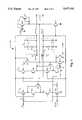
- FIG. 2is a detailed schematic diagram of the current source loop filter in FIG. 1.
- FIG. 1illustrates a block diagram of a phase-locked loop 10 employing a current source loop filter practiced in accordance with the principles of the present invention.
- the phase-locked loop 10comprises a phase comparator 12, loop filter 18, VCO 20, and prescaler 16.
- the phase comparator 12has differential inputs coupled to reference frequency generator 14 and prescaler 16, and has UP/DOWN output signals coupled to the input of a loop filter 18.
- the loop filter 18has PBIAS and NBIAS voltage outputs coupled to the input of voltage controlled oscillator 20.
- the differential output from the voltage controlled oscillator 20is coupled back through the prescaler 16 which divides it down and presents it to the phase comparator for comparison with the output from the reference frequency generator 14.
- phase comparator 12asserts the UP signal when the output of the voltage controlled oscillator 20 is lagging the frequency of the reference generator 14 and likewise asserts the DOWN signal when the frequency is leading the reference generator 14.
- prescalerdivides the frequency of the voltage controlled oscillator 20 by a divisor equal to the desired multiple frequency of the reference generator 14.
- FIG. 2depicts a detailed schematic diagram of the loop filter 18.
- P-channel MOSFET devicesare prefixed by MP while N-channel devices are prefixed by MN.
- Transistors MP1, MP2, MN2, and MN1are serially cascaded between the two power supply rails V DD and ground (V ss ).
- the UP signal from the phase comparator 12is coupled to the gate of MN3 and through an inverter 21 to the gate of transistor MP1.
- the Down signal from the phase comparator 12is coupled to the gate of MN1 and through an inverter 23 to the gate of transistor MP3.
- Transistor MP5has its source and drain coupled in parallel with that of transistor MP2.
- Transistors MP3, MP4, MN4, and MN3are serially cascaded between the two power supply rails V DD and ground.
- the gates of transistors MP2, MP4, and MP8are coupled to the PBIAS node, described in more detail hereinbelow.
- the gates of transistors MN2, MN4, and MN8are coupled to the NBIAS node, described in more detail hereinbelow.
- Transistor MN5has its source and drain coupled in parallel with that of transistor MN4.
- Transistors MN6 and MN7are coupled in parallel with their sources tied to the ground power supply rail and their drains coupled to the gate of transistor MN5 and to the drain of transistor MP8.
- Transistor MN6has its gate coupled to current source 25 while transistor MN7 is coupled in saturation with its gate coupled to its drain.
- Transistor MP8has its source coupled to the V DD power supply rail.
- Transistor MP6 and MP7are coupled in parallel with their sources tied to the V DD power supply rail and their; drains coupled to the gate of transistor MP5 and to the drain of MN8, Transistor MP6 has its gate coupled to current source 27 while transistor MP7 is coupled in saturation with its gate coupled to its drain. Transistor MN8 has its source coupled to the ground power supply rail.
- the PBIAS nodeis coupled through resistor R1 to the P-PUMP node formed by the junction of the drains of transistors MP4, MN4, and MNS.
- the PBIAS nodeis also coupled to the V DD power supply rail through the serial combination of resistor R2 and capacitor C2 in parallel with capacitor C1.
- the combination of R1, R2, C1, and C2forms a low pass filter 22 which integrates the current produced at the P-PUMP node to form a voltage at the PBIAS node.
- the NBIAS nodeis coupled through resistor R3 to the N-PUMP node formed by the junction of the drains of transistors MP2, MN2, and MPS.
- the NBIAS nodeis also coupled to the ground power supply rail through the serial combination of resistor R4 and capacitor C4 in parallel with capacitor C3.
- the combination of R3, R4, C3, and C4forms a low pass filter 24 which integrates the current produced at the N-PUMP node to form a voltage at the node NBIAS.
- Transistor MN1 and MP3are turned off terminating the current into the P-PUMP node for V DD .
- Transistor MN3is turned on pulling the sources of MN4 and MN5 and the P-PUMP node near the ground power: supply rail.
- Transistor MP1is turned on pulling the sources of transistors MP2 and MP5 near the V DD power supply rail and supplies current to the N-PUMP node, thus increasing the voltage across the NBIAS node which in turn commands the VCO 20 to raise its frequency.
- Transistor MN1is turned on pulling the source of transistor MN2 near the ground power supply rail and transistor MP1 is turned off severing the current into the N-PUMP node. As the voltage falls on the NBIAS node, transistor MN2 conducts less, draining less current from the N-PUMP node.
- Transistor MP3is turned on pulling the source of MP4 near the V DD power supply rail.
- the gate of MP4which is coupled through R1 to its drain, is initially at a voltage less than its source voltage, thus transistor MP4 conducts current from V DD into the P-PUMP node.
- the low pass filter 22integrates the current from the P-PUMP node to form a voltage on the PBIAS node.
- the gate-source voltage of transistor MP4approaches zero, forcing it to conduct less current into the P-PUMP node.
- the gate-source voltage of transistor MN2approaches zero, forcing it to shunt less current from the N-PUMP node.
- the PBIAS and NBIAS nodesthrottle back the current into the P-PUMP node and out of the N-PUMP node as the voltage on PBIAS approaches the V DD power supply rail and the voltage approaches the ground power supply rail on NBIAS.
- This throttlingis a form of automatic gain control to prevent MP4 and MN2 from going into saturation thus preventing the PBIAS node from reaching V DD and the NBIAS node from reaching ground which would stop the VCO 20.
- the second aspect of automatic gain control in the present inventioncompensates for the drain to source voltage (V DS )across transistors MP2 and MN2.
- V DS across transistor MP2approaches zero when the voltage across the NBIAS node approaches V DD . Consequently, the mount of current which can be conducted through MP2 is limited.
- transistor MP5is disposed in parallel with MP2.
- Transistor MP5is normally biased off unless the voltage across NBIAS rises to a level high enough to trigger conduction. More specifically, transistors MP6 and MP7 are coupled between V DD and the gate of MP5.
- Transistor MN8is coupled between the gate of MP5 and ground.
- Transistor MP7is coupled in a saturated mode (gate to drain) while transistor MP6 is sufficiently biased on by current source 27 to pull the gate of MP5 towards V DD so that transistor MP5 is turned off.
- transistor MN8conducts pulling the gate of MP5 to the ground power supply rail, thus turning on transistor MP5 and shunting it in parallel with transistor MP2.
- transistor MP5augments the amount of current flowing into the N-PUMP node. It will be understood by those skilled in the art that more than one transistor may be used for transistor MP5 to obtain the necessary current flow into the N-PUMP node as V DS approaches zero.
- the P-PUMP nodeis compensated in a like fashion.
- transistor MN5is disposed in parallel With transistor MN4.
- Transistor MN5is normally biased off unless the voltage across the PBIAS node falls low enough to trigger conduction.
- transistors MN6 and MN7are coupled between ground and the gate of MN5.
- Transistor MP8is coupled between the gate of MN5 and V DD .
- Transistor MN7is coupled in a saturated mode (gate to drain) while transistor MN6 is sufficiently biased on by current source 25 to pull the gate of MN5 towards ground so that transistor MN5 is turned off.
- transistor MP8conducts pulling the gate of MN5 to the V DD power supply rail, thus shunting MN5 in parallel with transistor MN4. In this manner, transistor MN5 augments the mount current supplied to the P-PUMP node. It will be understood by those skilled in the art that more than one transistor may be used for transistor MN5 to obtain the necessary current flow into the P-PUMP node.
Landscapes
- Stabilization Of Oscillater, Synchronisation, Frequency Synthesizers (AREA)
Abstract
Description
Claims (8)
Priority Applications (1)
| Application Number | Priority Date | Filing Date | Title |
|---|---|---|---|
| US08/327,070US5477193A (en) | 1994-10-21 | 1994-10-21 | Current source loop filter with automatic gain control |
Applications Claiming Priority (1)
| Application Number | Priority Date | Filing Date | Title |
|---|---|---|---|
| US08/327,070US5477193A (en) | 1994-10-21 | 1994-10-21 | Current source loop filter with automatic gain control |
Publications (1)
| Publication Number | Publication Date |
|---|---|
| US5477193Atrue US5477193A (en) | 1995-12-19 |
Family
ID=23275013
Family Applications (1)
| Application Number | Title | Priority Date | Filing Date |
|---|---|---|---|
| US08/327,070Expired - LifetimeUS5477193A (en) | 1994-10-21 | 1994-10-21 | Current source loop filter with automatic gain control |
Country Status (1)
| Country | Link |
|---|---|
| US (1) | US5477193A (en) |
Cited By (14)
| Publication number | Priority date | Publication date | Assignee | Title |
|---|---|---|---|---|
| US5703511A (en)* | 1996-06-19 | 1997-12-30 | Fujitsu Limited | Charge pump circuit, PLL circuit with charge pump circuit, and semiconductor integrated circuit with charge pump circuit |
| US5809095A (en)* | 1995-02-10 | 1998-09-15 | Kabushiki Kaisha Toshiba | Synchronous signal output circuit |
| GB2336482A (en)* | 1998-04-14 | 1999-10-20 | Motorola Israel Ltd | Phase lock loop with differential charge pump |
| US6118316A (en)* | 1996-05-08 | 2000-09-12 | Fujitsu Limited | Semiconductor integrated circuit including plurality of phase-locked loops |
| US6222402B1 (en)* | 1998-09-04 | 2001-04-24 | International Business Machines Corporation | Differential charge-pump with improved linearity |
| US6385265B1 (en)* | 1998-08-04 | 2002-05-07 | Cypress Semiconductor Corp. | Differential charge pump |
| US6437615B1 (en)* | 2001-09-13 | 2002-08-20 | Lsi Logic Corporation | Loop filter and method for generating a control signal in phase-locked loop circuits |
| US6529082B1 (en)* | 2001-10-11 | 2003-03-04 | International Business Machines Corporation | Dual mode charge pump |
| DE10128384B4 (en)* | 2000-06-09 | 2004-02-05 | Samsung Electronics Co., Ltd., Suwon | Charge pump circuit |
| US20040080359A1 (en)* | 2002-10-25 | 2004-04-29 | Exar Corporation | Loop filter capacitor multiplication in a charge pump circuit |
| US20040085106A1 (en)* | 2002-08-26 | 2004-05-06 | Integrant Technologies Inc. | Charge pump circuit for compensating mismatch of output currents |
| US20040169536A1 (en)* | 2000-12-13 | 2004-09-02 | Intel Corporation | Phase indication apparatus |
| US6809600B2 (en) | 2001-09-17 | 2004-10-26 | Rambus Inc. | Dual loop phase lock loops using dual voltage supply regulators |
| US6928128B1 (en) | 1999-05-03 | 2005-08-09 | Rambus Inc. | Clock alignment circuit having a self regulating voltage supply |
Citations (11)
| Publication number | Priority date | Publication date | Assignee | Title |
|---|---|---|---|---|
| US3594649A (en)* | 1969-02-14 | 1971-07-20 | Minnesota Mining & Mfg | Voltage-controlled oscillator |
| US4498020A (en)* | 1981-10-19 | 1985-02-05 | Texas Instruments Incorporated | Current to frequency converter |
| US4692717A (en)* | 1986-03-14 | 1987-09-08 | Western Digital Corporation | Voltage controlled oscillator with high speed current switching |
| US4812784A (en)* | 1987-11-19 | 1989-03-14 | International Business Machines Corporation | Temperature stable voltage controlled oscillator with super linear wide frequency range |
| US4922139A (en)* | 1988-03-30 | 1990-05-01 | Deutsche Itt Industries Gmbh | Filter circuit for generating a VCO control voltage responsive to the output signals from a frequency/phase discriminator |
| US4959618A (en)* | 1989-02-16 | 1990-09-25 | Vtc Incorporated | Differential charge pump for a phase locked loop |
| US4987387A (en)* | 1989-09-08 | 1991-01-22 | Delco Electronics Corporation | Phase locked loop circuit with digital control |
| US5300898A (en)* | 1992-07-29 | 1994-04-05 | Ncr Corporation | High speed current/voltage controlled ring oscillator circuit |
| US5341113A (en)* | 1992-07-02 | 1994-08-23 | Motorola, Inc. | Voltage controlled oscillator having a 50% duty cycle |
| US5384502A (en)* | 1993-06-24 | 1995-01-24 | Intel Corporation | Phase locked loop circuitry with split loop filter |
| US5422603A (en)* | 1994-06-02 | 1995-06-06 | International Business Machines Corporation | CMOS frequency synthesizer |
- 1994
- 1994-10-21USUS08/327,070patent/US5477193A/ennot_activeExpired - Lifetime
Patent Citations (11)
| Publication number | Priority date | Publication date | Assignee | Title |
|---|---|---|---|---|
| US3594649A (en)* | 1969-02-14 | 1971-07-20 | Minnesota Mining & Mfg | Voltage-controlled oscillator |
| US4498020A (en)* | 1981-10-19 | 1985-02-05 | Texas Instruments Incorporated | Current to frequency converter |
| US4692717A (en)* | 1986-03-14 | 1987-09-08 | Western Digital Corporation | Voltage controlled oscillator with high speed current switching |
| US4812784A (en)* | 1987-11-19 | 1989-03-14 | International Business Machines Corporation | Temperature stable voltage controlled oscillator with super linear wide frequency range |
| US4922139A (en)* | 1988-03-30 | 1990-05-01 | Deutsche Itt Industries Gmbh | Filter circuit for generating a VCO control voltage responsive to the output signals from a frequency/phase discriminator |
| US4959618A (en)* | 1989-02-16 | 1990-09-25 | Vtc Incorporated | Differential charge pump for a phase locked loop |
| US4987387A (en)* | 1989-09-08 | 1991-01-22 | Delco Electronics Corporation | Phase locked loop circuit with digital control |
| US5341113A (en)* | 1992-07-02 | 1994-08-23 | Motorola, Inc. | Voltage controlled oscillator having a 50% duty cycle |
| US5300898A (en)* | 1992-07-29 | 1994-04-05 | Ncr Corporation | High speed current/voltage controlled ring oscillator circuit |
| US5384502A (en)* | 1993-06-24 | 1995-01-24 | Intel Corporation | Phase locked loop circuitry with split loop filter |
| US5422603A (en)* | 1994-06-02 | 1995-06-06 | International Business Machines Corporation | CMOS frequency synthesizer |
Cited By (17)
| Publication number | Priority date | Publication date | Assignee | Title |
|---|---|---|---|---|
| US5809095A (en)* | 1995-02-10 | 1998-09-15 | Kabushiki Kaisha Toshiba | Synchronous signal output circuit |
| US6118316A (en)* | 1996-05-08 | 2000-09-12 | Fujitsu Limited | Semiconductor integrated circuit including plurality of phase-locked loops |
| US5703511A (en)* | 1996-06-19 | 1997-12-30 | Fujitsu Limited | Charge pump circuit, PLL circuit with charge pump circuit, and semiconductor integrated circuit with charge pump circuit |
| GB2336482A (en)* | 1998-04-14 | 1999-10-20 | Motorola Israel Ltd | Phase lock loop with differential charge pump |
| GB2336482B (en)* | 1998-04-14 | 2000-06-07 | Motorola Israel Ltd | Phase lock loop and differential charge pump |
| US6385265B1 (en)* | 1998-08-04 | 2002-05-07 | Cypress Semiconductor Corp. | Differential charge pump |
| US6222402B1 (en)* | 1998-09-04 | 2001-04-24 | International Business Machines Corporation | Differential charge-pump with improved linearity |
| US6928128B1 (en) | 1999-05-03 | 2005-08-09 | Rambus Inc. | Clock alignment circuit having a self regulating voltage supply |
| DE10128384B4 (en)* | 2000-06-09 | 2004-02-05 | Samsung Electronics Co., Ltd., Suwon | Charge pump circuit |
| US20040169536A1 (en)* | 2000-12-13 | 2004-09-02 | Intel Corporation | Phase indication apparatus |
| US6812757B2 (en)* | 2000-12-13 | 2004-11-02 | Intel Corporation | Phase lock loop apparatus |
| US6437615B1 (en)* | 2001-09-13 | 2002-08-20 | Lsi Logic Corporation | Loop filter and method for generating a control signal in phase-locked loop circuits |
| US6809600B2 (en) | 2001-09-17 | 2004-10-26 | Rambus Inc. | Dual loop phase lock loops using dual voltage supply regulators |
| US6529082B1 (en)* | 2001-10-11 | 2003-03-04 | International Business Machines Corporation | Dual mode charge pump |
| US20040085106A1 (en)* | 2002-08-26 | 2004-05-06 | Integrant Technologies Inc. | Charge pump circuit for compensating mismatch of output currents |
| US6744292B2 (en)* | 2002-10-25 | 2004-06-01 | Exar Corporation | Loop filter capacitor multiplication in a charge pump circuit |
| US20040080359A1 (en)* | 2002-10-25 | 2004-04-29 | Exar Corporation | Loop filter capacitor multiplication in a charge pump circuit |
Similar Documents
| Publication | Publication Date | Title |
|---|---|---|
| US5477193A (en) | Current source loop filter with automatic gain control | |
| US5563553A (en) | Method and apparatus for a controlled oscillation that may be used in a phase locked loop | |
| US5175512A (en) | High speed, power supply independent CMOS voltage controlled ring oscillator with level shifting circuit | |
| US6809600B2 (en) | Dual loop phase lock loops using dual voltage supply regulators | |
| JP3356136B2 (en) | PLL circuit | |
| US6960949B2 (en) | Charge pump circuit and PLL circuit using same | |
| US5600284A (en) | High performance voltage controlled oscillator | |
| US5298870A (en) | Voltage controlled ring oscillator having differential amplifier stages | |
| EP0583586B1 (en) | Charge pump in a phase lock loop | |
| US6316977B1 (en) | Low charge-injection charge pump | |
| US8164366B2 (en) | Locked loops, bias generators, charge pumps and methods for generating control voltages | |
| US20080061895A1 (en) | Improved current controlled oscillation device and method having wide frequency range | |
| US6107889A (en) | Phase locked loop charge pump circuit | |
| US11742863B2 (en) | Phase-locked loop circuit | |
| US5081428A (en) | Voltage controlled oscillator having 50% duty cycle clock | |
| US5760657A (en) | Method and apparatus employing a process dependent impedance that compensates for manufacturing variations in a voltage controlled oscillator | |
| US6255873B1 (en) | Setting the common mode level of a differential charge pump output | |
| US5714912A (en) | VCO supply voltage regulator | |
| US5880579A (en) | VCO supply voltage regulator for PLL | |
| US6853254B2 (en) | Anti-deadlock circuit and method for phase-locked loops | |
| US5081429A (en) | Voltage controlled oscillator with controlled load | |
| US5818287A (en) | Gate-switching charge-pump implemented inside a phase locked loop | |
| EP0545517B1 (en) | Gate multiplexed low noise charge pump | |
| US5434545A (en) | Fully differential voltage controlled oscillator | |
| KR20000018820A (en) | Phase locked loop circuit for reducing lock-in-time |
Legal Events
| Date | Code | Title | Description |
|---|---|---|---|
| AS | Assignment | Owner name:CYRIX CORPORATION, TEXAS Free format text:ASSIGNMENT OF ASSIGNORS INTEREST;ASSIGNOR:BURCHFIELD, MARK E.;REEL/FRAME:007220/0389 Effective date:19941020 | |
| AS | Assignment | Owner name:IBM CREDIT CORPORATION, CONNECTICUT Free format text:SECURITY INTEREST;ASSIGNOR:CYRIX, CORPORATION;REEL/FRAME:007757/0320 Effective date:19950619 | |
| STCF | Information on status: patent grant | Free format text:PATENTED CASE | |
| AS | Assignment | Owner name:NATIONAL SEMICONDUCTOR CORP, CALIFORNIA Free format text:ASSIGNMENT OF ASSIGNORS INTEREST;ASSIGNOR:CYRIX CORPORATION;REEL/FRAME:009089/0068 Effective date:19980309 | |
| FPAY | Fee payment | Year of fee payment:4 | |
| FEPP | Fee payment procedure | Free format text:PAYOR NUMBER ASSIGNED (ORIGINAL EVENT CODE: ASPN); ENTITY STATUS OF PATENT OWNER: LARGE ENTITY | |
| FPAY | Fee payment | Year of fee payment:8 | |
| AS | Assignment | Owner name:ADVANCED MICRO DEVICES, INC., CALIFORNIA Free format text:ASSIGNMENT OF ASSIGNORS INTEREST;ASSIGNOR:NATIONAL SEMICONDUCTOR CORPORATION BY JOHN M. CLARK III, SR. V.P. AND SECRETARY;REEL/FRAME:014692/0568 Effective date:20030821 Owner name:ADVANCED MICRO DEVICES, INC., CALIFORNIA Free format text:ASSIGNMENT OF ASSIGNORS INTEREST;ASSIGNOR:NATIONAL SEMICONDUCTOR CORPORATION BY JOHN M. CLARK III, SR. V.P. AND SECRETARY;REEL/FRAME:014693/0765 Effective date:20030821 | |
| FEPP | Fee payment procedure | Free format text:PAYER NUMBER DE-ASSIGNED (ORIGINAL EVENT CODE: RMPN); ENTITY STATUS OF PATENT OWNER: LARGE ENTITY Free format text:PAYOR NUMBER ASSIGNED (ORIGINAL EVENT CODE: ASPN); ENTITY STATUS OF PATENT OWNER: LARGE ENTITY | |
| FPAY | Fee payment | Year of fee payment:12 |