US5475318A - Microprobe - Google Patents
MicroprobeDownload PDFInfo
- Publication number
- US5475318A US5475318AUS08/145,403US14540393AUS5475318AUS 5475318 AUS5475318 AUS 5475318AUS 14540393 AUS14540393 AUS 14540393AUS 5475318 AUS5475318 AUS 5475318A
- Authority
- US
- United States
- Prior art keywords
- cantilever
- layer
- contact
- contact zone
- substrate
- Prior art date
- Legal status (The legal status is an assumption and is not a legal conclusion. Google has not performed a legal analysis and makes no representation as to the accuracy of the status listed.)
- Expired - Fee Related
Links
- 239000000523sampleSubstances0.000claimsabstractdescription97
- VYPSYNLAJGMNEJ-UHFFFAOYSA-NSilicium dioxideChemical compoundO=[Si]=OVYPSYNLAJGMNEJ-UHFFFAOYSA-N0.000claimsabstractdescription43
- 229910052710siliconInorganic materials0.000claimsabstractdescription33
- 239000010703siliconSubstances0.000claimsabstractdescription33
- 239000000463materialSubstances0.000claimsabstractdescription29
- 238000010438heat treatmentMethods0.000claimsabstractdescription22
- 229910052782aluminiumInorganic materials0.000claimsabstractdescription15
- XAGFODPZIPBFFR-UHFFFAOYSA-NaluminiumChemical compound[Al]XAGFODPZIPBFFR-UHFFFAOYSA-N0.000claimsabstractdescription13
- 229910021420polycrystalline siliconInorganic materials0.000claimsabstractdescription11
- 229920005591polysiliconPolymers0.000claimsabstractdescription11
- 229910052751metalInorganic materials0.000claimsabstractdescription10
- 239000002184metalSubstances0.000claimsabstractdescription10
- 239000004020conductorSubstances0.000claimsabstractdescription4
- 229910052814silicon oxideInorganic materials0.000claimsabstractdescription3
- 239000000758substrateSubstances0.000claimsdescription23
- WFKWXMTUELFFGS-UHFFFAOYSA-NtungstenChemical compound[W]WFKWXMTUELFFGS-UHFFFAOYSA-N0.000claimsdescription5
- 229910052721tungstenInorganic materials0.000claimsdescription5
- 239000010937tungstenSubstances0.000claimsdescription5
- 238000005452bendingMethods0.000claimsdescription4
- HBMJWWWQQXIZIP-UHFFFAOYSA-Nsilicon carbideChemical compound[Si+]#[C-]HBMJWWWQQXIZIP-UHFFFAOYSA-N0.000claimsdescription4
- 229910010271silicon carbideInorganic materials0.000claimsdescription4
- 229910003460diamondInorganic materials0.000claimsdescription3
- 239000010432diamondSubstances0.000claimsdescription3
- 229910052763palladiumInorganic materials0.000claimsdescription3
- 239000007769metal materialSubstances0.000claims3
- KDLHZDBZIXYQEI-UHFFFAOYSA-NPalladiumChemical compound[Pd]KDLHZDBZIXYQEI-UHFFFAOYSA-N0.000claims2
- 230000005611electricityEffects0.000claims1
- 238000011835investigationMethods0.000abstractdescription6
- 239000010410layerSubstances0.000description64
- XUIMIQQOPSSXEZ-UHFFFAOYSA-NSiliconChemical compound[Si]XUIMIQQOPSSXEZ-UHFFFAOYSA-N0.000description28
- 238000000034methodMethods0.000description24
- 235000012431wafersNutrition0.000description22
- 229910052681coesiteInorganic materials0.000description20
- 229910052906cristobaliteInorganic materials0.000description20
- 239000000377silicon dioxideSubstances0.000description20
- 229910052682stishoviteInorganic materials0.000description20
- 229910052905tridymiteInorganic materials0.000description20
- 238000005530etchingMethods0.000description12
- 230000008569processEffects0.000description12
- 238000012545processingMethods0.000description7
- 238000004630atomic force microscopyMethods0.000description5
- 239000007788liquidSubstances0.000description5
- 230000003647oxidationEffects0.000description5
- 238000007254oxidation reactionMethods0.000description5
- 239000010408filmSubstances0.000description4
- 238000004519manufacturing processMethods0.000description4
- 238000012360testing methodMethods0.000description4
- 238000005259measurementMethods0.000description3
- 239000007858starting materialSubstances0.000description3
- ZOXJGFHDIHLPTG-UHFFFAOYSA-NBoronChemical compound[B]ZOXJGFHDIHLPTG-UHFFFAOYSA-N0.000description2
- XLOMVQKBTHCTTD-UHFFFAOYSA-NZinc monoxideChemical compound[Zn]=OXLOMVQKBTHCTTD-UHFFFAOYSA-N0.000description2
- QVGXLLKOCUKJST-UHFFFAOYSA-Natomic oxygenChemical compound[O]QVGXLLKOCUKJST-UHFFFAOYSA-N0.000description2
- 230000008901benefitEffects0.000description2
- 230000015572biosynthetic processEffects0.000description2
- 229910052796boronInorganic materials0.000description2
- 238000012512characterization methodMethods0.000description2
- 238000005229chemical vapour depositionMethods0.000description2
- 238000000151depositionMethods0.000description2
- 238000005516engineering processMethods0.000description2
- 238000002513implantationMethods0.000description2
- 238000004377microelectronicMethods0.000description2
- 229910021421monocrystalline siliconInorganic materials0.000description2
- 239000001301oxygenSubstances0.000description2
- 229910052760oxygenInorganic materials0.000description2
- 229920002120photoresistant polymerPolymers0.000description2
- 150000003376siliconChemical class0.000description2
- 239000007787solidSubstances0.000description2
- 230000007480spreadingEffects0.000description2
- 238000003892spreadingMethods0.000description2
- 238000010561standard procedureMethods0.000description2
- RZVAJINKPMORJF-UHFFFAOYSA-NAcetaminophenChemical compoundCC(=O)NC1=CC=C(O)C=C1RZVAJINKPMORJF-UHFFFAOYSA-N0.000description1
- GRYLNZFGIOXLOG-UHFFFAOYSA-NNitric acidChemical compoundO[N+]([O-])=OGRYLNZFGIOXLOG-UHFFFAOYSA-N0.000description1
- 238000001015X-ray lithographyMethods0.000description1
- 239000003082abrasive agentSubstances0.000description1
- 230000009471actionEffects0.000description1
- 238000002048anodisation reactionMethods0.000description1
- 238000003491arrayMethods0.000description1
- 238000010276constructionMethods0.000description1
- 238000011109contaminationMethods0.000description1
- 230000008021depositionEffects0.000description1
- 239000003989dielectric materialSubstances0.000description1
- 238000001312dry etchingMethods0.000description1
- 239000002355dual-layerSubstances0.000description1
- 238000000609electron-beam lithographyMethods0.000description1
- 239000007789gasSubstances0.000description1
- PCHJSUWPFVWCPO-UHFFFAOYSA-NgoldChemical compound[Au]PCHJSUWPFVWCPO-UHFFFAOYSA-N0.000description1
- 229910052737goldInorganic materials0.000description1
- 239000010931goldSubstances0.000description1
- 230000007246mechanismEffects0.000description1
- 230000008018meltingEffects0.000description1
- 238000002844meltingMethods0.000description1
- 239000012528membraneSubstances0.000description1
- 238000005459micromachiningMethods0.000description1
- 239000000203mixtureSubstances0.000description1
- 229910017604nitric acidInorganic materials0.000description1
- 230000001590oxidative effectEffects0.000description1
- 230000002093peripheral effectEffects0.000description1
- 238000000206photolithographyMethods0.000description1
- 238000001953recrystallisationMethods0.000description1
- 239000004065semiconductorSubstances0.000description1
- 239000010409thin filmSubstances0.000description1
- 230000005641tunnelingEffects0.000description1
- 239000011787zinc oxideSubstances0.000description1
Images


Classifications
- G—PHYSICS
- G01—MEASURING; TESTING
- G01R—MEASURING ELECTRIC VARIABLES; MEASURING MAGNETIC VARIABLES
- G01R1/00—Details of instruments or arrangements of the types included in groups G01R5/00 - G01R13/00 and G01R31/00
- G01R1/02—General constructional details
- G01R1/06—Measuring leads; Measuring probes
- G01R1/067—Measuring probes
- G01R1/06711—Probe needles; Cantilever beams; "Bump" contacts; Replaceable probe pins
- G01R1/06716—Elastic
- G01R1/06727—Cantilever beams
- G—PHYSICS
- G01—MEASURING; TESTING
- G01R—MEASURING ELECTRIC VARIABLES; MEASURING MAGNETIC VARIABLES
- G01R1/00—Details of instruments or arrangements of the types included in groups G01R5/00 - G01R13/00 and G01R31/00
- G01R1/02—General constructional details
- G01R1/06—Measuring leads; Measuring probes
- G01R1/067—Measuring probes
- G01R1/06711—Probe needles; Cantilever beams; "Bump" contacts; Replaceable probe pins
- G—PHYSICS
- G01—MEASURING; TESTING
- G01R—MEASURING ELECTRIC VARIABLES; MEASURING MAGNETIC VARIABLES
- G01R1/00—Details of instruments or arrangements of the types included in groups G01R5/00 - G01R13/00 and G01R31/00
- G01R1/02—General constructional details
- G01R1/06—Measuring leads; Measuring probes
- G01R1/067—Measuring probes
- G01R1/073—Multiple probes
- G01R1/07307—Multiple probes with individual probe elements, e.g. needles, cantilever beams or bump contacts, fixed in relation to each other, e.g. bed of nails fixture or probe card
- G01R1/07342—Multiple probes with individual probe elements, e.g. needles, cantilever beams or bump contacts, fixed in relation to each other, e.g. bed of nails fixture or probe card the body of the probe being at an angle other than perpendicular to test object, e.g. probe card
- G—PHYSICS
- G01—MEASURING; TESTING
- G01R—MEASURING ELECTRIC VARIABLES; MEASURING MAGNETIC VARIABLES
- G01R1/00—Details of instruments or arrangements of the types included in groups G01R5/00 - G01R13/00 and G01R31/00
- G01R1/02—General constructional details
- G01R1/06—Measuring leads; Measuring probes
- G01R1/067—Measuring probes
- G01R1/073—Multiple probes
- G01R1/07392—Multiple probes manipulating each probe element or tip individually
- H—ELECTRICITY
- H01—ELECTRIC ELEMENTS
- H01H—ELECTRIC SWITCHES; RELAYS; SELECTORS; EMERGENCY PROTECTIVE DEVICES
- H01H1/00—Contacts
- H01H1/0036—Switches making use of microelectromechanical systems [MEMS]
- H—ELECTRICITY
- H01—ELECTRIC ELEMENTS
- H01H—ELECTRIC SWITCHES; RELAYS; SELECTORS; EMERGENCY PROTECTIVE DEVICES
- H01H61/00—Electrothermal relays
- H01H2061/006—Micromechanical thermal relay
- H—ELECTRICITY
- H01—ELECTRIC ELEMENTS
- H01H—ELECTRIC SWITCHES; RELAYS; SELECTORS; EMERGENCY PROTECTIVE DEVICES
- H01H61/00—Electrothermal relays
- H01H61/02—Electrothermal relays wherein the thermally-sensitive member is heated indirectly, e.g. resistively, inductively
- Y—GENERAL TAGGING OF NEW TECHNOLOGICAL DEVELOPMENTS; GENERAL TAGGING OF CROSS-SECTIONAL TECHNOLOGIES SPANNING OVER SEVERAL SECTIONS OF THE IPC; TECHNICAL SUBJECTS COVERED BY FORMER USPC CROSS-REFERENCE ART COLLECTIONS [XRACs] AND DIGESTS
- Y10—TECHNICAL SUBJECTS COVERED BY FORMER USPC
- Y10S—TECHNICAL SUBJECTS COVERED BY FORMER USPC CROSS-REFERENCE ART COLLECTIONS [XRACs] AND DIGESTS
- Y10S977/00—Nanotechnology
- Y10S977/84—Manufacture, treatment, or detection of nanostructure
- Y10S977/849—Manufacture, treatment, or detection of nanostructure with scanning probe
- Y10S977/86—Scanning probe structure
- Y10S977/872—Positioner
- Y—GENERAL TAGGING OF NEW TECHNOLOGICAL DEVELOPMENTS; GENERAL TAGGING OF CROSS-SECTIONAL TECHNOLOGIES SPANNING OVER SEVERAL SECTIONS OF THE IPC; TECHNICAL SUBJECTS COVERED BY FORMER USPC CROSS-REFERENCE ART COLLECTIONS [XRACs] AND DIGESTS
- Y10—TECHNICAL SUBJECTS COVERED BY FORMER USPC
- Y10S—TECHNICAL SUBJECTS COVERED BY FORMER USPC CROSS-REFERENCE ART COLLECTIONS [XRACs] AND DIGESTS
- Y10S977/00—Nanotechnology
- Y10S977/84—Manufacture, treatment, or detection of nanostructure
- Y10S977/849—Manufacture, treatment, or detection of nanostructure with scanning probe
- Y10S977/86—Scanning probe structure
- Y10S977/873—Tip holder
Definitions
- the present inventionis in the field of microelectromechanical systems (MEMS). More particularly, the present invention relates to a microcantilever. In one of its aspects, the present invention is directed to a microprobe which incorporates the microcantilever and which is used for high resolution material characterization. In another of its aspects, the present invention is directed to a conformable, high-pin count, programmable wafer probe (called a CHIPP probe card) which incorporates an array of the microcantilevers for device characterization.
- MEMSmicroelectromechanical systems
- J. Brugger et aldisclose a method for producing monocrystalline silicon cantilevers with integrated silicon tips. These microcantilevers are produced by micro-machining techniques. They are described as being useful as microprobes to measure friction during atomic force microscopy (AFM). This article also describes the fabrication of an array of such microprobes which enables multiple parallel or serial surface profiling to be achieved.
- AFMatomic force microscopy
- T. R. Albrecht et alin J. Vac. Sci. Tech. A, 8 (4), p. 3386 (1990), also disclose a method of fabricating sharp Si tips on microcantilevers for use in atomic force microscopy.
- Park Scientific Instruments, Inc.of Sunnyvale, Calif., sells Si cantilevers with Si tips for use in atomic force microscopy
- the Nanoprobe company of Germanyalso sells cantilevers with Si tips for atomic force microscopy.
- Only the Albrech et al. deviceincludes an actuator integrated with the cantilever, although the mechanism for actuating the cantilevers is not described.
- T. Albrecht et aldisclose a process for microfabricating arrays of scanning tunnelling microscopes (STM) on silicon wafers.
- STMscanning tunnelling microscopes
- Each scanning tunnelling microscopecomprises a tunneling tip projecting from a piezoelectric actuator.
- the actuatoris in the form of a bimorph cantilever constructed from alternating layers of multiple metallic electrodes, dielectric films, and piezoelectric zinc oxide films.
- microprobecomprising a microcantilever having a probe tip projecting from the microcantilever, wherein the microcantilever is of bimorph construction with an integrated heating element.
- a microprobecomprising a bimorph actuated microcantilever having a probe tip which projects from the microcantilever.
- the probe tipmay be atomically sharp or less sharp. Upon heating of the microcantilever, the probe tip comes into contact with a material to be investigated.
- a microprobecomprising a base, a microcantilever extending in a plane from the base, and a probe contact projecting from the microcantilever out of the plane.
- the probe contactis a sharp tip, while in another embodiment, the probe contact is a planar tip.
- the microcantileveris a bimorph structure comprising first and second layers made from materials having different coefficients of thermal expansion, and an integrated heating element as an actuator for supplying heat to the microcantilever.
- the probe tipis made from silicon and comes to a radius that can be controlled to atomic sharpness (radius of ⁇ 1 nm.)
- the bimorph microcantileveris made from a metal, such as aluminum, and silicon oxide as the materials of the two layers.
- the heating elementcomprises a line or ribbon of a conductive material, such as polysilicon which is in contact with one of two layers, and supplies heat, thereby causing the probe tip to traverse an arc and bring it into contact with a material under investigation.
- the microcantileveris a piezoelectric (electrostrictive) thin film element which is actuated (i.e., caused to traverse an arc) by impressing a voltage across the piezoelectric film.
- the inventive microprobeis a monolithic structure, i.e., is fashioned from a single piece of semiconductor using the techniques of silicon chip processing.
- an array of the individually addressable microprobes of the kind described aboveare fashioned out of a silicon wafer and are connected by appropriate leads to the outside world so as to form a wafer probe card.
- This arraymay comprise as many as 15,000 individual microprobes per cm 2 of the kind described above.
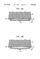
- FIG. 1is a perspective view illustrating a microprobe in accordance with the present invention.
- FIG. 2is a cross-sectional view of the inventive microprobe.
- FIGS. 3a-3fschematically illustrate a process for producing the inventive microprobe shown in FIGS. 1 and 2.
- FIG. 4illustrates another embodiment of the invention for probing resistivity of materials.
- FIG. 5illustrates a wafer probe card incorporating an array of the inventive microbes.
- FIGS. 6-7are cross-sectional views of one portion of the wafer probe card shown in FIG. 5.
- FIGS. 8a-8care views of another embodiment of the microprobe of the present invention.
- FIGS. 9a-9bare views of another embodiment of the inventive microprobe.
- FIGS. 10a-10bare views of another embodiment of the inventive microprobe.
- FIGS. 11a-11bare views of another embodiment of the inventive microprobe.
- FIGS. 12a-12bare views of yet another embodiment of the inventive microprobe.
- the basic microprobe structure 10 shown in FIG. 1comprises a single probe tip 12, a bimorph cantilever 14, and a heating element 16.
- the bimorph 14is a dual layer cantilever or beam which projects outwardly from a base area and is suspended over an air gap 18.
- the cantilevercan comprise a beam made from a piezoelectric material which is actuated by the passage of electric current.
- the cantilever 14is about 200-600 ⁇ m long and about 20-30 ⁇ m wide.
- the probe tip 12, which is made from silicon,is about 5 ⁇ m long. The sharpness of the point of the silicon tip 12 can be varied.
- the point of probe tip 12is very sharp (radius of less than 1 nm, typically about 0.5 nm), which enables it to break through surface oxides when functioning to probe material surface characteristics.
- the probe tipis a planar structure.
- the air gap 18is about 10 ⁇ m wide.
- the bimorph structure of cantilever 14comprises a layer of aluminum 106 that is about 1.5 ⁇ m thick and a layer 108 of SiO 2 that is about 1 ⁇ m micron thick.
- a ribbon of conductive polysilicon 110 about 0.5 ⁇ m thickconstitutes the heating element 16. Due to the differences in the coefficient of thermal expansion of Al and SiO 2 , the cantilever 14 illustrated in FIG. 1, which is 200 ⁇ m long and 20 ⁇ m wide, will traverse an arc corresponding to a vertical distance of about 10 ⁇ m when supplying 50 mW power to the heating element 16 thereby raising the bimorph temperature to 150° C. The same temperature can be obtained, and the same distance can be traversed by cantilever 14, with a heating power of only 150 ⁇ W in a vacuum of 10 -4 Torr. Thus, probing in vacuum is far more efficient than probing in air.
- cantilever 14is made longer. For example, a vertical distance of 50 ⁇ m can be traversed if the cantilever is 500 ⁇ m long. In all cases, the direction of travel of cantilever 14 is upward as shown in FIG. 1, i.e., away from air gap 18. However, it is possible to construct the microcantilever with the layers 106 and 108 reversed and with the probe tip 12 pointed downward. In that case, the direction of travel will be downward, referring to FIG. 1.
- FIG. 2a cross sectional view of the basic microprobe structure 10 of FIG. 1 is shown.
- This structurecomprises a silicon substrate 100 on which various layers have been deposited and etched away in selected locations to provide the microprobe structure shown in FIGS. 1 and 2. These layers include a layer 102 of SiO 2 that is about 0.4 ⁇ m thick, a layer 104 of Pd that is about 200 ⁇ thick, the layers 106 and 108 of Al and SiO 2 respectively which constitute the bimorph actuator, and the layer 110 of polysilicon which constitutes the integrated heating element of the bimorph actuator.
- a layer 112 of p ++ Siwhich has been doped with boron. It will be recognized that FIGS. 1 and 2 illustrate only one of an array of microprobes that can be formed in substrate 100 by standard silicon processing techniques.
- FIGS. 3a-3fillustrate a series of silicon processing steps which may be used to produce the basic microprobe structure 10 shown in FIGS. 1 and 2 as well as other similar microprobes in substrate 100. It should be understood that the series of silicon processing steps diagrammatically illustrated in FIGS. 3a-3f are illustrative only. A different series of steps may also be used to produce the final structure.
- the starting materialconsists of the single crystal silicon substrate 100, on top of which is a layer of SiO 2 102 buried beneath the surface, and which has been formed by oxygen implantation.
- the silicon on top of the SiO 2 layer 102is the layer 112 of boron doped p ++ Si, and on top of this is a layer 114 of epitaxially deposited silicon.
- the desired silicon probe tip 12 of FIG. 3fwill be formed from the epitaxially deposited silicon 114, using the SiO 2 mask 116 of FIG. 3b is placed on the epi Si at the location beneath which the probe tip 12 will be formed.
- the same structuremay be formed by oxygen implantation into silicon, melting and recrystallization of a polysilicon film on an oxidized wafer, wafer bonding, or by any other recognized method.
- the starting materials shown in FIG. 3aare subjected to either a one-step or a two-step etching process to remove most of the layer 114 of epi Si except under mask 116 and thereby begin the formation of probe tip 12.
- a two-step etching processis preferred since it results in a probe tip having a higher aspect ratio than a one-step etching process.
- the starting materialsare first subjected to a dry etching process using SiF x Cl y gas at an elevated temperature (e.g., 400°-600° C.), to remove some of the epi Si layer.
- an elevated temperaturee.g. 400°-600° C.
- the materialsare subjected to either anisotropic liquid etching using KOH, or else isotropic liquid etching using a combination of HF, HNO 3 , and CH 3 COOH, to begin the formation of probe tip 12.
- the liquid etchantattacks from the sides underneath mask 116 leaving a structure similar to that shown in FIG. 3b under oxide mask 116. If isotropic etching is used, the sides of probe tip 12 are rounded, while anisotropic etching will produce square sides on probe tip 12 for the case where the silicon wafer was oriented with the (100) crystal-lographic plane parallel to its surface.
- the oxide mask 116is next removed using HF. Thereafter, the projection 118 is sharpened into probe tip 12 using the oxidation techniques described in the publications of R. B. Marcus et al. For example, the projection 118 is subjected to oxidizing at temperatures in the range 850° C.-1,050° C. for periods of 2-5 hours. Thereafter, the oxide layers which have been produced are removed by standard techniques described in these publications. The resulting structure is shown in FIG. 3c. Alternatively, in cases where a tip with less curvature is desired, the radius can be increased by high-temperature oxidation ( ⁇ 1050° C.), anodization, or etching.
- the atomically sharp probe tip 12has been formed with layers 102 of SiO 2 and 112 of p ++ Si underneath probe tip 12. It is now necessary to form the cantilever 14 from which probe tip 12 will project. This is accomplished in a series of steps between FIG. 3c and FIG. 3d.
- the first stepis to deposit another oxide mask 120 on the surface of substrate 100 and on probe tip 12 using CVD (chemical vapor deposition) techniques. Thereafter, this oxide mask 120 is removed everywhere except from the probe tip 12. Thus, an oxide mask 120 is left on the probe tip 12 only.
- a layer 104 of Pdis deposited directly from above using a Pd vapor.
- the purpose of layer 104is to protect the underside of the aluminum layer (which will be deposited next) from a subsequent etching step. As the layer 104 is deposited directionally from above, it will cover all exposed surfaces along a line of sight from above, i.e., it does not cover fully the probe tip 12 or the oxide mask 120.
- a layer of aluminum 106is deposited directionally from above in the same manner as layer 104. Again, this covers all surfaces along a line of sight from above. It will be noted that the Al and Pd layers 106 and 104 respectively do not cover the entire probe tip 12 but only cover the top of the oxide mask 120 located on top of probe tip 12. Furthermore, although not illustrated in FIG. 3d, the Al and Pd layers are deposited in a dimensionally patterned manner so as to be present only in the regions where cantilever 14 is to be located. The resulting structure is shown in cross-section in FIG. 3d.
- the layer 108 of SiO 2is deposited over the entire surface, followed by the layer 110 of polysilicon as shown in FIG. 3e.
- the polysilicon layer 110forms the heating element for the bimorph structure and therefore must be deposited in a dimensionally patterned manner so as to be present on the surface only in desired locations.
- the resulting structureis etched with HF. Because the oxide layer 120 of FIG. 5 is exposed along the sides of the probe tip 12, this oxide layer 120, as well as all layers on top of it, are removed. The resulting structure is illustrated in FIG. 3e wherein the probe tip 12 again has an atomically sharp tip.
- the cantileverby forming an air gap under the region that is to become the cantilever. This may be accomplished by depositing yet another mask (not illustrated) of either SiO 2 or photoresist in a patterned manner. The structure is then subjected to RIE etching in order to remove some of the Si in substrate 100 and the SiO 2 in layer 102 underneath probe tip 12. Next, the Si in substrate 100 is further etched with a liquid etch. The liquid etches in a lateral direction under the patterned mask on the surface thereby forming an air gap 18 and creating the cantilever. In this manner, the cantilever 14 is formed only in desired locations. The patterned mask, whether made from SiO 2 or photoresist is removed by standard techniques. The resulting structure is illustrated in FIG. 3f which corresponds with the cantilever structure shown in FIGS. 1 and 2.
- the microprobe 10 shown in FIGS. 1 and 2is suitable for providing controlled, compliant contact of a probe point to a device pad or device region with the force required for ohmic contact. Bending action is created through Joule heating of the bimorph elements that comprise the cantilever.
- FIGS. 1 and 2Numerous variations of the basic microprobe structure shown in FIGS. 1 and 2 are possible in order to carry out direct measurements of material properties on device features, such as spreading resistance, Hall mobility, and van der Pauw resistivity.
- device featuressuch as spreading resistance, Hall mobility, and van der Pauw resistivity.
- the microprobeinstead of a single probe tip per cantilever, it is possible to fashion the microprobe with a plurality of probe tips on each cantilever.
- the probe tipscan be spaced very closely together (e.g., less than 1.0 ⁇ m apart) so that all of them will be actuated together and together they will probe a very small region of a material under investigation.
- the multiple probe tipscan be aligned in a linear array or otherwise to provide multiple contacts to a power pad in order to distribute the power load so that the power-carrying capability of a single tip will not be exceeded. Also, it will not matter very much if one of the probe tips breaks off.
- the ultrasharp point tipsoffer the advantage of ease in breaking through surface oxide layers to achieve ohmic contact to the underlying pad or contact material. Furthermore, in order to increase the strength of the probe tips, it is possible to coat them with a layer of tungsten or silicon carbide.
- the processing steps outlined in FIGS. 3a-3fcan be easily adapted to produce these variations of the basic microprobe structure.
- FIG. 4illustrates another embodiment of the invention wherein four probe tips 12 at the end of a single cantilever 14, are grouped together. This arrangement is useful for measuring the bulk resistivity of a material by the van der Pauw method, wherein four closely spaced contacts must be made with the material under investigation.
- the four probe tips 12 shown in FIG. 4are located at the corners of a square with a spacing of ⁇ 1.0 ⁇ m between them.
- each probe tip 12extends from an isolated layer 106 of Al rather than from a combined layer of Al and the layer 108 of SiO 2 . This is done because it is impossible to ensure that each probe tip is exactly the same height and therefore makes contact with the device under investigation at exactly the same time.
- the SiO 2 layer 108is stopped short and the probe tip 12 is placed on the springier layer 106 made from Al. Thereby, it can be ensured that each of the four probe tips 12 shown in FIG. 4 makes ohmic contact with the device under investigation when making van der Pauw resistivity measurements.
- FIGS. 5-7schematically illustrate another embodiment of the invention.
- an array of the microprobes shown in FIGS. 1 and 2are incorporated into a single wafer probe card 120.
- the wafer probe card 120(also referred to as CHIPP probe card) is suitable for wafer probing/testing of chips on a wafer, chip packages and multi-chip modules.
- an array of cantilevers, each with a single point tip (or multiple-point tips for power pads)is arranged in a central region 122 that may be, e.g., 1 cm ⁇ 1 cm.
- the cantileversare each about 200 ⁇ m ⁇ 20 ⁇ m, and spaced apart from an adjacent cantilevers by 10 ⁇ m.
- the cantileverscan be arranged around the periphery of central region 122, in which case about 333 cantilevers can be located on a side, giving a total of 1332 cantilevers.
- the cantileverscan fill up the entire central region 122, in which about 14,000-15,000 cantilevers can be contained in central region 122.
- each microprobe in central region 122is capable of testing small (less than 25 ⁇ m) pads with over 1332 pads per cm 2 .
- Each of the microprobes in the central region 122has two leads 124 connecting to two of the micropads 126 located on a perimeter region 128 of the wafer probe card 120.
- One of the leadsis a polysilicon line leading to the first leg of heating element shown in FIGS. 1 and 2 (the second leg of the heating element leading to the ground plane at a location not shown in the drawings).
- the second leadis a probe line which connects to the Al layer of the microprobes shown in FIGS. 1 and 2. Because each of the two leads from each microprobe connects to a separate pad 126, each of the microprobes is individually addressable.
- the wafer probe card 120is nominally 6 cm ⁇ 6 cm on each side. As is evident from FIGS. 6 and 7, the recessed region 128 containing the micropads 126 is at a lower height than the central region 122.
- the wafer probe card 120is fabricated in this manner, i.e., with a recessed region 128, in order to ensure that the array of microprobes makes good contact with the wafer being tested without interference from the leads 140 and 142 (FIGS. 6, 7) connecting to the micropads 126.
- the recessed regionmay be located just outside the central region 122.
- FIG. 6is a cross-sectional view showing the different layers of material in wafer probe card 120 near its edge.
- the wafer probe cardcomprises the substrate 100, on top of which is a layer 132 of a conductive material, such as a metal or polysilicon, which functions as a groundplane. Above the groundplane 132, is a layer 134 of dielectric material, such as SiO 2 , and on top of this is the lead 124 connecting to one of the cantilevers in the central region 122.
- the manner in which the region 128 is recessed from the plane of wafer probe card 120is quite evident in FIG. 6.
- a bonded wire 140is shown interconnected with one of the micropads 126 along the peripheral region 128.
- FIG. 7is quite similar to FIG. 6 except that in this embodiment, a bonded tab 142 is interconnected with the micropad 126.
- the wafer probe card 120 having an array of microprobes thereonis Conformable to curved surfaces or to contacts of varying height, can probe pads 25 ⁇ m and smaller on chips with High Pin-count, and is Programmable for individual actuation of the microprobes.
- the name CHIPP probehas been applied to this probe card. It is useful for probing/testing different chip designs.
- FIGS. 8a-8cillustrate another embodiment of the basic microprobe structure having a flat-surface contact area at the end of the cantilever. This flat-surface contact area functions as a probe contact.
- FIG. 8ais an underside view
- FIG. 8bis a side view
- FIG. 8cis a top view of this embodiment of the basic microprobe structure.
- the cantilever(which is, e.g., 200 ⁇ m long and 20 ⁇ m wide) comprises a layer 202 of aluminum and a layer 204 of SiO 2 projecting outwardly from the silicon substrate 200.
- a contact zone 206which is flat instead of being sharp as in the embodiment of FIGS. 1 and 2.
- FIGS. 8a and 8bit can be seen from FIGS. 8a and 8b that the polysilicon layer, which functions as the heating element in the embodiment shown in FIGS. 1 and 2, is omitted from the embodiments of FIGS. 8a and 8b. Instead, the heating element is integrated into the aluminum layer 202 as will be described below.
- FIG. 8cis a top view of the embodiment shown in FIGS. 8a and 8b.
- FIG. 8cillustrates that the aluminum layer 202 simultaneously serves three functions: i) it serves as the high-thermal expansion coefficient part of the bimorph, ii) a portion 202a serves as the heating element, and iii) a portion 202b serves as the signal line to the contact.
- FIGS. 8a-8coffers two main advantages over the embodiment of the inventive microprobe shown in FIGS. 1 and 2.
- the flat surface-type contactoffers greater mechanical stability and reliability than the sharp probe tip shown in FIGS. 1 and 2. Furthermore, it is far easier to manufacture a microprobe with a flat contact tip than the delicate probe point of the embodiment in FIGS. 1 and 2.
- the flat probe contact 206is made from silicon, but, desirably, is covered with a metal such as tungsten, or with a conducting carbide such as SiC, or another hard, abrasive material such as conducting diamond.
- a metalsuch as tungsten
- a conducting carbidesuch as SiC
- another hard, abrasive materialsuch as conducting diamond.
- a metal coveringwill provide a better contact with the sample.
- a hard-abrasive contact such as SiC or conducting diamondwill provide even better contact by abrading through any oxide or contamination on the surface of the pad with which contact is being made.
- FIGS. 9a and 9bshow a side view and a bottom view respectively of a microprobe similar to that illustrated in FIGS. 8a-8c.
- FIG. 9ashows the microprobe in use making contact with the contact pad 210.
- the cantilevercomprising the layers 202 and 204 have been caused to traverse an arc and make contact with the contact pad 210. It will observed that the contact with contact pad 210 is along a line. This provides superior results to the microprobe shown in FIGS. 1 and 2 which only provides point contact with the contact pad 210.
- FIGS. 10a and 10bshow side and bottom views respectively of yet another embodiment of the microprobe.
- This arrangementproduces active bimorph bending in a direction opposite to the direction of the bending of the cantilever, thereby resulting in a planar contact with the contact pad 210.
- the ohmic contact in this actively-aligned planar configurationis superior to the ohmic contact of the line of contact provided by the embodiment shown in FIG. 9a.
- FIGS. 11a-11bshow side and bottom views respectively of yet another embodiment of the inventive microprobe.
- the probe contact 206is made narrower than the layer 204 so that the probe contact 206 is more compliant than the cantilever.
- the pressure of the cantilever on the contact pad 210 of the samplebends the probe contact 206, resulting in a planar contact with the sample, similar to the planar contact of the embodiment of FIG. 10a.
- FIGS. 12a and 12bshow yet another embodiment of the inventive microprobe.
- the microprobecomprises a doubly supported beam rather than a cantilever.
- the beamis a bimorph structure comprising the aluminum layer 202 and the SiO 2 layer 204. (Alternatively, the beam may comprise a piezoelectric material.) However, the beam is supported at both ends by the SiO 2 layer 203.
- the processing steps for producing the doubly supported beam shown in FIGS. 12a and 12bare essentially identical to those used to form the cantilever-type microprobe, except that two ends are left fixed to the silicon substrate 200 instead of one fixed end and one free end.
- FIG. 12ashows the beam in a relaxed state while FIG. 12b shows the actuated state wherein heat has been supplied to the bimorph structure.
- the beamis caused to bow outwards and brings the metal contact 214 into contact with a contact pad.
- the force exerted on the contact pad by the metal contact 214is considerably higher (for a given heater power level or for a given temperature) for a beam microprobe such as that shown in FIGS. 12a and 12b, than for a cantilever microprobe.
Landscapes
- Physics & Mathematics (AREA)
- General Physics & Mathematics (AREA)
- Measuring Leads Or Probes (AREA)
Abstract
Description
The present invention is in the field of microelectromechanical systems (MEMS). More particularly, the present invention relates to a microcantilever. In one of its aspects, the present invention is directed to a microprobe which incorporates the microcantilever and which is used for high resolution material characterization. In another of its aspects, the present invention is directed to a conformable, high-pin count, programmable wafer probe (called a CHIPP probe card) which incorporates an array of the microcantilevers for device characterization.
Recently, a great deal of effort has been expended to develop electromechanical devices, such as sensors and actuators, on a microscopic scale. Many of the techniques developed over the years for silicon chip processing have been used to produce these microelectromechanical devices. These techniques include photolithography, X-ray and e-beam lithography, layer deposition and etching techniques, etc. For example, these techniques have been used to produce atomically sharp tips which can be used as electron emitters in microelectronic devices, or as mechanical, electrical, or magnetic microsensors or microprobes.
In an article by R. B. Marcus et al, appearing in Appl. Phys. Lett., 56(3), p. 236 (1990), a method is described for preparing uniform silicon tips having a radius of curvature of less than 1 nm. The process described therein involves producing silicon cones by isotropic etch, followed by oxidation in wet O2 for 15 minutes at 900° C. This treatment results in silicon cones that are about 5 μm high and have slightly rounded tips of diameter 25-150 nm. These silicon cones are then subjected to dry oxidation at 950° C. for periods of 2-5.5 hours, followed by removal of the oxide layer on the tip. This oxidation sharpening leaves the silicon cones with atomically sharp tips having a radius of curvature of less than 1 nm. A similar process is disclosed by R. B. Marcus et al, in IEEE Trans. El. Dev., 38 (10), p. 2289 (1992), wherein the atomically sharp silicon tips are plated with tungsten and gold. The silicon tips described in these two articles are useful as electron emitters in vacuum microelectronic devices.
In Sensors and Actuators A, 34, p. 193-200 (1992), J. Brugger et al disclose a method for producing monocrystalline silicon cantilevers with integrated silicon tips. These microcantilevers are produced by micro-machining techniques. They are described as being useful as microprobes to measure friction during atomic force microscopy (AFM). This article also describes the fabrication of an array of such microprobes which enables multiple parallel or serial surface profiling to be achieved.
Similarly, T. R. Albrecht et al, in J. Vac. Sci. Tech. A, 8 (4), p. 3386 (1990), also disclose a method of fabricating sharp Si tips on microcantilevers for use in atomic force microscopy. Additionally, Park Scientific Instruments, Inc., of Sunnyvale, Calif., sells Si cantilevers with Si tips for use in atomic force microscopy, and the Nanoprobe company of Germany also sells cantilevers with Si tips for atomic force microscopy. Only the Albrech et al. device includes an actuator integrated with the cantilever, although the mechanism for actuating the cantilevers is not described.
In J. Vac. Sci. Tech. A., 8 (1), p. 317 (1990), T. Albrecht et al disclose a process for microfabricating arrays of scanning tunnelling microscopes (STM) on silicon wafers. Each scanning tunnelling microscope comprises a tunneling tip projecting from a piezoelectric actuator. The actuator is in the form of a bimorph cantilever constructed from alternating layers of multiple metallic electrodes, dielectric films, and piezoelectric zinc oxide films.
In addition to the above, W. Benecke et al, in Proc. MEMS (IEEE), Napa Valley, Calif., Feb. 11-14, 1990, disclose a silicon-based cantilever-type microactuator. The cantilever comprises a bimorph structure with an integrated heating resistor as a driving element. Similarly, R. A. Buser et al, in Sensors and Actuators, A 31, p. 29 (1992), disclose a micromachined scanning mirror having bimorph actuation. However, neither of the bimorph actuated beams in these two references has a silicon tip which projects from the beam.
Additional to the above, S. R. Weinzierl et al, in Solid State Technology, p. 31 (January 1993), and R. G. Mazur et al., in Solid State Technology (November 1981) disclose, spreading resistance probes, while M. Beily et al, in Proc. 1992 IEEE International Test Conference (1992), disclose an array probe card in the form of a very large number of probe tips made from tungsten fixed on a transparent, flexible membrane.
It can be seen from the above that a great deal of work has been done in producing microcantilevers of various shapes, structures, and compositions. However, up to the present time, no one has produced a microprobe comprising a microcantilever having a probe tip projecting from the microcantilever, wherein the microcantilever is of bimorph construction with an integrated heating element.
Accordingly, it is an object of the present invention to provide a microprobe comprising a bimorph actuated microcantilever having a probe tip which projects from the microcantilever. The probe tip may be atomically sharp or less sharp. Upon heating of the microcantilever, the probe tip comes into contact with a material to be investigated.
It is a further object of the present invention to provide a process for making such a microprobe.
It is yet another object of the present invention to incorporate an array of the inventive microprobe into an integrated probe card, wherein each of the microbes in the array can be individually addressed and actuated.
It is another object of the invention to provide multiple (2 or 4) closely-spaced tips on a single cantilever for high-resolution resistivity measurements.
These and other objects of the invention are achieved by means of the present invention which provides a microprobe comprising a base, a microcantilever extending in a plane from the base, and a probe contact projecting from the microcantilever out of the plane. In one embodiment, the probe contact is a sharp tip, while in another embodiment, the probe contact is a planar tip. The microcantilever is a bimorph structure comprising first and second layers made from materials having different coefficients of thermal expansion, and an integrated heating element as an actuator for supplying heat to the microcantilever. When the probe contact is a sharp tip, the probe tip is made from silicon and comes to a radius that can be controlled to atomic sharpness (radius of <1 nm.) Desirably, the bimorph microcantilever is made from a metal, such as aluminum, and silicon oxide as the materials of the two layers. The heating element comprises a line or ribbon of a conductive material, such as polysilicon which is in contact with one of two layers, and supplies heat, thereby causing the probe tip to traverse an arc and bring it into contact with a material under investigation. Alternatively, the microcantilever is a piezoelectric (electrostrictive) thin film element which is actuated (i.e., caused to traverse an arc) by impressing a voltage across the piezoelectric film.
The inventive microprobe is a monolithic structure, i.e., is fashioned from a single piece of semiconductor using the techniques of silicon chip processing.
In a preferred embodiment of the invention, an array of the individually addressable microprobes of the kind described above are fashioned out of a silicon wafer and are connected by appropriate leads to the outside world so as to form a wafer probe card. This array may comprise as many as 15,000 individual microprobes per cm2 of the kind described above.
FIG. 1 is a perspective view illustrating a microprobe in accordance with the present invention.
FIG. 2 is a cross-sectional view of the inventive microprobe.
FIGS. 3a-3f schematically illustrate a process for producing the inventive microprobe shown in FIGS. 1 and 2.
FIG. 4 illustrates another embodiment of the invention for probing resistivity of materials.
FIG. 5 illustrates a wafer probe card incorporating an array of the inventive microbes.
FIGS. 6-7 are cross-sectional views of one portion of the wafer probe card shown in FIG. 5.
FIGS. 8a-8c are views of another embodiment of the microprobe of the present invention.
FIGS. 9a-9b are views of another embodiment of the inventive microprobe.
FIGS. 10a-10b are views of another embodiment of the inventive microprobe.
FIGS. 11a-11b are views of another embodiment of the inventive microprobe.
FIGS. 12a-12b are views of yet another embodiment of the inventive microprobe.
Referring first to FIG. 1, the basic structure of one embodiment of the inventive microprobe is illustrated. Thebasic microprobe structure 10 shown in FIG. 1 comprises asingle probe tip 12, abimorph cantilever 14, and aheating element 16. Thebimorph 14 is a dual layer cantilever or beam which projects outwardly from a base area and is suspended over anair gap 18. Instead of a bimorph cantilever and a heating element, the cantilever can comprise a beam made from a piezoelectric material which is actuated by the passage of electric current. Typically, thecantilever 14 is about 200-600 μm long and about 20-30 μm wide. Theprobe tip 12, which is made from silicon, is about 5 μm long. The sharpness of the point of thesilicon tip 12 can be varied. In the embodiment illustrated in FIG. 1, the point ofprobe tip 12 is very sharp (radius of less than 1 nm, typically about 0.5 nm), which enables it to break through surface oxides when functioning to probe material surface characteristics. In other embodiments to be described below, the probe tip is a planar structure. Theair gap 18 is about 10 μm wide.
The bimorph structure ofcantilever 14 comprises a layer ofaluminum 106 that is about 1.5 μm thick and alayer 108 of SiO2 that is about 1 μm micron thick. A ribbon ofconductive polysilicon 110 about 0.5 μm thick constitutes theheating element 16. Due to the differences in the coefficient of thermal expansion of Al and SiO2, thecantilever 14 illustrated in FIG. 1, which is 200 μm long and 20 μm wide, will traverse an arc corresponding to a vertical distance of about 10 μm when supplying 50 mW power to theheating element 16 thereby raising the bimorph temperature to 150° C. The same temperature can be obtained, and the same distance can be traversed bycantilever 14, with a heating power of only 150 μW in a vacuum of 10-4 Torr. Thus, probing in vacuum is far more efficient than probing in air.
Greater distances can be traversed ifcantilever 14 is made longer. For example, a vertical distance of 50 μm can be traversed if the cantilever is 500 μm long. In all cases, the direction of travel ofcantilever 14 is upward as shown in FIG. 1, i.e., away fromair gap 18. However, it is possible to construct the microcantilever with thelayers probe tip 12 pointed downward. In that case, the direction of travel will be downward, referring to FIG. 1.
Referring now to FIG. 2, a cross sectional view of thebasic microprobe structure 10 of FIG. 1 is shown. This structure comprises asilicon substrate 100 on which various layers have been deposited and etched away in selected locations to provide the microprobe structure shown in FIGS. 1 and 2. These layers include alayer 102 of SiO2 that is about 0.4 μm thick, alayer 104 of Pd that is about 200 Å thick, thelayers layer 110 of polysilicon which constitutes the integrated heating element of the bimorph actuator. In addition, underneath and extending for a distance along the sides of theprobe tip 12 is alayer 112 of p++ Si which has been doped with boron. It will be recognized that FIGS. 1 and 2 illustrate only one of an array of microprobes that can be formed insubstrate 100 by standard silicon processing techniques.
FIGS. 3a-3f illustrate a series of silicon processing steps which may be used to produce thebasic microprobe structure 10 shown in FIGS. 1 and 2 as well as other similar microprobes insubstrate 100. It should be understood that the series of silicon processing steps diagrammatically illustrated in FIGS. 3a-3f are illustrative only. A different series of steps may also be used to produce the final structure.
Referring first to FIG. 3a, the starting material consists of the singlecrystal silicon substrate 100, on top of which is a layer ofSiO 2 102 buried beneath the surface, and which has been formed by oxygen implantation. The silicon on top of the SiO2 layer 102 is thelayer 112 of boron doped p++ Si, and on top of this is alayer 114 of epitaxially deposited silicon. The desiredsilicon probe tip 12 of FIG. 3f will be formed from the epitaxially depositedsilicon 114, using the SiO2 mask 116 of FIG. 3b is placed on the epi Si at the location beneath which theprobe tip 12 will be formed. Alternatively, the same structure may be formed by oxygen implantation into silicon, melting and recrystallization of a polysilicon film on an oxidized wafer, wafer bonding, or by any other recognized method.
In the first step of the process, the starting materials shown in FIG. 3a are subjected to either a one-step or a two-step etching process to remove most of thelayer 114 of epi Si except undermask 116 and thereby begin the formation ofprobe tip 12. A two-step etching process is preferred since it results in a probe tip having a higher aspect ratio than a one-step etching process. In the two-step process illustrated in FIG. 3b, the starting materials are first subjected to a dry etching process using SiFx Cly gas at an elevated temperature (e.g., 400°-600° C.), to remove some of the epi Si layer. In the second step of the initial etching process illustrated in FIG. 3b, the materials are subjected to either anisotropic liquid etching using KOH, or else isotropic liquid etching using a combination of HF, HNO3, and CH3 COOH, to begin the formation ofprobe tip 12. The liquid etchant attacks from the sides underneathmask 116 leaving a structure similar to that shown in FIG. 3b underoxide mask 116. If isotropic etching is used, the sides ofprobe tip 12 are rounded, while anisotropic etching will produce square sides onprobe tip 12 for the case where the silicon wafer was oriented with the (100) crystal-lographic plane parallel to its surface.
Theoxide mask 116 is next removed using HF. Thereafter, theprojection 118 is sharpened intoprobe tip 12 using the oxidation techniques described in the publications of R. B. Marcus et al. For example, theprojection 118 is subjected to oxidizing at temperatures in the range 850° C.-1,050° C. for periods of 2-5 hours. Thereafter, the oxide layers which have been produced are removed by standard techniques described in these publications. The resulting structure is shown in FIG. 3c. Alternatively, in cases where a tip with less curvature is desired, the radius can be increased by high-temperature oxidation (<1050° C.), anodization, or etching.
Up to this point, the atomicallysharp probe tip 12 has been formed withlayers 102 of SiO2 and 112 of p++ Si underneathprobe tip 12. It is now necessary to form thecantilever 14 from whichprobe tip 12 will project. This is accomplished in a series of steps between FIG. 3c and FIG. 3d. The first step is to deposit anotheroxide mask 120 on the surface ofsubstrate 100 and onprobe tip 12 using CVD (chemical vapor deposition) techniques. Thereafter, thisoxide mask 120 is removed everywhere except from theprobe tip 12. Thus, anoxide mask 120 is left on theprobe tip 12 only.
Next, alayer 104 of Pd is deposited directly from above using a Pd vapor. The purpose of layer 104 (not shown in FIG. 1) is to protect the underside of the aluminum layer (which will be deposited next) from a subsequent etching step. As thelayer 104 is deposited directionally from above, it will cover all exposed surfaces along a line of sight from above, i.e., it does not cover fully theprobe tip 12 or theoxide mask 120.
In the next step, a layer ofaluminum 106 is deposited directionally from above in the same manner aslayer 104. Again, this covers all surfaces along a line of sight from above. It will be noted that the Al and Pd layers 106 and 104 respectively do not cover theentire probe tip 12 but only cover the top of theoxide mask 120 located on top ofprobe tip 12. Furthermore, although not illustrated in FIG. 3d, the Al and Pd layers are deposited in a dimensionally patterned manner so as to be present only in the regions wherecantilever 14 is to be located. The resulting structure is shown in cross-section in FIG. 3d.
Following this, thelayer 108 of SiO2 is deposited over the entire surface, followed by thelayer 110 of polysilicon as shown in FIG. 3e. Thepolysilicon layer 110 forms the heating element for the bimorph structure and therefore must be deposited in a dimensionally patterned manner so as to be present on the surface only in desired locations. Next, the resulting structure is etched with HF. Because theoxide layer 120 of FIG. 5 is exposed along the sides of theprobe tip 12, thisoxide layer 120, as well as all layers on top of it, are removed. The resulting structure is illustrated in FIG. 3e wherein theprobe tip 12 again has an atomically sharp tip.
Finally, it is necessary to create the cantilever by forming an air gap under the region that is to become the cantilever. This may be accomplished by depositing yet another mask (not illustrated) of either SiO2 or photoresist in a patterned manner. The structure is then subjected to RIE etching in order to remove some of the Si insubstrate 100 and the SiO2 inlayer 102 underneathprobe tip 12. Next, the Si insubstrate 100 is further etched with a liquid etch. The liquid etches in a lateral direction under the patterned mask on the surface thereby forming anair gap 18 and creating the cantilever. In this manner, thecantilever 14 is formed only in desired locations. The patterned mask, whether made from SiO2 or photoresist is removed by standard techniques. The resulting structure is illustrated in FIG. 3f which corresponds with the cantilever structure shown in FIGS. 1 and 2.
Themicroprobe 10 shown in FIGS. 1 and 2 is suitable for providing controlled, compliant contact of a probe point to a device pad or device region with the force required for ohmic contact. Bending action is created through Joule heating of the bimorph elements that comprise the cantilever.
Numerous variations of the basic microprobe structure shown in FIGS. 1 and 2 are possible in order to carry out direct measurements of material properties on device features, such as spreading resistance, Hall mobility, and van der Pauw resistivity. For example, instead of a single probe tip per cantilever, it is possible to fashion the microprobe with a plurality of probe tips on each cantilever. The probe tips can be spaced very closely together (e.g., less than 1.0 μm apart) so that all of them will be actuated together and together they will probe a very small region of a material under investigation. The multiple probe tips can be aligned in a linear array or otherwise to provide multiple contacts to a power pad in order to distribute the power load so that the power-carrying capability of a single tip will not be exceeded. Also, it will not matter very much if one of the probe tips breaks off. The ultrasharp point tips offer the advantage of ease in breaking through surface oxide layers to achieve ohmic contact to the underlying pad or contact material. Furthermore, in order to increase the strength of the probe tips, it is possible to coat them with a layer of tungsten or silicon carbide. The processing steps outlined in FIGS. 3a-3f can be easily adapted to produce these variations of the basic microprobe structure.
FIG. 4 illustrates another embodiment of the invention wherein fourprobe tips 12 at the end of asingle cantilever 14, are grouped together. This arrangement is useful for measuring the bulk resistivity of a material by the van der Pauw method, wherein four closely spaced contacts must be made with the material under investigation. The fourprobe tips 12 shown in FIG. 4 are located at the corners of a square with a spacing of <1.0 μm between them. In this embodiment, eachprobe tip 12 extends from anisolated layer 106 of Al rather than from a combined layer of Al and thelayer 108 of SiO2. This is done because it is impossible to ensure that each probe tip is exactly the same height and therefore makes contact with the device under investigation at exactly the same time. In order to add a degree of compliance to the microprobe, the SiO2 layer 108 is stopped short and theprobe tip 12 is placed on thespringier layer 106 made from Al. Thereby, it can be ensured that each of the fourprobe tips 12 shown in FIG. 4 makes ohmic contact with the device under investigation when making van der Pauw resistivity measurements.
FIGS. 5-7 schematically illustrate another embodiment of the invention. In FIGS. 5-7, an array of the microprobes shown in FIGS. 1 and 2 are incorporated into a singlewafer probe card 120. The wafer probe card 120 (also referred to as CHIPP probe card) is suitable for wafer probing/testing of chips on a wafer, chip packages and multi-chip modules. In thewafer probe card 120, an array of cantilevers, each with a single point tip (or multiple-point tips for power pads), is arranged in acentral region 122 that may be, e.g., 1 cm×1 cm. The cantilevers are each about 200 μm×20 μm, and spaced apart from an adjacent cantilevers by 10 μm. The cantilevers can be arranged around the periphery ofcentral region 122, in which case about 333 cantilevers can be located on a side, giving a total of 1332 cantilevers. Alternatively, the cantilevers can fill up the entirecentral region 122, in which about 14,000-15,000 cantilevers can be contained incentral region 122. In either case, each microprobe incentral region 122 is capable of testing small (less than 25 μm) pads with over 1332 pads per cm2.
Each of the microprobes in thecentral region 122 has twoleads 124 connecting to two of themicropads 126 located on aperimeter region 128 of thewafer probe card 120. One of the leads is a polysilicon line leading to the first leg of heating element shown in FIGS. 1 and 2 (the second leg of the heating element leading to the ground plane at a location not shown in the drawings). The second lead is a probe line which connects to the Al layer of the microprobes shown in FIGS. 1 and 2. Because each of the two leads from each microprobe connects to aseparate pad 126, each of the microprobes is individually addressable.
Thewafer probe card 120 is nominally 6 cm×6 cm on each side. As is evident from FIGS. 6 and 7, the recessedregion 128 containing themicropads 126 is at a lower height than thecentral region 122. Thewafer probe card 120 is fabricated in this manner, i.e., with a recessedregion 128, in order to ensure that the array of microprobes makes good contact with the wafer being tested without interference from theleads 140 and 142 (FIGS. 6, 7) connecting to the micropads 126. In another embodiment, the recessed region may be located just outside thecentral region 122.
FIG. 6 is a cross-sectional view showing the different layers of material inwafer probe card 120 near its edge. Thus, the wafer probe card comprises thesubstrate 100, on top of which is alayer 132 of a conductive material, such as a metal or polysilicon, which functions as a groundplane. Above thegroundplane 132, is alayer 134 of dielectric material, such as SiO2, and on top of this is thelead 124 connecting to one of the cantilevers in thecentral region 122. The manner in which theregion 128 is recessed from the plane ofwafer probe card 120 is quite evident in FIG. 6. A bondedwire 140 is shown interconnected with one of themicropads 126 along theperipheral region 128.
FIG. 7 is quite similar to FIG. 6 except that in this embodiment, a bondedtab 142 is interconnected with themicropad 126.
Thewafer probe card 120 having an array of microprobes thereon is Conformable to curved surfaces or to contacts of varying height, can probe pads 25 μm and smaller on chips with High Pin-count, and is Programmable for individual actuation of the microprobes. Hence, the name CHIPP probe has been applied to this probe card. It is useful for probing/testing different chip designs.
FIGS. 8a-8c illustrate another embodiment of the basic microprobe structure having a flat-surface contact area at the end of the cantilever. This flat-surface contact area functions as a probe contact. FIG. 8a is an underside view, FIG. 8b is a side view, and FIG. 8c is a top view of this embodiment of the basic microprobe structure. As best seen in FIGS. 8a and 8b, the cantilever (which is, e.g., 200 μm long and 20 μm wide) comprises alayer 202 of aluminum and alayer 204 of SiO2 projecting outwardly from thesilicon substrate 200. At the end of the cantilever is acontact zone 206 which is flat instead of being sharp as in the embodiment of FIGS. 1 and 2. It can be seen from FIGS. 8a and 8b that the polysilicon layer, which functions as the heating element in the embodiment shown in FIGS. 1 and 2, is omitted from the embodiments of FIGS. 8a and 8b. Instead, the heating element is integrated into thealuminum layer 202 as will be described below.
FIG. 8c is a top view of the embodiment shown in FIGS. 8a and 8b. FIG. 8c illustrates that thealuminum layer 202 simultaneously serves three functions: i) it serves as the high-thermal expansion coefficient part of the bimorph, ii) aportion 202a serves as the heating element, and iii) a portion 202b serves as the signal line to the contact.
The embodiment shown in FIGS. 8a-8c offers two main advantages over the embodiment of the inventive microprobe shown in FIGS. 1 and 2. The flat surface-type contact offers greater mechanical stability and reliability than the sharp probe tip shown in FIGS. 1 and 2. Furthermore, it is far easier to manufacture a microprobe with a flat contact tip than the delicate probe point of the embodiment in FIGS. 1 and 2.
Theflat probe contact 206 is made from silicon, but, desirably, is covered with a metal such as tungsten, or with a conducting carbide such as SiC, or another hard, abrasive material such as conducting diamond. A metal covering will provide a better contact with the sample. A hard-abrasive contact such as SiC or conducting diamond will provide even better contact by abrading through any oxide or contamination on the surface of the pad with which contact is being made.
FIGS. 9a and 9b show a side view and a bottom view respectively of a microprobe similar to that illustrated in FIGS. 8a-8c. FIG. 9a shows the microprobe in use making contact with thecontact pad 210. Thus, in FIG. 9 the cantilever comprising thelayers contact pad 210. It will observed that the contact withcontact pad 210 is along a line. This provides superior results to the microprobe shown in FIGS. 1 and 2 which only provides point contact with thecontact pad 210.
FIGS. 10a and 10b show side and bottom views respectively of yet another embodiment of the microprobe. In the embodiment shown in FIGS. 10a and 10b, there is anadditional layer 212 of SiO2 on top of thealuminum layer 202, and a significantlythinner layer 204 of SiO2 under the aluminum layer in the region of thecontact 206. This arrangement produces active bimorph bending in a direction opposite to the direction of the bending of the cantilever, thereby resulting in a planar contact with thecontact pad 210. The ohmic contact in this actively-aligned planar configuration is superior to the ohmic contact of the line of contact provided by the embodiment shown in FIG. 9a.
FIGS. 11a-11b show side and bottom views respectively of yet another embodiment of the inventive microprobe. In the embodiment of FIGS. 11a and 11b, theprobe contact 206 is made narrower than thelayer 204 so that theprobe contact 206 is more compliant than the cantilever. The pressure of the cantilever on thecontact pad 210 of the sample bends theprobe contact 206, resulting in a planar contact with the sample, similar to the planar contact of the embodiment of FIG. 10a.
FIGS. 12a and 12b show yet another embodiment of the inventive microprobe. In this embodiment, the microprobe comprises a doubly supported beam rather than a cantilever. The beam is a bimorph structure comprising thealuminum layer 202 and the SiO2 layer 204. (Alternatively, the beam may comprise a piezoelectric material.) However, the beam is supported at both ends by the SiO2 layer 203. The processing steps for producing the doubly supported beam shown in FIGS. 12a and 12b are essentially identical to those used to form the cantilever-type microprobe, except that two ends are left fixed to thesilicon substrate 200 instead of one fixed end and one free end.
FIG. 12a shows the beam in a relaxed state while FIG. 12b shows the actuated state wherein heat has been supplied to the bimorph structure. The beam is caused to bow outwards and brings themetal contact 214 into contact with a contact pad. The force exerted on the contact pad by themetal contact 214 is considerably higher (for a given heater power level or for a given temperature) for a beam microprobe such as that shown in FIGS. 12a and 12b, than for a cantilever microprobe.
While the invention has been described by reference to specific embodiments, this was for purposes of illustration only. Numerous alternative embodiments and applications of the invention will be apparent to those skilled in the art and are considered to be within the scope of the invention.
Claims (36)
1. A wafer probe card comprising
a substrate,
a region of said substrate comprising an array of closely spaced microcantilevers suspended over and separated from said substrate, each of said microcantilevers comprising a first layer of metallic material and a second layer of non-metallic material on top of said first layer, said first layer having a coefficient of thermal expansion which is greater than that of said second layer, said first layer being closer to said substrate than said second layer, and at least one contact zone extending from each microcantilever in a direction away from said substrate, and
a separate lead for each of said microcantilevers which supplies electricity and heat to its associated microcantilever,
whereby each microcantilever in said array can be individually actuated by supplying heat to said microcantilever thereby causing said microcantilever to bend away from said substrate.
2. The wafer probe card of claim 1 wherein each contact zone comes to a point having a radius of curvature which is less than about 1 nm.
3. The wafer probe card of claim 1 wherein each of said microcantilevers is about 100-600 μm long and about 10-30 μm wide, and each of said microcantilevers is separated from adjacent microcantilevers by a distance of about 10 μm.
4. The wafer probe card of claim 1 wherein each contact zone is made from silicon.
5. The wafer probe card of claim 4 wherein each contact zone is metal clad.
6. The wafer probe card of claim 1 further comprising a separate probe line connected to each microprobe.
7. A structure, comprising
a substrate,
a region of said substrate comprising an array of closely spaced microprobes, each of said microprobes comprising a cantilever extending outwardly in a plane from a base area of said substrate, an actuating element in contact with said cantilever which causes a free end of said cantilever to bend away from said base area, and at least one contact zone extending from said cantilever in a direction which is perpendicular to said plane of said cantilever, so that when said free end of said cantilever is caused to bend away from said base area, said contact zone traverses an arc and is brought into contact with a sample,
each of said microprobes being thermally and electrically isolated from other microprobes in said array,
whereby each microprobe in said array can be individually actuated.
8. The structure of claim 7 wherein said cantilever comprises a first layer of a first material and a second layer of a second material, said first and second materials having different co-efficients of thermal expansion, and wherein said actuating element is a heating element which supplies heat to said cantilever to cause it to bend.
9. The structure of claim 7 wherein said cantilever comprises a piezoelectric material, and wherein said actuating element supplies electric current to said cantilever to cause it to bend.
10. The structure of claim 7 wherein said microprobe is a monolithic structure.
11. The structure of claim 7 wherein said microprobe is microscopic in size.
12. The structure of claim 7 wherein said cantilever is suspended over said substrate and is separated therefrom by a gap.
13. The structure of claim 12 wherein said gap is on the order of 10 μm wide.
14. The structure of claim 7 wherein said contact zone comes to a point having a radius of curvature which is less than about 1 nm.
15. The structure of claim 14 wherein said point has a radius of curvature of about 0.5 μm.
16. The structure of claim 7 wherein said contact zone is planar.
17. The structure of claim 7 wherein said cantilever is about 100-600 μm long and about 10-30 μm wide.
18. The structure of claim 7 wherein said cantilever is about 200 μm long and about 20 μm wide.
19. The structure of claim 7 wherein said contact zone is made from silicon.
20. The structure of claim 19 wherein said contact zone is covered with a layer of tungsten.
21. The structure of claim 19 wherein said contact zone is covered with a layer of silicon carbide.
22. The structure of claim 19 wherein said contact zone is covered with conducting diamond.
23. The structure of claim 8 wherein said first layer is made from a metal and said second layer is made from silicon oxide.
24. The structure of claim 23 wherein said metal is aluminum.
25. The structure of claim 23 further comprising a third layer of a third material immediately under said first layer of aluminum.
26. The structure of claim 25 wherein said third material is palladium.
27. The structure of claim 8 wherein said heating element comprises a line of a conductive material.
28. The structure of claim 8 wherein said heating element comprises a line of polysilicon.
29. The structure of claim 7 wherein said contact zone is about 5 μm high.
30. The structure of claim 7 comprising a plurality of contact zones extending from said cantilever, all of said contact zones being electrically in common, each of said contact zones extending from said cantilever in a direction which is perpendicular to said plane of said cantilever.
31. The structure of claim 7 comprising a plurality of contact zones extending from said cantilever, each of said contact zones being electrically isolated from the remaining contact zones.
32. The structure of claim 31 having four electrically isolated contact zones, said four contact zones being arranged in a square and being spaced apart from each other by a distance of less than about 1.0 μm.
33. The structure of claim 8 wherein said contact zone is planar, and wherein an additional layer of material is placed on top of said first layer in the region of said contact zone, said additional layer of material having a coefficient of thermal expansion which is different from said coefficient of thermal expansion of said first material, so that in the region of said contact zone said cantilever is caused to bend in a direction which is opposite to the bending direction of said cantilever when heat is supplied to said cantilever.
34. The structure of claim 7 wherein said contact zone is planar and is more compliant then said cantilever.
35. The structure of claim 34 wherein said contact zone is narrower in width than said cantilever.
36. The structure of claim 7 wherein said cantilever is suspended over and separated from said substrate, wherein said cantilever comprises a first layer of a metallic material and a second layer of a nonmetallic material on top of said first layer, said first layer being closer to said substrate than said second layer and having a coefficient of thermal expansion greater than that of said second layer, so that said cantilever bends away from said substrate when heat is supplied to said cantilever.
Priority Applications (1)
| Application Number | Priority Date | Filing Date | Title |
|---|---|---|---|
| US08/145,403US5475318A (en) | 1993-10-29 | 1993-10-29 | Microprobe |
Applications Claiming Priority (1)
| Application Number | Priority Date | Filing Date | Title |
|---|---|---|---|
| US08/145,403US5475318A (en) | 1993-10-29 | 1993-10-29 | Microprobe |
Publications (1)
| Publication Number | Publication Date |
|---|---|
| US5475318Atrue US5475318A (en) | 1995-12-12 |
Family
ID=22512952
Family Applications (1)
| Application Number | Title | Priority Date | Filing Date |
|---|---|---|---|
| US08/145,403Expired - Fee RelatedUS5475318A (en) | 1993-10-29 | 1993-10-29 | Microprobe |
Country Status (1)
| Country | Link |
|---|---|
| US (1) | US5475318A (en) |
Cited By (148)
| Publication number | Priority date | Publication date | Assignee | Title |
|---|---|---|---|---|
| WO1997034122A1 (en)* | 1996-03-13 | 1997-09-18 | International Business Machines Corporation | Cantilever structures |
| US5684301A (en)* | 1994-04-28 | 1997-11-04 | The United States Of America As Represented By The Secretary Of Commerce | Monocrystalline test structures, and use for calibrating instruments |
| WO1997043654A1 (en)* | 1996-05-17 | 1997-11-20 | Formfactor, Inc. | Microelectronic spring contact elements |
| WO1997044676A1 (en)* | 1996-05-17 | 1997-11-27 | Formfactor, Inc. | Microelectronic contact structure and method of making same |
| US5729074A (en)* | 1994-03-24 | 1998-03-17 | Sumitomo Electric Industries, Ltd. | Micro mechanical component and production process thereof |
| WO1998045716A1 (en)* | 1997-04-10 | 1998-10-15 | Mesatronic | Method for making cards with multiple contact tips for testing semiconductor chips |
| EP0899538A1 (en)* | 1997-08-27 | 1999-03-03 | IMEC vzw | A probe tip configuration, a method of fabricating probe tips and use thereof |
| WO1999016096A1 (en)* | 1997-09-24 | 1999-04-01 | Mcnc | Thermal arched beam microelectromechanical devices and associated fabrication methods |
| WO1999024783A1 (en)* | 1997-11-06 | 1999-05-20 | Mcnc | Microelectromechanical positioning apparatus |
| US5909078A (en)* | 1996-12-16 | 1999-06-01 | Mcnc | Thermal arched beam microelectromechanical actuators |
| US5920067A (en)* | 1992-03-13 | 1999-07-06 | The United States Of America As Represented By The Secretary Of Commerce | Monocrystalline test and reference structures, and use for calibrating instruments |
| EP0884557A3 (en)* | 1997-06-09 | 1999-08-04 | Hewlett-Packard Company | Conductive micro-probe and memory device |
| US5964239A (en)* | 1996-05-23 | 1999-10-12 | Hewlett-Packard Company | Housing assembly for micromachined fluid handling structure |
| US5970315A (en)* | 1995-07-21 | 1999-10-19 | Carnegie Mellon University | Microelectromechanical structure and process of making same |
| EP0974845A1 (en)* | 1998-07-08 | 2000-01-26 | Christian Leth Petersen | Apparatus for testing electric properties using a multi-point probe |
| WO2000003252A3 (en)* | 1998-07-08 | 2000-04-13 | Capres Aps | Multi-point probe |
| US6091050A (en)* | 1997-11-17 | 2000-07-18 | Roxburgh Limited | Thermal microplatform |
| WO2000045182A1 (en)* | 1999-01-29 | 2000-08-03 | Kinetic Probe, Llc | Deflection device |
| US6103399A (en)* | 1995-03-10 | 2000-08-15 | Elisabeth Smela | Method for the manufacturing of micromachined structures and a micromachined structure manufactured using such method |
| US6102068A (en)* | 1997-09-23 | 2000-08-15 | Hewlett-Packard Company | Selector valve assembly |
| US6126311A (en)* | 1998-11-02 | 2000-10-03 | Claud S. Gordon Company | Dew point sensor using mems |
| US6137206A (en)* | 1999-03-23 | 2000-10-24 | Cronos Integrated Microsystems, Inc. | Microelectromechanical rotary structures |
| US6174175B1 (en) | 1999-04-29 | 2001-01-16 | International Business Machines Corporation | High density Z-axis connector |
| US6174744B1 (en)* | 1995-11-22 | 2001-01-16 | Advantest Corp. | Method of producing micro contact structure and contact probe using same |
| US6184053B1 (en) | 1993-11-16 | 2001-02-06 | Formfactor, Inc. | Method of making microelectronic spring contact elements |
| US6211598B1 (en) | 1999-09-13 | 2001-04-03 | Jds Uniphase Inc. | In-plane MEMS thermal actuator and associated fabrication methods |
| US6211685B1 (en)* | 1998-08-27 | 2001-04-03 | Advanced Micro Devices, Inc. | Surface probe for determining physical properties of a semiconductor device |
| US6218762B1 (en) | 1999-05-03 | 2001-04-17 | Mcnc | Multi-dimensional scalable displacement enabled microelectromechanical actuator structures and arrays |
| US6236139B1 (en) | 1999-02-26 | 2001-05-22 | Jds Uniphase Inc. | Temperature compensated microelectromechanical structures and related methods |
| US6245445B1 (en)* | 1996-01-12 | 2001-06-12 | Kulicke & Soffa Industries, Inc. | Rough electrical contact surface |
| US6245444B1 (en) | 1997-10-02 | 2001-06-12 | New Jersey Institute Of Technology | Micromachined element and method of fabrication thereof |
| US6255757B1 (en) | 1999-09-01 | 2001-07-03 | Jds Uniphase Inc. | Microactuators including a metal layer on distal portions of an arched beam |
| US6275320B1 (en) | 1999-09-27 | 2001-08-14 | Jds Uniphase, Inc. | MEMS variable optical attenuator |
| US6291922B1 (en) | 1999-08-25 | 2001-09-18 | Jds Uniphase, Inc. | Microelectromechanical device having single crystalline components and metallic components |
| US6297069B1 (en) | 1999-01-28 | 2001-10-02 | Honeywell Inc. | Method for supporting during fabrication mechanical members of semi-conductive dies, wafers, and devices and an associated intermediate device assembly |
| US6307392B1 (en)* | 1997-10-28 | 2001-10-23 | Nec Corporation | Probe card and method of forming a probe card |
| WO2002021568A2 (en) | 2000-09-01 | 2002-03-14 | Mcnc | Distributed mems electrostatic pumping devices |
| EP1190206A2 (en)* | 1999-05-31 | 2002-03-27 | Evgeny Invievich Givargizov | Tip structures, devices on their basis, and methods for their preparation |
| US6366186B1 (en) | 2000-01-20 | 2002-04-02 | Jds Uniphase Inc. | Mems magnetically actuated switches and associated switching arrays |
| US6368275B1 (en)* | 1999-10-07 | 2002-04-09 | Acuson Corporation | Method and apparatus for diagnostic medical information gathering, hyperthermia treatment, or directed gene therapy |
| US20020061662A1 (en)* | 2000-08-25 | 2002-05-23 | Peter Boggild | Fabrication and application of nano-manipulators with induced growth |
| US6400166B2 (en)* | 1999-04-15 | 2002-06-04 | International Business Machines Corporation | Micro probe and method of fabricating same |
| WO2002047172A1 (en)* | 2000-12-08 | 2002-06-13 | Sophia Wireless, Inc. | A high frequency interconnect system using micromachined plugs and sockets |
| US6414501B2 (en) | 1998-10-01 | 2002-07-02 | Amst Co., Ltd. | Micro cantilever style contact pin structure for wafer probing |
| JP2002243880A (en)* | 2001-02-13 | 2002-08-28 | Yoshikazu Nakayama | Heating probe and device thereof |
| US20020153911A1 (en)* | 2001-04-18 | 2002-10-24 | Ic Mems, Inc. | Probe structure for testing semiconductor devices and method for fabricating the same |
| US20020153909A1 (en)* | 1998-07-08 | 2002-10-24 | Petersen Christian Leth | Nano-drive for high resolution positioning and for positioning of a multi-point probe |
| US6475822B2 (en) | 1993-11-16 | 2002-11-05 | Formfactor, Inc. | Method of making microelectronic contact structures |
| US20030006795A1 (en)* | 2001-01-22 | 2003-01-09 | Kyoichiro Asayama | Semiconductor device, method of measuring the same, and method of manufacturing the same |
| US20030016036A1 (en)* | 2001-07-19 | 2003-01-23 | Ahn Kie Y. | Full wafer silicon probe card for burn-in and testing, method of fabrication and test system including same |
| US6520778B1 (en) | 1997-02-18 | 2003-02-18 | Formfactor, Inc. | Microelectronic contact structures, and methods of making same |
| US20030038647A1 (en)* | 1995-11-09 | 2003-02-27 | Eldridge Benjamin N. | Probe card for probing wafers with raised contact elements |
| US6532805B1 (en)* | 1998-03-11 | 2003-03-18 | Naoya Tada | Micro-material testing apparatus |
| US6555404B1 (en) | 2000-08-01 | 2003-04-29 | Hrl Laboratories, Llc | Method of manufacturing a dual wafer tunneling gyroscope |
| US6563184B1 (en) | 2000-08-01 | 2003-05-13 | Hrl Laboratories, Llc | Single crystal tunneling sensor or switch with silicon beam structure and a method of making same |
| US6580138B1 (en) | 2000-08-01 | 2003-06-17 | Hrl Laboratories, Llc | Single crystal, dual wafer, tunneling sensor or switch with silicon on insulator substrate and a method of making same |
| US6590313B2 (en) | 1999-02-26 | 2003-07-08 | Memscap S.A. | MEMS microactuators located in interior regions of frames having openings therein and methods of operating same |
| WO2003060529A1 (en)* | 2002-01-16 | 2003-07-24 | Gfd Gesellschaft Für Diamantprodukte Mbh | Test probe system and method for the production thereof |
| WO2003062742A1 (en)* | 2002-01-22 | 2003-07-31 | International Business Machines Corporation | Scanning probe for data storage and microscopy |
| US6615485B2 (en) | 1993-11-16 | 2003-09-09 | Formfactor, Inc. | Probe card assembly and kit, and methods of making same |
| US6624648B2 (en) | 1993-11-16 | 2003-09-23 | Formfactor, Inc. | Probe card assembly |
| US6630367B1 (en)* | 2000-08-01 | 2003-10-07 | Hrl Laboratories, Llc | Single crystal dual wafer, tunneling sensor and a method of making same |
| US20030222337A1 (en)* | 2002-05-24 | 2003-12-04 | Stewart Robert E. | Die connected with integrated circuit component for electrical signal passing therebetween |
| EP1094319A3 (en)* | 1999-10-20 | 2004-01-02 | Xerox Corporation | Wear-resistant spring contacts |
| US6674141B1 (en) | 2000-08-01 | 2004-01-06 | Hrl Laboratories, Llc | Single crystal, tunneling and capacitive, three-axes sensor using eutectic bonding and a method of making same |
| US20040007053A1 (en)* | 2002-05-03 | 2004-01-15 | Stefan Lutter | SPM sensor and process for producing same |
| KR100418907B1 (en)* | 2001-02-16 | 2004-02-14 | 엘지전자 주식회사 | cantilever for a scanning probe microscope |
| US6692145B2 (en)* | 2001-10-31 | 2004-02-17 | Wisconsin Alumni Research Foundation | Micromachined scanning thermal probe method and apparatus |
| US6698295B1 (en) | 2000-03-31 | 2004-03-02 | Shipley Company, L.L.C. | Microstructures comprising silicon nitride layer and thin conductive polysilicon layer |
| US20040072452A1 (en)* | 1998-02-13 | 2004-04-15 | Formfactor, Inc. | Microelectronic contact structures, and methods of making same |
| US6727580B1 (en) | 1993-11-16 | 2004-04-27 | Formfactor, Inc. | Microelectronic spring contact elements |
| US20040097002A1 (en)* | 2002-11-14 | 2004-05-20 | International Business Machines Corporation | Three-dimensional integrated CMOS-MEMS device and process for making the same |
| US20040112732A1 (en)* | 2001-04-17 | 2004-06-17 | Leif Bergstedt | Printed circuit board intergrated switch |
| US6753205B2 (en) | 2001-09-13 | 2004-06-22 | Tru-Si Technologies, Inc. | Method for manufacturing a structure comprising a substrate with a cavity and a semiconductor integrated circuit bonded to a contact pad located in the cavity |
| US20040159786A1 (en)* | 1999-06-21 | 2004-08-19 | Korea Advanced Institute Of Science And Technology | Method of fabricating probe for scanning probe microscope |
| US20040164423A1 (en)* | 2000-03-31 | 2004-08-26 | Sherrer David W. | Microstructures comprising a dielectric layer and a thin conductive layer |
| US20040198081A1 (en)* | 1993-11-16 | 2004-10-07 | Eldridge Benjamin N. | Microelectronic spring contact elements |
| US20040202226A1 (en)* | 2001-10-31 | 2004-10-14 | Gianchandani Yogesh B. | Micromachined arrayed thermal probe apparatus, system for thermal scanning a sample in a contact mode and cantilevered reference probe for use therein |
| WO2004075204A3 (en)* | 2003-02-19 | 2005-02-24 | Suss Microtec Test Sys Gmbh | Measuring system for the combined scanning and analysis of microtechnical components comprising electrical contacts |
| US20050082475A1 (en)* | 2003-10-15 | 2005-04-21 | Doan Trung T. | Methods for preparing samples for atom probe analysis |
| US20050148214A1 (en)* | 1998-12-02 | 2005-07-07 | Formfactor, Inc. | Lithographic contact elements |
| US20050150280A1 (en)* | 2003-05-07 | 2005-07-14 | California Institute Of Technology | Metallic thin film piezoresistive transduction in micromechanical and nanomechanical devices and its application in self-sensing SPM probes |
| US20050174132A1 (en)* | 2004-02-05 | 2005-08-11 | Industrial Technology Research Institute | Integrated type probe card and its fabrication method |
| WO2005076246A1 (en)* | 2004-02-04 | 2005-08-18 | Koninklijke Philips Electronics N.V. | Mechanical shutter with polymerised liquid crystal layer |
| US20050194180A1 (en)* | 2004-03-02 | 2005-09-08 | Kirby Kyle K. | Compliant contact pin assembly, card system and methods thereof |
| US6941823B1 (en)* | 2001-11-07 | 2005-09-13 | Veeco Instruments Inc. | Apparatus and method to compensate for stress in a microcantilever |
| US6952330B1 (en)* | 1999-06-11 | 2005-10-04 | Seagate Technology Llc | Dynamic flying attitude control using augmented gimbal |
| US20050231225A1 (en)* | 2002-05-08 | 2005-10-20 | Hong-Sik Park | Semiconductor probe with resistive tip and method of fabricating the same, and information recording apparatus, information reproducing apparatus, and information measuring apparatus having the semiconductor probe |
| US6958285B2 (en) | 2001-02-22 | 2005-10-25 | Tru-Si Technologies, Inc. | Methods of manufacturing devices having substrates with opening passing through the substrates and conductors in the openings |
| US20050265991A1 (en)* | 2004-05-28 | 2005-12-01 | Jack Tuszynski | Drug delivery apparatus utilizing cantilever |
| US6974452B1 (en) | 2000-01-12 | 2005-12-13 | Clinicon Corporation | Cutting and cauterizing surgical tools |
| US20060018239A1 (en)* | 2004-07-20 | 2006-01-26 | Lg Electronics Inc. | Nano data writing and reading apparatus using cantilever structure and fabrication method thereof |
| EP1659410A2 (en)* | 1996-05-17 | 2006-05-24 | FormFactor, Inc. | Contact tip structures for microelectronic interconnection elements and methods of making same |
| US7063541B2 (en) | 1997-03-17 | 2006-06-20 | Formfactor, Inc. | Composite microelectronic spring structure and method for making same |
| US20070024297A1 (en)* | 2005-08-01 | 2007-02-01 | Touchdown Technologies, Inc. | Post and tip design for a probe contact |
| US20070033993A1 (en)* | 2005-07-28 | 2007-02-15 | Marc Fouchier | Dual tip atomic force microscopy probe and method for producing such a probe |
| US20070041238A1 (en)* | 2005-07-08 | 2007-02-22 | Nanochip, Inc. | High density data storage devices with read/write probes with hollow or reinforced tips |
| EP1780174A1 (en)* | 2005-10-27 | 2007-05-02 | LG Electronics Inc. | Nano data writing and reading apparatus using cantilever structure and fabrication method thereof |
| US20070188182A1 (en)* | 2006-02-13 | 2007-08-16 | Wang Zhong L | Probe tips and method of making same |
| US20070278405A1 (en)* | 2002-08-30 | 2007-12-06 | Yoshiharu Shirakawabe | Multi-tip surface cantilever probe |
| US20080094089A1 (en)* | 2006-10-20 | 2008-04-24 | Samsung Electronics Co., Ltd | Semiconductor probe having embossed resistive tip and method of fabricating the same |
| US7367119B2 (en)* | 2005-06-24 | 2008-05-06 | Nanochip, Inc. | Method for forming a reinforced tip for a probe storage device |
| US7391707B2 (en) | 1998-12-18 | 2008-06-24 | Nanochip, Inc. | Devices and methods of detecting movement between media and probe tip in a probe data storage system |
| US20080216583A1 (en)* | 2003-05-07 | 2008-09-11 | California Institute Of Technology | Detection of Resonator Motion Using Piezoresistive Signal Downmixing |
| US7463573B2 (en) | 2005-06-24 | 2008-12-09 | Nanochip, Inc. | Patterned media for a high density data storage device |
| US20090007645A1 (en)* | 2006-11-28 | 2009-01-08 | Drexel University | Piezoelectric microcantilevers and uses in atomic force microscopy |
| US20090120216A1 (en)* | 2007-11-09 | 2009-05-14 | Jin-Chern Chiou | Three-dimensional microprobe array |
| WO2009070622A2 (en) | 2007-11-26 | 2009-06-04 | Nanoink, Inc. | Cantilever with pivoting actuation |
| US20090145246A1 (en)* | 2004-05-24 | 2009-06-11 | Drexel University | All-electric piezoelectric finger sensor (pefs) for soft material stiffness measurement |
| US7601039B2 (en) | 1993-11-16 | 2009-10-13 | Formfactor, Inc. | Microelectronic contact structure and method of making same |
| US20100068697A1 (en)* | 2006-11-28 | 2010-03-18 | Drexel University | Piezoelectric microcantilever sensors for biosensing |
| US20100164526A1 (en)* | 2008-12-30 | 2010-07-01 | Stmicroelectronics S.R.I. | mems probe for probe cards for integrated circuits |
| US20100210032A1 (en)* | 2006-11-27 | 2010-08-19 | Drexel University | Specificity and sensitivity enhancement in cantilever sensing |
| US20100239463A1 (en)* | 2007-11-23 | 2010-09-23 | Drexel University | Lead-free piezoelectric ceramic films and a method for making thereof |
| US20100263999A1 (en)* | 2007-12-13 | 2010-10-21 | Dimitrios Peroulis | Low-cost process-independent rf mems switch |
| US20110041224A1 (en)* | 2009-08-06 | 2011-02-17 | Purdue Research Foundation | Atomic force microscope including accelerometer |
| US20110073188A1 (en)* | 2009-09-30 | 2011-03-31 | Marcus Michael A | Microvalve for control of compressed fluids |
| US20110086435A1 (en)* | 2009-10-08 | 2011-04-14 | Drexel University | Determination of dissociation constants using piezoelectric microcantilevers |
| US20110086368A1 (en)* | 2009-10-08 | 2011-04-14 | Drexel University | Method for immune response detection |
| US7936176B2 (en) | 2004-06-21 | 2011-05-03 | Capres A/S | Method for providing alignment of a probe |
| US20110172565A1 (en)* | 2008-05-16 | 2011-07-14 | Drexel University | System and method for evaluating tissue |
| EP1698905B1 (en)* | 1999-09-15 | 2011-07-20 | Capres A/S | Nano-drive for high resolution positioning and for positioning of a multi-point probe |
| DE10106854B4 (en)* | 2000-02-17 | 2011-08-11 | Sii Nanotechnology Inc. | Micro probe and device for measuring a sample surface |
| US8033838B2 (en) | 1996-02-21 | 2011-10-11 | Formfactor, Inc. | Microelectronic contact structure |
| EP2381472A1 (en)* | 2010-04-26 | 2011-10-26 | Commissariat à l'Énergie Atomique et aux Énergies Alternatives | Method for manufacturing a microelectronic device and microelectronic device thus manufactured |
| US8096642B2 (en) | 1997-08-11 | 2012-01-17 | Silverbrook Research Pty Ltd | Inkjet nozzle with paddle layer arranged between first and second wafers |
| US8102568B2 (en) | 1997-07-15 | 2012-01-24 | Silverbrook Research Pty Ltd | System for creating garments using camera and encoded card |
| EP2463668A2 (en) | 2004-06-21 | 2012-06-13 | Capres A/S | A method and an apparatus for testing electrical properties |
| US8261662B1 (en) | 2004-11-08 | 2012-09-11 | Nanolnk, Inc. | Active pen nanolithography |
| US8274665B2 (en) | 1997-07-15 | 2012-09-25 | Silverbrook Research Pty Ltd | Image sensing and printing device |
| US8285137B2 (en) | 1997-07-15 | 2012-10-09 | Silverbrook Research Pty Ltd | Digital camera system for simultaneous printing and magnetic recording |
| US8373428B2 (en) | 1993-11-16 | 2013-02-12 | Formfactor, Inc. | Probe card assembly and kit, and methods of making same |
| US8421869B2 (en) | 1997-07-15 | 2013-04-16 | Google Inc. | Camera system for with velocity sensor and de-blurring processor |
| US8456150B2 (en) | 2007-02-01 | 2013-06-04 | Drexel University | Hand-held phase-shift detector for sensor applications |
| US8741663B2 (en) | 2008-03-11 | 2014-06-03 | Drexel University | Enhanced detection sensitivity with piezoelectric sensors |
| US8789939B2 (en) | 1998-11-09 | 2014-07-29 | Google Inc. | Print media cartridge with ink supply manifold |
| US8823823B2 (en) | 1997-07-15 | 2014-09-02 | Google Inc. | Portable imaging device with multi-core processor and orientation sensor |
| US20140283230A1 (en)* | 2013-03-15 | 2014-09-18 | Kabushiki Kaisha Toshiba | Microprobe and microprobe manufacturing method |
| US8866923B2 (en) | 1999-05-25 | 2014-10-21 | Google Inc. | Modular camera and printer |
| US8896724B2 (en) | 1997-07-15 | 2014-11-25 | Google Inc. | Camera system to facilitate a cascade of imaging effects |
| US8902333B2 (en) | 1997-07-15 | 2014-12-02 | Google Inc. | Image processing method using sensed eye position |
| US8908075B2 (en) | 1997-07-15 | 2014-12-09 | Google Inc. | Image capture and processing integrated circuit for a camera |
| US8936196B2 (en) | 1997-07-15 | 2015-01-20 | Google Inc. | Camera unit incorporating program script scanner |
| WO2015171227A1 (en)* | 2014-05-06 | 2015-11-12 | Mems Drive, Inc. | Low stiffness flexure |
| JP2016105059A (en)* | 2014-12-01 | 2016-06-09 | 株式会社日本マイクロニクス | Cantilever type probe, and probe card |
| US9621775B2 (en) | 2014-05-06 | 2017-04-11 | Mems Drive, Inc. | Electrical bar latching for low stiffness flexure MEMS actuator |
| US20190025257A1 (en)* | 2017-07-18 | 2019-01-24 | Nanosurf Ag | Microcantilever |
| CN110047772A (en)* | 2019-04-23 | 2019-07-23 | 云谷(固安)科技有限公司 | A kind of probe card, preparation method and chip detecting method |
Citations (4)
| Publication number | Priority date | Publication date | Assignee | Title |
|---|---|---|---|---|
| US4749942A (en)* | 1985-09-26 | 1988-06-07 | Tektronix, Inc. | Wafer probe head |
| US5069419A (en)* | 1989-06-23 | 1991-12-03 | Ic Sensors Inc. | Semiconductor microactuator |
| US5201992A (en)* | 1990-07-12 | 1993-04-13 | Bell Communications Research, Inc. | Method for making tapered microminiature silicon structures |
| US5268571A (en)* | 1991-05-28 | 1993-12-07 | Canon Kabushiki Kaisha | Micro-displacement element, and scanning tunneling microscope and information processing apparatus using same |
- 1993
- 1993-10-29USUS08/145,403patent/US5475318A/ennot_activeExpired - Fee Related
Patent Citations (4)
| Publication number | Priority date | Publication date | Assignee | Title |
|---|---|---|---|---|
| US4749942A (en)* | 1985-09-26 | 1988-06-07 | Tektronix, Inc. | Wafer probe head |
| US5069419A (en)* | 1989-06-23 | 1991-12-03 | Ic Sensors Inc. | Semiconductor microactuator |
| US5201992A (en)* | 1990-07-12 | 1993-04-13 | Bell Communications Research, Inc. | Method for making tapered microminiature silicon structures |
| US5268571A (en)* | 1991-05-28 | 1993-12-07 | Canon Kabushiki Kaisha | Micro-displacement element, and scanning tunneling microscope and information processing apparatus using same |
Non-Patent Citations (20)
| Title |
|---|
| Abrecht, T. R., Shinya Akamine, Mark J. Zdeblich and Calvin F. Quate, Microfabrication of Integrated Scanning Tunneling Microscope, J. Vac. Sci. Technol. A8(1), Jan./Feb. 1990.* |
| Cantilevers with Ultra Sharp Tips for Scanning Force Microscopy Park Scientific Instruments Brochure (undated).* |
| Cantilevers with Ultra-Sharp Tips for Scanning Force Microscopy Park Scientific Instruments Brochure (undated). |
| Dr. Olaf Wolter, Nanoprobe Brochure (undated).* |
| J. Brugger, R. A. Buser and N. F. de Rooij, Silicon Cantilevers and Tips for Scanning Force Microscopy, Sensors and Actuators A, 34 (1992) 193 200.* |
| J. Brugger, R. A. Buser and N. F. de Rooij, Silicon Cantilevers and Tips for Scanning Force Microscopy, Sensors and Actuators A, 34 (1992) 193-200. |
| Mark Beiley, Faith Ischishita, Cuong Nguyen, and Simon Wong, Array Probe Card, May 1992, $3.00 1992 IEEE, pp. 28 31.* |
| Mark Beiley, Faith Ischishita, Cuong Nguyen, and Simon Wong, Array Probe Card, May 1992, $3.00 1992 IEEE, pp. 28-31. |
| R. A. Buser and N. F. de Rooij, H. Tischhauser, A. Dommann and G. Staufert Biaxial Scanning Mirror Activated by Bimorph Structures for Medical Applications Sensors and Actuators A, 31 (1992) 29 34, pp. 29 34.* |
| R. A. Buser and N. F. de Rooij, H. Tischhauser, A. Dommann and G. Staufert Biaxial Scanning Mirror Activated by Bimorph Structures for Medical Applications Sensors and Actuators A, 31 (1992) 29-34, pp. 29-34. |
| R. B. Marcus, T. S. Ravi and T. Gmitter, K. Chin, D. Liu, W. J. Orvis and D. R. Ciarlo, C. E. Hunt and J. Trujillo, 1990, Formation of Silicon Tips with <1 nm radius, Appl. Phys. Lett. 56(3), Jan. 1990. |
| R. B. Marcus, T. S. Ravi and T. Gmitter, K. Chin, D. Liu, W. J. Orvis and D. R. Ciarlo, C. E. Hunt and J. Trujillo, 1990, Formation of Silicon Tips with 1 nm radius, Appl. Phys. Lett. 56(3), Jan. 1990.* |
| R. B. Marcus, T. S. Ravi, T. Gmitter, H. H. Busta, J. T. Niccum, K. K. Chin and D. Liu, Atomically Sharp Silicon and Metal Field Emitters, 1991, IEEE Transactions on Electron Devices, vol. 38, No. 10, Oct. 1991.* |
| R. G. Mazur, G. A. Gruber, Dopant Profiles on Thin Layer Silicon Structures with the Spreading Resistance Technique, Solid State Technology, Copyright Nov. 1981.* |
| S. R. Weinzieri, J. M. Heddleson, R. J. Hillard, P. Rai Choudhury, R. G. Mazur, C. M. Osburn, Paul Potyraj, Ultrashallow Dopant Profiling Via Spreading Resistance Measurements with Integrated Modeling, Jan. 1993, Solid State Technology, pp. 31 38.* |
| S. R. Weinzieri, J. M. Heddleson, R. J. Hillard, P. Rai-Choudhury, R. G. Mazur, C. M. Osburn, Paul Potyraj, Ultrashallow Dopant Profiling Via Spreading Resistance Measurements with Integrated Modeling, Jan. 1993, Solid State Technology, pp. 31-38. |
| T. R. Albrecht, S. Akamine, T. E. Carver, and C. F. Quate, Microfabrication of Cantilever Styli for the Atomic Force Microscope, J. Vac. Sci. Technol. A8(4), Jul./Aug. 1990, pp. 3386 3396.* |
| T. R. Albrecht, S. Akamine, T. E. Carver, and C. F. Quate, Microfabrication of Cantilever Styli for the Atomic Force Microscope, J. Vac. Sci. Technol. A8(4), Jul./Aug. 1990, pp. 3386-3396. |
| W. Benecke and W. Riethmuller, Applications of Silicon Microactuators Based on Bimorph Structures, THO249 3/89/0000/0025$1.00 1989 IEEE, pp. 116 120.* |
| W. Benecke and W. Riethmuller, Applications of Silicon-Microactuators Based on Bimorph Structures, THO249-3/89/0000/0025$1.00 1989 IEEE, pp. 116-120. |
Cited By (313)
| Publication number | Priority date | Publication date | Assignee | Title |
|---|---|---|---|---|
| US5920067A (en)* | 1992-03-13 | 1999-07-06 | The United States Of America As Represented By The Secretary Of Commerce | Monocrystalline test and reference structures, and use for calibrating instruments |
| US7601039B2 (en) | 1993-11-16 | 2009-10-13 | Formfactor, Inc. | Microelectronic contact structure and method of making same |
| US6475822B2 (en) | 1993-11-16 | 2002-11-05 | Formfactor, Inc. | Method of making microelectronic contact structures |
| US6482013B2 (en) | 1993-11-16 | 2002-11-19 | Formfactor, Inc. | Microelectronic spring contact element and electronic component having a plurality of spring contact elements |
| US20040198081A1 (en)* | 1993-11-16 | 2004-10-07 | Eldridge Benjamin N. | Microelectronic spring contact elements |
| US6727580B1 (en) | 1993-11-16 | 2004-04-27 | Formfactor, Inc. | Microelectronic spring contact elements |
| US8373428B2 (en) | 1993-11-16 | 2013-02-12 | Formfactor, Inc. | Probe card assembly and kit, and methods of making same |
| US7579269B2 (en) | 1993-11-16 | 2009-08-25 | Formfactor, Inc. | Microelectronic spring contact elements |
| US7086149B2 (en) | 1993-11-16 | 2006-08-08 | Formfactor, Inc. | Method of making a contact structure with a distinctly formed tip structure |
| US6615485B2 (en) | 1993-11-16 | 2003-09-09 | Formfactor, Inc. | Probe card assembly and kit, and methods of making same |
| US6624648B2 (en) | 1993-11-16 | 2003-09-23 | Formfactor, Inc. | Probe card assembly |
| US6184053B1 (en) | 1993-11-16 | 2001-02-06 | Formfactor, Inc. | Method of making microelectronic spring contact elements |
| US5729074A (en)* | 1994-03-24 | 1998-03-17 | Sumitomo Electric Industries, Ltd. | Micro mechanical component and production process thereof |
| US5684301A (en)* | 1994-04-28 | 1997-11-04 | The United States Of America As Represented By The Secretary Of Commerce | Monocrystalline test structures, and use for calibrating instruments |
| US6103399A (en)* | 1995-03-10 | 2000-08-15 | Elisabeth Smela | Method for the manufacturing of micromachined structures and a micromachined structure manufactured using such method |
| US5970315A (en)* | 1995-07-21 | 1999-10-19 | Carnegie Mellon University | Microelectromechanical structure and process of making same |
| US20030038647A1 (en)* | 1995-11-09 | 2003-02-27 | Eldridge Benjamin N. | Probe card for probing wafers with raised contact elements |
| US6937037B2 (en) | 1995-11-09 | 2005-08-30 | Formfactor, Et Al. | Probe card assembly for contacting a device with raised contact elements |
| US6174744B1 (en)* | 1995-11-22 | 2001-01-16 | Advantest Corp. | Method of producing micro contact structure and contact probe using same |
| US6245445B1 (en)* | 1996-01-12 | 2001-06-12 | Kulicke & Soffa Industries, Inc. | Rough electrical contact surface |
| US8033838B2 (en) | 1996-02-21 | 2011-10-11 | Formfactor, Inc. | Microelectronic contact structure |
| US6079255A (en)* | 1996-03-13 | 2000-06-27 | International Business Machines Corporation | Mechanically coupled alternatively usable cantilever structures for scanning a surface |
| WO1997034122A1 (en)* | 1996-03-13 | 1997-09-18 | International Business Machines Corporation | Cantilever structures |
| EP1659410A2 (en)* | 1996-05-17 | 2006-05-24 | FormFactor, Inc. | Contact tip structures for microelectronic interconnection elements and methods of making same |
| WO1997043654A1 (en)* | 1996-05-17 | 1997-11-20 | Formfactor, Inc. | Microelectronic spring contact elements |
| WO1997044676A1 (en)* | 1996-05-17 | 1997-11-27 | Formfactor, Inc. | Microelectronic contact structure and method of making same |
| US5964239A (en)* | 1996-05-23 | 1999-10-12 | Hewlett-Packard Company | Housing assembly for micromachined fluid handling structure |
| US5994816A (en)* | 1996-12-16 | 1999-11-30 | Mcnc | Thermal arched beam microelectromechanical devices and associated fabrication methods |
| US5909078A (en)* | 1996-12-16 | 1999-06-01 | Mcnc | Thermal arched beam microelectromechanical actuators |
| US6114794A (en)* | 1996-12-16 | 2000-09-05 | Cronos Integrated Microsystems, Inc. | Thermal arched beam microelectromechanical valve |
| US5962949A (en)* | 1996-12-16 | 1999-10-05 | Mcnc | Microelectromechanical positioning apparatus |
| US5955817A (en)* | 1996-12-16 | 1999-09-21 | Mcnc | Thermal arched beam microelectromechanical switching array |
| US6023121A (en)* | 1996-12-16 | 2000-02-08 | Mcnc | Thermal arched beam microelectromechanical structure |
| US6324748B1 (en) | 1996-12-16 | 2001-12-04 | Jds Uniphase Corporation | Method of fabricating a microelectro mechanical structure having an arched beam |
| US6520778B1 (en) | 1997-02-18 | 2003-02-18 | Formfactor, Inc. | Microelectronic contact structures, and methods of making same |
| US7063541B2 (en) | 1997-03-17 | 2006-06-20 | Formfactor, Inc. | Composite microelectronic spring structure and method for making same |
| FR2762140A1 (en)* | 1997-04-10 | 1998-10-16 | Mesatronic | METHOD FOR MANUFACTURING A MULTIPLE CONTACT POINT CARD FOR TESTING SEMICONDUCTOR CHIPS |
| WO1998045716A1 (en)* | 1997-04-10 | 1998-10-15 | Mesatronic | Method for making cards with multiple contact tips for testing semiconductor chips |
| US6289583B1 (en) | 1997-04-10 | 2001-09-18 | Mesatronic | Method for making cards with multiple contact tips for testing semiconductor chips |
| EP0884557A3 (en)* | 1997-06-09 | 1999-08-04 | Hewlett-Packard Company | Conductive micro-probe and memory device |
| US5936243A (en)* | 1997-06-09 | 1999-08-10 | Ian Hardcastle | Conductive micro-probe and memory device |
| US9338312B2 (en) | 1997-07-12 | 2016-05-10 | Google Inc. | Portable handheld device with multi-core image processor |
| US8947592B2 (en) | 1997-07-12 | 2015-02-03 | Google Inc. | Handheld imaging device with image processor provided with multiple parallel processing units |
| US9544451B2 (en) | 1997-07-12 | 2017-01-10 | Google Inc. | Multi-core image processor for portable device |
| US8902340B2 (en) | 1997-07-12 | 2014-12-02 | Google Inc. | Multi-core image processor for portable device |
| US8274665B2 (en) | 1997-07-15 | 2012-09-25 | Silverbrook Research Pty Ltd | Image sensing and printing device |
| US9137398B2 (en) | 1997-07-15 | 2015-09-15 | Google Inc. | Multi-core processor for portable device with dual image sensors |
| US9191530B2 (en) | 1997-07-15 | 2015-11-17 | Google Inc. | Portable hand-held device having quad core image processor |
| US8823823B2 (en) | 1997-07-15 | 2014-09-02 | Google Inc. | Portable imaging device with multi-core processor and orientation sensor |
| US8836809B2 (en) | 1997-07-15 | 2014-09-16 | Google Inc. | Quad-core image processor for facial detection |
| US8866926B2 (en) | 1997-07-15 | 2014-10-21 | Google Inc. | Multi-core processor for hand-held, image capture device |
| US8896724B2 (en) | 1997-07-15 | 2014-11-25 | Google Inc. | Camera system to facilitate a cascade of imaging effects |
| US8896720B2 (en) | 1997-07-15 | 2014-11-25 | Google Inc. | Hand held image capture device with multi-core processor for facial detection |
| US9191529B2 (en) | 1997-07-15 | 2015-11-17 | Google Inc | Quad-core camera processor |
| US9197767B2 (en) | 1997-07-15 | 2015-11-24 | Google Inc. | Digital camera having image processor and printer |
| US9185247B2 (en) | 1997-07-15 | 2015-11-10 | Google Inc. | Central processor with multiple programmable processor units |
| US9185246B2 (en) | 1997-07-15 | 2015-11-10 | Google Inc. | Camera system comprising color display and processor for decoding data blocks in printed coding pattern |
| US8902324B2 (en) | 1997-07-15 | 2014-12-02 | Google Inc. | Quad-core image processor for device with image display |
| US8902357B2 (en) | 1997-07-15 | 2014-12-02 | Google Inc. | Quad-core image processor |
| US9219832B2 (en) | 1997-07-15 | 2015-12-22 | Google Inc. | Portable handheld device with multi-core image processor |
| US9179020B2 (en) | 1997-07-15 | 2015-11-03 | Google Inc. | Handheld imaging device with integrated chip incorporating on shared wafer image processor and central processor |
| US8421869B2 (en) | 1997-07-15 | 2013-04-16 | Google Inc. | Camera system for with velocity sensor and de-blurring processor |
| US9237244B2 (en) | 1997-07-15 | 2016-01-12 | Google Inc. | Handheld digital camera device with orientation sensing and decoding capabilities |
| US9432529B2 (en) | 1997-07-15 | 2016-08-30 | Google Inc. | Portable handheld device with multi-core microcoded image processor |
| US8902333B2 (en) | 1997-07-15 | 2014-12-02 | Google Inc. | Image processing method using sensed eye position |
| US9560221B2 (en) | 1997-07-15 | 2017-01-31 | Google Inc. | Handheld imaging device with VLIW image processor |
| US9168761B2 (en) | 1997-07-15 | 2015-10-27 | Google Inc. | Disposable digital camera with printing assembly |
| US9148530B2 (en) | 1997-07-15 | 2015-09-29 | Google Inc. | Handheld imaging device with multi-core image processor integrating common bus interface and dedicated image sensor interface |
| US8908069B2 (en) | 1997-07-15 | 2014-12-09 | Google Inc. | Handheld imaging device with quad-core image processor integrating image sensor interface |
| US8908075B2 (en) | 1997-07-15 | 2014-12-09 | Google Inc. | Image capture and processing integrated circuit for a camera |
| US8908051B2 (en) | 1997-07-15 | 2014-12-09 | Google Inc. | Handheld imaging device with system-on-chip microcontroller incorporating on shared wafer image processor and image sensor |
| US9143636B2 (en) | 1997-07-15 | 2015-09-22 | Google Inc. | Portable device with dual image sensors and quad-core processor |
| US9143635B2 (en) | 1997-07-15 | 2015-09-22 | Google Inc. | Camera with linked parallel processor cores |
| US9584681B2 (en) | 1997-07-15 | 2017-02-28 | Google Inc. | Handheld imaging device incorporating multi-core image processor |
| US8913151B2 (en) | 1997-07-15 | 2014-12-16 | Google Inc. | Digital camera with quad core processor |
| US8913182B2 (en) | 1997-07-15 | 2014-12-16 | Google Inc. | Portable hand-held device having networked quad core processor |
| US8285137B2 (en) | 1997-07-15 | 2012-10-09 | Silverbrook Research Pty Ltd | Digital camera system for simultaneous printing and magnetic recording |
| US9137397B2 (en) | 1997-07-15 | 2015-09-15 | Google Inc. | Image sensing and printing device |
| US8913137B2 (en) | 1997-07-15 | 2014-12-16 | Google Inc. | Handheld imaging device with multi-core image processor integrating image sensor interface |
| US8922670B2 (en) | 1997-07-15 | 2014-12-30 | Google Inc. | Portable hand-held device having stereoscopic image camera |
| US9131083B2 (en) | 1997-07-15 | 2015-09-08 | Google Inc. | Portable imaging device with multi-core processor |
| US8102568B2 (en) | 1997-07-15 | 2012-01-24 | Silverbrook Research Pty Ltd | System for creating garments using camera and encoded card |
| US9124736B2 (en) | 1997-07-15 | 2015-09-01 | Google Inc. | Portable hand-held device for displaying oriented images |
| US8922791B2 (en) | 1997-07-15 | 2014-12-30 | Google Inc. | Camera system with color display and processor for Reed-Solomon decoding |
| US9124737B2 (en) | 1997-07-15 | 2015-09-01 | Google Inc. | Portable device with image sensor and quad-core processor for multi-point focus image capture |
| US8928897B2 (en) | 1997-07-15 | 2015-01-06 | Google Inc. | Portable handheld device with multi-core image processor |
| US8934053B2 (en) | 1997-07-15 | 2015-01-13 | Google Inc. | Hand-held quad core processing apparatus |
| US8934027B2 (en) | 1997-07-15 | 2015-01-13 | Google Inc. | Portable device with image sensors and multi-core processor |
| US9060128B2 (en) | 1997-07-15 | 2015-06-16 | Google Inc. | Portable hand-held device for manipulating images |
| US9055221B2 (en) | 1997-07-15 | 2015-06-09 | Google Inc. | Portable hand-held device for deblurring sensed images |
| US8937727B2 (en) | 1997-07-15 | 2015-01-20 | Google Inc. | Portable handheld device with multi-core image processor |
| US8953060B2 (en) | 1997-07-15 | 2015-02-10 | Google Inc. | Hand held image capture device with multi-core processor and wireless interface to input device |
| US8936196B2 (en) | 1997-07-15 | 2015-01-20 | Google Inc. | Camera unit incorporating program script scanner |
| US8953061B2 (en) | 1997-07-15 | 2015-02-10 | Google Inc. | Image capture device with linked multi-core processor and orientation sensor |
| US8947679B2 (en) | 1997-07-15 | 2015-02-03 | Google Inc. | Portable handheld device with multi-core microcoded image processor |
| US8953178B2 (en) | 1997-07-15 | 2015-02-10 | Google Inc. | Camera system with color display and processor for reed-solomon decoding |
| US8096642B2 (en) | 1997-08-11 | 2012-01-17 | Silverbrook Research Pty Ltd | Inkjet nozzle with paddle layer arranged between first and second wafers |
| US6504152B2 (en) | 1997-08-27 | 2003-01-07 | Imec Vzw | Probe tip configuration and a method of fabrication thereof |
| EP0899538A1 (en)* | 1997-08-27 | 1999-03-03 | IMEC vzw | A probe tip configuration, a method of fabricating probe tips and use thereof |
| US6328902B1 (en) | 1997-08-27 | 2001-12-11 | Imec Vzw | Probe tip configuration and a method of fabrication thereof |
| US6102068A (en)* | 1997-09-23 | 2000-08-15 | Hewlett-Packard Company | Selector valve assembly |
| WO1999016096A1 (en)* | 1997-09-24 | 1999-04-01 | Mcnc | Thermal arched beam microelectromechanical devices and associated fabrication methods |
| US6245444B1 (en) | 1997-10-02 | 2001-06-12 | New Jersey Institute Of Technology | Micromachined element and method of fabrication thereof |
| US6307392B1 (en)* | 1997-10-28 | 2001-10-23 | Nec Corporation | Probe card and method of forming a probe card |
| WO1999024783A1 (en)* | 1997-11-06 | 1999-05-20 | Mcnc | Microelectromechanical positioning apparatus |
| US6091050A (en)* | 1997-11-17 | 2000-07-18 | Roxburgh Limited | Thermal microplatform |
| US6807734B2 (en) | 1998-02-13 | 2004-10-26 | Formfactor, Inc. | Microelectronic contact structures, and methods of making same |
| US20040072452A1 (en)* | 1998-02-13 | 2004-04-15 | Formfactor, Inc. | Microelectronic contact structures, and methods of making same |
| US7798822B2 (en) | 1998-02-13 | 2010-09-21 | Formfactor, Inc. | Microelectronic contact structures |
| US20090286429A1 (en)* | 1998-02-13 | 2009-11-19 | Formfactor, Inc. | Microelectronic contact structures, and methods of making same |
| US6532805B1 (en)* | 1998-03-11 | 2003-03-18 | Naoya Tada | Micro-material testing apparatus |
| US7323890B2 (en) | 1998-07-08 | 2008-01-29 | Capres Aps | Multi-point probe |
| JP2002520596A (en)* | 1998-07-08 | 2002-07-09 | カプレス エイピーエス | Multi-probe probe |
| US20020153909A1 (en)* | 1998-07-08 | 2002-10-24 | Petersen Christian Leth | Nano-drive for high resolution positioning and for positioning of a multi-point probe |
| WO2000003252A3 (en)* | 1998-07-08 | 2000-04-13 | Capres Aps | Multi-point probe |
| US20040056674A1 (en)* | 1998-07-08 | 2004-03-25 | Capres Aps | Multi-point probe |
| US7304486B2 (en) | 1998-07-08 | 2007-12-04 | Capres A/S | Nano-drive for high resolution positioning and for positioning of a multi-point probe |
| EP0974845A1 (en)* | 1998-07-08 | 2000-01-26 | Christian Leth Petersen | Apparatus for testing electric properties using a multi-point probe |
| US6211685B1 (en)* | 1998-08-27 | 2001-04-03 | Advanced Micro Devices, Inc. | Surface probe for determining physical properties of a semiconductor device |
| US6414501B2 (en) | 1998-10-01 | 2002-07-02 | Amst Co., Ltd. | Micro cantilever style contact pin structure for wafer probing |
| US6126311A (en)* | 1998-11-02 | 2000-10-03 | Claud S. Gordon Company | Dew point sensor using mems |
| US8789939B2 (en) | 1998-11-09 | 2014-07-29 | Google Inc. | Print media cartridge with ink supply manifold |
| US20080115353A1 (en)* | 1998-12-02 | 2008-05-22 | Formfactor, Inc. | Lithographic contact elements |
| US7287322B2 (en) | 1998-12-02 | 2007-10-30 | Formfactor, Inc. | Lithographic contact elements |
| US7555836B2 (en) | 1998-12-02 | 2009-07-07 | Formfactor, Inc. | Method of making lithographic contact elements |
| US20100088888A1 (en)* | 1998-12-02 | 2010-04-15 | Formfactor, Inc. | Lithographic contact elements |
| US20050148214A1 (en)* | 1998-12-02 | 2005-07-07 | Formfactor, Inc. | Lithographic contact elements |
| US7391707B2 (en) | 1998-12-18 | 2008-06-24 | Nanochip, Inc. | Devices and methods of detecting movement between media and probe tip in a probe data storage system |
| US6297069B1 (en) | 1999-01-28 | 2001-10-02 | Honeywell Inc. | Method for supporting during fabrication mechanical members of semi-conductive dies, wafers, and devices and an associated intermediate device assembly |
| WO2000045182A1 (en)* | 1999-01-29 | 2000-08-03 | Kinetic Probe, Llc | Deflection device |
| US6596147B2 (en) | 1999-02-26 | 2003-07-22 | Memscap S.A. | Methods of overplating surfaces of microelectromechanical structure |
| US6590313B2 (en) | 1999-02-26 | 2003-07-08 | Memscap S.A. | MEMS microactuators located in interior regions of frames having openings therein and methods of operating same |
| US6236139B1 (en) | 1999-02-26 | 2001-05-22 | Jds Uniphase Inc. | Temperature compensated microelectromechanical structures and related methods |
| US6137206A (en)* | 1999-03-23 | 2000-10-24 | Cronos Integrated Microsystems, Inc. | Microelectromechanical rotary structures |
| US6400166B2 (en)* | 1999-04-15 | 2002-06-04 | International Business Machines Corporation | Micro probe and method of fabricating same |
| US6174175B1 (en) | 1999-04-29 | 2001-01-16 | International Business Machines Corporation | High density Z-axis connector |
| US6218762B1 (en) | 1999-05-03 | 2001-04-17 | Mcnc | Multi-dimensional scalable displacement enabled microelectromechanical actuator structures and arrays |
| US8866923B2 (en) | 1999-05-25 | 2014-10-21 | Google Inc. | Modular camera and printer |
| EP1190206A2 (en)* | 1999-05-31 | 2002-03-27 | Evgeny Invievich Givargizov | Tip structures, devices on their basis, and methods for their preparation |
| US6952330B1 (en)* | 1999-06-11 | 2005-10-04 | Seagate Technology Llc | Dynamic flying attitude control using augmented gimbal |
| US7119332B2 (en) | 1999-06-21 | 2006-10-10 | Korea Advanced Institute Of Science And Technology | Method of fabricating probe for scanning probe microscope |
| US20040159786A1 (en)* | 1999-06-21 | 2004-08-19 | Korea Advanced Institute Of Science And Technology | Method of fabricating probe for scanning probe microscope |
| US6628039B2 (en) | 1999-08-25 | 2003-09-30 | Memscap, S.A. | Microelectromechanical device having single crystalline components and metallic components |
| US6291922B1 (en) | 1999-08-25 | 2001-09-18 | Jds Uniphase, Inc. | Microelectromechanical device having single crystalline components and metallic components |
| US6386507B2 (en) | 1999-09-01 | 2002-05-14 | Jds Uniphase Corporation | Microelectromechanical valves including single crystalline material components |
| US6255757B1 (en) | 1999-09-01 | 2001-07-03 | Jds Uniphase Inc. | Microactuators including a metal layer on distal portions of an arched beam |
| US6211598B1 (en) | 1999-09-13 | 2001-04-03 | Jds Uniphase Inc. | In-plane MEMS thermal actuator and associated fabrication methods |
| EP1698905B1 (en)* | 1999-09-15 | 2011-07-20 | Capres A/S | Nano-drive for high resolution positioning and for positioning of a multi-point probe |
| US6275320B1 (en) | 1999-09-27 | 2001-08-14 | Jds Uniphase, Inc. | MEMS variable optical attenuator |
| US6368275B1 (en)* | 1999-10-07 | 2002-04-09 | Acuson Corporation | Method and apparatus for diagnostic medical information gathering, hyperthermia treatment, or directed gene therapy |
| EP1094319A3 (en)* | 1999-10-20 | 2004-01-02 | Xerox Corporation | Wear-resistant spring contacts |
| US6974452B1 (en) | 2000-01-12 | 2005-12-13 | Clinicon Corporation | Cutting and cauterizing surgical tools |
| US6366186B1 (en) | 2000-01-20 | 2002-04-02 | Jds Uniphase Inc. | Mems magnetically actuated switches and associated switching arrays |
| DE10106854B4 (en)* | 2000-02-17 | 2011-08-11 | Sii Nanotechnology Inc. | Micro probe and device for measuring a sample surface |
| US20040164423A1 (en)* | 2000-03-31 | 2004-08-26 | Sherrer David W. | Microstructures comprising a dielectric layer and a thin conductive layer |
| US7026697B2 (en) | 2000-03-31 | 2006-04-11 | Shipley Company, L.L.C. | Microstructures comprising a dielectric layer and a thin conductive layer |
| US6698295B1 (en) | 2000-03-31 | 2004-03-02 | Shipley Company, L.L.C. | Microstructures comprising silicon nitride layer and thin conductive polysilicon layer |
| US6841838B2 (en) | 2000-08-01 | 2005-01-11 | Hrl Laboratories, Llc | Microelectromechanical tunneling gyroscope and an assembly for making a microelectromechanical tunneling gyroscope therefrom |
| US6730978B2 (en) | 2000-08-01 | 2004-05-04 | Hrl Laboratories, Llc | Single crystal, dual wafer, tunneling sensor and a method of making same |
| US6674141B1 (en) | 2000-08-01 | 2004-01-06 | Hrl Laboratories, Llc | Single crystal, tunneling and capacitive, three-axes sensor using eutectic bonding and a method of making same |
| US20040048403A1 (en)* | 2000-08-01 | 2004-03-11 | Hrl Laboratories, Llc | Single crystal, tunneling and capacitive, three-axes sensor using eutectic bonding and a method of making same |
| US20030141562A1 (en)* | 2000-08-01 | 2003-07-31 | Hrl Laboratories, Llc | Single crystal, dual wafer, tunneling sensor or switch with silicon on insulator substrate and a method of making same |
| US6982185B2 (en) | 2000-08-01 | 2006-01-03 | Hrl Laboratories, Llc | Single crystal, dual wafer, tunneling sensor or switch with silicon on insulator substrate and a method of making same |
| US6835587B2 (en) | 2000-08-01 | 2004-12-28 | Hrl Laboratories, Llc | Single crystal, tunneling and capacitive, three-axes sensor using eutectic bonding and a method of making same |
| US20040217388A1 (en)* | 2000-08-01 | 2004-11-04 | Hrl Laboratories, Llc | A dual-wafer tunneling gyroscope and an assembly for making same |
| US6555404B1 (en) | 2000-08-01 | 2003-04-29 | Hrl Laboratories, Llc | Method of manufacturing a dual wafer tunneling gyroscope |
| US6563184B1 (en) | 2000-08-01 | 2003-05-13 | Hrl Laboratories, Llc | Single crystal tunneling sensor or switch with silicon beam structure and a method of making same |
| US6630367B1 (en)* | 2000-08-01 | 2003-10-07 | Hrl Laboratories, Llc | Single crystal dual wafer, tunneling sensor and a method of making same |
| US6975009B2 (en) | 2000-08-01 | 2005-12-13 | Hrl Laboratories, Llc | Dual-wafer tunneling gyroscope and an assembly for making same |
| US6580138B1 (en) | 2000-08-01 | 2003-06-17 | Hrl Laboratories, Llc | Single crystal, dual wafer, tunneling sensor or switch with silicon on insulator substrate and a method of making same |
| US20020061662A1 (en)* | 2000-08-25 | 2002-05-23 | Peter Boggild | Fabrication and application of nano-manipulators with induced growth |
| WO2002021568A2 (en) | 2000-09-01 | 2002-03-14 | Mcnc | Distributed mems electrostatic pumping devices |
| WO2002047172A1 (en)* | 2000-12-08 | 2002-06-13 | Sophia Wireless, Inc. | A high frequency interconnect system using micromachined plugs and sockets |
| US20030006795A1 (en)* | 2001-01-22 | 2003-01-09 | Kyoichiro Asayama | Semiconductor device, method of measuring the same, and method of manufacturing the same |
| US6881597B2 (en)* | 2001-01-22 | 2005-04-19 | Renesas Technology Corp. | Method of manufacturing a semiconductor device to provide a plurality of test element groups (TEGs) in a scribe region |
| JP2002243880A (en)* | 2001-02-13 | 2002-08-28 | Yoshikazu Nakayama | Heating probe and device thereof |
| KR100418907B1 (en)* | 2001-02-16 | 2004-02-14 | 엘지전자 주식회사 | cantilever for a scanning probe microscope |
| US6958285B2 (en) | 2001-02-22 | 2005-10-25 | Tru-Si Technologies, Inc. | Methods of manufacturing devices having substrates with opening passing through the substrates and conductors in the openings |
| US7102480B2 (en) | 2001-04-17 | 2006-09-05 | Telefonaktiebolaget Lm Ericsson (Publ) | Printed circuit board integrated switch |
| US20040112732A1 (en)* | 2001-04-17 | 2004-06-17 | Leif Bergstedt | Printed circuit board intergrated switch |
| US6724204B2 (en) | 2001-04-18 | 2004-04-20 | Ic Mems, Inc. | Probe structure for testing semiconductor devices and method for fabricating the same |
| US20020153911A1 (en)* | 2001-04-18 | 2002-10-24 | Ic Mems, Inc. | Probe structure for testing semiconductor devices and method for fabricating the same |
| US7168163B2 (en) | 2001-07-19 | 2007-01-30 | Micron Technology, Inc. | Full wafer silicon probe card for burn-in and testing and test system including same |
| US6912778B2 (en) | 2001-07-19 | 2005-07-05 | Micron Technology, Inc. | Methods of fabricating full-wafer silicon probe cards for burn-in and testing of semiconductor devices |
| US20030016036A1 (en)* | 2001-07-19 | 2003-01-23 | Ahn Kie Y. | Full wafer silicon probe card for burn-in and testing, method of fabrication and test system including same |
| US6753205B2 (en) | 2001-09-13 | 2004-06-22 | Tru-Si Technologies, Inc. | Method for manufacturing a structure comprising a substrate with a cavity and a semiconductor integrated circuit bonded to a contact pad located in the cavity |
| US6787916B2 (en) | 2001-09-13 | 2004-09-07 | Tru-Si Technologies, Inc. | Structures having a substrate with a cavity and having an integrated circuit bonded to a contact pad located in the cavity |
| US7073938B2 (en) | 2001-10-31 | 2006-07-11 | The Regents Of The University Of Michigan | Micromachined arrayed thermal probe apparatus, system for thermal scanning a sample in a contact mode and cantilevered reference probe for use therein |
| US20040202226A1 (en)* | 2001-10-31 | 2004-10-14 | Gianchandani Yogesh B. | Micromachined arrayed thermal probe apparatus, system for thermal scanning a sample in a contact mode and cantilevered reference probe for use therein |
| US6692145B2 (en)* | 2001-10-31 | 2004-02-17 | Wisconsin Alumni Research Foundation | Micromachined scanning thermal probe method and apparatus |
| US6941823B1 (en)* | 2001-11-07 | 2005-09-13 | Veeco Instruments Inc. | Apparatus and method to compensate for stress in a microcantilever |
| WO2003060529A1 (en)* | 2002-01-16 | 2003-07-24 | Gfd Gesellschaft Für Diamantprodukte Mbh | Test probe system and method for the production thereof |
| WO2003062742A1 (en)* | 2002-01-22 | 2003-07-31 | International Business Machines Corporation | Scanning probe for data storage and microscopy |
| US20040007053A1 (en)* | 2002-05-03 | 2004-01-15 | Stefan Lutter | SPM sensor and process for producing same |
| US7442571B2 (en) | 2002-05-08 | 2008-10-28 | Samsung Electronics Co., Ltd. | Semiconductor probe with resistive tip and method of fabricating the same, and information recording apparatus, information reproducing apparatus, and information measuring apparatus having the semiconductor probe |
| US20070020938A1 (en)* | 2002-05-08 | 2007-01-25 | Samsung Electronics Co., Ltd. | Semiconductor probe with resistive tip and method of fabricating the same, and information recording apparatus, information reproducing apparatus, and information measuring apparatus having the semiconductor probe |
| US7141999B2 (en)* | 2002-05-08 | 2006-11-28 | Samsung Electronics Co., Ltd. | Semiconductor probe with resistive tip and method of fabricating the same, and information recording apparatus, information reproducing apparatus, and information measuring apparatus having the semiconductor probe |
| US20050231225A1 (en)* | 2002-05-08 | 2005-10-20 | Hong-Sik Park | Semiconductor probe with resistive tip and method of fabricating the same, and information recording apparatus, information reproducing apparatus, and information measuring apparatus having the semiconductor probe |
| US20030222337A1 (en)* | 2002-05-24 | 2003-12-04 | Stewart Robert E. | Die connected with integrated circuit component for electrical signal passing therebetween |
| US6992399B2 (en)* | 2002-05-24 | 2006-01-31 | Northrop Grumman Corporation | Die connected with integrated circuit component for electrical signal passing therebetween |
| US20070278405A1 (en)* | 2002-08-30 | 2007-12-06 | Yoshiharu Shirakawabe | Multi-tip surface cantilever probe |
| US20040097002A1 (en)* | 2002-11-14 | 2004-05-20 | International Business Machines Corporation | Three-dimensional integrated CMOS-MEMS device and process for making the same |
| US6835589B2 (en)* | 2002-11-14 | 2004-12-28 | International Business Machines Corporation | Three-dimensional integrated CMOS-MEMS device and process for making the same |
| US20060238206A1 (en)* | 2003-02-19 | 2006-10-26 | Suss Micro Tec Systems Gmbh | Measuring system for the combined scanning and analysis of microtechnical components comprising electrical contacts |
| WO2004075204A3 (en)* | 2003-02-19 | 2005-02-24 | Suss Microtec Test Sys Gmbh | Measuring system for the combined scanning and analysis of microtechnical components comprising electrical contacts |
| US7434476B2 (en)* | 2003-05-07 | 2008-10-14 | Califronia Institute Of Technology | Metallic thin film piezoresistive transduction in micromechanical and nanomechanical devices and its application in self-sensing SPM probes |
| US20080216583A1 (en)* | 2003-05-07 | 2008-09-11 | California Institute Of Technology | Detection of Resonator Motion Using Piezoresistive Signal Downmixing |
| US7617736B2 (en) | 2003-05-07 | 2009-11-17 | California Institute Of Technology | Metallic thin film piezoresistive transduction in micromechanical and nanomechanical devices and its application in self-sensing SPM probes |
| US20090038404A1 (en)* | 2003-05-07 | 2009-02-12 | California Institute Of Technology | Metallic thin film piezoresistive transduction in micromechanical and nanomechanical devices and its application in self-sensing spm probes |
| US20050150280A1 (en)* | 2003-05-07 | 2005-07-14 | California Institute Of Technology | Metallic thin film piezoresistive transduction in micromechanical and nanomechanical devices and its application in self-sensing SPM probes |
| US7552645B2 (en) | 2003-05-07 | 2009-06-30 | California Institute Of Technology | Detection of resonator motion using piezoresistive signal downmixing |
| US20050082475A1 (en)* | 2003-10-15 | 2005-04-21 | Doan Trung T. | Methods for preparing samples for atom probe analysis |
| US6956210B2 (en)* | 2003-10-15 | 2005-10-18 | Micron Tchnology, Inc. | Methods for preparing samples for atom probe analysis |
| WO2005076246A1 (en)* | 2004-02-04 | 2005-08-18 | Koninklijke Philips Electronics N.V. | Mechanical shutter with polymerised liquid crystal layer |
| US20050174132A1 (en)* | 2004-02-05 | 2005-08-11 | Industrial Technology Research Institute | Integrated type probe card and its fabrication method |
| US7057406B2 (en) | 2004-02-05 | 2006-06-06 | Industrial Technology Research Institute | Integrated type probe card and its fabrication method |
| US7287326B2 (en) | 2004-03-02 | 2007-10-30 | Micron Technology, Inc. | Methods of forming a contact pin assembly |
| US20050230810A1 (en)* | 2004-03-02 | 2005-10-20 | Kirby Kyle K | Compliant contact pin assembly and card system |
| US7488899B2 (en) | 2004-03-02 | 2009-02-10 | Micron Technology, Inc. | Compliant contact pin assembly and card system |
| US7394267B2 (en)* | 2004-03-02 | 2008-07-01 | Micron Technology, Inc. | Compliant contact pin assembly and card system |
| US7358751B2 (en) | 2004-03-02 | 2008-04-15 | Micron Technology, Inc. | Contact pin assembly and contactor card |
| US7297563B2 (en) | 2004-03-02 | 2007-11-20 | Micron Technology, Inc. | Method of making contact pin card system |
| US20050194180A1 (en)* | 2004-03-02 | 2005-09-08 | Kirby Kyle K. | Compliant contact pin assembly, card system and methods thereof |
| US20050229393A1 (en)* | 2004-03-02 | 2005-10-20 | Kirby Kyle K | Methods of forming a contact pin assembly |
| US20050230809A1 (en)* | 2004-03-02 | 2005-10-20 | Kirby Kyle K | Compliant contact pin assembly and card system |
| US7288954B2 (en) | 2004-03-02 | 2007-10-30 | Micron Technology, Inc. | Compliant contact pin test assembly and methods thereof |
| US7282932B2 (en) | 2004-03-02 | 2007-10-16 | Micron Technology, Inc. | Compliant contact pin assembly, card system and methods thereof |
| US20050233482A1 (en)* | 2004-03-02 | 2005-10-20 | Kirby Kyle K | Method of making contact pin card system |
| US20050230811A1 (en)* | 2004-03-02 | 2005-10-20 | Kirby Kyle K | Compliant contact pin assembly and card system |
| US20050275084A1 (en)* | 2004-03-02 | 2005-12-15 | Kirby Kyle K | Compliant contact pin assembly and card system |
| US20050275083A1 (en)* | 2004-03-02 | 2005-12-15 | Kirby Kyle K | Compliant contact pin assembly and card system |
| US8826749B2 (en) | 2004-05-24 | 2014-09-09 | Drexel University | All electric piezoelectric finger sensor (PEFS) for soft material stiffness measurement |
| US7779707B2 (en)* | 2004-05-24 | 2010-08-24 | Drexel University | All-electric piezoelectric finger sensor (PEFS) for soft material stiffness measurement |
| US8549933B2 (en) | 2004-05-24 | 2013-10-08 | Drexel University | All electric piezoelectric finger sensor (PEFS) for soft material stiffness measurement |
| US8033185B2 (en) | 2004-05-24 | 2011-10-11 | Drexel University | All electric piezoelectric finger sensor (PEFS) for soft material stiffness measurement |
| US9618497B2 (en) | 2004-05-24 | 2017-04-11 | Drexel University | All electric piezoelectric finger sensor (PEFS) for soft material stiffness measurement |
| US9945835B2 (en) | 2004-05-24 | 2018-04-17 | Drexel University | All electric piezoelectric finger sensor (PEFS) for soft material stiffness measurement |
| US20090145246A1 (en)* | 2004-05-24 | 2009-06-11 | Drexel University | All-electric piezoelectric finger sensor (pefs) for soft material stiffness measurement |
| US7217428B2 (en) | 2004-05-28 | 2007-05-15 | Technology Innovations Llc | Drug delivery apparatus utilizing cantilever |
| US20050265991A1 (en)* | 2004-05-28 | 2005-12-01 | Jack Tuszynski | Drug delivery apparatus utilizing cantilever |
| US8378697B2 (en) | 2004-06-21 | 2013-02-19 | Capres A/S | Method for providing alignment of a probe |
| EP2463668A2 (en) | 2004-06-21 | 2012-06-13 | Capres A/S | A method and an apparatus for testing electrical properties |
| US7936176B2 (en) | 2004-06-21 | 2011-05-03 | Capres A/S | Method for providing alignment of a probe |
| EP2463667A2 (en) | 2004-06-21 | 2012-06-13 | Capres A/S | Flexible probe |
| US20060018239A1 (en)* | 2004-07-20 | 2006-01-26 | Lg Electronics Inc. | Nano data writing and reading apparatus using cantilever structure and fabrication method thereof |
| US7652972B2 (en) | 2004-07-20 | 2010-01-26 | Lg Electronics Inc. | Nano data writing and reading apparatus using cantilever structure and fabrication method thereof |
| US8261662B1 (en) | 2004-11-08 | 2012-09-11 | Nanolnk, Inc. | Active pen nanolithography |
| US7463573B2 (en) | 2005-06-24 | 2008-12-09 | Nanochip, Inc. | Patterned media for a high density data storage device |
| US7367119B2 (en)* | 2005-06-24 | 2008-05-06 | Nanochip, Inc. | Method for forming a reinforced tip for a probe storage device |
| US20070041238A1 (en)* | 2005-07-08 | 2007-02-22 | Nanochip, Inc. | High density data storage devices with read/write probes with hollow or reinforced tips |
| US7500387B2 (en)* | 2005-07-28 | 2009-03-10 | Interuniversitair Microelektronica Centrum Vzw (Imec) | Dual tip atomic force microscopy probe and method for producing such a probe |
| US8079093B2 (en) | 2005-07-28 | 2011-12-13 | Imec | Dual tip atomic force microscopy probe and method for producing such a probe |
| US20090151030A1 (en)* | 2005-07-28 | 2009-06-11 | Interuniversitair Microelektronica Centrum Vzw (Imec) | Dual tip atomic force microscopy probe and method for producing such a probe |
| US20070033993A1 (en)* | 2005-07-28 | 2007-02-15 | Marc Fouchier | Dual tip atomic force microscopy probe and method for producing such a probe |
| US7922888B2 (en) | 2005-08-01 | 2011-04-12 | Touchdown Technologies, Inc. | Post and tip design for a probe contact |
| US20070024297A1 (en)* | 2005-08-01 | 2007-02-01 | Touchdown Technologies, Inc. | Post and tip design for a probe contact |
| US20070240306A1 (en)* | 2005-08-01 | 2007-10-18 | Touchdown Technologies., Inc. | Post and tip design for a probe contact |
| US7245135B2 (en)* | 2005-08-01 | 2007-07-17 | Touchdown Technologies, Inc. | Post and tip design for a probe contact |
| EP1780174A1 (en)* | 2005-10-27 | 2007-05-02 | LG Electronics Inc. | Nano data writing and reading apparatus using cantilever structure and fabrication method thereof |
| US7408366B2 (en) | 2006-02-13 | 2008-08-05 | Georgia Tech Research Corporation | Probe tips and method of making same |
| US20070188182A1 (en)* | 2006-02-13 | 2007-08-16 | Wang Zhong L | Probe tips and method of making same |
| US7671616B2 (en)* | 2006-10-20 | 2010-03-02 | Samsung Electronics Co., Ltd. | Semiconductor probe having embossed resistive tip and method of fabricating the same |
| US20080094089A1 (en)* | 2006-10-20 | 2008-04-24 | Samsung Electronics Co., Ltd | Semiconductor probe having embossed resistive tip and method of fabricating the same |
| US8481335B2 (en) | 2006-11-27 | 2013-07-09 | Drexel University | Specificity and sensitivity enhancement in cantilever sensing |
| US20100210032A1 (en)* | 2006-11-27 | 2010-08-19 | Drexel University | Specificity and sensitivity enhancement in cantilever sensing |
| US20100068697A1 (en)* | 2006-11-28 | 2010-03-18 | Drexel University | Piezoelectric microcantilever sensors for biosensing |
| US7992431B2 (en) | 2006-11-28 | 2011-08-09 | Drexel University | Piezoelectric microcantilevers and uses in atomic force microscopy |
| US8927259B2 (en) | 2006-11-28 | 2015-01-06 | Drexel University | Piezoelectric microcantilever sensors for biosensing |
| US20090007645A1 (en)* | 2006-11-28 | 2009-01-08 | Drexel University | Piezoelectric microcantilevers and uses in atomic force microscopy |
| US9274087B2 (en) | 2006-11-28 | 2016-03-01 | Drexel University | Piezoelectric microcantilever sensors for biosensing |
| US8857248B2 (en) | 2006-11-28 | 2014-10-14 | Drexel University | Piezoelectric microcantilevers and uses in atomic force microscopy |
| US8456150B2 (en) | 2007-02-01 | 2013-06-04 | Drexel University | Hand-held phase-shift detector for sensor applications |
| US20090120216A1 (en)* | 2007-11-09 | 2009-05-14 | Jin-Chern Chiou | Three-dimensional microprobe array |
| US7946050B2 (en)* | 2007-11-09 | 2011-05-24 | National Chiao Tung University | Three-dimensional microprobe array |
| US8715575B2 (en) | 2007-11-23 | 2014-05-06 | Drexel University | Lead-free piezoelectric ceramic films and a method for making thereof |
| US8241569B2 (en) | 2007-11-23 | 2012-08-14 | Drexel University | Lead-free piezoelectric ceramic films and a method for making thereof |
| US20100239463A1 (en)* | 2007-11-23 | 2010-09-23 | Drexel University | Lead-free piezoelectric ceramic films and a method for making thereof |
| US8496870B2 (en) | 2007-11-23 | 2013-07-30 | Drexel University | Lead-free piezoelectric ceramic films and a method for making thereof |
| US20090178165A1 (en)* | 2007-11-26 | 2009-07-09 | Nanoink, Inc. | Cantilever with pivoting actuation |
| US8205268B2 (en)* | 2007-11-26 | 2012-06-19 | Nanoink, Inc. | Cantilever with pivoting actuation |
| WO2009070622A2 (en) | 2007-11-26 | 2009-06-04 | Nanoink, Inc. | Cantilever with pivoting actuation |
| WO2009070622A3 (en)* | 2007-11-26 | 2009-12-17 | Nanoink, Inc. | Cantilever with pivoting actuation |
| US20100263999A1 (en)* | 2007-12-13 | 2010-10-21 | Dimitrios Peroulis | Low-cost process-independent rf mems switch |
| US8741663B2 (en) | 2008-03-11 | 2014-06-03 | Drexel University | Enhanced detection sensitivity with piezoelectric sensors |
| US9488622B2 (en) | 2008-03-11 | 2016-11-08 | Drexel University | Enhanced detection sensitivity with piezoelectric microcantilever sensors |
| US8845555B2 (en) | 2008-05-16 | 2014-09-30 | Drexel University | System and method for evaluating tissue |
| US10076247B2 (en)* | 2008-05-16 | 2018-09-18 | Wan Y. Shih | System and method for evaluating tissue |
| US20110172565A1 (en)* | 2008-05-16 | 2011-07-14 | Drexel University | System and method for evaluating tissue |
| US8562546B2 (en) | 2008-05-16 | 2013-10-22 | Drexel University | System and method for evaluating tissue |
| US20150025418A1 (en)* | 2008-05-16 | 2015-01-22 | Drexel University | System and method for evaluating tissue |
| US8441272B2 (en) | 2008-12-30 | 2013-05-14 | Stmicroelectronics S.R.L. | MEMS probe for probe cards for integrated circuits |
| US20100164526A1 (en)* | 2008-12-30 | 2010-07-01 | Stmicroelectronics S.R.I. | mems probe for probe cards for integrated circuits |
| EP2204656A1 (en)* | 2008-12-30 | 2010-07-07 | STMicroelectronics Srl | Improved MEMS probe for probe cards for integrated circuits |
| US20110041224A1 (en)* | 2009-08-06 | 2011-02-17 | Purdue Research Foundation | Atomic force microscope including accelerometer |
| US20110073188A1 (en)* | 2009-09-30 | 2011-03-31 | Marcus Michael A | Microvalve for control of compressed fluids |
| US8722427B2 (en) | 2009-10-08 | 2014-05-13 | Drexel University | Determination of dissociation constants using piezoelectric microcantilevers |
| US20110086435A1 (en)* | 2009-10-08 | 2011-04-14 | Drexel University | Determination of dissociation constants using piezoelectric microcantilevers |
| US20110086368A1 (en)* | 2009-10-08 | 2011-04-14 | Drexel University | Method for immune response detection |
| US8530276B2 (en) | 2010-04-26 | 2013-09-10 | Commissariat A L'energie Atomique Et Aux Energies Alternatives | Method for manufacturing a microelectronic device and a microelectronic device thus manufactured |
| EP2381472A1 (en)* | 2010-04-26 | 2011-10-26 | Commissariat à l'Énergie Atomique et aux Énergies Alternatives | Method for manufacturing a microelectronic device and microelectronic device thus manufactured |
| FR2959350A1 (en)* | 2010-04-26 | 2011-10-28 | Commissariat Energie Atomique | METHOD FOR MANUFACTURING A MICROELECTRONIC DEVICE AND MICROELECTRONIC DEVICE SO MANUFACTURED |
| US8988065B2 (en)* | 2013-03-15 | 2015-03-24 | Kabushiki Kaisha Toshiba | Microprobe and microprobe manufacturing method |
| US20140283230A1 (en)* | 2013-03-15 | 2014-09-18 | Kabushiki Kaisha Toshiba | Microprobe and microprobe manufacturing method |
| CN106460983A (en)* | 2014-05-06 | 2017-02-22 | 麦穆斯驱动有限公司 | Low stiffness flexure |
| US9621775B2 (en) | 2014-05-06 | 2017-04-11 | Mems Drive, Inc. | Electrical bar latching for low stiffness flexure MEMS actuator |
| US9769385B2 (en) | 2014-05-06 | 2017-09-19 | Mems Drive, Inc. | Electrical bar latching for low stiffness flexure MEMS actuator |
| US10071903B2 (en) | 2014-05-06 | 2018-09-11 | Mems Drive, Inc. | Low stiffness flexure |
| WO2015171227A1 (en)* | 2014-05-06 | 2015-11-12 | Mems Drive, Inc. | Low stiffness flexure |
| US10244171B2 (en) | 2014-05-06 | 2019-03-26 | Mems Drive, Inc. | Electrical bar latching for low stiffness flexure MEMS actuator |
| JP2016105059A (en)* | 2014-12-01 | 2016-06-09 | 株式会社日本マイクロニクス | Cantilever type probe, and probe card |
| US20190025257A1 (en)* | 2017-07-18 | 2019-01-24 | Nanosurf Ag | Microcantilever |
| US10830734B2 (en)* | 2017-07-18 | 2020-11-10 | Nanosurf Ag | Microcantilever |
| CN110047772A (en)* | 2019-04-23 | 2019-07-23 | 云谷(固安)科技有限公司 | A kind of probe card, preparation method and chip detecting method |
Similar Documents
| Publication | Publication Date | Title |
|---|---|---|
| US5475318A (en) | Microprobe | |
| EP0907076B1 (en) | Method of fabricating integrated, aligned tunneling tip pairs | |
| US5856672A (en) | Single-crystal silicon cantilever with integral in-plane tip for use in atomic force microscope system | |
| JP4685240B2 (en) | Multi-probe probe | |
| US5844251A (en) | High aspect ratio probes with self-aligned control electrodes | |
| US5444244A (en) | Piezoresistive cantilever with integral tip for scanning probe microscope | |
| US5679952A (en) | Scanning probe microscope | |
| EP0194323B1 (en) | Scanning tunneling microscope | |
| US6245444B1 (en) | Micromachined element and method of fabrication thereof | |
| KR100214152B1 (en) | Piezoresistive cantilever for atomic force microscopy | |
| US5729026A (en) | Atomic force microscope system with angled cantilever having integral in-plane tip | |
| WO1997004283A2 (en) | Microfabricated torsional cantilevers for sensitive force detection | |
| EP0397799A1 (en) | A PIEZOELECTRIC MOTION TRANSDUCER AND A TUNNEL EFFECT MICROSCOPE USING THE SAME. | |
| Akamine et al. | A planar process for microfabrication of a scanning tunneling microscope | |
| EP1698905B9 (en) | Nano-drive for high resolution positioning and for positioning of a multi-point probe | |
| US20110167526A1 (en) | Microsprings Having Nanowire Tip Structures | |
| JPH0721968A (en) | Cantilever type displacement element, cantilever type probe using the same, scanning probe microscope and information processing apparatus using the same | |
| JP4598307B2 (en) | Self-sensing SPM probe | |
| JP3599880B2 (en) | Cantilever tip | |
| US7898045B2 (en) | Passive electrically testable acceleration and voltage measurement devices | |
| US6518872B1 (en) | High resolution scanning thermal probe and method of manufacturing thereof | |
| JPH08297129A (en) | Cantilever for atomic force microscope and method of manufacturing the same | |
| US6405583B1 (en) | Correlation sample for scanning probe microscope and method of processing the correlation sample | |
| JPH0852673A (en) | Ultra-small gripper with probe | |
| JP3805418B2 (en) | AFM cantilever |
Legal Events
| Date | Code | Title | Description |
|---|---|---|---|
| AS | Assignment | Owner name:MARCUS, ROBERT B., NEW JERSEY Free format text:ASSIGNMENT OF ASSIGNORS INTEREST;ASSIGNORS:MARCUS, ROBERT B.;CARR, WILLIAM N.;REEL/FRAME:007576/0831;SIGNING DATES FROM 19950615 TO 19950619 Owner name:ROXBURGH, LTD., UNITED KINGDOM Free format text:ASSIGNMENT OF ASSIGNORS INTEREST;ASSIGNORS:MARCUS, ROBERT B.;CARR, WILLIAM N.;REEL/FRAME:007576/0831;SIGNING DATES FROM 19950615 TO 19950619 | |
| REMI | Maintenance fee reminder mailed | ||
| FPAY | Fee payment | Year of fee payment:4 | |
| SULP | Surcharge for late payment | ||
| LAPS | Lapse for failure to pay maintenance fees | ||
| STCH | Information on status: patent discontinuation | Free format text:PATENT EXPIRED DUE TO NONPAYMENT OF MAINTENANCE FEES UNDER 37 CFR 1.362 | |
| FP | Lapsed due to failure to pay maintenance fee | Effective date:20031212 |