US5473222A - Active matrix vacuum fluorescent display with microprocessor integration - Google Patents
Active matrix vacuum fluorescent display with microprocessor integrationDownload PDFInfo
- Publication number
- US5473222A US5473222AUS08/270,877US27087794AUS5473222AUS 5473222 AUS5473222 AUS 5473222AUS 27087794 AUS27087794 AUS 27087794AUS 5473222 AUS5473222 AUS 5473222A
- Authority
- US
- United States
- Prior art keywords
- microprocessor
- anode
- display
- array
- voltage
- Prior art date
- Legal status (The legal status is an assumption and is not a legal conclusion. Google has not performed a legal analysis and makes no representation as to the accuracy of the status listed.)
- Expired - Lifetime
Links
Images

Classifications
- G—PHYSICS
- G09—EDUCATION; CRYPTOGRAPHY; DISPLAY; ADVERTISING; SEALS
- G09G—ARRANGEMENTS OR CIRCUITS FOR CONTROL OF INDICATING DEVICES USING STATIC MEANS TO PRESENT VARIABLE INFORMATION
- G09G3/00—Control arrangements or circuits, of interest only in connection with visual indicators other than cathode-ray tubes
- G09G3/20—Control arrangements or circuits, of interest only in connection with visual indicators other than cathode-ray tubes for presentation of an assembly of a number of characters, e.g. a page, by composing the assembly by combination of individual elements arranged in a matrix no fixed position being assigned to or needed to be assigned to the individual characters or partial characters
- G09G3/22—Control arrangements or circuits, of interest only in connection with visual indicators other than cathode-ray tubes for presentation of an assembly of a number of characters, e.g. a page, by composing the assembly by combination of individual elements arranged in a matrix no fixed position being assigned to or needed to be assigned to the individual characters or partial characters using controlled light sources
Definitions
- This inventionrelates to vacuum fluorescent displays and particularly to such a display having a silicon substrate containing an active matrix anode array including anode drivers and a microprocessor control for the display.
- VFDsvacuum fluorescent displays
- the displayis housed in a vacuum tube having a lead frame defining pins connected to various anode portions.
- external control circuitrytypically speed data, various switch states, fuel level, dimmer control, and other digital or analog information is fed to a microprocessor which determines which anode portions should be illuminated to convey the information in an orderly manner.
- Many outputsare then coupled from the microprocessor to the pins via drivers which supply the required voltage level for the desired illumination intensity.
- VF displaysuse fixed segment anodes to display graphic data.
- Each anode segmentwhich comprises one of the individual graphic segments when activated, is connected via a lead frame pin of the VFD to the external control circuitry which is physically separate from the display.
- This control circuitryis effective to impose the correct "on" voltage on each anode segment to be illuminated and an "off" voltage on the remaining segments.
- Such fixed segment displaysare generally dedicated to specific information, so that a large array of such displays would be required to afford all the information which might be desirably provided to the operator. In the case of direct viewing of the display, limitations in instrument panel space prohibits such expanses of display area.
- HUDhead up display
- very small displaysare required to minimize the HUD package size.
- a limiting factor in size reductionis the number of lead frame pins for connection to the outside circuit device.
- the anode segmentsare multiplexed (and thus less bright) to reduce the number of VF driver outputs required and/or to reduce the number of pins to keep the package size smaller.
- AMVFDactive matrix vacuum fluorescent display
- the construction of such AMVFDscomprises an evacuated glass envelope having a mounting surface bearing the silicon substrate and conductive traces extending across the mounting surface from the substrate to a lead frame which affords connections to external circuitry. Wire bonds couple the conductive traces to the silicon substrate, and conductive traces extending across the mounting surface from the substrate to a lead frame which affords connections to external circuitry.
- Wire bondscouple the conductive traces to the silicon substrate. Filaments necessary to VFD operation are also included within the envelope. Self standing grids are not needed since a coplanar grid on the anode surface is employed. Details of such displays are disclosed in the papers "MOS-Addressed VFD Character Display Incorporating Static RAM”, Uemura et al, SID 85 Digest, 362 and "High-Resolution VFD On-a-Chip", Yoshimura et al, SID 86 Digest, 403, which are incorporated herein by reference. Disadvantages of the AMVFD are the high cost of the silicon substrate and the need for individual pins for each row and column, as in the conventional dot matrix display. It is desirable, however to obtain the advantages of the AMVFD in a smaller size and at a lower cost.
- the inventionis carried out by employing a silicon substrate mounted in the glass envelope of the display, the substrate containing an AMVFD, a microprocessor for controlling the AMVFD, drivers and level shifting circuitry for supplying the correct voltage to each pixel of the display, and interface circuits. Only minimal external circuitry is needed to supply power, vehicle parameters and control data to the interface circuits and thus relatively few connection pins are required to handle the inputs.
- a lead framecontains the connecting pins at the envelope periphery, and aluminum traces on the glass extend from the pins to the edge of the silicon substrate and are wire bonded to pads on the substrate. Row and column drivers for the anode array are embodied on the same substrate and thus connected to the array through numerous conductive paths in the substrate.
- the resulting small number of pins in the lead framepermits the display to be made small. economiess due to small display size and the reduction of external circuitry help to make the display practical.
- the driversinclude level shifting so that a low signal level voltage can be increased to a high voltage for anode energization necessary for high display intensity.
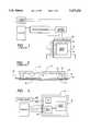
- FIG. 1is a schematic diagram of a prior art active matrix vacuum fluorescent display with external control circuitry
- FIG. 2is a cross section along line 2--2 of the display of FIG. 1;
- FIG. 3is a schematic diagram of an active matrix vacuum fluorescent display with internal control circuitry coupled to external inputs according to the invention.
- FIG. 4is a detailed block diagram of the contents of a silicon substrate of the display of FIG. 3.
- FIG. 1depicts a system using an AMVF array controlled by external circuitry comprising a microprocessor which receives inputs representing vehicle parameters and control signals and decodes the signals to determine which pixels of the array should be illuminated to present the information.
- Drivers responsive to the control signalsapply energizing voltages to the AMVF array via a large number of pins in the display lead frame. The drivers must deliver high voltages to achieve sufficient display brightness. A power supply affords the necessary voltages to the microprocessor and to the drivers. Diagnostic circuitry verifies that the driver outputs are consistent with the pixel energization selected by the microprocessor.
- FIG. 2The construction of such an AMVFD, as shown in FIG. 2, comprises an evacuated glass envelope 10 having a lower glass substrate 12, an upper glass cover 14, and glass frit sealer 16 forming side walls. Filaments 17 are suspended near the top glass.
- the bottom glass 12defines a mounting surface bearing a silicon substrate 18 secured to the glass by epoxy adhesive 20.
- Conductive traces 22 on the glass mounting surfaceare connected to pads on the silicon substrate 18 by wire bonds 24.
- the traces 22extend to a lead frame 26 and are connected to pins 28.
- the lead frameextends through the sealer 16 and the pins thus protrude outwardly from the envelope for connection to the external circuit. Since the large number of columns and rows of the display require many pins 28, the envelope must be large enough to accommodate them.
- FIG. 3provides an overview of the improved AMVFD according to the preferred embodiment of the invention.
- the envelope 10'has essentially the same structure as that described above except that it has relatively few pins.
- the silicon substrate 18'contains not only the AMVF array, but also the microprocessor and the driver or level shifting and address decoder circuit.
- the inputs and external control signalsare few in number and are connected directly to the substrate 18' via the pins 28. Thus the pin count is low and the envelope can be made small. All the numerous connections from the driver to the rows and columns of the array are carried out by conductors integrated in the silicon substrate.
- a power supplydelivers logic level voltage, about 5 volts, as well as pixel drive (or anode) voltage, say, about 50 volts, to the substrate.
- the microprocessorincludes a CPU, a variety of memory units comprising RAM, ROM and EEPROM, a control for handling resets and interrupt requests, and interface elements including a class II or UART serial interface, A/D ports, I/O ports, and a timer.
- the memory componentsare configured according to the specific application.
- the majority of the product softwarecan be mask programmed into microprocessor ROM, with individual product variations being stored in the EEPROM.
- the class II serial bus interfaceis compatible with a vehicle communication bus and it allows the microprocessor to communicate with the external circuitry to determine the proper graphics to display. If desired a high speed serial synchronous data interface can be used with or instead of the slower Class II or UART interface.
- the serial interfacefor example, would be useful to rapidly receive map data for display of a map for navigational purposes.
- the A/D portsreceive vehicle system voltage and other analog values such as fuel level, temperature, and a control signal from a dimmer potentiometer.
- the I/O portsreceive discrete inputs from the vehicle which denote various switch states such as turn signal, brake warning, high beam or other telltale signals.
- the timerreceives a pulsed speedometer signal and determines speed from the pulse period, and also provides a number of timing signals used internally.
- the control componentreceives interrupt requests and a reset signal. While the number of input pins required on the envelope depends of the specific application, generally about 30 pins is sufficient to supply the display, compared to over 200 pins used by the prior art configuration for a 40 by 64 pixel display. A larger display would require the same small number of pins. This drastic reduction of pin count allows the display package to be much smaller.
- the level shift and address decoderis under control of the microprocessor and comprises the interface between the microprocessor and the AMVF array. It addresses the pixels to be illuminated and applies sufficient voltage to the selected anodes to illuminate them.
- the addressing of the AMVF arrayis essentially the same as addressing a static RAM and is done by multiplexing. The required high voltage is on the order of 50 volts or more and thus the voltage level must be increased by about an order of magnitude.
- Diagnostic circuitryis also included on the substrate to check the microprocessor operation and to verify that the energized pixels are indeed those which are selected by the microprocessor to be illuminated.
Landscapes
- Engineering & Computer Science (AREA)
- Physics & Mathematics (AREA)
- Computer Hardware Design (AREA)
- General Physics & Mathematics (AREA)
- Theoretical Computer Science (AREA)
- Control Of Indicators Other Than Cathode Ray Tubes (AREA)
Abstract
Description
This invention relates to vacuum fluorescent displays and particularly to such a display having a silicon substrate containing an active matrix anode array including anode drivers and a microprocessor control for the display.
Automotive vehicles often use vacuum fluorescent displays (VFDs) as instrumentation for providing vehicle speed and other information to the operator. The display is housed in a vacuum tube having a lead frame defining pins connected to various anode portions. In external control circuitry, typically speed data, various switch states, fuel level, dimmer control, and other digital or analog information is fed to a microprocessor which determines which anode portions should be illuminated to convey the information in an orderly manner. Many outputs are then coupled from the microprocessor to the pins via drivers which supply the required voltage level for the desired illumination intensity.
Generally such VF displays use fixed segment anodes to display graphic data. Each anode segment, which comprises one of the individual graphic segments when activated, is connected via a lead frame pin of the VFD to the external control circuitry which is physically separate from the display. This control circuitry is effective to impose the correct "on" voltage on each anode segment to be illuminated and an "off" voltage on the remaining segments. Such fixed segment displays are generally dedicated to specific information, so that a large array of such displays would be required to afford all the information which might be desirably provided to the operator. In the case of direct viewing of the display, limitations in instrument panel space prohibits such expanses of display area. Moreover, when the display is used in conjunction with a head up display (HUD), very small displays are required to minimize the HUD package size. A limiting factor in size reduction is the number of lead frame pins for connection to the outside circuit device. In practice, the anode segments are multiplexed (and thus less bright) to reduce the number of VF driver outputs required and/or to reduce the number of pins to keep the package size smaller.
To show a large amount of information in a small display space it has been proposed to utilize a reconfigurable display which is capable of revealing several types of information on a time sharing basis. It is known to use conventional dot matrix displays for this purpose but these have had limited brightness due to multiplexing requirements. Heretofore such displays have driven by pinning out each row and column of the array to a lead frame for connection to external driving circuitry. Each row or column uses two pins so that, for example, a 40×64pixel array requires more than 200 pins, thereby limiting size reduction attempts.
An improvement over the conventional dot matrix display in terms of brightness is the active matrix vacuum fluorescent display (AMVFD) which includes a silicon substrate containing pixel and display multiplexing circuitry. By sending the appropriate data to the device data lines and power supply lines, the pixels on the device are turned on or off. A variety of reconfigurable graphics such as characters, numbers, ISO symbols, map data, etc. can be displayed. The construction of such AMVFDs comprises an evacuated glass envelope having a mounting surface bearing the silicon substrate and conductive traces extending across the mounting surface from the substrate to a lead frame which affords connections to external circuitry. Wire bonds couple the conductive traces to the silicon substrate, and conductive traces extending across the mounting surface from the substrate to a lead frame which affords connections to external circuitry. Wire bonds couple the conductive traces to the silicon substrate. Filaments necessary to VFD operation are also included within the envelope. Self standing grids are not needed since a coplanar grid on the anode surface is employed. Details of such displays are disclosed in the papers "MOS-Addressed VFD Character Display Incorporating Static RAM", Uemura et al, SID 85 Digest, 362 and "High-Resolution VFD On-a-Chip", Yoshimura et al, SID 86 Digest, 403, which are incorporated herein by reference. Disadvantages of the AMVFD are the high cost of the silicon substrate and the need for individual pins for each row and column, as in the conventional dot matrix display. It is desirable, however to obtain the advantages of the AMVFD in a smaller size and at a lower cost.
It is therefore an object of the invention to take advantage of the brightness and reconfiguration properties of the active matrix VFD while minimizing the cost of the resulting display. Another object is to reduce the number of pins required for connection to external circuitry, thus allowing the display size to be reduced.
The invention is carried out by employing a silicon substrate mounted in the glass envelope of the display, the substrate containing an AMVFD, a microprocessor for controlling the AMVFD, drivers and level shifting circuitry for supplying the correct voltage to each pixel of the display, and interface circuits. Only minimal external circuitry is needed to supply power, vehicle parameters and control data to the interface circuits and thus relatively few connection pins are required to handle the inputs. A lead frame contains the connecting pins at the envelope periphery, and aluminum traces on the glass extend from the pins to the edge of the silicon substrate and are wire bonded to pads on the substrate. Row and column drivers for the anode array are embodied on the same substrate and thus connected to the array through numerous conductive paths in the substrate. The resulting small number of pins in the lead frame permits the display to be made small. Economies due to small display size and the reduction of external circuitry help to make the display practical. The drivers include level shifting so that a low signal level voltage can be increased to a high voltage for anode energization necessary for high display intensity.
The above and other advantages of the invention will become more apparent from the following description taken in conjunction with the accompanying drawings wherein like references refer to like parts and wherein:
FIG. 1 is a schematic diagram of a prior art active matrix vacuum fluorescent display with external control circuitry;
FIG. 2 is a cross section alongline 2--2 of the display of FIG. 1;
FIG. 3 is a schematic diagram of an active matrix vacuum fluorescent display with internal control circuitry coupled to external inputs according to the invention; and
FIG. 4 is a detailed block diagram of the contents of a silicon substrate of the display of FIG. 3.
Prior AMVFD technology is discussed first to provide a reference for comparison with the improvement according to the invention. FIG. 1 depicts a system using an AMVF array controlled by external circuitry comprising a microprocessor which receives inputs representing vehicle parameters and control signals and decodes the signals to determine which pixels of the array should be illuminated to present the information. Drivers responsive to the control signals apply energizing voltages to the AMVF array via a large number of pins in the display lead frame. The drivers must deliver high voltages to achieve sufficient display brightness. A power supply affords the necessary voltages to the microprocessor and to the drivers. Diagnostic circuitry verifies that the driver outputs are consistent with the pixel energization selected by the microprocessor.
The construction of such an AMVFD, as shown in FIG. 2, comprises an evacuatedglass envelope 10 having alower glass substrate 12, anupper glass cover 14, and glassfrit sealer 16 forming side walls.Filaments 17 are suspended near the top glass. Thebottom glass 12 defines a mounting surface bearing asilicon substrate 18 secured to the glass byepoxy adhesive 20.Conductive traces 22 on the glass mounting surface are connected to pads on thesilicon substrate 18 bywire bonds 24. Thetraces 22 extend to alead frame 26 and are connected topins 28. The lead frame extends through thesealer 16 and the pins thus protrude outwardly from the envelope for connection to the external circuit. Since the large number of columns and rows of the display requiremany pins 28, the envelope must be large enough to accommodate them.
FIG. 3 provides an overview of the improved AMVFD according to the preferred embodiment of the invention. There the envelope 10' has essentially the same structure as that described above except that it has relatively few pins. The silicon substrate 18' contains not only the AMVF array, but also the microprocessor and the driver or level shifting and address decoder circuit. The inputs and external control signals are few in number and are connected directly to the substrate 18' via thepins 28. Thus the pin count is low and the envelope can be made small. All the numerous connections from the driver to the rows and columns of the array are carried out by conductors integrated in the silicon substrate. A power supply delivers logic level voltage, about 5 volts, as well as pixel drive (or anode) voltage, say, about 50 volts, to the substrate.
The combined microprocessor, level shifter and AMVF array on the silicon substrate are shown in more detail in FIG. 4. Preferably the microprocessor includes a CPU, a variety of memory units comprising RAM, ROM and EEPROM, a control for handling resets and interrupt requests, and interface elements including a class II or UART serial interface, A/D ports, I/O ports, and a timer. The memory components are configured according to the specific application. The majority of the product software can be mask programmed into microprocessor ROM, with individual product variations being stored in the EEPROM. The class II serial bus interface is compatible with a vehicle communication bus and it allows the microprocessor to communicate with the external circuitry to determine the proper graphics to display. If desired a high speed serial synchronous data interface can be used with or instead of the slower Class II or UART interface. The serial interface, for example, would be useful to rapidly receive map data for display of a map for navigational purposes.
The A/D ports receive vehicle system voltage and other analog values such as fuel level, temperature, and a control signal from a dimmer potentiometer. The I/O ports receive discrete inputs from the vehicle which denote various switch states such as turn signal, brake warning, high beam or other telltale signals. The timer receives a pulsed speedometer signal and determines speed from the pulse period, and also provides a number of timing signals used internally. The control component receives interrupt requests and a reset signal. While the number of input pins required on the envelope depends of the specific application, generally about 30 pins is sufficient to supply the display, compared to over 200 pins used by the prior art configuration for a 40 by 64 pixel display. A larger display would require the same small number of pins. This drastic reduction of pin count allows the display package to be much smaller.
The level shift and address decoder is under control of the microprocessor and comprises the interface between the microprocessor and the AMVF array. It addresses the pixels to be illuminated and applies sufficient voltage to the selected anodes to illuminate them. The addressing of the AMVF array is essentially the same as addressing a static RAM and is done by multiplexing. The required high voltage is on the order of 50 volts or more and thus the voltage level must be increased by about an order of magnitude.
Diagnostic circuitry is also included on the substrate to check the microprocessor operation and to verify that the energized pixels are indeed those which are selected by the microprocessor to be illuminated.
It will thus be seen that by reason of integrating the anode array and the control circuitry on the same substrate that a much smaller display size is possible and the external support circuitry is drastically reduced, thereby improving both the cost of such a display but its utility as well.
Claims (3)
1. An integrated vacuum fluorescent display comprising:
a vacuum fluorescent display tube having cathode elements;
a support surface of the display tube having a silicon substrate spaced from the cathode elements, the substrate containing an active matrix anode array, a microprocessor, and an interface coupling the microprocessor to the array;
the interface including anode drivers for controlling pixel activation in response to signals from the microprocessor; and
the silicon substrate further containing conductive paths for connecting the interface to the microprocessor and to the anode array.
2. The invention as defined in claim 1 wherein terminals at an edge of the support surface are connected to the microprocessor and wherein logic level and anode voltage, control data and display parameters are fed to the microprocessor via said terminals.
3. The invention as defined in claim 2 wherein the interface includes level shifting circuitry supplied by the logic level and anode voltage for converting low voltage data to high voltage data, which is an order of magnitude greater than the logic level voltages used for microprocessor operation.
Priority Applications (1)
| Application Number | Priority Date | Filing Date | Title |
|---|---|---|---|
| US08/270,877US5473222A (en) | 1994-07-05 | 1994-07-05 | Active matrix vacuum fluorescent display with microprocessor integration |
Applications Claiming Priority (1)
| Application Number | Priority Date | Filing Date | Title |
|---|---|---|---|
| US08/270,877US5473222A (en) | 1994-07-05 | 1994-07-05 | Active matrix vacuum fluorescent display with microprocessor integration |
Publications (1)
| Publication Number | Publication Date |
|---|---|
| US5473222Atrue US5473222A (en) | 1995-12-05 |
Family
ID=23033200
Family Applications (1)
| Application Number | Title | Priority Date | Filing Date |
|---|---|---|---|
| US08/270,877Expired - LifetimeUS5473222A (en) | 1994-07-05 | 1994-07-05 | Active matrix vacuum fluorescent display with microprocessor integration |
Country Status (1)
| Country | Link |
|---|---|
| US (1) | US5473222A (en) |
Cited By (81)
| Publication number | Priority date | Publication date | Assignee | Title |
|---|---|---|---|---|
| US5684368A (en)* | 1996-06-10 | 1997-11-04 | Motorola | Smart driver for an array of LEDs |
| US5861712A (en)* | 1995-08-25 | 1999-01-19 | International Business Machines Corporation | Electron source with grid spacer |
| US5877735A (en)* | 1995-06-23 | 1999-03-02 | Planar Systems, Inc. | Substrate carriers for electroluminescent displays |
| US5917277A (en)* | 1995-08-25 | 1999-06-29 | International Business Machines Corporation | Electron source including a perforated permanent magnet |
| US5994834A (en)* | 1997-08-22 | 1999-11-30 | Micron Technology, Inc. | Conductive address structure for field emission displays |
| US6002207A (en)* | 1995-08-25 | 1999-12-14 | International Business Machines Corporation | Electron source with light shutter device |
| US20020033811A1 (en)* | 2000-09-06 | 2002-03-21 | Yazaki Corporation | Drive circuit for vacuum fluorescent display tube |
| US6361392B2 (en) | 1998-07-29 | 2002-03-26 | Micron Technology, Inc. | Extraction grid for field emission displays and method |
| US20020185950A1 (en)* | 2001-06-08 | 2002-12-12 | Sony Corporation And Sony Electronics Inc. | Carbon cathode of a field emission display with in-laid isolation barrier and support |
| US20020185951A1 (en)* | 2001-06-08 | 2002-12-12 | Sony Corporation | Carbon cathode of a field emission display with integrated isolation barrier and support on substrate |
| US20030188169A1 (en)* | 2002-03-27 | 2003-10-02 | Strongin Geoffrey S. | System and method for controlling device-to-device accesses within a computer system |
| US20030209960A1 (en)* | 2002-05-13 | 2003-11-13 | Delphi Technologies, Inc. | Heating element for fluorescent lamps |
| US6710538B1 (en)* | 1998-08-26 | 2004-03-23 | Micron Technology, Inc. | Field emission display having reduced power requirements and method |
| US20040090163A1 (en)* | 2001-06-08 | 2004-05-13 | Sony Corporation | Field emission display utilizing a cathode frame-type gate |
| US20040100184A1 (en)* | 2002-11-27 | 2004-05-27 | Sony Corporation | Spacer-less field emission display |
| US20040104667A1 (en)* | 2001-06-08 | 2004-06-03 | Sony Corporation | Field emission display using gate wires |
| US20040145299A1 (en)* | 2003-01-24 | 2004-07-29 | Sony Corporation | Line patterned gate structure for a field emission display |
| US20040189554A1 (en)* | 2003-03-31 | 2004-09-30 | Sony Corporation | Image display device incorporating driver circuits on active substrate and other methods to reduce interconnects |
| US20040189552A1 (en)* | 2003-03-31 | 2004-09-30 | Sony Corporation | Image display device incorporating driver circuits on active substrate to reduce interconnects |
| US20080110017A1 (en)* | 2006-11-15 | 2008-05-15 | Seiko Epson Corporation | Wiring substrate, method of manufacturing wiring substrate, and electronic apparatus |
| DE102008005221A1 (en)* | 2007-09-17 | 2009-04-23 | Elitegroup Computer Systems Co., Ltd. | Navigation display |
| CN101494021B (en)* | 2008-01-21 | 2010-10-27 | 普诚科技股份有限公司 | Vacuum fluorescent display driving circuit and vacuum fluorescent display |
| US9244280B1 (en) | 2014-03-25 | 2016-01-26 | Rockwell Collins, Inc. | Near eye display system and method for display enhancement or redundancy |
| US9244281B1 (en) | 2013-09-26 | 2016-01-26 | Rockwell Collins, Inc. | Display system and method using a detached combiner |
| US9274339B1 (en) | 2010-02-04 | 2016-03-01 | Rockwell Collins, Inc. | Worn display system and method without requiring real time tracking for boresight precision |
| US9341846B2 (en) | 2012-04-25 | 2016-05-17 | Rockwell Collins Inc. | Holographic wide angle display |
| US9366864B1 (en) | 2011-09-30 | 2016-06-14 | Rockwell Collins, Inc. | System for and method of displaying information without need for a combiner alignment detector |
| US9507150B1 (en) | 2011-09-30 | 2016-11-29 | Rockwell Collins, Inc. | Head up display (HUD) using a bent waveguide assembly |
| US9519089B1 (en) | 2014-01-30 | 2016-12-13 | Rockwell Collins, Inc. | High performance volume phase gratings |
| US9523852B1 (en) | 2012-03-28 | 2016-12-20 | Rockwell Collins, Inc. | Micro collimator system and method for a head up display (HUD) |
| US9674413B1 (en) | 2013-04-17 | 2017-06-06 | Rockwell Collins, Inc. | Vision system and method having improved performance and solar mitigation |
| US9715110B1 (en) | 2014-09-25 | 2017-07-25 | Rockwell Collins, Inc. | Automotive head up display (HUD) |
| US9715067B1 (en) | 2011-09-30 | 2017-07-25 | Rockwell Collins, Inc. | Ultra-compact HUD utilizing waveguide pupil expander with surface relief gratings in high refractive index materials |
| US9933684B2 (en) | 2012-11-16 | 2018-04-03 | Rockwell Collins, Inc. | Transparent waveguide display providing upper and lower fields of view having a specific light output aperture configuration |
| US10088675B1 (en) | 2015-05-18 | 2018-10-02 | Rockwell Collins, Inc. | Turning light pipe for a pupil expansion system and method |
| US10108010B2 (en) | 2015-06-29 | 2018-10-23 | Rockwell Collins, Inc. | System for and method of integrating head up displays and head down displays |
| US10126552B2 (en) | 2015-05-18 | 2018-11-13 | Rockwell Collins, Inc. | Micro collimator system and method for a head up display (HUD) |
| US10156681B2 (en) | 2015-02-12 | 2018-12-18 | Digilens Inc. | Waveguide grating device |
| US10241330B2 (en) | 2014-09-19 | 2019-03-26 | Digilens, Inc. | Method and apparatus for generating input images for holographic waveguide displays |
| US10247943B1 (en) | 2015-05-18 | 2019-04-02 | Rockwell Collins, Inc. | Head up display (HUD) using a light pipe |
| US10295824B2 (en) | 2017-01-26 | 2019-05-21 | Rockwell Collins, Inc. | Head up display with an angled light pipe |
| US10359736B2 (en) | 2014-08-08 | 2019-07-23 | Digilens Inc. | Method for holographic mastering and replication |
| US10509241B1 (en) | 2009-09-30 | 2019-12-17 | Rockwell Collins, Inc. | Optical displays |
| US10545346B2 (en) | 2017-01-05 | 2020-01-28 | Digilens Inc. | Wearable heads up displays |
| US10598932B1 (en) | 2016-01-06 | 2020-03-24 | Rockwell Collins, Inc. | Head up display for integrating views of conformally mapped symbols and a fixed image source |
| US10642058B2 (en) | 2011-08-24 | 2020-05-05 | Digilens Inc. | Wearable data display |
| US10670876B2 (en) | 2011-08-24 | 2020-06-02 | Digilens Inc. | Waveguide laser illuminator incorporating a despeckler |
| US10678053B2 (en) | 2009-04-27 | 2020-06-09 | Digilens Inc. | Diffractive projection apparatus |
| US10690916B2 (en) | 2015-10-05 | 2020-06-23 | Digilens Inc. | Apparatus for providing waveguide displays with two-dimensional pupil expansion |
| US10725312B2 (en) | 2007-07-26 | 2020-07-28 | Digilens Inc. | Laser illumination device |
| US10732569B2 (en) | 2018-01-08 | 2020-08-04 | Digilens Inc. | Systems and methods for high-throughput recording of holographic gratings in waveguide cells |
| US10732407B1 (en) | 2014-01-10 | 2020-08-04 | Rockwell Collins, Inc. | Near eye head up display system and method with fixed combiner |
| US10747982B2 (en) | 2013-07-31 | 2020-08-18 | Digilens Inc. | Method and apparatus for contact image sensing |
| US10795160B1 (en) | 2014-09-25 | 2020-10-06 | Rockwell Collins, Inc. | Systems for and methods of using fold gratings for dual axis expansion |
| US10859768B2 (en) | 2016-03-24 | 2020-12-08 | Digilens Inc. | Method and apparatus for providing a polarization selective holographic waveguide device |
| US10890707B2 (en) | 2016-04-11 | 2021-01-12 | Digilens Inc. | Holographic waveguide apparatus for structured light projection |
| US10914950B2 (en) | 2018-01-08 | 2021-02-09 | Digilens Inc. | Waveguide architectures and related methods of manufacturing |
| US10942430B2 (en) | 2017-10-16 | 2021-03-09 | Digilens Inc. | Systems and methods for multiplying the image resolution of a pixelated display |
| US11256155B2 (en) | 2012-01-06 | 2022-02-22 | Digilens Inc. | Contact image sensor using switchable Bragg gratings |
| US11300795B1 (en) | 2009-09-30 | 2022-04-12 | Digilens Inc. | Systems for and methods of using fold gratings coordinated with output couplers for dual axis expansion |
| US11307432B2 (en) | 2014-08-08 | 2022-04-19 | Digilens Inc. | Waveguide laser illuminator incorporating a Despeckler |
| US11314084B1 (en) | 2011-09-30 | 2022-04-26 | Rockwell Collins, Inc. | Waveguide combiner system and method with less susceptibility to glare |
| US11320571B2 (en) | 2012-11-16 | 2022-05-03 | Rockwell Collins, Inc. | Transparent waveguide display providing upper and lower fields of view with uniform light extraction |
| US11366316B2 (en) | 2015-05-18 | 2022-06-21 | Rockwell Collins, Inc. | Head up display (HUD) using a light pipe |
| US11378732B2 (en) | 2019-03-12 | 2022-07-05 | DigLens Inc. | Holographic waveguide backlight and related methods of manufacturing |
| US11402801B2 (en) | 2018-07-25 | 2022-08-02 | Digilens Inc. | Systems and methods for fabricating a multilayer optical structure |
| US11442222B2 (en) | 2019-08-29 | 2022-09-13 | Digilens Inc. | Evacuated gratings and methods of manufacturing |
| US11487131B2 (en) | 2011-04-07 | 2022-11-01 | Digilens Inc. | Laser despeckler based on angular diversity |
| US11513350B2 (en) | 2016-12-02 | 2022-11-29 | Digilens Inc. | Waveguide device with uniform output illumination |
| US11543594B2 (en) | 2019-02-15 | 2023-01-03 | Digilens Inc. | Methods and apparatuses for providing a holographic waveguide display using integrated gratings |
| US11681143B2 (en) | 2019-07-29 | 2023-06-20 | Digilens Inc. | Methods and apparatus for multiplying the image resolution and field-of-view of a pixelated display |
| US11726332B2 (en) | 2009-04-27 | 2023-08-15 | Digilens Inc. | Diffractive projection apparatus |
| US11726329B2 (en) | 2015-01-12 | 2023-08-15 | Digilens Inc. | Environmentally isolated waveguide display |
| US11747568B2 (en) | 2019-06-07 | 2023-09-05 | Digilens Inc. | Waveguides incorporating transmissive and reflective gratings and related methods of manufacturing |
| US12092914B2 (en) | 2018-01-08 | 2024-09-17 | Digilens Inc. | Systems and methods for manufacturing waveguide cells |
| US12140764B2 (en) | 2019-02-15 | 2024-11-12 | Digilens Inc. | Wide angle waveguide display |
| US12158612B2 (en) | 2021-03-05 | 2024-12-03 | Digilens Inc. | Evacuated periodic structures and methods of manufacturing |
| US12210153B2 (en) | 2019-01-14 | 2025-01-28 | Digilens Inc. | Holographic waveguide display with light control layer |
| US12306585B2 (en) | 2018-01-08 | 2025-05-20 | Digilens Inc. | Methods for fabricating optical waveguides |
| US12399326B2 (en) | 2021-01-07 | 2025-08-26 | Digilens Inc. | Grating structures for color waveguides |
| US12397477B2 (en) | 2019-02-05 | 2025-08-26 | Digilens Inc. | Methods for compensating for optical surface nonuniformity |
Citations (9)
| Publication number | Priority date | Publication date | Assignee | Title |
|---|---|---|---|---|
| US4859913A (en)* | 1984-05-01 | 1989-08-22 | Xerox Corporation | Vacuum fluorescent printing device |
| US5099178A (en)* | 1990-08-20 | 1992-03-24 | Ford Motor Company | Method and system for controlling the brightness of a vacuum fluorescent display |
| US5151632A (en)* | 1991-03-22 | 1992-09-29 | General Motors Corporation | Flat panel emissive display with redundant circuit |
| US5155413A (en)* | 1990-08-20 | 1992-10-13 | Ford Motor Company | Method and system for controlling the brightness of a vacuum fluorescent display |
| US5177406A (en)* | 1991-04-29 | 1993-01-05 | General Motors Corporation | Active matrix vacuum fluorescent display with compensation for variable phosphor efficiency |
| US5258325A (en)* | 1990-12-31 | 1993-11-02 | Kopin Corporation | Method for manufacturing a semiconductor device using a circuit transfer film |
| US5345141A (en)* | 1993-03-29 | 1994-09-06 | Motorola, Inc. | Single substrate, vacuum fluorescent display |
| US5376561A (en)* | 1990-12-31 | 1994-12-27 | Kopin Corporation | High density electronic circuit modules |
| US5426526A (en)* | 1991-04-05 | 1995-06-20 | Sharp Kabushiki Kaisha | Reflection type single crystal silicon substrate liquid crystal display device and system |
- 1994
- 1994-07-05USUS08/270,877patent/US5473222A/ennot_activeExpired - Lifetime
Patent Citations (9)
| Publication number | Priority date | Publication date | Assignee | Title |
|---|---|---|---|---|
| US4859913A (en)* | 1984-05-01 | 1989-08-22 | Xerox Corporation | Vacuum fluorescent printing device |
| US5099178A (en)* | 1990-08-20 | 1992-03-24 | Ford Motor Company | Method and system for controlling the brightness of a vacuum fluorescent display |
| US5155413A (en)* | 1990-08-20 | 1992-10-13 | Ford Motor Company | Method and system for controlling the brightness of a vacuum fluorescent display |
| US5258325A (en)* | 1990-12-31 | 1993-11-02 | Kopin Corporation | Method for manufacturing a semiconductor device using a circuit transfer film |
| US5376561A (en)* | 1990-12-31 | 1994-12-27 | Kopin Corporation | High density electronic circuit modules |
| US5151632A (en)* | 1991-03-22 | 1992-09-29 | General Motors Corporation | Flat panel emissive display with redundant circuit |
| US5426526A (en)* | 1991-04-05 | 1995-06-20 | Sharp Kabushiki Kaisha | Reflection type single crystal silicon substrate liquid crystal display device and system |
| US5177406A (en)* | 1991-04-29 | 1993-01-05 | General Motors Corporation | Active matrix vacuum fluorescent display with compensation for variable phosphor efficiency |
| US5345141A (en)* | 1993-03-29 | 1994-09-06 | Motorola, Inc. | Single substrate, vacuum fluorescent display |
Non-Patent Citations (4)
| Title |
|---|
| "High-Resolution VFD On-a-Chip", Masahiro Yoshimura, Katsumasa Fujii, Schin'ichi Tanka, 1986 SID International Symposium, Digest of Technical Papers, First Edition, pp. 403-406. |
| "MOS-Addressed VFD Character Display Incorporating Static RAM," Masahiro Yoshimura, Katsumasa Fujii, and Schin'ichi Tanaka, Sashiro Uemura, Makoto Horie, 1985 SID International Symposium, Digest of Technical Papers, pp. 362-365, 1985. |
| High Resolution VFD On a Chip , Masahiro Yoshimura, Katsumasa Fujii, Schin ichi Tanka, 1986 SID International Symposium, Digest of Technical Papers, First Edition, pp. 403 406.* |
| MOS Addressed VFD Character Display Incorporating Static RAM, Masahiro Yoshimura, Katsumasa Fujii, and Schin ichi Tanaka, Sashiro Uemura, Makoto Horie, 1985 SID International Symposium, Digest of Technical Papers, pp. 362 365, 1985.* |
Cited By (135)
| Publication number | Priority date | Publication date | Assignee | Title |
|---|---|---|---|---|
| US5877735A (en)* | 1995-06-23 | 1999-03-02 | Planar Systems, Inc. | Substrate carriers for electroluminescent displays |
| US5861712A (en)* | 1995-08-25 | 1999-01-19 | International Business Machines Corporation | Electron source with grid spacer |
| US5917277A (en)* | 1995-08-25 | 1999-06-29 | International Business Machines Corporation | Electron source including a perforated permanent magnet |
| US6002207A (en)* | 1995-08-25 | 1999-12-14 | International Business Machines Corporation | Electron source with light shutter device |
| US5684368A (en)* | 1996-06-10 | 1997-11-04 | Motorola | Smart driver for an array of LEDs |
| US5994834A (en)* | 1997-08-22 | 1999-11-30 | Micron Technology, Inc. | Conductive address structure for field emission displays |
| US6361392B2 (en) | 1998-07-29 | 2002-03-26 | Micron Technology, Inc. | Extraction grid for field emission displays and method |
| US20060152134A1 (en)* | 1998-08-26 | 2006-07-13 | Micron Technology, Inc. | Field emission display having reduced power requirements and method |
| US20040169453A1 (en)* | 1998-08-26 | 2004-09-02 | Ahn Kie Y. | Field emission display having reduced power requirements and method |
| US7042148B2 (en) | 1998-08-26 | 2006-05-09 | Micron Technology, Inc. | Field emission display having reduced power requirements and method |
| US6953375B2 (en) | 1998-08-26 | 2005-10-11 | Micron Technology, Inc. | Manufacturing method of a field emission display having porous silicon dioxide insulating layer |
| US6710538B1 (en)* | 1998-08-26 | 2004-03-23 | Micron Technology, Inc. | Field emission display having reduced power requirements and method |
| US6835111B2 (en) | 1998-08-26 | 2004-12-28 | Micron Technology, Inc. | Field emission display having porous silicon dioxide layer |
| US20040189175A1 (en)* | 1998-08-26 | 2004-09-30 | Ahn Kie Y. | Field emission display having reduced power requirements and method |
| US20020033811A1 (en)* | 2000-09-06 | 2002-03-21 | Yazaki Corporation | Drive circuit for vacuum fluorescent display tube |
| US7002290B2 (en) | 2001-06-08 | 2006-02-21 | Sony Corporation | Carbon cathode of a field emission display with integrated isolation barrier and support on substrate |
| US20020185950A1 (en)* | 2001-06-08 | 2002-12-12 | Sony Corporation And Sony Electronics Inc. | Carbon cathode of a field emission display with in-laid isolation barrier and support |
| US20040104667A1 (en)* | 2001-06-08 | 2004-06-03 | Sony Corporation | Field emission display using gate wires |
| US7118439B2 (en) | 2001-06-08 | 2006-10-10 | Sony Corporation | Field emission display utilizing a cathode frame-type gate and anode with alignment method |
| US20020185951A1 (en)* | 2001-06-08 | 2002-12-12 | Sony Corporation | Carbon cathode of a field emission display with integrated isolation barrier and support on substrate |
| US20040090163A1 (en)* | 2001-06-08 | 2004-05-13 | Sony Corporation | Field emission display utilizing a cathode frame-type gate |
| US20050179397A1 (en)* | 2001-06-08 | 2005-08-18 | Sony Corporation | Field emission display utilizing a cathode frame-type gate and anode with alignment method |
| US6940219B2 (en) | 2001-06-08 | 2005-09-06 | Sony Corporation | Field emission display utilizing a cathode frame-type gate |
| US6989631B2 (en) | 2001-06-08 | 2006-01-24 | Sony Corporation | Carbon cathode of a field emission display with in-laid isolation barrier and support |
| US20030188169A1 (en)* | 2002-03-27 | 2003-10-02 | Strongin Geoffrey S. | System and method for controlling device-to-device accesses within a computer system |
| US6833657B2 (en) | 2002-05-13 | 2004-12-21 | Delphi Technologies, Inc. | Heating element for fluorescent lamps |
| US20030209960A1 (en)* | 2002-05-13 | 2003-11-13 | Delphi Technologies, Inc. | Heating element for fluorescent lamps |
| US7012582B2 (en) | 2002-11-27 | 2006-03-14 | Sony Corporation | Spacer-less field emission display |
| US20040100184A1 (en)* | 2002-11-27 | 2004-05-27 | Sony Corporation | Spacer-less field emission display |
| US20040145299A1 (en)* | 2003-01-24 | 2004-07-29 | Sony Corporation | Line patterned gate structure for a field emission display |
| US20040189552A1 (en)* | 2003-03-31 | 2004-09-30 | Sony Corporation | Image display device incorporating driver circuits on active substrate to reduce interconnects |
| US7071629B2 (en)* | 2003-03-31 | 2006-07-04 | Sony Corporation | Image display device incorporating driver circuits on active substrate and other methods to reduce interconnects |
| US20040189554A1 (en)* | 2003-03-31 | 2004-09-30 | Sony Corporation | Image display device incorporating driver circuits on active substrate and other methods to reduce interconnects |
| US8127438B2 (en)* | 2006-11-15 | 2012-03-06 | Seiko Epson Corporation | Wiring substrate, method of manufacturing wiring substrate, and electronic apparatus |
| US20080110017A1 (en)* | 2006-11-15 | 2008-05-15 | Seiko Epson Corporation | Wiring substrate, method of manufacturing wiring substrate, and electronic apparatus |
| US10725312B2 (en) | 2007-07-26 | 2020-07-28 | Digilens Inc. | Laser illumination device |
| DE102008005221A1 (en)* | 2007-09-17 | 2009-04-23 | Elitegroup Computer Systems Co., Ltd. | Navigation display |
| CN101494021B (en)* | 2008-01-21 | 2010-10-27 | 普诚科技股份有限公司 | Vacuum fluorescent display driving circuit and vacuum fluorescent display |
| US11175512B2 (en) | 2009-04-27 | 2021-11-16 | Digilens Inc. | Diffractive projection apparatus |
| US11726332B2 (en) | 2009-04-27 | 2023-08-15 | Digilens Inc. | Diffractive projection apparatus |
| US10678053B2 (en) | 2009-04-27 | 2020-06-09 | Digilens Inc. | Diffractive projection apparatus |
| US10509241B1 (en) | 2009-09-30 | 2019-12-17 | Rockwell Collins, Inc. | Optical displays |
| US11300795B1 (en) | 2009-09-30 | 2022-04-12 | Digilens Inc. | Systems for and methods of using fold gratings coordinated with output couplers for dual axis expansion |
| US9274339B1 (en) | 2010-02-04 | 2016-03-01 | Rockwell Collins, Inc. | Worn display system and method without requiring real time tracking for boresight precision |
| US11487131B2 (en) | 2011-04-07 | 2022-11-01 | Digilens Inc. | Laser despeckler based on angular diversity |
| US12306418B2 (en) | 2011-08-24 | 2025-05-20 | Rockwell Collins, Inc. | Wearable data display |
| US10670876B2 (en) | 2011-08-24 | 2020-06-02 | Digilens Inc. | Waveguide laser illuminator incorporating a despeckler |
| US10642058B2 (en) | 2011-08-24 | 2020-05-05 | Digilens Inc. | Wearable data display |
| US11287666B2 (en) | 2011-08-24 | 2022-03-29 | Digilens, Inc. | Wearable data display |
| US11314084B1 (en) | 2011-09-30 | 2022-04-26 | Rockwell Collins, Inc. | Waveguide combiner system and method with less susceptibility to glare |
| US9715067B1 (en) | 2011-09-30 | 2017-07-25 | Rockwell Collins, Inc. | Ultra-compact HUD utilizing waveguide pupil expander with surface relief gratings in high refractive index materials |
| US9977247B1 (en) | 2011-09-30 | 2018-05-22 | Rockwell Collins, Inc. | System for and method of displaying information without need for a combiner alignment detector |
| US9599813B1 (en) | 2011-09-30 | 2017-03-21 | Rockwell Collins, Inc. | Waveguide combiner system and method with less susceptibility to glare |
| US10401620B1 (en) | 2011-09-30 | 2019-09-03 | Rockwell Collins, Inc. | Waveguide combiner system and method with less susceptibility to glare |
| US9507150B1 (en) | 2011-09-30 | 2016-11-29 | Rockwell Collins, Inc. | Head up display (HUD) using a bent waveguide assembly |
| US9366864B1 (en) | 2011-09-30 | 2016-06-14 | Rockwell Collins, Inc. | System for and method of displaying information without need for a combiner alignment detector |
| US11256155B2 (en) | 2012-01-06 | 2022-02-22 | Digilens Inc. | Contact image sensor using switchable Bragg gratings |
| US9523852B1 (en) | 2012-03-28 | 2016-12-20 | Rockwell Collins, Inc. | Micro collimator system and method for a head up display (HUD) |
| US11460621B2 (en) | 2012-04-25 | 2022-10-04 | Rockwell Collins, Inc. | Holographic wide angle display |
| US10690915B2 (en) | 2012-04-25 | 2020-06-23 | Rockwell Collins, Inc. | Holographic wide angle display |
| US9341846B2 (en) | 2012-04-25 | 2016-05-17 | Rockwell Collins Inc. | Holographic wide angle display |
| US11815781B2 (en) | 2012-11-16 | 2023-11-14 | Rockwell Collins, Inc. | Transparent waveguide display |
| US9933684B2 (en) | 2012-11-16 | 2018-04-03 | Rockwell Collins, Inc. | Transparent waveguide display providing upper and lower fields of view having a specific light output aperture configuration |
| US20180373115A1 (en)* | 2012-11-16 | 2018-12-27 | Digilens, Inc. | Transparent Waveguide Display |
| US11448937B2 (en) | 2012-11-16 | 2022-09-20 | Digilens Inc. | Transparent waveguide display for tiling a display having plural optical powers using overlapping and offset FOV tiles |
| US12405507B2 (en) | 2012-11-16 | 2025-09-02 | Digilens Inc. | Transparent waveguide display with grating lamina that both couple and extract modulated light |
| US12276895B2 (en) | 2012-11-16 | 2025-04-15 | Rockwell Collins, Inc. | Transparent waveguide display with passive expander input bragg gratings with different angular diffraction efficiencies |
| US11320571B2 (en) | 2012-11-16 | 2022-05-03 | Rockwell Collins, Inc. | Transparent waveguide display providing upper and lower fields of view with uniform light extraction |
| US9674413B1 (en) | 2013-04-17 | 2017-06-06 | Rockwell Collins, Inc. | Vision system and method having improved performance and solar mitigation |
| US9679367B1 (en) | 2013-04-17 | 2017-06-13 | Rockwell Collins, Inc. | HUD system and method with dynamic light exclusion |
| US10747982B2 (en) | 2013-07-31 | 2020-08-18 | Digilens Inc. | Method and apparatus for contact image sensing |
| US9244281B1 (en) | 2013-09-26 | 2016-01-26 | Rockwell Collins, Inc. | Display system and method using a detached combiner |
| US10732407B1 (en) | 2014-01-10 | 2020-08-04 | Rockwell Collins, Inc. | Near eye head up display system and method with fixed combiner |
| US9519089B1 (en) | 2014-01-30 | 2016-12-13 | Rockwell Collins, Inc. | High performance volume phase gratings |
| US9244280B1 (en) | 2014-03-25 | 2016-01-26 | Rockwell Collins, Inc. | Near eye display system and method for display enhancement or redundancy |
| US9766465B1 (en) | 2014-03-25 | 2017-09-19 | Rockwell Collins, Inc. | Near eye display system and method for display enhancement or redundancy |
| US11307432B2 (en) | 2014-08-08 | 2022-04-19 | Digilens Inc. | Waveguide laser illuminator incorporating a Despeckler |
| US11709373B2 (en) | 2014-08-08 | 2023-07-25 | Digilens Inc. | Waveguide laser illuminator incorporating a despeckler |
| US10359736B2 (en) | 2014-08-08 | 2019-07-23 | Digilens Inc. | Method for holographic mastering and replication |
| US11726323B2 (en) | 2014-09-19 | 2023-08-15 | Digilens Inc. | Method and apparatus for generating input images for holographic waveguide displays |
| US10241330B2 (en) | 2014-09-19 | 2019-03-26 | Digilens, Inc. | Method and apparatus for generating input images for holographic waveguide displays |
| US9715110B1 (en) | 2014-09-25 | 2017-07-25 | Rockwell Collins, Inc. | Automotive head up display (HUD) |
| US10795160B1 (en) | 2014-09-25 | 2020-10-06 | Rockwell Collins, Inc. | Systems for and methods of using fold gratings for dual axis expansion |
| US11579455B2 (en) | 2014-09-25 | 2023-02-14 | Rockwell Collins, Inc. | Systems for and methods of using fold gratings for dual axis expansion using polarized light for wave plates on waveguide faces |
| US11740472B2 (en) | 2015-01-12 | 2023-08-29 | Digilens Inc. | Environmentally isolated waveguide display |
| US11726329B2 (en) | 2015-01-12 | 2023-08-15 | Digilens Inc. | Environmentally isolated waveguide display |
| US11703645B2 (en) | 2015-02-12 | 2023-07-18 | Digilens Inc. | Waveguide grating device |
| US10156681B2 (en) | 2015-02-12 | 2018-12-18 | Digilens Inc. | Waveguide grating device |
| US12379547B2 (en) | 2015-02-12 | 2025-08-05 | Digilens Inc. | Waveguide grating device |
| US10527797B2 (en) | 2015-02-12 | 2020-01-07 | Digilens Inc. | Waveguide grating device |
| US10746989B2 (en) | 2015-05-18 | 2020-08-18 | Rockwell Collins, Inc. | Micro collimator system and method for a head up display (HUD) |
| US10247943B1 (en) | 2015-05-18 | 2019-04-02 | Rockwell Collins, Inc. | Head up display (HUD) using a light pipe |
| US10088675B1 (en) | 2015-05-18 | 2018-10-02 | Rockwell Collins, Inc. | Turning light pipe for a pupil expansion system and method |
| US10698203B1 (en) | 2015-05-18 | 2020-06-30 | Rockwell Collins, Inc. | Turning light pipe for a pupil expansion system and method |
| US10126552B2 (en) | 2015-05-18 | 2018-11-13 | Rockwell Collins, Inc. | Micro collimator system and method for a head up display (HUD) |
| US11366316B2 (en) | 2015-05-18 | 2022-06-21 | Rockwell Collins, Inc. | Head up display (HUD) using a light pipe |
| US10108010B2 (en) | 2015-06-29 | 2018-10-23 | Rockwell Collins, Inc. | System for and method of integrating head up displays and head down displays |
| US11754842B2 (en) | 2015-10-05 | 2023-09-12 | Digilens Inc. | Apparatus for providing waveguide displays with two-dimensional pupil expansion |
| US12405471B2 (en) | 2015-10-05 | 2025-09-02 | Digilens Inc. | Apparatus for providing waveguide displays with two-dimensional pupil expansion |
| US11281013B2 (en) | 2015-10-05 | 2022-03-22 | Digilens Inc. | Apparatus for providing waveguide displays with two-dimensional pupil expansion |
| US10690916B2 (en) | 2015-10-05 | 2020-06-23 | Digilens Inc. | Apparatus for providing waveguide displays with two-dimensional pupil expansion |
| US10598932B1 (en) | 2016-01-06 | 2020-03-24 | Rockwell Collins, Inc. | Head up display for integrating views of conformally mapped symbols and a fixed image source |
| US11215834B1 (en) | 2016-01-06 | 2022-01-04 | Rockwell Collins, Inc. | Head up display for integrating views of conformally mapped symbols and a fixed image source |
| US11604314B2 (en) | 2016-03-24 | 2023-03-14 | Digilens Inc. | Method and apparatus for providing a polarization selective holographic waveguide device |
| US10859768B2 (en) | 2016-03-24 | 2020-12-08 | Digilens Inc. | Method and apparatus for providing a polarization selective holographic waveguide device |
| US10890707B2 (en) | 2016-04-11 | 2021-01-12 | Digilens Inc. | Holographic waveguide apparatus for structured light projection |
| US11513350B2 (en) | 2016-12-02 | 2022-11-29 | Digilens Inc. | Waveguide device with uniform output illumination |
| US12298513B2 (en) | 2016-12-02 | 2025-05-13 | Digilens Inc. | Waveguide device with uniform output illumination |
| US11586046B2 (en) | 2017-01-05 | 2023-02-21 | Digilens Inc. | Wearable heads up displays |
| US11194162B2 (en) | 2017-01-05 | 2021-12-07 | Digilens Inc. | Wearable heads up displays |
| US12248150B2 (en) | 2017-01-05 | 2025-03-11 | Digilens Inc. | Wearable heads up displays |
| US10545346B2 (en) | 2017-01-05 | 2020-01-28 | Digilens Inc. | Wearable heads up displays |
| US10705337B2 (en) | 2017-01-26 | 2020-07-07 | Rockwell Collins, Inc. | Head up display with an angled light pipe |
| US10295824B2 (en) | 2017-01-26 | 2019-05-21 | Rockwell Collins, Inc. | Head up display with an angled light pipe |
| US10942430B2 (en) | 2017-10-16 | 2021-03-09 | Digilens Inc. | Systems and methods for multiplying the image resolution of a pixelated display |
| US12352960B2 (en) | 2018-01-08 | 2025-07-08 | Digilens Inc. | Waveguide architectures and related methods of manufacturing |
| US10914950B2 (en) | 2018-01-08 | 2021-02-09 | Digilens Inc. | Waveguide architectures and related methods of manufacturing |
| US12092914B2 (en) | 2018-01-08 | 2024-09-17 | Digilens Inc. | Systems and methods for manufacturing waveguide cells |
| US12366823B2 (en) | 2018-01-08 | 2025-07-22 | Digilens Inc. | Systems and methods for high-throughput recording of holographic gratings in waveguide cells |
| US10732569B2 (en) | 2018-01-08 | 2020-08-04 | Digilens Inc. | Systems and methods for high-throughput recording of holographic gratings in waveguide cells |
| US12306585B2 (en) | 2018-01-08 | 2025-05-20 | Digilens Inc. | Methods for fabricating optical waveguides |
| US11402801B2 (en) | 2018-07-25 | 2022-08-02 | Digilens Inc. | Systems and methods for fabricating a multilayer optical structure |
| US12210153B2 (en) | 2019-01-14 | 2025-01-28 | Digilens Inc. | Holographic waveguide display with light control layer |
| US12397477B2 (en) | 2019-02-05 | 2025-08-26 | Digilens Inc. | Methods for compensating for optical surface nonuniformity |
| US12140764B2 (en) | 2019-02-15 | 2024-11-12 | Digilens Inc. | Wide angle waveguide display |
| US11543594B2 (en) | 2019-02-15 | 2023-01-03 | Digilens Inc. | Methods and apparatuses for providing a holographic waveguide display using integrated gratings |
| US11378732B2 (en) | 2019-03-12 | 2022-07-05 | DigLens Inc. | Holographic waveguide backlight and related methods of manufacturing |
| US12271035B2 (en) | 2019-06-07 | 2025-04-08 | Digilens Inc. | Waveguides incorporating transmissive and reflective gratings and related methods of manufacturing |
| US11747568B2 (en) | 2019-06-07 | 2023-09-05 | Digilens Inc. | Waveguides incorporating transmissive and reflective gratings and related methods of manufacturing |
| US11681143B2 (en) | 2019-07-29 | 2023-06-20 | Digilens Inc. | Methods and apparatus for multiplying the image resolution and field-of-view of a pixelated display |
| US11592614B2 (en) | 2019-08-29 | 2023-02-28 | Digilens Inc. | Evacuated gratings and methods of manufacturing |
| US11442222B2 (en) | 2019-08-29 | 2022-09-13 | Digilens Inc. | Evacuated gratings and methods of manufacturing |
| US11899238B2 (en) | 2019-08-29 | 2024-02-13 | Digilens Inc. | Evacuated gratings and methods of manufacturing |
| US12399326B2 (en) | 2021-01-07 | 2025-08-26 | Digilens Inc. | Grating structures for color waveguides |
| US12158612B2 (en) | 2021-03-05 | 2024-12-03 | Digilens Inc. | Evacuated periodic structures and methods of manufacturing |
Similar Documents
| Publication | Publication Date | Title |
|---|---|---|
| US5473222A (en) | Active matrix vacuum fluorescent display with microprocessor integration | |
| US5459374A (en) | Combination fixed segment and active matrix vacuum fluorescent display | |
| US6281788B1 (en) | Indicating instrument | |
| JP2007535710A (en) | Liquid crystal color display system and method | |
| US7492377B2 (en) | Display devices and driving method therefor | |
| JP4550227B2 (en) | Liquid crystal display | |
| KR970706535A (en) | An electrically controlled birefringence liquid crystal display device having an additional display region and a method of driving the same. | |
| US20060181839A1 (en) | Display module of mobile body, panel unit and image control unit for use in the same | |
| JPH1054971A5 (en) | ||
| US5623277A (en) | Liquid crystal display with image storage ROM | |
| US6130655A (en) | Plasma-addressed display | |
| EP0918310A3 (en) | Display unit for vehicle | |
| GB2295917A (en) | Liquid crystal display unit | |
| AU762448B2 (en) | Method for representing variable information | |
| US20050206594A1 (en) | Liquid chrystal display device | |
| GB2351052A (en) | A panel indicator/warning signal display for a motor vehicle instrument panel | |
| JPH09151491A (en) | Display device | |
| EP0119167B1 (en) | Method and apparatus for selectively presenting, particularly in motor vehicles the same informative message in different languages | |
| EP1007391B1 (en) | Vehicle display system using icons | |
| JPH09106264A (en) | Driving circuit for fluorescent display device | |
| EP1962269A1 (en) | Liquid crystal display device | |
| CN217061364U (en) | Vehicle-mounted display screen | |
| US6995779B1 (en) | Driving device for a display | |
| US4739319A (en) | Bar graph display apparatus | |
| JP2025027583A (en) | Driver and electro-optical device |
Legal Events
| Date | Code | Title | Description |
|---|---|---|---|
| AS | Assignment | Owner name:DELCO ELECTRONICS CORPORATION, INDIANA Free format text:ASSIGNMENT OF ASSIGNORS INTEREST;ASSIGNORS:THOENY, MICHAEL BENJAMIN;DIKEMAN, JOHN MARK;BORZABADI, ALIREZA FARAHANI;REEL/FRAME:007076/0570 Effective date:19940617 | |
| STCF | Information on status: patent grant | Free format text:PATENTED CASE | |
| FPAY | Fee payment | Year of fee payment:4 | |
| FPAY | Fee payment | Year of fee payment:8 | |
| REMI | Maintenance fee reminder mailed | ||
| AS | Assignment | Owner name:DELPHI TECHNOLOGIES INC., MICHIGAN Free format text:ASSIGNMENT OF ASSIGNORS INTEREST;ASSIGNOR:DELCO ELECTRONICS CORPORATION;REEL/FRAME:017115/0208 Effective date:20050930 | |
| FPAY | Fee payment | Year of fee payment:12 |