US5470789A - Process for fabricating integrated circuit devices - Google Patents
Process for fabricating integrated circuit devicesDownload PDFInfo
- Publication number
- US5470789A US5470789AUS08/400,504US40050495AUS5470789AUS 5470789 AUS5470789 AUS 5470789AUS 40050495 AUS40050495 AUS 40050495AUS 5470789 AUS5470789 AUS 5470789A
- Authority
- US
- United States
- Prior art keywords
- layer
- copper
- opening
- integrated circuit
- circuit device
- Prior art date
- Legal status (The legal status is an assumption and is not a legal conclusion. Google has not performed a legal analysis and makes no representation as to the accuracy of the status listed.)
- Expired - Lifetime
Links
Images


Classifications
- H—ELECTRICITY
- H01—ELECTRIC ELEMENTS
- H01L—SEMICONDUCTOR DEVICES NOT COVERED BY CLASS H10
- H01L21/00—Processes or apparatus adapted for the manufacture or treatment of semiconductor or solid state devices or of parts thereof
- H01L21/70—Manufacture or treatment of devices consisting of a plurality of solid state components formed in or on a common substrate or of parts thereof; Manufacture of integrated circuit devices or of parts thereof
- H01L21/71—Manufacture of specific parts of devices defined in group H01L21/70
- H01L21/768—Applying interconnections to be used for carrying current between separate components within a device comprising conductors and dielectrics
- H01L21/76838—Applying interconnections to be used for carrying current between separate components within a device comprising conductors and dielectrics characterised by the formation and the after-treatment of the conductors
- H01L21/76841—Barrier, adhesion or liner layers
- H01L21/76843—Barrier, adhesion or liner layers formed in openings in a dielectric
- H01L21/76849—Barrier, adhesion or liner layers formed in openings in a dielectric the layer being positioned on top of the main fill metal
- H—ELECTRICITY
- H01—ELECTRIC ELEMENTS
- H01L—SEMICONDUCTOR DEVICES NOT COVERED BY CLASS H10
- H01L21/00—Processes or apparatus adapted for the manufacture or treatment of semiconductor or solid state devices or of parts thereof
- H01L21/70—Manufacture or treatment of devices consisting of a plurality of solid state components formed in or on a common substrate or of parts thereof; Manufacture of integrated circuit devices or of parts thereof
- H01L21/71—Manufacture of specific parts of devices defined in group H01L21/70
- H01L21/768—Applying interconnections to be used for carrying current between separate components within a device comprising conductors and dielectrics
- H01L21/76838—Applying interconnections to be used for carrying current between separate components within a device comprising conductors and dielectrics characterised by the formation and the after-treatment of the conductors
- H01L21/76877—Filling of holes, grooves or trenches, e.g. vias, with conductive material
- H—ELECTRICITY
- H05—ELECTRIC TECHNIQUES NOT OTHERWISE PROVIDED FOR
- H05K—PRINTED CIRCUITS; CASINGS OR CONSTRUCTIONAL DETAILS OF ELECTRIC APPARATUS; MANUFACTURE OF ASSEMBLAGES OF ELECTRICAL COMPONENTS
- H05K3/00—Apparatus or processes for manufacturing printed circuits
- H05K3/02—Apparatus or processes for manufacturing printed circuits in which the conductive material is applied to the surface of the insulating support and is thereafter removed from such areas of the surface which are not intended for current conducting or shielding
- H05K3/04—Apparatus or processes for manufacturing printed circuits in which the conductive material is applied to the surface of the insulating support and is thereafter removed from such areas of the surface which are not intended for current conducting or shielding the conductive material being removed mechanically, e.g. by punching
- H—ELECTRICITY
- H05—ELECTRIC TECHNIQUES NOT OTHERWISE PROVIDED FOR
- H05K—PRINTED CIRCUITS; CASINGS OR CONSTRUCTIONAL DETAILS OF ELECTRIC APPARATUS; MANUFACTURE OF ASSEMBLAGES OF ELECTRICAL COMPONENTS
- H05K3/00—Apparatus or processes for manufacturing printed circuits
- H05K3/10—Apparatus or processes for manufacturing printed circuits in which conductive material is applied to the insulating support in such a manner as to form the desired conductive pattern
- H05K3/107—Apparatus or processes for manufacturing printed circuits in which conductive material is applied to the insulating support in such a manner as to form the desired conductive pattern by filling grooves in the support with conductive material
- H—ELECTRICITY
- H05—ELECTRIC TECHNIQUES NOT OTHERWISE PROVIDED FOR
- H05K—PRINTED CIRCUITS; CASINGS OR CONSTRUCTIONAL DETAILS OF ELECTRIC APPARATUS; MANUFACTURE OF ASSEMBLAGES OF ELECTRICAL COMPONENTS
- H05K3/00—Apparatus or processes for manufacturing printed circuits
- H05K3/38—Improvement of the adhesion between the insulating substrate and the metal
Definitions
- the present inventionrelates to a process for fabricating an integrated circuit device including wiring layers and contacts formed of copper.
- a copper wiring layerhas been formed by a process in which a thin film of copper is deposited on the entire surface Of a semiconductor substrate by sputtering or vaporization and then is chemically etched in a required wiring by RIE (Reactive Ion Etching).
- RIEReactive Ion Etching
- An object of the present inventionis to provide a process for fabricating and integrated circuit device, which can planarize wiring layers and contacts of copper without vaporizing copper compounds by etching.
- a process for fabricating an integrated circuit devicecomprising: a first step of forming an opening in an insulating layer formed on a substrate; a second step of depositing a copper layer on the substrate including the opening; a third step of abrading the copper layer to remove the copper layer deposited on the insulating layer, while part of the copper layer deposited in the opening is removed until the upper surface of said part becomes lower than the upper surface of the insulating layer; a fourth step of depositing a barrier layer on the substrate including the copper layer in the opening; and a fifth step of abrading the barrier layer to remove part of the barrier layer on the insulating layer while part of the barrier layer on the copper layer in the opening is left, so as to planarize the surface.
- a process for fabricating an integrated circuit devicecomprising: a first step of forming an opening in an insulating layer formed on a substrate; a second step of depositing a first barrier layer on the substrate including the opening; a third step of depositing a copper layer on the first barrier layer; a fourth step of abrading the copper layer to remove the copper layer and the first barrier layer deposited on the insulating layer, while part of the copper layer deposited in the opening is removed until the upper surface of said part becomes lower than the upper surface of the insulating layer: a fourth step of depositing a barrier layer on the substrate including the copper layer in the opening; a fifth step of abrading the barrier layer to remove part of the barrier layer on the insulating layer while part of the barrier layer on the copper layer in the opening is left, so as to planarize the surface; and a sixth step of abrading the second barrier layer to remove the second barrier layer on the insulating layer while leaving part of the second barrier layer on the copper layer in the opening, so
- the opening formed in the insulating layeris a grooved opening
- the copper layer deposited in the grooved openingis a wiring layer
- the opening formed in the insulating layeris a contact hole which reaches the substrate, and the copper layer deposited in the contact hole forms a contact with the substrate.
- the insulating layeris formed of an insulating material containing substantially no oxygen.
- the insulating material containing substantially no oxygenis silicon nitride or polyimide.
- the insulating material containing substantially no oxygenis silicon oxide.
- the third stepis for buff-abrading with an aqueous solution of potassium iodine or potassium chloride, and an abrasive agent.
- the fourth stepis for buff-abrading with an aqueous solution of potassium iodine or potassium chloride, and an abrasive agent.
- the barrier layeris formed of TiN.
- a wiring layer of coppercan be formed without a conventional step of etching a copper layer to leave a wiring layer. Furthermore, the copper wiring layer is coated by layers of barrier materials, whereby oxidation and diffusion of the copper is precluded with a result that planarized wiring layers of high electromigration resistances and low resistances can be formed.
- FIG. 1is a sectional view of the integrated circuit device according to a first embodiment of the present invention.
- FIGS. 2A to 2Eare sectional views of the integrated circuit device according to the first embodiment in steps of the process for fabricating the same.
- FIG. 3is a sectional view of the integrated circuit device according to a second embodiment of the present invention.
- FIGS. 4A to 4Eare sectional views of the integrated circuit device according to the second embodiment in steps of the process for fabricating the same.
- FIG. 5is a sectional view of the integrated circuit device according to a third embodiment of the present invention.
- FIGS. 6A to 6Eare sectional views of the integrated circuit device according to the third embodiment in steps of the process for fabricating the same.
- FIG. 7is a sectional view of the integrated circuit device according to a fourth embodiment of the present invention.
- FIGS. 8A to 8Eare sectional views of the integrated circuit device according to the fourth embodiment in steps of the process for fabricating the same.
- the integrated circuit device according to the first embodimentis formed on a substrate 10.
- the substrate 10includes semiconductor substrates, such as silicon substrates, for semiconductor devices to be formed on, insulating substrates, such as ceramic substrates, for bearing wiring layers, and others.
- the substrate 10even includes substrates for bearing wiring layers, such as inter-insulating films of multi-layer wiring.
- a barrier layer 14 of, e.g., TiNis formed on the inside surface of an opening formed in the insulating layer 12.
- a wiring layer 16 of copperis formed on the barrier layer 14.
- a barrier layer 18 of, e.g., TiN or othersis formed on the copper wiring layer 16.
- the copper wiring layer 16 formed in the insulating layer 12is all surrounded by the barrier layers 14, 18, and in addition its surface is planarized.
- the insulating film 12is formed on the substrate 10 of, e.g., SiO 2 .
- the opening 13 for the copper wiring layer to be formed inis formed by the usual lithography (FIG. 2A).
- TiNis deposited by sputtering on the entire surface of the insulating layer 12 including the inside surface of the opening 13 to form the barrier layer 14 (FIG. 2B).
- the source gasis Cu(HFA)tmvs [Cu(I)-hexafluoroacetylacetonato-trimethylvinylsilyl]
- the substrate temperatureis 200 ° C.
- the growth pressureis 1 Torr.
- the copper wiring layer 16is buff-abraded with a mixed aqueous solution (5%) of potassium iodide (KI) and iodine (I 2 ) and an abrasive (trademark "Balkalox" 0.1 CR (0.1 ⁇ m-particle size)).
- KIpotassium iodide
- I 2iodine
- an abrasivetrademark "Balkalox" 0.1 CR (0.1 ⁇ m-particle size
- TiNis again deposited by sputtering on the entire surface of the insulating layer 12 including the copper wiring layer 16 lower than the upper surface of the insulating layer 12 to form the barrier layer 18 (FIG. 2D).
- the upper surface of the barrier layer 18is abraded for planarization with a neutral or an alkaline abrasive liquid containing no acid by a hard abrasive cloth so that the upper surface of the insulating layer 12 and that of the barrier layer 18 agree with each other (FIG. 2E).
- the copper wiring layer 16is covered on the upper surface with the barrier layer 18 and on the side surfaces and the bottom surface with the barrier layer 14.
- the copper wiring layer 16is surrounded on the four sides by the TiN barrier layers 14, 16.
- the copper wiring layercan be formed without conventionally etching a copper layer to leave a wiring layer. Furthermore, because of the copper wiring layer surrounded by the barrier layers, oxidation and diffusion of the copper can be precluded, and the surface of the copper wiring layer can be planarized.
- the integrated circuit device according to the second embodimentis formed on a substrate 20.
- the substrate 20includes semiconductor substrates, such as silicon substrates, for semiconductor devices to be formed on, insulating substrates, such as ceramic substrates, for bearing wiring layers, and others.
- semiconductor substratessuch as silicon substrates
- insulating substratessuch as ceramic substrates
- the substrate 20even includes lower wiring layers which are formed below the substrate.
- a barrier layer 24 of, e.g., TiNis formed on the inside surface of a contact hole formed in the insulating layer 22.
- a contact layer 26 of copperis formed on the barrier layer 24.
- a barrier layer 28 of, e.g., TiN or othersis formed on the copper contact layer 26.
- the copper contact layer 26 formed in the insulating layer 22is all surrounded by the barrier layers 24, 28 and contacted with the substrate 20, and has the surface planarized.
- the insulating film 22is formed on the substrate 20 of, e.g., SiO 2 . Then, the contact hole 23 for the copper contact layer to be formed in is formed in the insulating layer 22 by the usual lithography to expose the surface of the substrate 20 (FIG. 4A).
- TiNis deposited by sputtering on the entire surface of the insulating layer 22 including the inside surface of the contact hole 23 to form the barrier layer 24 (FIG. 4B).
- the copper contact layer 26is buff-abraded with a mixed solution (5%) of potassium iodide (KI), iodine (I 2 ) and diluted nitric acid, and an abrasive.
- KIpotassium iodide
- I 2iodine
- diluted nitric acidan abrasive.
- the parts of the copper contact layer 26 and the barrier layer 24 on the insulating layer 22are removed, and the buff-abrasion is set on until the upper surface of the copper contact layer 26 becomes lower than the upper surface of the insulating layer 22, and the copper contact layer 26 is surrounded on the three sides by the barrier layer 24 (FIG. 4C).
- TiNis again deposited by sputtering on the entire surface of the insulating layer 22 including the copper contact layer 26 lower than the upper surface of the insulating layer 22 to form the barrier layer 28 (FIG. 4D).
- the upper surface of the barrier layer 28is abraded for planarization with a neutral or an alkaline abrasive liquid containing no acid by a hard abrasive cloth so that the upper surface of the insulating layer 22 and that of the barrier layer 18 agree with each other (FIG. 4E).
- the copper contact layer 26is covered on the upper surface with the barrier layer 28 and on the side surfaces and the bottom surface with the barrier layer 24.
- the copper contact layer 26is surrounded on the four sides by the TiN barrier layers 24, 26.
- Continuously another copper contact layercan be formed on the insulating layer 22 and the copper contact layer 26 planarized with each other.
- the copper contact layercan be formed without conventionally etching a copper layer to leave a contact layer. Furthermore, because of the copper contact layer surrounded by the barrier layers, oxidation and diffusion of the copper can be precluded, and contact layers of high electromigration resistances and low resistances can be formed.
- the contact layeris formed of copper, its surface can be planarized. Accordingly wiring layers formed on copper contact layers, and the substrate can be electrically connected.
- the third embodimentuses as an insulating layer an insulating material, such as silicon nitride (SiN), polyimide or others.
- the copper wiring layeris all surrounded by the barrier layers of TiN, but in the case that the insulating layer is formed of an insulating material containing substantially no oxygen, such as silicon nitride, polyimide or others, it is not necessary to form the barrier layers on the bottom surface and the side surfaces of the copper wiring layer because the copper wiring layer is not oxidized by the insulating layer.
- the integrated circuit device according to the third embodimentis formed on a substrate 30.
- the substrate 30includes semiconductor substrates, such as silicon substrates, for semiconductor devices to be formed on, insulating substrates, such as ceramic substrates, for bearing wiring layers, and others.
- the substrate 10even includes substrates for bearing wiring layers, such as inter-insulating films of multi-layer wiring.
- a wiring layer 36 of copperis formed in an opening formed in the insulating layer 32, and a barrier layer 38 of TiN or others is formed on the copper wiring layer 36.
- the upper surface of the copper wiring layer 36 formed in the insulating layer 32is covered with the barrier layer 38, and its surface is planarized.
- the insulating layer 32 of silicon nitride, polyimide or othersis deposited on the substrate 30. Then an opening 32 for the copper wiring layer to be formed in is formed in the insulating layer 32 by the usual photolithography (FIG. 6A).
- the copper wiring layer 36is buff-abraded with a mixed aqueous solution (5%) of potassium iodine (KI) and iodine (I 2 ), and an abrasive agent.
- KIpotassium iodine
- I 2iodine
- the part of the copper wiring layer 36 on the insulating layer 32is removed, and the buff-abrasion is set On until the upper surface of the copper wiring layer 36 becomes lower than the upper surface of the insulating layer 32 (FIG. 6C).
- TiNis deposited by CVD on the entire surface of the insulating layer 32 to form the barrier layer 38 (FIG. 6D).
- the upper surface of the barrier layer 38is abraded for planarization with a neutral or an alkaline abrasive liquid containing no acid and a hard abrasive cloth so that the upper surface of the insulating layer 32 and that of the barrier 88 agree with each other (FIG. 6E).
- the copper wiring layer 36is covered on the upper surface with the barrier layer 38, and on the bottom and the side surfaces with the insulating layer 32 of an insulating material, such as silicon nitride, polyimide or others containing substantially no oxygen.
- an insulating materialsuch as silicon nitride, polyimide or others containing substantially no oxygen.
- the copper wiring layercan be formed without conventionally etching a copper layer to leave a wiring layer. Furthermore, because of the copper wiring layer surrounded by the layers of materials containing substantially no oxygen, oxidation and diffusion of the copper can be precluded, and wiring layers of high electromigration resistances and low resistances can be formed. Furthermore, even though the wiring layer is formed of copper, its surface can be planarized.
- the integrated circuit device according to the fourth embodimentis formed on a substrate 40.
- the substrate 40includes semiconductor substrates, such as silicon substrates, etc. for semiconductor devices to be formed on, and insulating substrates, etc., such as ceramic substrates bearing wiring layers.
- a lower wiring layer 42 of aluminiumis formed on the substrate 40 through an insulating layer 42 of, e.g., SiO 2 .
- An insulating layer 44 of an insulating material containing substantially no oxygen, such as silicon nitride, polyimide or othersis formed on the wiring layer 52.
- a contact layer of copper 46is burled in a contact hole formed in the insulating layer 44, and ta barrier layer 48 of, e.g., TiN is formed on the copper contact layer 46.
- the copper contact layer 46 formed in the insulating layer 44is coated on the upper surface with the barrier layer 48, on the side surfaces with the insulating layer 44 of an insulating material containing substantially no oxygen.
- the copper contact layer 46is contacted with the substrate 40, and has the upper surface planarized.
- an insulating layer 41 of, e.g., SiO 2is formed on a substrate 40.
- a wiring layer 42 of aluminiumis deposited on the insulating layer 41, and is patterned as a lower wiring layer 42.
- an insulating material containing substantially no oxygensuch as silicon nitride, polyimide or others is deposited on the entire surface to form the insulating layer 44.
- a contact hole 45 for the copper contact layer to be formed inis formed by the usual photolithography to expose the surface of the lower wiring layer 42 (FIG. 8A).
- the copper contact layer 46is buff-abraded with a mixed solution (5%) of potassium iodine (KI), iodine (I 2 ) and diluted nitric acid, and an abrasive agent.
- KIpotassium iodine
- I 2iodine
- diluted nitric acidan abrasive agent.
- the part of the copper contact layer 46 on the insulating layer 44is removed.
- the buff-abrasionis set on until the upper surface of the copper contact layer 46 becomes lower than that of the insulating layer 44, and the copper contact layer 46 is formed (FIG. 8C).
- Tinis deposited by sputtering on the entire surface of the insulating layer 44 including the copper contact layer 46 lower than the upper surface of the insulating layer 44 to form the barrier layer 48 (FIG. 8D).
- the upper surface of the barrier layer 48is abraded for planarization with a neutral or an alkaline abrasive liquid containing substantially no oxygen and a hard abrasive cloth so that the upper surface of the insulating layer 44 and that of the barrier layer 48 agree with each other (FIG. 8E).
- the copper contact layer 46has the upper surface coated with the barrier layer 48.
- the copper wiring layercan be formed without conventionally etching a copper layer to leave a wiring layer. Furthermore, because of the copper wiring layer surrounded by the layers of materials containing substantially no oxygen, oxidation and diffusion of the copper can be precluded, and wiring layers of high electromigration resistances and low resistances can be formed. Furthermore, even though the wiring layer is formed of copper, its surface can be planarized.
Landscapes
- Engineering & Computer Science (AREA)
- Physics & Mathematics (AREA)
- Condensed Matter Physics & Semiconductors (AREA)
- General Physics & Mathematics (AREA)
- Manufacturing & Machinery (AREA)
- Computer Hardware Design (AREA)
- Microelectronics & Electronic Packaging (AREA)
- Power Engineering (AREA)
- Internal Circuitry In Semiconductor Integrated Circuit Devices (AREA)
- Electrodes Of Semiconductors (AREA)
- Manufacturing Of Printed Circuit Boards (AREA)
Abstract
Description
This application is a continuation of application Ser. No. 08/204,986 filed Mar. 2, 1994, now abandoned.
The present invention relates to a process for fabricating an integrated circuit device including wiring layers and contacts formed of copper.
Recently higher integration of integrated circuit devices including aluminium (Al) wiring layers is accompanied by a problem of higher contact resistances due to reduction of contact areas, and problems of degradation of higher resistances and electromigration resistances due to micronization of wiring sizes.
Here is needed a technique of forming micronized wirings and contacts of materials of high electromigration resistances and lower resistances. Copper is noted as a metal material for such wiring.
Conventionally a copper wiring layer has been formed by a process in which a thin film of copper is deposited on the entire surface Of a semiconductor substrate by sputtering or vaporization and then is chemically etched in a required wiring by RIE (Reactive Ion Etching).
But because of low etching speeds due to very low vapor pressures of copper halide generated in the etching step, the usual etching cannot make a patterned profile of the wiring layer clearcut. This has been a problem.
The formation of a coating film on the formed copper wiring layer for the prevention of the oxidation of the copper makes convexities and concavities of the wiring layer large. This has been an obstacle to planarization of the surface.
An object of the present invention is to provide a process for fabricating and integrated circuit device, which can planarize wiring layers and contacts of copper without vaporizing copper compounds by etching.
The above-described object is achieved by a process for fabricating an integrated circuit device comprising: a first step of forming an opening in an insulating layer formed on a substrate; a second step of depositing a copper layer on the substrate including the opening; a third step of abrading the copper layer to remove the copper layer deposited on the insulating layer, while part of the copper layer deposited in the opening is removed until the upper surface of said part becomes lower than the upper surface of the insulating layer; a fourth step of depositing a barrier layer on the substrate including the copper layer in the opening; and a fifth step of abrading the barrier layer to remove part of the barrier layer on the insulating layer while part of the barrier layer on the copper layer in the opening is left, so as to planarize the surface.
The above-described object is achieved by a process for fabricating an integrated circuit device comprising: a first step of forming an opening in an insulating layer formed on a substrate; a second step of depositing a first barrier layer on the substrate including the opening; a third step of depositing a copper layer on the first barrier layer; a fourth step of abrading the copper layer to remove the copper layer and the first barrier layer deposited on the insulating layer, while part of the copper layer deposited in the opening is removed until the upper surface of said part becomes lower than the upper surface of the insulating layer: a fourth step of depositing a barrier layer on the substrate including the copper layer in the opening; a fifth step of abrading the barrier layer to remove part of the barrier layer on the insulating layer while part of the barrier layer on the copper layer in the opening is left, so as to planarize the surface; and a sixth step of abrading the second barrier layer to remove the second barrier layer on the insulating layer while leaving part of the second barrier layer on the copper layer in the opening, so as to planarize the surface.
In the above-described process for fabricating an integrated circuit device, the opening formed in the insulating layer is a grooved opening, and the copper layer deposited in the grooved opening is a wiring layer.
In the above-described process for fabricating an integrated circuit device, the opening formed in the insulating layer is a contact hole which reaches the substrate, and the copper layer deposited in the contact hole forms a contact with the substrate.
In the above-described process for fabricating an integrated circuit device, the insulating layer is formed of an insulating material containing substantially no oxygen.
In the above-described process for fabricating an integrated circuit device, the insulating material containing substantially no oxygen is silicon nitride or polyimide.
In the above-described process for fabricating an integrated circuit device, the insulating material containing substantially no oxygen is silicon oxide.
In the above-described process for fabricating an integrated circuit device, the third step is for buff-abrading with an aqueous solution of potassium iodine or potassium chloride, and an abrasive agent.
In the above-described process for fabricating an integrated circuit device, the fourth step is for buff-abrading with an aqueous solution of potassium iodine or potassium chloride, and an abrasive agent.
In the above-described process for fabricating an integrated circuit device, the barrier layer is formed of TiN.
According to the present invention, a wiring layer of copper can be formed without a conventional step of etching a copper layer to leave a wiring layer. Furthermore, the copper wiring layer is coated by layers of barrier materials, whereby oxidation and diffusion of the copper is precluded with a result that planarized wiring layers of high electromigration resistances and low resistances can be formed.
FIG. 1 is a sectional view of the integrated circuit device according to a first embodiment of the present invention.
FIGS. 2A to 2E are sectional views of the integrated circuit device according to the first embodiment in steps of the process for fabricating the same.
FIG. 3 is a sectional view of the integrated circuit device according to a second embodiment of the present invention.
FIGS. 4A to 4E are sectional views of the integrated circuit device according to the second embodiment in steps of the process for fabricating the same.
FIG. 5 is a sectional view of the integrated circuit device according to a third embodiment of the present invention.
FIGS. 6A to 6E are sectional views of the integrated circuit device according to the third embodiment in steps of the process for fabricating the same.
FIG. 7 is a sectional view of the integrated circuit device according to a fourth embodiment of the present invention.
FIGS. 8A to 8E are sectional views of the integrated circuit device according to the fourth embodiment in steps of the process for fabricating the same.
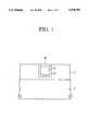
The integrated circuit device according to a first embodiment of the present invention will be explained with reference to FIG. 1.
The integrated circuit device according to the first embodiment is formed on asubstrate 10. In the first embodiment, thesubstrate 10 includes semiconductor substrates, such as silicon substrates, for semiconductor devices to be formed on, insulating substrates, such as ceramic substrates, for bearing wiring layers, and others. In multi-layer wirings thesubstrate 10 even includes substrates for bearing wiring layers, such as inter-insulating films of multi-layer wiring.
Aninsulating layer 12, as of SiO2 or others, is formed on thesubstrate 10. Abarrier layer 14 of, e.g., TiN is formed on the inside surface of an opening formed in theinsulating layer 12. Awiring layer 16 of copper is formed on thebarrier layer 14. Abarrier layer 18 of, e.g., TiN or others is formed on thecopper wiring layer 16.
Thus according to this embodiment, thecopper wiring layer 16 formed in the insulatinglayer 12 is all surrounded by thebarrier layers
The process for fabricating the integrated circuit device of FIG. 1 will be explained with reference to FIGS. 2A to 2E.
First, theinsulating film 12 is formed on thesubstrate 10 of, e.g., SiO2. Then, theopening 13 for the copper wiring layer to be formed in is formed by the usual lithography (FIG. 2A).
Subsequently TiN is deposited by sputtering on the entire surface of the insulatinglayer 12 including the inside surface of theopening 13 to form the barrier layer 14 (FIG. 2B).
Then copper is deposited by CVD on thebarrier layer 14 to form thewiring layer 16 which completely buries the opening 13 (FIG. 2B):
In the CVD for forming the copper wiring layer (CVD-Cu layer) 16, the source gas is Cu(HFA)tmvs [Cu(I)-hexafluoroacetylacetonato-trimethylvinylsilyl], the substrate temperature is 200 ° C., and the growth pressure is 1 Torr.
Then, thecopper wiring layer 16 is buff-abraded with a mixed aqueous solution (5%) of potassium iodide (KI) and iodine (I2) and an abrasive (trademark "Balkalox" 0.1 CR (0.1 μm-particle size)). The parts of thecopper wiring layers 16 and thebarrier layer 14 on theinsulating layer 16 are removed, and the buff-abrasion is set on until the upper surface of thecopper wiring layer 16 becomes lower than the upper surface of theinsulating layer 12, and thecopper wiring layer 16 is surrounded on the three sides by the barrier layer 14 (FIG. 2C). The buff-abrasion may be conducted with an aqueous solution (10-30%) of potassium chloride (KCl) and an abrasive agent.
Then, TiN is again deposited by sputtering on the entire surface of theinsulating layer 12 including thecopper wiring layer 16 lower than the upper surface of theinsulating layer 12 to form the barrier layer 18 (FIG. 2D).
Subsequently the upper surface of thebarrier layer 18 is abraded for planarization with a neutral or an alkaline abrasive liquid containing no acid by a hard abrasive cloth so that the upper surface of the insulatinglayer 12 and that of thebarrier layer 18 agree with each other (FIG. 2E).
Resultantly, thecopper wiring layer 16 is covered on the upper surface with thebarrier layer 18 and on the side surfaces and the bottom surface with thebarrier layer 14. Thus thecopper wiring layer 16 is surrounded on the four sides by the TiN barrier layers 14, 16.
Continuously another wiring layer can be formed on the insulatinglayer 12 and thecopper wiring layer 16 planarized with each other.
Thus according to the first embodiment, the copper wiring layer can be formed without conventionally etching a copper layer to leave a wiring layer. Furthermore, because of the copper wiring layer surrounded by the barrier layers, oxidation and diffusion of the copper can be precluded, and the surface of the copper wiring layer can be planarized.
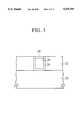
The integrated circuit device according to a second embodiment of the present invention will be explained with reference to FIG. 3.
The integrated circuit device according to the second embodiment is formed on asubstrate 20. In the second embodiment, thesubstrate 20 includes semiconductor substrates, such as silicon substrates, for semiconductor devices to be formed on, insulating substrates, such as ceramic substrates, for bearing wiring layers, and others. In multi-layer wirings thesubstrate 20 even includes lower wiring layers which are formed below the substrate.
An insulatinglayer 22, as of SiO2 or others, is formed on thesubstrate 20. Abarrier layer 24 of, e.g., TiN is formed on the inside surface of a contact hole formed in the insulatinglayer 22. Acontact layer 26 of copper is formed on thebarrier layer 24. Abarrier layer 28 of, e.g., TiN or others is formed on thecopper contact layer 26.
Thus according to this embodiment, thecopper contact layer 26 formed in the insulatinglayer 22 is all surrounded by the barrier layers 24, 28 and contacted with thesubstrate 20, and has the surface planarized.
The process for fabricating the integrated circuit device of FIG. 3 will be explained with reference to FIGS. 4A to 4E.
First, the insulatingfilm 22 is formed on thesubstrate 20 of, e.g., SiO2. Then, thecontact hole 23 for the copper contact layer to be formed in is formed in the insulatinglayer 22 by the usual lithography to expose the surface of the substrate 20 (FIG. 4A).
Subsequently TiN is deposited by sputtering on the entire surface of the insulatinglayer 22 including the inside surface of thecontact hole 23 to form the barrier layer 24 (FIG. 4B).
Then copper is deposited on thebarrier layer 24 by CVD to form thecontact layer 26 which completely buries the contact hole 23 (FIG. 4B).
Then, thecopper contact layer 26 is buff-abraded with a mixed solution (5%) of potassium iodide (KI), iodine (I2) and diluted nitric acid, and an abrasive. The parts of thecopper contact layer 26 and thebarrier layer 24 on the insulatinglayer 22 are removed, and the buff-abrasion is set on until the upper surface of thecopper contact layer 26 becomes lower than the upper surface of the insulatinglayer 22, and thecopper contact layer 26 is surrounded on the three sides by the barrier layer 24 (FIG. 4C).
Then, TiN is again deposited by sputtering on the entire surface of the insulatinglayer 22 including thecopper contact layer 26 lower than the upper surface of the insulatinglayer 22 to form the barrier layer 28 (FIG. 4D).
Subsequently the upper surface of thebarrier layer 28 is abraded for planarization with a neutral or an alkaline abrasive liquid containing no acid by a hard abrasive cloth so that the upper surface of the insulatinglayer 22 and that of thebarrier layer 18 agree with each other (FIG. 4E).
Resultantly, thecopper contact layer 26 is covered on the upper surface with thebarrier layer 28 and on the side surfaces and the bottom surface with thebarrier layer 24. Thus thecopper contact layer 26 is surrounded on the four sides by the TiN barrier layers 24, 26.
Continuously another copper contact layer can be formed on the insulatinglayer 22 and thecopper contact layer 26 planarized with each other.
Thus according to the second embodiment, the copper contact layer can be formed without conventionally etching a copper layer to leave a contact layer. Furthermore, because of the copper contact layer surrounded by the barrier layers, oxidation and diffusion of the copper can be precluded, and contact layers of high electromigration resistances and low resistances can be formed.
Furthermore, even though the contact layer is formed of copper, its surface can be planarized. Accordingly wiring layers formed on copper contact layers, and the substrate can be electrically connected.
The integrated circuit device according to a third embodiment of the present invention will be explained with reference to FIG. 3.
The third embodiment uses as an insulating layer an insulating material, such as silicon nitride (SiN), polyimide or others. In the first embodiment described above, the copper wiring layer is all surrounded by the barrier layers of TiN, but in the case that the insulating layer is formed of an insulating material containing substantially no oxygen, such as silicon nitride, polyimide or others, it is not necessary to form the barrier layers on the bottom surface and the side surfaces of the copper wiring layer because the copper wiring layer is not oxidized by the insulating layer.
The integrated circuit device according to the third embodiment is formed on asubstrate 30. In the third embodiment, thesubstrate 30 includes semiconductor substrates, such as silicon substrates, for semiconductor devices to be formed on, insulating substrates, such as ceramic substrates, for bearing wiring layers, and others. In multi-layer wirings thesubstrate 10 even includes substrates for bearing wiring layers, such as inter-insulating films of multi-layer wiring.
An insulatinglayer 32 of an insulating material containing substantially no oxygen, such as silicon nitride, polyimide or others, is formed on thesubstrate 30. Awiring layer 36 of copper is formed in an opening formed in the insulatinglayer 32, and abarrier layer 38 of TiN or others is formed on thecopper wiring layer 36.
Thus according to the third embodiment, the upper surface of thecopper wiring layer 36 formed in the insulatinglayer 32 is covered with thebarrier layer 38, and its surface is planarized.
The process for fabricating the integrated circuit device of FIG. 5 will be explained with reference to FIGS. 6A to 6E.
First, the insulatinglayer 32 of silicon nitride, polyimide or others is deposited on thesubstrate 30. Then anopening 32 for the copper wiring layer to be formed in is formed in the insulatinglayer 32 by the usual photolithography (FIG. 6A).
Then copper is deposited on the entire surface of the insulatinglayer 32 including the inside surface of theopening 33 by CVD to form thecopper wiring layer 36 which completely buries the opening 33 (FIG. 6B).
Next, thecopper wiring layer 36 is buff-abraded with a mixed aqueous solution (5%) of potassium iodine (KI) and iodine (I2), and an abrasive agent. The part of thecopper wiring layer 36 on the insulatinglayer 32 is removed, and the buff-abrasion is set On until the upper surface of thecopper wiring layer 36 becomes lower than the upper surface of the insulating layer 32 (FIG. 6C).
Then, TiN is deposited by CVD on the entire surface of the insulatinglayer 32 to form the barrier layer 38 (FIG. 6D).
Subsequently the upper surface of thebarrier layer 38 is abraded for planarization with a neutral or an alkaline abrasive liquid containing no acid and a hard abrasive cloth so that the upper surface of the insulatinglayer 32 and that of the barrier 88 agree with each other (FIG. 6E).
Resultantly thecopper wiring layer 36 is covered on the upper surface with thebarrier layer 38, and on the bottom and the side surfaces with the insulatinglayer 32 of an insulating material, such as silicon nitride, polyimide or others containing substantially no oxygen.
Continuously another wiring layer can be formed on the insulatinglayer 32 and thecopper wiring layer 36 planarized with each other.
Thus according to the third embodiment, the copper wiring layer can be formed without conventionally etching a copper layer to leave a wiring layer. Furthermore, because of the copper wiring layer surrounded by the layers of materials containing substantially no oxygen, oxidation and diffusion of the copper can be precluded, and wiring layers of high electromigration resistances and low resistances can be formed. Furthermore, even though the wiring layer is formed of copper, its surface can be planarized.
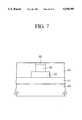
The integrated circuit device according to a fourth embodiment of the present invention will be explained with reference to FIG. 7.
The integrated circuit device according to the fourth embodiment is formed on asubstrate 40.
In this embodiment thesubstrate 40 includes semiconductor substrates, such as silicon substrates, etc. for semiconductor devices to be formed on, and insulating substrates, etc., such as ceramic substrates bearing wiring layers.
Alower wiring layer 42 of aluminium is formed on thesubstrate 40 through an insulatinglayer 42 of, e.g., SiO2. An insulatinglayer 44 of an insulating material containing substantially no oxygen, such as silicon nitride, polyimide or others is formed on the wiring layer 52. A contact layer ofcopper 46 is burled in a contact hole formed in the insulatinglayer 44, and tabarrier layer 48 of, e.g., TiN is formed on thecopper contact layer 46.
Thus, according to the fourth embodiment, thecopper contact layer 46 formed in the insulatinglayer 44 is coated on the upper surface with thebarrier layer 48, on the side surfaces with the insulatinglayer 44 of an insulating material containing substantially no oxygen. Thecopper contact layer 46 is contacted with thesubstrate 40, and has the upper surface planarized.
The process for fabricating the integrated circuit device of FIG. 7 will be explained with reference to FIGS. 8A to 8E.
First, an insulatinglayer 41 of, e.g., SiO2 is formed on asubstrate 40. Then awiring layer 42 of aluminium is deposited on the insulatinglayer 41, and is patterned as alower wiring layer 42. Subsequently an insulating material containing substantially no oxygen, such as silicon nitride, polyimide or others is deposited on the entire surface to form the insulatinglayer 44. Then acontact hole 45 for the copper contact layer to be formed in is formed by the usual photolithography to expose the surface of the lower wiring layer 42 (FIG. 8A).
Then copper is deposited on the entire surface of the insulatinglayer 44 including the exposed surface of thewiring layer 42 and the inside surface of thecontact hole 45 to form thecopper contact layer 46 which completely buries the contact hole 45 (FIG. 8B).
Then, thecopper contact layer 46 is buff-abraded with a mixed solution (5%) of potassium iodine (KI), iodine (I2) and diluted nitric acid, and an abrasive agent. The part of thecopper contact layer 46 on the insulatinglayer 44 is removed. The buff-abrasion is set on until the upper surface of thecopper contact layer 46 becomes lower than that of the insulatinglayer 44, and thecopper contact layer 46 is formed (FIG. 8C).
Next, Tin is deposited by sputtering on the entire surface of the insulatinglayer 44 including thecopper contact layer 46 lower than the upper surface of the insulatinglayer 44 to form the barrier layer 48 (FIG. 8D).
Then, the upper surface of thebarrier layer 48 is abraded for planarization with a neutral or an alkaline abrasive liquid containing substantially no oxygen and a hard abrasive cloth so that the upper surface of the insulatinglayer 44 and that of thebarrier layer 48 agree with each other (FIG. 8E).
Resultantly thecopper contact layer 46 has the upper surface coated with thebarrier layer 48.
Continuously another wiring layer can be formed on the insulatinglayer 44 and thecopper contact layer 46 planarized with each other.
Thus according to the fourth embodiment, the copper wiring layer can be formed without conventionally etching a copper layer to leave a wiring layer. Furthermore, because of the copper wiring layer surrounded by the layers of materials containing substantially no oxygen, oxidation and diffusion of the copper can be precluded, and wiring layers of high electromigration resistances and low resistances can be formed. Furthermore, even though the wiring layer is formed of copper, its surface can be planarized.
Claims (16)
1. A process for fabricating an integrated circuit device comprising:
a first step of forming an opening in an insulating layer formed on a substrate;
a second step of depositing a copper layer on the substrate including the opening;
a third step of abrading the copper layer to remove the copper layer deposited on the insulating layer, while part of the copper layer deposited in the opening is removed until the upper surface of the copper layer deposited in the opening becomes lower then the upper surface of the insulating layer;
a fourth step of depositing a barrier layer on the substrate including the copper layer in the opening; and
a fifth step of abrading the barrier layer to remove part of the barrier layer on the insulating layer while part of the barrier layer on the copper layer in the opening is left, so as to planarize the surface.
2. A process for fabricating an integrated circuit device according to claim 1,
wherein the opening formed in the insulating layer is a grooved opening, and the copper layer deposited in the grooved opening is a wiring layer.
3. A process for fabricating an integrated circuit device according to claim 1,
wherein the opening formed in the insulating layer is a contact hole which reaches the substrate, and the copper layer deposited in the contact hole forms a contact with the substrate.
4. A process for fabricating an integrated circuit device according to claim 1,
wherein the insulating layer is formed of an insulating material containing no oxygen.
5. A process for fabricating an integrated circuit device according to claim 4,
wherein the insulating material containing no oxygen is silicon nitride or polyimide.
6. A process for fabricating an integrated circuit device according to claim 1,
wherein the barrier layer is formed of TiN.
7. A process for fabricating an integrated circuit device according to claim 1,
wherein the third is for buff-abrading with an aqueous solution of potassium iodine or potassium chloride, and an abrasive agent.
8. The process for fabricating an integrated circuit device according to claim 1,
wherein said fifth step of abrading the barrier layer includes abrading with a neutral abrasive liquid.
9. The process for fabricating an integrated circuit device according to claim 1,
wherein said fifth step of abrading the barrier layer includes abrading with a hard abrasive cloth.
10. A process for fabricating an integrated circuit device comprising:
a first step of forming an opening in an insulating layer formed on a substrate;
a second step of depositing a first barrier layer on the substrate including the opening;
a third step of depositing a copper layer on the first barrier layer;
a fourth step of abrading the copper layer to remove the copper layer and the first barrier layer deposited on the insulating layer, while part of the copper layer deposited in the opening is removed until the upper surface of the copper layer deposited in the opening becomes lower than the upper surface of the insulating layer;
a fifth step of depositing a second barrier layer on the substrate including the copper layer in the opening; and
a sixth step of abrading the second barrier layer to remove the second barrier layer on the insulating layer while leaving part of the second barrier layer on the copper layer in the opening, so as to planarize the surface.
11. A process for fabricating an integrated circuit device according to claim 10,
wherein the opening formed in the insulating layer is a grooved opening, and the copper layer deposited in the grooved opening is a wiring layer.
12. A process for fabricating an integrated circuit device according to claim 10,
wherein the opening formed in the insulating layer is a contact hole which reaches the substrate, and the copper layer deposited in the contact hole forms a contact with the substrate.
13. A process for fabricating an integrated circuit device according to claim 10,
wherein the insulating layer is formed of an insulating material containing oxygen.
14. A process for fabricating an integrated circuit device according to claim 13,
wherein the insulating material containing oxygen is silicon oxide.
15. A process for fabricating an integrated circuit device according to claim 10,
wherein the barrier layer is formed of TiN.
16. A process for fabricating an integrated circuit device according to claim 10,
wherein the fourth step is for buff-abrading with an aqueous solution of potassium iodine or potassium chloride, and an abrasive agent.
Priority Applications (1)
| Application Number | Priority Date | Filing Date | Title |
|---|---|---|---|
| US08/400,504US5470789A (en) | 1993-03-19 | 1995-03-07 | Process for fabricating integrated circuit devices |
Applications Claiming Priority (4)
| Application Number | Priority Date | Filing Date | Title |
|---|---|---|---|
| JP5-059889 | 1993-03-19 | ||
| JP05988993AJP3326698B2 (en) | 1993-03-19 | 1993-03-19 | Manufacturing method of integrated circuit device |
| US20498694A | 1994-03-02 | 1994-03-02 | |
| US08/400,504US5470789A (en) | 1993-03-19 | 1995-03-07 | Process for fabricating integrated circuit devices |
Related Parent Applications (1)
| Application Number | Title | Priority Date | Filing Date |
|---|---|---|---|
| US20498694AContinuation | 1993-03-19 | 1994-03-02 |
Publications (1)
| Publication Number | Publication Date |
|---|---|
| US5470789Atrue US5470789A (en) | 1995-11-28 |
Family
ID=13126145
Family Applications (1)
| Application Number | Title | Priority Date | Filing Date |
|---|---|---|---|
| US08/400,504Expired - LifetimeUS5470789A (en) | 1993-03-19 | 1995-03-07 | Process for fabricating integrated circuit devices |
Country Status (2)
| Country | Link |
|---|---|
| US (1) | US5470789A (en) |
| JP (1) | JP3326698B2 (en) |
Cited By (59)
| Publication number | Priority date | Publication date | Assignee | Title |
|---|---|---|---|---|
| US5547901A (en)* | 1994-05-24 | 1996-08-20 | Lg Semicon Co., Ltd. | Method for forming a copper metal wiring with aluminum containing oxidation barrier |
| US5591671A (en)* | 1994-01-18 | 1997-01-07 | Samsung Electronics Co., Ltd. | Method for interconnecting layers in semiconductor device |
| US5744376A (en)* | 1996-04-08 | 1998-04-28 | Chartered Semiconductor Manufacturing Pte, Ltd | Method of manufacturing copper interconnect with top barrier layer |
| US5747379A (en)* | 1996-01-11 | 1998-05-05 | Taiwan Semiconductor Manufacturing Company, Ltd. | Method of fabricating seamless tungsten plug employing tungsten redeposition and etch back |
| US5770519A (en)* | 1995-06-05 | 1998-06-23 | Advanced Micro Devices, Inc. | Copper reservoir for reducing electromigration effects associated with a conductive via in a semiconductor device |
| US5795796A (en)* | 1995-12-26 | 1998-08-18 | Lg Semicon Co., Ltd. | Method of fabricating metal line structure |
| EP0913863A3 (en)* | 1997-10-31 | 1999-05-19 | Nec Corporation | Method of manufacturing semiconductor device with copper wiring film |
| US6010960A (en)* | 1997-10-29 | 2000-01-04 | Advanced Micro Devices, Inc. | Method and system for providing an interconnect having reduced failure rates due to voids |
| US6046108A (en)* | 1999-06-25 | 2000-04-04 | Taiwan Semiconductor Manufacturing Company | Method for selective growth of Cu3 Ge or Cu5 Si for passivation of damascene copper structures and device manufactured thereby |
| US6066560A (en)* | 1998-05-05 | 2000-05-23 | Lsi Logic Corporation | Non-linear circuit elements on integrated circuits |
| US6100195A (en)* | 1998-12-28 | 2000-08-08 | Chartered Semiconductor Manu. Ltd. | Passivation of copper interconnect surfaces with a passivating metal layer |
| US6100196A (en)* | 1996-04-08 | 2000-08-08 | Chartered Semiconductor Manufacturing Ltd. | Method of making a copper interconnect with top barrier layer |
| US6114243A (en)* | 1999-11-15 | 2000-09-05 | Chartered Semiconductor Manufacturing Ltd | Method to avoid copper contamination on the sidewall of a via or a dual damascene structure |
| US6114238A (en)* | 1998-01-26 | 2000-09-05 | United Silicon Incorporated | Self-aligned metal nitride for copper passivation |
| US6130161A (en)* | 1997-05-30 | 2000-10-10 | International Business Machines Corporation | Method of forming copper interconnections with enhanced electromigration resistance and reduced defect sensitivity |
| US6171957B1 (en) | 1997-07-16 | 2001-01-09 | Mitsubishi Denki Kabushiki Kaisha | Manufacturing method of semiconductor device having high pressure reflow process |
| US6208016B1 (en) | 1998-09-10 | 2001-03-27 | Micron Technology, Inc. | Forming submicron integrated-circuit wiring from gold, silver, copper and other metals |
| US6211073B1 (en) | 1998-02-27 | 2001-04-03 | Micron Technology, Inc. | Methods for making copper and other metal interconnections in integrated circuits |
| US6218734B1 (en)* | 1996-09-20 | 2001-04-17 | Sharp Laboratories Of America, Inc. | Copper adhered to a diffusion barrier surface |
| US6251774B1 (en) | 1998-11-10 | 2001-06-26 | Mitsubishi Denki Kabushiki Kaisha | Method of manufacturing a semiconductor device |
| US6274499B1 (en) | 1999-11-19 | 2001-08-14 | Chartered Semiconductor Manufacturing Ltd. | Method to avoid copper contamination during copper etching and CMP |
| US6284656B1 (en) | 1998-08-04 | 2001-09-04 | Micron Technology, Inc. | Copper metallurgy in integrated circuits |
| US6294463B1 (en)* | 2000-09-13 | 2001-09-25 | Vanguard International Semiconductor Corp. | Method for manufacturing diffusion barrier layer |
| US6333248B1 (en)* | 1999-11-11 | 2001-12-25 | Nec Corporation | Method of fabricating a semiconductor device |
| US6339258B1 (en) | 1999-07-02 | 2002-01-15 | International Business Machines Corporation | Low resistivity tantalum |
| US6342444B1 (en) | 1999-03-11 | 2002-01-29 | Kabushiki Kaisha Toshiba | Method of forming diffusion barrier for copper interconnects |
| US6348734B1 (en)* | 1999-04-21 | 2002-02-19 | National Semiconductor Corporation | Self-aligned copper interconnect architecture with enhanced copper diffusion barrier |
| US6359328B1 (en) | 1998-12-31 | 2002-03-19 | Intel Corporation | Methods for making interconnects and diffusion barriers in integrated circuits |
| US6433429B1 (en) | 1999-09-01 | 2002-08-13 | International Business Machines Corporation | Copper conductive line with redundant liner and method of making |
| US20020127845A1 (en)* | 1999-03-01 | 2002-09-12 | Paul A. Farrar | Conductive structures in integrated circuits |
| DE19920970C2 (en)* | 1998-05-07 | 2002-10-24 | Samsung Electronics Co Ltd | Method for forming contact paths and simultaneously planarizing a substrate surface in integrated circuits |
| US6537912B1 (en) | 2000-08-25 | 2003-03-25 | Micron Technology Inc. | Method of forming an encapsulated conductive pillar |
| US6579785B2 (en) | 2000-01-25 | 2003-06-17 | Kabushiki Kaisha Toshiba | Method of making multi-level wiring in a semiconductor device |
| WO2003021661A3 (en)* | 2001-08-29 | 2003-07-24 | Motorola Inc | Process for making a mim capacitor |
| US6611060B1 (en) | 1999-10-04 | 2003-08-26 | Kabushiki Kaisha Toshiba | Semiconductor device having a damascene type wiring layer |
| US20030228749A1 (en)* | 2002-06-06 | 2003-12-11 | Nishant Sinha | Plating metal caps on conductive interconnect for wirebonding |
| US6696761B2 (en) | 1998-11-20 | 2004-02-24 | Chartered Semiconductor Manufacturing Ltd. | Method to encapsulate copper plug for interconnect metallization |
| US6743716B2 (en) | 2000-01-18 | 2004-06-01 | Micron Technology, Inc. | Structures and methods to enhance copper metallization |
| US6750541B2 (en)* | 2001-04-27 | 2004-06-15 | Fujitsu Limited | Semiconductor device |
| US6756298B2 (en) | 2000-01-18 | 2004-06-29 | Micron Technology, Inc. | Methods and apparatus for making integrated-circuit wiring from copper, silver, gold, and other metals |
| US6777807B1 (en)* | 2003-05-29 | 2004-08-17 | Lsi Logic Corporation | Interconnect integration |
| US6995470B2 (en) | 2000-05-31 | 2006-02-07 | Micron Technology, Inc. | Multilevel copper interconnects with low-k dielectrics and air gaps |
| US20060063365A1 (en)* | 2004-09-23 | 2006-03-23 | Wang Chung Y | Aluminum cap for reducing scratch and wire-bond bridging of bond pads |
| US20060115976A1 (en)* | 2004-11-29 | 2006-06-01 | Chan Elvis M | Metal capping of damascene structures to improve reliability using hyper selective chemical-mechanical deposition |
| US7067421B2 (en) | 2000-05-31 | 2006-06-27 | Micron Technology, Inc. | Multilevel copper interconnect with double passivation |
| US7105914B2 (en) | 2000-01-18 | 2006-09-12 | Micron Technology, Inc. | Integrated circuit and seed layers |
| US20060286720A1 (en)* | 2005-06-17 | 2006-12-21 | Matsushita Electric Industrial Co., Ltd. | Method for fabricating nonvolatile semiconductor memory device |
| US7220665B2 (en) | 2003-08-05 | 2007-05-22 | Micron Technology, Inc. | H2 plasma treatment |
| US7253521B2 (en) | 2000-01-18 | 2007-08-07 | Micron Technology, Inc. | Methods for making integrated-circuit wiring from copper, silver, gold, and other metals |
| US7262505B2 (en) | 2000-01-18 | 2007-08-28 | Micron Technology, Inc. | Selective electroless-plated copper metallization |
| US20070278695A1 (en)* | 1998-08-28 | 2007-12-06 | Micron Technology, Inc. | Interconnect structures |
| US20070277736A1 (en)* | 2006-05-31 | 2007-12-06 | Mec Company Ltd. | Method for manufacturing substrate, and vapor deposition apparatus used for the same |
| US20080242080A1 (en)* | 2007-03-30 | 2008-10-02 | Sandisk 3D Llc | Method for implementing diffusion barrier in 3D memory |
| US20080237862A1 (en)* | 2007-03-30 | 2008-10-02 | Sandisk 3D Llc | Implementation of diffusion barrier in 3D memory |
| US20090289368A1 (en)* | 2006-11-15 | 2009-11-26 | International Business Machines Corporation | Interconnect structure having enhanced electromigration reliabilty and a method of fabricating same |
| US7863654B2 (en) | 1998-12-21 | 2011-01-04 | Megica Corporation | Top layers of metal for high performance IC's |
| US20130256899A1 (en)* | 2011-11-04 | 2013-10-03 | Boyan Boyanov | Methods and apparatuses to form self-aligned caps |
| US8722530B2 (en) | 2011-07-28 | 2014-05-13 | Freescale Semiconductor, Inc. | Method of making a die with recessed aluminum die pads |
| US20230343697A1 (en)* | 2022-04-20 | 2023-10-26 | Samsung Electronics Co., Ltd. | Semiconductor device including spacer via structure and method of manufacturing the same |
Families Citing this family (15)
| Publication number | Priority date | Publication date | Assignee | Title |
|---|---|---|---|---|
| JPH08236621A (en)* | 1995-02-28 | 1996-09-13 | Nec Corp | Fabrication of semiconductor device |
| JP3607424B2 (en)* | 1996-07-12 | 2005-01-05 | 株式会社東芝 | Semiconductor device and manufacturing method thereof |
| KR100325383B1 (en) | 1996-07-12 | 2002-04-17 | 니시무로 타이죠 | Semiconductor device and method of manufacturing the same |
| JP3645682B2 (en)* | 1997-03-18 | 2005-05-11 | 三菱電機株式会社 | CVD equipment for Cu film formation |
| KR19990003485A (en)* | 1997-06-25 | 1999-01-15 | 김영환 | Metal wiring formation method of semiconductor device |
| KR19990003484A (en)* | 1997-06-25 | 1999-01-15 | 김영환 | Metal wiring formation method of semiconductor device |
| KR100274346B1 (en)* | 1997-06-30 | 2001-01-15 | 김영환 | Method of forming a metal wiring in a semiconductor device |
| KR100471404B1 (en)* | 1998-10-28 | 2005-05-27 | 주식회사 하이닉스반도체 | Method for forming metal wiring of semiconductor device using chemical mechanical polishing process |
| JP3708732B2 (en)* | 1998-12-25 | 2005-10-19 | Necエレクトロニクス株式会社 | Manufacturing method of semiconductor device |
| KR100309474B1 (en)* | 1999-11-05 | 2001-11-02 | 박종섭 | Metal line forming method |
| JP4064595B2 (en)* | 2000-03-28 | 2008-03-19 | 株式会社東芝 | Manufacturing method of semiconductor device |
| JP3979791B2 (en)* | 2000-03-08 | 2007-09-19 | 株式会社ルネサステクノロジ | Semiconductor device and manufacturing method thereof |
| JP4644924B2 (en)* | 2000-10-12 | 2011-03-09 | ソニー株式会社 | Semiconductor device and manufacturing method thereof |
| KR20020034373A (en)* | 2000-11-01 | 2002-05-09 | 박종섭 | Method for forming metal wire of semiconductor device |
| JP4272168B2 (en) | 2003-03-28 | 2009-06-03 | 富士通マイクロエレクトロニクス株式会社 | Semiconductor device and semiconductor integrated circuit device |
Citations (8)
| Publication number | Priority date | Publication date | Assignee | Title |
|---|---|---|---|---|
| US5008216A (en)* | 1988-10-03 | 1991-04-16 | International Business Machines Corporation | Process for improved contact stud structure for semiconductor devices |
| US5071789A (en)* | 1985-08-02 | 1991-12-10 | Kabushiki Kaisha Toshiba | Method for forming a metal electrical connector to a surface of a semiconductor device adjacent a sidewall of insulation material with metal creep-up extending up that sidewall, and related device |
| US5084413A (en)* | 1986-04-15 | 1992-01-28 | Matsushita Electric Industrial Co., Ltd. | Method for filling contact hole |
| US5130274A (en)* | 1991-04-05 | 1992-07-14 | International Business Machines Corporation | Copper alloy metallurgies for VLSI interconnection structures |
| US5164330A (en)* | 1991-04-17 | 1992-11-17 | Intel Corporation | Etchback process for tungsten utilizing a NF3/AR chemistry |
| US5219789A (en)* | 1991-04-19 | 1993-06-15 | Sharp Kabushiki Kaisha | Method for forming contact portion of semiconductor device |
| US5254498A (en)* | 1991-05-23 | 1993-10-19 | Sony Corporation | Method for forming barrier metal structure |
| US5262354A (en)* | 1992-02-26 | 1993-11-16 | International Business Machines Corporation | Refractory metal capped low resistivity metal conductor lines and vias |
- 1993
- 1993-03-19JPJP05988993Apatent/JP3326698B2/ennot_activeExpired - Lifetime
- 1995
- 1995-03-07USUS08/400,504patent/US5470789A/ennot_activeExpired - Lifetime
Patent Citations (8)
| Publication number | Priority date | Publication date | Assignee | Title |
|---|---|---|---|---|
| US5071789A (en)* | 1985-08-02 | 1991-12-10 | Kabushiki Kaisha Toshiba | Method for forming a metal electrical connector to a surface of a semiconductor device adjacent a sidewall of insulation material with metal creep-up extending up that sidewall, and related device |
| US5084413A (en)* | 1986-04-15 | 1992-01-28 | Matsushita Electric Industrial Co., Ltd. | Method for filling contact hole |
| US5008216A (en)* | 1988-10-03 | 1991-04-16 | International Business Machines Corporation | Process for improved contact stud structure for semiconductor devices |
| US5130274A (en)* | 1991-04-05 | 1992-07-14 | International Business Machines Corporation | Copper alloy metallurgies for VLSI interconnection structures |
| US5164330A (en)* | 1991-04-17 | 1992-11-17 | Intel Corporation | Etchback process for tungsten utilizing a NF3/AR chemistry |
| US5219789A (en)* | 1991-04-19 | 1993-06-15 | Sharp Kabushiki Kaisha | Method for forming contact portion of semiconductor device |
| US5254498A (en)* | 1991-05-23 | 1993-10-19 | Sony Corporation | Method for forming barrier metal structure |
| US5262354A (en)* | 1992-02-26 | 1993-11-16 | International Business Machines Corporation | Refractory metal capped low resistivity metal conductor lines and vias |
Cited By (115)
| Publication number | Priority date | Publication date | Assignee | Title |
|---|---|---|---|---|
| US5591671A (en)* | 1994-01-18 | 1997-01-07 | Samsung Electronics Co., Ltd. | Method for interconnecting layers in semiconductor device |
| US5547901A (en)* | 1994-05-24 | 1996-08-20 | Lg Semicon Co., Ltd. | Method for forming a copper metal wiring with aluminum containing oxidation barrier |
| US5770519A (en)* | 1995-06-05 | 1998-06-23 | Advanced Micro Devices, Inc. | Copper reservoir for reducing electromigration effects associated with a conductive via in a semiconductor device |
| US5795796A (en)* | 1995-12-26 | 1998-08-18 | Lg Semicon Co., Ltd. | Method of fabricating metal line structure |
| US5747379A (en)* | 1996-01-11 | 1998-05-05 | Taiwan Semiconductor Manufacturing Company, Ltd. | Method of fabricating seamless tungsten plug employing tungsten redeposition and etch back |
| US5744376A (en)* | 1996-04-08 | 1998-04-28 | Chartered Semiconductor Manufacturing Pte, Ltd | Method of manufacturing copper interconnect with top barrier layer |
| US6100196A (en)* | 1996-04-08 | 2000-08-08 | Chartered Semiconductor Manufacturing Ltd. | Method of making a copper interconnect with top barrier layer |
| US6218734B1 (en)* | 1996-09-20 | 2001-04-17 | Sharp Laboratories Of America, Inc. | Copper adhered to a diffusion barrier surface |
| US6287954B1 (en) | 1997-05-30 | 2001-09-11 | International Business Machines Corporation | Method of forming copper interconnections with enhanced electromigration resistance and reduced defect sensitivity |
| US6348731B1 (en) | 1997-05-30 | 2002-02-19 | International Business Machines Corporation | Copper interconnections with enhanced electromigration resistance and reduced defect sensitivity and method of forming same |
| US6130161A (en)* | 1997-05-30 | 2000-10-10 | International Business Machines Corporation | Method of forming copper interconnections with enhanced electromigration resistance and reduced defect sensitivity |
| US6171957B1 (en) | 1997-07-16 | 2001-01-09 | Mitsubishi Denki Kabushiki Kaisha | Manufacturing method of semiconductor device having high pressure reflow process |
| US6010960A (en)* | 1997-10-29 | 2000-01-04 | Advanced Micro Devices, Inc. | Method and system for providing an interconnect having reduced failure rates due to voids |
| EP0913863A3 (en)* | 1997-10-31 | 1999-05-19 | Nec Corporation | Method of manufacturing semiconductor device with copper wiring film |
| US6114238A (en)* | 1998-01-26 | 2000-09-05 | United Silicon Incorporated | Self-aligned metal nitride for copper passivation |
| US6211073B1 (en) | 1998-02-27 | 2001-04-03 | Micron Technology, Inc. | Methods for making copper and other metal interconnections in integrated circuits |
| US6984891B2 (en) | 1998-02-27 | 2006-01-10 | Micron Technology, Inc. | Methods for making copper and other metal interconnections in integrated circuits |
| US6066560A (en)* | 1998-05-05 | 2000-05-23 | Lsi Logic Corporation | Non-linear circuit elements on integrated circuits |
| US6228767B1 (en)* | 1998-05-05 | 2001-05-08 | Lsi Logic Corporation | Non-linear circuit elements on integrated circuits |
| DE19920757B4 (en)* | 1998-05-05 | 2008-05-15 | Lsi Logic Corp., Fort Collins | A method of forming a non-linear switching element on an integrated circuit and electrical interconnect structure |
| DE19920970C2 (en)* | 1998-05-07 | 2002-10-24 | Samsung Electronics Co Ltd | Method for forming contact paths and simultaneously planarizing a substrate surface in integrated circuits |
| US6614099B2 (en) | 1998-08-04 | 2003-09-02 | Micron Technology, Inc. | Copper metallurgy in integrated circuits |
| US6284656B1 (en) | 1998-08-04 | 2001-09-04 | Micron Technology, Inc. | Copper metallurgy in integrated circuits |
| US7955976B2 (en) | 1998-08-28 | 2011-06-07 | Micron Technology, Inc. | Methods of forming semiconductor structures |
| US20070278695A1 (en)* | 1998-08-28 | 2007-12-06 | Micron Technology, Inc. | Interconnect structures |
| US20100087060A1 (en)* | 1998-08-28 | 2010-04-08 | Micron Technology, Inc. | Methods of forming semiconductor structures |
| US7659630B2 (en)* | 1998-08-28 | 2010-02-09 | Micron Technology, Inc. | Interconnect structures with interlayer dielectric |
| US6849927B2 (en) | 1998-09-10 | 2005-02-01 | Micron Technology, Inc. | Forming submicron integrated-circuit wiring from gold, silver, copper, and other metals |
| US6288442B1 (en) | 1998-09-10 | 2001-09-11 | Micron Technology, Inc. | Integrated circuit with oxidation-resistant polymeric layer |
| US20010010403A1 (en)* | 1998-09-10 | 2001-08-02 | Micron Technology, Inc. | Forming submicron integrated-circuit wiring from gold, silver, copper, and other metals |
| US6211049B1 (en) | 1998-09-10 | 2001-04-03 | Micron Technology, Inc. | Forming submicron integrated-circuit wiring from gold, silver, copper, and other metals |
| US6208016B1 (en) | 1998-09-10 | 2001-03-27 | Micron Technology, Inc. | Forming submicron integrated-circuit wiring from gold, silver, copper and other metals |
| US6552432B2 (en) | 1998-09-10 | 2003-04-22 | Micron Technology, Inc. | Mask on a polymer having an opening width less than that of the opening in the polymer |
| US6251774B1 (en) | 1998-11-10 | 2001-06-26 | Mitsubishi Denki Kabushiki Kaisha | Method of manufacturing a semiconductor device |
| US6696761B2 (en) | 1998-11-20 | 2004-02-24 | Chartered Semiconductor Manufacturing Ltd. | Method to encapsulate copper plug for interconnect metallization |
| US8415800B2 (en) | 1998-12-21 | 2013-04-09 | Megica Corporation | Top layers of metal for high performance IC's |
| US7863654B2 (en) | 1998-12-21 | 2011-01-04 | Megica Corporation | Top layers of metal for high performance IC's |
| US8531038B2 (en) | 1998-12-21 | 2013-09-10 | Megica Corporation | Top layers of metal for high performance IC's |
| US8471384B2 (en) | 1998-12-21 | 2013-06-25 | Megica Corporation | Top layers of metal for high performance IC's |
| US8022545B2 (en) | 1998-12-21 | 2011-09-20 | Megica Corporation | Top layers of metal for high performance IC's |
| US7884479B2 (en) | 1998-12-21 | 2011-02-08 | Megica Corporation | Top layers of metal for high performance IC's |
| US7999384B2 (en) | 1998-12-21 | 2011-08-16 | Megica Corporation | Top layers of metal for high performance IC's |
| US6468906B1 (en) | 1998-12-28 | 2002-10-22 | Chartered Semiconductor Manufacturing Ltd. | Passivation of copper interconnect surfaces with a passivating metal layer |
| US6100195A (en)* | 1998-12-28 | 2000-08-08 | Chartered Semiconductor Manu. Ltd. | Passivation of copper interconnect surfaces with a passivating metal layer |
| US20020094673A1 (en)* | 1998-12-31 | 2002-07-18 | Intel Corporation | Method for making interconnects and diffusion barriers in integrated circuits |
| US6359328B1 (en) | 1998-12-31 | 2002-03-19 | Intel Corporation | Methods for making interconnects and diffusion barriers in integrated circuits |
| US6933230B2 (en) | 1998-12-31 | 2005-08-23 | Intel Corporation | Method for making interconnects and diffusion barriers in integrated circuits |
| US20020127845A1 (en)* | 1999-03-01 | 2002-09-12 | Paul A. Farrar | Conductive structures in integrated circuits |
| US20050285272A1 (en)* | 1999-03-01 | 2005-12-29 | Micron Technology, Inc. | Conductive structures in integrated circuits |
| US6342444B1 (en) | 1999-03-11 | 2002-01-29 | Kabushiki Kaisha Toshiba | Method of forming diffusion barrier for copper interconnects |
| US6348734B1 (en)* | 1999-04-21 | 2002-02-19 | National Semiconductor Corporation | Self-aligned copper interconnect architecture with enhanced copper diffusion barrier |
| US6046108A (en)* | 1999-06-25 | 2000-04-04 | Taiwan Semiconductor Manufacturing Company | Method for selective growth of Cu3 Ge or Cu5 Si for passivation of damascene copper structures and device manufactured thereby |
| US6339258B1 (en) | 1999-07-02 | 2002-01-15 | International Business Machines Corporation | Low resistivity tantalum |
| US6433429B1 (en) | 1999-09-01 | 2002-08-13 | International Business Machines Corporation | Copper conductive line with redundant liner and method of making |
| US6897143B2 (en) | 1999-10-04 | 2005-05-24 | Kabushiki Kaisha Toshiba | Method of manufacturing semiconductor device including two-step polishing operation for cap metal |
| US20040005774A1 (en)* | 1999-10-04 | 2004-01-08 | Kabushiki Kaisha Toshiba | Method of manufacturing semiconductor device and semiconductor device |
| US6611060B1 (en) | 1999-10-04 | 2003-08-26 | Kabushiki Kaisha Toshiba | Semiconductor device having a damascene type wiring layer |
| US6333248B1 (en)* | 1999-11-11 | 2001-12-25 | Nec Corporation | Method of fabricating a semiconductor device |
| US6114243A (en)* | 1999-11-15 | 2000-09-05 | Chartered Semiconductor Manufacturing Ltd | Method to avoid copper contamination on the sidewall of a via or a dual damascene structure |
| EP1102315A3 (en)* | 1999-11-15 | 2003-09-24 | Chartered Semiconductor Manufacturing Pte Ltd. | A method to avoid copper contamination on the sidewall of a via or a dual damascene structure |
| US6274499B1 (en) | 1999-11-19 | 2001-08-14 | Chartered Semiconductor Manufacturing Ltd. | Method to avoid copper contamination during copper etching and CMP |
| US7402516B2 (en) | 2000-01-18 | 2008-07-22 | Micron Technology, Inc. | Method for making integrated circuits |
| US7262130B1 (en) | 2000-01-18 | 2007-08-28 | Micron Technology, Inc. | Methods for making integrated-circuit wiring from copper, silver, gold, and other metals |
| US8779596B2 (en) | 2000-01-18 | 2014-07-15 | Micron Technology, Inc. | Structures and methods to enhance copper metallization |
| US7670469B2 (en) | 2000-01-18 | 2010-03-02 | Micron Technology, Inc. | Methods and apparatus for making integrated-circuit wiring from copper, silver, gold, and other metals |
| US7535103B2 (en) | 2000-01-18 | 2009-05-19 | Micron Technology, Inc. | Structures and methods to enhance copper metallization |
| US7378737B2 (en) | 2000-01-18 | 2008-05-27 | Micron Technology, Inc. | Structures and methods to enhance copper metallization |
| US7105914B2 (en) | 2000-01-18 | 2006-09-12 | Micron Technology, Inc. | Integrated circuit and seed layers |
| US6756298B2 (en) | 2000-01-18 | 2004-06-29 | Micron Technology, Inc. | Methods and apparatus for making integrated-circuit wiring from copper, silver, gold, and other metals |
| US7745934B2 (en) | 2000-01-18 | 2010-06-29 | Micron Technology, Inc. | Integrated circuit and seed layers |
| US7253521B2 (en) | 2000-01-18 | 2007-08-07 | Micron Technology, Inc. | Methods for making integrated-circuit wiring from copper, silver, gold, and other metals |
| US7262505B2 (en) | 2000-01-18 | 2007-08-28 | Micron Technology, Inc. | Selective electroless-plated copper metallization |
| US6743716B2 (en) | 2000-01-18 | 2004-06-01 | Micron Technology, Inc. | Structures and methods to enhance copper metallization |
| US7285196B2 (en) | 2000-01-18 | 2007-10-23 | Micron Technology, Inc. | Methods and apparatus for making integrated-circuit wiring from copper, silver, gold, and other metals |
| US7301190B2 (en) | 2000-01-18 | 2007-11-27 | Micron Technology, Inc. | Structures and methods to enhance copper metallization |
| US7368378B2 (en) | 2000-01-18 | 2008-05-06 | Micron Technology, Inc. | Methods for making integrated-circuit wiring from copper, silver, gold, and other metals |
| US7394157B2 (en) | 2000-01-18 | 2008-07-01 | Micron Technology, Inc. | Integrated circuit and seed layers |
| US6579785B2 (en) | 2000-01-25 | 2003-06-17 | Kabushiki Kaisha Toshiba | Method of making multi-level wiring in a semiconductor device |
| US20030214010A1 (en)* | 2000-01-25 | 2003-11-20 | Kabushiki Kaisha Toshiba | Semiconductor device and method of manufacturing the same |
| US6995470B2 (en) | 2000-05-31 | 2006-02-07 | Micron Technology, Inc. | Multilevel copper interconnects with low-k dielectrics and air gaps |
| US7091611B2 (en) | 2000-05-31 | 2006-08-15 | Micron Technology, Inc. | Multilevel copper interconnects with low-k dielectrics and air gaps |
| US7067421B2 (en) | 2000-05-31 | 2006-06-27 | Micron Technology, Inc. | Multilevel copper interconnect with double passivation |
| US6566701B2 (en) | 2000-08-25 | 2003-05-20 | Micron Technology, Inc. | Encapsulated conductive pillar |
| US6537912B1 (en) | 2000-08-25 | 2003-03-25 | Micron Technology Inc. | Method of forming an encapsulated conductive pillar |
| US6294463B1 (en)* | 2000-09-13 | 2001-09-25 | Vanguard International Semiconductor Corp. | Method for manufacturing diffusion barrier layer |
| US6750541B2 (en)* | 2001-04-27 | 2004-06-15 | Fujitsu Limited | Semiconductor device |
| US20040188839A1 (en)* | 2001-04-27 | 2004-09-30 | Fujitsu Limited | Semiconductor device and method of manufacturing the same |
| US6992005B2 (en) | 2001-04-27 | 2006-01-31 | Fujitsu Limited | Semiconductor device and method of manufacturing the same |
| WO2003021661A3 (en)* | 2001-08-29 | 2003-07-24 | Motorola Inc | Process for making a mim capacitor |
| US20030228749A1 (en)* | 2002-06-06 | 2003-12-11 | Nishant Sinha | Plating metal caps on conductive interconnect for wirebonding |
| US6777807B1 (en)* | 2003-05-29 | 2004-08-17 | Lsi Logic Corporation | Interconnect integration |
| US7504674B2 (en) | 2003-08-05 | 2009-03-17 | Micron Technology, Inc. | Electronic apparatus having a core conductive structure within an insulating layer |
| US7220665B2 (en) | 2003-08-05 | 2007-05-22 | Micron Technology, Inc. | H2 plasma treatment |
| US20060063365A1 (en)* | 2004-09-23 | 2006-03-23 | Wang Chung Y | Aluminum cap for reducing scratch and wire-bond bridging of bond pads |
| US7833896B2 (en)* | 2004-09-23 | 2010-11-16 | Taiwan Semiconductor Manufacturing Company, Ltd. | Aluminum cap for reducing scratch and wire-bond bridging of bond pads |
| US7795150B2 (en)* | 2004-11-29 | 2010-09-14 | Renesas Electronics America Inc. | Metal capping of damascene structures to improve reliability using hyper selective chemical-mechanical deposition |
| US20060115976A1 (en)* | 2004-11-29 | 2006-06-01 | Chan Elvis M | Metal capping of damascene structures to improve reliability using hyper selective chemical-mechanical deposition |
| US20060286720A1 (en)* | 2005-06-17 | 2006-12-21 | Matsushita Electric Industrial Co., Ltd. | Method for fabricating nonvolatile semiconductor memory device |
| US7344976B2 (en)* | 2005-06-17 | 2008-03-18 | Matsushita Electric Industrial Co., Ltd. | Method for fabricating nonvolatile semiconductor memory device |
| US20070277736A1 (en)* | 2006-05-31 | 2007-12-06 | Mec Company Ltd. | Method for manufacturing substrate, and vapor deposition apparatus used for the same |
| US8138083B2 (en)* | 2006-11-15 | 2012-03-20 | International Business Machines Corporation | Interconnect structure having enhanced electromigration reliability and a method of fabricating same |
| US20090289368A1 (en)* | 2006-11-15 | 2009-11-26 | International Business Machines Corporation | Interconnect structure having enhanced electromigration reliabilty and a method of fabricating same |
| US8124971B2 (en)* | 2007-03-30 | 2012-02-28 | Sandisk 3D Llc | Implementation of diffusion barrier in 3D memory |
| US7629253B2 (en) | 2007-03-30 | 2009-12-08 | Sandisk 3D Llc | Method for implementing diffusion barrier in 3D memory |
| US20080242080A1 (en)* | 2007-03-30 | 2008-10-02 | Sandisk 3D Llc | Method for implementing diffusion barrier in 3D memory |
| US20080237862A1 (en)* | 2007-03-30 | 2008-10-02 | Sandisk 3D Llc | Implementation of diffusion barrier in 3D memory |
| US8722530B2 (en) | 2011-07-28 | 2014-05-13 | Freescale Semiconductor, Inc. | Method of making a die with recessed aluminum die pads |
| US9209078B2 (en) | 2011-07-28 | 2015-12-08 | Freescale Semiconductor, Inc. | Method of making a die with recessed aluminum die pads |
| US20130256899A1 (en)* | 2011-11-04 | 2013-10-03 | Boyan Boyanov | Methods and apparatuses to form self-aligned caps |
| US20150270224A1 (en)* | 2011-11-04 | 2015-09-24 | Intel Corporation | Methods and apparatuses to form self-aligned caps |
| US9373584B2 (en)* | 2011-11-04 | 2016-06-21 | Intel Corporation | Methods and apparatuses to form self-aligned caps |
| US9627321B2 (en)* | 2011-11-04 | 2017-04-18 | Intel Corporation | Methods and apparatuses to form self-aligned caps |
| US10446493B2 (en) | 2011-11-04 | 2019-10-15 | Intel Corporation | Methods and apparatuses to form self-aligned caps |
| US10727183B2 (en) | 2011-11-04 | 2020-07-28 | Intel Corporation | Methods and apparatuses to form self-aligned caps |
| US20230343697A1 (en)* | 2022-04-20 | 2023-10-26 | Samsung Electronics Co., Ltd. | Semiconductor device including spacer via structure and method of manufacturing the same |
Also Published As
| Publication number | Publication date |
|---|---|
| JP3326698B2 (en) | 2002-09-24 |
| JPH06275612A (en) | 1994-09-30 |
Similar Documents
| Publication | Publication Date | Title |
|---|---|---|
| US5470789A (en) | Process for fabricating integrated circuit devices | |
| JP2576820B2 (en) | Manufacturing method of contact plug | |
| KR20010023696A (en) | Borderless vias with cvd barrier layer | |
| JPH09172071A (en) | Manufacture of semiconductor device | |
| KR100226742B1 (en) | Metal wiring formation method of semiconductor device | |
| JP3346475B2 (en) | Manufacturing method of semiconductor integrated circuit, semiconductor integrated circuit | |
| US6133142A (en) | Lower metal feature profile with overhanging ARC layer to improve robustness of borderless vias | |
| US20040188842A1 (en) | Interconnect structure | |
| US5399235A (en) | Method of manufacturing a semiconductor device in which a surface of a semiconductor body is provided with mutually-insulated aluminum tracks | |
| US5554888A (en) | Semiconductor device wiring structure | |
| US6130155A (en) | Method of forming metal lines in an integrated circuit having reduced reaction with an anti-reflection coating | |
| JPH07201986A (en) | Manufacture of semiconductor device | |
| US5795825A (en) | Connection layer forming method | |
| US6927160B1 (en) | Fabrication of copper-containing region such as electrical interconnect | |
| JP2570997B2 (en) | Semiconductor device multilayer wiring structure and semiconductor device manufacturing method | |
| JPH11111842A (en) | Multilayered wiring structure and its manufacture | |
| US20090165706A1 (en) | Method for forming a plurality of metal lines in a semiconductor device using dual insulating layer | |
| JPH10125785A (en) | Method of forming wiring of semiconductor integrated circuit | |
| JPH08139190A (en) | Method for manufacturing semiconductor device | |
| JP3353524B2 (en) | Method for manufacturing semiconductor device including step of forming connection hole | |
| US6511906B1 (en) | Selective CMP scheme | |
| JP3099381B2 (en) | Semiconductor device and manufacturing method thereof | |
| JP3339901B2 (en) | Semiconductor device having a multilayer wiring structure and method of manufacturing the same | |
| JP3263481B2 (en) | Semiconductor device and method of manufacturing semiconductor device | |
| US7381638B1 (en) | Fabrication technique using sputter etch and vacuum transfer |
Legal Events
| Date | Code | Title | Description |
|---|---|---|---|
| STCF | Information on status: patent grant | Free format text:PATENTED CASE | |
| FEPP | Fee payment procedure | Free format text:PAYOR NUMBER ASSIGNED (ORIGINAL EVENT CODE: ASPN); ENTITY STATUS OF PATENT OWNER: LARGE ENTITY | |
| FPAY | Fee payment | Year of fee payment:4 | |
| FPAY | Fee payment | Year of fee payment:8 | |
| FPAY | Fee payment | Year of fee payment:12 | |
| AS | Assignment | Owner name:FUJITSU MICROELECTRONICS LIMITED, JAPAN Free format text:ASSIGNMENT OF ASSIGNORS INTEREST;ASSIGNOR:FUJITSU LIMITED;REEL/FRAME:021976/0876 Effective date:20081104 Owner name:FUJITSU MICROELECTRONICS LIMITED,JAPAN Free format text:ASSIGNMENT OF ASSIGNORS INTEREST;ASSIGNOR:FUJITSU LIMITED;REEL/FRAME:021976/0876 Effective date:20081104 | |
| AS | Assignment | Owner name:FUJITSU SEMICONDUCTOR LIMITED, JAPAN Free format text:CHANGE OF NAME;ASSIGNOR:FUJITSU MICROELECTRONICS LIMITED;REEL/FRAME:024804/0269 Effective date:20100401 |