US5468597A - Selective metallization process - Google Patents
Selective metallization processDownload PDFInfo
- Publication number
- US5468597A US5468597AUS08/111,640US11164093AUS5468597AUS 5468597 AUS5468597 AUS 5468597AUS 11164093 AUS11164093 AUS 11164093AUS 5468597 AUS5468597 AUS 5468597A
- Authority
- US
- United States
- Prior art keywords
- substrate
- ligating
- photoresist
- film
- metal
- Prior art date
- Legal status (The legal status is an assumption and is not a legal conclusion. Google has not performed a legal analysis and makes no representation as to the accuracy of the status listed.)
- Expired - Lifetime
Links
Images

Classifications
- C—CHEMISTRY; METALLURGY
- C23—COATING METALLIC MATERIAL; COATING MATERIAL WITH METALLIC MATERIAL; CHEMICAL SURFACE TREATMENT; DIFFUSION TREATMENT OF METALLIC MATERIAL; COATING BY VACUUM EVAPORATION, BY SPUTTERING, BY ION IMPLANTATION OR BY CHEMICAL VAPOUR DEPOSITION, IN GENERAL; INHIBITING CORROSION OF METALLIC MATERIAL OR INCRUSTATION IN GENERAL
- C23C—COATING METALLIC MATERIAL; COATING MATERIAL WITH METALLIC MATERIAL; SURFACE TREATMENT OF METALLIC MATERIAL BY DIFFUSION INTO THE SURFACE, BY CHEMICAL CONVERSION OR SUBSTITUTION; COATING BY VACUUM EVAPORATION, BY SPUTTERING, BY ION IMPLANTATION OR BY CHEMICAL VAPOUR DEPOSITION, IN GENERAL
- C23C18/00—Chemical coating by decomposition of either liquid compounds or solutions of the coating forming compounds, without leaving reaction products of surface material in the coating; Contact plating
- C23C18/16—Chemical coating by decomposition of either liquid compounds or solutions of the coating forming compounds, without leaving reaction products of surface material in the coating; Contact plating by reduction or substitution, e.g. electroless plating
- C23C18/1601—Process or apparatus
- C23C18/1603—Process or apparatus coating on selected surface areas
- C23C18/1605—Process or apparatus coating on selected surface areas by masking
- C—CHEMISTRY; METALLURGY
- C23—COATING METALLIC MATERIAL; COATING MATERIAL WITH METALLIC MATERIAL; CHEMICAL SURFACE TREATMENT; DIFFUSION TREATMENT OF METALLIC MATERIAL; COATING BY VACUUM EVAPORATION, BY SPUTTERING, BY ION IMPLANTATION OR BY CHEMICAL VAPOUR DEPOSITION, IN GENERAL; INHIBITING CORROSION OF METALLIC MATERIAL OR INCRUSTATION IN GENERAL
- C23C—COATING METALLIC MATERIAL; COATING MATERIAL WITH METALLIC MATERIAL; SURFACE TREATMENT OF METALLIC MATERIAL BY DIFFUSION INTO THE SURFACE, BY CHEMICAL CONVERSION OR SUBSTITUTION; COATING BY VACUUM EVAPORATION, BY SPUTTERING, BY ION IMPLANTATION OR BY CHEMICAL VAPOUR DEPOSITION, IN GENERAL
- C23C18/00—Chemical coating by decomposition of either liquid compounds or solutions of the coating forming compounds, without leaving reaction products of surface material in the coating; Contact plating
- C23C18/16—Chemical coating by decomposition of either liquid compounds or solutions of the coating forming compounds, without leaving reaction products of surface material in the coating; Contact plating by reduction or substitution, e.g. electroless plating
- C23C18/1601—Process or apparatus
- C23C18/1603—Process or apparatus coating on selected surface areas
- C23C18/1607—Process or apparatus coating on selected surface areas by direct patterning
- C23C18/1608—Process or apparatus coating on selected surface areas by direct patterning from pretreatment step, i.e. selective pre-treatment
- C—CHEMISTRY; METALLURGY
- C23—COATING METALLIC MATERIAL; COATING MATERIAL WITH METALLIC MATERIAL; CHEMICAL SURFACE TREATMENT; DIFFUSION TREATMENT OF METALLIC MATERIAL; COATING BY VACUUM EVAPORATION, BY SPUTTERING, BY ION IMPLANTATION OR BY CHEMICAL VAPOUR DEPOSITION, IN GENERAL; INHIBITING CORROSION OF METALLIC MATERIAL OR INCRUSTATION IN GENERAL
- C23C—COATING METALLIC MATERIAL; COATING MATERIAL WITH METALLIC MATERIAL; SURFACE TREATMENT OF METALLIC MATERIAL BY DIFFUSION INTO THE SURFACE, BY CHEMICAL CONVERSION OR SUBSTITUTION; COATING BY VACUUM EVAPORATION, BY SPUTTERING, BY ION IMPLANTATION OR BY CHEMICAL VAPOUR DEPOSITION, IN GENERAL
- C23C18/00—Chemical coating by decomposition of either liquid compounds or solutions of the coating forming compounds, without leaving reaction products of surface material in the coating; Contact plating
- C23C18/16—Chemical coating by decomposition of either liquid compounds or solutions of the coating forming compounds, without leaving reaction products of surface material in the coating; Contact plating by reduction or substitution, e.g. electroless plating
- C23C18/1601—Process or apparatus
- C23C18/1633—Process of electroless plating
- C23C18/1689—After-treatment
- C—CHEMISTRY; METALLURGY
- C23—COATING METALLIC MATERIAL; COATING MATERIAL WITH METALLIC MATERIAL; CHEMICAL SURFACE TREATMENT; DIFFUSION TREATMENT OF METALLIC MATERIAL; COATING BY VACUUM EVAPORATION, BY SPUTTERING, BY ION IMPLANTATION OR BY CHEMICAL VAPOUR DEPOSITION, IN GENERAL; INHIBITING CORROSION OF METALLIC MATERIAL OR INCRUSTATION IN GENERAL
- C23C—COATING METALLIC MATERIAL; COATING MATERIAL WITH METALLIC MATERIAL; SURFACE TREATMENT OF METALLIC MATERIAL BY DIFFUSION INTO THE SURFACE, BY CHEMICAL CONVERSION OR SUBSTITUTION; COATING BY VACUUM EVAPORATION, BY SPUTTERING, BY ION IMPLANTATION OR BY CHEMICAL VAPOUR DEPOSITION, IN GENERAL
- C23C18/00—Chemical coating by decomposition of either liquid compounds or solutions of the coating forming compounds, without leaving reaction products of surface material in the coating; Contact plating
- C23C18/16—Chemical coating by decomposition of either liquid compounds or solutions of the coating forming compounds, without leaving reaction products of surface material in the coating; Contact plating by reduction or substitution, e.g. electroless plating
- C23C18/18—Pretreatment of the material to be coated
- C23C18/1851—Pretreatment of the material to be coated of surfaces of non-metallic or semiconducting in organic material
- C23C18/1872—Pretreatment of the material to be coated of surfaces of non-metallic or semiconducting in organic material by chemical pretreatment
- C23C18/1886—Multistep pretreatment
- C23C18/1893—Multistep pretreatment with use of organic or inorganic compounds other than metals, first
- C—CHEMISTRY; METALLURGY
- C23—COATING METALLIC MATERIAL; COATING MATERIAL WITH METALLIC MATERIAL; CHEMICAL SURFACE TREATMENT; DIFFUSION TREATMENT OF METALLIC MATERIAL; COATING BY VACUUM EVAPORATION, BY SPUTTERING, BY ION IMPLANTATION OR BY CHEMICAL VAPOUR DEPOSITION, IN GENERAL; INHIBITING CORROSION OF METALLIC MATERIAL OR INCRUSTATION IN GENERAL
- C23C—COATING METALLIC MATERIAL; COATING MATERIAL WITH METALLIC MATERIAL; SURFACE TREATMENT OF METALLIC MATERIAL BY DIFFUSION INTO THE SURFACE, BY CHEMICAL CONVERSION OR SUBSTITUTION; COATING BY VACUUM EVAPORATION, BY SPUTTERING, BY ION IMPLANTATION OR BY CHEMICAL VAPOUR DEPOSITION, IN GENERAL
- C23C18/00—Chemical coating by decomposition of either liquid compounds or solutions of the coating forming compounds, without leaving reaction products of surface material in the coating; Contact plating
- C23C18/16—Chemical coating by decomposition of either liquid compounds or solutions of the coating forming compounds, without leaving reaction products of surface material in the coating; Contact plating by reduction or substitution, e.g. electroless plating
- C23C18/18—Pretreatment of the material to be coated
- C23C18/20—Pretreatment of the material to be coated of organic surfaces, e.g. resins
- C23C18/2006—Pretreatment of the material to be coated of organic surfaces, e.g. resins by other methods than those of C23C18/22 - C23C18/30
- C23C18/2046—Pretreatment of the material to be coated of organic surfaces, e.g. resins by other methods than those of C23C18/22 - C23C18/30 by chemical pretreatment
- C23C18/2073—Multistep pretreatment
- C23C18/2086—Multistep pretreatment with use of organic or inorganic compounds other than metals, first
- C—CHEMISTRY; METALLURGY
- C23—COATING METALLIC MATERIAL; COATING MATERIAL WITH METALLIC MATERIAL; CHEMICAL SURFACE TREATMENT; DIFFUSION TREATMENT OF METALLIC MATERIAL; COATING BY VACUUM EVAPORATION, BY SPUTTERING, BY ION IMPLANTATION OR BY CHEMICAL VAPOUR DEPOSITION, IN GENERAL; INHIBITING CORROSION OF METALLIC MATERIAL OR INCRUSTATION IN GENERAL
- C23C—COATING METALLIC MATERIAL; COATING MATERIAL WITH METALLIC MATERIAL; SURFACE TREATMENT OF METALLIC MATERIAL BY DIFFUSION INTO THE SURFACE, BY CHEMICAL CONVERSION OR SUBSTITUTION; COATING BY VACUUM EVAPORATION, BY SPUTTERING, BY ION IMPLANTATION OR BY CHEMICAL VAPOUR DEPOSITION, IN GENERAL
- C23C18/00—Chemical coating by decomposition of either liquid compounds or solutions of the coating forming compounds, without leaving reaction products of surface material in the coating; Contact plating
- C23C18/16—Chemical coating by decomposition of either liquid compounds or solutions of the coating forming compounds, without leaving reaction products of surface material in the coating; Contact plating by reduction or substitution, e.g. electroless plating
- C23C18/18—Pretreatment of the material to be coated
- C23C18/20—Pretreatment of the material to be coated of organic surfaces, e.g. resins
- C23C18/28—Sensitising or activating
- C23C18/30—Activating or accelerating or sensitising with palladium or other noble metal
- C—CHEMISTRY; METALLURGY
- C23—COATING METALLIC MATERIAL; COATING MATERIAL WITH METALLIC MATERIAL; CHEMICAL SURFACE TREATMENT; DIFFUSION TREATMENT OF METALLIC MATERIAL; COATING BY VACUUM EVAPORATION, BY SPUTTERING, BY ION IMPLANTATION OR BY CHEMICAL VAPOUR DEPOSITION, IN GENERAL; INHIBITING CORROSION OF METALLIC MATERIAL OR INCRUSTATION IN GENERAL
- C23C—COATING METALLIC MATERIAL; COATING MATERIAL WITH METALLIC MATERIAL; SURFACE TREATMENT OF METALLIC MATERIAL BY DIFFUSION INTO THE SURFACE, BY CHEMICAL CONVERSION OR SUBSTITUTION; COATING BY VACUUM EVAPORATION, BY SPUTTERING, BY ION IMPLANTATION OR BY CHEMICAL VAPOUR DEPOSITION, IN GENERAL
- C23C18/00—Chemical coating by decomposition of either liquid compounds or solutions of the coating forming compounds, without leaving reaction products of surface material in the coating; Contact plating
- C23C18/16—Chemical coating by decomposition of either liquid compounds or solutions of the coating forming compounds, without leaving reaction products of surface material in the coating; Contact plating by reduction or substitution, e.g. electroless plating
- C23C18/31—Coating with metals
- C23C18/32—Coating with nickel, cobalt or mixtures thereof with phosphorus or boron
- C—CHEMISTRY; METALLURGY
- C23—COATING METALLIC MATERIAL; COATING MATERIAL WITH METALLIC MATERIAL; CHEMICAL SURFACE TREATMENT; DIFFUSION TREATMENT OF METALLIC MATERIAL; COATING BY VACUUM EVAPORATION, BY SPUTTERING, BY ION IMPLANTATION OR BY CHEMICAL VAPOUR DEPOSITION, IN GENERAL; INHIBITING CORROSION OF METALLIC MATERIAL OR INCRUSTATION IN GENERAL
- C23C—COATING METALLIC MATERIAL; COATING MATERIAL WITH METALLIC MATERIAL; SURFACE TREATMENT OF METALLIC MATERIAL BY DIFFUSION INTO THE SURFACE, BY CHEMICAL CONVERSION OR SUBSTITUTION; COATING BY VACUUM EVAPORATION, BY SPUTTERING, BY ION IMPLANTATION OR BY CHEMICAL VAPOUR DEPOSITION, IN GENERAL
- C23C18/00—Chemical coating by decomposition of either liquid compounds or solutions of the coating forming compounds, without leaving reaction products of surface material in the coating; Contact plating
- C23C18/16—Chemical coating by decomposition of either liquid compounds or solutions of the coating forming compounds, without leaving reaction products of surface material in the coating; Contact plating by reduction or substitution, e.g. electroless plating
- C23C18/31—Coating with metals
- C23C18/38—Coating with copper
- C—CHEMISTRY; METALLURGY
- C23—COATING METALLIC MATERIAL; COATING MATERIAL WITH METALLIC MATERIAL; CHEMICAL SURFACE TREATMENT; DIFFUSION TREATMENT OF METALLIC MATERIAL; COATING BY VACUUM EVAPORATION, BY SPUTTERING, BY ION IMPLANTATION OR BY CHEMICAL VAPOUR DEPOSITION, IN GENERAL; INHIBITING CORROSION OF METALLIC MATERIAL OR INCRUSTATION IN GENERAL
- C23C—COATING METALLIC MATERIAL; COATING MATERIAL WITH METALLIC MATERIAL; SURFACE TREATMENT OF METALLIC MATERIAL BY DIFFUSION INTO THE SURFACE, BY CHEMICAL CONVERSION OR SUBSTITUTION; COATING BY VACUUM EVAPORATION, BY SPUTTERING, BY ION IMPLANTATION OR BY CHEMICAL VAPOUR DEPOSITION, IN GENERAL
- C23C18/00—Chemical coating by decomposition of either liquid compounds or solutions of the coating forming compounds, without leaving reaction products of surface material in the coating; Contact plating
- C23C18/16—Chemical coating by decomposition of either liquid compounds or solutions of the coating forming compounds, without leaving reaction products of surface material in the coating; Contact plating by reduction or substitution, e.g. electroless plating
- C23C18/31—Coating with metals
- C23C18/42—Coating with noble metals
- G—PHYSICS
- G03—PHOTOGRAPHY; CINEMATOGRAPHY; ANALOGOUS TECHNIQUES USING WAVES OTHER THAN OPTICAL WAVES; ELECTROGRAPHY; HOLOGRAPHY
- G03F—PHOTOMECHANICAL PRODUCTION OF TEXTURED OR PATTERNED SURFACES, e.g. FOR PRINTING, FOR PROCESSING OF SEMICONDUCTOR DEVICES; MATERIALS THEREFOR; ORIGINALS THEREFOR; APPARATUS SPECIALLY ADAPTED THEREFOR
- G03F7/00—Photomechanical, e.g. photolithographic, production of textured or patterned surfaces, e.g. printing surfaces; Materials therefor, e.g. comprising photoresists; Apparatus specially adapted therefor
- G03F7/26—Processing photosensitive materials; Apparatus therefor
- G03F7/40—Treatment after imagewise removal, e.g. baking
Definitions
- This inventionrelates to metallization of substrates in a selective pattern using ligating surfaces catalytic to electroless metal deposition.
- Selectively metallized layers formed in accordance with the inventionmay be used for diverse purposes including the manufacture of electronic devices by plasma etching or by additive plating.
- a process for plasma etching a substrateis disclosed in U.S. Pat. No. 5,053,318 incorporated herein by reference.
- a suitable substratesuch as an electronic base material
- the photoresist coatingis then pattern imaged. Thereafter, and before development, the surface of the photoresist is contacted with an electroless plating catalyst.
- the photoresist coatingis then contacted with a developer whereby plating catalyst adsorbed onto developer soluble portions of the coating is removed with solubilized photoresist. Plating catalyst remains on those portions of the coating that are insoluble in developer.
- a selective metallization process for manufacture of printed circuit boardsis disclosed in U.S. Pat. No. 5,158,860, incorporated herein by reference.
- a substrateis coated with a photoresist layer.
- the photoresistis then pattern imaged and developed to form a relief image.
- the articleis then contacted with an electroless plating catalyst.
- the catalystis adsorbed onto all surfaces with which it comes into contact, i.e., the side-walls of the photoresist and the underlying substrate.
- the top surface of the photoresistis then flood exposed.
- the catalytic layer adsorbed on the top surface of the photoresist coatingis then removed by surface development.
- Catalystremains in surfaces not exposed to activating radiation, i.e., the recesses within the photoresist relief image and on the bared substrate surface. Electroless metal may then be deposited over the catalyzed surfaces whereby the walls of the relief image and the substrate become metallized. With continued plating, the entire volume of the recesses may be filled with deposited metal.
- metal pathwaysare formed on the surface of a substrate by a process that comprises formation of a self-assembled monomolecular radiation reactive layer.
- Preferred materialsare characterized by a polar end, a non-polar opposite end with a reactive moiety at or near its terminus, and an intermediate region typically composed of saturated or unsaturated hydrocarbon chains.
- Organosilanesare a preferred class of materials.
- differential reactivitycomprises creation of hydrophobic-hydrophilic regions in the pattern.
- the surfaceis then contacted with an electroless plating catalyst. Since the catalyst is an aqueous based material, it will selectively absorb on the hydrophilic portions of the monomolecular layer.
- the substratemay then be metal plated by contact with an electroless plating solution with metal depositing only over catalytic sites in the desired image pattern.
- a process for selective metallizationcomprises the steps of formation of a layer over a substrate having a terminus group capable of bonding with a catalyst precursor.
- the terminus groupis a metal ion binding or ligating group
- the layeris a self-assembled film having a terminus ligating group.
- This layeris then contacted with a catalyst precursor solution such as a solution of palladium ions.
- a catalyst precursor solutionsuch as a solution of palladium ions.
- the ionsbond with the ligating groups of the ligating layer.
- Subsequent contact of the layer with an electroless plating catalyst containing a suitable reducing agentresults in selective electroless metal deposition of metal onto the ligating layer in the desired pattern.
- the present inventionprovides a novel process for selective deposition of metallic films over substrates using ligating layers such as those disclosed in EP Application 0,510,711 identified above but using procedural steps differing from the procedures used in said application.
- the process of the inventioncomprises the steps of formation of a ligating layer over a substrate such as an electronic base material, coating the layer with an organic coating, especially a photoresist composition, imaging the photoresist layer to provide a relief image--i.e., one having recesses therein open to the substrate, thus baring the ligating layer over the bared substrate, contact of the substrate with a catalytic precursor to bond the precursor to the exposed ligating groups to form a catalytic surface in a desired image pattern and metal deposition to form a metal layer in a desired pattern.
- a substratesuch as an electronic base material
- an organic coatingespecially a photoresist composition
- the catalytic precursor usedis one that bonds with the ligating groups of the ligating layer typically by coordination bonding, but will not otherwise adsorb onto the surfaces of the article. This enables selective metallization because the metal depositing solution contacts catalytic material only in a desired image pattern. Following selective metallization, the metallized article can be completed such as by etching using the metal coating as an etch mask or continuing metal deposition to form a thick deposit.
- the process of the inventionis an improvement over processes disclosed in the published EPO Application and U.S. patents.
- the advantagesinclude avoidance of a step of imaging the ligating layer, plating within recesses defined by the photoresist resulting in uniform deposits that conform to the recesses thus assisting in maintaining linewidth control, the absence of conductive pathways on the substrate surface beneath the photoresist image and the avoidance of a step of plating metal on the surface of a resist.
- the processis adaptable to many different exposure wavelengths by photoresist selection and by correlation of the thickness of the photoresist coating with the penetration capability of the exposure radiation.
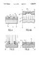
- FIGS. 1 to 4 and 1a to 4aillustrate a sequence of steps for selective metal deposition
- FIG. 5illustrates the process of the invention used for etching a substrate
- FIG. 6illustrates the process of the invention used for additive circuit formation.
- the process of the inventionis especially useful for the manufacture of electronic devices such as integrated circuits, multichip modules and printed circuit boards.
- the processis also useful for the fabrication of devices such as nameplates, relief plates, etc.
- electronic base materialmeans a substrate from which an electronic device is made such as a printed circuit board base material, a semiconductor, etc.
- the process of the inventionprovides a method for formation of metal deposits in a selective pattern over essentially any solid substrate.
- the processis especially useful for fabrication of high-density circuit boards with linewidths of 3 mils or less and integrated circuits with linewidths of 1 micron or less.
- a generalized processcould comprise the following steps:
- steps (b) and (c)may be reversed if provision is made to remove the ligating film from the surface of the photoresist prior to metallization using procedures to be discussed below.
- a photoresistcapable of providing high resolution images
- the exposure and formation of an image in the coatingprovides a relief image over the underlying substrate.
- the dimensions of the lines within the imageare limited only by the resolution capability of the photoresist. It is known in the art that photoresist may be processed to yield submicron images--i.e., images of 0.25 microns or less.
- a planarizing layeris coated over the substrate prior to application of the ligating film, especially for those applications where a step of etching the substrate is to be employed.
- the planarizing layerreduces surface reflection from the substrate that can interfere with image resolution and eliminates depth of focus limitations.
- the planarizing layermay be of a material capable of bonding with the ligating film more readily than the substrate material.
- the combination of the planarizing layer and the photoresist layeris preferred to a thick resist layer for enhanced image resolution.
- the step of contact of bared ligating groups with the electroless plating catalystresults in electroless plating catalyst bonding to the ligating groups exposed by development of the resist such as by coordination bonding.
- an electroless plating catalyst precursorin a selective pattern which may be metallized in said pattern and confined within the recesses of the photoresist image (Step (e)).
- the ligating layermay be provided over a substrate by any one of a variety of methods.
- Many substrate surfaces capable of being platedintrinsically contain chemical groups, or precursors of chemical groups, able to ligate with an electroless plating catalyst.
- Typical chemical groups capable of ligating with an electroless plating catalystcontain a donor atom selected from the group consisting of nitrogen, phosphorus, sulfur, oxygen and mixtures thereof.
- a polyvinylpyridine filmintrinsically contains such chemical groups with the pendant pyridine serving as the catalyst ligating group.
- the pyridyl grouphas been found to be a particularly preferred ligating group for a palladium catalyst.
- a substrate comprising aluminum oxidewill bind a palladium catalyst by the AlO and AlOH groups of the alumina.
- the ligating materialmay be physically blended as one component comprising the substrate if sufficient ligating moieties are accessible at the substrate surface to ligate with the catalyst.
- the surface of the substrateis modified to impart the necessary ligating groups to the surface.
- Substrate modification methodsinclude thermolysis, reaction of the surface with a chemical reagent, irradiation with photons or ions, vapor phase modification, graft polymerization, x-ray, nuclear radiation and by plasma oxidation or, more generally, any treatment that effects the desired conversion of the substrate.
- One potential modification sequenceprovides hydrolysis of a polyimide surface and reacting the hydrolyzed surface with a silane reagent possessing a suitable ligating group, such as ⁇ -trimethoxysilylethyl-2-pyridine.
- Another methodprovides chemically etching a polyethylene surface with a Cr 2 O 2- solution to provide hydroxyl groups on the substrate surface.
- the hydroxyl groupsshould then condense with a suitable compound containing a ligating group, for example nicotinoyl chloride with its pyridyl ligating group.
- the substrateis provided with ligating groups by coating with one or more film layers, each layer comprising one or more suitable ligating agents.
- the film layerpreferably adheres well to the substrate, for example by containing a functional group that will chemically and/or physically adhere to the substrate.
- the bonding and ligation functions of such ligating filmmay be performed by application of a single film or, alternatively, by application of multiple films with subsequent intermolecular linkage.
- ⁇ -trimethoxy-silylethyl-2-pyridineprovides both ligating and substrate-bonding functionalities.
- the alkoxysilane groupcan chemically bind the compound to a substrate.
- the trimethoxysilyl groupreacts with surface hydroxyl (silanol) functions of a quartz substrate, displacing methanol to directly bond to the substrate.
- the thus bound pyridyl moiety of the silylpyridyl moleculeserves as a ligand for chelating with the plating catalyst.
- the adhesive and ligating functionsmay be performed by multiple chemical groups with bond formation or other linkage between each of the groups.
- the linkage connecting the multiple functional groupsmay be of variable length and chemical composition. Examples include 3-(tri-methoxysilyl) propylamine and a quinoline-8-sulfonic acid chloride.
- the aminosilaneis applied as the substrate adsorbent.
- the coated surfaceis then reacted with a quinoline-8-sulfonic acid chloride, the SO 2 Cl group coupling to the amine group of the coated surface to form a sulfonamide linkage, and the quinolinic group serving as a catalyst ligation moiety.
- 3-(trimethoxysilyl) propylaminecan be applied to a substrate and then reacted with the acid chloride group of 4,4'-dicarbonyl chloride-2,2'-bipyridine to form an amide linkage.
- the pyridyl moieties of this complexserve as catalyst ligating groups.
- Other silyl aminescan be condensed in a similar manner, for example 3-(triethoxysilyl)propylamine.
- Another sequenceprovides condensing the hydroxyl groups of a chemically etched polyethylene substrate with a suitable ligating precursor, for example, 3-(trimethoxysilyl)propylamine, which after formation of the oxygen-silicon bond by methanol displacement, the amino group can condense with a suitable ligating compound such as nicotinoyl chloride.
- a suitable ligating precursorfor example, 3-(trimethoxysilyl)propylamine
- the ligating chemical group comprising a radiation sensitive chromophorecan provide selective photochemical patterning and metallization where selective photolysis or radiation ablation modifies the chemical groups on the substrate surface to substantially reduce or eliminate ligating ability in the selected film surface areas.
- a ligating filmcan be employed where selective photolysis transforms a non-ligating group within the film into a ligating group.
- the Photo-Fries reactionwhere a nitro aromatic compound rearranges to form a ligand is another potential means to provide suitable ligating groups. Though it is possible to utilize any of these reactions, they constitute a lesser preferred embodiment since photolysis of the ligating compound is unnecessary in accordance with the invention.
- the filmpreferably is an ultrathin self-assembled film, which is a film defined to mean a film having a thickness of between about ten molecular layers and a single molecular (monomolecular) layer.
- a filmcan be formed through dip coating, spin coating or vapor phase deposition procedures as are known in the art.
- the ligating filmprovides a substrate surface containing a chemical functional group capable of binding metallization catalysts from solution.
- a catalystto a surface is by a metal-ligand complexation, or ligation reaction.
- ligation reactionthe ability of a substrate ligand L to bind an electroless catalyst, for example a palladium (II) catalyst, should be readily determined by examining the formation equilibrium constant K f for the generalized complexation reaction (I):
- K fis equal to the ratio of concentration of products to reactants in reaction (I), i.e., ##EQU1##
- a chelate effecting a multidentate ligandprovides a greater K f than a corresponding monodentate group, where the term monodentate group refers to a chemical group that can provide only one ligand binding site, and the term multidentate group refers to chemical group or groups that can provide greater than one ligand binding site.
- monodentate grouprefers to a chemical group that can provide only one ligand binding site
- multidentate grouprefers to chemical group or groups that can provide greater than one ligand binding site.
- chelation of Ni(II) by 2,2'-bipyridineresults in a complex that is 10,000 times more stable than a pyridine complex, and 30 times more stable than a bis-pyridine complex.
- a higher K fprovides a metal deposit with relatively greater adhesion to a substrate upon subsequent metallization.
- a bipyridylis preferred over a monopyridyl for the relatively stronger bond the bipyridyl forms with an electroless metallization catalyst and the higher quality metal deposit thereby provided.
- Use of suitable multidentate ligating groupshas enabled deposition of thick adherent metal plates, including metal plates of thickness equal to and greater than about 2500 angstroms on smooth, unetched surfaces.
- numerous other multidentate groupsshould also serve as suitable ligating groups, for example, 2,2',6,2"-terpyridine, oxalate, ethylenediamine, 8-hydroxyquinoline and 1,10-phenanthroline.
- Organophosphines, nitriles, carboxylates and thiolsshould also ligate well, i.e., exhibit a significant K f , with a palladium electroless metallization catalyst.
- a palladium electroless metallization catalystfor example, 3-mercaptopropyltriethoxysilane, 2-(diphenylphosphino)-ethytriethoxysilane, and cyanomethylphenyltrimethoxysilane should serve as suitable catalyst ligating groups in accordance with the invention.
- ligating groups with antibonding (pi*) orbitals in the ligandfor example aromatic heterocycles such as pyridine and other nitrogen-containing aromatics.
- a variety of metal-containing compoundsmay be employed as the electroless catalyst precursor, such as palladium, platinum, rhodium, iridium, nickel, copper, silver and gold. Palladium or palladium-containing compounds are preferred. Particularly preferred palladium species include bis-(benzonitrile)palladium dichloride, palladium dichloride and Na 2 PdCl 4 .
- the electroless metallization catalystsare preferably applied to the substrate as an aqueous solution.
- Means for contacting a substrate with a catalyst solutionmay vary widely and include immersion of the substrate in a solution and spraying.
- the catalyst solution contact timecan vary with catalyst solution composition and age.
- the catalyst solutionmay comprise ancillary ligands, salts, buffers and other materials to enhance catalyst stability.
- Suitable agents for stabilizing a catalyst solutioncan vary with the particular catalyst employed.
- a metallization catalyst of PdCI 4 2-can be stabilized in aqueous solution by addition of excess chloride ion and decreasing pH to inhibit formation of oxo-bridged oligomers of the catalyst. Stabilization can be accomplished by adjustment of chloride ion concentration during preparation of the catalyst solution, or by adjustment of chloride ion concentration after the catalyst solution has attained full catalytic activity.
- other anions that prevent the formation of catalyst oligomersshould also be suitable agents for stabilizing a catalyst solution, for example, bromide and iodide ions.
- cation selectionmay be dictated by the specific metallization process. For example, for advanced microelectronic applications, use of sodium ions generally is avoided if possible and, therefore, use of tetraethylammonium chloride (TEACl) as a catalyst solution stabilizer may be preferred.
- TEACltetraethylammonium chloride
- catalyst solutions of higher (less acidic) pHe.g. pH of greater than 4
- a suitable buffer solutionPreferably, pH of a catalyst solution is controlled by a buffer component which does not appreciably coordinate with the metallization catalyst.
- catalyst solutionsmay be prepared using approximately equivalent initial quantities of acetate buffer, sodium chloride and Na 2 PdCl 4 .3H 2 O.
- An aqueous catalyst solutioncomprising NaCl and Na 2 PdCl 4 .3H 2 O reaches full activity as a metallization catalyst about 24 hours after preparation at room temperature.
- a catalyst solutioncan compete with the catalyst for binding with substrate ligating sites.
- the pK a values of the pyridyl groupsare about 4.44 and 2.6, for mono- and di-protonation respectively.
- HClmay protonate the pyridyl groups and effectively compete for these sites with the palladium catalyst.
- the substrate or electronic base material over which metal is to be depositedmay be permanent or temporary.
- a permanent substratemay comprise any of a known number of desired structures.
- the substratemay be a conventional printed circuit board, a molded circuit board, a hybrid circuit, a ceramic, a housing for an item of electronic equipment, a glass or quartz plate, etc.
- the substratemay be an existing circuit and the process of the invention may be used to form a multilayered circuit configuration.
- Another substratemay be an unclad plastic with multiple circuits built into a stack.
- the metal selectively depositedmay constitute circuit paths, metallized vias, etc. Other materials and configurations would be obvious to those skilled in the art.
- Suitable photoresists for these processesinclude those photoresists known to the art such as those described in numerous publications including DeForest, Photoresist Materials and Processes, McGraw-Hill Book Company, New York, Ch. 2, 1975 and Moreau, Semiconductor Lithography: Principles, Practices and Materials, Plenum Press, New York, Chs. 2 and 4, 1988, incorporated herein by reference.
- Positive working photoresiststypically are two-component systems comprising a radiation-sensitive compound in a film forming binder where the radiation-sensitive component undergoes photochemical alteration upon exposure.
- the two-component systemmay be dissolved in a suitable solvent to make a coating composition.
- the light-sensitive compounds most frequently used in two-component resist systemsare esters and amides formed from o-quinone diazide sulfonic and carboxylic acids, especially from sulfonic acid esters of naphthoquinone diazides. These esters and amides are well known and described by DeForest, supra, pages 47-55 and by Moreau, supra, pages 34-52.
- the light-sensitive compounds and the methods used to make the sameare all documented in prior patents including U.S. Pat. Nos. 3,046,110; 4,596,763; and 4,588,677, all incorporated herein by reference.
- the polymer binders most frequently used for positive working photoresists using o-quinone diazide sensitizersare the alkali soluble phenol formaldehyde resins known as the novolak resins. Photoresists using such polymers are illustrated in U.S. Pat. Nos. 4,377,631 and 4,404,272.
- Another class of binders used with o-quinone diazidesare homopolymers and copolymers of vinyl phenol. Photoresists of this nature are disclosed in U.S. Pat. No. 3,869,292.
- Single-component photoresistscomprise a polymer that undergoes chain scission.
- a photoresist using a polyglutarimide polymer as a binder alone or in combination with a photoactive componentis disclosed in U.S. Pat. No. 4,246,374 and further in U.S. Pat. No. 4,636,532.
- a photoresist using polymethylmethacrylate as a single component systemis disclosed in U.S. Pat. No. 4,584,309. Polyester and polyketone resists that are single-component positive resists are disclosed in U.S. Pat. No. 4,584,309.
- Negative-acting photoresistsare also suitable.
- a preferred class of such photoresistsare the acid hardening resists disclosed in EPO Application No. 0,232,972 which comprise an acid hardening resin, an aminoplast or phenoplast and a halogenated, organic, photoacid generating compound.
- Another preferred class of photoresistsare those disclosed and claimed in U.S. Pat. No. 4,877,818, incorporated herein by reference. These resists comprise at least one polymer having charged carrier groups, a photoinitiator and a source of unsaturation for crosslinking a film upon exposure to activating radiation.
- the photoresist coatingis desirably thin.
- the photoresist layerhas a dry coating thickness of between 50 and 500 nm and more preferably, between 75 and 250 nm.
- a planarizing layeris used to prevent reflection from the substrate. Suitable planarizing layers are disclosed in the examples that follow. Often, the planarizing layer contains a dye to absorb reflected light. The thickness of the planarizing layer is not critical but preferably varies between about 100 and 2,500 nm and more preferably, between 200 and 2,000 nm.
- Electroless metal deposition solutionsare those that deposit metal over a catalytically active surface by chemical reduction in the absence of an external electric current. Processes and compositions for electroless metal deposition are known in the art and are in substantial commercial use. They are disclosed in a number of prior art patents, for example, copper plating solutions are disclosed in U.S. Pat. Nos. 3,615,732; 3,615,733; 3,728,137; 3,846,138; 4,229,218; and 4,453,904, all incorporated herein by reference. Electroless nickel plating solutions are described in U.S. Pat. Nos.
- FIGS. 1 through 4depict process steps suitable for fabrication of a printed circuit board using the process of the invention with a positive acting photoresist.
- FIG. 1there is shown a substrate 10 coated with a ligand layer (in exaggerated proportion) 11.
- a substrate 10 coated with a ligand layerin exaggerated proportion
- the interface of the substrate 10 with ligand layer 11 lying between section lines A--A and B--Bis illustrated in FIG. 1A.
- the substrateis coated with a ligand layer having a terminus group bonded to the substrate, a second terminus group (L) capable of complexing with a catalytic metal ion open to the environment and the two terminus groups separated from each other by an inert spacer group such as a hydrocarbon chain.
- Lsecond terminus group
- FIG. 2illustrates a substrate 10 after it has been coated with a photoresist coating 12.
- the photoresisthas been applied, dried, imaged by exposure to activating radiation and developed to form a patterned resist coating over substrate 10.
- the imagemay be in the form of circuit paths or any other desired pattern.
- Developmenthas resulted in the formation of recesses within the photoresist coating baring ligand coating 11 where photoresist has been removed by development. This is shown in greater detail in FIG. 2A which represents both the interface of the ligand coating with substrate 10 and photoresist layer 12 in an imaged pattern.
- the next step in the process sequenceis illustrated in FIG. 3.
- the entire articlehas been contacted with a solution of plating catalyst to form catalytic layer 13.
- the plating catalystcombines with the ligand layer primarily where the catalytic solution is in contact with the ligand layer in areas by baring of the same through removal of resist depending upon the selectivity of the catalyst used. In this way, plating is restricted solely to those areas where plating metal is desired avoiding extraneous plating in undesired areas. For catalysts which are lesser selective in their ability to coordinate with the ligating material, an additional step of removal of undesired catalyst should be employed.
- the catalystcan be readily removed from an organic layer by contact of the layer with a solvent (a developer in the case of a photoresist) to remove the top surface of the layer together with extraneous catalyst. Moreover, there is no catalytic material in the interface between layers 10 and 12. If the article to be fabricated is a high density circuit board, the presence of catalytic material could result in unwanted conductive pathways between circuit lines. The combination of the catalytic material with the ligand layer is better illustrated in FIG. 3A.
- the substratemay be plated by contact with an electroless plating solution to form a metal deposit 14 within the recesses formed by the photoresist 12 as illustrated in FIGS. 4 and 4A.
- the metal deposit formedmay range in thickness from about 100 angstroms to several mils dependent upon the final use of the article.
- the thinner depositis suitable when the deposit is used as a plasma etch barrier and the thicker deposit is suitable for use of deposit as a circuit path in a fully additive procedure for circuit board fabrication.
- the thickness of the depositis dependent upon the immersion time in the plating solution, its temperature and the concentration of components within the solution.
- the photoresistmay be applied to the substrate prior to applying the ligand layer to the substrate.
- the substrate having the imaged photoresist coatingwould be contacted with the ligand solution to form a ligand layer over bared substrate surfaces, the sidewalls of the photoresist coating and its top surface.
- Metalcould then be selectively deposited by several alternative processes.
- the photoresistmay be stripped from the surface whereby the ligand will be removed with the photoresist leaving the ligand layer in a desired pattern on the substrate.
- the patterned ligand layermay then be metallized.
- the photoresist layer and bared substrate coated with the ligandmay be metallized with a thin layer of metal followed by stripping of the photoresist to remove the metal coating overlying the photoresist, but not the substrate.
- a disadvantage of this approachis a ragged edge on the remaining metal deposit.
- the remaining photoresist coatingmay be surface imaged and developed to remove the top surface of the photoresist coating and the ligand layer thereover. Thereafter, ligand bonded to the photoresist surface within the recesses of the coating and the bared substrate surface may be metallized. Finally, by proper selection of the ligand and appropriate conditioning of the substrate, the ligand could bond to the substrate without bonding to the photoresist. Thereafter, the ligand layer may be metallized in accordance with the procedures of the invention.
- the process of the inventionis well suited for plasma etching of substrates. This use is illustrated in FIG. 5 of the drawings where the article of FIG. 4 (having a thin deposit of plated metal) has been subjected to plasma etching whereby those areas of substrate 10 not protected by metal layer 14, have been etched. During etching, first the resist, then the ligand layer and finally substrate 10 is removed to depth D. The metal layer 13 protects the substrate from the plasma. Following plasma etching, the metal layer and ligand layer may be removed such as by contact with an acid or lifted off with a stripper if desired.
- the process of the inventionis also well suited for the formation of additive circuit boards. This use is illustrated in FIG. 6 of the drawings where in this instance, metal deposit 14 has been plated to full thickness of the recess.
- metal deposit 14has been plated to full thickness of the recess.
- the resist layer 12possesses suitable dielectric and thermal properties, it could remain as a permanent dielectric layer. Alternatively, it could be stripped from the substrate and replaced with a permanent dielectric material as would be understood by those skilled in the art.
- inorganic substratessilicon, silica, or quartz
- the substrateswere cleaned by immersion in a solution of 1:1 (v/v) concentrated hydrochloric acid: methanol for 30 minutes.
- the substrateswere then rinsed with deionized water and immersed in concentrated sulfuric acid for an additional 30 minutes, and then rinsed again with deionized water.
- the cleaned substrateswere then transferred to a container of gently boiling water where they were stored until needed.
- the cleaned substrateswere used directly from the water rinse.
- substrateswere dried under a stream of nitrogen gas passed through a 0.22 micron filter.
- the silica substrates usedwere fused silica slides 1 inch square obtained from Esco Products or Dell Optics. Silicon wafers were obtained from International Wafer Service.
- the catalyst solution used in the examples belowis prepared by dissolving 11.3 mg of sodium palladous chloride trihydrate and 1 ml of 1 molar aqueous sodium chloride solution. After the solids are dissolved, a 10 ml aliquot of pH 5 buffer solution (as prepared below) is added to the palladium solution and the contents are diluted to 100 ml with deionized water. After allowing the palladium solution to stand for 24 hours, a 10 ml aliquot is removed and replaced with an equal volume of 1 molar sodium chloride aqueous solution. All catalyst solutions used in the examples were used within one week of preparation.
- the buffer solutionwas made from 2-(N-morpholino)ethanesulfonic acid by adding 2.13 g. of said material to 50 ml. of water with stirring until dissolved. The solution is adjusted to pH with a dilute sodium hydroxide solution. The solution is then diluted to 100 ml. to produce the final buffer.
- the working bathwas prepared by mixing 4 ml of solution A with 88.5 ml of deionized water. To this solution was added 5 ml of solution M and then 2.5 ml of solution B. The bath was adjusted to pH 7.0 by addition of 0.1 molar sulfuric acid.
- the 100% cobalt metallization bathwas prepared immediately prior to use by mixing 3 volumes of a standard cobalt solution with 1 volume of a standard reducing solution.
- the standard cobalt solutionis prepared by dissolving 6 g. of cobalt chloride hexhydrate, 10 g of ammonium chloride and 9.8 g of ethylenediamine tetraacetic acid, tetrasodium salt and 100 ml of deionized water and adjusting the pH to 8.2 with 2 molar sodium hydroxide aqueous solution.
- the standard reducing solutionconsists of 8 g of dimethylamine borane complex and 100 ml. of deionized water.
- N-(2-aminoethyl)-3-aminopropyltrimethoxysilane(of formula (CH 3 O) 3 SiCH 2 CH 2 CH 2 NHCH 2 CH 2 NH 2 -- hereafter designated as EDA) were formed on three inch diameter Si wafers having a native oxide surface as follows. Under an inert atmosphere (He-filled dry box), a 1% (v/v) solution of a silane was prepared by adding the neat silane to methanol that had previously been acidified with 1 ⁇ 10 -3 M acetic acid. The solution was removed from the dry box, and 5% (by volume) deionized water was added. The cleaned substrates were transferred directly into the film deposition solution. After a 15 to 20 minute immersion at room temperature, the substrates were removed and rinsed in anhydrous methanol, and then baked on a hot plate for 3 to 5 minutes at 120° C.
- EDAN-(2-aminoethyl)-3-aminopropyltrimethoxysilane
- a water contact angle measurement (using the sessile drop method) of the freshly prepared EDA-treated surfaceyields a value of 17° to 25° C.
- the contact anglesslowly increased with time and reached stable values of about 30° C. within 12 hours after sample preparation.
- a UV absorption spectrum of an EDA coated fused silica slidegave no measurable absorption above 200 nm.
- the EDA coated waferswere catalyzed by contacting the wafer with catalyst solution for about 30 minutes. After this time, the catalyst solution was removed, the wafer rinsed with deionized water and dried under nitrogen. The wafers were then coated with SNRTM248-1.0 photoresist from Shipley Company Inc.
- SNR248is a deep UV sensitive, high resolution, negative working, chemically amplified photoresist that uses a poly(4-vinylphenol) resin binder and an acid catalyzed cross linking material.
- the resistwas applied to the substrates by spincoating using a spin speed of 4,000 rpm for 30 seconds, producing about a 1 ⁇ m thick coating. The resist was then pre-exposure baked at 90° C.
- the photoresistwas then exposed using patterned radiation from a Cymer CX-1 laser operating at 248 nm using KrF.
- the center of the laser beamwas passed through a circular aperture and then spread out by a diverging fused silica lens.
- the diverging beamwas then collimated through a fused silica lens to create a homogeneous beam with an average energy density of 1 mJ/cm 2 per pulse.
- a chrome-on-fused silica optical mask with feature sizes to 10 ⁇ mwas placed in direct mechanical contact with the photoresist coated wafers.
- This exampleis similar to Example 1 except catalysis follows application and imaging of the photoresist layer.
- Example 2Four inch diameter p-type ⁇ 100> Si wafers having a native oxide surface were treated with the ligating film as described in Example 1.
- SNR248 photoresistwas spin coated onto the substrate using a spin speed of 4100 rpm for 30 seconds to form a coating 0.96 ⁇ m thick and pre-exposure baked as in Example 1.
- the resistwas then exposed using patterned radiation from a GCA XLS 200 Laserstep 5 ⁇ reduction projection stepper using a line-narrowed KrF laser at 248 nm. Exposure doses ranged from 14.5-23.6 mJ/cm 2 .
- the resistwas post-exposure baked at 130° C. for 1 minute.
- the resistwas developed for 75 seconds using 0.14M NaOH and then rinsed with deionized water.
- the waferswere then inspected under an optical reflection microscope and exhibited the expected features with linewidths to about 2.5 ⁇ m. Features smaller than this value exhibited wavy lines of variable width, presumably due to insufficient adhesion of the resist to the silanized surface.
- the photoresist coated surface of the waferswas treated with the plating catalyst for 30 minutes, rinsed, and then immersed in the 10% nickel metallization bath for 30 minutes. The photoresist was stripped from the wafer by immersion in acetone for 3 minutes. Inspection under an optical microscope showed that nickel deposition occurred selectively on all the wafers, and the metal structures replicated the patterns previously observed in the developed regions of the resist. However, the exposed (crosslinked) photoresist was not completely stripped from some areas of the wafer with the acetone strip, even after a second immersion in acetone with application of ultrasound for several minutes.
- This examplerepeats Example 2 using an alternative stripping solution.
- Waferswere treated with the EDA silane, SNR248 photoresist, exposed, developed, catalyzed and metallized as described in Example 2.
- the waferwas immersed in XP91-140 remover from Shipley Company Inc. for 1 minute at 25° C. to strip the crosslinked photoresist. Identical metal patterns to those described in Example 2 were obtained, and no residual photoresist was present on the water.
- Example 2The procedure of Example 2 was repeated with a metal ion-free developer.
- Waferswere treated with the EDA silane, SNR248 photoresist, exposed, and post-exposure baked as in Example 2. Wafers were then immersed in Shipley XP89-114 developer (containing tetramethylammonium hydroxide as the active ingredient) for 2 minutes. Inspection of the wafers under an optical microscope showed the expected features with linewidths to about 1 ⁇ m, although some features with linewidths to about 0.5 ⁇ m were obtained. However, the majority of features with linewidths below 1 ⁇ m exhibited similar characteristics to the higher resolution features described in Example 2, presumably also due to insufficient adhesion of the resist to the silanized surface.
- the photoresist coated surface of the waferswas treated with the catalyst solution, rinsed, and then immersed in the 10% nickel metallization bath for 40 minutes.
- the photoresistwas stripped from the wafer by immersion in XP91-140 Remover for 1 minute. Inspection under an optical microscope showed that nickel deposition occurred selectively on all the wafers, and the metal structures replicated the patterns previously observed in the developed regions of the resist.
- Example 2The procedure of Example 2 was repeated except that PEDA was used to form the ligating film.
- Films(aminoethylaminomethyl)phenethyltrimethoxysilane (of formula (CH 3 O) 3 SiCH 2 CH 2 C 6 H 5 CH 2 NHCH 2 CH 2 NH 2 -- hereafter designated as PEDA) were prepared as follows. Under an inert atmosphere (He-filled dry box), a 1% (v/v) solution of silane was prepared by adding the neat silane to methanol that had previously been acidified with 1 ⁇ 10 -3 M acetic acid. The solution was removed from the dry box and 5% (by volume) deionized water was added. The cleaned substrates were transferred directly into the film deposition solution. After a 15 to 20 minute immersion at room temperature, the substrates were removed and rinsed in anhydrous methanol, and then baked on a hot plate for 3-5 minutes at 120° C.
- PEDAaminoethylaminomethylphenethyltrimethoxysilane
- a water contact angle measurement of the freshly prepared PEDA-treated surfaceyields a value of 64°-68° .
- a UV absorption spectrum of a PEDA-coated fused silica slideshows a maximum at about 200 nm and a shoulder at 220 nm with ⁇ about 5.5 ⁇ 10 4 M -1 cm -1 and about 1.8 ⁇ 10 4 M -1 cm -1 , respectively. These values of ⁇ are calculated from measured absorbance values and are based on a surface concentration of 10M and a path length of 1 ⁇ 10 -7 cm. Correspondence between the observed spectrum of PEDA on the fused silica surface and the spectrum in acetonitrile solution confirms the binding of the film to the substrate.
- PEDA-treated waferswere then coated with 0.96 ⁇ m of SNR248 photoresist, pre-exposure baked at 100° C. for 1 minute, exposed to 9.8-23.3 mJ/cm 2 of 248 nm radiation using the GCA XLS200 stepper, and post-exposure baked at 130° C. for 1 minute. Wafers were then puddle developed using XP89-114 developer for 125 seconds. Inspection of the wafers under an optical microscope showed the expected features with linewidths to about 1 ⁇ m, although some features with linewidths to about 0.5 ⁇ m were obtained.
- the photoresist coated surface of the waferswere catalyzed with the catalyst solution, rinsed, and then immersed in the nickel metallization bath for 40 minutes. Inspection of the wafers under an optical microscope showed that nickel deposition occurred selectively on all the wafers.
- the photoresistwas stripped from the wafer by immersion in XP91-140 Remover for 1 minute, and the wafers were re-examined in a scanning electron microscope. Metal features to submicron dimensions were observed.
- This exampledemonstrates the use of the photoresist masking process with the PEDA ligating film and with SAL-601 photoresist.
- Waferswere treated with the PEDA silane as described in Example 5, coated with 0.52 ⁇ m of SAL-601 photoresist by spin coating at 5000 rpm for 38 seconds.
- SAL-601is a deep UV (and also electron beam and x-ray) sensitive, high resolution, chemically amplified photoresist that employs a novolak resin.
- SAL-601is supplied by Shipley Company Inc.
- the resist coated waferswere pre-exposure baked at 100° C. for 1 minute, exposed to 9-41 mJ/cm 2 of 248 nm radiation using the GCA XLS200 stepper, and post-exposure baked at 110° C. for 1 minute. Wafers were then developed using 0.23M MF-312 developer from Shipley Company for 270 seconds.
- This exampledemonstrates the use of the photoresist masking process with the EDA ligating film and with PMMA electron beam resist on fused silica.
- a three inch square fused silica plate(Hoya Electric) was treated with EDA silane as described in Example 1.
- the substratewas then spincoated with PMMA (950,000 molecular weight, 6% solution from KTI) at 5K rpm for 30 seconds to give a film thickness of about 0.5 ⁇ m.
- the PMMAwas baked at 120° C. for 30 minutes.
- a 300 ⁇ chrome overcoatwas evaporated onto the surface of the PMMA to reduce charging effects during electron beam exposure.
- the resistwas exposed using a Cambridge EBMF6.5 electron-beam writer at a dose of 90 ⁇ m/cm 2 for feature sizes ranging from 1-10 ⁇ m. After exposure, the chrome layer was removed using a CR-9 stripping solution (Cyantek).
- the exposed PMMAwas developed by immersion in methyl isobutyl ketone for 90 seconds at room temperature.
- the patterned substratewas catalyzed with the catalyst solution for 30 minutes and then immersed in the nickel metallization bath for 40 minutes.
- the resistwas stripped by immersion in acetone for 5 minutes. Selective metallization of the substrate was observed at feature sizes to about 2 ⁇ m. Some excess metallization occurred on the surface of the PMMA.
- a second stripping procedure in which the substrate was sonicated in acetone for 5 minutesresulted in removal of most of the excess metal and did not damage any of the selectively metallized areas of the substrate.
- This exampledemonstrates the use of the photoresist masking process with SNR248 photoresist where the EDA ligand, catalyst, and electroless metal are applied after the resist is developed. The unwanted metal is then lifted off by stripping the resist.
- a Si wafer having a clean native oxide surfacewas coated with SNR248, pre-exposure baked, exposed with 248 nm light, post-exposure baked, and developed as described in Example 1 to create patterns (topography) in the resist.
- the waferwas then treated with the methanolic EDA solution described in Example 1, catalyzed with the catalyst solution for 30 minutes, and plated with 25% cobalt bath for about 10 minutes.
- the homogeneously plated, patterned waferswere treated with acetone at room temperature to dissolve the crosslinked resist, causing the metal on the exposed region to lift off along with the photoresist.
- This exampledemonstrates the use of the photoresist masking process with SNR248 photoresist and the EDA ligating film, where the unexposed resist is stripped prior to metallization.
- Example 8To minimize the edge roughness observed in Example 8, a similar process was performed except the resist stripping step was after catalysis, but before metallization.
- a Si waferwas coated with SNR248, softbaked, exposed through a contact mask to 50 mJ/cm 2 from a KrF excimer laser, postbaked, then developed for 3 minutes with XP89-114 developer.
- the patterned waferwas treated with the dilute EDA solution and then catalyzed with the catalyst solution for 15 minutes.
- the crosslinked resist remainingwas stripped with acetone and then immersed into a 25% cobalt plating bath for 10 minutes.
- Example 8This resulted in adherent cobalt patterns directly on the wafer, many with submicron edge roughness and 10 ⁇ m features resolved, a considerable improvement over the results of Example 8. However, in some areas of the wafer, excess unmetallized resist material was present which could not be stripped by longer immersion times in acetone. Characterization of the cobalt plated surface using Auger electron spectroscopy shows no palladium or copper in the exposed regions under the resist.
- This exampledemonstrates the use of the photoresist masking process with SNR248 photoresist and the EDA ligating film, where the unexposed resist is stripped prior to metallization.
- a Si waferwas processed in a similar manner to Example 9, except the methanolic EDA solution was used as both the developer and surface modification step. The wafer was then catalyzed, stripped, and plated as described above. This process gave similar resolution, adhesion (passes Scotch tape test), and excess unmetallized resist characteristics to the approach described in Example 9.
- This exampledemonstrates the use of the photoresist masking process with the PEDA ligating film and with S1400 photoresist on silicon.
- a Si waferwas treated with PEDA silane as described in Example 1. (In the rinse step after film formation both a deionized rinse and a 0.1M HCl rinse gave comparable results, indicating a lack of sensitivity of this process to a protonated surface film.)
- the waferwas then coated with about 1.0 ⁇ m of Shipley S1400-27 photoresist by spin coating at 4000 rpm for 30 seconds.
- S1400-27is a UV sensitive, high resolution, diazonapthoquinone based photoresist that employs a novolak resin.
- the resist coated waferswere pre-exposure baked at 90° C.
- the mask employedwas a chrome-on-fused silica plate with serpentine and cross-bridge structures having linewidths to 10 ⁇ m. Wafers were then developed using 0.27M (1:1 dilution of concentrate) MF-312 developer from Shipley Company for 45 seconds. Inspection of the wafers under an optical microscope showed the expected features (no evidence of adhesion loss) with linewidths to 10 ⁇ m--the minimum feature size on the mask.
- the photoresist coated surfaces of the waferswere catalyzed with the catalyst solution, rinsed, and then immersed in the nickel metallization bath for 20 minutes.
- the photoresistwas stripped from the wafer by immersion in acetone for about 30 seconds, rinsed with deionized water, and the wafer was dried under N 2 . Inspection of the wafer under an optical microscope showed the serpentine and cross-bridge structures replicated in nickel metal with the same feature sizes as on the mask.
- This exampledemonstrates the use of the photoresist masking process with the PEDA ligating film and with S1400 photoresist to produce submicron features on silicon.
- a Si waferwas treated with the PEDA silane, coated with S1400-27 photoresist, exposed using a high resolution transistor test structure mask, developed (40 seconds in MF-312), metallized, and stripped as described in Example 11. Inspection of the wafers under an optical microscope showed metal features with linewidths to ⁇ 1 ⁇ m.
- This exampledemonstrates the use of the photoresist masking process with the PEDA ligating film and with S1400 photoresist on CVD diamond.
- the waferwas placed in a Branson plasma etcher for 2 minutes at 100 W RF power using 150 sccm O 2 .
- the hydrophilic surfacewas then treated with the PEDA silane as described above.
- S1400-27 photoresistwas coated onto the wafer, exposed (serpentine mask), developed, catalyzed, and plated with nickel (for 2 hours) as described in Example 11. After resist removal with acetone, the wafer was inspected by optical and electron microscopy. Selective metal deposition was observed with feature sizes to 10 ⁇ m, the minimum linewidth present on the mask employed.
- This exampledemonstrates the use of the photoresist masking process with the UTF-15 ligating film and with S1400 photoresist on Si.
- UTF-15Films of 2-(trimethoxysilyl)ethyl-2-pyridine (of formula (CH 3 O) 3 SiCH 2 CH 2 C 5 H 4 N, hereafter designated as UTF-15) were prepared as follows. Under an inert atmosphere (He-filled dry box), a 1% (v/v) solution of UTF-15 was prepared by adding the neat silane to toluene that had previously been acidified with 10 -3 M acetic acid. The solution was removed from the dry box and the cleaned, dry substrates were transferred into the film deposition solution at room temperature. The solution was warmed for 60 minutes on a hotplate until the temperature of the solution reached 65° C. The substrates were removed from the solution and rinsed twice in fresh toluene, then baked for 3 minutes at 120° C. on a hotplate.
- a contact angle measurement of the surface of the slideyields a value of 45° .
- the UTF-15 treated substratewas then coated with S1400-27 photoresist, exposed, developed, catalyzed, metallized, and stripped as described in Example 11. Inspection of the wafer under an optical microscope showed the serpentine and cross-bridge structures replicated in nickel metal with the same feature sizes as on the mask.
- This exampledemonstrates the use of the photoresist masking process with the UTF-60 ligating film and with S1400 photoresist on Si.
- the UTF-60 treated substratewas then coated with S1400-27 photoresist, exposed, developed, catalyzed, metallized, and stripped as described in Example 11. Inspection of the wafer under an optical microscope showed the serpentine and cross-bridge structures replicated in nickel metal with the same feature sizes as on the mask.
- This exampledemonstrates the use of the photoresist masking process with the aqueous EDA ligating film and with S1400 photoresist to produce submicron features on silicon.
- a Si waferwas treated with the EDA silane as described in Example 1, with the exception that the treatment solution was entirely aqueous (1% silane in water with 1 ⁇ 10 -3 M acetic acid).
- the EDA treated waferwas then coated with S1400-27 photoresist, exposed using a standard UV contact aligner and a high resolution transistor test structure mask.
- the waferwas developed, metallized, and stripped as described in Example 11. Inspection of the wafers under an optical microscope showed metal features with linewidths to ⁇ 1 ⁇ m.
- This exampledemonstrates the use of the photoresist masking process with the aqueous DETA ligating film and with S1400 photoresist to produce about 0.5 ⁇ m thick metal features on Si.
- a Si waferwas treated with the aqueous DETA silane and processed as described in Example 16 for EDA, with the exception that the immersion time in the electroless nickel bath was 3 hours at a temperature of about 40° C. Inspection of the wafers under an optical microscope showed metal features with linewidths to ⁇ 1 ⁇ m. Surface profilometry showed the thickness of the metal features to be 0.47 ⁇ m.
- This exampledemonstrates the use of the photoresist masking process with the aqueous DETA ligating film and with S1400 photoresist to produce metal features on a cross-linked SNR248 polymeric planarizer.
- HMDShexamethyldisilazane
- SNR248 films(about 1 ⁇ m thick) were applied to the primed wafers by spincoating at 4000 rpm for 30 seconds.
- the SNR248 photoresistwas softbaked at 90° C. for 30 minutes on a vacuum hotplate, then thermally crosslinked by heating to 180° C. for 4 minutes.
- the crosslinked SNR248 photoresistserves as the planarizing layer.
- the SNR248 planarizing layerwas surface oxidized as described in Example 13, by exposure to an RF oxygen plasma at 100 W for 2 minutes.
- Contact angle using a water dropshowed that the initially hydrophobic (contact angle about 60°-70° ) SNR248 film became hydrophilic (contact angle ⁇ 20°) after plasma oxidation.
- Interferometric measurementsshowed that the SNR248 film thickness was essentially unchanged (within several nm) after plasma oxidation. This indicates that the plasma affects the functional groups in only the outer few nm of the film.
- Both waferswere then treated with a 1% aqueous DETA silane solution as described in Example 17.
- the silanized waferswere coated with S1400-27 photoresist by spin coating at 4000 rpm for 30 seconds and then pre-exposure baked at 90° C. for 30 minutes.
- the resist-coated waferswere exposed on a standard UV contact aligner using the serpentine mask for 18 seconds at 5 mW/cm 2 .
- Waferswere developed using 0.27M MF-312 developer for 60 seconds, then catalyzed with the catalyzing solution for 30 minutes and plated with electroless nickel for 20 minutes.
- This exampledemonstrates the use of the photoresist masking process with the aqueous DETA ligating film and with S1400 photoresist to produce metal features on an epoxy dielectric material.
- Metal serpentine patternswere produced homogeneously across the wafer.
- This exampledemonstrates the use of the photoresist masking process on epoxy dielectric material with an aged silane film.
- a Si wafer coated with an epoxy-based interlayer dielectric coatingwas processed as described in Example 19, except that the DETA-coated epoxy film was allowed to stand in the clean room for three days prior to application of the photoresist. Results obtained were identical to those in Example 19.
- This exampledemonstrates the use of the photoresist masking process with the aqueous EDA ligating film and with S1400 photoresist to produce metal features on an epoxy dielectric material.
- Example 19An epoxy-coated Si wafer was processed as described in Example 19, except that an aqueous solution of EDA (see Example 16) was used as the silanizing agent. Results obtained were identical to those in Example 19.
- This exampledemonstrates the use of the photoresist masking process on an epoxy planarizing layer to build up thick metal films.
- An epoxy-coated Si waferwas processed as described in Example 19, except the immersion time in the electroless nickel bath was 22 hours. Similar results were obtained to those in Example 19, except the thickness of the metal coating was about 0.5-0.55 ⁇ m, as determined by surface profilometry.
- This exampledemonstrates the use of the photoresist masking process with the aqueous DETA ligating film and with S1400 photoresist to produce submicron features on silicon.
- a Si waferwas coated with DETA silane from aqueous solution as described in Example 17.
- S1400-17 photoresistwas prepared by diluting S1400-27 to 63% of its original concentration with Shipley Thinner Type A.
- the photoresistwas spincoated at 4000 rpm for 30 seconds to give a thickness of 0.7 ⁇ m, then softbaked at 90° C. for 30 minutes.
- the resistwas exposed using a deep UV contact aligner with a high resolution grating mask for 4-5 seconds at 4 mW/cm 2 .
- the resistwas developed for 60 seconds in MF-312 (0.27M), catalyzed for 30 minutes with the catalyzing solution, metallized with electroless nickel for 20 minutes and then stripped by immersion in acetone for about 30 seconds. Inspection of the wafer by scanning electron microscopy showed selective deposition of metal grating structures homogeneously across the water with a minimum feature size of about 0.45 ⁇ m, corresponding to the minimum feature size present on the mask.
- This exampledemonstrates the use of the photoresist masking process with the aqueous DETA ligating film and with S1400 photoresist to produce metal features on a photochemically crosslinked SNR248 planarizer.
- a four inch diameter Si waferwas processed in a similar manner to that described in Example 18, with the following exceptions: the SNR248 planarizing layer was crosslinked by flood exposure for 2 minutes using the deep UV contact aligner at 4 mW/cm 2 , the crosslinked SNR248 was plasma oxidized as described for one of the wafers in Example 18. Selective metallization to produce the expected serpentine patterns was observed on both wafers. It was observed that the photochemical crosslinking produced a smoother photoresist surface (fewer bubbles or pits) than the thermal crosslinking procedure.
- the waferwas again flood exposed for 1 minute using a standard UV contact aligner at 5 mW/cm 2 to convert the initially unexposed resist to the exposed (soluble) form.
- the remaining exposed photoresistwas then stripped by immersion for 60 seconds in the 0.27M MF-312 developer solution.
- the photochemical stripping stepprovides an alternative method to stripping with acetone for situations in which an aqueous based solution is preferred as a stripping reagent.
- This exampledemonstrates the use of the photoresist masking process with the aqueous DETA ligating film and with S1400 photoresist using deep UV exposure to produce submicron metal features on a photochemically cross-linked SNR248 planarizer.
- a four inch diameter Si waferwas processed in a similar manner to that described in Example 24, with the following exceptions: S1400-17 photoresist was employed (as described in Example 23), and the resist was exposed with a high resolution grating mask on a deep UV contact aligner for 6-8 seconds at 4 mW/cm 2 . Selective metallization to produce grating structures with feature sizes to 0.6 ⁇ m was observed on the wafer.
- This exampledemonstrates the use of the photoresist masking process with the DETA ligating film and with S1400 photoresist on CVD diamond.
- a three inch Si wafer with a coating of CVD diamondwas processed as described in Example 13 with the following exceptions: the silanization was performed with aqueous DETA (see Example 17), development time was 70 seconds, and nickel plating time was 8 hours. Upon inspection by optical microscopy the wafer exhibited homogeneous, selective metal deposition with the expected serpentine features to 10 ⁇ m linewidth.
- This exampledemonstrates the use of the photoresist masking process with the aqueous DETA ligating film and with S1400 photoresist using an i-line projection stepper to produce submicron features on silicon.
- a Si waferwas processed as described in Example 23 with the exception that the S1400-17 photoresist was exposed using a GCA 0.45 NA i-line (365 nm) projection stepper.
- An exposure arraywas performed using a high resolution reticle with doses ranging from about 29-209 mJ/cm 2 . Inspection of the wafer after metallization and stripping with acetone showed production of metal features uniformly across the wafer. The minimum resolvable features were equal line/space pairs having linewidths to 0.40 ⁇ m.
- This exampleillustrates nickel deposition within a photoresist image using an aqueous EDA ligating film on silica and a 193 nm contact printer.
- a silicon waferwas coated with the EDA silane from the same aqueous solution used in Example 16.
- the EDA modified waferwas then coated with S1400-7 photoresist (a novolak-diazo based photoresist available from Shipley Company Inc.) to provide an approximately 115 nm thick film.
- the photoresistwas exposed to 20 mJ/cm 2 at 193 nm radiation using an ArF laser and a serpentine mask held in hard contact with the wafer.
- the exposed photoresist layerwas developed by immersion in MF 312 developer (aqueous alkaline solution) for 55 seconds and rinsed with deionized water.
- the waferwas catalyzed with Ac3 catalyst for thirty minutes and electrolessly plated with a 10% solution of NI 468 nickel plating solution at 22° C. for 20 minutes.
- the unexposed resistwas then stripped by spraying with acetone for 10 seconds. Inspection of the wafer showed metal features having line widths to 10 microns.
- Example 28This example is similar to Example 28 but utilizes a planarizing layer.
- a silicon waferwas coated with a novolak base planarizing film by spin coating at 3,000 rpm for 30 seconds.
- the planarizer filmwas soft baked at 100° C. for 1 minute on a vacuum hot plate and then hard baked at 140° C. for 1 minute.
- the planarizing filmwas then coated with EDA silane from aqueous solution as described in Example 16, rinsed with deionized water and baked at 120° C. for 5 minutes.
- the EDA modified planarizerwas coated with the photoresist of Example 28, exposed to 193 nm radiation, developed and then metallized using the procedure set forth in Example 28.
- the wafershowed metal features with serpentine features having line widths to 10 microns. Repeat of the process with exposure ranging between 15 and 20 mJ/cm 2 at 193 nm radiation through a high resolution mass grading yielded features with line widths to 1 micron.
- This exampleis similar to Example 28 but uses a standard UV exposure.
- a silicon waferwas coated with a novolak resin planarizing layer and silanized with EDA using the procedures of Example 29.
- the S1400-27 photoresistwas spin coated onto the planarizing layer to a thickness of 1 micron and exposed with a standard UV contact aligner for 22 seconds at 5 mW/cm 2 as described in Example 11.
- the resistwas developed and metallized with electroless nickel following procedures of Example 28.
- the wafershowed metal features having a serpentine configuration and line widths to 10 microns.
- This exampleis similar to Example 28 but uses deep UV exposure.
- a silicon waferwas coated with the novolak planarizing layer and silanized with EDA as described in Example 29.
- the S1400-17 photoresistwas coated onto the planarizing layer to a thickness of 0.5 microns, exposed with a deep UV (254 nm) contact aligner for 4 seconds at 4 mW/cm 2 using a high resolution mask.
- the resistwas developed for 45 seconds and metallized with electroless nickel using the procedures of Example 28.
- the remaining photoresistwas stripped. In one procedure, stripping was with an acetone spray. In another procedure, stripping was through the use of an RF oxygen plasma.
- the wafershowed metal features having line space features with line and space widths to 1 micron.
- This examplerepeats the process of Example 28 using i-line exposure.
- a silicon waferwas coated with a novolak planarizing layer and silanized with EDA following the procedures of Example 29.
- a layer of S1400-17 photoresistwas spin coated onto the planarizing layer to a thickness of 0.5 microns and exposed with an i-line (365 nm) projection exposure tool for doses ranging from 10-160 mJ/cm 2 .
- the resistwas developed for 75 seconds, and metallized with an electroless nickel coating as described in Example 28.
- the wafershowed metal features of various test patterns with linewidths to 0.6 microns.
Landscapes
- Chemical & Material Sciences (AREA)
- General Chemical & Material Sciences (AREA)
- Chemical Kinetics & Catalysis (AREA)
- Engineering & Computer Science (AREA)
- Materials Engineering (AREA)
- Mechanical Engineering (AREA)
- Metallurgy (AREA)
- Organic Chemistry (AREA)
- Inorganic Chemistry (AREA)
- Physics & Mathematics (AREA)
- General Physics & Mathematics (AREA)
- Chemically Coating (AREA)
- ing And Chemical Polishing (AREA)
- Electrodes Of Semiconductors (AREA)
- Manufacturing Of Printed Circuit Boards (AREA)
- Manufacturing Of Printed Wiring (AREA)
Abstract
Description
Pd.sup.2+ +L⃡PdL.sup.2+ (I)
Claims (18)
Priority Applications (3)
| Application Number | Priority Date | Filing Date | Title |
|---|---|---|---|
| US08/111,640US5468597A (en) | 1993-08-25 | 1993-08-25 | Selective metallization process |
| JP6224208AJPH07166372A (en) | 1993-08-25 | 1994-08-25 | Method for selective metallization |
| US08/520,554US5510216A (en) | 1993-08-25 | 1995-08-29 | Selective metallization process |
Applications Claiming Priority (1)
| Application Number | Priority Date | Filing Date | Title |
|---|---|---|---|
| US08/111,640US5468597A (en) | 1993-08-25 | 1993-08-25 | Selective metallization process |
Related Child Applications (1)
| Application Number | Title | Priority Date | Filing Date |
|---|---|---|---|
| US22635294ADivision | 1993-08-25 | 1994-04-12 |
Publications (1)
| Publication Number | Publication Date |
|---|---|
| US5468597Atrue US5468597A (en) | 1995-11-21 |
Family
ID=22339624
Family Applications (2)
| Application Number | Title | Priority Date | Filing Date |
|---|---|---|---|
| US08/111,640Expired - LifetimeUS5468597A (en) | 1993-08-25 | 1993-08-25 | Selective metallization process |
| US08/520,554Expired - Fee RelatedUS5510216A (en) | 1993-08-25 | 1995-08-29 | Selective metallization process |
Family Applications After (1)
| Application Number | Title | Priority Date | Filing Date |
|---|---|---|---|
| US08/520,554Expired - Fee RelatedUS5510216A (en) | 1993-08-25 | 1995-08-29 | Selective metallization process |
Country Status (2)
| Country | Link |
|---|---|
| US (2) | US5468597A (en) |
| JP (1) | JPH07166372A (en) |
Cited By (39)
| Publication number | Priority date | Publication date | Assignee | Title |
|---|---|---|---|---|
| US5667922A (en)* | 1996-04-26 | 1997-09-16 | Allegro Microsystems, Inc. | Method of semiconductor fabrication utilizing rinse of polyimide film |
| US5725807A (en) | 1993-05-17 | 1998-03-10 | Electrochemicals Inc. | Carbon containing composition for electroplating |
| WO1999013994A1 (en)* | 1997-09-16 | 1999-03-25 | Sri International | Deposition of substances on a surface |
| US6114099A (en)* | 1996-11-21 | 2000-09-05 | Virginia Tech Intellectual Properties, Inc. | Patterned molecular self-assembly |
| US6146716A (en)* | 1998-06-26 | 2000-11-14 | Sri International | Conservatively printed displays and methods relating to same |
| US6171468B1 (en) | 1993-05-17 | 2001-01-09 | Electrochemicals Inc. | Direct metallization process |
| US6174650B1 (en)* | 1997-01-23 | 2001-01-16 | Matsushita Electric Industrial Co., Ltd. | Manufacturing method and apparatus for semiconductor device |
| US6174647B1 (en)* | 1998-01-26 | 2001-01-16 | Shipley Company, L.L.C. | Metallization process and component |
| US6194127B1 (en) | 1998-05-27 | 2001-02-27 | Mcdonnell Douglas Corporation | Resistive sheet patterning process and product thereof |
| US6265075B1 (en) | 1999-07-20 | 2001-07-24 | International Business Machines Corporation | Circuitized semiconductor structure and method for producing such |
| US6303181B1 (en) | 1993-05-17 | 2001-10-16 | Electrochemicals Inc. | Direct metallization process employing a cationic conditioner and a binder |
| US6436615B1 (en)* | 1999-06-25 | 2002-08-20 | The United States Of America As Represented By The Secretary Of The Navy | Methods and materials for selective modification of photopatterned polymer films |
| US20020142092A1 (en)* | 2000-03-27 | 2002-10-03 | Klaus Lowack | Method for the metalization of an insulator and/or a dielectric |
| WO2003024174A1 (en)* | 2001-09-05 | 2003-03-20 | Zeon Corporation | Mulitilayer circuit board, resin base material, and its production method |
| WO2002078102A3 (en)* | 2001-03-21 | 2003-10-16 | Hewlett Packard Co | Fabricating a molecular electronic device having a protective barrier layer |
| US6710259B2 (en) | 1993-05-17 | 2004-03-23 | Electrochemicals, Inc. | Printed wiring boards and methods for making them |
| US6733868B1 (en) | 1998-05-14 | 2004-05-11 | Seiko Epson Corporation | Substrate for forming specific pattern, and method for manufacturing same |
| US20040159633A1 (en)* | 1993-10-04 | 2004-08-19 | President & Fellows Of Harvard University | Methods of etching articles via micro contact printing |
| US20040180506A1 (en)* | 2000-10-12 | 2004-09-16 | G. Ramanath | Diffusion barriers comprising a self-assembled monolayer |
| US20040247797A1 (en)* | 2003-03-26 | 2004-12-09 | Toshimitsu Hirai | Device, method of manufacturing the same, electro-optic device, and electronic equipment |
| US20040245518A1 (en)* | 2003-06-06 | 2004-12-09 | Rensselaer Polytechnic Institute | Self-assembled sub-nanolayers as interfacial adhesion enhancers and diffusion barriers |
| US20050031788A1 (en)* | 2003-07-02 | 2005-02-10 | Rohm And Haas Electronic Materials, L.L.C. | Metallization of ceramics |
| US20050092761A1 (en)* | 2003-11-03 | 2005-05-05 | Marganski Paul J. | Fluid storage and dispensing vessels having colorimetrically veriflable leak-tightness, and method of making same |
| US6916741B2 (en)* | 2000-05-08 | 2005-07-12 | Shipley Company, L.L.C. | Capture compounds for electronic plating compositions and electronic packaging device manufacture |
| US20050238968A1 (en)* | 2002-05-17 | 2005-10-27 | Caspar Jonathan V | Planarizing element for thermal printing of color filter |
| US20070264833A1 (en)* | 2006-05-11 | 2007-11-15 | Hitachi Global Storage Technologies | High resolution patterning of surface energy utilizing high resolution monomolecular resist for fabrication of patterned media masters |
| CN102752962A (en)* | 2011-04-21 | 2012-10-24 | 明阅科技有限公司 | Substrate with metal layer and manufacturing method thereof |
| TWI405869B (en)* | 2009-12-17 | 2013-08-21 | Perusetech Company | Substrate with metal layer and method for manufacturing the same |
| US20130260058A1 (en)* | 2002-12-14 | 2013-10-03 | Plastic Logic Limited | Electronic devices |
| US20140178571A1 (en)* | 2011-05-30 | 2014-06-26 | Akimitsu Bamba | Resin substrate having metal film pattern formed thereon |
| US20140287563A1 (en)* | 2013-03-22 | 2014-09-25 | Kabushiki Kaisha Toshiba | Method of manufacturing semiconductor device |
| JP2015089951A (en)* | 2013-11-05 | 2015-05-11 | キヤノン・コンポーネンツ株式会社 | Article with metallic film and production method thereof, and wiring board |
| US9088074B2 (en) | 2011-07-14 | 2015-07-21 | Nuvotronics, Llc | Hollow core coaxial cables and methods of making the same |
| US9305807B2 (en)* | 2014-02-27 | 2016-04-05 | Palo Alto Research Center Incorporated | Fabrication method for microelectronic components and microchip inks used in electrostatic assembly |
| US20190010608A1 (en)* | 2016-03-31 | 2019-01-10 | Fujifilm Corporation | Method for producing electroconductive laminate, laminate, and electroconductive laminate |
| US20200232098A1 (en)* | 2019-01-22 | 2020-07-23 | Averatek Corporation | Pattern formation using catalyst blocker |
| US20200251332A1 (en)* | 2019-02-06 | 2020-08-06 | Intel Corporation | Selective metal deposition by patterning direct electroless metal plating |
| TWI737835B (en)* | 2016-10-27 | 2021-09-01 | 日商東京威力科創股份有限公司 | Plating treatment method, plating treatment device and storage medium |
| WO2023113866A1 (en)* | 2021-12-17 | 2023-06-22 | Applied Materials, Inc. | Self-assembled monolayer for selective deposition |
Families Citing this family (213)
| Publication number | Priority date | Publication date | Assignee | Title |
|---|---|---|---|---|
| JP3961092B2 (en)* | 1997-06-03 | 2007-08-15 | 株式会社東芝 | Composite wiring board, flexible substrate, semiconductor device, and method of manufacturing composite wiring board |
| US6276072B1 (en)* | 1997-07-10 | 2001-08-21 | Applied Materials, Inc. | Method and apparatus for heating and cooling substrates |
| JP3598317B2 (en)* | 1999-01-20 | 2004-12-08 | 独立行政法人産業技術総合研究所 | Pretreatment method for electroless plating |
| US7192494B2 (en) | 1999-03-05 | 2007-03-20 | Applied Materials, Inc. | Method and apparatus for annealing copper films |
| US6277544B1 (en)* | 1999-06-09 | 2001-08-21 | Advanced Micro Devices, Inc. | Reverse lithographic process for semiconductor spaces |
| US6221777B1 (en) | 1999-06-09 | 2001-04-24 | Advanced Micro Devices, Inc. | Reverse lithographic process for semiconductor vias |
| US6258223B1 (en) | 1999-07-09 | 2001-07-10 | Applied Materials, Inc. | In-situ electroless copper seed layer enhancement in an electroplating system |
| US7059948B2 (en)* | 2000-12-22 | 2006-06-13 | Applied Materials | Articles for polishing semiconductor substrates |
| JP4581182B2 (en)* | 2000-05-26 | 2010-11-17 | 株式会社村田製作所 | Conductor forming method and electronic component |
| US20040079633A1 (en)* | 2000-07-05 | 2004-04-29 | Applied Materials, Inc. | Apparatus for electro chemical deposition of copper metallization with the capability of in-situ thermal annealing |
| US6835534B2 (en)* | 2000-10-27 | 2004-12-28 | The Penn State Research Foundation | Chemical functionalization nanolithography |
| US6815359B2 (en)* | 2001-03-28 | 2004-11-09 | Advanced Micro Devices, Inc. | Process for improving the etch stability of ultra-thin photoresist |
| US6716571B2 (en)* | 2001-03-28 | 2004-04-06 | Advanced Micro Devices, Inc. | Selective photoresist hardening to facilitate lateral trimming |
| US6774365B2 (en)* | 2001-03-28 | 2004-08-10 | Advanced Micro Devices, Inc. | SEM inspection and analysis of patterned photoresist features |
| US6586158B2 (en)* | 2001-05-25 | 2003-07-01 | The United States Of America As Represented By The Secretary Of The Navy | Anti-charging layer for beam lithography and mask fabrication |
| EP1432857A1 (en)* | 2001-09-07 | 2004-06-30 | Borden Chemical, Inc. | Coated optical fibers using adhesion promoters, and methods for making and using same |
| US7862860B2 (en)* | 2001-11-29 | 2011-01-04 | International Business Machines Corporation | Materials and methods for immobilization of catalysts on surfaces and for selective electroless metallization |
| US7087267B2 (en)* | 2001-11-29 | 2006-08-08 | International Business Machines Corporation | Materials and methods for immobilization of catalysts on surfaces and for selective electroless metallization |
| US6824666B2 (en)* | 2002-01-28 | 2004-11-30 | Applied Materials, Inc. | Electroless deposition method over sub-micron apertures |
| US7138014B2 (en)* | 2002-01-28 | 2006-11-21 | Applied Materials, Inc. | Electroless deposition apparatus |
| US6905622B2 (en)* | 2002-04-03 | 2005-06-14 | Applied Materials, Inc. | Electroless deposition method |
| US6899816B2 (en)* | 2002-04-03 | 2005-05-31 | Applied Materials, Inc. | Electroless deposition method |
| US20030207206A1 (en)* | 2002-04-22 | 2003-11-06 | General Electric Company | Limited play data storage media and method for limiting access to data thereon |
| US6875691B2 (en)* | 2002-06-21 | 2005-04-05 | Mattson Technology, Inc. | Temperature control sequence of electroless plating baths |
| US6821909B2 (en)* | 2002-10-30 | 2004-11-23 | Applied Materials, Inc. | Post rinse to improve selective deposition of electroless cobalt on copper for ULSI application |
| US6797312B2 (en)* | 2003-01-21 | 2004-09-28 | Mattson Technology, Inc. | Electroless plating solution and process |
| US6887776B2 (en)* | 2003-04-11 | 2005-05-03 | Applied Materials, Inc. | Methods to form metal lines using selective electrochemical deposition |
| US7654221B2 (en)* | 2003-10-06 | 2010-02-02 | Applied Materials, Inc. | Apparatus for electroless deposition of metals onto semiconductor substrates |
| US7827930B2 (en)* | 2004-01-26 | 2010-11-09 | Applied Materials, Inc. | Apparatus for electroless deposition of metals onto semiconductor substrates |
| US20070111519A1 (en)* | 2003-10-15 | 2007-05-17 | Applied Materials, Inc. | Integrated electroless deposition system |
| US7064065B2 (en)* | 2003-10-15 | 2006-06-20 | Applied Materials, Inc. | Silver under-layers for electroless cobalt alloys |
| US7465358B2 (en)* | 2003-10-15 | 2008-12-16 | Applied Materials, Inc. | Measurement techniques for controlling aspects of a electroless deposition process |
| US20050095830A1 (en)* | 2003-10-17 | 2005-05-05 | Applied Materials, Inc. | Selective self-initiating electroless capping of copper with cobalt-containing alloys |
| WO2005038084A2 (en)* | 2003-10-17 | 2005-04-28 | Applied Materials, Inc. | Selective self-initiating electroless capping of copper with cobalt-containing alloys |
| US7205233B2 (en)* | 2003-11-07 | 2007-04-17 | Applied Materials, Inc. | Method for forming CoWRe alloys by electroless deposition |
| US20060003570A1 (en)* | 2003-12-02 | 2006-01-05 | Arulkumar Shanmugasundram | Method and apparatus for electroless capping with vapor drying |
| US20050178666A1 (en)* | 2004-01-13 | 2005-08-18 | Applied Materials, Inc. | Methods for fabrication of a polishing article |
| US20060033678A1 (en)* | 2004-01-26 | 2006-02-16 | Applied Materials, Inc. | Integrated electroless deposition system |
| US20050170650A1 (en)* | 2004-01-26 | 2005-08-04 | Hongbin Fang | Electroless palladium nitrate activation prior to cobalt-alloy deposition |
| US20050181226A1 (en)* | 2004-01-26 | 2005-08-18 | Applied Materials, Inc. | Method and apparatus for selectively changing thin film composition during electroless deposition in a single chamber |
| US20050161338A1 (en)* | 2004-01-26 | 2005-07-28 | Applied Materials, Inc. | Electroless cobalt alloy deposition process |
| US20050230350A1 (en)* | 2004-02-26 | 2005-10-20 | Applied Materials, Inc. | In-situ dry clean chamber for front end of line fabrication |
| JP3879856B2 (en)* | 2004-03-30 | 2007-02-14 | セイコーエプソン株式会社 | Wiring board manufacturing method and electronic device manufacturing method |
| US20050253268A1 (en)* | 2004-04-22 | 2005-11-17 | Shao-Ta Hsu | Method and structure for improving adhesion between intermetal dielectric layer and cap layer |
| US20060240187A1 (en)* | 2005-01-27 | 2006-10-26 | Applied Materials, Inc. | Deposition of an intermediate catalytic layer on a barrier layer for copper metallization |
| US20060246217A1 (en)* | 2005-03-18 | 2006-11-02 | Weidman Timothy W | Electroless deposition process on a silicide contact |
| US7651934B2 (en) | 2005-03-18 | 2010-01-26 | Applied Materials, Inc. | Process for electroless copper deposition |
| US20060246699A1 (en)* | 2005-03-18 | 2006-11-02 | Weidman Timothy W | Process for electroless copper deposition on a ruthenium seed |
| US20060252252A1 (en)* | 2005-03-18 | 2006-11-09 | Zhize Zhu | Electroless deposition processes and compositions for forming interconnects |
| US20060257785A1 (en)* | 2005-05-13 | 2006-11-16 | Johnson Donald W | Method of forming a photoresist element |
| MY142216A (en)* | 2005-05-20 | 2010-11-15 | Fuji Photo Film Co Ltd | Graft pattern forming method and conductive pattern forming method |
| JP4628914B2 (en)* | 2005-09-20 | 2011-02-09 | 株式会社大和化成研究所 | Circuit pattern forming method |
| WO2007035880A2 (en)* | 2005-09-21 | 2007-03-29 | Applied Materials, Inc. | Method and apparatus for forming device features in an integrated electroless deposition system |
| US20070099422A1 (en)* | 2005-10-28 | 2007-05-03 | Kapila Wijekoon | Process for electroless copper deposition |
| US20070099806A1 (en)* | 2005-10-28 | 2007-05-03 | Stewart Michael P | Composition and method for selectively removing native oxide from silicon-containing surfaces |
| US7678704B2 (en)* | 2005-12-13 | 2010-03-16 | Infineon Technologies Ag | Method of making a contact in a semiconductor device |
| KR101551501B1 (en)* | 2007-03-10 | 2015-09-08 | 산미나 코포레이션 | embedded capacitive stack |
| US7867900B2 (en)* | 2007-09-28 | 2011-01-11 | Applied Materials, Inc. | Aluminum contact integration on cobalt silicide junction |
| JP5707709B2 (en)* | 2009-03-23 | 2015-04-30 | 富士電機株式会社 | Manufacturing method of semiconductor device |
| US8974860B2 (en)* | 2009-06-19 | 2015-03-10 | Robert Hamilton | Selective deposition of metal on plastic substrates |
| US9324576B2 (en) | 2010-05-27 | 2016-04-26 | Applied Materials, Inc. | Selective etch for silicon films |
| US10283321B2 (en) | 2011-01-18 | 2019-05-07 | Applied Materials, Inc. | Semiconductor processing system and methods using capacitively coupled plasma |
| US8771539B2 (en) | 2011-02-22 | 2014-07-08 | Applied Materials, Inc. | Remotely-excited fluorine and water vapor etch |
| US9064815B2 (en) | 2011-03-14 | 2015-06-23 | Applied Materials, Inc. | Methods for etch of metal and metal-oxide films |
| US8999856B2 (en) | 2011-03-14 | 2015-04-07 | Applied Materials, Inc. | Methods for etch of sin films |
| US8771536B2 (en) | 2011-08-01 | 2014-07-08 | Applied Materials, Inc. | Dry-etch for silicon-and-carbon-containing films |
| US8679982B2 (en) | 2011-08-26 | 2014-03-25 | Applied Materials, Inc. | Selective suppression of dry-etch rate of materials containing both silicon and oxygen |
| US8679983B2 (en) | 2011-09-01 | 2014-03-25 | Applied Materials, Inc. | Selective suppression of dry-etch rate of materials containing both silicon and nitrogen |
| US8927390B2 (en) | 2011-09-26 | 2015-01-06 | Applied Materials, Inc. | Intrench profile |
| US8808563B2 (en) | 2011-10-07 | 2014-08-19 | Applied Materials, Inc. | Selective etch of silicon by way of metastable hydrogen termination |
| WO2013070436A1 (en) | 2011-11-08 | 2013-05-16 | Applied Materials, Inc. | Methods of reducing substrate dislocation during gapfill processing |
| US9267739B2 (en) | 2012-07-18 | 2016-02-23 | Applied Materials, Inc. | Pedestal with multi-zone temperature control and multiple purge capabilities |
| US9373517B2 (en) | 2012-08-02 | 2016-06-21 | Applied Materials, Inc. | Semiconductor processing with DC assisted RF power for improved control |
| US9034770B2 (en) | 2012-09-17 | 2015-05-19 | Applied Materials, Inc. | Differential silicon oxide etch |
| US9023734B2 (en) | 2012-09-18 | 2015-05-05 | Applied Materials, Inc. | Radical-component oxide etch |
| US9390937B2 (en) | 2012-09-20 | 2016-07-12 | Applied Materials, Inc. | Silicon-carbon-nitride selective etch |
| US9132436B2 (en) | 2012-09-21 | 2015-09-15 | Applied Materials, Inc. | Chemical control features in wafer process equipment |
| US8765574B2 (en) | 2012-11-09 | 2014-07-01 | Applied Materials, Inc. | Dry etch process |
| US8969212B2 (en) | 2012-11-20 | 2015-03-03 | Applied Materials, Inc. | Dry-etch selectivity |
| US8980763B2 (en) | 2012-11-30 | 2015-03-17 | Applied Materials, Inc. | Dry-etch for selective tungsten removal |
| US9064816B2 (en) | 2012-11-30 | 2015-06-23 | Applied Materials, Inc. | Dry-etch for selective oxidation removal |
| US9111877B2 (en) | 2012-12-18 | 2015-08-18 | Applied Materials, Inc. | Non-local plasma oxide etch |
| US8921234B2 (en) | 2012-12-21 | 2014-12-30 | Applied Materials, Inc. | Selective titanium nitride etching |
| US10256079B2 (en) | 2013-02-08 | 2019-04-09 | Applied Materials, Inc. | Semiconductor processing systems having multiple plasma configurations |
| US9362130B2 (en) | 2013-03-01 | 2016-06-07 | Applied Materials, Inc. | Enhanced etching processes using remote plasma sources |
| US9040422B2 (en) | 2013-03-05 | 2015-05-26 | Applied Materials, Inc. | Selective titanium nitride removal |
| US8801952B1 (en) | 2013-03-07 | 2014-08-12 | Applied Materials, Inc. | Conformal oxide dry etch |
| US10170282B2 (en) | 2013-03-08 | 2019-01-01 | Applied Materials, Inc. | Insulated semiconductor faceplate designs |
| US20140271097A1 (en) | 2013-03-15 | 2014-09-18 | Applied Materials, Inc. | Processing systems and methods for halide scavenging |
| US8895449B1 (en) | 2013-05-16 | 2014-11-25 | Applied Materials, Inc. | Delicate dry clean |
| US9114438B2 (en) | 2013-05-21 | 2015-08-25 | Applied Materials, Inc. | Copper residue chamber clean |
| US9493879B2 (en) | 2013-07-12 | 2016-11-15 | Applied Materials, Inc. | Selective sputtering for pattern transfer |
| JP5643911B1 (en)* | 2013-08-09 | 2014-12-17 | キヤノン・コンポーネンツ株式会社 | Method for manufacturing substrate with metal film, substrate with metal film, and wiring board |
| US9773648B2 (en) | 2013-08-30 | 2017-09-26 | Applied Materials, Inc. | Dual discharge modes operation for remote plasma |
| US8956980B1 (en) | 2013-09-16 | 2015-02-17 | Applied Materials, Inc. | Selective etch of silicon nitride |
| US8951429B1 (en) | 2013-10-29 | 2015-02-10 | Applied Materials, Inc. | Tungsten oxide processing |
| US9236265B2 (en) | 2013-11-04 | 2016-01-12 | Applied Materials, Inc. | Silicon germanium processing |
| US9576809B2 (en) | 2013-11-04 | 2017-02-21 | Applied Materials, Inc. | Etch suppression with germanium |
| US9520303B2 (en) | 2013-11-12 | 2016-12-13 | Applied Materials, Inc. | Aluminum selective etch |
| TWI692546B (en)* | 2013-11-21 | 2020-05-01 | 日商尼康股份有限公司 | Wiring pattern manufacturing method and transistor manufacturing method |
| US9245762B2 (en) | 2013-12-02 | 2016-01-26 | Applied Materials, Inc. | Procedure for etch rate consistency |
| US9117855B2 (en) | 2013-12-04 | 2015-08-25 | Applied Materials, Inc. | Polarity control for remote plasma |
| US9287095B2 (en) | 2013-12-17 | 2016-03-15 | Applied Materials, Inc. | Semiconductor system assemblies and methods of operation |
| US9263278B2 (en) | 2013-12-17 | 2016-02-16 | Applied Materials, Inc. | Dopant etch selectivity control |
| US9190293B2 (en) | 2013-12-18 | 2015-11-17 | Applied Materials, Inc. | Even tungsten etch for high aspect ratio trenches |
| US9287134B2 (en) | 2014-01-17 | 2016-03-15 | Applied Materials, Inc. | Titanium oxide etch |
| US9293568B2 (en) | 2014-01-27 | 2016-03-22 | Applied Materials, Inc. | Method of fin patterning |
| US9396989B2 (en) | 2014-01-27 | 2016-07-19 | Applied Materials, Inc. | Air gaps between copper lines |
| US9385028B2 (en) | 2014-02-03 | 2016-07-05 | Applied Materials, Inc. | Air gap process |
| US9499898B2 (en) | 2014-03-03 | 2016-11-22 | Applied Materials, Inc. | Layered thin film heater and method of fabrication |
| US9299575B2 (en) | 2014-03-17 | 2016-03-29 | Applied Materials, Inc. | Gas-phase tungsten etch |
| US9299537B2 (en) | 2014-03-20 | 2016-03-29 | Applied Materials, Inc. | Radial waveguide systems and methods for post-match control of microwaves |
| US9299538B2 (en) | 2014-03-20 | 2016-03-29 | Applied Materials, Inc. | Radial waveguide systems and methods for post-match control of microwaves |
| US9136273B1 (en) | 2014-03-21 | 2015-09-15 | Applied Materials, Inc. | Flash gate air gap |
| US9903020B2 (en) | 2014-03-31 | 2018-02-27 | Applied Materials, Inc. | Generation of compact alumina passivation layers on aluminum plasma equipment components |
| US9269590B2 (en) | 2014-04-07 | 2016-02-23 | Applied Materials, Inc. | Spacer formation |
| US9309598B2 (en) | 2014-05-28 | 2016-04-12 | Applied Materials, Inc. | Oxide and metal removal |
| US9847289B2 (en) | 2014-05-30 | 2017-12-19 | Applied Materials, Inc. | Protective via cap for improved interconnect performance |
| US9378969B2 (en) | 2014-06-19 | 2016-06-28 | Applied Materials, Inc. | Low temperature gas-phase carbon removal |
| US9406523B2 (en) | 2014-06-19 | 2016-08-02 | Applied Materials, Inc. | Highly selective doped oxide removal method |
| US9425058B2 (en) | 2014-07-24 | 2016-08-23 | Applied Materials, Inc. | Simplified litho-etch-litho-etch process |
| US9159606B1 (en) | 2014-07-31 | 2015-10-13 | Applied Materials, Inc. | Metal air gap |
| US9496167B2 (en) | 2014-07-31 | 2016-11-15 | Applied Materials, Inc. | Integrated bit-line airgap formation and gate stack post clean |
| US9378978B2 (en) | 2014-07-31 | 2016-06-28 | Applied Materials, Inc. | Integrated oxide recess and floating gate fin trimming |
| US9165786B1 (en) | 2014-08-05 | 2015-10-20 | Applied Materials, Inc. | Integrated oxide and nitride recess for better channel contact in 3D architectures |
| US9659753B2 (en) | 2014-08-07 | 2017-05-23 | Applied Materials, Inc. | Grooved insulator to reduce leakage current |
| US9553102B2 (en) | 2014-08-19 | 2017-01-24 | Applied Materials, Inc. | Tungsten separation |
| US9355856B2 (en) | 2014-09-12 | 2016-05-31 | Applied Materials, Inc. | V trench dry etch |
| US9355862B2 (en) | 2014-09-24 | 2016-05-31 | Applied Materials, Inc. | Fluorine-based hardmask removal |
| US9368364B2 (en) | 2014-09-24 | 2016-06-14 | Applied Materials, Inc. | Silicon etch process with tunable selectivity to SiO2 and other materials |
| US9613822B2 (en) | 2014-09-25 | 2017-04-04 | Applied Materials, Inc. | Oxide etch selectivity enhancement |
| US9966240B2 (en) | 2014-10-14 | 2018-05-08 | Applied Materials, Inc. | Systems and methods for internal surface conditioning assessment in plasma processing equipment |
| US9355922B2 (en) | 2014-10-14 | 2016-05-31 | Applied Materials, Inc. | Systems and methods for internal surface conditioning in plasma processing equipment |
| US11637002B2 (en) | 2014-11-26 | 2023-04-25 | Applied Materials, Inc. | Methods and systems to enhance process uniformity |
| US9299583B1 (en) | 2014-12-05 | 2016-03-29 | Applied Materials, Inc. | Aluminum oxide selective etch |
| US10573496B2 (en) | 2014-12-09 | 2020-02-25 | Applied Materials, Inc. | Direct outlet toroidal plasma source |
| US10224210B2 (en) | 2014-12-09 | 2019-03-05 | Applied Materials, Inc. | Plasma processing system with direct outlet toroidal plasma source |
| US9502258B2 (en) | 2014-12-23 | 2016-11-22 | Applied Materials, Inc. | Anisotropic gap etch |
| US9343272B1 (en) | 2015-01-08 | 2016-05-17 | Applied Materials, Inc. | Self-aligned process |
| US11257693B2 (en) | 2015-01-09 | 2022-02-22 | Applied Materials, Inc. | Methods and systems to improve pedestal temperature control |
| US9373522B1 (en) | 2015-01-22 | 2016-06-21 | Applied Mateials, Inc. | Titanium nitride removal |
| US9449846B2 (en) | 2015-01-28 | 2016-09-20 | Applied Materials, Inc. | Vertical gate separation |
| US9728437B2 (en) | 2015-02-03 | 2017-08-08 | Applied Materials, Inc. | High temperature chuck for plasma processing systems |
| US20160225652A1 (en) | 2015-02-03 | 2016-08-04 | Applied Materials, Inc. | Low temperature chuck for plasma processing systems |
| US9881805B2 (en) | 2015-03-02 | 2018-01-30 | Applied Materials, Inc. | Silicon selective removal |
| JP6404174B2 (en)* | 2015-04-16 | 2018-10-10 | 東京エレクトロン株式会社 | Plating processing method, storage medium, and plating processing system |
| US9691645B2 (en) | 2015-08-06 | 2017-06-27 | Applied Materials, Inc. | Bolted wafer chuck thermal management systems and methods for wafer processing systems |
| US9741593B2 (en) | 2015-08-06 | 2017-08-22 | Applied Materials, Inc. | Thermal management systems and methods for wafer processing systems |
| US9349605B1 (en) | 2015-08-07 | 2016-05-24 | Applied Materials, Inc. | Oxide etch selectivity systems and methods |
| US10504700B2 (en) | 2015-08-27 | 2019-12-10 | Applied Materials, Inc. | Plasma etching systems and methods with secondary plasma injection |
| US10522371B2 (en) | 2016-05-19 | 2019-12-31 | Applied Materials, Inc. | Systems and methods for improved semiconductor etching and component protection |
| US10504754B2 (en) | 2016-05-19 | 2019-12-10 | Applied Materials, Inc. | Systems and methods for improved semiconductor etching and component protection |
| US9865484B1 (en) | 2016-06-29 | 2018-01-09 | Applied Materials, Inc. | Selective etch using material modification and RF pulsing |
| US10629473B2 (en) | 2016-09-09 | 2020-04-21 | Applied Materials, Inc. | Footing removal for nitride spacer |
| US10062575B2 (en) | 2016-09-09 | 2018-08-28 | Applied Materials, Inc. | Poly directional etch by oxidation |
| US10546729B2 (en) | 2016-10-04 | 2020-01-28 | Applied Materials, Inc. | Dual-channel showerhead with improved profile |
| US10062585B2 (en) | 2016-10-04 | 2018-08-28 | Applied Materials, Inc. | Oxygen compatible plasma source |
| US9721789B1 (en) | 2016-10-04 | 2017-08-01 | Applied Materials, Inc. | Saving ion-damaged spacers |
| US9934942B1 (en) | 2016-10-04 | 2018-04-03 | Applied Materials, Inc. | Chamber with flow-through source |
| US10062579B2 (en) | 2016-10-07 | 2018-08-28 | Applied Materials, Inc. | Selective SiN lateral recess |
| US9947549B1 (en) | 2016-10-10 | 2018-04-17 | Applied Materials, Inc. | Cobalt-containing material removal |
| US9768034B1 (en) | 2016-11-11 | 2017-09-19 | Applied Materials, Inc. | Removal methods for high aspect ratio structures |
| US10163696B2 (en) | 2016-11-11 | 2018-12-25 | Applied Materials, Inc. | Selective cobalt removal for bottom up gapfill |
| US10026621B2 (en) | 2016-11-14 | 2018-07-17 | Applied Materials, Inc. | SiN spacer profile patterning |
| US10242908B2 (en) | 2016-11-14 | 2019-03-26 | Applied Materials, Inc. | Airgap formation with damage-free copper |
| US10566206B2 (en) | 2016-12-27 | 2020-02-18 | Applied Materials, Inc. | Systems and methods for anisotropic material breakthrough |
| US10431429B2 (en) | 2017-02-03 | 2019-10-01 | Applied Materials, Inc. | Systems and methods for radial and azimuthal control of plasma uniformity |
| US10403507B2 (en) | 2017-02-03 | 2019-09-03 | Applied Materials, Inc. | Shaped etch profile with oxidation |
| US10043684B1 (en) | 2017-02-06 | 2018-08-07 | Applied Materials, Inc. | Self-limiting atomic thermal etching systems and methods |
| US10319739B2 (en) | 2017-02-08 | 2019-06-11 | Applied Materials, Inc. | Accommodating imperfectly aligned memory holes |
| US10943834B2 (en) | 2017-03-13 | 2021-03-09 | Applied Materials, Inc. | Replacement contact process |
| US10319649B2 (en) | 2017-04-11 | 2019-06-11 | Applied Materials, Inc. | Optical emission spectroscopy (OES) for remote plasma monitoring |
| US11276590B2 (en) | 2017-05-17 | 2022-03-15 | Applied Materials, Inc. | Multi-zone semiconductor substrate supports |
| US11276559B2 (en) | 2017-05-17 | 2022-03-15 | Applied Materials, Inc. | Semiconductor processing chamber for multiple precursor flow |
| JP7176860B6 (en) | 2017-05-17 | 2022-12-16 | アプライド マテリアルズ インコーポレイテッド | Semiconductor processing chamber to improve precursor flow |
| US10049891B1 (en) | 2017-05-31 | 2018-08-14 | Applied Materials, Inc. | Selective in situ cobalt residue removal |
| US10497579B2 (en) | 2017-05-31 | 2019-12-03 | Applied Materials, Inc. | Water-free etching methods |
| US10920320B2 (en) | 2017-06-16 | 2021-02-16 | Applied Materials, Inc. | Plasma health determination in semiconductor substrate processing reactors |
| US10541246B2 (en) | 2017-06-26 | 2020-01-21 | Applied Materials, Inc. | 3D flash memory cells which discourage cross-cell electrical tunneling |
| US10727080B2 (en) | 2017-07-07 | 2020-07-28 | Applied Materials, Inc. | Tantalum-containing material removal |
| US10541184B2 (en) | 2017-07-11 | 2020-01-21 | Applied Materials, Inc. | Optical emission spectroscopic techniques for monitoring etching |
| US10354889B2 (en) | 2017-07-17 | 2019-07-16 | Applied Materials, Inc. | Non-halogen etching of silicon-containing materials |
| US10043674B1 (en) | 2017-08-04 | 2018-08-07 | Applied Materials, Inc. | Germanium etching systems and methods |
| US10170336B1 (en) | 2017-08-04 | 2019-01-01 | Applied Materials, Inc. | Methods for anisotropic control of selective silicon removal |
| US10297458B2 (en) | 2017-08-07 | 2019-05-21 | Applied Materials, Inc. | Process window widening using coated parts in plasma etch processes |
| US10283324B1 (en) | 2017-10-24 | 2019-05-07 | Applied Materials, Inc. | Oxygen treatment for nitride etching |
| US10128086B1 (en) | 2017-10-24 | 2018-11-13 | Applied Materials, Inc. | Silicon pretreatment for nitride removal |
| US10256112B1 (en) | 2017-12-08 | 2019-04-09 | Applied Materials, Inc. | Selective tungsten removal |
| US10903054B2 (en) | 2017-12-19 | 2021-01-26 | Applied Materials, Inc. | Multi-zone gas distribution systems and methods |
| US11328909B2 (en) | 2017-12-22 | 2022-05-10 | Applied Materials, Inc. | Chamber conditioning and removal processes |
| US10854426B2 (en) | 2018-01-08 | 2020-12-01 | Applied Materials, Inc. | Metal recess for semiconductor structures |
| US10964512B2 (en) | 2018-02-15 | 2021-03-30 | Applied Materials, Inc. | Semiconductor processing chamber multistage mixing apparatus and methods |
| US10679870B2 (en) | 2018-02-15 | 2020-06-09 | Applied Materials, Inc. | Semiconductor processing chamber multistage mixing apparatus |
| TWI766433B (en) | 2018-02-28 | 2022-06-01 | 美商應用材料股份有限公司 | Systems and methods to form airgaps |
| US10593560B2 (en) | 2018-03-01 | 2020-03-17 | Applied Materials, Inc. | Magnetic induction plasma source for semiconductor processes and equipment |
| US10319600B1 (en) | 2018-03-12 | 2019-06-11 | Applied Materials, Inc. | Thermal silicon etch |
| US10497573B2 (en) | 2018-03-13 | 2019-12-03 | Applied Materials, Inc. | Selective atomic layer etching of semiconductor materials |
| US10573527B2 (en) | 2018-04-06 | 2020-02-25 | Applied Materials, Inc. | Gas-phase selective etching systems and methods |
| US10490406B2 (en) | 2018-04-10 | 2019-11-26 | Appled Materials, Inc. | Systems and methods for material breakthrough |
| US10699879B2 (en) | 2018-04-17 | 2020-06-30 | Applied Materials, Inc. | Two piece electrode assembly with gap for plasma control |
| US10886137B2 (en) | 2018-04-30 | 2021-01-05 | Applied Materials, Inc. | Selective nitride removal |
| US10872778B2 (en) | 2018-07-06 | 2020-12-22 | Applied Materials, Inc. | Systems and methods utilizing solid-phase etchants |
| US10755941B2 (en) | 2018-07-06 | 2020-08-25 | Applied Materials, Inc. | Self-limiting selective etching systems and methods |
| US10672642B2 (en) | 2018-07-24 | 2020-06-02 | Applied Materials, Inc. | Systems and methods for pedestal configuration |
| US11049755B2 (en) | 2018-09-14 | 2021-06-29 | Applied Materials, Inc. | Semiconductor substrate supports with embedded RF shield |
| US10892198B2 (en) | 2018-09-14 | 2021-01-12 | Applied Materials, Inc. | Systems and methods for improved performance in semiconductor processing |
| US11062887B2 (en) | 2018-09-17 | 2021-07-13 | Applied Materials, Inc. | High temperature RF heater pedestals |
| US11417534B2 (en) | 2018-09-21 | 2022-08-16 | Applied Materials, Inc. | Selective material removal |
| US11682560B2 (en) | 2018-10-11 | 2023-06-20 | Applied Materials, Inc. | Systems and methods for hafnium-containing film removal |
| US11121002B2 (en) | 2018-10-24 | 2021-09-14 | Applied Materials, Inc. | Systems and methods for etching metals and metal derivatives |
| US11437242B2 (en) | 2018-11-27 | 2022-09-06 | Applied Materials, Inc. | Selective removal of silicon-containing materials |
| US11721527B2 (en) | 2019-01-07 | 2023-08-08 | Applied Materials, Inc. | Processing chamber mixing systems |
| US10920319B2 (en) | 2019-01-11 | 2021-02-16 | Applied Materials, Inc. | Ceramic showerheads with conductive electrodes |
Citations (4)
| Publication number | Priority date | Publication date | Assignee | Title |
|---|---|---|---|---|
| US5079600A (en)* | 1987-03-06 | 1992-01-07 | Schnur Joel M | High resolution patterning on solid substrates |
| US5158860A (en)* | 1990-11-01 | 1992-10-27 | Shipley Company Inc. | Selective metallization process |
| EP0510711A2 (en)* | 1991-04-25 | 1992-10-28 | Jeffrey M. Calvert | Processes and compositions for electroless metallization |
| US5233067A (en)* | 1990-05-08 | 1993-08-03 | Rogers Corporation | Metallized polymeric substrates |
- 1993
- 1993-08-25USUS08/111,640patent/US5468597A/ennot_activeExpired - Lifetime
- 1994
- 1994-08-25JPJP6224208Apatent/JPH07166372A/enactivePending
- 1995
- 1995-08-29USUS08/520,554patent/US5510216A/ennot_activeExpired - Fee Related
Patent Citations (4)
| Publication number | Priority date | Publication date | Assignee | Title |
|---|---|---|---|---|
| US5079600A (en)* | 1987-03-06 | 1992-01-07 | Schnur Joel M | High resolution patterning on solid substrates |
| US5233067A (en)* | 1990-05-08 | 1993-08-03 | Rogers Corporation | Metallized polymeric substrates |
| US5158860A (en)* | 1990-11-01 | 1992-10-27 | Shipley Company Inc. | Selective metallization process |
| EP0510711A2 (en)* | 1991-04-25 | 1992-10-28 | Jeffrey M. Calvert | Processes and compositions for electroless metallization |
Cited By (60)
| Publication number | Priority date | Publication date | Assignee | Title |
|---|---|---|---|---|
| US6303181B1 (en) | 1993-05-17 | 2001-10-16 | Electrochemicals Inc. | Direct metallization process employing a cationic conditioner and a binder |
| US5725807A (en) | 1993-05-17 | 1998-03-10 | Electrochemicals Inc. | Carbon containing composition for electroplating |
| US7186923B2 (en) | 1993-05-17 | 2007-03-06 | Electrochemicals, Inc. | Printed wiring boards and methods for making them |
| US6710259B2 (en) | 1993-05-17 | 2004-03-23 | Electrochemicals, Inc. | Printed wiring boards and methods for making them |
| US6171468B1 (en) | 1993-05-17 | 2001-01-09 | Electrochemicals Inc. | Direct metallization process |
| US20040159633A1 (en)* | 1993-10-04 | 2004-08-19 | President & Fellows Of Harvard University | Methods of etching articles via micro contact printing |
| US5667922A (en)* | 1996-04-26 | 1997-09-16 | Allegro Microsystems, Inc. | Method of semiconductor fabrication utilizing rinse of polyimide film |
| US6114099A (en)* | 1996-11-21 | 2000-09-05 | Virginia Tech Intellectual Properties, Inc. | Patterned molecular self-assembly |
| US6174650B1 (en)* | 1997-01-23 | 2001-01-16 | Matsushita Electric Industrial Co., Ltd. | Manufacturing method and apparatus for semiconductor device |
| AU749943B2 (en)* | 1997-09-16 | 2002-07-04 | Sri International | Deposition of substances on a surface |
| US5980998A (en)* | 1997-09-16 | 1999-11-09 | Sri International | Deposition of substances on a surface |
| WO1999013994A1 (en)* | 1997-09-16 | 1999-03-25 | Sri International | Deposition of substances on a surface |
| US6174647B1 (en)* | 1998-01-26 | 2001-01-16 | Shipley Company, L.L.C. | Metallization process and component |
| US6733868B1 (en) | 1998-05-14 | 2004-05-11 | Seiko Epson Corporation | Substrate for forming specific pattern, and method for manufacturing same |
| US20040169004A1 (en)* | 1998-05-14 | 2004-09-02 | Seiko Epson Corporation | Substrate for forming specific pattern, and method for manufacturing the same |
| US6194127B1 (en) | 1998-05-27 | 2001-02-27 | Mcdonnell Douglas Corporation | Resistive sheet patterning process and product thereof |
| US6146716A (en)* | 1998-06-26 | 2000-11-14 | Sri International | Conservatively printed displays and methods relating to same |
| US6436615B1 (en)* | 1999-06-25 | 2002-08-20 | The United States Of America As Represented By The Secretary Of The Navy | Methods and materials for selective modification of photopatterned polymer films |
| US6265075B1 (en) | 1999-07-20 | 2001-07-24 | International Business Machines Corporation | Circuitized semiconductor structure and method for producing such |
| US20020142092A1 (en)* | 2000-03-27 | 2002-10-03 | Klaus Lowack | Method for the metalization of an insulator and/or a dielectric |
| US7476412B2 (en)* | 2000-03-27 | 2009-01-13 | Infineon Technologies Ag | Method for the metalization of an insulator and/or a dielectric |
| US6916741B2 (en)* | 2000-05-08 | 2005-07-12 | Shipley Company, L.L.C. | Capture compounds for electronic plating compositions and electronic packaging device manufacture |
| US20040180506A1 (en)* | 2000-10-12 | 2004-09-16 | G. Ramanath | Diffusion barriers comprising a self-assembled monolayer |
| US7202159B2 (en) | 2000-10-12 | 2007-04-10 | Rensselaer Polytechnic Institute | Diffusion barriers comprising a self-assembled monolayer |
| WO2002078102A3 (en)* | 2001-03-21 | 2003-10-16 | Hewlett Packard Co | Fabricating a molecular electronic device having a protective barrier layer |
| US20040237295A1 (en)* | 2001-09-05 | 2004-12-02 | Yasuhiro Wakizaka | Multilayer circuit board and resin base material, and its production method |
| US7614145B2 (en) | 2001-09-05 | 2009-11-10 | Zeon Corporation | Method for manufacturing multilayer circuit board and resin base material |
| WO2003024174A1 (en)* | 2001-09-05 | 2003-03-20 | Zeon Corporation | Mulitilayer circuit board, resin base material, and its production method |
| US20050238968A1 (en)* | 2002-05-17 | 2005-10-27 | Caspar Jonathan V | Planarizing element for thermal printing of color filter |
| US7234398B2 (en)* | 2002-05-17 | 2007-06-26 | E. I. Du Pont De Nemours And Company | Planarizing element for thermal printing of color filter |
| US20130260058A1 (en)* | 2002-12-14 | 2013-10-03 | Plastic Logic Limited | Electronic devices |
| US7326460B2 (en)* | 2003-03-26 | 2008-02-05 | Seiko Epson Corporation | Device, method of manufacturing the same, electro-optic device, and electronic equipment |
| US20040247797A1 (en)* | 2003-03-26 | 2004-12-09 | Toshimitsu Hirai | Device, method of manufacturing the same, electro-optic device, and electronic equipment |
| US20040245518A1 (en)* | 2003-06-06 | 2004-12-09 | Rensselaer Polytechnic Institute | Self-assembled sub-nanolayers as interfacial adhesion enhancers and diffusion barriers |
| US7026716B2 (en) | 2003-06-06 | 2006-04-11 | Rensselaer Polytechnic Institute | Self-assembled sub-nanolayers as interfacial adhesion enhancers and diffusion barriers |
| US20050031788A1 (en)* | 2003-07-02 | 2005-02-10 | Rohm And Haas Electronic Materials, L.L.C. | Metallization of ceramics |
| US8153434B2 (en) | 2003-11-03 | 2012-04-10 | Advanced Technology Materials, Inc. | Fluid storage and dispensing vessels having colorimetrically verifiable leak-tightness and method of making same |
| US20050092761A1 (en)* | 2003-11-03 | 2005-05-05 | Marganski Paul J. | Fluid storage and dispensing vessels having colorimetrically veriflable leak-tightness, and method of making same |
| US20070284379A1 (en)* | 2003-11-03 | 2007-12-13 | Marganski Paul J | Fluid storage and dispensing vessels having colorimetrically verifiable leak-tightness, and method of making same |
| US8003391B2 (en) | 2003-11-03 | 2011-08-23 | Advanced Technology Materials, Inc. | Fluid storage and dispensing vessels having colorimetrically verifiable leak-tightness, and method of making same |
| US7253002B2 (en)* | 2003-11-03 | 2007-08-07 | Advanced Technology Materials, Inc. | Fluid storage and dispensing vessels having colorimetrically verifiable leak-tightness, and method of making same |
| US20070264833A1 (en)* | 2006-05-11 | 2007-11-15 | Hitachi Global Storage Technologies | High resolution patterning of surface energy utilizing high resolution monomolecular resist for fabrication of patterned media masters |
| US7416991B2 (en) | 2006-05-11 | 2008-08-26 | Hitachi Global Storage Technologies Netherlands B. V. | High resolution patterning of surface energy utilizing high resolution monomolecular resist for fabrication of patterned media masters |
| TWI405869B (en)* | 2009-12-17 | 2013-08-21 | Perusetech Company | Substrate with metal layer and method for manufacturing the same |
| CN102752962A (en)* | 2011-04-21 | 2012-10-24 | 明阅科技有限公司 | Substrate with metal layer and manufacturing method thereof |
| US20140178571A1 (en)* | 2011-05-30 | 2014-06-26 | Akimitsu Bamba | Resin substrate having metal film pattern formed thereon |
| US9578751B2 (en)* | 2011-05-30 | 2017-02-21 | Seiren Co., Ltd. | Method for producing a resin substrate having a metal film pattern formed thereon |
| US9570787B2 (en) | 2011-07-14 | 2017-02-14 | Nuvotronics, Inc. | Hollow core coaxial cables and methods of making the same |
| US9088074B2 (en) | 2011-07-14 | 2015-07-21 | Nuvotronics, Llc | Hollow core coaxial cables and methods of making the same |
| US20140287563A1 (en)* | 2013-03-22 | 2014-09-25 | Kabushiki Kaisha Toshiba | Method of manufacturing semiconductor device |
| JP2015089951A (en)* | 2013-11-05 | 2015-05-11 | キヤノン・コンポーネンツ株式会社 | Article with metallic film and production method thereof, and wiring board |
| US9305807B2 (en)* | 2014-02-27 | 2016-04-05 | Palo Alto Research Center Incorporated | Fabrication method for microelectronic components and microchip inks used in electrostatic assembly |
| US20190010608A1 (en)* | 2016-03-31 | 2019-01-10 | Fujifilm Corporation | Method for producing electroconductive laminate, laminate, and electroconductive laminate |
| TWI737835B (en)* | 2016-10-27 | 2021-09-01 | 日商東京威力科創股份有限公司 | Plating treatment method, plating treatment device and storage medium |
| US20200232098A1 (en)* | 2019-01-22 | 2020-07-23 | Averatek Corporation | Pattern formation using catalyst blocker |
| CN113454266A (en)* | 2019-01-22 | 2021-09-28 | 艾瑞科公司 | Patterning using catalyst blockers |
| US20200251332A1 (en)* | 2019-02-06 | 2020-08-06 | Intel Corporation | Selective metal deposition by patterning direct electroless metal plating |
| US11501967B2 (en)* | 2019-02-06 | 2022-11-15 | Intel Corporation | Selective metal deposition by patterning direct electroless metal plating |
| WO2023113866A1 (en)* | 2021-12-17 | 2023-06-22 | Applied Materials, Inc. | Self-assembled monolayer for selective deposition |
| US12431387B2 (en) | 2021-12-17 | 2025-09-30 | Applied Materials, Inc. | Self-assembled monolayer for selective deposition |
Also Published As
| Publication number | Publication date |
|---|---|
| JPH07166372A (en) | 1995-06-27 |
| US5510216A (en) | 1996-04-23 |
Similar Documents
| Publication | Publication Date | Title |
|---|---|---|
| US5468597A (en) | Selective metallization process | |
| EP0510711B1 (en) | Processes and compositions for electroless metallization | |
| US5389496A (en) | Processes and compositions for electroless metallization | |
| US5079600A (en) | High resolution patterning on solid substrates | |
| Dressick et al. | Patterning of self-assembled films using lithographic exposure tools | |
| US5378502A (en) | Method of chemically modifying a surface in accordance with a pattern | |
| US5077085A (en) | High resolution metal patterning of ultra-thin films on solid substrates | |
| US5648201A (en) | Efficient chemistry for selective modification and metallization of substrates | |
| US5053318A (en) | Plasma processing with metal mask integration | |
| US6087258A (en) | Method for circuitizing through-holes by photo-activated seeding | |
| US4981715A (en) | Method of patterning electroless plated metal on a polymer substrate | |
| US6238749B1 (en) | Method of providing a metal pattern on an electrically insulating substrate in an electroless process | |
| US6316059B1 (en) | Method of providing a metal pattern on glass in an electroless process | |
| Chen et al. | Channel‐Constrained Electroless Metal Deposition on Ligating Self‐Assembled Film Surfaces | |
| EP0729293B1 (en) | Selective metallization process | |
| JP2000073176A (en) | Electroless metal deposition on to silyl hydride functional resin | |
| EP1323721A2 (en) | Organic metal precursor for use in forming metal-containing patterned films | |
| Calvert et al. | Photoresist channel‐constrained deposition of electroless metallization on ligating self‐assembled films | |
| KR100765684B1 (en) | Organometallic Precursor Mixture for Alloy Pattern Formation and Alloy Pattern Formation Method Using the Same | |
| US5112434A (en) | Method for patterning electroless metal on a substrate followed by reactive ion etching | |
| EP0577187B1 (en) | Method of providing a metal pattern on glass in an electroless process | |
| JP3378023B2 (en) | Method for forming high resolution pattern on solid substrate | |
| US5508144A (en) | Process for fabricating a device | |
| KR100292652B1 (en) | Activation Catalysts for Electroless Plating and Electroless Plating Methods | |
| Ma et al. | Application of Electroless Nickel− Boron Films for High-Selectivity Pattern Transfer Processes |
Legal Events
| Date | Code | Title | Description |
|---|---|---|---|
| AS | Assignment | Owner name:UNITED STATES OF AMERICA, THE, AS REPRESENTED BY T Free format text:ASSIGNMENT OF ASSIGNORS INTEREST;ASSIGNORS:CALVERT, JEFFREY M.;DRESSICK, WALTER J.;DULCEY, CHARLES S.;REEL/FRAME:006887/0302;SIGNING DATES FROM 19940216 TO 19940217 | |
| AS | Assignment | Owner name:SHIPLEY COMPANY, L.L.C., MASSACHUSETTS Free format text:ASSIGNMENT OF ASSIGNORS INTEREST;ASSIGNORS:CALABRESE, GARY S.;GEORGER, JACQUE JR.;BOHLAND, JOHN JR.;REEL/FRAME:007522/0742;SIGNING DATES FROM 19950620 TO 19950621 | |
| AS | Assignment | Owner name:GEO-CENTERS, INC., MASSACHUSETTS Free format text:ASSIGNMENT OF ASSIGNORS INTEREST;ASSIGNOR:CHEN, MU-SAN;REEL/FRAME:007554/0322 Effective date:19950706 | |
| STCF | Information on status: patent grant | Free format text:PATENTED CASE | |
| FPAY | Fee payment | Year of fee payment:4 | |
| FPAY | Fee payment | Year of fee payment:8 | |
| AS | Assignment | Owner name:SCIENCE APPLICATIONS INTERNATIONAL CORPORATION, CA Free format text:ASSIGNMENT OF ASSIGNORS INTEREST;ASSIGNOR:GEO-CENTERS, INC;REEL/FRAME:016862/0268 Effective date:20051007 | |
| FPAY | Fee payment | Year of fee payment:12 | |
| AS | Assignment | Owner name:LEIDOS, INC., VIRGINIA Free format text:CHANGE OF NAME;ASSIGNOR:SCIENCE APPLICATIONS INTERNATIONAL CORPORATION;REEL/FRAME:032711/0944 Effective date:20130927 |