US5468342A - Method of etching an oxide layer - Google Patents
Method of etching an oxide layerDownload PDFInfo
- Publication number
- US5468342A US5468342AUS08/234,478US23447894AUS5468342AUS 5468342 AUS5468342 AUS 5468342AUS 23447894 AUS23447894 AUS 23447894AUS 5468342 AUS5468342 AUS 5468342A
- Authority
- US
- United States
- Prior art keywords
- oxide layer
- layer
- forming
- opening
- openings
- Prior art date
- Legal status (The legal status is an assumption and is not a legal conclusion. Google has not performed a legal analysis and makes no representation as to the accuracy of the status listed.)
- Expired - Lifetime
Links
- 238000000034methodMethods0.000titleclaimsabstractdescription141
- 238000005530etchingMethods0.000titleclaimsabstractdescription27
- 150000004767nitridesChemical class0.000claimsabstractdescription45
- 238000000059patterningMethods0.000claimsabstractdescription32
- 229920000642polymerPolymers0.000claimsabstractdescription29
- 239000000758substrateSubstances0.000claimsdescription45
- 239000007789gasSubstances0.000claimsdescription30
- 230000000873masking effectEffects0.000claimsdescription28
- XPDWGBQVDMORPB-UHFFFAOYSA-NFluoroformChemical compoundFC(F)FXPDWGBQVDMORPB-UHFFFAOYSA-N0.000claimsdescription21
- OKTJSMMVPCPJKN-UHFFFAOYSA-NCarbonChemical compound[C]OKTJSMMVPCPJKN-UHFFFAOYSA-N0.000claimsdescription18
- 229910052799carbonInorganic materials0.000claimsdescription18
- 229910052581Si3N4Inorganic materials0.000claimsdescription12
- HQVNEWCFYHHQES-UHFFFAOYSA-Nsilicon nitrideChemical compoundN12[Si]34N5[Si]62N3[Si]51N64HQVNEWCFYHHQES-UHFFFAOYSA-N0.000claimsdescription12
- 239000000463materialSubstances0.000claimsdescription11
- 239000000203mixtureSubstances0.000claimsdescription9
- 229910021420polycrystalline siliconInorganic materials0.000claimsdescription9
- 229920005591polysiliconPolymers0.000claimsdescription9
- 238000000151depositionMethods0.000claimsdescription7
- 239000003870refractory metalSubstances0.000claimsdescription7
- 229910052782aluminiumInorganic materials0.000claimsdescription4
- XAGFODPZIPBFFR-UHFFFAOYSA-NaluminiumChemical compound[Al]XAGFODPZIPBFFR-UHFFFAOYSA-N0.000claimsdescription4
- 230000003993interactionEffects0.000claimsdescription4
- QVGXLLKOCUKJST-UHFFFAOYSA-Natomic oxygenChemical compound[O]QVGXLLKOCUKJST-UHFFFAOYSA-N0.000claimsdescription3
- 239000001301oxygenSubstances0.000claimsdescription3
- 229910052760oxygenInorganic materials0.000claimsdescription3
- 229910003556H2 SO4Inorganic materials0.000claimsdescription2
- 229910021332silicideInorganic materials0.000claims3
- FVBUAEGBCNSCDD-UHFFFAOYSA-Nsilicide(4-)Chemical compound[Si-4]FVBUAEGBCNSCDD-UHFFFAOYSA-N0.000claims3
- 230000008569processEffects0.000abstractdescription45
- LVGUZGTVOIAKKC-UHFFFAOYSA-N1,1,1,2-tetrafluoroethaneChemical compoundFCC(F)(F)FLVGUZGTVOIAKKC-UHFFFAOYSA-N0.000abstractdescription23
- 229920002120photoresistant polymerPolymers0.000abstractdescription22
- 230000000694effectsEffects0.000description26
- 235000012431wafersNutrition0.000description13
- VYPSYNLAJGMNEJ-UHFFFAOYSA-NSilicium dioxideChemical compoundO=[Si]=OVYPSYNLAJGMNEJ-UHFFFAOYSA-N0.000description12
- 230000002829reductive effectEffects0.000description10
- 239000001307heliumSubstances0.000description9
- 229910052734heliumInorganic materials0.000description9
- SWQJXJOGLNCZEY-UHFFFAOYSA-Nhelium atomChemical compound[He]SWQJXJOGLNCZEY-UHFFFAOYSA-N0.000description9
- 239000005380borophosphosilicate glassSubstances0.000description8
- 239000002826coolantSubstances0.000description6
- 238000012545processingMethods0.000description6
- 235000012239silicon dioxideNutrition0.000description6
- 239000000377silicon dioxideSubstances0.000description6
- 238000012876topographyMethods0.000description6
- XUIMIQQOPSSXEZ-UHFFFAOYSA-NSiliconChemical compound[Si]XUIMIQQOPSSXEZ-UHFFFAOYSA-N0.000description5
- 230000001419dependent effectEffects0.000description5
- 229910052710siliconInorganic materials0.000description5
- 239000010703siliconSubstances0.000description5
- 230000015572biosynthetic processEffects0.000description4
- 238000006243chemical reactionMethods0.000description4
- 238000004519manufacturing processMethods0.000description4
- 239000004065semiconductorSubstances0.000description4
- XLYOFNOQVPJJNP-UHFFFAOYSA-NwaterSubstancesOXLYOFNOQVPJJNP-UHFFFAOYSA-N0.000description4
- 230000008901benefitEffects0.000description3
- 230000008021depositionEffects0.000description3
- 238000012423maintenanceMethods0.000description3
- 230000007246mechanismEffects0.000description3
- 239000002245particleSubstances0.000description3
- PXGOKWXKJXAPGV-UHFFFAOYSA-NFluorineChemical compoundFFPXGOKWXKJXAPGV-UHFFFAOYSA-N0.000description2
- PPBRXRYQALVLMV-UHFFFAOYSA-NStyreneChemical compoundC=CC1=CC=CC=C1PPBRXRYQALVLMV-UHFFFAOYSA-N0.000description2
- BOTDANWDWHJENH-UHFFFAOYSA-NTetraethyl orthosilicateChemical compoundCCO[Si](OCC)(OCC)OCCBOTDANWDWHJENH-UHFFFAOYSA-N0.000description2
- 150000001875compoundsChemical class0.000description2
- 238000001816coolingMethods0.000description2
- 238000010586diagramMethods0.000description2
- RWRIWBAIICGTTQ-UHFFFAOYSA-NdifluoromethaneChemical compoundFCFRWRIWBAIICGTTQ-UHFFFAOYSA-N0.000description2
- 238000005516engineering processMethods0.000description2
- 229910052731fluorineInorganic materials0.000description2
- 239000011737fluorineSubstances0.000description2
- 238000005247getteringMethods0.000description2
- WMIYKQLTONQJES-UHFFFAOYSA-NhexafluoroethaneChemical compoundFC(F)(F)C(F)(F)FWMIYKQLTONQJES-UHFFFAOYSA-N0.000description2
- 150000002500ionsChemical class0.000description2
- 239000005360phosphosilicate glassSubstances0.000description2
- 238000006884silylation reactionMethods0.000description2
- 238000004544sputter depositionMethods0.000description2
- 229910021341titanium silicideInorganic materials0.000description2
- WFKWXMTUELFFGS-UHFFFAOYSA-NtungstenChemical compound[W]WFKWXMTUELFFGS-UHFFFAOYSA-N0.000description2
- 229910052721tungstenInorganic materials0.000description2
- 239000010937tungstenSubstances0.000description2
- ZOXJGFHDIHLPTG-UHFFFAOYSA-NBoronChemical compound[B]ZOXJGFHDIHLPTG-UHFFFAOYSA-N0.000description1
- 241000534431Hygrocybe pratensisSpecies0.000description1
- OAICVXFJPJFONN-UHFFFAOYSA-NPhosphorusChemical compound[P]OAICVXFJPJFONN-UHFFFAOYSA-N0.000description1
- 229910007277Si3 N4Inorganic materials0.000description1
- UGACIEPFGXRWCH-UHFFFAOYSA-N[Si].[Ti]Chemical compound[Si].[Ti]UGACIEPFGXRWCH-UHFFFAOYSA-N0.000description1
- 230000009471actionEffects0.000description1
- 239000000654additiveSubstances0.000description1
- 230000000996additive effectEffects0.000description1
- 230000009286beneficial effectEffects0.000description1
- 229910052796boronInorganic materials0.000description1
- 150000001721carbonChemical group0.000description1
- 238000005234chemical depositionMethods0.000description1
- 230000003247decreasing effectEffects0.000description1
- 238000013461designMethods0.000description1
- -1device regionsSubstances0.000description1
- 238000009792diffusion processMethods0.000description1
- 239000003085diluting agentSubstances0.000description1
- 239000002019doping agentSubstances0.000description1
- 230000008030eliminationEffects0.000description1
- 238000003379elimination reactionMethods0.000description1
- 150000008282halocarbonsChemical class0.000description1
- FFUAGWLWBBFQJT-UHFFFAOYSA-NhexamethyldisilazaneChemical compoundC[Si](C)(C)N[Si](C)(C)CFFUAGWLWBBFQJT-UHFFFAOYSA-N0.000description1
- 125000004435hydrogen atomChemical group[H]*0.000description1
- 230000006872improvementEffects0.000description1
- 230000002401inhibitory effectEffects0.000description1
- 229910052751metalInorganic materials0.000description1
- 239000002184metalSubstances0.000description1
- 238000012986modificationMethods0.000description1
- 230000004048modificationEffects0.000description1
- 230000007935neutral effectEffects0.000description1
- 230000036961partial effectEffects0.000description1
- GTLACDSXYULKMZ-UHFFFAOYSA-NpentafluoroethaneChemical compoundFC(F)C(F)(F)FGTLACDSXYULKMZ-UHFFFAOYSA-N0.000description1
- 229910052698phosphorusInorganic materials0.000description1
- 239000011574phosphorusSubstances0.000description1
- 238000005289physical depositionMethods0.000description1
- 238000005086pumpingMethods0.000description1
- 230000009467reductionEffects0.000description1
- 238000011160researchMethods0.000description1
- 238000005389semiconductor device fabricationMethods0.000description1
- 239000000126substanceSubstances0.000description1
- VZGDMQKNWNREIO-UHFFFAOYSA-NtetrachloromethaneChemical compoundClC(Cl)(Cl)ClVZGDMQKNWNREIO-UHFFFAOYSA-N0.000description1
Images


Classifications
- H—ELECTRICITY
- H01—ELECTRIC ELEMENTS
- H01L—SEMICONDUCTOR DEVICES NOT COVERED BY CLASS H10
- H01L21/00—Processes or apparatus adapted for the manufacture or treatment of semiconductor or solid state devices or of parts thereof
- H01L21/02—Manufacture or treatment of semiconductor devices or of parts thereof
- H01L21/04—Manufacture or treatment of semiconductor devices or of parts thereof the devices having potential barriers, e.g. a PN junction, depletion layer or carrier concentration layer
- H01L21/18—Manufacture or treatment of semiconductor devices or of parts thereof the devices having potential barriers, e.g. a PN junction, depletion layer or carrier concentration layer the devices having semiconductor bodies comprising elements of Group IV of the Periodic Table or AIIIBV compounds with or without impurities, e.g. doping materials
- H01L21/30—Treatment of semiconductor bodies using processes or apparatus not provided for in groups H01L21/20 - H01L21/26
- H01L21/31—Treatment of semiconductor bodies using processes or apparatus not provided for in groups H01L21/20 - H01L21/26 to form insulating layers thereon, e.g. for masking or by using photolithographic techniques; After treatment of these layers; Selection of materials for these layers
- H01L21/3105—After-treatment
- H01L21/311—Etching the insulating layers by chemical or physical means
- H01L21/31144—Etching the insulating layers by chemical or physical means using masks
- H—ELECTRICITY
- H01—ELECTRIC ELEMENTS
- H01L—SEMICONDUCTOR DEVICES NOT COVERED BY CLASS H10
- H01L21/00—Processes or apparatus adapted for the manufacture or treatment of semiconductor or solid state devices or of parts thereof
- H01L21/02—Manufacture or treatment of semiconductor devices or of parts thereof
- H01L21/04—Manufacture or treatment of semiconductor devices or of parts thereof the devices having potential barriers, e.g. a PN junction, depletion layer or carrier concentration layer
- H01L21/18—Manufacture or treatment of semiconductor devices or of parts thereof the devices having potential barriers, e.g. a PN junction, depletion layer or carrier concentration layer the devices having semiconductor bodies comprising elements of Group IV of the Periodic Table or AIIIBV compounds with or without impurities, e.g. doping materials
- H01L21/30—Treatment of semiconductor bodies using processes or apparatus not provided for in groups H01L21/20 - H01L21/26
- H01L21/31—Treatment of semiconductor bodies using processes or apparatus not provided for in groups H01L21/20 - H01L21/26 to form insulating layers thereon, e.g. for masking or by using photolithographic techniques; After treatment of these layers; Selection of materials for these layers
- H01L21/3105—After-treatment
- H01L21/311—Etching the insulating layers by chemical or physical means
- H01L21/31105—Etching inorganic layers
- H01L21/31111—Etching inorganic layers by chemical means
- H01L21/31116—Etching inorganic layers by chemical means by dry-etching
- H—ELECTRICITY
- H01—ELECTRIC ELEMENTS
- H01L—SEMICONDUCTOR DEVICES NOT COVERED BY CLASS H10
- H01L21/00—Processes or apparatus adapted for the manufacture or treatment of semiconductor or solid state devices or of parts thereof
- H01L21/70—Manufacture or treatment of devices consisting of a plurality of solid state components formed in or on a common substrate or of parts thereof; Manufacture of integrated circuit devices or of parts thereof
- H01L21/71—Manufacture of specific parts of devices defined in group H01L21/70
- H01L21/768—Applying interconnections to be used for carrying current between separate components within a device comprising conductors and dielectrics
- H01L21/76801—Applying interconnections to be used for carrying current between separate components within a device comprising conductors and dielectrics characterised by the formation and the after-treatment of the dielectrics, e.g. smoothing
- H01L21/76802—Applying interconnections to be used for carrying current between separate components within a device comprising conductors and dielectrics characterised by the formation and the after-treatment of the dielectrics, e.g. smoothing by forming openings in dielectrics
- H01L21/76816—Aspects relating to the layout of the pattern or to the size of vias or trenches
- Y—GENERAL TAGGING OF NEW TECHNOLOGICAL DEVELOPMENTS; GENERAL TAGGING OF CROSS-SECTIONAL TECHNOLOGIES SPANNING OVER SEVERAL SECTIONS OF THE IPC; TECHNICAL SUBJECTS COVERED BY FORMER USPC CROSS-REFERENCE ART COLLECTIONS [XRACs] AND DIGESTS
- Y10—TECHNICAL SUBJECTS COVERED BY FORMER USPC
- Y10S—TECHNICAL SUBJECTS COVERED BY FORMER USPC CROSS-REFERENCE ART COLLECTIONS [XRACs] AND DIGESTS
- Y10S438/00—Semiconductor device manufacturing: process
- Y10S438/942—Masking
- Y10S438/945—Special, e.g. metal
Definitions
- the present inventionrelates to the field of semiconductor device fabrication and more particularly to improved methods for etching openings in oxide layers.
- silicon dioxideIn the fabrication of semiconductor devices, numerous conductive device regions and layers are formed in or on a semiconductor substrate. The conductive regions and layers of the device are isolated from one another by a dielectric, for example, silicon dioxide.
- the silicon dioxidemay be grown, or may be deposited by physical deposition (e.g., sputtering) or by a variety of chemical deposition methods and chemistries. Additionally, the silicon dioxide may be undoped or may be doped, for example, with boron, phosphorus, or both, to form for example, borophosphosilicate glass (BPSG), and phosphosilicate glass (PSG).
- BPSGborophosphosilicate glass
- PSGphosphosilicate glass
- the method of forming the silicon dioxide layer and the doping of the silicon dioxidewill depend upon various device and processing considerations. Herein, all such silicon dioxide layers are referred to generally as "oxide" layers.
- an opening through a dielectric exposing a diffusion region or an opening through a dielectric layer between polysilicon and the first metal layeris called a "contact opening"
- an opening in other oxide layerssuch as an opening through an intermetal dielectric layer (ILD)
- ILDintermetal dielectric layer
- an "opening"will be understood to refer to any type of opening through any type of oxide layer, regardless of the stage of processing, layer exposed, or function of the opening.
- a patterning layer of photoresistis formed over the oxide layer having openings corresponding to the regions of the oxide where the oxide layer openings are to be formed.
- a dry etchis performed wherein the wafer is exposed to a plasma, formed in a flow of one or more gases.
- one or more halocarbons and/or one or more other halogenated compoundsare used as the etchant gas.
- CF 4 , CHF 3 (Freon 23), SF 6 , NF 3 , and other gasesmay be used as the etchant gas.
- gasessuch as O 2 , Ar, N 2 , and others may be added to the gas flow.
- the particular gas mixture usedwill depend on, for example, the characteristics of the oxide being etched, the stage of processing, the etch tool being used, and the desired etch characteristics such as, etch rate, wall slope, anisotropy, etc.
- etch parameterssuch as the gas mixture, temperature, RF power, pressure, and gas flow rate, among others, may be varied to achieve the desired etch characteristics described above.
- ARDE effectsaspect ratio dependent etch effects
- the rate of oxide removalis dependent upon the aspect ratio of the opening, which can be defined as the ratio of the depth of the opening to the diameter.
- the oxide etch ratein terms of linear depth etched per unit time, is much greater for low aspect ratio openings than for high aspect ratio openings.
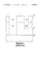
- substrate 100represents a semiconductor substrate and any device layers or structures underlying the oxide layer 101 through which the etch is to be performed.
- silicon nitride layer(Si 3 N 4 ) underlying oxide layer 101.
- silicon nitride layer or nitride layeris used generally to refer to a layer of Si x N y , wherein the ratio x:y may or may not be stoichiometric, as well as to various silicon oxynitride films (Si x O y N z ).
- patterning layer 110which may be a photoresist layer, comprises openings 111 and 112. As can be seen, the diameter of opening 112 is much smaller than that of opening 111.
- the oxide opening under photoresist opening 112will have a much greater aspect ratio due to its small diameter.
- the prior art etch processcauses opening 121 through the oxide layer 101 to be fully etched prior to opening 122.
- this aspect ratio dependencymay be overcome by adjusting the feed gas chemistry, adjusting the operating pressure, increasing the pumping speed to allow for high flow/low pressure operation, and the addition of diluent gases.
- these methods of minimizing the aspect ratio dependencytypically result in a tradeoff between ARDE effects and other characteristics such as etch rate, selectivity, and profile control, for example.
- HDPhigh density plasma
- etch characteristicsare generally believed to be affected by polymer residues which deposit during the etch. For this reason, the fluorine to carbon ration (F/C) in the plasma is considered an important determinant in the etch.
- F/Cfluorine to carbon ration
- a plasma with a high F/C ratiowill have a faster etch rate than a plasma with a low F/C ratio.
- the etch rate as a function of the F/C ratiois typically different for different materials.
- This differenceis used to create a selective etch, by attempting to use a gas mixture which puts the F/C ratio in the plasma at a value that leads to etching at a reasonable rate for one material, and that leads to no etching or polymer deposition for another.
- oxide etchingsee S. Wolf and R. N. Tauber, Silicon Processing for the VLSI Era, Volume 1, pp 539-585 (1986).
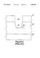
- FIG. 2shows an oxide layer 201 formed on substrate 200, having patterning layer 210 with opening 211 therein.
- Opening 221 in the oxide layer 201is shown during formation.
- high selectivitymay be desired to protect an underlying region of, for example, silicon nitride on the upper surface of substrate 200. It also may be desired to obtain a relativity straight profile.
- the resulting opening 221will have a taper as shown by angle 206. Often, in a prior art etch with acceptable selectivity, the angle 206 is less than 85°. This tradeoff is particularly severe in etches through thick oxide layers. For example, if the process is engineered to allow for a steep wall profile through a thick BPSG layer, the selectivity will be very poor.
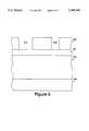
- FIG. 3illustrates the effect of polymer buildup during a typical prior art etch process.
- Polymer buildup along the regions 307 along the sidewalls of opening 321cause the wall profile to be different than a straight etch profile, shown dashed.
- polymer buildup in the region 308 at the center of the bottom of the openingprevents etching of a portion of the nitride layer 302.
- etchingdoes occur around the outer edges.
- the result of the prior art processis poorly controlled wall profile, and non-uniformity of the nitride layer 302 in the bottom of the opening 321.
- changing the gas chemistry and other etch parametersmay be used to improve the etch, but some tradeoffs are inevitable.
- attempts to improve the oxide :nitride selectivityoften lead to non-stable plasma conditions, and involve high polymer chemistries, which in turn leads to dirty reactors requiring extensive maintenance, and particle generation which reduces yields.
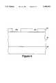
- opening 411 in patterning layer 410is aligned to partially overlie structure 404, which may be, for example, a gate, an interconnect line, or other structure.
- structure 404is covered by silicon nitride etch stop layer 403.
- the opening 421is designed to partially overlie structure 404 to a certain extent. Note that as the etch proceeds, opening 421 will extend to the corner of a gate 430 prior to the completion of the etch to the bottom of the opening at 432.
- the nitride layer 403is removed from structure 404 on the top 430 and side 431, which are exposed to the etch for a significant time before the etch reaches the bottom 432.
- This problemis particularly severe if the opening 411 is misaligned such that the opening in the oxide layer is formed as shown by dashed lines 421a.
- the opening 421aexposes a smaller area of nitride layer 403 than the opening 421. This leads to a reduction in the micro-loading effect, which in turn causes the now reduced area of nitride layer 403 to be etched at a much faster rate.
- etching oxide with reduced ARDE effectwhich exhibit a high oxide to nitride selectivity, and which provide control of wall profile. Further, it is preferable that any such methods do not suffer from severe tradeoffs between and among these and other performance goals such as etch rate, so that highly selective etches with reduced sidewall taper and/or reduced ARDE effects, may be achieved.
- the method or methodsshould enable the formation of openings which lie on or over other structures, such as in a self-aligned contact etch.
- the method or methodsshould allow for increased opening depth, especially in process steps requiring the formation of deep openings of different depths, without an unacceptable sacrifice in performance.
- the method or methodsshould provide the above described etch characteristics without requiring extensive redesign of the process or process tools, unacceptable performance or process maintenance tradeoffs, costly and unproven equipment, or high particle generation.
- a method of etching openings such as contact openings or via openings in an oxide layeris disclosed.
- the method of the present inventionmay be used for a wide variety of etches, including etches with openings having different aspect ratios, over flat structures, over steep topography, and in etches having all of these.
- the ARDE effectis reduced or eliminated, improved oxide:nitride selectivity is achieved, and tradeoffs between selectivity and other performance goals are greatly reduced or eliminated.
- a hard mask layer of, for example, polysiliconis used as a mask for the oxide etch.
- a patterned photoresist layer, exposing regions of the hard mask corresponding to the openings to be formed in the oxide layeris formed on the hard mask.
- an etch of the hard mask in the exposed regionsis then performed. It has been found that the interaction of the photoresist mask, and more particularly it is believed the carbon from the photoresist mask, with the plasma etch chemistry has a dominant effect on the aspect ratio dependency of the etch. Therefore, in one embodiment, the photoresist mask is removed prior to the completion of the oxide etch. The elimination of the photoresist/etch chemistry interaction has been found to greatly reduce or eliminate aspect ratio dependent etch effects. Additionally, the hard mask is found to interact with the etch chemistry to improve the oxide:nitride selectivity. In another embodiment of the present invention, the oxide etch is carried out at an elevated temperature, allowing for increased selectivity without a tradeoff with wall angle.
- Freon 134ais used as an additive to the etchant gas allowing for improved oxide:nitride selectivity.
- the hard mask, Freon 134a, and elevated temperatureare used to perform etches providing a selective oxide :nitride etch over both flat surfaces and corner topography.
- the etchesmay be carried out in two steps. In the case of a thick oxide layer, this allows for a high etch rate, and selectivity, while leaving a uniform nitride underlayer. In one two step etch process, a clean step is performed to remove any built up polymers before proceeding with the second etch step.
- FIG. 1illustrates aspect ratio dependent etching of a prior art oxide etch process.
- FIG. 2illustrates wall profile in a prior art oxide etch process.
- FIG. 3illustrates poor oxide :nitride selectivity in a prior art etch process.
- FIGS. 4illustrates a prior art etch process over a structure.
- FIG. 5is a cross-sectional election view of a structure having a hard mask of one embodiment of the present invention.
- FIG. 6illustrates the structure of FIG. 5 after the etch of the hard mask.
- FIG. 7illustrates the oxide etch performed on the structure of FIG. 6 in an embodiment of the present invention, just prior to completion.
- FIG. 8shows a block diagram of the steps used in the process shown in FIGS. 5-7.
- FIG. 9illustrates the result of an oxide etch in accordance with an embodiment of the present invention.
- FIG. 10Aillustrates the molecular structure of an etchant used in an embodiment of the present invention.
- FIG. 10Billustrates a proposed reaction of the molecule of FIG. 10A.
- FIG. 11shows the result of an oxide etch using a chemistry comprising the etchant shown in FIG. 10.
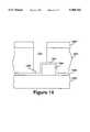
- FIG. 12illustrates a cross-sectional elevation view of a structure on which an oxide etch according to an embodiment of the present invention is to be performed.
- FIG. 13illustrates the structure of FIG. 12 after etching of the hard mask of an embodiment of the present invention.
- FIG. 14illustrates the structure of FIG. 13 after an oxide etch according to an embodiment of the present invention.
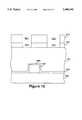
- FIG. 15illustrates a cross-sectional elevation view of a structure to be etched in an embodiment of the present invention.
- FIG. 16shows the structure of FIG. 15 after a first etch step and a clean step.
- FIG. 17illustrates the structure of FIG. 16 after a second etch step.
- a method of etching an oxide layer using a hard maskis disclosed.
- numerous specific detailsare set forth such as specific materials, thicknesses, processing steps, process parameters, etc. in order to provide a thorough understanding of the present invention. It will be obvious, however, to one skilled in the art that these specific details need not be employed to practice the present invention. In other instances, well known materials or methods have not been described in detail in order to avoid unnecessarily obscuring the present invention. Furthermore, in the following discussion, several embodiments of the present invention are illustrated with respect to specific structures, oxide layers, and oxide layer openings.
- each of the methods described hereincan be utilized on a variety of structures and oxide layers, to form any type of opening, and each of the oxide etching methods described herein is not necessarily restricted to the structure and/or oxide layer in conjunction with which is described. Further, any of the methods described herein may be performed as a part of a multistep etch comprising additional etch processes. Several exemplary multistep processes are described below.
- FIGS. 5-7illustrate a structure during fabrication according to a preferred embodiment of the present invention.
- FIG. 8shows a block diagram of the process shown in conjunction with FIGS. 5-7.
- substrate 500having oxide layer 501 thereon is formed, as illustrated in FIG. 5.
- Substrate 500may comprise a semiconductor substrate including device regions, layers, and structures, and may have varying topography underlying oxide layer 501.
- Oxide layer 501may be any type of oxide, doped or undoped, and may be a grown oxide or a deposited oxide deposited by any method such as CVD, sputter deposition, etc. It will be appreciated that oxide layer 501 may be a multilayer structure consisting of several different types of oxide layers.
- oxide layer 501comprises a 10,000 ⁇ BPSG layer, which itself may comprise several sublayers of different dopant concentrations, plus 3000 ⁇ of undoped oxide on top of the BPSG layer.
- the oxide layer 501is disposed on a 900 ⁇ CVD nitride layer comprising the uppermost surface of substrate 500.
- a hard maskis formed on the oxide layer.
- hard mask layer 505is deposited upon oxide layer 501.
- hard mask layer 505comprises polysilicon deposited by, for example, CVD to a thickness in the range of approximately 500-5000 ⁇ .
- hard mask layer 505can be deposited by any well known method, and that other thicknesses may be used. Additionally, it will be appreciated that other types of layers or combination of layers may be used as the hard mask, such as silicon nitride, aluminum, titanium silicide, tungsten, or other refractory metal, etc. For reasons that will be seen, hard mask layer 505 is preferably a non-carbon or very low carbon contributing film.
- opening 515is significantly greater than that of opening 516, so that opening 516 has a much higher aspect ratio. As described earlier, this typically leads to a much slower oxide etch rate in the region of opening 516. However, with use of the hard mask 505 this is avoided in the present invention.
- the structure of FIG. 6is next subjected to an oxide etch in step 805 to form openings in the oxide layer corresponding to hard mask openings 515 and 516. Referring to FIG. 7, openings 521 and 522 in the oxide layer 501 during the etch, at a time just prior to completion of the etch, are shown. As can be seen, the openings 521 and 522 extend approximately the same distance through the oxide layer 501.
- substrate 500may have varying topography, so that the openings through oxide layer 501 extend to varying depths. Therefore, in such a case, even if all openings have the same diameter, there will be varying aspect ratios across the wafer due to the different depths. Additionally there may be both varying depths and varying diameters of openings. In all of these cases, the hard mask of the present invention has been found to reduce or eliminate the aspect ratio dependency of the etch.
- the use of hard mask 505is advantageous in any etch process
- one embodiment of the present inventionis carried out in the LAM 384T Dry Etch System which is an RIE/Triode system.
- the etchis carried out in a flow comprising 2.5 standard cubic centimeters per minute (SCCM) Freon 134a and 10 SCCM CHF 3 (Freon 23).
- SCCMstandard cubic centimeters per minute
- the etchis carried out at 600 watts (W) with a DC bias of approximately 1400 volts (V).
- the etchis performed at a pressure in the range of approximately 10-40 mTorr.
- the lower electrode water coolant temperatureis set at 17° C.
- the upper chamber temperatureis set at 50° C.
- the etchmay be carried out in two steps, with a first portion of the oxide layer etched with resist layer 510 intact, followed by resist strip, and then a high performance final etch step with just the hard mask remaining to define the openings.
- a high etch rate, non-selective etch stepdesigned to etch the undoped oxide layer and some of the doped layer, such that there remains approximately 2000 ⁇ of oxide in the thinnest area of the wafer, is first performed, followed by a second etch step similar to that described above.
- a clean stepmay be performed between the etch steps.
- a photosensitive layer which has been treated to become relatively inert to the plasma chemistrymay be used as the sole masking layer.
- a silylated photoresist layerformed by, for example, a process known as the "DESIRE" process may be used.
- the exposed resist layeris treated with HMDS or a similar compound to impregnate portions of the layer with silicon. See, for example, Pavelchek et al., "Process Techniques For Improving Performance of Positive Tone Silylation" SPIE vol.
- a photosensitive layer treated in this or a similar mannerwhich does not significantly react with the etch chemistry, and therefore does not overwhelm the carbon content of the plasma, may be used in place of the hard mask layer described herein. In this case, there is no need for both a patterning layer and a hard mask layer as described above.
- an existing oxide etch processneed not be reengineered, performed on new equipment, etc., and many of the tradeoffs associated therewith can be avoided or minimized.
- the etchcan be tailored without the problem of carbon from the photoresist overwhelming the etch characteristics.
- embodiments of the present inventionfurther include methods of minimizing the selectivity/wall angle tradeoff, improved oxide:nitride selectivity, improved selectivity in etches requiring openings to extend over corners, and methods of etching deep openings in the oxide layer. The methods of the present invention may be used to achieve the various performance goals as described generally herein, and may be used to improve process latitude.
- the wafer temperatureis controlled by a flow of a coolant such as water through the lower electrode, and/or by a flow of, for example, helium gas to the backside of the wafer. In typical processes, the cooling is carried out such that the wafer reaches a maximum temperature in the range of approximately 60°-80° C.
- the upper temperature limitis constrained by the use of a photoresist patterning layer, since the wafer must be cooled sufficiently to prevent the resist temperature from exceeding the resist reticulation temperature, at which point the resist layer deforms, leading to loss of dimensional control, and potential openings in areas which are designed to remain unetched.
- Typical resistshave a reticulation temperature of approximately 110° C.
- the resist layermay be removed prior to performing the oxide etch. Therefore, in a further embodiment of the present invention the temperature is adjusted (by appropriate adjustment of the backside coolant flow) above the resist reticulation temperature if desired.
- the backside helium pressureis reduced to approximately 2 Torr, which typically results in a helium flow of approximately 1-5 SCCM, as compared with approximately 8 Torr, which typically results in the helium flow of approximately 5-15 SCCM, for a similar process using a resist mask.
- the wafer temperaturecan be expected to reach temperatures of approximately 100°-200° C. or higher.
- the wafer temperatureis maintained at approximately 110°-130° C. Note that this temperature range is above the resist reticulation temperature described above.
- FIG. 9shows an example of opening 921 formed in oxide layer 901, which may be any type of oxide layer, using hard mask 905, which is generally similar to hard mask 505.
- the substrate 900is generally similar to substrate 500, and may comprise many layers, structures, and may have topography underlying the openings to be formed. As before, a plurality of openings may be formed having different diameters and/or different aspect ratios.
- the etchis performed with the above described helium flow and pressure. In one embodiment the etch is performed in a flow comprising approximately 1.5 SCCM Freon 134a and approximately 47 SCCM CHF 3 . The etch is carried out at a power of 600 W, a pressure of 30 mTorr, and a DC bias of approximately 1400 V.
- the lower electrode water coolant temperatureis set at approximately 17° C. and the upper chamber temperature is 50° C.
- the angle 906 using the increased temperatureis greater than 85°. This is in contrast to the angle 206 of FIG. 2. It is believed that the elevated temperature improves the wall angle by preferentially inhibiting polymer formation on the oxide sidewall as compared with the bottom of the opening. In some cases this provides a steep wall angle and an increase in selectivity. It has been found that the profile control is maintained even through layers of different types of oxide, such as doped and undoped, as well as various doping levels.
- the increased temperaturecauses all types of oxides to be less "sticky" than other layers, particularly nitride, so that high etch selectivity of oxide to silicon, silicon nitride, titanium silicide, etc. may be achieved.
- the use of a higher temperature to improve wall profile without selectivity tradeoffis applicable to any process using any chemistry. Because the selectivity is improved or remains the same, at the higher temperature a greater process latitude results. For example, selective etches of relatively thick layers of BPSG, with good profile control may be achieved.
- the temperature increasegenerally increases the etch rate, so that throughput is higher. In addition to this improved wall angle, the embodiment illustrated in FIG. 9 also achieves the earlier described advantages of the hard mask layer.
- Freon 134ahas the formula C 2 H 2 F 4 .
- An illustration of the Freon 134a molecule 1002is shown in FIG. 10A.
- the etchis performed in a mixture comprising Freon 134a, and Freon 23 (CHF 3 ).
- the etchis performed with a Freon 134a flow rate of approximately 1.5 SCCM, a CHF 3 flow rate of approximately 47 SCCM, a pressure in the range of approximately 10-40 mTorr, a power of approximately 400-1200 W, and a DC bias in the range of approximately 1000-2000 V.
- oxide layer 1101 overlying nitride layer 1103 on substrate 1100is shown.
- Substrate 1100is generally similar to the substrates described previously, and oxide layer 1101 is generally similar to oxide layer 501.
- Hard mask layer 1105has been patterned and etched to form an opening 1111 therein. An etch is performed as described above, and opening 1121 is shown during the etch process.
- the oxide sidewalls 1121ahave minimal polymer deposition, while the bottom 1121b has some polymer buildup.
- the Freon 134a of the present inventionallows for such improved selectivity by working in combination with the polysilicon hard mask to reduce free fluorine (F) neutrals and ions, to reduce their concentration in the plasma, thus decreasing the F/C ratio at nitride surfaces as compared to oxide surfaces. This brings the etch into the regime where oxide etching is still at an acceptable rate, while little etching occurs on the nitride. It is further believed that the increased selectivity may result from the presence of a three carbon chain molecule formed by reaction with Freon 134a molecule 1002 with carbon from another source.
- Freon 134aundergoes the reaction shown in FIG. 10B to create the stabilized molecule 1005.
- the molecule 1005may then undergo a reaction with, for example, CHF 3 to form the above mentioned three carbon molecule.
- the improved selectivityhas been found using Freon 134a together with, for example, CHF 3 .
- mixtures of CHF 3 and CH 2 F 2 (Freon 32), mixtures of CHF 3 and CHF 2 CF 3 (Freon 125), and mixtures of CHF 3 and C 2 F 6 (Freon 116)do not exhibit the improved selectivity of Freon 134a, so that it appears the second hydrogen atom on the first carbon atom may be important to the proposed mechanism.
- the improved selectivity of the present inventionadditionally is believed to be achieved in part by the F gettering action of the hard mask, the hard mask 1105 is preferably polysilicon, or some other F reactive film such as silicon nitride, tungsten (W), titanium silicide (TiSi), etc.
- hard mask 1105is additionally preferably a non-carbon or very low carbon content film.
- Freon 134ahas been found to work on a wide variety of different feature sizes, can be employed in a variety of processes and etch tools. Further, the improved selectivity can be achieved with minimal or no tradeoff with other performance goals.
- the selectivity provided by the present inventioncan be achieved without resort to processes having unstable plasma conditions and without resort to high polymer chemistries, thus avoiding the problems of difficult reactor maintenance, particle generation, and reduced wall profile control.
- varying amounts of Freon 134amay be added, depending upon the particular situation.
- Freon 134amay be added such that the Freon 134a flow is in the range of approximately 3-50% of the total flow.
- FIGS. 12-14illustrate a further embodiment of the present invention overcoming this problem.
- hard mask layer 1205is formed on oxide layer 1201.
- oxide layer 1201comprises a 2000 ⁇ undoped TEOS layer on top of a 12000 ⁇ BPSG layer.
- the hard mask 1205is preferably polysilicon or another F gettering material as described in relation to hard mask 1105.
- Photoresist layer 1210has opening layer 1211 which is aligned to form an opening in the oxide which will partially overlie the structure 1204, i.e., the etch must extend over a corner.
- the process step illustrated in FIG. 12may be a self-aligned contact etch.
- hard mask 1205is etched in the region exposed by opening 1211, to form opening 1216.
- photoresist layer 1210is removed.
- an oxide etchis performed through hard mask 1205, utilizing a gas chemistry comprising Freon 134a at high temperature.
- the etchis performed in a flow comprising 10 SCCM CHF3 and 2.5 SCCM Freon 134a, at a power of 600 W.
- the backside helium pressureis 2 Torr.
- Freon 134atogether with the hard mask 1205 increases the oxide :nitride selectivity.
- the use of increased wafer temperatureprovides good wall profile control and provides further improvement in the oxide :nitride selectivity, leading to good nitride layer uniformity on both horizontal and vertical surfaces.
- Hard mask 1205, in addition to improving selectivityalso provides reduced ARDE effects.
- opening 1221is formed in oxide layer 1201, while a uniform portion of nitride layer 1203 remains on structure 1204 and a uniform portion of nitride layer 1202 remains on the bottom portion 1230 of the opening 1221.
- the nitride layers 1202 and 1203may or may not be formed in the same processing step.
- nitride layer 1202 and 1203have a thickness of approximately 700 ⁇ .
- the present inventioncan be used to perform an oxide etch wherein there are openings that overlie corners and openings that overlie flat surfaces. Additionally, since hard mask 1205 minimizes the ARDE effect, the openings may have different aspect ratios from one another. Note that these results are achieved with existing reactor technology, and without requiring substantial reengineering of the etch process.
- the present inventionprovides for an improved process window for an etch over topography and flat surfaces, and of course provides greater process latitude in any type of etch.
- a further embodiment of the present inventionallows for increased etch depth to be achieved without sacrificing etch performance.
- patterning layer 1510 having openings 1511 and 1512is formed on hard mask layer 1505 which has been deposited on oxide layer 1501.
- Oxide layer 1501may be a relatively thick oxide having a depth in the range approximately 5,000-30,000 ⁇ .
- Oxide layer 1501may comprise several layers of one or more different types of oxide layers.
- oxide layer 1501may comprise an uppermost CVD TEOS oxide layer of approximately 3,000 ⁇ , overlying one or more BPSG layers with a total thickness of approximately 10,000 ⁇ -20,000 ⁇ . Typically, it is difficult to etch through such a thick layer completely due to polymer buildup in the bottom of the forming opening.
- an etchis performed through hard mask layer 1505 to form openings 1516 and 1517 shown in FIG. 15.
- a high etch rate oxide etchis performed which is preferably designed to etch one or more layers of the uppermost portion of oxide layer 1501.
- the etchis tailored to etch the undoped layer and some of the doped layer.
- the etchis performed in a flow comprising 70 SCCM CHF 3 and 20 SCCM C 2 F 6 (Freon 116).
- the etchis performed at a power of 600 W, and a pressure of 50 mTorr.
- a helium coolant pressure of 8 Torris used, and the lower electrode water coolant temperature is set a 17° C.
- a polymer removal stepis performed.
- the polymermay be ashed in an oxygen plasma, for example, or a wet chemical etch may be performed.
- a first clean step in an IPC barrel ash systemperformed in a flow of oxygen (O 2 ) at 1.5 Torr, 400 W for 45 minutes is performed followed by a clean in a solution of H 2 SO 4 •H 2 O 2 at 150° C. for 20 minutes.
- the polymer cleanmay be performed using a single step, similar to one of the above described steps. Additionally, it will be appreciated that many similar clean steps may be performed.
- the patterning layer 1510is also removed.
- FIG. 16shows the structure of FIG. 15 after these steps have been performed, and partial openings 1521' and 1522' have been formed. As can be seen, a substantial thickness of oxide layer 1501 has been removed. Additionally, all polymer has been removed from the openings.
- one of the above described etches of the present inventionsuch as that described in conjunction with FIGS. 12-14, comprising Freon 134a, and at high temperature is performed.
- the structure of FIG. 16 after the second etch stepis shown in FIG. 17.
- openings 1521 and 1522extend all the way through oxide layer 1501 to the surface of nitride layer 1502, which remains uniform in the bottom of the opening. Additionally, nitride layer 1503 overlying structure 1504 remains intact.
- the temperature of the etchcan be varied for the desired taper. For example, an angle 1506 of 85°-90° can be achieved by reducing the helium flow and pressure such that the wafer temperature is elevated as described before. Alternatively, normal cooling can be performed so that the angle 1706 has a taper of less than 85° if desired.
Landscapes
- Engineering & Computer Science (AREA)
- Microelectronics & Electronic Packaging (AREA)
- Condensed Matter Physics & Semiconductors (AREA)
- General Physics & Mathematics (AREA)
- Manufacturing & Machinery (AREA)
- Computer Hardware Design (AREA)
- Physics & Mathematics (AREA)
- Power Engineering (AREA)
- Chemical & Material Sciences (AREA)
- Chemical Kinetics & Catalysis (AREA)
- General Chemical & Material Sciences (AREA)
- Inorganic Chemistry (AREA)
- Drying Of Semiconductors (AREA)
Abstract
Description
Claims (63)
Priority Applications (2)
| Application Number | Priority Date | Filing Date | Title |
|---|---|---|---|
| US08/234,478US5468342A (en) | 1994-04-28 | 1994-04-28 | Method of etching an oxide layer |
| US08/351,784US5562801A (en) | 1994-04-28 | 1994-12-07 | Method of etching an oxide layer |
Applications Claiming Priority (1)
| Application Number | Priority Date | Filing Date | Title |
|---|---|---|---|
| US08/234,478US5468342A (en) | 1994-04-28 | 1994-04-28 | Method of etching an oxide layer |
Related Child Applications (1)
| Application Number | Title | Priority Date | Filing Date |
|---|---|---|---|
| US08/351,784Continuation-In-PartUS5562801A (en) | 1994-04-28 | 1994-12-07 | Method of etching an oxide layer |
Publications (1)
| Publication Number | Publication Date |
|---|---|
| US5468342Atrue US5468342A (en) | 1995-11-21 |
Family
ID=22881554
Family Applications (1)
| Application Number | Title | Priority Date | Filing Date |
|---|---|---|---|
| US08/234,478Expired - LifetimeUS5468342A (en) | 1994-04-28 | 1994-04-28 | Method of etching an oxide layer |
Country Status (1)
| Country | Link |
|---|---|
| US (1) | US5468342A (en) |
Cited By (248)
| Publication number | Priority date | Publication date | Assignee | Title |
|---|---|---|---|---|
| US5661083A (en)* | 1996-01-30 | 1997-08-26 | Integrated Device Technology, Inc. | Method for via formation with reduced contact resistance |
| EP0797242A2 (en)* | 1996-03-19 | 1997-09-24 | Siemens Aktiengesellschaft | Etching high aspect contact holes in solid state devices |
| US5672242A (en)* | 1996-01-31 | 1997-09-30 | Integrated Device Technology, Inc. | High selectivity nitride to oxide etch process |
| US5780363A (en)* | 1997-04-04 | 1998-07-14 | International Business Machines Coporation | Etching composition and use thereof |
| US5821169A (en)* | 1996-08-05 | 1998-10-13 | Sharp Microelectronics Technology,Inc. | Hard mask method for transferring a multi-level photoresist pattern |
| US5873977A (en)* | 1994-09-02 | 1999-02-23 | Sharp Kabushiki Kaisha | Dry etching of layer structure oxides |
| US5880037A (en)* | 1992-09-08 | 1999-03-09 | Applied Materials, Inc. | Oxide etch process using a mixture of a fluorine-substituted hydrocarbon and acetylene that provides high selectivity to nitride and is suitable for use on surfaces of uneven topography |
| US5880019A (en)* | 1997-04-17 | 1999-03-09 | Taiwan Semiconductor Manufacturing Company, Ltd. | Insitu contact descum for self-aligned contact process |
| US5886410A (en)* | 1996-06-26 | 1999-03-23 | Intel Corporation | Interconnect structure with hard mask and low dielectric constant materials |
| US5935877A (en)* | 1995-09-01 | 1999-08-10 | Applied Materials, Inc. | Etch process for forming contacts over titanium silicide |
| US5965465A (en)* | 1997-09-18 | 1999-10-12 | International Business Machines Corporation | Etching of silicon nitride |
| US5972722A (en)* | 1998-04-14 | 1999-10-26 | Texas Instruments Incorporated | Adhesion promoting sacrificial etch stop layer in advanced capacitor structures |
| US5976985A (en)* | 1997-08-14 | 1999-11-02 | Micron Technology, Inc. | Processing methods of forming contact openings and integrated circuitry |
| US6001734A (en)* | 1996-09-20 | 1999-12-14 | Nec Corporation | Formation method of contact/ through hole |
| US6016012A (en)* | 1996-11-05 | 2000-01-18 | Cypress Semiconductor Corporation | Thin liner layer providing reduced via resistance |
| US6027861A (en)* | 1998-03-20 | 2000-02-22 | Taiwan Semiconductor Manufacturing Company | VLSIC patterning process |
| US6033996A (en)* | 1997-11-13 | 2000-03-07 | International Business Machines Corporation | Process for removing etching residues, etching mask and silicon nitride and/or silicon dioxide |
| US6080661A (en)* | 1998-05-29 | 2000-06-27 | Philips Electronics North America Corp. | Methods for fabricating gate and diffusion contacts in self-aligned contact processes |
| US6090674A (en)* | 1998-11-09 | 2000-07-18 | Taiwan Semiconductor Manufacturing Company | Method of forming a hole in the sub quarter micron range |
| US6114250A (en)* | 1998-08-17 | 2000-09-05 | Lam Research Corporation | Techniques for etching a low capacitance dielectric layer on a substrate |
| US6114235A (en)* | 1997-09-05 | 2000-09-05 | Advanced Micro Devices, Inc. | Multipurpose cap layer dielectric |
| US6117796A (en)* | 1998-08-13 | 2000-09-12 | International Business Machines Corporation | Removal of silicon oxide |
| US6117791A (en)* | 1998-06-22 | 2000-09-12 | Micron Technology, Inc. | Etchant with selectivity for doped silicon dioxide over undoped silicon dioxide and silicon nitride, processes which employ the etchant, and structures formed thereby |
| US6121098A (en)* | 1998-06-30 | 2000-09-19 | Infineon Technologies North America Corporation | Semiconductor manufacturing method |
| EP1041622A1 (en)* | 1999-04-01 | 2000-10-04 | Sel Semiconductor Energy Laboratory Co., Ltd. | Interconnect structure between conductor layers and fabricating method thereof |
| US6150282A (en)* | 1997-11-13 | 2000-11-21 | International Business Machines Corporation | Selective removal of etching residues |
| US6159833A (en)* | 1999-09-08 | 2000-12-12 | United Microelectronics Corp. | Method of forming a contact hole in a semiconductor wafer |
| US6159844A (en)* | 1998-05-29 | 2000-12-12 | Philips Electronics North America Corp. | Fabrication of gate and diffusion contacts in self-aligned contact process |
| US6162583A (en)* | 1998-03-20 | 2000-12-19 | Industrial Technology Research Institute | Method for making intermetal dielectrics (IMD) on semiconductor integrated circuits using low dielectric constant spin-on polymers |
| US6165375A (en)* | 1997-09-23 | 2000-12-26 | Cypress Semiconductor Corporation | Plasma etching method |
| US6184119B1 (en)* | 1999-03-15 | 2001-02-06 | Vlsi Technology, Inc. | Methods for reducing semiconductor contact resistance |
| US6184150B1 (en)* | 1992-09-08 | 2001-02-06 | Applied Materials Inc. | Oxide etch process with high selectivity to nitride suitable for use on surfaces of uneven topography |
| US6197698B1 (en)* | 1999-06-28 | 2001-03-06 | United Microelectronics Corp. | Method for etching a poly-silicon layer of a semiconductor wafer |
| US6200891B1 (en) | 1998-08-13 | 2001-03-13 | International Business Machines Corporation | Removal of dielectric oxides |
| US6211034B1 (en) | 1997-04-14 | 2001-04-03 | Texas Instruments Incorporated | Metal patterning with adhesive hardmask layer |
| US6232219B1 (en)* | 1998-05-20 | 2001-05-15 | Micron Technology, Inc. | Self-limiting method of reducing contamination in a contact opening, method of making contacts and semiconductor devices therewith, and resulting structures |
| US6271141B2 (en)* | 1999-03-23 | 2001-08-07 | Micron Technology, Inc. | Methods of forming materials over uneven surface topologies, and methods of forming insulative materials over and between conductive lines |
| US6277752B1 (en)* | 1999-06-28 | 2001-08-21 | Taiwan Semiconductor Manufacturing Company | Multiple etch method for forming residue free patterned hard mask layer |
| US6303496B1 (en)* | 1999-04-27 | 2001-10-16 | Cypress Semiconductor Corporation | Methods of filling constrained spaces with insulating materials and/or of forming contact holes and/or contacts in an integrated circuit |
| US6313040B1 (en)* | 1998-09-28 | 2001-11-06 | Stmicroelectronics S.R.L. | Process for the definition of openings in a dielectric layer |
| US6322716B1 (en) | 1999-08-30 | 2001-11-27 | Cypress Semiconductor Corp. | Method for conditioning a plasma etch chamber |
| US20020000423A1 (en)* | 1992-06-15 | 2002-01-03 | Micron Technologies, Inc. | Method for enhancing oxide to nitride selectivity through the use of independent heat control |
| US6337269B1 (en)* | 2001-06-21 | 2002-01-08 | United Microelectronics Corp. | Method of fabricating a dual damascene structure |
| US6348411B1 (en) | 1998-09-03 | 2002-02-19 | Micron Technology, Inc. | Method of making a contact structure |
| US6372634B1 (en) | 1999-06-15 | 2002-04-16 | Cypress Semiconductor Corp. | Plasma etch chemistry and method of improving etch control |
| US6376366B1 (en)* | 2001-05-21 | 2002-04-23 | Taiwan Semiconductor Manufacturing Company | Partial hard mask open process for hard mask dual damascene etch |
| US6399508B1 (en) | 1999-01-12 | 2002-06-04 | Applied Materials, Inc. | Method for metal etch using a dielectric hard mask |
| US6403488B1 (en) | 1998-03-19 | 2002-06-11 | Cypress Semiconductor Corp. | Selective SAC etch process |
| US6458284B1 (en)* | 1999-08-20 | 2002-10-01 | Mitsubishi Denki Kabushiki Kaisha | Method of etching and etch mask |
| US6461963B1 (en)* | 2000-08-30 | 2002-10-08 | Micron Technology, Inc. | Utilization of disappearing silicon hard mask for fabrication of semiconductor structures |
| WO2002097874A1 (en)* | 2001-05-28 | 2002-12-05 | Lnl Technologies Canada Inc. | Method for deep and vertical dry etching of dielectrics |
| US6491042B1 (en)* | 1998-12-07 | 2002-12-10 | Taiwan Semiconductor Manufacturing Company | Post etching treatment process for high density oxide etcher |
| US20020195419A1 (en)* | 1999-06-11 | 2002-12-26 | Edward K. Pavelchek | Antireflective hard mask compositions |
| US20030003244A1 (en)* | 1998-03-20 | 2003-01-02 | Applied Materials, Inc. | Staggered in-situ deposition and etching of a dielectric layer for HDP CVD |
| US6569774B1 (en) | 2000-08-31 | 2003-05-27 | Micron Technology, Inc. | Method to eliminate striations and surface roughness caused by dry etch |
| US20030118948A1 (en)* | 2001-12-21 | 2003-06-26 | Rohit Grover | Method of etching semiconductor material to achieve structure suitable for optics |
| US20030136332A1 (en)* | 2002-01-24 | 2003-07-24 | Applied Materials Inc., A Delaware Corporation | In situ application of etch back for improved deposition into high-aspect-ratio features |
| US6627547B2 (en) | 1996-08-01 | 2003-09-30 | Cypress Semiconductor Corporation | Hot metallization process |
| US6656847B1 (en) | 1999-11-01 | 2003-12-02 | Taiwan Semiconductor Manufacturing Company | Method for etching silicon nitride selective to titanium silicide |
| US6680258B1 (en) | 2002-10-02 | 2004-01-20 | Promos Technologies, Inc. | Method of forming an opening through an insulating layer of a semiconductor device |
| US6693042B1 (en)* | 2000-12-28 | 2004-02-17 | Cypress Semiconductor Corp. | Method for etching a dielectric layer formed upon a barrier layer |
| US6716758B1 (en)* | 1999-08-25 | 2004-04-06 | Micron Technology, Inc. | Aspect ratio controlled etch selectivity using time modulated DC bias voltage |
| US20040079632A1 (en)* | 2002-10-23 | 2004-04-29 | Applied Materials, Inc. | High density plasma CVD process for gapfill into high aspect ratio features |
| US20040079728A1 (en)* | 2002-10-23 | 2004-04-29 | Applied Materials, Inc. | Reactive ion etching for semiconductor device feature topography modification |
| US6734108B1 (en)* | 1999-09-27 | 2004-05-11 | Cypress Semiconductor Corporation | Semiconductor structure and method of making contacts in a semiconductor structure |
| US6756315B1 (en) | 2000-09-29 | 2004-06-29 | Cypress Semiconductor Corporation | Method of forming contact openings |
| US20040251236A1 (en)* | 2003-05-23 | 2004-12-16 | Applied Materials, Inc. | [deposition-selective etch-deposition process for dielectric film gapfill] |
| US6875371B1 (en) | 1998-06-22 | 2005-04-05 | Micron Technology, Inc. | Etchant with selectivity for doped silicon dioxide over undoped silicon dioxide and silicon nitride, processes which employ the etchant, and structures formed thereby |
| US6903031B2 (en) | 2003-09-03 | 2005-06-07 | Applied Materials, Inc. | In-situ-etch-assisted HDP deposition using SiF4 and hydrogen |
| US6908862B2 (en) | 2002-05-03 | 2005-06-21 | Applied Materials, Inc. | HDP-CVD dep/etch/dep process for improved deposition into high aspect ratio features |
| US6929700B2 (en) | 2001-05-11 | 2005-08-16 | Applied Materials, Inc. | Hydrogen assisted undoped silicon oxide deposition process for HDP-CVD |
| US6958112B2 (en) | 2003-05-27 | 2005-10-25 | Applied Materials, Inc. | Methods and systems for high-aspect-ratio gapfill using atomic-oxygen generation |
| US20060086954A1 (en)* | 2000-12-27 | 2006-04-27 | Natarajan Sanjay S | Multi-layer film stack for extinction of substrate reflections during patterning |
| US7052552B2 (en)* | 2000-08-24 | 2006-05-30 | Applied Materials | Gas chemistry cycling to achieve high aspect ratio gapfill with HDP-CVD |
| US20060154494A1 (en)* | 2005-01-08 | 2006-07-13 | Applied Materials, Inc., A Delaware Corporation | High-throughput HDP-CVD processes for advanced gapfill applications |
| US7087536B2 (en) | 2004-09-01 | 2006-08-08 | Applied Materials | Silicon oxide gapfill deposition using liquid precursors |
| US20060292894A1 (en)* | 2005-06-24 | 2006-12-28 | Applied Materials, Inc., | Gapfill using deposition-etch sequence |
| US20070026677A1 (en)* | 2002-10-11 | 2007-02-01 | Lam Research Corporation | Method for plasma etching performance enhancement |
| US7173339B1 (en) | 1998-06-22 | 2007-02-06 | Micron Technology, Inc. | Semiconductor device having a substrate an undoped silicon oxide structure and an overlaying doped silicon oxide structure with a sidewall terminating at the undoped silicon oxide structure |
| US7183227B1 (en) | 2004-07-01 | 2007-02-27 | Applied Materials, Inc. | Use of enhanced turbomolecular pump for gapfill deposition using high flows of low-mass fluent gas |
| US20070057253A1 (en)* | 2005-08-29 | 2007-03-15 | Rohm And Haas Electronic Materials Llc | Antireflective hard mask compositions |
| US7196021B2 (en) | 2001-05-11 | 2007-03-27 | Applied Materials, Inc. | HDP-CVD deposition process for filling high aspect ratio gaps |
| US7205240B2 (en) | 2003-06-04 | 2007-04-17 | Applied Materials, Inc. | HDP-CVD multistep gapfill process |
| US7229931B2 (en) | 2004-06-16 | 2007-06-12 | Applied Materials, Inc. | Oxygen plasma treatment for enhanced HDP-CVD gapfill |
| US20070193973A1 (en)* | 2006-02-17 | 2007-08-23 | Lam Research Corporation | Infinitely selective photoresist mask etch |
| US20080081475A1 (en)* | 2006-09-29 | 2008-04-03 | Hynix Semiconductor Inc. | Method for forming pattern in semiconductor device |
| US7524750B2 (en) | 2006-04-17 | 2009-04-28 | Applied Materials, Inc. | Integrated process modulation (IPM) a novel solution for gapfill with HDP-CVD |
| US20090236311A1 (en)* | 2006-10-30 | 2009-09-24 | Fhr Anlagenbau Gmbh | Method and Apparatus for Structuring Components Made of a Material Composed of Silicon Oxide |
| US7595088B2 (en) | 2003-01-23 | 2009-09-29 | Applied Materials, Inc. | Hydrogen assisted HDP-CVD deposition process for aggressive gap-fill technology |
| US7678715B2 (en) | 2007-12-21 | 2010-03-16 | Applied Materials, Inc. | Low wet etch rate silicon nitride film |
| US7939422B2 (en) | 2006-12-07 | 2011-05-10 | Applied Materials, Inc. | Methods of thin film process |
| US8399360B1 (en) | 2005-11-17 | 2013-03-19 | Cypress Semiconductor Corporation | Process for post contact-etch clean |
| US8497211B2 (en) | 2011-06-24 | 2013-07-30 | Applied Materials, Inc. | Integrated process modulation for PSG gapfill |
| US8679982B2 (en) | 2011-08-26 | 2014-03-25 | Applied Materials, Inc. | Selective suppression of dry-etch rate of materials containing both silicon and oxygen |
| US8679983B2 (en) | 2011-09-01 | 2014-03-25 | Applied Materials, Inc. | Selective suppression of dry-etch rate of materials containing both silicon and nitrogen |
| US8741778B2 (en) | 2010-12-14 | 2014-06-03 | Applied Materials, Inc. | Uniform dry etch in two stages |
| US8765574B2 (en) | 2012-11-09 | 2014-07-01 | Applied Materials, Inc. | Dry etch process |
| US8771536B2 (en) | 2011-08-01 | 2014-07-08 | Applied Materials, Inc. | Dry-etch for silicon-and-carbon-containing films |
| US8771539B2 (en) | 2011-02-22 | 2014-07-08 | Applied Materials, Inc. | Remotely-excited fluorine and water vapor etch |
| US8801952B1 (en) | 2013-03-07 | 2014-08-12 | Applied Materials, Inc. | Conformal oxide dry etch |
| US8808563B2 (en) | 2011-10-07 | 2014-08-19 | Applied Materials, Inc. | Selective etch of silicon by way of metastable hydrogen termination |
| US8895449B1 (en) | 2013-05-16 | 2014-11-25 | Applied Materials, Inc. | Delicate dry clean |
| US8921234B2 (en) | 2012-12-21 | 2014-12-30 | Applied Materials, Inc. | Selective titanium nitride etching |
| US8927390B2 (en) | 2011-09-26 | 2015-01-06 | Applied Materials, Inc. | Intrench profile |
| US8951429B1 (en) | 2013-10-29 | 2015-02-10 | Applied Materials, Inc. | Tungsten oxide processing |
| US8956980B1 (en) | 2013-09-16 | 2015-02-17 | Applied Materials, Inc. | Selective etch of silicon nitride |
| US8969212B2 (en) | 2012-11-20 | 2015-03-03 | Applied Materials, Inc. | Dry-etch selectivity |
| US20150064919A1 (en)* | 2013-09-05 | 2015-03-05 | Applied Materials, Inc. | Aspect ratio dependent etch (arde) lag reduction process by selective oxidation with inert gas sputtering |
| US8975152B2 (en) | 2011-11-08 | 2015-03-10 | Applied Materials, Inc. | Methods of reducing substrate dislocation during gapfill processing |
| US8980763B2 (en) | 2012-11-30 | 2015-03-17 | Applied Materials, Inc. | Dry-etch for selective tungsten removal |
| US8999856B2 (en) | 2011-03-14 | 2015-04-07 | Applied Materials, Inc. | Methods for etch of sin films |
| US9018108B2 (en) | 2013-01-25 | 2015-04-28 | Applied Materials, Inc. | Low shrinkage dielectric films |
| US9023732B2 (en) | 2013-03-15 | 2015-05-05 | Applied Materials, Inc. | Processing systems and methods for halide scavenging |
| US9023734B2 (en) | 2012-09-18 | 2015-05-05 | Applied Materials, Inc. | Radical-component oxide etch |
| US9034770B2 (en) | 2012-09-17 | 2015-05-19 | Applied Materials, Inc. | Differential silicon oxide etch |
| US9040422B2 (en) | 2013-03-05 | 2015-05-26 | Applied Materials, Inc. | Selective titanium nitride removal |
| US9064815B2 (en) | 2011-03-14 | 2015-06-23 | Applied Materials, Inc. | Methods for etch of metal and metal-oxide films |
| US9064816B2 (en) | 2012-11-30 | 2015-06-23 | Applied Materials, Inc. | Dry-etch for selective oxidation removal |
| US9111877B2 (en) | 2012-12-18 | 2015-08-18 | Applied Materials, Inc. | Non-local plasma oxide etch |
| US9114438B2 (en) | 2013-05-21 | 2015-08-25 | Applied Materials, Inc. | Copper residue chamber clean |
| US9117855B2 (en) | 2013-12-04 | 2015-08-25 | Applied Materials, Inc. | Polarity control for remote plasma |
| US9136273B1 (en) | 2014-03-21 | 2015-09-15 | Applied Materials, Inc. | Flash gate air gap |
| US9132436B2 (en) | 2012-09-21 | 2015-09-15 | Applied Materials, Inc. | Chemical control features in wafer process equipment |
| US9159606B1 (en) | 2014-07-31 | 2015-10-13 | Applied Materials, Inc. | Metal air gap |
| US9165786B1 (en) | 2014-08-05 | 2015-10-20 | Applied Materials, Inc. | Integrated oxide and nitride recess for better channel contact in 3D architectures |
| US9190293B2 (en) | 2013-12-18 | 2015-11-17 | Applied Materials, Inc. | Even tungsten etch for high aspect ratio trenches |
| US9236265B2 (en) | 2013-11-04 | 2016-01-12 | Applied Materials, Inc. | Silicon germanium processing |
| US9245762B2 (en) | 2013-12-02 | 2016-01-26 | Applied Materials, Inc. | Procedure for etch rate consistency |
| US9263278B2 (en) | 2013-12-17 | 2016-02-16 | Applied Materials, Inc. | Dopant etch selectivity control |
| US9269590B2 (en) | 2014-04-07 | 2016-02-23 | Applied Materials, Inc. | Spacer formation |
| US9287134B2 (en) | 2014-01-17 | 2016-03-15 | Applied Materials, Inc. | Titanium oxide etch |
| US9287095B2 (en) | 2013-12-17 | 2016-03-15 | Applied Materials, Inc. | Semiconductor system assemblies and methods of operation |
| US9293568B2 (en) | 2014-01-27 | 2016-03-22 | Applied Materials, Inc. | Method of fin patterning |
| US9299575B2 (en) | 2014-03-17 | 2016-03-29 | Applied Materials, Inc. | Gas-phase tungsten etch |
| US9299583B1 (en) | 2014-12-05 | 2016-03-29 | Applied Materials, Inc. | Aluminum oxide selective etch |
| US9299537B2 (en) | 2014-03-20 | 2016-03-29 | Applied Materials, Inc. | Radial waveguide systems and methods for post-match control of microwaves |
| US9299582B2 (en) | 2013-11-12 | 2016-03-29 | Applied Materials, Inc. | Selective etch for metal-containing materials |
| US9299538B2 (en) | 2014-03-20 | 2016-03-29 | Applied Materials, Inc. | Radial waveguide systems and methods for post-match control of microwaves |
| US9309598B2 (en) | 2014-05-28 | 2016-04-12 | Applied Materials, Inc. | Oxide and metal removal |
| US9324576B2 (en) | 2010-05-27 | 2016-04-26 | Applied Materials, Inc. | Selective etch for silicon films |
| US9343272B1 (en) | 2015-01-08 | 2016-05-17 | Applied Materials, Inc. | Self-aligned process |
| US9349605B1 (en) | 2015-08-07 | 2016-05-24 | Applied Materials, Inc. | Oxide etch selectivity systems and methods |
| US9355856B2 (en) | 2014-09-12 | 2016-05-31 | Applied Materials, Inc. | V trench dry etch |
| US9355862B2 (en) | 2014-09-24 | 2016-05-31 | Applied Materials, Inc. | Fluorine-based hardmask removal |
| US9362130B2 (en) | 2013-03-01 | 2016-06-07 | Applied Materials, Inc. | Enhanced etching processes using remote plasma sources |
| US9368364B2 (en) | 2014-09-24 | 2016-06-14 | Applied Materials, Inc. | Silicon etch process with tunable selectivity to SiO2 and other materials |
| US9373517B2 (en) | 2012-08-02 | 2016-06-21 | Applied Materials, Inc. | Semiconductor processing with DC assisted RF power for improved control |
| US9373522B1 (en) | 2015-01-22 | 2016-06-21 | Applied Mateials, Inc. | Titanium nitride removal |
| US9378969B2 (en) | 2014-06-19 | 2016-06-28 | Applied Materials, Inc. | Low temperature gas-phase carbon removal |
| US9378978B2 (en) | 2014-07-31 | 2016-06-28 | Applied Materials, Inc. | Integrated oxide recess and floating gate fin trimming |
| US9385028B2 (en) | 2014-02-03 | 2016-07-05 | Applied Materials, Inc. | Air gap process |
| US9390937B2 (en) | 2012-09-20 | 2016-07-12 | Applied Materials, Inc. | Silicon-carbon-nitride selective etch |
| US9396989B2 (en) | 2014-01-27 | 2016-07-19 | Applied Materials, Inc. | Air gaps between copper lines |
| US9406523B2 (en) | 2014-06-19 | 2016-08-02 | Applied Materials, Inc. | Highly selective doped oxide removal method |
| US9425058B2 (en) | 2014-07-24 | 2016-08-23 | Applied Materials, Inc. | Simplified litho-etch-litho-etch process |
| US9449846B2 (en) | 2015-01-28 | 2016-09-20 | Applied Materials, Inc. | Vertical gate separation |
| US9478432B2 (en) | 2014-09-25 | 2016-10-25 | Applied Materials, Inc. | Silicon oxide selective removal |
| US9493879B2 (en) | 2013-07-12 | 2016-11-15 | Applied Materials, Inc. | Selective sputtering for pattern transfer |
| US9496167B2 (en) | 2014-07-31 | 2016-11-15 | Applied Materials, Inc. | Integrated bit-line airgap formation and gate stack post clean |
| US9499898B2 (en) | 2014-03-03 | 2016-11-22 | Applied Materials, Inc. | Layered thin film heater and method of fabrication |
| US9502258B2 (en) | 2014-12-23 | 2016-11-22 | Applied Materials, Inc. | Anisotropic gap etch |
| US9553102B2 (en) | 2014-08-19 | 2017-01-24 | Applied Materials, Inc. | Tungsten separation |
| US9576809B2 (en) | 2013-11-04 | 2017-02-21 | Applied Materials, Inc. | Etch suppression with germanium |
| US9659753B2 (en) | 2014-08-07 | 2017-05-23 | Applied Materials, Inc. | Grooved insulator to reduce leakage current |
| US20170178914A1 (en)* | 2015-12-21 | 2017-06-22 | Varian Semiconductor Equipment Associates, Inc. | Etch Rate Modulation Through Ion Implantation |
| US9691645B2 (en) | 2015-08-06 | 2017-06-27 | Applied Materials, Inc. | Bolted wafer chuck thermal management systems and methods for wafer processing systems |
| US9721789B1 (en) | 2016-10-04 | 2017-08-01 | Applied Materials, Inc. | Saving ion-damaged spacers |
| US9728437B2 (en) | 2015-02-03 | 2017-08-08 | Applied Materials, Inc. | High temperature chuck for plasma processing systems |
| US9741593B2 (en) | 2015-08-06 | 2017-08-22 | Applied Materials, Inc. | Thermal management systems and methods for wafer processing systems |
| US9768034B1 (en) | 2016-11-11 | 2017-09-19 | Applied Materials, Inc. | Removal methods for high aspect ratio structures |
| US9773648B2 (en) | 2013-08-30 | 2017-09-26 | Applied Materials, Inc. | Dual discharge modes operation for remote plasma |
| US9847289B2 (en) | 2014-05-30 | 2017-12-19 | Applied Materials, Inc. | Protective via cap for improved interconnect performance |
| US9865484B1 (en) | 2016-06-29 | 2018-01-09 | Applied Materials, Inc. | Selective etch using material modification and RF pulsing |
| US9881805B2 (en) | 2015-03-02 | 2018-01-30 | Applied Materials, Inc. | Silicon selective removal |
| US9885117B2 (en) | 2014-03-31 | 2018-02-06 | Applied Materials, Inc. | Conditioned semiconductor system parts |
| US9934942B1 (en) | 2016-10-04 | 2018-04-03 | Applied Materials, Inc. | Chamber with flow-through source |
| US9947549B1 (en) | 2016-10-10 | 2018-04-17 | Applied Materials, Inc. | Cobalt-containing material removal |
| US10026621B2 (en) | 2016-11-14 | 2018-07-17 | Applied Materials, Inc. | SiN spacer profile patterning |
| US10043674B1 (en) | 2017-08-04 | 2018-08-07 | Applied Materials, Inc. | Germanium etching systems and methods |
| US10043684B1 (en) | 2017-02-06 | 2018-08-07 | Applied Materials, Inc. | Self-limiting atomic thermal etching systems and methods |
| US10049891B1 (en) | 2017-05-31 | 2018-08-14 | Applied Materials, Inc. | Selective in situ cobalt residue removal |
| US10062585B2 (en) | 2016-10-04 | 2018-08-28 | Applied Materials, Inc. | Oxygen compatible plasma source |
| US10062579B2 (en) | 2016-10-07 | 2018-08-28 | Applied Materials, Inc. | Selective SiN lateral recess |
| US10062587B2 (en) | 2012-07-18 | 2018-08-28 | Applied Materials, Inc. | Pedestal with multi-zone temperature control and multiple purge capabilities |
| US10062575B2 (en) | 2016-09-09 | 2018-08-28 | Applied Materials, Inc. | Poly directional etch by oxidation |
| US10128086B1 (en) | 2017-10-24 | 2018-11-13 | Applied Materials, Inc. | Silicon pretreatment for nitride removal |
| US10163696B2 (en) | 2016-11-11 | 2018-12-25 | Applied Materials, Inc. | Selective cobalt removal for bottom up gapfill |
| US10170336B1 (en) | 2017-08-04 | 2019-01-01 | Applied Materials, Inc. | Methods for anisotropic control of selective silicon removal |
| US10170282B2 (en) | 2013-03-08 | 2019-01-01 | Applied Materials, Inc. | Insulated semiconductor faceplate designs |
| US10224210B2 (en) | 2014-12-09 | 2019-03-05 | Applied Materials, Inc. | Plasma processing system with direct outlet toroidal plasma source |
| US10242908B2 (en) | 2016-11-14 | 2019-03-26 | Applied Materials, Inc. | Airgap formation with damage-free copper |
| US10256112B1 (en) | 2017-12-08 | 2019-04-09 | Applied Materials, Inc. | Selective tungsten removal |
| US10256079B2 (en) | 2013-02-08 | 2019-04-09 | Applied Materials, Inc. | Semiconductor processing systems having multiple plasma configurations |
| US10283321B2 (en) | 2011-01-18 | 2019-05-07 | Applied Materials, Inc. | Semiconductor processing system and methods using capacitively coupled plasma |
| US10283324B1 (en) | 2017-10-24 | 2019-05-07 | Applied Materials, Inc. | Oxygen treatment for nitride etching |
| US10297458B2 (en) | 2017-08-07 | 2019-05-21 | Applied Materials, Inc. | Process window widening using coated parts in plasma etch processes |
| US10319739B2 (en) | 2017-02-08 | 2019-06-11 | Applied Materials, Inc. | Accommodating imperfectly aligned memory holes |
| US10319649B2 (en) | 2017-04-11 | 2019-06-11 | Applied Materials, Inc. | Optical emission spectroscopy (OES) for remote plasma monitoring |
| US10319600B1 (en) | 2018-03-12 | 2019-06-11 | Applied Materials, Inc. | Thermal silicon etch |
| US10354889B2 (en) | 2017-07-17 | 2019-07-16 | Applied Materials, Inc. | Non-halogen etching of silicon-containing materials |
| US10403507B2 (en) | 2017-02-03 | 2019-09-03 | Applied Materials, Inc. | Shaped etch profile with oxidation |
| US10431429B2 (en) | 2017-02-03 | 2019-10-01 | Applied Materials, Inc. | Systems and methods for radial and azimuthal control of plasma uniformity |
| US10468267B2 (en) | 2017-05-31 | 2019-11-05 | Applied Materials, Inc. | Water-free etching methods |
| US10490418B2 (en) | 2014-10-14 | 2019-11-26 | Applied Materials, Inc. | Systems and methods for internal surface conditioning assessment in plasma processing equipment |
| US10490406B2 (en) | 2018-04-10 | 2019-11-26 | Appled Materials, Inc. | Systems and methods for material breakthrough |
| US10497573B2 (en) | 2018-03-13 | 2019-12-03 | Applied Materials, Inc. | Selective atomic layer etching of semiconductor materials |
| US10504754B2 (en) | 2016-05-19 | 2019-12-10 | Applied Materials, Inc. | Systems and methods for improved semiconductor etching and component protection |
| US10504700B2 (en) | 2015-08-27 | 2019-12-10 | Applied Materials, Inc. | Plasma etching systems and methods with secondary plasma injection |
| US10522371B2 (en) | 2016-05-19 | 2019-12-31 | Applied Materials, Inc. | Systems and methods for improved semiconductor etching and component protection |
| US10541246B2 (en) | 2017-06-26 | 2020-01-21 | Applied Materials, Inc. | 3D flash memory cells which discourage cross-cell electrical tunneling |
| US10541184B2 (en) | 2017-07-11 | 2020-01-21 | Applied Materials, Inc. | Optical emission spectroscopic techniques for monitoring etching |
| US10546729B2 (en) | 2016-10-04 | 2020-01-28 | Applied Materials, Inc. | Dual-channel showerhead with improved profile |
| US10566206B2 (en) | 2016-12-27 | 2020-02-18 | Applied Materials, Inc. | Systems and methods for anisotropic material breakthrough |
| US10573527B2 (en) | 2018-04-06 | 2020-02-25 | Applied Materials, Inc. | Gas-phase selective etching systems and methods |
| US10573496B2 (en) | 2014-12-09 | 2020-02-25 | Applied Materials, Inc. | Direct outlet toroidal plasma source |
| US10593560B2 (en) | 2018-03-01 | 2020-03-17 | Applied Materials, Inc. | Magnetic induction plasma source for semiconductor processes and equipment |
| US10593523B2 (en) | 2014-10-14 | 2020-03-17 | Applied Materials, Inc. | Systems and methods for internal surface conditioning in plasma processing equipment |
| CN110970288A (en)* | 2018-09-28 | 2020-04-07 | 台湾积体电路制造股份有限公司 | Pre-cleaning for contacts |
| US10615047B2 (en) | 2018-02-28 | 2020-04-07 | Applied Materials, Inc. | Systems and methods to form airgaps |
| US10629473B2 (en) | 2016-09-09 | 2020-04-21 | Applied Materials, Inc. | Footing removal for nitride spacer |
| US10672642B2 (en) | 2018-07-24 | 2020-06-02 | Applied Materials, Inc. | Systems and methods for pedestal configuration |
| US10679870B2 (en) | 2018-02-15 | 2020-06-09 | Applied Materials, Inc. | Semiconductor processing chamber multistage mixing apparatus |
| US10699879B2 (en) | 2018-04-17 | 2020-06-30 | Applied Materials, Inc. | Two piece electrode assembly with gap for plasma control |
| US10727080B2 (en) | 2017-07-07 | 2020-07-28 | Applied Materials, Inc. | Tantalum-containing material removal |
| US10755941B2 (en) | 2018-07-06 | 2020-08-25 | Applied Materials, Inc. | Self-limiting selective etching systems and methods |
| US10854426B2 (en) | 2018-01-08 | 2020-12-01 | Applied Materials, Inc. | Metal recess for semiconductor structures |
| US10872778B2 (en) | 2018-07-06 | 2020-12-22 | Applied Materials, Inc. | Systems and methods utilizing solid-phase etchants |
| US10886137B2 (en) | 2018-04-30 | 2021-01-05 | Applied Materials, Inc. | Selective nitride removal |
| US10892198B2 (en) | 2018-09-14 | 2021-01-12 | Applied Materials, Inc. | Systems and methods for improved performance in semiconductor processing |
| US10903054B2 (en) | 2017-12-19 | 2021-01-26 | Applied Materials, Inc. | Multi-zone gas distribution systems and methods |
| US10920320B2 (en) | 2017-06-16 | 2021-02-16 | Applied Materials, Inc. | Plasma health determination in semiconductor substrate processing reactors |
| US10920319B2 (en) | 2019-01-11 | 2021-02-16 | Applied Materials, Inc. | Ceramic showerheads with conductive electrodes |
| US10943834B2 (en) | 2017-03-13 | 2021-03-09 | Applied Materials, Inc. | Replacement contact process |
| US10964512B2 (en) | 2018-02-15 | 2021-03-30 | Applied Materials, Inc. | Semiconductor processing chamber multistage mixing apparatus and methods |
| US11049755B2 (en) | 2018-09-14 | 2021-06-29 | Applied Materials, Inc. | Semiconductor substrate supports with embedded RF shield |
| US11062887B2 (en) | 2018-09-17 | 2021-07-13 | Applied Materials, Inc. | High temperature RF heater pedestals |
| US11121002B2 (en) | 2018-10-24 | 2021-09-14 | Applied Materials, Inc. | Systems and methods for etching metals and metal derivatives |
| US11239061B2 (en) | 2014-11-26 | 2022-02-01 | Applied Materials, Inc. | Methods and systems to enhance process uniformity |
| US11257693B2 (en) | 2015-01-09 | 2022-02-22 | Applied Materials, Inc. | Methods and systems to improve pedestal temperature control |
| US11276590B2 (en) | 2017-05-17 | 2022-03-15 | Applied Materials, Inc. | Multi-zone semiconductor substrate supports |
| US11276559B2 (en) | 2017-05-17 | 2022-03-15 | Applied Materials, Inc. | Semiconductor processing chamber for multiple precursor flow |
| US11328909B2 (en) | 2017-12-22 | 2022-05-10 | Applied Materials, Inc. | Chamber conditioning and removal processes |
| US11417534B2 (en) | 2018-09-21 | 2022-08-16 | Applied Materials, Inc. | Selective material removal |
| US11437242B2 (en) | 2018-11-27 | 2022-09-06 | Applied Materials, Inc. | Selective removal of silicon-containing materials |
| US11594428B2 (en) | 2015-02-03 | 2023-02-28 | Applied Materials, Inc. | Low temperature chuck for plasma processing systems |
| US11682560B2 (en) | 2018-10-11 | 2023-06-20 | Applied Materials, Inc. | Systems and methods for hafnium-containing film removal |
| US11721527B2 (en) | 2019-01-07 | 2023-08-08 | Applied Materials, Inc. | Processing chamber mixing systems |
| US12340979B2 (en) | 2017-05-17 | 2025-06-24 | Applied Materials, Inc. | Semiconductor processing chamber for improved precursor flow |
Citations (9)
| Publication number | Priority date | Publication date | Assignee | Title |
|---|---|---|---|---|
| US4529476A (en)* | 1983-06-01 | 1985-07-16 | Showa Denko K.K. | Gas for selectively etching silicon nitride and process for selectively etching silicon nitride with the gas |
| US4654112A (en)* | 1984-09-26 | 1987-03-31 | Texas Instruments Incorporated | Oxide etch |
| US4758305A (en)* | 1986-03-11 | 1988-07-19 | Texas Instruments Incorporated | Contact etch method |
| US4832789A (en)* | 1988-04-08 | 1989-05-23 | American Telephone And Telegrph Company, At&T Bell Laboratories | Semiconductor devices having multi-level metal interconnects |
| US5091047A (en)* | 1986-09-11 | 1992-02-25 | National Semiconductor Corp. | Plasma etching using a bilayer mask |
| US5240554A (en)* | 1991-01-22 | 1993-08-31 | Kabushiki Kaisha Toshiba | Method of manufacturing semiconductor device |
| US5264076A (en)* | 1992-12-17 | 1993-11-23 | At&T Bell Laboratories | Integrated circuit process using a "hard mask" |
| US5286344A (en)* | 1992-06-15 | 1994-02-15 | Micron Technology, Inc. | Process for selectively etching a layer of silicon dioxide on an underlying stop layer of silicon nitride |
| US5356515A (en)* | 1990-10-19 | 1994-10-18 | Tokyo Electron Limited | Dry etching method |
- 1994
- 1994-04-28USUS08/234,478patent/US5468342A/ennot_activeExpired - Lifetime
Patent Citations (9)
| Publication number | Priority date | Publication date | Assignee | Title |
|---|---|---|---|---|
| US4529476A (en)* | 1983-06-01 | 1985-07-16 | Showa Denko K.K. | Gas for selectively etching silicon nitride and process for selectively etching silicon nitride with the gas |
| US4654112A (en)* | 1984-09-26 | 1987-03-31 | Texas Instruments Incorporated | Oxide etch |
| US4758305A (en)* | 1986-03-11 | 1988-07-19 | Texas Instruments Incorporated | Contact etch method |
| US5091047A (en)* | 1986-09-11 | 1992-02-25 | National Semiconductor Corp. | Plasma etching using a bilayer mask |
| US4832789A (en)* | 1988-04-08 | 1989-05-23 | American Telephone And Telegrph Company, At&T Bell Laboratories | Semiconductor devices having multi-level metal interconnects |
| US5356515A (en)* | 1990-10-19 | 1994-10-18 | Tokyo Electron Limited | Dry etching method |
| US5240554A (en)* | 1991-01-22 | 1993-08-31 | Kabushiki Kaisha Toshiba | Method of manufacturing semiconductor device |
| US5286344A (en)* | 1992-06-15 | 1994-02-15 | Micron Technology, Inc. | Process for selectively etching a layer of silicon dioxide on an underlying stop layer of silicon nitride |
| US5264076A (en)* | 1992-12-17 | 1993-11-23 | At&T Bell Laboratories | Integrated circuit process using a "hard mask" |
Non-Patent Citations (8)
| Title |
|---|
| A. Misaka, K. Harafuji, H. Nakagawa, and M. Kubota, "Loading Phenomena In Dry-Etching Process Using a New Adsorption Model", Semiconductor Research Center, Matsushita Electric Ind. Co., Ltd., IEEE 1993, pp. 35.2.1-35.2.4., IEDM 93-857. |
| A. Misaka, K. Harafuji, H. Nakagawa, and M. Kubota, Loading Phenomena In Dry Etching Process Using a New Adsorption Model , Semiconductor Research Center, Matsushita Electric Ind. Co., Ltd., IEEE 1993, pp. 35.2.1 35.2.4., IEDM 93 857.* |
| C. A. Spence, S. A. MacDonald, and H. Schlosser, "Silylation of Poly(t-BOC) Styrene Resists: Performance and Mechanisms", U. C. Berkeley and IBM Alameden Research Centre, 14 pages. |
| C. A. Spence, S. A. MacDonald, and H. Schlosser, Silylation of Poly(t BOC) Styrene Resists: Performance and Mechanisms , U. C. Berkeley and IBM Alameden Research Centre, 14 pages.* |
| Edward Pavelcheck, Gary Calabrese, Bruce Dudley, Susan Jones, Peter Freeman, John Bohland, and Roger Sinta, "Process Techniques for Improving Performance of Positive Tone Silylation", SPIE vol. 1925, Jan. 1993, pp. 264-269. |
| Edward Pavelcheck, Gary Calabrese, Bruce Dudley, Susan Jones, Peter Freeman, John Bohland, and Roger Sinta, Process Techniques for Improving Performance of Positive Tone Silylation , SPIE vol. 1925, Jan. 1993, pp. 264 269.* |
| T. Fukase, H. Hada, H. Aoki, and T. Kunio, "A Margin-Free Contact Process Using an A1203 Etch-Stop Layer for High Density Devices", Microelectronics Research Laboratories, Nec Corp., IEEE 1992, pp. 33.3.1-33.3.4., IEDM 92-837. |
| T. Fukase, H. Hada, H. Aoki, and T. Kunio, A Margin Free Contact Process Using an A1203 Etch Stop Layer for High Density Devices , Microelectronics Research Laboratories, Nec Corp., IEEE 1992, pp. 33.3.1 33.3.4., IEDM 92 837.* |
Cited By (383)
| Publication number | Priority date | Publication date | Assignee | Title |
|---|---|---|---|---|
| US7049244B2 (en) | 1992-06-15 | 2006-05-23 | Micron Technology, Inc. | Method for enhancing silicon dioxide to silicon nitride selectivity |
| US20020000423A1 (en)* | 1992-06-15 | 2002-01-03 | Micron Technologies, Inc. | Method for enhancing oxide to nitride selectivity through the use of independent heat control |
| US5880037A (en)* | 1992-09-08 | 1999-03-09 | Applied Materials, Inc. | Oxide etch process using a mixture of a fluorine-substituted hydrocarbon and acetylene that provides high selectivity to nitride and is suitable for use on surfaces of uneven topography |
| US6184150B1 (en)* | 1992-09-08 | 2001-02-06 | Applied Materials Inc. | Oxide etch process with high selectivity to nitride suitable for use on surfaces of uneven topography |
| US5873977A (en)* | 1994-09-02 | 1999-02-23 | Sharp Kabushiki Kaisha | Dry etching of layer structure oxides |
| US5935877A (en)* | 1995-09-01 | 1999-08-10 | Applied Materials, Inc. | Etch process for forming contacts over titanium silicide |
| US5661083A (en)* | 1996-01-30 | 1997-08-26 | Integrated Device Technology, Inc. | Method for via formation with reduced contact resistance |
| US5672242A (en)* | 1996-01-31 | 1997-09-30 | Integrated Device Technology, Inc. | High selectivity nitride to oxide etch process |
| EP0797242A2 (en)* | 1996-03-19 | 1997-09-24 | Siemens Aktiengesellschaft | Etching high aspect contact holes in solid state devices |
| US6008121A (en)* | 1996-03-19 | 1999-12-28 | Siemens Aktiengesellschaft | Etching high aspect contact holes in solid state devices |
| US5886410A (en)* | 1996-06-26 | 1999-03-23 | Intel Corporation | Interconnect structure with hard mask and low dielectric constant materials |
| US6027995A (en)* | 1996-06-26 | 2000-02-22 | Intel Corporation | Method for fabricating an interconnect structure with hard mask and low dielectric constant materials |
| US6627547B2 (en) | 1996-08-01 | 2003-09-30 | Cypress Semiconductor Corporation | Hot metallization process |
| US5821169A (en)* | 1996-08-05 | 1998-10-13 | Sharp Microelectronics Technology,Inc. | Hard mask method for transferring a multi-level photoresist pattern |
| US6001734A (en)* | 1996-09-20 | 1999-12-14 | Nec Corporation | Formation method of contact/ through hole |
| US6016012A (en)* | 1996-11-05 | 2000-01-18 | Cypress Semiconductor Corporation | Thin liner layer providing reduced via resistance |
| US5780363A (en)* | 1997-04-04 | 1998-07-14 | International Business Machines Coporation | Etching composition and use thereof |
| US6211034B1 (en) | 1997-04-14 | 2001-04-03 | Texas Instruments Incorporated | Metal patterning with adhesive hardmask layer |
| US5880019A (en)* | 1997-04-17 | 1999-03-09 | Taiwan Semiconductor Manufacturing Company, Ltd. | Insitu contact descum for self-aligned contact process |
| US5986347A (en)* | 1997-08-14 | 1999-11-16 | Micron Technology, Inc. | Processing methods of forming contact openings and integrated circuitry |
| US5976985A (en)* | 1997-08-14 | 1999-11-02 | Micron Technology, Inc. | Processing methods of forming contact openings and integrated circuitry |
| US6114235A (en)* | 1997-09-05 | 2000-09-05 | Advanced Micro Devices, Inc. | Multipurpose cap layer dielectric |
| US6066267A (en)* | 1997-09-18 | 2000-05-23 | International Business Machines Corporation | Etching of silicon nitride |
| US5965465A (en)* | 1997-09-18 | 1999-10-12 | International Business Machines Corporation | Etching of silicon nitride |
| US6406640B1 (en) | 1997-09-23 | 2002-06-18 | Cypress Semiconductor Corporation | Plasma etching method |
| US6165375A (en)* | 1997-09-23 | 2000-12-26 | Cypress Semiconductor Corporation | Plasma etching method |
| US6150282A (en)* | 1997-11-13 | 2000-11-21 | International Business Machines Corporation | Selective removal of etching residues |
| US6033996A (en)* | 1997-11-13 | 2000-03-07 | International Business Machines Corporation | Process for removing etching residues, etching mask and silicon nitride and/or silicon dioxide |
| US6403488B1 (en) | 1998-03-19 | 2002-06-11 | Cypress Semiconductor Corp. | Selective SAC etch process |
| US20050032382A1 (en)* | 1998-03-20 | 2005-02-10 | Applied Materials, Inc. | Staggered in-situ deposition and etching of a dielectric layer for HDP CVD |
| US6821577B2 (en) | 1998-03-20 | 2004-11-23 | Applied Materials, Inc. | Staggered in-situ deposition and etching of a dielectric layer for HDP CVD |
| US20030003244A1 (en)* | 1998-03-20 | 2003-01-02 | Applied Materials, Inc. | Staggered in-situ deposition and etching of a dielectric layer for HDP CVD |
| US20070071908A1 (en)* | 1998-03-20 | 2007-03-29 | Applied Materials, Inc. | Staggered in-situ deposition and etching of a dielectric layer for HDP-CVD |
| US6162583A (en)* | 1998-03-20 | 2000-12-19 | Industrial Technology Research Institute | Method for making intermetal dielectrics (IMD) on semiconductor integrated circuits using low dielectric constant spin-on polymers |
| US7455893B2 (en) | 1998-03-20 | 2008-11-25 | Applied Materials, Inc. | Staggered in-situ deposition and etching of a dielectric layer for HDP-CVD |
| US7132134B2 (en) | 1998-03-20 | 2006-11-07 | Applied Materials, Inc. | Staggered in-situ deposition and etching of a dielectric layer for HDP CVD |
| US6027861A (en)* | 1998-03-20 | 2000-02-22 | Taiwan Semiconductor Manufacturing Company | VLSIC patterning process |
| US5972722A (en)* | 1998-04-14 | 1999-10-26 | Texas Instruments Incorporated | Adhesion promoting sacrificial etch stop layer in advanced capacitor structures |
| US6232219B1 (en)* | 1998-05-20 | 2001-05-15 | Micron Technology, Inc. | Self-limiting method of reducing contamination in a contact opening, method of making contacts and semiconductor devices therewith, and resulting structures |
| US6400029B1 (en) | 1998-05-20 | 2002-06-04 | Micron Technology, Inc. | Self-limiting method of reducing contamination in a contact opening, method of making contacts and semiconductor devices therewith, and resulting structures |
| US6159844A (en)* | 1998-05-29 | 2000-12-12 | Philips Electronics North America Corp. | Fabrication of gate and diffusion contacts in self-aligned contact process |
| US6080661A (en)* | 1998-05-29 | 2000-06-27 | Philips Electronics North America Corp. | Methods for fabricating gate and diffusion contacts in self-aligned contact processes |
| US6537922B1 (en) | 1998-06-22 | 2003-03-25 | Micron Technology, Inc. | Etchant with selectivity for doped silicon dioxide over undoped silicon dioxide and silicon nitride, processes which employ the etchant, and structures formed thereby |
| US7173339B1 (en) | 1998-06-22 | 2007-02-06 | Micron Technology, Inc. | Semiconductor device having a substrate an undoped silicon oxide structure and an overlaying doped silicon oxide structure with a sidewall terminating at the undoped silicon oxide structure |
| US7319075B2 (en) | 1998-06-22 | 2008-01-15 | Micron Technology, Inc. | Etchant with selectivity for doped silicon dioxide over undoped silicon dioxide and silicon nitride, processes which employ the etchant, and structures formed thereby |
| US6121671A (en)* | 1998-06-22 | 2000-09-19 | Micron Technology, Inc. | Semiconductor device having a substrate, an undoped silicon oxide structure, and an overlying doped silicon oxide structure with a side wall terminating at the undoped silicon oxide structure |
| US6117791A (en)* | 1998-06-22 | 2000-09-12 | Micron Technology, Inc. | Etchant with selectivity for doped silicon dioxide over undoped silicon dioxide and silicon nitride, processes which employ the etchant, and structures formed thereby |
| US6875371B1 (en) | 1998-06-22 | 2005-04-05 | Micron Technology, Inc. | Etchant with selectivity for doped silicon dioxide over undoped silicon dioxide and silicon nitride, processes which employ the etchant, and structures formed thereby |
| US20030203639A1 (en)* | 1998-06-22 | 2003-10-30 | Kei-Yu Ko | Etchant with selectivity for doped silicon dioxide over undoped silicon dioxide and silicon nitride, processes which employ the etchant, and structures formed thereby |
| US6121098A (en)* | 1998-06-30 | 2000-09-19 | Infineon Technologies North America Corporation | Semiconductor manufacturing method |
| US6200891B1 (en) | 1998-08-13 | 2001-03-13 | International Business Machines Corporation | Removal of dielectric oxides |
| US6117796A (en)* | 1998-08-13 | 2000-09-12 | International Business Machines Corporation | Removal of silicon oxide |
| US6114250A (en)* | 1998-08-17 | 2000-09-05 | Lam Research Corporation | Techniques for etching a low capacitance dielectric layer on a substrate |
| US6740916B1 (en) | 1998-09-03 | 2004-05-25 | Micron Technology, Inc. | Contact structure for integrated circuit devices |
| US8680595B2 (en) | 1998-09-03 | 2014-03-25 | Micron Technology, Inc. | Sleeve insulators and semiconductor device including the same |
| US7968403B2 (en) | 1998-09-03 | 2011-06-28 | Micron Technology, Inc. | Method of fabricating a sleeve insulator for a contact structure |
| US7115506B2 (en) | 1998-09-03 | 2006-10-03 | Micron Technology, Inc. | Method of making a contact structure |
| US20070004199A1 (en)* | 1998-09-03 | 2007-01-04 | Ireland Philip J | Method of making a contact structure |
| US6348411B1 (en) | 1998-09-03 | 2002-02-19 | Micron Technology, Inc. | Method of making a contact structure |
| US6313040B1 (en)* | 1998-09-28 | 2001-11-06 | Stmicroelectronics S.R.L. | Process for the definition of openings in a dielectric layer |
| US6090674A (en)* | 1998-11-09 | 2000-07-18 | Taiwan Semiconductor Manufacturing Company | Method of forming a hole in the sub quarter micron range |
| US6491042B1 (en)* | 1998-12-07 | 2002-12-10 | Taiwan Semiconductor Manufacturing Company | Post etching treatment process for high density oxide etcher |
| US6399508B1 (en) | 1999-01-12 | 2002-06-04 | Applied Materials, Inc. | Method for metal etch using a dielectric hard mask |
| US6383918B1 (en)* | 1999-03-15 | 2002-05-07 | Philips Electronics | Method for reducing semiconductor contact resistance |
| US6184119B1 (en)* | 1999-03-15 | 2001-02-06 | Vlsi Technology, Inc. | Methods for reducing semiconductor contact resistance |
| US6271141B2 (en)* | 1999-03-23 | 2001-08-07 | Micron Technology, Inc. | Methods of forming materials over uneven surface topologies, and methods of forming insulative materials over and between conductive lines |
| US7335964B2 (en) | 1999-03-23 | 2008-02-26 | Werner Juengling | Semiconductor structures |
| US6479388B2 (en) | 1999-03-23 | 2002-11-12 | Micron Technology, Inc. | Methods of forming materials over uneven surface topologies, and methods of forming insulative materials over and between conductive lines |
| US6890858B2 (en) | 1999-03-23 | 2005-05-10 | Micron Technology, Inc. | Methods of forming materials over uneven surface topologies, and methods of forming insulative materials over and between conductive lines |
| US20050206003A1 (en)* | 1999-03-23 | 2005-09-22 | Werner Juengling | Methods of forming materials over uneven surface topologies, and methods of forming insulative materials over and between conductive lines |
| US6861670B1 (en) | 1999-04-01 | 2005-03-01 | Semiconductor Energy Laboratory Co., Ltd. | Semiconductor device having multi-layer wiring |
| US20050098894A1 (en)* | 1999-04-01 | 2005-05-12 | Semiconductor Energy Laboratory Co., Ltd. | Semiconductor device and the fabricating method thereof |
| EP1041622A1 (en)* | 1999-04-01 | 2000-10-04 | Sel Semiconductor Energy Laboratory Co., Ltd. | Interconnect structure between conductor layers and fabricating method thereof |
| US6303496B1 (en)* | 1999-04-27 | 2001-10-16 | Cypress Semiconductor Corporation | Methods of filling constrained spaces with insulating materials and/or of forming contact holes and/or contacts in an integrated circuit |
| US20020195419A1 (en)* | 1999-06-11 | 2002-12-26 | Edward K. Pavelchek | Antireflective hard mask compositions |
| US7018717B2 (en) | 1999-06-11 | 2006-03-28 | Shipley Company, L.L.C. | Antireflective hard mask compositions |
| US6890448B2 (en) | 1999-06-11 | 2005-05-10 | Shipley Company, L.L.C. | Antireflective hard mask compositions |
| US20030209515A1 (en)* | 1999-06-11 | 2003-11-13 | Shipley Company, L.L.C. | Antireflective hard mask compositions |
| US6372634B1 (en) | 1999-06-15 | 2002-04-16 | Cypress Semiconductor Corp. | Plasma etch chemistry and method of improving etch control |
| US6197698B1 (en)* | 1999-06-28 | 2001-03-06 | United Microelectronics Corp. | Method for etching a poly-silicon layer of a semiconductor wafer |
| US6277752B1 (en)* | 1999-06-28 | 2001-08-21 | Taiwan Semiconductor Manufacturing Company | Multiple etch method for forming residue free patterned hard mask layer |
| US6458284B1 (en)* | 1999-08-20 | 2002-10-01 | Mitsubishi Denki Kabushiki Kaisha | Method of etching and etch mask |
| US6716758B1 (en)* | 1999-08-25 | 2004-04-06 | Micron Technology, Inc. | Aspect ratio controlled etch selectivity using time modulated DC bias voltage |
| US20040161941A1 (en)* | 1999-08-25 | 2004-08-19 | Donohoe Kevin G. | Aspect ratio controlled etch selectivity using time modulated DC bias voltage |
| US20060105577A1 (en)* | 1999-08-25 | 2006-05-18 | Donohoe Kevin G | Aspect ratio controlled etch selectivity using time modulated DC bias voltage |
| US6322716B1 (en) | 1999-08-30 | 2001-11-27 | Cypress Semiconductor Corp. | Method for conditioning a plasma etch chamber |
| US6159833A (en)* | 1999-09-08 | 2000-12-12 | United Microelectronics Corp. | Method of forming a contact hole in a semiconductor wafer |
| US6734108B1 (en)* | 1999-09-27 | 2004-05-11 | Cypress Semiconductor Corporation | Semiconductor structure and method of making contacts in a semiconductor structure |
| US6656847B1 (en) | 1999-11-01 | 2003-12-02 | Taiwan Semiconductor Manufacturing Company | Method for etching silicon nitride selective to titanium silicide |
| US7052552B2 (en)* | 2000-08-24 | 2006-05-30 | Applied Materials | Gas chemistry cycling to achieve high aspect ratio gapfill with HDP-CVD |
| US6461963B1 (en)* | 2000-08-30 | 2002-10-08 | Micron Technology, Inc. | Utilization of disappearing silicon hard mask for fabrication of semiconductor structures |
| US6787472B2 (en) | 2000-08-30 | 2004-09-07 | Micron Technology, Inc. | Utilization of disappearing silicon hard mask for fabrication of semiconductor structures |
| US6689693B2 (en) | 2000-08-30 | 2004-02-10 | Micron Technology, Inc. | Methods for utilization of disappearing silicon hard mask for fabrication of semiconductor structures |
| US6534408B2 (en)* | 2000-08-30 | 2003-03-18 | Micron Technology, Inc. | Utilization of disappearing silicon hard mask for fabrication of semiconductor structures |
| US20030162395A1 (en)* | 2000-08-31 | 2003-08-28 | Micron Technology, Inc. | Method to eliminate striations and surface roughness caused by dry etch |
| US7153779B2 (en) | 2000-08-31 | 2006-12-26 | Micron Technology, Inc. | Method to eliminate striations and surface roughness caused by dry etch |
| US6569774B1 (en) | 2000-08-31 | 2003-05-27 | Micron Technology, Inc. | Method to eliminate striations and surface roughness caused by dry etch |
| US6756315B1 (en) | 2000-09-29 | 2004-06-29 | Cypress Semiconductor Corporation | Method of forming contact openings |
| US20060094251A1 (en)* | 2000-12-27 | 2006-05-04 | Natarajan Sanjay S | Multi-layer film stack for extinction of substrate reflections during patterning |
| US7172960B2 (en)* | 2000-12-27 | 2007-02-06 | Intel Corporation | Multi-layer film stack for extinction of substrate reflections during patterning |
| US7291552B2 (en) | 2000-12-27 | 2007-11-06 | Intel Corporation | Multi-layer film stack for extinction of substrate reflections during patterning |
| US20060086954A1 (en)* | 2000-12-27 | 2006-04-27 | Natarajan Sanjay S | Multi-layer film stack for extinction of substrate reflections during patterning |
| US6693042B1 (en)* | 2000-12-28 | 2004-02-17 | Cypress Semiconductor Corp. | Method for etching a dielectric layer formed upon a barrier layer |
| US7196021B2 (en) | 2001-05-11 | 2007-03-27 | Applied Materials, Inc. | HDP-CVD deposition process for filling high aspect ratio gaps |
| US6929700B2 (en) | 2001-05-11 | 2005-08-16 | Applied Materials, Inc. | Hydrogen assisted undoped silicon oxide deposition process for HDP-CVD |
| US6376366B1 (en)* | 2001-05-21 | 2002-04-23 | Taiwan Semiconductor Manufacturing Company | Partial hard mask open process for hard mask dual damascene etch |
| WO2002097874A1 (en)* | 2001-05-28 | 2002-12-05 | Lnl Technologies Canada Inc. | Method for deep and vertical dry etching of dielectrics |
| US6337269B1 (en)* | 2001-06-21 | 2002-01-08 | United Microelectronics Corp. | Method of fabricating a dual damascene structure |
| US20030118948A1 (en)* | 2001-12-21 | 2003-06-26 | Rohit Grover | Method of etching semiconductor material to achieve structure suitable for optics |
| US20050124166A1 (en)* | 2002-01-24 | 2005-06-09 | Applied Materials, Inc. | In situ application of etch back for improved deposition into high-aspect-ratio features |
| US6869880B2 (en) | 2002-01-24 | 2005-03-22 | Applied Materials, Inc. | In situ application of etch back for improved deposition into high-aspect-ratio features |
| US7399707B2 (en) | 2002-01-24 | 2008-07-15 | Applied Materials, Inc. | In situ application of etch back for improved deposition into high-aspect-ratio features |
| US20030136332A1 (en)* | 2002-01-24 | 2003-07-24 | Applied Materials Inc., A Delaware Corporation | In situ application of etch back for improved deposition into high-aspect-ratio features |
| US6908862B2 (en) | 2002-05-03 | 2005-06-21 | Applied Materials, Inc. | HDP-CVD dep/etch/dep process for improved deposition into high aspect ratio features |
| US6680258B1 (en) | 2002-10-02 | 2004-01-20 | Promos Technologies, Inc. | Method of forming an opening through an insulating layer of a semiconductor device |
| US7977390B2 (en) | 2002-10-11 | 2011-07-12 | Lam Research Corporation | Method for plasma etching performance enhancement |
| US20070026677A1 (en)* | 2002-10-11 | 2007-02-01 | Lam Research Corporation | Method for plasma etching performance enhancement |
| US7628897B2 (en) | 2002-10-23 | 2009-12-08 | Applied Materials, Inc. | Reactive ion etching for semiconductor device feature topography modification |
| US6802944B2 (en) | 2002-10-23 | 2004-10-12 | Applied Materials, Inc. | High density plasma CVD process for gapfill into high aspect ratio features |
| US20040079632A1 (en)* | 2002-10-23 | 2004-04-29 | Applied Materials, Inc. | High density plasma CVD process for gapfill into high aspect ratio features |
| US20040079728A1 (en)* | 2002-10-23 | 2004-04-29 | Applied Materials, Inc. | Reactive ion etching for semiconductor device feature topography modification |
| US7595088B2 (en) | 2003-01-23 | 2009-09-29 | Applied Materials, Inc. | Hydrogen assisted HDP-CVD deposition process for aggressive gap-fill technology |
| US20060228886A1 (en)* | 2003-05-23 | 2006-10-12 | Applied Materials, Inc. | Deposition-selective etch-deposition process for dielectric film gapfill |
| US7799698B2 (en) | 2003-05-23 | 2010-09-21 | Applied Materials, Inc. | Deposition-selective etch-deposition process for dielectric film gapfill |
| US7691753B2 (en) | 2003-05-23 | 2010-04-06 | Applied Materials, Inc. | Deposition-selective etch-deposition process for dielectric film gapfill |
| US20060286764A1 (en)* | 2003-05-23 | 2006-12-21 | Applied Materials, Inc. | Deposition-selective etch-deposition process for dielectric film gapfill |
| US20040251236A1 (en)* | 2003-05-23 | 2004-12-16 | Applied Materials, Inc. | [deposition-selective etch-deposition process for dielectric film gapfill] |
| US7081414B2 (en) | 2003-05-23 | 2006-07-25 | Applied Materials, Inc. | Deposition-selective etch-deposition process for dielectric film gapfill |
| US6958112B2 (en) | 2003-05-27 | 2005-10-25 | Applied Materials, Inc. | Methods and systems for high-aspect-ratio gapfill using atomic-oxygen generation |
| US7205240B2 (en) | 2003-06-04 | 2007-04-17 | Applied Materials, Inc. | HDP-CVD multistep gapfill process |
| US7049211B2 (en) | 2003-09-03 | 2006-05-23 | Applied Materials | In-situ-etch-assisted HDP deposition using SiF4 |
| US6903031B2 (en) | 2003-09-03 | 2005-06-07 | Applied Materials, Inc. | In-situ-etch-assisted HDP deposition using SiF4 and hydrogen |
| US7229931B2 (en) | 2004-06-16 | 2007-06-12 | Applied Materials, Inc. | Oxygen plasma treatment for enhanced HDP-CVD gapfill |
| US7183227B1 (en) | 2004-07-01 | 2007-02-27 | Applied Materials, Inc. | Use of enhanced turbomolecular pump for gapfill deposition using high flows of low-mass fluent gas |
| US7087536B2 (en) | 2004-09-01 | 2006-08-08 | Applied Materials | Silicon oxide gapfill deposition using liquid precursors |
| US20060154494A1 (en)* | 2005-01-08 | 2006-07-13 | Applied Materials, Inc., A Delaware Corporation | High-throughput HDP-CVD processes for advanced gapfill applications |
| US8414747B2 (en) | 2005-01-08 | 2013-04-09 | Applied Materials, Inc. | High-throughput HDP-CVD processes for advanced gapfill applications |
| US7329586B2 (en) | 2005-06-24 | 2008-02-12 | Applied Materials, Inc. | Gapfill using deposition-etch sequence |
| US20060292894A1 (en)* | 2005-06-24 | 2006-12-28 | Applied Materials, Inc., | Gapfill using deposition-etch sequence |
| US7605439B2 (en) | 2005-08-29 | 2009-10-20 | Rohm And Haas Electronic Materials Llc | Antireflective hard mask compositions |
| US20070057253A1 (en)* | 2005-08-29 | 2007-03-15 | Rohm And Haas Electronic Materials Llc | Antireflective hard mask compositions |
| US8399360B1 (en) | 2005-11-17 | 2013-03-19 | Cypress Semiconductor Corporation | Process for post contact-etch clean |
| US20070193973A1 (en)* | 2006-02-17 | 2007-08-23 | Lam Research Corporation | Infinitely selective photoresist mask etch |
| US7910489B2 (en)* | 2006-02-17 | 2011-03-22 | Lam Research Corporation | Infinitely selective photoresist mask etch |
| US7524750B2 (en) | 2006-04-17 | 2009-04-28 | Applied Materials, Inc. | Integrated process modulation (IPM) a novel solution for gapfill with HDP-CVD |
| US20080081475A1 (en)* | 2006-09-29 | 2008-04-03 | Hynix Semiconductor Inc. | Method for forming pattern in semiconductor device |
| US8652341B2 (en)* | 2006-10-30 | 2014-02-18 | Fhr Anlagenbau Gmbh | Method and apparatus for structuring components made of a material composed of silicon oxide |
| US20090236311A1 (en)* | 2006-10-30 | 2009-09-24 | Fhr Anlagenbau Gmbh | Method and Apparatus for Structuring Components Made of a Material Composed of Silicon Oxide |
| US7939422B2 (en) | 2006-12-07 | 2011-05-10 | Applied Materials, Inc. | Methods of thin film process |
| US7678715B2 (en) | 2007-12-21 | 2010-03-16 | Applied Materials, Inc. | Low wet etch rate silicon nitride film |
| US9754800B2 (en) | 2010-05-27 | 2017-09-05 | Applied Materials, Inc. | Selective etch for silicon films |
| US9324576B2 (en) | 2010-05-27 | 2016-04-26 | Applied Materials, Inc. | Selective etch for silicon films |
| US8741778B2 (en) | 2010-12-14 | 2014-06-03 | Applied Materials, Inc. | Uniform dry etch in two stages |
| US10283321B2 (en) | 2011-01-18 | 2019-05-07 | Applied Materials, Inc. | Semiconductor processing system and methods using capacitively coupled plasma |
| US8771539B2 (en) | 2011-02-22 | 2014-07-08 | Applied Materials, Inc. | Remotely-excited fluorine and water vapor etch |
| US8999856B2 (en) | 2011-03-14 | 2015-04-07 | Applied Materials, Inc. | Methods for etch of sin films |
| US10062578B2 (en) | 2011-03-14 | 2018-08-28 | Applied Materials, Inc. | Methods for etch of metal and metal-oxide films |
| US9842744B2 (en) | 2011-03-14 | 2017-12-12 | Applied Materials, Inc. | Methods for etch of SiN films |
| US9064815B2 (en) | 2011-03-14 | 2015-06-23 | Applied Materials, Inc. | Methods for etch of metal and metal-oxide films |
| US8497211B2 (en) | 2011-06-24 | 2013-07-30 | Applied Materials, Inc. | Integrated process modulation for PSG gapfill |
| US8771536B2 (en) | 2011-08-01 | 2014-07-08 | Applied Materials, Inc. | Dry-etch for silicon-and-carbon-containing films |
| US9236266B2 (en) | 2011-08-01 | 2016-01-12 | Applied Materials, Inc. | Dry-etch for silicon-and-carbon-containing films |
| US8679982B2 (en) | 2011-08-26 | 2014-03-25 | Applied Materials, Inc. | Selective suppression of dry-etch rate of materials containing both silicon and oxygen |
| US8679983B2 (en) | 2011-09-01 | 2014-03-25 | Applied Materials, Inc. | Selective suppression of dry-etch rate of materials containing both silicon and nitrogen |
| US8927390B2 (en) | 2011-09-26 | 2015-01-06 | Applied Materials, Inc. | Intrench profile |
| US9012302B2 (en) | 2011-09-26 | 2015-04-21 | Applied Materials, Inc. | Intrench profile |
| US8808563B2 (en) | 2011-10-07 | 2014-08-19 | Applied Materials, Inc. | Selective etch of silicon by way of metastable hydrogen termination |
| US9418858B2 (en) | 2011-10-07 | 2016-08-16 | Applied Materials, Inc. | Selective etch of silicon by way of metastable hydrogen termination |
| US8975152B2 (en) | 2011-11-08 | 2015-03-10 | Applied Materials, Inc. | Methods of reducing substrate dislocation during gapfill processing |
| US10062587B2 (en) | 2012-07-18 | 2018-08-28 | Applied Materials, Inc. | Pedestal with multi-zone temperature control and multiple purge capabilities |
| US10032606B2 (en) | 2012-08-02 | 2018-07-24 | Applied Materials, Inc. | Semiconductor processing with DC assisted RF power for improved control |
| US9373517B2 (en) | 2012-08-02 | 2016-06-21 | Applied Materials, Inc. | Semiconductor processing with DC assisted RF power for improved control |
| US9887096B2 (en) | 2012-09-17 | 2018-02-06 | Applied Materials, Inc. | Differential silicon oxide etch |
| US9034770B2 (en) | 2012-09-17 | 2015-05-19 | Applied Materials, Inc. | Differential silicon oxide etch |
| US9437451B2 (en) | 2012-09-18 | 2016-09-06 | Applied Materials, Inc. | Radical-component oxide etch |
| US9023734B2 (en) | 2012-09-18 | 2015-05-05 | Applied Materials, Inc. | Radical-component oxide etch |
| US9390937B2 (en) | 2012-09-20 | 2016-07-12 | Applied Materials, Inc. | Silicon-carbon-nitride selective etch |
| US11264213B2 (en) | 2012-09-21 | 2022-03-01 | Applied Materials, Inc. | Chemical control features in wafer process equipment |
| US9978564B2 (en) | 2012-09-21 | 2018-05-22 | Applied Materials, Inc. | Chemical control features in wafer process equipment |
| US10354843B2 (en) | 2012-09-21 | 2019-07-16 | Applied Materials, Inc. | Chemical control features in wafer process equipment |
| US9132436B2 (en) | 2012-09-21 | 2015-09-15 | Applied Materials, Inc. | Chemical control features in wafer process equipment |
| US8765574B2 (en) | 2012-11-09 | 2014-07-01 | Applied Materials, Inc. | Dry etch process |
| US8969212B2 (en) | 2012-11-20 | 2015-03-03 | Applied Materials, Inc. | Dry-etch selectivity |
| US9384997B2 (en) | 2012-11-20 | 2016-07-05 | Applied Materials, Inc. | Dry-etch selectivity |
| US9064816B2 (en) | 2012-11-30 | 2015-06-23 | Applied Materials, Inc. | Dry-etch for selective oxidation removal |
| US9412608B2 (en) | 2012-11-30 | 2016-08-09 | Applied Materials, Inc. | Dry-etch for selective tungsten removal |
| US8980763B2 (en) | 2012-11-30 | 2015-03-17 | Applied Materials, Inc. | Dry-etch for selective tungsten removal |
| US9355863B2 (en) | 2012-12-18 | 2016-05-31 | Applied Materials, Inc. | Non-local plasma oxide etch |
| US9111877B2 (en) | 2012-12-18 | 2015-08-18 | Applied Materials, Inc. | Non-local plasma oxide etch |
| US8921234B2 (en) | 2012-12-21 | 2014-12-30 | Applied Materials, Inc. | Selective titanium nitride etching |
| US9449845B2 (en) | 2012-12-21 | 2016-09-20 | Applied Materials, Inc. | Selective titanium nitride etching |
| US9018108B2 (en) | 2013-01-25 | 2015-04-28 | Applied Materials, Inc. | Low shrinkage dielectric films |
| US10256079B2 (en) | 2013-02-08 | 2019-04-09 | Applied Materials, Inc. | Semiconductor processing systems having multiple plasma configurations |
| US11024486B2 (en) | 2013-02-08 | 2021-06-01 | Applied Materials, Inc. | Semiconductor processing systems having multiple plasma configurations |
| US10424485B2 (en) | 2013-03-01 | 2019-09-24 | Applied Materials, Inc. | Enhanced etching processes using remote plasma sources |
| US9362130B2 (en) | 2013-03-01 | 2016-06-07 | Applied Materials, Inc. | Enhanced etching processes using remote plasma sources |
| US9607856B2 (en) | 2013-03-05 | 2017-03-28 | Applied Materials, Inc. | Selective titanium nitride removal |
| US9040422B2 (en) | 2013-03-05 | 2015-05-26 | Applied Materials, Inc. | Selective titanium nitride removal |
| US8801952B1 (en) | 2013-03-07 | 2014-08-12 | Applied Materials, Inc. | Conformal oxide dry etch |
| US9093390B2 (en) | 2013-03-07 | 2015-07-28 | Applied Materials, Inc. | Conformal oxide dry etch |
| US10170282B2 (en) | 2013-03-08 | 2019-01-01 | Applied Materials, Inc. | Insulated semiconductor faceplate designs |
| US9184055B2 (en) | 2013-03-15 | 2015-11-10 | Applied Materials, Inc. | Processing systems and methods for halide scavenging |
| US9153442B2 (en) | 2013-03-15 | 2015-10-06 | Applied Materials, Inc. | Processing systems and methods for halide scavenging |
| US9704723B2 (en) | 2013-03-15 | 2017-07-11 | Applied Materials, Inc. | Processing systems and methods for halide scavenging |
| US9023732B2 (en) | 2013-03-15 | 2015-05-05 | Applied Materials, Inc. | Processing systems and methods for halide scavenging |
| US9093371B2 (en) | 2013-03-15 | 2015-07-28 | Applied Materials, Inc. | Processing systems and methods for halide scavenging |
| US9449850B2 (en) | 2013-03-15 | 2016-09-20 | Applied Materials, Inc. | Processing systems and methods for halide scavenging |
| US9991134B2 (en) | 2013-03-15 | 2018-06-05 | Applied Materials, Inc. | Processing systems and methods for halide scavenging |
| US9659792B2 (en) | 2013-03-15 | 2017-05-23 | Applied Materials, Inc. | Processing systems and methods for halide scavenging |
| US8895449B1 (en) | 2013-05-16 | 2014-11-25 | Applied Materials, Inc. | Delicate dry clean |
| US9114438B2 (en) | 2013-05-21 | 2015-08-25 | Applied Materials, Inc. | Copper residue chamber clean |
| US9493879B2 (en) | 2013-07-12 | 2016-11-15 | Applied Materials, Inc. | Selective sputtering for pattern transfer |
| US9773648B2 (en) | 2013-08-30 | 2017-09-26 | Applied Materials, Inc. | Dual discharge modes operation for remote plasma |
| US9064812B2 (en)* | 2013-09-05 | 2015-06-23 | Applied Materials, Inc. | Aspect ratio dependent etch (ARDE) lag reduction process by selective oxidation with inert gas sputtering |
| US20150064919A1 (en)* | 2013-09-05 | 2015-03-05 | Applied Materials, Inc. | Aspect ratio dependent etch (arde) lag reduction process by selective oxidation with inert gas sputtering |
| US9209012B2 (en) | 2013-09-16 | 2015-12-08 | Applied Materials, Inc. | Selective etch of silicon nitride |
| US8956980B1 (en) | 2013-09-16 | 2015-02-17 | Applied Materials, Inc. | Selective etch of silicon nitride |
| US8951429B1 (en) | 2013-10-29 | 2015-02-10 | Applied Materials, Inc. | Tungsten oxide processing |
| US9236265B2 (en) | 2013-11-04 | 2016-01-12 | Applied Materials, Inc. | Silicon germanium processing |
| US9576809B2 (en) | 2013-11-04 | 2017-02-21 | Applied Materials, Inc. | Etch suppression with germanium |
| US9520303B2 (en) | 2013-11-12 | 2016-12-13 | Applied Materials, Inc. | Aluminum selective etch |
| US9472417B2 (en) | 2013-11-12 | 2016-10-18 | Applied Materials, Inc. | Plasma-free metal etch |
| US9299582B2 (en) | 2013-11-12 | 2016-03-29 | Applied Materials, Inc. | Selective etch for metal-containing materials |
| US9711366B2 (en) | 2013-11-12 | 2017-07-18 | Applied Materials, Inc. | Selective etch for metal-containing materials |
| US9245762B2 (en) | 2013-12-02 | 2016-01-26 | Applied Materials, Inc. | Procedure for etch rate consistency |
| US9472412B2 (en) | 2013-12-02 | 2016-10-18 | Applied Materials, Inc. | Procedure for etch rate consistency |
| US9117855B2 (en) | 2013-12-04 | 2015-08-25 | Applied Materials, Inc. | Polarity control for remote plasma |
| US9287095B2 (en) | 2013-12-17 | 2016-03-15 | Applied Materials, Inc. | Semiconductor system assemblies and methods of operation |
| US9263278B2 (en) | 2013-12-17 | 2016-02-16 | Applied Materials, Inc. | Dopant etch selectivity control |
| US9190293B2 (en) | 2013-12-18 | 2015-11-17 | Applied Materials, Inc. | Even tungsten etch for high aspect ratio trenches |
| US9287134B2 (en) | 2014-01-17 | 2016-03-15 | Applied Materials, Inc. | Titanium oxide etch |
| US9293568B2 (en) | 2014-01-27 | 2016-03-22 | Applied Materials, Inc. | Method of fin patterning |
| US9396989B2 (en) | 2014-01-27 | 2016-07-19 | Applied Materials, Inc. | Air gaps between copper lines |
| US9385028B2 (en) | 2014-02-03 | 2016-07-05 | Applied Materials, Inc. | Air gap process |
| US9499898B2 (en) | 2014-03-03 | 2016-11-22 | Applied Materials, Inc. | Layered thin film heater and method of fabrication |
| US9299575B2 (en) | 2014-03-17 | 2016-03-29 | Applied Materials, Inc. | Gas-phase tungsten etch |
| US9299537B2 (en) | 2014-03-20 | 2016-03-29 | Applied Materials, Inc. | Radial waveguide systems and methods for post-match control of microwaves |
| US9837249B2 (en) | 2014-03-20 | 2017-12-05 | Applied Materials, Inc. | Radial waveguide systems and methods for post-match control of microwaves |
| US9564296B2 (en) | 2014-03-20 | 2017-02-07 | Applied Materials, Inc. | Radial waveguide systems and methods for post-match control of microwaves |
| US9299538B2 (en) | 2014-03-20 | 2016-03-29 | Applied Materials, Inc. | Radial waveguide systems and methods for post-match control of microwaves |
| US9136273B1 (en) | 2014-03-21 | 2015-09-15 | Applied Materials, Inc. | Flash gate air gap |
| US9885117B2 (en) | 2014-03-31 | 2018-02-06 | Applied Materials, Inc. | Conditioned semiconductor system parts |
| US9903020B2 (en) | 2014-03-31 | 2018-02-27 | Applied Materials, Inc. | Generation of compact alumina passivation layers on aluminum plasma equipment components |
| US9269590B2 (en) | 2014-04-07 | 2016-02-23 | Applied Materials, Inc. | Spacer formation |
| US9309598B2 (en) | 2014-05-28 | 2016-04-12 | Applied Materials, Inc. | Oxide and metal removal |
| US10465294B2 (en) | 2014-05-28 | 2019-11-05 | Applied Materials, Inc. | Oxide and metal removal |
| US9847289B2 (en) | 2014-05-30 | 2017-12-19 | Applied Materials, Inc. | Protective via cap for improved interconnect performance |
| US9406523B2 (en) | 2014-06-19 | 2016-08-02 | Applied Materials, Inc. | Highly selective doped oxide removal method |
| US9378969B2 (en) | 2014-06-19 | 2016-06-28 | Applied Materials, Inc. | Low temperature gas-phase carbon removal |
| US9425058B2 (en) | 2014-07-24 | 2016-08-23 | Applied Materials, Inc. | Simplified litho-etch-litho-etch process |
| US9773695B2 (en) | 2014-07-31 | 2017-09-26 | Applied Materials, Inc. | Integrated bit-line airgap formation and gate stack post clean |
| US9496167B2 (en) | 2014-07-31 | 2016-11-15 | Applied Materials, Inc. | Integrated bit-line airgap formation and gate stack post clean |
| US9159606B1 (en) | 2014-07-31 | 2015-10-13 | Applied Materials, Inc. | Metal air gap |
| US9378978B2 (en) | 2014-07-31 | 2016-06-28 | Applied Materials, Inc. | Integrated oxide recess and floating gate fin trimming |
| US9165786B1 (en) | 2014-08-05 | 2015-10-20 | Applied Materials, Inc. | Integrated oxide and nitride recess for better channel contact in 3D architectures |
| US9659753B2 (en) | 2014-08-07 | 2017-05-23 | Applied Materials, Inc. | Grooved insulator to reduce leakage current |
| US9553102B2 (en) | 2014-08-19 | 2017-01-24 | Applied Materials, Inc. | Tungsten separation |
| US9355856B2 (en) | 2014-09-12 | 2016-05-31 | Applied Materials, Inc. | V trench dry etch |
| US9478434B2 (en) | 2014-09-24 | 2016-10-25 | Applied Materials, Inc. | Chlorine-based hardmask removal |
| US9355862B2 (en) | 2014-09-24 | 2016-05-31 | Applied Materials, Inc. | Fluorine-based hardmask removal |
| US9368364B2 (en) | 2014-09-24 | 2016-06-14 | Applied Materials, Inc. | Silicon etch process with tunable selectivity to SiO2 and other materials |
| US9837284B2 (en) | 2014-09-25 | 2017-12-05 | Applied Materials, Inc. | Oxide etch selectivity enhancement |
| US9478432B2 (en) | 2014-09-25 | 2016-10-25 | Applied Materials, Inc. | Silicon oxide selective removal |
| US9613822B2 (en) | 2014-09-25 | 2017-04-04 | Applied Materials, Inc. | Oxide etch selectivity enhancement |
| US10490418B2 (en) | 2014-10-14 | 2019-11-26 | Applied Materials, Inc. | Systems and methods for internal surface conditioning assessment in plasma processing equipment |
| US10796922B2 (en) | 2014-10-14 | 2020-10-06 | Applied Materials, Inc. | Systems and methods for internal surface conditioning assessment in plasma processing equipment |
| US10707061B2 (en) | 2014-10-14 | 2020-07-07 | Applied Materials, Inc. | Systems and methods for internal surface conditioning in plasma processing equipment |
| US10593523B2 (en) | 2014-10-14 | 2020-03-17 | Applied Materials, Inc. | Systems and methods for internal surface conditioning in plasma processing equipment |
| US11637002B2 (en) | 2014-11-26 | 2023-04-25 | Applied Materials, Inc. | Methods and systems to enhance process uniformity |
| US11239061B2 (en) | 2014-11-26 | 2022-02-01 | Applied Materials, Inc. | Methods and systems to enhance process uniformity |
| US9299583B1 (en) | 2014-12-05 | 2016-03-29 | Applied Materials, Inc. | Aluminum oxide selective etch |
| US10224210B2 (en) | 2014-12-09 | 2019-03-05 | Applied Materials, Inc. | Plasma processing system with direct outlet toroidal plasma source |
| US10573496B2 (en) | 2014-12-09 | 2020-02-25 | Applied Materials, Inc. | Direct outlet toroidal plasma source |
| US9502258B2 (en) | 2014-12-23 | 2016-11-22 | Applied Materials, Inc. | Anisotropic gap etch |
| US9343272B1 (en) | 2015-01-08 | 2016-05-17 | Applied Materials, Inc. | Self-aligned process |
| US11257693B2 (en) | 2015-01-09 | 2022-02-22 | Applied Materials, Inc. | Methods and systems to improve pedestal temperature control |
| US9373522B1 (en) | 2015-01-22 | 2016-06-21 | Applied Mateials, Inc. | Titanium nitride removal |
| US9449846B2 (en) | 2015-01-28 | 2016-09-20 | Applied Materials, Inc. | Vertical gate separation |
| US9728437B2 (en) | 2015-02-03 | 2017-08-08 | Applied Materials, Inc. | High temperature chuck for plasma processing systems |
| US12009228B2 (en) | 2015-02-03 | 2024-06-11 | Applied Materials, Inc. | Low temperature chuck for plasma processing systems |
| US11594428B2 (en) | 2015-02-03 | 2023-02-28 | Applied Materials, Inc. | Low temperature chuck for plasma processing systems |
| US10468285B2 (en) | 2015-02-03 | 2019-11-05 | Applied Materials, Inc. | High temperature chuck for plasma processing systems |
| US9881805B2 (en) | 2015-03-02 | 2018-01-30 | Applied Materials, Inc. | Silicon selective removal |
| US10468276B2 (en) | 2015-08-06 | 2019-11-05 | Applied Materials, Inc. | Thermal management systems and methods for wafer processing systems |
| US10607867B2 (en) | 2015-08-06 | 2020-03-31 | Applied Materials, Inc. | Bolted wafer chuck thermal management systems and methods for wafer processing systems |
| US9691645B2 (en) | 2015-08-06 | 2017-06-27 | Applied Materials, Inc. | Bolted wafer chuck thermal management systems and methods for wafer processing systems |
| US10147620B2 (en) | 2015-08-06 | 2018-12-04 | Applied Materials, Inc. | Bolted wafer chuck thermal management systems and methods for wafer processing systems |
| US9741593B2 (en) | 2015-08-06 | 2017-08-22 | Applied Materials, Inc. | Thermal management systems and methods for wafer processing systems |
| US11158527B2 (en) | 2015-08-06 | 2021-10-26 | Applied Materials, Inc. | Thermal management systems and methods for wafer processing systems |
| US10424464B2 (en) | 2015-08-07 | 2019-09-24 | Applied Materials, Inc. | Oxide etch selectivity systems and methods |
| US9349605B1 (en) | 2015-08-07 | 2016-05-24 | Applied Materials, Inc. | Oxide etch selectivity systems and methods |
| US10424463B2 (en) | 2015-08-07 | 2019-09-24 | Applied Materials, Inc. | Oxide etch selectivity systems and methods |
| US11476093B2 (en) | 2015-08-27 | 2022-10-18 | Applied Materials, Inc. | Plasma etching systems and methods with secondary plasma injection |
| US10504700B2 (en) | 2015-08-27 | 2019-12-10 | Applied Materials, Inc. | Plasma etching systems and methods with secondary plasma injection |
| US10332748B2 (en) | 2015-12-21 | 2019-06-25 | Varian Semiconductor Equipment Associates, Inc. | Etch rate modulation through ion implantation |
| US9934982B2 (en)* | 2015-12-21 | 2018-04-03 | Varian Semiconductor Equipment Associates, Inc. | Etch rate modulation through ion implantation |
| US20170178914A1 (en)* | 2015-12-21 | 2017-06-22 | Varian Semiconductor Equipment Associates, Inc. | Etch Rate Modulation Through Ion Implantation |
| US10522371B2 (en) | 2016-05-19 | 2019-12-31 | Applied Materials, Inc. | Systems and methods for improved semiconductor etching and component protection |
| US11735441B2 (en) | 2016-05-19 | 2023-08-22 | Applied Materials, Inc. | Systems and methods for improved semiconductor etching and component protection |
| US10504754B2 (en) | 2016-05-19 | 2019-12-10 | Applied Materials, Inc. | Systems and methods for improved semiconductor etching and component protection |
| US12057329B2 (en) | 2016-06-29 | 2024-08-06 | Applied Materials, Inc. | Selective etch using material modification and RF pulsing |
| US9865484B1 (en) | 2016-06-29 | 2018-01-09 | Applied Materials, Inc. | Selective etch using material modification and RF pulsing |
| US10629473B2 (en) | 2016-09-09 | 2020-04-21 | Applied Materials, Inc. | Footing removal for nitride spacer |
| US10062575B2 (en) | 2016-09-09 | 2018-08-28 | Applied Materials, Inc. | Poly directional etch by oxidation |
| US10224180B2 (en) | 2016-10-04 | 2019-03-05 | Applied Materials, Inc. | Chamber with flow-through source |
| US11049698B2 (en) | 2016-10-04 | 2021-06-29 | Applied Materials, Inc. | Dual-channel showerhead with improved profile |
| US10541113B2 (en) | 2016-10-04 | 2020-01-21 | Applied Materials, Inc. | Chamber with flow-through source |
| US9934942B1 (en) | 2016-10-04 | 2018-04-03 | Applied Materials, Inc. | Chamber with flow-through source |
| US10546729B2 (en) | 2016-10-04 | 2020-01-28 | Applied Materials, Inc. | Dual-channel showerhead with improved profile |
| US9721789B1 (en) | 2016-10-04 | 2017-08-01 | Applied Materials, Inc. | Saving ion-damaged spacers |
| US10062585B2 (en) | 2016-10-04 | 2018-08-28 | Applied Materials, Inc. | Oxygen compatible plasma source |
| US10319603B2 (en) | 2016-10-07 | 2019-06-11 | Applied Materials, Inc. | Selective SiN lateral recess |
| US10062579B2 (en) | 2016-10-07 | 2018-08-28 | Applied Materials, Inc. | Selective SiN lateral recess |
| US9947549B1 (en) | 2016-10-10 | 2018-04-17 | Applied Materials, Inc. | Cobalt-containing material removal |
| US10770346B2 (en) | 2016-11-11 | 2020-09-08 | Applied Materials, Inc. | Selective cobalt removal for bottom up gapfill |
| US10163696B2 (en) | 2016-11-11 | 2018-12-25 | Applied Materials, Inc. | Selective cobalt removal for bottom up gapfill |
| US10186428B2 (en) | 2016-11-11 | 2019-01-22 | Applied Materials, Inc. | Removal methods for high aspect ratio structures |
| US9768034B1 (en) | 2016-11-11 | 2017-09-19 | Applied Materials, Inc. | Removal methods for high aspect ratio structures |
| US10026621B2 (en) | 2016-11-14 | 2018-07-17 | Applied Materials, Inc. | SiN spacer profile patterning |
| US10242908B2 (en) | 2016-11-14 | 2019-03-26 | Applied Materials, Inc. | Airgap formation with damage-free copper |
| US10600639B2 (en) | 2016-11-14 | 2020-03-24 | Applied Materials, Inc. | SiN spacer profile patterning |
| US10566206B2 (en) | 2016-12-27 | 2020-02-18 | Applied Materials, Inc. | Systems and methods for anisotropic material breakthrough |
| US10903052B2 (en) | 2017-02-03 | 2021-01-26 | Applied Materials, Inc. | Systems and methods for radial and azimuthal control of plasma uniformity |
| US10431429B2 (en) | 2017-02-03 | 2019-10-01 | Applied Materials, Inc. | Systems and methods for radial and azimuthal control of plasma uniformity |
| US10403507B2 (en) | 2017-02-03 | 2019-09-03 | Applied Materials, Inc. | Shaped etch profile with oxidation |
| US10043684B1 (en) | 2017-02-06 | 2018-08-07 | Applied Materials, Inc. | Self-limiting atomic thermal etching systems and methods |
| US10325923B2 (en) | 2017-02-08 | 2019-06-18 | Applied Materials, Inc. | Accommodating imperfectly aligned memory holes |
| US10529737B2 (en) | 2017-02-08 | 2020-01-07 | Applied Materials, Inc. | Accommodating imperfectly aligned memory holes |
| US10319739B2 (en) | 2017-02-08 | 2019-06-11 | Applied Materials, Inc. | Accommodating imperfectly aligned memory holes |
| US10943834B2 (en) | 2017-03-13 | 2021-03-09 | Applied Materials, Inc. | Replacement contact process |
| US10319649B2 (en) | 2017-04-11 | 2019-06-11 | Applied Materials, Inc. | Optical emission spectroscopy (OES) for remote plasma monitoring |
| US11361939B2 (en) | 2017-05-17 | 2022-06-14 | Applied Materials, Inc. | Semiconductor processing chamber for multiple precursor flow |
| US12340979B2 (en) | 2017-05-17 | 2025-06-24 | Applied Materials, Inc. | Semiconductor processing chamber for improved precursor flow |
| US11276559B2 (en) | 2017-05-17 | 2022-03-15 | Applied Materials, Inc. | Semiconductor processing chamber for multiple precursor flow |
| US11915950B2 (en) | 2017-05-17 | 2024-02-27 | Applied Materials, Inc. | Multi-zone semiconductor substrate supports |
| US11276590B2 (en) | 2017-05-17 | 2022-03-15 | Applied Materials, Inc. | Multi-zone semiconductor substrate supports |
| US10497579B2 (en) | 2017-05-31 | 2019-12-03 | Applied Materials, Inc. | Water-free etching methods |
| US10049891B1 (en) | 2017-05-31 | 2018-08-14 | Applied Materials, Inc. | Selective in situ cobalt residue removal |
| US10468267B2 (en) | 2017-05-31 | 2019-11-05 | Applied Materials, Inc. | Water-free etching methods |
| US10920320B2 (en) | 2017-06-16 | 2021-02-16 | Applied Materials, Inc. | Plasma health determination in semiconductor substrate processing reactors |
| US10541246B2 (en) | 2017-06-26 | 2020-01-21 | Applied Materials, Inc. | 3D flash memory cells which discourage cross-cell electrical tunneling |
| US10727080B2 (en) | 2017-07-07 | 2020-07-28 | Applied Materials, Inc. | Tantalum-containing material removal |
| US10541184B2 (en) | 2017-07-11 | 2020-01-21 | Applied Materials, Inc. | Optical emission spectroscopic techniques for monitoring etching |
| US10354889B2 (en) | 2017-07-17 | 2019-07-16 | Applied Materials, Inc. | Non-halogen etching of silicon-containing materials |
| US10043674B1 (en) | 2017-08-04 | 2018-08-07 | Applied Materials, Inc. | Germanium etching systems and methods |
| US10170336B1 (en) | 2017-08-04 | 2019-01-01 | Applied Materials, Inc. | Methods for anisotropic control of selective silicon removal |
| US10593553B2 (en) | 2017-08-04 | 2020-03-17 | Applied Materials, Inc. | Germanium etching systems and methods |
| US11101136B2 (en) | 2017-08-07 | 2021-08-24 | Applied Materials, Inc. | Process window widening using coated parts in plasma etch processes |
| US10297458B2 (en) | 2017-08-07 | 2019-05-21 | Applied Materials, Inc. | Process window widening using coated parts in plasma etch processes |
| US10128086B1 (en) | 2017-10-24 | 2018-11-13 | Applied Materials, Inc. | Silicon pretreatment for nitride removal |
| US10283324B1 (en) | 2017-10-24 | 2019-05-07 | Applied Materials, Inc. | Oxygen treatment for nitride etching |
| US10256112B1 (en) | 2017-12-08 | 2019-04-09 | Applied Materials, Inc. | Selective tungsten removal |
| US10903054B2 (en) | 2017-12-19 | 2021-01-26 | Applied Materials, Inc. | Multi-zone gas distribution systems and methods |
| US12148597B2 (en) | 2017-12-19 | 2024-11-19 | Applied Materials, Inc. | Multi-zone gas distribution systems and methods |
| US11328909B2 (en) | 2017-12-22 | 2022-05-10 | Applied Materials, Inc. | Chamber conditioning and removal processes |
| US10854426B2 (en) | 2018-01-08 | 2020-12-01 | Applied Materials, Inc. | Metal recess for semiconductor structures |
| US10861676B2 (en) | 2018-01-08 | 2020-12-08 | Applied Materials, Inc. | Metal recess for semiconductor structures |
| US10964512B2 (en) | 2018-02-15 | 2021-03-30 | Applied Materials, Inc. | Semiconductor processing chamber multistage mixing apparatus and methods |
| US10699921B2 (en) | 2018-02-15 | 2020-06-30 | Applied Materials, Inc. | Semiconductor processing chamber multistage mixing apparatus |
| US10679870B2 (en) | 2018-02-15 | 2020-06-09 | Applied Materials, Inc. | Semiconductor processing chamber multistage mixing apparatus |
| US10615047B2 (en) | 2018-02-28 | 2020-04-07 | Applied Materials, Inc. | Systems and methods to form airgaps |
| US10593560B2 (en) | 2018-03-01 | 2020-03-17 | Applied Materials, Inc. | Magnetic induction plasma source for semiconductor processes and equipment |
| US10319600B1 (en) | 2018-03-12 | 2019-06-11 | Applied Materials, Inc. | Thermal silicon etch |
| US11004689B2 (en) | 2018-03-12 | 2021-05-11 | Applied Materials, Inc. | Thermal silicon etch |
| US10497573B2 (en) | 2018-03-13 | 2019-12-03 | Applied Materials, Inc. | Selective atomic layer etching of semiconductor materials |
| US10573527B2 (en) | 2018-04-06 | 2020-02-25 | Applied Materials, Inc. | Gas-phase selective etching systems and methods |
| US10490406B2 (en) | 2018-04-10 | 2019-11-26 | Appled Materials, Inc. | Systems and methods for material breakthrough |
| US10699879B2 (en) | 2018-04-17 | 2020-06-30 | Applied Materials, Inc. | Two piece electrode assembly with gap for plasma control |
| US10886137B2 (en) | 2018-04-30 | 2021-01-05 | Applied Materials, Inc. | Selective nitride removal |
| US10755941B2 (en) | 2018-07-06 | 2020-08-25 | Applied Materials, Inc. | Self-limiting selective etching systems and methods |
| US10872778B2 (en) | 2018-07-06 | 2020-12-22 | Applied Materials, Inc. | Systems and methods utilizing solid-phase etchants |
| US10672642B2 (en) | 2018-07-24 | 2020-06-02 | Applied Materials, Inc. | Systems and methods for pedestal configuration |
| US10892198B2 (en) | 2018-09-14 | 2021-01-12 | Applied Materials, Inc. | Systems and methods for improved performance in semiconductor processing |
| US11049755B2 (en) | 2018-09-14 | 2021-06-29 | Applied Materials, Inc. | Semiconductor substrate supports with embedded RF shield |
| US11062887B2 (en) | 2018-09-17 | 2021-07-13 | Applied Materials, Inc. | High temperature RF heater pedestals |
| US11417534B2 (en) | 2018-09-21 | 2022-08-16 | Applied Materials, Inc. | Selective material removal |
| CN110970288B (en)* | 2018-09-28 | 2022-06-28 | 台湾积体电路制造股份有限公司 | for pre-cleaning of contacts |
| CN110970288A (en)* | 2018-09-28 | 2020-04-07 | 台湾积体电路制造股份有限公司 | Pre-cleaning for contacts |
| US11682560B2 (en) | 2018-10-11 | 2023-06-20 | Applied Materials, Inc. | Systems and methods for hafnium-containing film removal |
| US11121002B2 (en) | 2018-10-24 | 2021-09-14 | Applied Materials, Inc. | Systems and methods for etching metals and metal derivatives |
| US11437242B2 (en) | 2018-11-27 | 2022-09-06 | Applied Materials, Inc. | Selective removal of silicon-containing materials |
| US11721527B2 (en) | 2019-01-07 | 2023-08-08 | Applied Materials, Inc. | Processing chamber mixing systems |
| US10920319B2 (en) | 2019-01-11 | 2021-02-16 | Applied Materials, Inc. | Ceramic showerheads with conductive electrodes |
Similar Documents
| Publication | Publication Date | Title |
|---|---|---|
| US5468342A (en) | Method of etching an oxide layer | |
| US5562801A (en) | Method of etching an oxide layer | |
| US5935877A (en) | Etch process for forming contacts over titanium silicide | |
| US6211092B1 (en) | Counterbore dielectric plasma etch process particularly useful for dual damascene | |
| US4855017A (en) | Trench etch process for a single-wafer RIE dry etch reactor | |
| US6602434B1 (en) | Process for etching oxide using hexafluorobutadiene or related fluorocarbons and manifesting a wide process window | |
| US6569774B1 (en) | Method to eliminate striations and surface roughness caused by dry etch | |
| US4784720A (en) | Trench etch process for a single-wafer RIE dry etch reactor | |
| US6326307B1 (en) | Plasma pretreatment of photoresist in an oxide etch process | |
| US6174451B1 (en) | Oxide etch process using hexafluorobutadiene and related unsaturated hydrofluorocarbons | |
| US6387287B1 (en) | Process for etching oxide using a hexafluorobutadiene and manifesting a wide process window | |
| US6291356B1 (en) | Method for etching silicon oxynitride and dielectric antireflection coatings | |
| US20010008226A1 (en) | In-situ integrated oxide etch process particularly useful for copper dual damascene | |
| US6849193B2 (en) | Highly selective process for etching oxide over nitride using hexafluorobutadiene | |
| US20070148965A1 (en) | Method and composition for plasma etching of a self-aligned contact opening | |
| US6670265B2 (en) | Low K dielectic etch in high density plasma etcher | |
| US7030029B2 (en) | Method of high selectivity SAC etching | |
| JP2002543586A (en) | Anti-reflective coatings and related methods | |
| EP0820093A1 (en) | Etching organic antireflective coating from a substrate | |
| US6828251B2 (en) | Method for improved plasma etching control | |
| US20030096504A1 (en) | Method of dry etching for fabricating semiconductor device | |
| JP2687787B2 (en) | Dry etching method | |
| WO1996027899A1 (en) | Method for plasma etching an oxide/polycide structure | |
| US6376382B1 (en) | Method for forming an opening | |
| KR100702729B1 (en) | High aspect ratio micro-contact etching process in inductively-connected plasma process system |
Legal Events
| Date | Code | Title | Description |
|---|---|---|---|
| AS | Assignment | Owner name:CYPRESS SEMICONDUCTOR CORPORATION, CALIFORNIA Free format text:ASSIGNMENT OF ASSIGNORS INTEREST;ASSIGNORS:NULTY, JAMES E.;TRAMMEL, PAMELA S.;REEL/FRAME:006978/0262 Effective date:19940426 | |
| STCF | Information on status: patent grant | Free format text:PATENTED CASE | |
| FEPP | Fee payment procedure | Free format text:PAYOR NUMBER ASSIGNED (ORIGINAL EVENT CODE: ASPN); ENTITY STATUS OF PATENT OWNER: LARGE ENTITY | |
| FPAY | Fee payment | Year of fee payment:4 | |
| FPAY | Fee payment | Year of fee payment:8 | |
| FPAY | Fee payment | Year of fee payment:12 | |
| FEPP | Fee payment procedure | Free format text:PAYOR NUMBER ASSIGNED (ORIGINAL EVENT CODE: ASPN); ENTITY STATUS OF PATENT OWNER: LARGE ENTITY Free format text:PAYER NUMBER DE-ASSIGNED (ORIGINAL EVENT CODE: RMPN); ENTITY STATUS OF PATENT OWNER: LARGE ENTITY | |
| AS | Assignment | Owner name:INVENSAS CORPORATION, CALIFORNIA Free format text:ASSIGNMENT OF ASSIGNORS INTEREST;ASSIGNOR:CYPRESS SEMICONDUCTOR CORPORATION;REEL/FRAME:028787/0670 Effective date:20120801 |