US5467883A - Active neural network control of wafer attributes in a plasma etch process - Google Patents
Active neural network control of wafer attributes in a plasma etch processDownload PDFInfo
- Publication number
- US5467883A US5467883AUS08/150,261US15026193AUS5467883AUS 5467883 AUS5467883 AUS 5467883AUS 15026193 AUS15026193 AUS 15026193AUS 5467883 AUS5467883 AUS 5467883A
- Authority
- US
- United States
- Prior art keywords
- neural network
- layer
- underlying
- record
- etching process
- Prior art date
- Legal status (The legal status is an assumption and is not a legal conclusion. Google has not performed a legal analysis and makes no representation as to the accuracy of the status listed.)
- Expired - Lifetime
Links
Images


Classifications
- G—PHYSICS
- G06—COMPUTING OR CALCULATING; COUNTING
- G06F—ELECTRIC DIGITAL DATA PROCESSING
- G06F17/00—Digital computing or data processing equipment or methods, specially adapted for specific functions
- G—PHYSICS
- G05—CONTROLLING; REGULATING
- G05B—CONTROL OR REGULATING SYSTEMS IN GENERAL; FUNCTIONAL ELEMENTS OF SUCH SYSTEMS; MONITORING OR TESTING ARRANGEMENTS FOR SUCH SYSTEMS OR ELEMENTS
- G05B13/00—Adaptive control systems, i.e. systems automatically adjusting themselves to have a performance which is optimum according to some preassigned criterion
- G05B13/02—Adaptive control systems, i.e. systems automatically adjusting themselves to have a performance which is optimum according to some preassigned criterion electric
- G05B13/0265—Adaptive control systems, i.e. systems automatically adjusting themselves to have a performance which is optimum according to some preassigned criterion electric the criterion being a learning criterion
- G05B13/027—Adaptive control systems, i.e. systems automatically adjusting themselves to have a performance which is optimum according to some preassigned criterion electric the criterion being a learning criterion using neural networks only
- H—ELECTRICITY
- H01—ELECTRIC ELEMENTS
- H01J—ELECTRIC DISCHARGE TUBES OR DISCHARGE LAMPS
- H01J37/00—Discharge tubes with provision for introducing objects or material to be exposed to the discharge, e.g. for the purpose of examination or processing thereof
- H01J37/32—Gas-filled discharge tubes
- H01J37/32917—Plasma diagnostics
- H01J37/32935—Monitoring and controlling tubes by information coming from the object and/or discharge
- H01J37/32963—End-point detection
Definitions
- This inventionrelates to a method for use of neural networks to regulate control variables and materials in manufacturing processes such as those employing plasmas.
- the inventionis illustrated by preferred embodiment in which a neural network, responsive to a plasma glow process, is used to control etch time in plasma etching.
- Plasma processesare important in the aerospace, solar energy, paper, textile industries as well as in the electronics industry for the fabrication of integrated circuits and optoelectronic devices. See National Research Council, Plasma Processing of Materials, National Academy Press, Washington, D.C., 1991. For example, plasmas are used both to etch and to deposit thin film layers on integrated circuit substrates.
- a plasmais an ionized gas in which concentrations of positive and negative ions are almost equal.
- the plasmamay also contain free radicals which are electrically neutral yet highly reactive.
- a plasmais formed by introducing a desired gas into a reactor or chamber and applying a radio frequency (RF) field to the chamber.
- the gas introducedis typically chosen to participate in the chemistry of the desired process, as for example chlorine gas in etching polysilicon in the fabrication of integrated circuits.
- the RF fieldcauses electron collisions with neutral or charged species which then emit radiation producing a glow-discharge or emission.
- Plasma etchingis the selective removal of material by the reactive free radicals or ions generated within the plasma. In many cases, the plasma etching process is superior to wet etching techniques (where material is etched by liquid chemicals) in terms of exactness of the etching and process control. See generally, R. G. Poulsen, "Plasma Etching in Integrated Circuit Manufacture--A Review,” J. Vac. Sci. Tech., Vol. 14, No. 1, 266-274 (January/February 1977).
- Plasma processesare generally difficult to control. See, e.g., National Research Council at 34-35.
- the plasma etching processmust be continuously monitored to compensate for variations.
- One cause of variation in the processis the aging of the reactor.
- the etch time for a fleshly cleaned reactor chamberis different than the etch time for a reactor that has been in production use for a time.
- wafers having different pattern densitiesetch differently.
- Such changesnecessitate continual inspection to maintain the quality of the product. Based on the inspection results, a decision is made for the etch time for the next lot.
- the requirement for continuous human intervention to account for the effects of machine aging and cleaningleads to run-to-run variations in wafer attributes or characteristics between lots.
- the present inventionuses neural networks to govern or regulate input control variables and materials used in manufacturing processes to yield an output product with desired quality attributes.
- the methodis particularly useful in controlling plasma processes, and it avoids many of the costs, delays and inconsistencies associated with prior methods.
- a neural network controllermonitors a portion of the optical emission trace during the plasma etching process and computes the plasma etch end-point time based on this observation.
- the networkis trained directly with production data measurements of product quality using the back-propagation technique.
- An automated etch time control processoffers advantages in terms of greater uniformity, higher yields and lower costs.
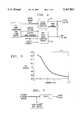
- FIG. 1illustrates a plasma etching step in fabricating an integrated circuit.
- FIG. 2illustrates a neural network process monitor for regulating a manufacturing process.
- FIG. 3illustrates a plot of a typical emission trace.
- FIG. 4illustrates a block diagram system for training a neural network.
- FIG. 5illustrates the average resulting gate thickness as a function of the number of learning trials for the neural network.
- FIG. 6illustrates the performance of the neural network as a function of data base size.
- FIG. 7illustrates a neural network controller which monitors input control variables and materials to regulate a manufacturing process.
- FIG. 8illustrates a schematic of a feedforward neural network.
- FIG. 9illustrates the adaptive procedure for adjusting the weight matrix elements.
- FIG. 10illustrates a genetic layer in a feed forward network.
- FIG. 11illustrates a neural network process monitor and database for regulating a manufacturing process.
- FIG. 12illustrates a block diagram system for training a neural network using database information.
- FIG. 1illustrates typical use of the plasma etching process as one step in fabricating a MOS transistor.
- Silicon wafer substrate 10is covered by oxide layer 12.
- Oxide layer 12is then covered with polysilicon layer 14 and tantalum silicon layer 16.
- Oxide layer 12, typically silicon dime,has a well 13 in it.
- a layer of photoresist material 18is applied to a portion of well 13, and tantalum silicon layer 16 and polysilicon layer 14 are etched away.
- etching away polysilicon layer 14it is important that all of polysilicon layer 14 be removed. However, in etching polysilicon layer 14 completely a portion 21 of oxide layer 12 will inevitably be etched. In the etching process, a critical quality attribute is remaining oxide thickness 20 in the source region 22 and drain region 24 which determines the characteristics of these regions. Remaining oxide thickness 20 is a function of the etch time, i.e. the period for which the wafer is exposed to the plasma.
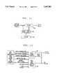
- FIG. 2presents an illustrative embodiment of the present invention in which a neural network is advantageously incorporated into process monitor 202 which regulates or governs the materials and control variables input into process 204 to produce a desired quality attribute in the output product.
- Section IIpresents an illustrative embodiment of the invention in which the plasma etch time in the fabrication of integrated circuits is controlled by a neural network process monitor which uses a portion of the trace of the optical emission to produce a desired oxide thickness on a wafer.
- An overview of neural network operation and the preferred back-propagation training techniqueare discussed in Section III.
- a trace or recordmay generally be defined as a measurement over time of a specific variable or function.
- a portion of the trace of the optical emission spectrum from the plasma glow, measured at a specified wavelength as a function of time,is used as a process signature.
- a process signaturereflects, or has embedded in it, information related to quality attributes and to the process itself as well as information about factors which make the process difficult to control.
- the optical emission tracereflects information directly related to the chemistry of the plasma and information regarding the concentration of the material etched away. Indirectly, its behavior contains information about aging of the machine, pattern density of the wafers, non-ideal fluctuations in gas flow, pressure, RF power, etc.
- process signaturesmay also be identified and used to train a neural network and to control a process.
- traces of the input control variables and materialssuch as power, temperature, pressure, etc.
- a set pointi.e. a desired or fixed value, is generally selected for each of the inputs.
- the inputswill fluctuate around these set points.
- the variationsmay reflect the progress of the process in producing an output with specified quality attributes, and thus these traces may be process signatures which can be used to train the neural network and to control the process.
- FIG. 3is a plot of a typical emission trace which in the preferred embodiment indicates the amount of chlorine gas in the plasma.
- the chlorine gas emissionwas measured at a wavelength of 837 nanometers.
- the time unitsare based on the frequency of data collection which, in this case, is approximately 1.9 sec. per unit.
- the secondis for a polysilicon etch.
- some of the underlying oxide in the exposed source and drain regionswill inevitably be etched.
- the amount etchedis dependent on the selectivity of the polysilicon etch conditions toward the oxide, and is a parameter of critical concern in the device fabrication.
- the instrumentis auto-zeroed, which normalizes the trace data.
- the auto-zeroing or normalizing stepis important because the trace has information not only about emission intensity but also about the last cleaning of the chamber. Thus, the auto-zero step adjusts the signal to allow for fogging of the optical windows as the machine ages.
- the waferis transferred to a second chamber for the polysilicon etch under a different chemistry.
- the spike at t ⁇ 115occurs at the turn on of the RF power for the polysilicon etch.
- One current method of etch end-point detectionis to observe the time at which the trace crosses a threshold, and then to etch for an additional time which is a predetermined fraction of the initial etch time.
- threshold point at about 82 time unitsThis represents the end-point of the TaSi etch and the time from 82 to 115 is the TaSi over-etch time.
- the threshold point at about 145signals the end-point of the polysilicon etch and the time from 145 to 170 is the over-etch time for the polysilicon etch.
- the neural network controllerillustratively uses as input twenty-four measurements of the polysilicon etch's emission trace. The first seven measurements typically are skipped to avoid the spike at turn-on. The next twenty-four data points typically constitute the first one-third of the total etching time. This ensures that the input data can be collected well before the etch is completed. This input is used to train the neural network to compute the optimum total etch time to obtain a target oxide thickness in the source and drain regions.
- FIG. 4is an illustrative diagram of the method of training the neural network.
- the neural network 402is a 24 ⁇ 5 ⁇ 1 architecture (i.e. 24 input nodes, 5 hidden nodes and 1 output node) and trained with the back-propagation technique (see Section III below). Results from a production database may be used for the training. Since such results will show a spread in observed oxide thicknesses, it becomes necessary to compute for each run in the database the time that would have been required to achieve the optimal result. The oxide thickness and etch time from each run can be corrected, using the known rate of oxide etching in the polysilicon etch chamber, to compute a first-order correction on the etch time. This corrected etch time is then used as the target for training the neural network. Thus, the network is trained directly with measurements of the attribute which determine product quality.
- the first order linear correction process 405computes the ideal etch time. If the oxide thickness T obs and the etch time t obs from some real world observations are known, then given the etch rate E R and the desired thickness T des we can compute an ideal etch time for this desired thickness: ##EQU1## The difference between the ideal etch time and the neural network's guessed or estimated etch time is fed back to the neural network as an error signal from which the neural network can compute new values in the weight matrices. In all of the examples in the database, the observed etch time is close to the ideal one, and the first-order corrections are small. It is important to keep in mind, however, that this kind of linear correction is only valid for making these small corrections near the end of the etch process. The earlier steps in the etch sequence, which encounter different layers and transient effects at turn-on time, are highly nonlinear and less well-behaved. These steps will be accounted for in an actual experimental database.
- the data setmay be partitioned into two sections. One section is used for training and the other section is used for testing.
- the preferred embodimentstarted with 650 examples, from which 50 were separated for testing, and 600 were used to train the network. Of these 650 examples the pattern density of the product being etched varied by as much as 50%. This pattern density information is, of course, also embedded in the trace file so it was not explicitly considered. It is assumed in such an approach that there is enough information in the trace file to accurately predict the correct etch time and that pattern density need not be explicitly included in the network's input.
- the trainingconsisted of repeated random selection of examples from the training set and back-propagating the resulting errors to update the connection matrices.
- the trainingwas stopped after every 1000 trials and the performance of the network was tested with the test set. These results are shown in FIG. 5.
- the oxide thickness before etchwas 208A. Since the network before training has very small weights, its initial output was near zero etch time, so the resulting oxides in the test data would have been unetched. After repeated training the network guesses improved, until after 50,000 training cycles the computed etch times were resulting in an average oxide thickness of 145 A, compared with a target value equal to the value for human assisted methods of 151 A. More importantly, the current, human assisted method results in a standard deviation of 15.1 A in the oxide thicknesses. The neural network showed an equivalent spread of 15.0 A.
- FIG. 7illustrates another embodiment of the invention.
- the neural networkis again trained with production data measurements of quality attributes.
- the process signatures monitored by the neural networkmay be portions of the traces of a plurality of input control variables and materials. For example, RF power, gas flow and pressure could be advantageously used to compute the total etch time.
- the neural networkmonitor some physical characteristics or manifestations of the complete manufacturing process which reflect or have embedded in them information sufficient to assure process quality as measured by attributes of the output product.
- FIG. 11illustrates a further embodiment of the invention in which neural network process monitor 202 advantageously uses input information from database 1106 as well as input from the process signature to regulate the material and control variables input to process 204 to produce an output product with the desired quality attributes.
- Database 1106may be any information storage system, but preferably any such system should be capable of dynamically accessing information in real time in response to interrogations from neural network process monitor 202. The additional information in database 1106 can result in improved network training and control of process variables.
- database 1106may contain information regarding process signatures (other than optical emission trace) and parameters (e.g. number of chips per wafer; RF power, DC bias and etch times from previous lots; and statistical data relating to observed oxide thickness in previous lots). More generally, the type of information in database 1106 will vary depending on the type and variety of input materials and control variables as well as the process signatures and process variables used for a given process.
- the information in database 1106may be used to train the neural network as show.
- the training processis similar to that as described for and shown in FIG. 4.
- FIG. 12illustrates that other process signatures as well as observations and statistics of previous and current lots may be used to train the neural network.
- this techniquedemonstrates the ability of a neural network to extract useful information from complex data.
- the physics needed to monitor the progress of a plasma etching procedure based on the optical emission trace alonewould probably be prohibitively difficult.
- the neural networksimply learns by trial and error to extract the appropriate information.
- this techniquecan be applied to many similar control problems provided the data in the process monitor has embedded within it the necessary information.
- Neural networksare loosely modeled after biological neural networks. The underlying physical models for these networks have developed from early attempts to model the behavior of their biological counterparts. These networks generally consist of layers of active elements, neurons, coupled together by variable strength connection matrices simulating the synapses found in biological networks. Layered networks of interconnected, nonlinear neurons are finding increasing use in problems such as pattern recognition, signal processing, systems identification, speech processing and robotics and machine control. Their most powerful advantage is their ability to adaptively learn to emulate the behavior of other nonlinear systems. This adaptive learning process is based on a trial and error approach in which the network is gradually modified until it exhibits the desired characteristics. For a historical review of neural network techniques, see B. Widrow & M. A. Lehr, "30 Years of Adaptive Neural Networks: Perception, Madaline, and Backpropagation," Proc. IEEE, Vol. 78, No. 9, 1415-1442 (September 1990).
- FIG. 8is a schematic of a typical feedforward neural network in which neurons 805-811 (also called nodes) are indicated by rectangles and synaptic connections 815-816 are indicated by the lines connecting each node.
- neurons 805-811also called nodes
- synaptic connections 815-816are indicated by the lines connecting each node.
- a distinguishing characteristic of these networksis the absence of feedback. Signals flow in parallel paths through them, connecting only to nodes further downstream.
- this highly parallel architectureallows them to perform at a high equivalent computational rate.
- Software networksbased on this physical model, do not realize the same benefits of parallelism, but can still exploit the ability of these networks to adaptively learn.
- the algorithms that have been developed to design neural networks that do particular computational tasksapply equally well to both hardware and software networks.
- Layers of neurons that are not directly connected to the outputare often called hidden layers. Only one hidden layer, nodes 805-809, is shown in FIG. 8. Each neuron acts as a summing node, collecting a weighted sum of all the signals in the previous layer. In addition, each has associated with it response curve 820 called its activation function.
- the hidden neuronsare usually chosen to have a sigmoidal, or step shaped, activation function.
- the hyperbolic tangent, arc tangent and Fermi functionsare examples of mathematical functions that are commonly used in software networks, all of which have the correct shape and give comparable results. Their sigmoidal shape is important.
- the nonlinearitycan be used by the adaptive network to construct nonlinear output responses.
- the hyperbolic tangent functionis illustratively used in the preferred embodiment.
- the activation function for output neurons 810-811 in the last layeris usually linear. This gives an unlimited dynamic range, allowing the network to generate arbitrarily large output signals.
- the interconnections between the layers of neuronsare variable connection strength coefficients in a weight matrix.
- the physical architecture shown in FIG. 8is described by the equation ##EQU2## This relation describes o k , the linear output of the kth neuron in the output layer, for a set of inputs, i i . Equations for networks with more hidden layers would contain an additional summation and nonlinear activation function for each additional layer.
- the matrix W1is the input-to-hidden layer matrix
- the W2 matrixis the hidden-to-output matrix.
- the training of a neural network by the back-propagation techniqueconsists of adjusting the elements of several matrices in order to minimize the error between the network output and the target response.
- This methodis a generalization of the delta rule, see Rumelhart, supra, at 321, and is based on a gradient descent optimization technique. It attempts to minimize the mean-squared error in the output of the network, as compared to a desired response.
- the rms erroris given by ##EQU3## where t k and o k are the target and the output values for the k th component of the vectors.
- the networkis time invariant, then its output will depend only on its inputs, i i and the current value of the connection weight matrices, W1 ij and W2 jk , as in Equation 1.
- the erroris determined by the values of the weighting coefficients that connect the network.
- the method used in the adaptive procedureis to change these connections by an amount proportional to the gradient of the error in weight space, i.e. for a given weight coefficient w ij , ##EQU4##
- FIG. 10shows a genetic layer within a network.
- the output of the layeris a vector of signals o j .
- Its input vector, o imay itself be an output from a preceding layer.
- Output vector o jmay, in turn, provide input to the next layer.
- Neurons 1001-1004have an activation function f j and are coupled to the input vector by a weight matrix w ij .
- the net input to each neuronis given by ##EQU5## and the output vector is given by
- ⁇is the learning rate, and is the constant of proportionality implicit in Equation 3. If the layer in question is an output layer, then ⁇ j is given by
- t jis the target, or desired, output vector and f' j denotes the differential of the neuron's activation function with respect to the input signal.
- f' jis just a constant (usually unity).
- ⁇ jis computed iteratively using ##EQU6## where ⁇ k and w jk refer to the layer immediately after the one in question (i.e. to the right of the layer in FIG. 7).
- the inputis first propagated forward through the network.
- the weight changesare first computed in the last layer, using Equations 7 and 8, and then working backwards through the network layer by layer using Equations 6 and 8.
- neural networksare, in essence, a nonparametric nonlinear learning algorithm. No assumptions are made about the populations of the variables and no assumptions are made about the functional relations of the variables. The only assumption is that there is a cause and effect relation between the inputs and the outputs which can be learned by the neural network.
- S. W. Weiss and C. A. KulokowskiComputer Systems That Learn: Classification and Prediction Methods from Statistics, Neural Nets, Machine Learning, and Expert Systems, Morgan Kaufman, San Mateo, Calif. (1991); K. Hornik, M. Stinchcombe and H. White, Universal Approximation of Unknown Mapping and its Derivatives Using Multilayer Feedforward Networks, Neural Networks, Vol. 3, 551-560 (1990).
- neural networkscould play a role in the integrated circuit fabrication process.
- information about the process signaturecan be used to train the neural network and to make predictions about the etch time adjustment as demonstrated by the description of the preferred embodiment in Section II above.
- the neural network controller as describedproduced a standard deviation of oxide thickness comparable to human assisted methods.
- the neural network controlleroffer advantages on terms of greater uniformity of product quality resulting in higher yields and lower costs in the manufacturing process.
Landscapes
- Engineering & Computer Science (AREA)
- Physics & Mathematics (AREA)
- Artificial Intelligence (AREA)
- Plasma & Fusion (AREA)
- Chemical & Material Sciences (AREA)
- Analytical Chemistry (AREA)
- Evolutionary Computation (AREA)
- Software Systems (AREA)
- General Physics & Mathematics (AREA)
- Computer Vision & Pattern Recognition (AREA)
- Medical Informatics (AREA)
- Health & Medical Sciences (AREA)
- Automation & Control Theory (AREA)
- Theoretical Computer Science (AREA)
- Data Mining & Analysis (AREA)
- Databases & Information Systems (AREA)
- Mathematical Physics (AREA)
- General Engineering & Computer Science (AREA)
- Drying Of Semiconductors (AREA)
Abstract
Description
o.sub.j =f.sub.j (net.sub.j). (5)
Δw.sub.ij =ηo.sub.i δ.sub.j. (6)
δ.sub.j =(t.sub.j -o.sub.j)f'.sub.j (net.sub.j), (7)
Claims (20)
Priority Applications (8)
| Application Number | Priority Date | Filing Date | Title |
|---|---|---|---|
| US08/150,261US5467883A (en) | 1992-12-14 | 1993-11-17 | Active neural network control of wafer attributes in a plasma etch process |
| TW082110061ATW233370B (en) | 1992-12-14 | 1993-11-29 | |
| SG1996004001ASG70554A1 (en) | 1992-12-14 | 1993-12-03 | Active neural network control of wafer attributes in a plasma etch process |
| EP93309691AEP0602855A1 (en) | 1992-12-14 | 1993-12-03 | Active neural network control of wafer attributes in a plasma etch process |
| KR1019930027406AKR100288456B1 (en) | 1992-12-14 | 1993-12-13 | Method of using neural network, method and apparatus for controlling process variable set, method and apparatus for etching time control |
| JP5342036AJPH06348679A (en) | 1992-12-14 | 1993-12-14 | Usage method of neural network |
| US08/446,122US5653894A (en) | 1992-12-14 | 1995-05-19 | Active neural network determination of endpoint in a plasma etch process |
| US08/468,167US5737496A (en) | 1993-11-17 | 1995-06-06 | Active neural network control of wafer attributes in a plasma etch process |
Applications Claiming Priority (2)
| Application Number | Priority Date | Filing Date | Title |
|---|---|---|---|
| US99030892A | 1992-12-14 | 1992-12-14 | |
| US08/150,261US5467883A (en) | 1992-12-14 | 1993-11-17 | Active neural network control of wafer attributes in a plasma etch process |
Related Parent Applications (1)
| Application Number | Title | Priority Date | Filing Date |
|---|---|---|---|
| US99030892AContinuation-In-Part | 1992-12-14 | 1992-12-14 |
Related Child Applications (2)
| Application Number | Title | Priority Date | Filing Date |
|---|---|---|---|
| US08/446,122Continuation-In-PartUS5653894A (en) | 1992-12-14 | 1995-05-19 | Active neural network determination of endpoint in a plasma etch process |
| US08/468,167DivisionUS5737496A (en) | 1993-11-17 | 1995-06-06 | Active neural network control of wafer attributes in a plasma etch process |
Publications (1)
| Publication Number | Publication Date |
|---|---|
| US5467883Atrue US5467883A (en) | 1995-11-21 |
Family
ID=46248235
Family Applications (1)
| Application Number | Title | Priority Date | Filing Date |
|---|---|---|---|
| US08/150,261Expired - LifetimeUS5467883A (en) | 1992-12-14 | 1993-11-17 | Active neural network control of wafer attributes in a plasma etch process |
Country Status (3)
| Country | Link |
|---|---|
| US (1) | US5467883A (en) |
| KR (1) | KR100288456B1 (en) |
| TW (1) | TW233370B (en) |
Cited By (68)
| Publication number | Priority date | Publication date | Assignee | Title |
|---|---|---|---|---|
| US5654903A (en)* | 1995-11-07 | 1997-08-05 | Lucent Technologies Inc. | Method and apparatus for real time monitoring of wafer attributes in a plasma etch process |
| US5658423A (en)* | 1995-11-27 | 1997-08-19 | International Business Machines Corporation | Monitoring and controlling plasma processes via optical emission using principal component analysis |
| US5681486A (en)* | 1996-02-23 | 1997-10-28 | The Boeing Company | Plasma descaling of titanium and titanium alloys |
| US5711843A (en)* | 1995-02-21 | 1998-01-27 | Orincon Technologies, Inc. | System for indirectly monitoring and controlling a process with particular application to plasma processes |
| US5740324A (en)* | 1990-10-10 | 1998-04-14 | Honeywell | Method for process system identification using neural network |
| US5780315A (en)* | 1995-09-11 | 1998-07-14 | Taiwan Semiconductor Manufacturing Company, Ltd | Dry etch endpoint method |
| US5841651A (en)* | 1992-11-09 | 1998-11-24 | The United States Of America As Represented By The United States Department Of Energy | Closed loop adaptive control of spectrum-producing step using neural networks |
| US5871658A (en)* | 1997-01-13 | 1999-02-16 | Taiwan Semiconductor Manufacturing Company, Ltd. | Optical emisson spectroscopy (OES) method for monitoring and controlling plasma etch process when forming patterned layers |
| DE19737244A1 (en)* | 1997-08-27 | 1999-03-04 | Harald Tobies | Device and method for regulating the phase position of high-frequency electrodes in plasma processes |
| US5964980A (en)* | 1998-06-23 | 1999-10-12 | Vlsi Technology, Inc. | Fitted endpoint system |
| US6077387A (en)* | 1999-02-10 | 2000-06-20 | Stmicroelectronics, Inc. | Plasma emission detection for process control via fluorescent relay |
| US6077386A (en)* | 1998-04-23 | 2000-06-20 | Sandia Corporation | Method and apparatus for monitoring plasma processing operations |
| US6090302A (en)* | 1998-04-23 | 2000-07-18 | Sandia | Method and apparatus for monitoring plasma processing operations |
| US6123983A (en)* | 1998-04-23 | 2000-09-26 | Sandia Corporation | Method and apparatus for monitoring plasma processing operations |
| US6129807A (en)* | 1997-10-06 | 2000-10-10 | Applied Materials, Inc. | Apparatus for monitoring processing of a substrate |
| US6132577A (en)* | 1998-04-23 | 2000-10-17 | Sandia Corporation | Method and apparatus for monitoring plasma processing operations |
| US6134005A (en)* | 1998-04-23 | 2000-10-17 | Sandia Corporation | Method and apparatus for monitoring plasma processing operations |
| US6153115A (en)* | 1997-10-23 | 2000-11-28 | Massachusetts Institute Of Technology | Monitor of plasma processes with multivariate statistical analysis of plasma emission spectra |
| US6157900A (en)* | 1994-10-19 | 2000-12-05 | Intellisense Corp. | Knowledge based system and method for determining material properties from fabrication and operating parameters |
| US6157447A (en)* | 1998-04-23 | 2000-12-05 | Sandia Corporation | Method and apparatus for monitoring plasma processing operations |
| US6165312A (en)* | 1998-04-23 | 2000-12-26 | Sandia Corporation | Method and apparatus for monitoring plasma processing operations |
| US6169933B1 (en) | 1998-04-23 | 2001-01-02 | Sandia Corporation | Method and apparatus for monitoring plasma processing operations |
| US6192826B1 (en)* | 1998-04-23 | 2001-02-27 | Sandia Corporation | Method and apparatus for monitoring plasma processing operations |
| US6221679B1 (en)* | 1998-04-23 | 2001-04-24 | Sandia Corporation | Method and apparatus for monitoring plasma processing operations |
| US6223755B1 (en) | 1998-04-23 | 2001-05-01 | Sandia Corporation | Method and apparatus for monitoring plasma processing operations |
| US6246473B1 (en) | 1998-04-23 | 2001-06-12 | Sandia Corporation | Method and apparatus for monitoring plasma processing operations |
| US6254717B1 (en) | 1998-04-23 | 2001-07-03 | Sandia Corporation | Method and apparatus for monitoring plasma processing operations |
| US20010007778A1 (en)* | 1999-12-29 | 2001-07-12 | Winbond Electronics Corp. | Method and system of frequency modulated end-point detection |
| US6261470B1 (en) | 1998-04-23 | 2001-07-17 | Sandia Corporation | Method and apparatus for monitoring plasma processing operations |
| US6269278B1 (en) | 1998-04-23 | 2001-07-31 | Sandia Corporation | Method and apparatus for monitoring plasma processing operations |
| US6275740B1 (en) | 1998-04-23 | 2001-08-14 | Sandia Corporation | Method and apparatus for monitoring plasma processing operations |
| US6390019B1 (en) | 1998-06-11 | 2002-05-21 | Applied Materials, Inc. | Chamber having improved process monitoring window |
| US6401082B1 (en)* | 1999-11-08 | 2002-06-04 | The United States Of America As Represented By The Secretary Of The Air Force | Autoassociative-heteroassociative neural network |
| US6419801B1 (en) | 1998-04-23 | 2002-07-16 | Sandia Corporation | Method and apparatus for monitoring plasma processing operations |
| US20030058428A1 (en)* | 2001-07-03 | 2003-03-27 | Kyoung Shik Jun | Method for controlling a processing apparatus |
| US6567717B2 (en)* | 2000-01-19 | 2003-05-20 | Advanced Micro Devices, Inc. | Feed-forward control of TCI doping for improving mass-production-wise, statistical distribution of critical performance parameters in semiconductor devices |
| US6590179B2 (en)* | 2000-09-22 | 2003-07-08 | Hitachi, Ltd. | Plasma processing apparatus and method |
| WO2003058687A1 (en)* | 2001-12-31 | 2003-07-17 | Tokyo Electron Limited | Method of detecting, identifying and correcting process performance |
| WO2003025689A3 (en)* | 2001-09-14 | 2003-10-16 | Ibex Process Technology Inc | Large scale process control by driving factor identification |
| US6649075B1 (en) | 1996-07-23 | 2003-11-18 | Applied Materials, Inc. | Method and apparatus for measuring etch uniformity of a semiconductor wafer |
| US20030236759A1 (en)* | 2002-06-21 | 2003-12-25 | Tsung-Hsuan Ho | Neural network for determining the endpoint in a process |
| US6675137B1 (en)* | 1999-09-08 | 2004-01-06 | Advanced Micro Devices, Inc. | Method of data compression using principal components analysis |
| US6673199B1 (en) | 2001-03-07 | 2004-01-06 | Applied Materials, Inc. | Shaping a plasma with a magnetic field to control etch rate uniformity |
| US20040019470A1 (en)* | 2002-07-19 | 2004-01-29 | Ibex Process Technology, Inc. | Control of complex manufacturing processes using continuous process data |
| US20040049297A1 (en)* | 2002-09-05 | 2004-03-11 | Card Jill P. | Intelligent control for process optimization and parts maintenance |
| US6718221B1 (en) | 2002-05-21 | 2004-04-06 | University Of Kentucky Research Foundation | Nonparametric control chart for the range |
| US20040076944A1 (en)* | 2002-08-22 | 2004-04-22 | Ibex Process Technology, Inc. | Supervised learning in the presence of null data |
| US20040118516A1 (en)* | 2002-12-23 | 2004-06-24 | Gunter Grasshoff | Plasma parameter control using learning data |
| US20040168108A1 (en)* | 2002-08-22 | 2004-08-26 | Chan Wai T. | Advance failure prediction |
| US20040199362A1 (en)* | 2003-03-13 | 2004-10-07 | An Cao | Intelligent modelling of process and tool health |
| US6813534B2 (en) | 1998-07-10 | 2004-11-02 | Zhifeng Sui | Endpoint detection in substrate fabrication processes |
| US20050033709A1 (en)* | 2003-05-23 | 2005-02-10 | Zhuo Meng | Adaptive learning enhancement to automated model maintenance |
| US20050087298A1 (en)* | 2001-09-06 | 2005-04-28 | Junichi Tanaka | Method of monitoring and/or controlling a semiconductor manufacturing apparatus and a system therefor |
| US20050199341A1 (en)* | 2002-10-01 | 2005-09-15 | Tokyo Electron Limited | Method and system for analyzing data from a plasma process |
| US20050220984A1 (en)* | 2004-04-02 | 2005-10-06 | Applied Materials Inc., A Delaware Corporation | Method and system for control of processing conditions in plasma processing systems |
| US6980875B1 (en) | 2003-05-21 | 2005-12-27 | University Of Kentucky Research Foundation | Nonparametric control chart for the range |
| US20060036345A1 (en)* | 2004-08-09 | 2006-02-16 | An Cao | Systems and method for lights-out manufacturing |
| US20060287753A1 (en)* | 2005-06-16 | 2006-12-21 | Jason Plumhoff | Process change detection through the use of evolutionary algorithms |
| US20080155442A1 (en)* | 2003-11-10 | 2008-06-26 | Pannese Patrick D | Methods and systems for controlling a semiconductor fabrication process |
| US20080155447A1 (en)* | 2003-11-10 | 2008-06-26 | Pannese Patrick D | Methods and systems for controlling a semiconductor fabrication process |
| US20080163094A1 (en)* | 2003-11-10 | 2008-07-03 | Pannese Patrick D | Methods and systems for controlling a semiconductor fabrication process |
| US20090259332A1 (en)* | 2008-04-09 | 2009-10-15 | Inotera Memories, Inc. | Fuzzy control method for adjusting a semiconductor machine |
| WO2013006775A1 (en)* | 2011-07-07 | 2013-01-10 | Lam Research Corporation | Methods for automatically determining capacitor values and systems thereof |
| US20130026136A1 (en)* | 2011-07-29 | 2013-01-31 | Qualcomm Mems Technologies, Inc. | Sputter-etch tool and liners |
| US10001760B1 (en)* | 2014-09-30 | 2018-06-19 | Hrl Laboratories, Llc | Adaptive control system capable of recovering from unexpected situations |
| US10691016B2 (en) | 2017-10-31 | 2020-06-23 | Samsung Electronincs Co., Ltd. | Methods of forming semiconductors using etching effect predictions and methods for determining input parameters for semiconductor formation |
| JP2023500581A (en)* | 2019-10-08 | 2023-01-10 | インターナショナル・ビジネス・マシーンズ・コーポレーション | Tool Control Using Multi-Stage LSTM for Predicting On-Wafer Measurements |
| US20230245872A1 (en)* | 2020-07-08 | 2023-08-03 | University Of Exeter | Control of Processing Equipment |
Families Citing this family (3)
| Publication number | Priority date | Publication date | Assignee | Title |
|---|---|---|---|---|
| WO2009023124A1 (en)* | 2007-08-10 | 2009-02-19 | Applied Materials, Inc. | Methods and apparatus for ex situ seasoning of electronic device manufacturing process components |
| US20150301510A1 (en)* | 2014-04-22 | 2015-10-22 | Siegmund Düll | Controlling a Target System |
| KR102527605B1 (en)* | 2017-10-31 | 2023-05-02 | 한국전자기술연구원 | Multiple Neural Network Configuration Method for Generating Multiple Analog Control Variables |
Citations (1)
| Publication number | Priority date | Publication date | Assignee | Title |
|---|---|---|---|---|
| US5286947A (en)* | 1992-09-08 | 1994-02-15 | General Electric Company | Apparatus and method for monitoring material removal from a workpiece |
- 1993
- 1993-11-17USUS08/150,261patent/US5467883A/ennot_activeExpired - Lifetime
- 1993-11-29TWTW082110061Apatent/TW233370B/zhnot_activeIP Right Cessation
- 1993-12-13KRKR1019930027406Apatent/KR100288456B1/ennot_activeExpired - Lifetime
Patent Citations (1)
| Publication number | Priority date | Publication date | Assignee | Title |
|---|---|---|---|---|
| US5286947A (en)* | 1992-09-08 | 1994-02-15 | General Electric Company | Apparatus and method for monitoring material removal from a workpiece |
Non-Patent Citations (11)
| Title |
|---|
| C. D. Himmel et al., "A Comparison of Statistically-Based and Neural Network Models of Plasma Etch Behavior," IEEE/SEMI Int. Semiconductor Manufacturing Science Symposium, 124-129 (Jun. 15-16, 1992). |
| C. D. Himmel et al., A Comparison of Statistically Based and Neural Network Models of Plasma Etch Behavior, IEEE/SEMI Int. Semiconductor Manufacturing Science Symposium, 124 129 (Jun. 15 16, 1992).* |
| E. A. Rietman et al., "Active Neutral Network Control of Wafer Attributes in a Plasma Etch Process," J. Vac. Sci. Technol. B 11(4), 1314-1316 (Jul./Aug. 1993). |
| E. A. Rietman et al., Active Neutral Network Control of Wafer Attributes in a Plasma Etch Process, J. Vac. Sci. Technol. B 11(4), 1314 1316 (Jul./Aug. 1993).* |
| European Patent Application No. 90313203.3 published in Europe on Aug. 28, 1991 by Cummings et al. Translation: yes.* |
| R. Shadmehr et al., "Principal Component Analysis of Optical Emission Spectroscopy and Mass Spectrometry: Application to Reactive Ion Etch Process Parameter Estimation Using Neural Networks," J. Electrochem. Soc., vol. 139, No. 3, 907-914 (Mar. 1992). |
| R. Shadmehr et al., Principal Component Analysis of Optical Emission Spectroscopy and Mass Spectrometry: Application to Reactive Ion Etch Process Parameter Estimation Using Neural Networks, J. Electrochem. Soc., vol. 139, No. 3, 907 914 (Mar. 1992).* |
| S S. Chen, Intelligent Control of Semiconductor Manufacturing Processes, IEEE International Conference on Fuzzy Systems, 101 108 (Mar. 8 12, 1992).* |
| S-S. Chen, "Intelligent Control of Semiconductor Manufacturing Processes," IEEE International Conference on Fuzzy Systems, 101-108 (Mar. 8-12, 1992). |
| Widrow et al, "30 Years of Adaptive Neural Networks: Perception, Madaline, and Backpropagation", Proceedings of the IEEE, vol. 78, No. 9, Sep. 1990. |
| Widrow et al, 30 Years of Adaptive Neural Networks: Perception, Madaline, and Backpropagation , Proceedings of the IEEE, vol. 78, No. 9, Sep. 1990.* |
Cited By (106)
| Publication number | Priority date | Publication date | Assignee | Title |
|---|---|---|---|---|
| US5740324A (en)* | 1990-10-10 | 1998-04-14 | Honeywell | Method for process system identification using neural network |
| US5841651A (en)* | 1992-11-09 | 1998-11-24 | The United States Of America As Represented By The United States Department Of Energy | Closed loop adaptive control of spectrum-producing step using neural networks |
| US6157900A (en)* | 1994-10-19 | 2000-12-05 | Intellisense Corp. | Knowledge based system and method for determining material properties from fabrication and operating parameters |
| US5711843A (en)* | 1995-02-21 | 1998-01-27 | Orincon Technologies, Inc. | System for indirectly monitoring and controlling a process with particular application to plasma processes |
| US5780315A (en)* | 1995-09-11 | 1998-07-14 | Taiwan Semiconductor Manufacturing Company, Ltd | Dry etch endpoint method |
| US5654903A (en)* | 1995-11-07 | 1997-08-05 | Lucent Technologies Inc. | Method and apparatus for real time monitoring of wafer attributes in a plasma etch process |
| US5658423A (en)* | 1995-11-27 | 1997-08-19 | International Business Machines Corporation | Monitoring and controlling plasma processes via optical emission using principal component analysis |
| USRE36746E (en)* | 1996-02-23 | 2000-06-27 | The Boeing Company | Plasma descaling of titanium and titanium alloys |
| US5681486A (en)* | 1996-02-23 | 1997-10-28 | The Boeing Company | Plasma descaling of titanium and titanium alloys |
| US6649075B1 (en) | 1996-07-23 | 2003-11-18 | Applied Materials, Inc. | Method and apparatus for measuring etch uniformity of a semiconductor wafer |
| US5871658A (en)* | 1997-01-13 | 1999-02-16 | Taiwan Semiconductor Manufacturing Company, Ltd. | Optical emisson spectroscopy (OES) method for monitoring and controlling plasma etch process when forming patterned layers |
| DE19737244A1 (en)* | 1997-08-27 | 1999-03-04 | Harald Tobies | Device and method for regulating the phase position of high-frequency electrodes in plasma processes |
| US20070068456A1 (en)* | 1997-10-06 | 2007-03-29 | Michael Grimbergen | Monitoring processing of a substrate in a processing chamber |
| US20080272089A1 (en)* | 1997-10-06 | 2008-11-06 | Applied Materials, Inc. | Monitoring etching of a substrate in an etch chamber |
| US7632419B1 (en) | 1997-10-06 | 2009-12-15 | Applied Materials, Inc. | Apparatus and method for monitoring processing of a substrate |
| US6129807A (en)* | 1997-10-06 | 2000-10-10 | Applied Materials, Inc. | Apparatus for monitoring processing of a substrate |
| US6153115A (en)* | 1997-10-23 | 2000-11-28 | Massachusetts Institute Of Technology | Monitor of plasma processes with multivariate statistical analysis of plasma emission spectra |
| US6269278B1 (en) | 1998-04-23 | 2001-07-31 | Sandia Corporation | Method and apparatus for monitoring plasma processing operations |
| US6246473B1 (en) | 1998-04-23 | 2001-06-12 | Sandia Corporation | Method and apparatus for monitoring plasma processing operations |
| US6132577A (en)* | 1998-04-23 | 2000-10-17 | Sandia Corporation | Method and apparatus for monitoring plasma processing operations |
| US6157447A (en)* | 1998-04-23 | 2000-12-05 | Sandia Corporation | Method and apparatus for monitoring plasma processing operations |
| US6165312A (en)* | 1998-04-23 | 2000-12-26 | Sandia Corporation | Method and apparatus for monitoring plasma processing operations |
| US6169933B1 (en) | 1998-04-23 | 2001-01-02 | Sandia Corporation | Method and apparatus for monitoring plasma processing operations |
| US6192826B1 (en)* | 1998-04-23 | 2001-02-27 | Sandia Corporation | Method and apparatus for monitoring plasma processing operations |
| US6221679B1 (en)* | 1998-04-23 | 2001-04-24 | Sandia Corporation | Method and apparatus for monitoring plasma processing operations |
| US6223755B1 (en) | 1998-04-23 | 2001-05-01 | Sandia Corporation | Method and apparatus for monitoring plasma processing operations |
| US6134005A (en)* | 1998-04-23 | 2000-10-17 | Sandia Corporation | Method and apparatus for monitoring plasma processing operations |
| US6254717B1 (en) | 1998-04-23 | 2001-07-03 | Sandia Corporation | Method and apparatus for monitoring plasma processing operations |
| US6077386A (en)* | 1998-04-23 | 2000-06-20 | Sandia Corporation | Method and apparatus for monitoring plasma processing operations |
| US6261470B1 (en) | 1998-04-23 | 2001-07-17 | Sandia Corporation | Method and apparatus for monitoring plasma processing operations |
| US6090302A (en)* | 1998-04-23 | 2000-07-18 | Sandia | Method and apparatus for monitoring plasma processing operations |
| US6275740B1 (en) | 1998-04-23 | 2001-08-14 | Sandia Corporation | Method and apparatus for monitoring plasma processing operations |
| US20030136663A1 (en)* | 1998-04-23 | 2003-07-24 | Smith Michael Lane | Method and apparatus for monitoring plasma processing operations |
| US6123983A (en)* | 1998-04-23 | 2000-09-26 | Sandia Corporation | Method and apparatus for monitoring plasma processing operations |
| US6419801B1 (en) | 1998-04-23 | 2002-07-16 | Sandia Corporation | Method and apparatus for monitoring plasma processing operations |
| US6390019B1 (en) | 1998-06-11 | 2002-05-21 | Applied Materials, Inc. | Chamber having improved process monitoring window |
| US5964980A (en)* | 1998-06-23 | 1999-10-12 | Vlsi Technology, Inc. | Fitted endpoint system |
| US6813534B2 (en) | 1998-07-10 | 2004-11-02 | Zhifeng Sui | Endpoint detection in substrate fabrication processes |
| US6077387A (en)* | 1999-02-10 | 2000-06-20 | Stmicroelectronics, Inc. | Plasma emission detection for process control via fluorescent relay |
| US6675137B1 (en)* | 1999-09-08 | 2004-01-06 | Advanced Micro Devices, Inc. | Method of data compression using principal components analysis |
| US6401082B1 (en)* | 1999-11-08 | 2002-06-04 | The United States Of America As Represented By The Secretary Of The Air Force | Autoassociative-heteroassociative neural network |
| US6732295B2 (en)* | 1999-12-29 | 2004-05-04 | Winbond Electronics Corp. | Method and system of frequency modulated end-point detection |
| US20010007778A1 (en)* | 1999-12-29 | 2001-07-12 | Winbond Electronics Corp. | Method and system of frequency modulated end-point detection |
| US6567717B2 (en)* | 2000-01-19 | 2003-05-20 | Advanced Micro Devices, Inc. | Feed-forward control of TCI doping for improving mass-production-wise, statistical distribution of critical performance parameters in semiconductor devices |
| US6747239B2 (en) | 2000-09-22 | 2004-06-08 | Hitachi, Ltd. | Plasma processing apparatus and method |
| US6590179B2 (en)* | 2000-09-22 | 2003-07-08 | Hitachi, Ltd. | Plasma processing apparatus and method |
| US6673199B1 (en) | 2001-03-07 | 2004-01-06 | Applied Materials, Inc. | Shaping a plasma with a magnetic field to control etch rate uniformity |
| US6700648B2 (en)* | 2001-07-03 | 2004-03-02 | Samsung Electronics, Co., Ltd. | Method for controlling a processing apparatus |
| DE10213285B4 (en)* | 2001-07-03 | 2007-02-01 | Samsung Electronics Co., Ltd., Suwon | Method for controlling a photolithographic device |
| US20030058428A1 (en)* | 2001-07-03 | 2003-03-27 | Kyoung Shik Jun | Method for controlling a processing apparatus |
| US20050087298A1 (en)* | 2001-09-06 | 2005-04-28 | Junichi Tanaka | Method of monitoring and/or controlling a semiconductor manufacturing apparatus and a system therefor |
| US7343217B2 (en) | 2001-09-06 | 2008-03-11 | Hitachi, Ltd. | System for monitoring and controlling a semiconductor manufacturing apparatus using prediction model equation |
| US7058470B2 (en)* | 2001-09-06 | 2006-06-06 | Hitachi, Ltd. | Method of monitoring and/or controlling a semiconductor manufacturing apparatus and a system therefor |
| US20060212156A1 (en)* | 2001-09-06 | 2006-09-21 | Junichi Tanaka | Method of monitoring and/or controlling a semiconductor manufacturing apparatus and system therefor |
| WO2003025689A3 (en)* | 2001-09-14 | 2003-10-16 | Ibex Process Technology Inc | Large scale process control by driving factor identification |
| US6904328B2 (en) | 2001-09-14 | 2005-06-07 | Ibex Process Technology, Inc. | Large scale process control by driving factor identification |
| WO2003058687A1 (en)* | 2001-12-31 | 2003-07-17 | Tokyo Electron Limited | Method of detecting, identifying and correcting process performance |
| US20050118812A1 (en)* | 2001-12-31 | 2005-06-02 | Tokyo Elecron Limited | Method of detecting, identifying and correcting process performance |
| US6718221B1 (en) | 2002-05-21 | 2004-04-06 | University Of Kentucky Research Foundation | Nonparametric control chart for the range |
| US7403930B2 (en)* | 2002-06-21 | 2008-07-22 | Macronix International Co., Ltd. | Neural network for determining the endpoint in a process |
| US20030236759A1 (en)* | 2002-06-21 | 2003-12-25 | Tsung-Hsuan Ho | Neural network for determining the endpoint in a process |
| US20070214098A1 (en)* | 2002-06-21 | 2007-09-13 | Macronix International Co.,, Ltd. | Neural network for determining the endpoint in a process |
| US20040019470A1 (en)* | 2002-07-19 | 2004-01-29 | Ibex Process Technology, Inc. | Control of complex manufacturing processes using continuous process data |
| US20040168108A1 (en)* | 2002-08-22 | 2004-08-26 | Chan Wai T. | Advance failure prediction |
| US20040076944A1 (en)* | 2002-08-22 | 2004-04-22 | Ibex Process Technology, Inc. | Supervised learning in the presence of null data |
| US6915173B2 (en) | 2002-08-22 | 2005-07-05 | Ibex Process Technology, Inc. | Advance failure prediction |
| US6970857B2 (en) | 2002-09-05 | 2005-11-29 | Ibex Process Technology, Inc. | Intelligent control for process optimization and parts maintenance |
| US20040049297A1 (en)* | 2002-09-05 | 2004-03-11 | Card Jill P. | Intelligent control for process optimization and parts maintenance |
| US20050199341A1 (en)* | 2002-10-01 | 2005-09-15 | Tokyo Electron Limited | Method and system for analyzing data from a plasma process |
| US20040118516A1 (en)* | 2002-12-23 | 2004-06-24 | Gunter Grasshoff | Plasma parameter control using learning data |
| US7020569B2 (en) | 2003-03-13 | 2006-03-28 | Ibex Process Technology, Inc. | Intelligent modelling of process and tool health |
| US20040199362A1 (en)* | 2003-03-13 | 2004-10-07 | An Cao | Intelligent modelling of process and tool health |
| US6980875B1 (en) | 2003-05-21 | 2005-12-27 | University Of Kentucky Research Foundation | Nonparametric control chart for the range |
| US7092922B2 (en)* | 2003-05-23 | 2006-08-15 | Computer Associates Think, Inc. | Adaptive learning enhancement to automated model maintenance |
| US20050033709A1 (en)* | 2003-05-23 | 2005-02-10 | Zhuo Meng | Adaptive learning enhancement to automated model maintenance |
| US8775148B2 (en) | 2003-11-10 | 2014-07-08 | Brooks Automation, Inc. | Methods and systems for controlling a semiconductor fabrication process |
| US8612198B2 (en) | 2003-11-10 | 2013-12-17 | Brooks Automation, Inc. | Methods and systems for controlling a semiconductor fabrication process |
| US20080155445A1 (en)* | 2003-11-10 | 2008-06-26 | Pannese Patrick D | Methods and systems for controlling a semiconductor fabrication process |
| US20080155443A1 (en)* | 2003-11-10 | 2008-06-26 | Pannese Patrick D | Methods and systems for controlling a semiconductor fabrication process |
| US20080163094A1 (en)* | 2003-11-10 | 2008-07-03 | Pannese Patrick D | Methods and systems for controlling a semiconductor fabrication process |
| US20080163095A1 (en)* | 2003-11-10 | 2008-07-03 | Pannese Patrick D | Methods and systems for controlling a semiconductor fabrication process |
| US20080155442A1 (en)* | 2003-11-10 | 2008-06-26 | Pannese Patrick D | Methods and systems for controlling a semiconductor fabrication process |
| US8639365B2 (en)* | 2003-11-10 | 2014-01-28 | Brooks Automation, Inc. | Methods and systems for controlling a semiconductor fabrication process |
| US20080155447A1 (en)* | 2003-11-10 | 2008-06-26 | Pannese Patrick D | Methods and systems for controlling a semiconductor fabrication process |
| US8473270B2 (en) | 2003-11-10 | 2013-06-25 | Brooks Automation, Inc. | Methods and systems for controlling a semiconductor fabrication process |
| US8639489B2 (en) | 2003-11-10 | 2014-01-28 | Brooks Automation, Inc. | Methods and systems for controlling a semiconductor fabrication process |
| US10444749B2 (en) | 2003-11-10 | 2019-10-15 | Brooks Automation, Inc. | Methods and systems for controlling a semiconductor fabrication process |
| US8972029B2 (en) | 2003-11-10 | 2015-03-03 | Brooks Automation, Inc. | Methods and systems for controlling a semiconductor fabrication process |
| US20050220984A1 (en)* | 2004-04-02 | 2005-10-06 | Applied Materials Inc., A Delaware Corporation | Method and system for control of processing conditions in plasma processing systems |
| US20060036345A1 (en)* | 2004-08-09 | 2006-02-16 | An Cao | Systems and method for lights-out manufacturing |
| US7625824B2 (en) | 2005-06-16 | 2009-12-01 | Oerlikon Usa, Inc. | Process change detection through the use of evolutionary algorithms |
| US20060287753A1 (en)* | 2005-06-16 | 2006-12-21 | Jason Plumhoff | Process change detection through the use of evolutionary algorithms |
| US20090259332A1 (en)* | 2008-04-09 | 2009-10-15 | Inotera Memories, Inc. | Fuzzy control method for adjusting a semiconductor machine |
| US8010212B2 (en)* | 2008-04-09 | 2011-08-30 | Inotera Memories, Inc. | Fuzzy control method for adjusting a semiconductor machine |
| US10438775B2 (en) | 2011-07-07 | 2019-10-08 | Lam Research Corporation | Methods for automatically determining capacitor values and systems thereof |
| US8828259B2 (en)* | 2011-07-07 | 2014-09-09 | Lam Research Corporation | Methods for automatically determining capacitor values and systems thereof |
| WO2013006775A1 (en)* | 2011-07-07 | 2013-01-10 | Lam Research Corporation | Methods for automatically determining capacitor values and systems thereof |
| TWI584369B (en)* | 2011-07-07 | 2017-05-21 | 蘭姆研究公司 | Methods for automatically determining capacitor values and systems thereof |
| US20130008871A1 (en)* | 2011-07-07 | 2013-01-10 | Sato Arthur H | Methods for automatically determining capacitor values and systems thereof |
| US20130026136A1 (en)* | 2011-07-29 | 2013-01-31 | Qualcomm Mems Technologies, Inc. | Sputter-etch tool and liners |
| US10001760B1 (en)* | 2014-09-30 | 2018-06-19 | Hrl Laboratories, Llc | Adaptive control system capable of recovering from unexpected situations |
| US10691016B2 (en) | 2017-10-31 | 2020-06-23 | Samsung Electronincs Co., Ltd. | Methods of forming semiconductors using etching effect predictions and methods for determining input parameters for semiconductor formation |
| DE102018117836B4 (en) | 2017-10-31 | 2024-01-11 | Samsung Electronics Co., Ltd. | Methods for producing semiconductors and use of etching effect predictions |
| JP2023500581A (en)* | 2019-10-08 | 2023-01-10 | インターナショナル・ビジネス・マシーンズ・コーポレーション | Tool Control Using Multi-Stage LSTM for Predicting On-Wafer Measurements |
| US12197133B2 (en) | 2019-10-08 | 2025-01-14 | International Business Machines Corporation | Tool control using multistage LSTM for predicting on-wafer measurements |
| US20230245872A1 (en)* | 2020-07-08 | 2023-08-03 | University Of Exeter | Control of Processing Equipment |
Also Published As
| Publication number | Publication date |
|---|---|
| KR940015894A (en) | 1994-07-22 |
| KR100288456B1 (en) | 2001-05-02 |
| TW233370B (en) | 1994-11-01 |
Similar Documents
| Publication | Publication Date | Title |
|---|---|---|
| US5467883A (en) | Active neural network control of wafer attributes in a plasma etch process | |
| US5737496A (en) | Active neural network control of wafer attributes in a plasma etch process | |
| US5711843A (en) | System for indirectly monitoring and controlling a process with particular application to plasma processes | |
| US5653894A (en) | Active neural network determination of endpoint in a plasma etch process | |
| Himmel et al. | Advantages of plasma etch modeling using neural networks over statistical techniques | |
| Ingolfsson et al. | Stability and sensitivity of an EWMA controller | |
| US6970857B2 (en) | Intelligent control for process optimization and parts maintenance | |
| US5841651A (en) | Closed loop adaptive control of spectrum-producing step using neural networks | |
| Wang et al. | Artificial neural network model-based run-to-run process controller | |
| EP0602855A1 (en) | Active neural network control of wafer attributes in a plasma etch process | |
| Stokes et al. | Real-time control of reactive ion etching using neural networks | |
| Mevawalla et al. | Neural network modeling for advanced process control using production data | |
| Kozma et al. | On the accuracy of mapping by neural networks trained by backpropagation with forgetting | |
| Rietman et al. | Active neutral network control of wafer attributes in a plasma etch process | |
| Rietman et al. | A production demonstration of wafer-to-wafer plasma gate etch control by adaptive real-time computation of the over-etch time from in situ process signals | |
| Vijayakumar et al. | Local dimensionality reduction for locally weighted learning | |
| Spanos et al. | Using qualitative observations for process tuning and control [IC manufacture] | |
| Rietman et al. | Neural network control of a plasma gate etch: Early steps in wafer-to-wafer process control | |
| Himmel et al. | Real-time predictive control of semiconductor manufacturing processes using neural networks | |
| Currie et al. | Self-improving process control for molecular beam epitaxy | |
| Ahmadi et al. | Improved Machine Learning based Approach for Autotuning PID Controller using Genetic Algorithms and Parallel Processing: IMPROVED MACHINE LEARNING APPROACH FOR AUTOTUNING PID | |
| Kim et al. | Plasma diagnosis by recognizing in situ data using a modular backpropagation network | |
| Rietman et al. | Pre-production results demonstrating multiple-system models for yield analysis | |
| Rietman et al. | Modeling and control of a semiconductor manufacturing process with an automata network: An example in plasma etch processing | |
| JP2647216B2 (en) | Dead time compensation controller |
Legal Events
| Date | Code | Title | Description |
|---|---|---|---|
| AS | Assignment | Owner name:AMERICAN TELEPHONE AND TELEGRAPH COMPANY, NEW YORK Free format text:ASSIGNMENT OF ASSIGNORS INTEREST;ASSIGNORS:FRYE, ROBERT CHARLES;HARRY, THOMAS RICHARD;LORY, EARL RYAN;AND OTHERS;REEL/FRAME:006818/0256;SIGNING DATES FROM 19931119 TO 19931122 | |
| AS | Assignment | Owner name:AT&T IPM CORP., FLORIDA Free format text:ASSIGNMENT OF ASSIGNORS INTEREST;ASSIGNOR:AT&T CORP.;REEL/FRAME:007528/0038 Effective date:19950523 Owner name:AT&T CORP., NEW YORK Free format text:ASSIGNMENT OF ASSIGNORS INTEREST;ASSIGNOR:AMERICAN TELELPHONE AND TELEGRAPH COMPANY;REEL/FRAME:007527/0274 Effective date:19940420 | |
| STCF | Information on status: patent grant | Free format text:PATENTED CASE | |
| FEPP | Fee payment procedure | Free format text:PAYOR NUMBER ASSIGNED (ORIGINAL EVENT CODE: ASPN); ENTITY STATUS OF PATENT OWNER: LARGE ENTITY | |
| FPAY | Fee payment | Year of fee payment:4 | |
| FEPP | Fee payment procedure | Free format text:PAYOR NUMBER ASSIGNED (ORIGINAL EVENT CODE: ASPN); ENTITY STATUS OF PATENT OWNER: LARGE ENTITY Free format text:PAYER NUMBER DE-ASSIGNED (ORIGINAL EVENT CODE: RMPN); ENTITY STATUS OF PATENT OWNER: LARGE ENTITY | |
| FPAY | Fee payment | Year of fee payment:8 | |
| FPAY | Fee payment | Year of fee payment:12 | |
| AS | Assignment | Owner name:BELL SEMICONDUCTOR, LLC, ILLINOIS Free format text:ASSIGNMENT OF ASSIGNORS INTEREST;ASSIGNORS:AVAGO TECHNOLOGIES GENERAL IP (SINGAPORE) PTE. LTD.;BROADCOM CORPORATION;REEL/FRAME:044886/0001 Effective date:20171208 | |
| AS | Assignment | Owner name:CORTLAND CAPITAL MARKET SERVICES LLC, AS COLLATERA Free format text:SECURITY INTEREST;ASSIGNORS:HILCO PATENT ACQUISITION 56, LLC;BELL SEMICONDUCTOR, LLC;BELL NORTHERN RESEARCH, LLC;REEL/FRAME:045216/0020 Effective date:20180124 | |
| AS | Assignment | Owner name:BELL NORTHERN RESEARCH, LLC, ILLINOIS Free format text:SECURITY INTEREST;ASSIGNOR:CORTLAND CAPITAL MARKET SERVICES LLC;REEL/FRAME:060885/0001 Effective date:20220401 Owner name:BELL SEMICONDUCTOR, LLC, ILLINOIS Free format text:SECURITY INTEREST;ASSIGNOR:CORTLAND CAPITAL MARKET SERVICES LLC;REEL/FRAME:060885/0001 Effective date:20220401 Owner name:HILCO PATENT ACQUISITION 56, LLC, ILLINOIS Free format text:SECURITY INTEREST;ASSIGNOR:CORTLAND CAPITAL MARKET SERVICES LLC;REEL/FRAME:060885/0001 Effective date:20220401 |