US5467455A - Data processing system and method for performing dynamic bus termination - Google Patents
Data processing system and method for performing dynamic bus terminationDownload PDFInfo
- Publication number
- US5467455A US5467455AUS08/145,117US14511793AUS5467455AUS 5467455 AUS5467455 AUS 5467455AUS 14511793 AUS14511793 AUS 14511793AUS 5467455 AUS5467455 AUS 5467455A
- Authority
- US
- United States
- Prior art keywords
- bus
- data
- termination
- circuit
- external
- Prior art date
- Legal status (The legal status is an assumption and is not a legal conclusion. Google has not performed a legal analysis and makes no representation as to the accuracy of the status listed.)
- Expired - Lifetime
Links
Images


Classifications
- H—ELECTRICITY
- H03—ELECTRONIC CIRCUITRY
- H03H—IMPEDANCE NETWORKS, e.g. RESONANT CIRCUITS; RESONATORS
- H03H7/00—Multiple-port networks comprising only passive electrical elements as network components
- H03H7/38—Impedance-matching networks
- H03H7/40—Automatic matching of load impedance to source impedance
Definitions
- the present inventionrelates generally to data processors, and more particularly, to dynamic termination of conductive bus lines to avoid signal reflection.
- the termination problemis enhanced because either end of the bus may either be receiving or transmitting at any time. Therefore, in the prior art, permanent resistor termination is placed at both ends of the bus and are connected regardless of whether or not they are needed. This results in an increased load to the bus and increased power consumption when the bus is placed into a low power mode of operation.
- the present inventioncomprises a method for determining whether to enable termination circuitry within a data processor.
- a bus transferbegins through a bus coupled between the data processor and a device external to the data processor.
- a determinationis made as to whether the data processor is receiving data or sending data external to the processor.
- the termination circuitryis enabled if the data processor is receiving data from the bus in order to reduce signal reflection on the bus.
- the termination circuitryis disabled if the data processor is sending data through the bus.
- the inventioncomprises a data processing system having a communication device having at least one external pin connected external to the communication device.
- the at least one external pinis coupled to receive data from external to the communication device and transmit data external to the communication device.
- the communication devicehas circuitry for terminating.
- the circuitry for terminatinghas a first input/output terminal coupled to the at least one external pin via at least one data line.
- the circuitry for terminatinghas a second input/output terminal for providing or receiving data from internal to the communication device.
- the circuitry for terminatinghas an input for receiving an enable signal and has one or more termination component(s).
- the enable signalcouples the termination component to the at least one termination pin when the enable signal is asserted, and decouples the termination component from the at least one termination pin when the enable signal is deasserted.
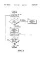
- FIG. 1illustrates, in a block diagram, a data processing system in accordance with the present invention
- FIG. 2illustrates, in a block diagram, another data processing system in accordance with the present invention
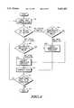
- FIG. 3illustrates, in a flowchart, a method for dynamically enabling a termination circuit of an integrated circuit in accordance with the present invention
- FIG. 4illustrates, in a flowchart, another method for dynamically enabling a termination circuit of an integrated circuit in accordance with the present invention
- FIG. 5illustrates, in a block diagram, a data processing system having a plurality of independently-enabled bus termination circuits for each external input/output integrated circuit pin in the data processing system being in accordance with the present invention
- FIG. 6illustrates, in a block diagram, an interconnection of the plurality of independently-enabled bus termination circuits of FIG. 5 in accordance with the present invention
- FIG. 7illustrates, in a block diagram, another interconnection of the plurality of independently-enabled bus termination circuits of FIG. 5 in accordance with the present invention.
- FIG. 8illustrates, in a block diagram, yet another interconnection of the plurality of independently-enabled bus termination circuits of FIG. 5 in accordance with the present invention.
- the apparatus and method illustrated hereinis designed to dynamically enable the proper termination inside a receiver at the end of the bi-directional bus.
- the proper terminationis dynamically connected to the bus only when data is being received in order to reduce signal reflection on the bus (i.e. transmission line effects) and allow for a more rapid operational speed.
- This dynamic bus terminationrequires a control signal which indicates to the receiving device the current drive direction of the bus (i.e., is data being read from the device or is data being written to the device).
- this control signalindicates the bus has a voltage and/or current which is being driven into the receiving device, the receiving device turns on its termination devices to dampen the incoming signal so no reflections are sent back down the bus (transmission line).
- the control signalindicates the bus is not being driven into the receiving device the receiving device's terminators are turned off to reduce the load on the bus and power dissipation of the bus.
- An example of devices which would use this dynamic termination methodwould be two very high speed processors which communicate through a bi-directional bus such as a data bus.
- the control signal that switches on the receiving processor's termination networkwould be the read/write (R/W*) line. It is advantageous to use a control line which will indicate the directionality of the bus in advance of the time when the data is actually transferred to allow receiving devices time to enable their respective termination networks.
- R/W*read/write
- R/W*is driven by a processor or primary bus master when the processor is the bus owner (i.e., when the processor has mastership or ownership of the bus).
- the R/W* signalindicates the direction (i.e., data going into the primary master [a read] or data going out of the primary master [a write]) of subsequent data transfer(s). It is asserted high during read bus cycles and asserted low during write bus cycles.
- the R/W* signalis tristated.
- the ⁇ * ⁇ character in a signal nameimplies that the signal is active low in some manner.
- the external resistor 11is used to stabilize the R/W* line when the R/W* line is tristated by devices 10 and 12.
- the preferred method and apparatus illustrated and taught hereinsolves the problem of properly terminating a bi-directional transmission line.
- Known techniquesinvolved terminating a bus at each end of the bus, at mid-points on the bus, or involve structuring the bus in a star-like layout with the termination network at the center of the star.
- performanceis improved.
- the apparatus and method illustrated hereinprovides the ability to dynamically terminate a bi-directional bus depending on the current bus drive direction. Since this method allows the termination network to appear where needed at the end point of the net, the transmission line can be properly terminated as if it was a uni-directional bus. This method of termination also reduces power used in the termination networks of a system since only those termination networks which are at the endpoint of the bus need be enabled.
- the transmission lineshould be properly terminated at the terminal point of the net, which is usually the input of another device, to prevent signal reflection problems.
- another device on the bi-directional busdrives the signal the proper place for the termination could be at the other end or a different point of the net, usually another input device.
- a different termination method/circuit or component valuee.g., different resistances
- FIG. 1illustrates a data processing system.
- the data processing systemhas a device 10 and a device 12 (referred to also as communication devices since they communicate to one another).
- device 10 and device 12are each integrated circuits.
- either device 10 or device 12may be a memory device (such as a SRAM, a DRAM, a EEPROM device, an EPROM device, a flash device, and the like), an interface device, any peripheral device, a DMA device, a communication device, a timer, analog circuitry, a microprocessor, a pipelined execution device, an application specific integrated circuit (ASIC) device, a programmable logic array (PLA), hard-wired logic, an execution unit at least partially software driven by microcode and/or nanocode, a plurality of execution devices, a digital signal processor (DSP), a computer, a data processor, a central processing unit (CPU), and integrated circuit, and/or the like.
- a memory devicesuch as a SRAM, a DRAM, a EEPROM device, an EPROM device, a flash device, and the like
- an interface deviceany peripheral device, a DMA device, a communication device, a timer, analog circuitry, a microprocessor, a pipelined
- the device 10has a dynamic bus termination circuit 14 connected via at least one conductor or a bi-directional bus 13 to one or more external integrated circuit data pins.
- An internal data busconnects the circuit 14 to a bi-direction circuit having a first tristate buffer 22 and a second tristate buffer 24.
- Buffers 22 and 24are turned on, usually in a mutually exclusive manner to enable bi-directional communication (time-multiplexed two-way communication).
- the buffers 22 and 24are connected to a data unit 18 which may be a memory array or a data processor CPU.
- the internal data busmay be split into two buses, one bus for reading and one bus for writing wherein no time multiplexing is needed until the external pins are reached.
- the termination circuitcontains one or more circuit components which when coupled to the data line reduce reflection or change line impedance on the bi-directional external bus 17 when data is being received by the device 10.
- the circuit componentsmay include one or more of a capacitor, a PN junction, a diode, a resistor, a resistive device, an inductor, an N channel transistor, a P channel transistor, a junction field effect transistor (JFET), a metal oxide semiconductor transistor (MOSFET), a bipolar device, a Bi-CMOS device, a current source, a voltage source, any other like termination component, or a circuit comprising one or more of the circuit elements listed above.
- the circuit component within circuit 14is coupled to the pins in response to the state of an enable control signal of FIG. 1.
- the enable signalin general, is in one logic state if a data is incoming to the device 10 and is deasserted when data is being sent out from the device 10.
- the enable signalis a function of the read/write R/W* and a mater/salve* control signal which indicates whether device 10 is a master of the bus 17 or a slave device not having ownership/mastership of bus 17.
- the logicinvolves a tristate buffer 34 and a exclusive nor (XNOR) gate 30.
- the device 12has a dynamic bus termination circuit 16, a bus 15, a internal bi-directional data bus with tristate buffers 26 and 28, a data unit 20, an XNOR gate 32, a tristate buffer 36, a master/slave* signal, and a R/W* signal all of which are analogous to corresponding elements in device 10. It is important to note that although device 10 is analogous to device 12 in FIG. 1 that the device 12 could be very different from device 12 in another form. For example, device 12 could be a memory device wherein device 10 is a microprocessor. Device 12 may not have enable logic similar to device 10 (i.e., may not have the XNOR 32 and tristate buffer 36, but other logic and other control signal inputs).
- the operation of the dynamic terminationmay be further described as follows. Assume device 10 is a bus master and device 12 is a slave device for purposes of a data transfer on bus 17. Furthermore, assume device 10 desires to make a write transfer of data to device 12. Device 10 has an internal indication that it is master of the bus 17 while device 12 has internal indication it is currently a slave on the bus 17. Device 10 will assert and drive the Read/Write* (R/W*) line via an enabled tristate buffer 34 to indicate it desires a write transfer of data to device 12. In this case, Device 10 has inputs to the exclusive-NOR (XNOR) gate 30 which are at a logical 1 and 0 causing the termination network to be disabled.
- XNORexclusive-NOR
- the termination circuitry of device 10is disabled because data is outgoing not incoming, and therefore no termination in device 10 is needed to avoid transmission line effects and/or signal reflection.
- device 12has inputs to the exclusive-NOR (XNOR) gate 32 are both at a logic 0 level causing the termination network in device 12 to be enabled.
- the termination in device 12is enabled because device 12 is receiving data on bus 17.
- the data bus transmission line 17is dynamically and properly terminated with the characteristic impedance of the line preventing signal reflection problems.
- device 10will assert and drive the R/W* line to indicate it desires a read transfer of data from device 12.
- device 10has inputs to the exclusive-NOR gate which are both at a logical 1 causing it's termination network to be enabled.
- Device 12has inputs to the exclusive-NOR gate which are at a logical 0 and 1 causing the termination network in Device 2 to be disabled.
- either device 10 or device 12has a termination network which will be dynamically enabled providing transmission line termination at the end or sink of the bus 17 lines.
- this mechanismallows the termination network to be disabled or not present when the device is not receiving data to reduce power dissipation and reduce the loading of bus lines.
- This method of terminationreduces power used in the termination networks of a system since only those termination networks which are at the endpoint of the bus need be enabled at any given time. When a bus is not being used at all, neither of the circuits 14 or 16 are enabled which further decreases power consumption.
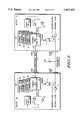
- FIG. 2illustrates a data processing system similar to FIG. 1 but further illustrates the circuits 14 and 16 of FIG. 1.
- the device 100is analogous to the device 10, and the device 200 is analogous to the device 12.
- Integrated circuit pinsare not illustrated in FIG. 2 although they are present in a preferred form.
- the tristate buffers 110, 112, 210, and 212are respectively analogous to the tristate buffers 22, 24, 26, and 28 of FIG. 1.
- the tristate buffers, 110, 112, 210, 212are enabled/disabled via a control signal R/W* (internal) and controls the direction of data flow on the bus 17.
- Resistor 111is analogous to resistor 11 of FIG. 1.
- the XNOR gates 114 and 214are analogous to the XNOR gates 30 and 32, respectively, of FIG. 1.
- the tristate buffers 116 and 216are respectively analogous to tristate buffers 34 and 36 of FIG. 1.
- circuit 14contains a bipolar transistor 102 and a bipolar transistor 108.
- Transistor 102has a collector coupled to Vdd (usually 5.0 volts or less), an emitter, and a base connected to the enable signal.
- a circuit component 104used to dynamically reduce signal reflection, has a first terminal connected to the emitter of transistor 102 and a second terminal connected/coupled to the bus 17 (output buffers, input buffers, and input/output (I/O) buffers, as needed, are not specifically illustrated in FIGS. 1-2).
- the transistor 108has an emitter connected to a ground potential, a collector, and a base connected to the enable signal.
- a component 106similar to component 104, has a first terminal connected/coupled to the bus 17 and a second terminal connected to the collector of transistor 108.
- the components 104 and 106may each be, for example a single resistor. In other forms, the components 104 and 106 may be entire circuits comprising logic gates, capacitors, PN junctions, diodes, other resistors, any resistive devices, inductors, N channel transistors, P channel transistors, JFET, bipolar transistor devices, BiCMOS devices, and the like.
- the components 104, 106are dynamically activated to the bus 17 only when data is being received by the device 100 via the bus 17.
- the components 104 and 106are selectively connected via the enable signal connected to the transistors 102 and 108. It should be noted again that other termination methods besides the thevenin-equivalent method taught herein with resistors etc. are possible.
- the point of interestis the concept of making the termination dynamic at end points of a bi-directional bus, whereas different termination may be used for each device in the data processing system.
- transistors 202 and 208 and the devices 204 and 206are analogous to elements discussed above in for device 100.
- FIG. 3illustrates a method used to dynamically terminate an integrated circuit.
- bus communicationis enabled or initiated.
- a device coupled to a bussuch as device 10 of FIG. 1, determines whether data is incoming from the bus to the device or outgoing from the device to the bus. If the data is incoming a step 304 is used to enable the termination logic in FIGS. 1-2. If the data is outgoing, no termination is needed and the termination circuitry is disabled. Once the termination circuitry is either disabled or enabled, the data is transferred with reduced signal reflection along the bus. If there is more data to transfer, the method of FIG. 3 is performed again via a step 308. In a step 309 the termination components/circuits are disabled if not needed.
- the above methodwill work for any type of bus transfer including burst bus transfers wherein multiple data values are sent in a single bus cycle.
- FIG. 4illustrates an alternative method of for performing dynamic termination.
- FIG. 4is similar to FIG. 3.
- a step 400is analogous to step 300 in FIG. 3.
- a step 402is used to determine if the device is a master device (i.e., has ownership of the bus being used to communicate information).
- Steps 404 and 406are used to determine if a read or a write operation is occurring.
- the termination circuitryis either enabled or disabled in steps 408 or 410.
- Datais transferred in a step 411 with reduced signal reflection on the bus and if more data is to be transferred, the process of FIG. 4 is repeated as illustrated in step 412.
- the transfer termination circuits/componentsare disabled if not needed.
- the state diagram of master/slave* and R/W* used to determine whether or not the termination circuitry is enabledis as follows:
- FIG. 5illustrates a system similar to FIG. 1. All the elements of FIG. 1 which are analogous to elements in FIG. 5 are identically labeled.
- FIG. 5illustrates termination circuits 500 and 501.
- the termination circuit 500contains, in FIG. 5, four dynamic bus termination circuits 14, 50, 52, and 54. It should be noted that any number of bus termination circuits may be included within circuit 500.
- N dynamic bus termination circuitsmay be serially connected and/or parallel-connected together in the circuit 500 wherein N is a finite integer greater than zero (i.e., 1, 2, 3, 4, 5, 6, . . . dynamic bus termination circuits may be used).
- Each of the bus termination circuits in circuit 500have different enable signals, therefore four enable signals are illustrated in FIG. 5.
- one or more of the enable signalsmay be enabled to connected one or more termination components/circuits to the bus to reduce signal reflection or alter line impedance.
- the enablesmay be derived internally to the device 10, may be received from external to the device 10 (i.e., from a slave device or alternate master), or may be a combination of signals internal and external to the device 10.
- Circuit 501is similar to circuit 500 and is therefore not further discussed.
- circuit 14may be enabled when the device 10 operates at 33.3 Mhz and circuit 50 enabled when the device 10 operates at 50 MHz, etc.
- the circuit 52may be enabled when the device is communicating to a slow SRAM device, whereas termination circuit 54 is enabled when communicating to a fast DRAM device, etc.
- two or more of the circuits 14, 50, 52, and 54may be simultaneously enabled to couple a plurality of termination components or circuits in either parallel or series or a combination of parallel and series.
- bus 13the bi-directional bus, and the data bus may be either one bit or more than one bit. If they are more than one bit, then circuit 500 is repeated for each bit of the bus, as in FIG. 1.
- FIG. 6illustrates the circuit 500 including the four termination circuits 14, 50, 52, and 54.
- the bus 13, the data bus and four enable lines of FIG. 5are illustrated.
- the 4 enable circuitsare split internal to circuit 500 into separately-labeled enable signals 1 through 4.
- Each termination circuitmust have a device which functions as an on/off switch (i.e. a bipolar transistor, an MOS transistor, a JFET, an SCR, a triac, a relay, etc.) and a device which functions to change the impedance of the bus or to reduce signal reflection.
- the function of switching and reducing reflectionmay be performed by a single device, such as a single transistor in the circuit/components of FIG. 6.
- Termination circuit 14has a termination circuit/component 502 coupled between the bi-directional bus and Vdd, and a termination circuit/component 510 coupled between the bi-direcitonal bus and ground.
- Termination circuit 50has a termination circuit/component 504 coupled between the bi-directional bus and Vdd, and a termination circuit/component 512 coupled between the bi-direcitonal bus and ground.
- Termination circuit 52has a termination circuit/component 506 coupled between the bi-directional bus and Vdd, and a termination circuit/component 514 coupled between the bi-direcitonal bus and ground.
- Termination circuit 54has a termination circuit/component 508 coupled between the bi-directional bus and Vdd, and a termination circuit/component 516 coupled between the bi-direcitonal bus and ground.
- circuit/component 502is in parallel with circuit/component 504 and circuit/component 510 is in parallel with circuit/component 512 to form a different termination device.
- circuit/component 502is a 100 ohm resistor and a switch
- circuit/component 504is a 50 ohm resistor and a switch
- circuit/component 506is a 10 ohm resistor and a switch
- circuit/componentis a 3 ohm resistor and a switch for sake of example. If the switches are coupled to the enable signals, then the four enables can cycle through 16 (2 4 ) different states.
- one of either 100, 50, 10, 3, 33.33, 8.33, 2.91, 7.69, 2.75, 2.16, 9.09, 2.30, 2.83, 2.20, 2.26, or ⁇ ohmscan be selectively chosen as the impedance of the bus from the bi-directional bus to the Vdd line in the circuit of FIG. 6.
- eight enable signalsmay be used in FIG. 6 wherein one enable signal is coupled to each termination circuit/component of FIG. 6. With eight enables 2 8 distinct termination values are possible.
- FIG. 7illustrates an alternative interconnection of circuits/components 520, 522, 524, 526.
- the circuits/components of FIG. 7are similar to the circuits/components of FIG. 6 wherein at least one device functioning as an on/off switch and a signal reflection reducer must be present, or multiple devices wherein the multiple device either together or in isolation perform the switching function and the reflection reducing function.
- FIG. 7illustrates that serial connections as well as parallel connections may be made via the interconnection of circuit 500. Four enable signals are illustrated. The various states of enable signals in FIG. 7 result in up to 9 distinct termination values.
- circuit/component 520is a 5 ohm resistor and a serial switch
- circuit/component 522is a 10 ohm resistor and a serial switch
- circuit/component 524is a 20 ohm resistor and a serial switch
- circuit/component 526is a 50 ohm resistor and a serial switch.
- the following termination impedancesmay result: 60, 55, 30, 25, 53.333, 23.333, 24.286, 19.286, and ⁇ ohms depending on the states of the enable signals.
- FIG. 7also illustrates that the termination circuits in FIGS. 1-7 do not always have to be coupled to both ground and Vdd. Instead a termination circuit/component may connect/couple only to either Vdd or ground.
- FIG. 8illustrates a circuit 500 which may be used to selectively couple destination series termination in series with a bus 13.
- FIG. 8illustrates four termination circuits/components 600, 601, 602, and 603 which are respectively enabled via enables 1-4. It should be noted that any number of termination circuits and components (not just four) may be connected as illustrated in FIG. 8.
- the enables 1-4may be independently asserted or asserted in groups to provide up to 16 different termination combinations for the four termination circuits/components in FIG. 8.
- One of the termination circuit/componentsmay be a direct electrical short circuit.
- more than two devices connected to the busmay be coupled to a bus in FIGS. 1-2.
- Either address buses, data buses, serial communication lines, or control signalsmay be terminated in the manner taught herein. Any termination circuit or component which reduces signal reflection may be used.
- An RC networkmay also be useful as a termination component/circuit. It is also advantageous to enable the termination component only during a brief time when data is actually transitioning on a bus.
- the data busmay have 32 bits wherein a new transfer changes the bus (for example, from an FFFFFFFF hex value to an FFFFFFF7 hex value) wherein only one bit in the 32-bit value is changing significantly.
- a new transferchanges the bus (for example, from an FFFFFFFF hex value to an FFFFFFF7 hex value) wherein only one bit in the 32-bit value is changing significantly.
- only one termination circuit in the 32 termination circuitsneed be enabled to reduce reflection.
- the proper termination value for a buscould be a series-connected resistance (series connected meaning that it is connected in-line with the bus in-between the receiving pin and an input buffer).
- the configuration of the circuits of FIG. 5may be set upon reset, externally-configurable, or may be user configurable. Other enable control signals are possible besides the enables illustrated herein.
Landscapes
- Memory System (AREA)
- Dram (AREA)
- Logic Circuits (AREA)
Abstract
Description
______________________________________ R/W* master/slave* termination enabled? ______________________________________ 0 0 yes 0 1 no 1 0 no 1 1 yes ______________________________________
Claims (29)
Priority Applications (2)
| Application Number | Priority Date | Filing Date | Title |
|---|---|---|---|
| US08/145,117US5467455A (en) | 1993-11-03 | 1993-11-03 | Data processing system and method for performing dynamic bus termination |
| JP28720694AJP4230545B2 (en) | 1993-11-03 | 1994-10-28 | Data processing system and operation method |
Applications Claiming Priority (1)
| Application Number | Priority Date | Filing Date | Title |
|---|---|---|---|
| US08/145,117US5467455A (en) | 1993-11-03 | 1993-11-03 | Data processing system and method for performing dynamic bus termination |
Publications (1)
| Publication Number | Publication Date |
|---|---|
| US5467455Atrue US5467455A (en) | 1995-11-14 |
Family
ID=22511674
Family Applications (1)
| Application Number | Title | Priority Date | Filing Date |
|---|---|---|---|
| US08/145,117Expired - LifetimeUS5467455A (en) | 1993-11-03 | 1993-11-03 | Data processing system and method for performing dynamic bus termination |
Country Status (2)
| Country | Link |
|---|---|
| US (1) | US5467455A (en) |
| JP (1) | JP4230545B2 (en) |
Cited By (108)
| Publication number | Priority date | Publication date | Assignee | Title |
|---|---|---|---|---|
| US5596757A (en)* | 1995-02-16 | 1997-01-21 | Simple Technology, Inc. | System and method for selectively providing termination power to a SCSI bus terminator from a host device |
| US5919252A (en)* | 1991-07-29 | 1999-07-06 | Micron Electronics, Inc. | Process and apparatus for adaptive bus termination |
| US6008665A (en)* | 1997-05-07 | 1999-12-28 | California Micro Devices Corporation | Termination circuits and methods therefor |
| EP0972343A4 (en)* | 1996-07-19 | 2000-01-19 | Cecil H Kaplinsky | Programmable dynamic line-termination circuit |
| US6122695A (en)* | 1998-02-18 | 2000-09-19 | Micron Technology, Inc. | Device for terminating a processor bus |
| US6128685A (en)* | 1998-02-18 | 2000-10-03 | Micron Technology, Inc. | Method for terminating a processor bus |
| US6356106B1 (en) | 2000-09-12 | 2002-03-12 | Micron Technology, Inc. | Active termination in a multidrop memory system |
| US20020072391A1 (en)* | 2000-12-11 | 2002-06-13 | International Business Machines Corporation | Communication adapter and connection selection method |
| US6421794B1 (en)* | 2000-03-09 | 2002-07-16 | John T. Chen | Method and apparatus for diagnosing memory using self-testing circuits |
| US6438636B2 (en) | 1998-12-23 | 2002-08-20 | Intel Corporation | Updating termination for a bus |
| US6453374B1 (en)* | 1999-03-30 | 2002-09-17 | Rockwell Collins, Inc. | Data bus |
| US20030015346A1 (en)* | 2001-07-23 | 2003-01-23 | Mccall James A. | Modules having paths of different impedances |
| US20030018940A1 (en)* | 2001-07-23 | 2003-01-23 | Mccall James A. | Systems with modules sharing terminations |
| US20030016517A1 (en)* | 2001-07-23 | 2003-01-23 | Mccall James A. | Systems having modules with on die terminations |
| US20030016516A1 (en)* | 2001-07-23 | 2003-01-23 | Mccall James A. | Termination cards and systems therefore |
| US20030039151A1 (en)* | 2001-08-24 | 2003-02-27 | Yoshinori Matsui | Memory device and memory system |
| US6629171B2 (en) | 1998-12-22 | 2003-09-30 | Intel Corporation | Driving the last inbound signal on a line in a bus with a termination |
| US6631083B2 (en) | 2001-07-23 | 2003-10-07 | Intel Corporation | Systems with modules and clocking therefore |
| US20030197525A1 (en)* | 2002-04-19 | 2003-10-23 | Samsung Electronics Co., Ltd. | On-chip termination apparatus in semiconductor integrated circuit, and method for controlling the same |
| US20030234664A1 (en)* | 2002-06-20 | 2003-12-25 | Mitsubishi Denki Kabushiki Kaisha | Data bus |
| US6674649B2 (en) | 2001-07-23 | 2004-01-06 | Intel Corporation | Systems having modules sharing on module terminations |
| US6674304B1 (en) | 1999-02-26 | 2004-01-06 | Motorola Inc. | Output buffer circuit and method of operation |
| EP1050824A3 (en)* | 1999-04-22 | 2004-01-28 | Matsushita Electric Industrial Co., Ltd. | Bidirectional signal transmission circuit and bus system |
| US6687780B1 (en)* | 2000-11-02 | 2004-02-03 | Rambus Inc. | Expandable slave device system |
| US6711639B1 (en) | 2000-11-02 | 2004-03-23 | Dell Products L.P. | System and method for processor bus termination |
| US6715014B1 (en)* | 2000-05-25 | 2004-03-30 | Hewlett-Packard Development Company, L.P. | Module array |
| US6738844B2 (en)* | 1998-12-23 | 2004-05-18 | Intel Corporation | Implementing termination with a default signal on a bus line |
| US20040135646A1 (en)* | 2002-08-01 | 2004-07-15 | Bernhard Rall | Circuit for adapting characteristic wave impedance |
| US20040177204A1 (en)* | 2003-01-30 | 2004-09-09 | Campbell David C. | Bus interface with variable resistance coupling |
| US6838907B1 (en)* | 2003-02-27 | 2005-01-04 | Marvell Semiconductor Israel Ltd. | Supplying logic values for sampling on high-speed interfaces |
| US20050012519A1 (en)* | 2003-07-16 | 2005-01-20 | Infineon Technologies North America Corp. | Methods and apparatus for active termination of high-frequency signals |
| US20050286311A1 (en)* | 2002-11-20 | 2005-12-29 | Micron Technology, Inc. | Active termination control |
| US7010629B1 (en)* | 1999-12-22 | 2006-03-07 | Intel Corporation | Apparatus and method for coupling to a memory module |
| US20060071683A1 (en)* | 2003-12-19 | 2006-04-06 | Rambus Inc. | Calibration methods and circuits for optimized on-die termination |
| US20070126463A1 (en)* | 2005-12-07 | 2007-06-07 | Intel Corporation | Polarity driven dynamic on-die termination |
| US20070139071A1 (en)* | 2005-12-19 | 2007-06-21 | Rambus Inc. | Configurable on-die termination |
| US20070159228A1 (en)* | 2004-12-20 | 2007-07-12 | Rambus Inc. | Systems and methods for controlling termination resistance values for a plurality of communication channels |
| US20070201293A1 (en)* | 2000-03-14 | 2007-08-30 | Wheeler Alan R | Testing method for permanent electrical removal of an integrated circuit output |
| US20070279084A1 (en)* | 2006-06-02 | 2007-12-06 | Kyung Suk Oh | Integrated circuit with graduated on-die termination |
| US20080065820A1 (en)* | 1998-07-27 | 2008-03-13 | Peter Gillingham | High bandwidth memory interface |
| US20080074150A1 (en)* | 2006-09-22 | 2008-03-27 | John Crawford | Bi-directional signal transmission system |
| US20080272800A1 (en)* | 2007-05-01 | 2008-11-06 | Sony Corporation | Dynamic dual control on-die termination |
| US7515453B2 (en) | 2005-06-24 | 2009-04-07 | Metaram, Inc. | Integrated memory core and memory interface circuit |
| US7525338B2 (en) | 2003-09-08 | 2009-04-28 | Rambus Inc. | Calibration methods and circuits for optimized on-die termination |
| US7580312B2 (en) | 2006-07-31 | 2009-08-25 | Metaram, Inc. | Power saving system and method for use with a plurality of memory circuits |
| US7581127B2 (en) | 2006-07-31 | 2009-08-25 | Metaram, Inc. | Interface circuit system and method for performing power saving operations during a command-related latency |
| US20090249110A1 (en)* | 2008-03-26 | 2009-10-01 | Fujitsu Microelectronics Limited | Memory controller device, control method for memory controller device and data reception device |
| US7599205B2 (en) | 2005-09-02 | 2009-10-06 | Metaram, Inc. | Methods and apparatus of stacking DRAMs |
| US7609567B2 (en) | 2005-06-24 | 2009-10-27 | Metaram, Inc. | System and method for simulating an aspect of a memory circuit |
| US20100030934A1 (en)* | 2008-08-04 | 2010-02-04 | Michael Bruennert | Bus Termination System and Method |
| US7730338B2 (en) | 2006-07-31 | 2010-06-01 | Google Inc. | Interface circuit system and method for autonomously performing power management operations in conjunction with a plurality of memory circuits |
| US7761724B2 (en) | 2006-07-31 | 2010-07-20 | Google Inc. | Interface circuit system and method for performing power management operations in conjunction with only a portion of a memory circuit |
| US20100262733A1 (en)* | 2009-04-14 | 2010-10-14 | Via Technologies, Inc. | Protocol-based bus termination for multi-core processors |
| US20100262747A1 (en)* | 2009-04-14 | 2010-10-14 | Via Technologies, Inc. | Location-based bus termination for multi-core processors |
| US20100262729A1 (en)* | 2009-04-14 | 2010-10-14 | Via Technologies, Inc. | Configurable bus termination for multi-core/multi-package processor configurations |
| US20110057721A1 (en)* | 2009-09-08 | 2011-03-10 | Renesas Electronics Corporation | Semiconductor integrated circuit |
| US20110057720A1 (en)* | 2009-09-08 | 2011-03-10 | Renesas Electronics Corporation | Semiconductor integrated circuit |
| US20110057722A1 (en)* | 2009-09-09 | 2011-03-10 | Renesas Electronics Corporation | Semiconductor integrated circuit |
| US8018250B1 (en)* | 2010-10-19 | 2011-09-13 | Xilinx, Inc. | Input/output block and operation thereof |
| US8019589B2 (en) | 2006-07-31 | 2011-09-13 | Google Inc. | Memory apparatus operable to perform a power-saving operation |
| US8055833B2 (en) | 2006-10-05 | 2011-11-08 | Google Inc. | System and method for increasing capacity, performance, and flexibility of flash storage |
| US8060774B2 (en) | 2005-06-24 | 2011-11-15 | Google Inc. | Memory systems and memory modules |
| US8077535B2 (en) | 2006-07-31 | 2011-12-13 | Google Inc. | Memory refresh apparatus and method |
| US8081474B1 (en) | 2007-12-18 | 2011-12-20 | Google Inc. | Embossed heat spreader |
| US8080874B1 (en) | 2007-09-14 | 2011-12-20 | Google Inc. | Providing additional space between an integrated circuit and a circuit board for positioning a component therebetween |
| US8090897B2 (en) | 2006-07-31 | 2012-01-03 | Google Inc. | System and method for simulating an aspect of a memory circuit |
| US8089795B2 (en) | 2006-02-09 | 2012-01-03 | Google Inc. | Memory module with memory stack and interface with enhanced capabilities |
| US8111566B1 (en) | 2007-11-16 | 2012-02-07 | Google, Inc. | Optimal channel design for memory devices for providing a high-speed memory interface |
| US8130560B1 (en) | 2006-11-13 | 2012-03-06 | Google Inc. | Multi-rank partial width memory modules |
| US8154935B2 (en) | 2006-07-31 | 2012-04-10 | Google Inc. | Delaying a signal communicated from a system to at least one of a plurality of memory circuits |
| US8169233B2 (en) | 2009-06-09 | 2012-05-01 | Google Inc. | Programming of DIMM termination resistance values |
| US8209479B2 (en) | 2007-07-18 | 2012-06-26 | Google Inc. | Memory circuit system and method |
| US8244971B2 (en) | 2006-07-31 | 2012-08-14 | Google Inc. | Memory circuit system and method |
| US20120239847A1 (en)* | 2010-12-22 | 2012-09-20 | Via Technologies, Inc. | Multi-core microprocessor internal bypass bus |
| US8280714B2 (en) | 2006-07-31 | 2012-10-02 | Google Inc. | Memory circuit simulation system and method with refresh capabilities |
| US8327104B2 (en) | 2006-07-31 | 2012-12-04 | Google Inc. | Adjusting the timing of signals associated with a memory system |
| US8335894B1 (en) | 2008-07-25 | 2012-12-18 | Google Inc. | Configurable memory system with interface circuit |
| US20130007384A1 (en)* | 2004-02-05 | 2013-01-03 | Larson Douglas A | Apparatus and method for data bypass for a bi-directional data bus in a hub-based memory sub-system |
| US8386722B1 (en) | 2008-06-23 | 2013-02-26 | Google Inc. | Stacked DIMM memory interface |
| US8397013B1 (en) | 2006-10-05 | 2013-03-12 | Google Inc. | Hybrid memory module |
| US20130099823A1 (en)* | 2011-10-24 | 2013-04-25 | David Moon | Output driver, devices having the same, and ground termination |
| US8438328B2 (en) | 2008-02-21 | 2013-05-07 | Google Inc. | Emulation of abstracted DIMMs using abstracted DRAMs |
| US8555006B2 (en) | 2004-03-24 | 2013-10-08 | Micron Technology, Inc. | Memory arbitration system and method having an arbitration packet protocol |
| US8566516B2 (en) | 2006-07-31 | 2013-10-22 | Google Inc. | Refresh management of memory modules |
| US8588012B2 (en) | 2010-06-17 | 2013-11-19 | Rambus, Inc. | Balanced on-die termination |
| US8588017B2 (en) | 2010-10-20 | 2013-11-19 | Samsung Electronics Co., Ltd. | Memory circuits, systems, and modules for performing DRAM refresh operations and methods of operating the same |
| US8604828B1 (en)* | 1996-05-31 | 2013-12-10 | International Business Machines Corporation | Variable voltage CMOS off-chip driver and receiver circuits |
| US20140211834A1 (en)* | 2011-08-19 | 2014-07-31 | Hong June PARK | Low-power, high-speed transceiver |
| US8796830B1 (en) | 2006-09-01 | 2014-08-05 | Google Inc. | Stackable low-profile lead frame package |
| US20140362981A1 (en)* | 2012-02-06 | 2014-12-11 | Kfx Circuits And Systems Private Limited | Variable impedance scheme for providing a wired communication |
| US8930676B2 (en) | 2010-12-22 | 2015-01-06 | Via Technologies, Inc. | Master core discovering enabled cores in microprocessor comprising plural multi-core dies |
| US8947962B2 (en) | 2006-12-21 | 2015-02-03 | Rambus Inc. | On-die termination of address and command signals |
| US8972707B2 (en) | 2010-12-22 | 2015-03-03 | Via Technologies, Inc. | Multi-core processor with core selectively disabled by kill instruction of system software and resettable only via external pin |
| US8972673B2 (en) | 2006-07-31 | 2015-03-03 | Google Inc. | Power management of memory circuits by virtual memory simulation |
| US9001597B2 (en) | 2009-01-22 | 2015-04-07 | Ps4 Luxco S.A.R.L. | Memory system, semiconductor memory device, and wiring substrate, the semiconductor memory device including termination resistance circuit or control circuit |
| US9009512B2 (en) | 2010-12-22 | 2015-04-14 | Via Technologies, Inc. | Power state synchronization in a multi-core processor |
| US9088445B2 (en) | 2013-03-07 | 2015-07-21 | Qualcomm Incorporated | Method and apparatus for selectively terminating signals on a bidirectional bus based on bus speed |
| US9099549B2 (en) | 2010-12-22 | 2015-08-04 | Via Technologies, Inc. | Multi-core dies produced by reticle set modification |
| US9171585B2 (en) | 2005-06-24 | 2015-10-27 | Google Inc. | Configurable memory circuit system and method |
| US9298212B2 (en) | 2010-12-22 | 2016-03-29 | Via Technologies, Inc. | Distributed management of a shared clock source to a multi-core microprocessor |
| US9507739B2 (en) | 2005-06-24 | 2016-11-29 | Google Inc. | Configurable memory circuit system and method |
| US9542353B2 (en) | 2006-02-09 | 2017-01-10 | Google Inc. | System and method for reducing command scheduling constraints of memory circuits |
| US9632929B2 (en) | 2006-02-09 | 2017-04-25 | Google Inc. | Translating an address associated with a command communicated between a system and memory circuits |
| US10013371B2 (en) | 2005-06-24 | 2018-07-03 | Google Llc | Configurable memory circuit system and method |
| USRE47312E1 (en)* | 2011-10-24 | 2019-03-19 | Samsung Electronics Co., Ltd. | Output driver, devices having the same, and ground termination |
| US20190280691A1 (en)* | 2019-05-20 | 2019-09-12 | Intel Corporation | Dynamic on-die termination |
| CN111837364A (en)* | 2018-03-12 | 2020-10-27 | 罗伯特·博世有限公司 | Transmitting/receiving device for bus system and method for reducing wired transmission |
| US11062744B2 (en)* | 2018-05-25 | 2021-07-13 | Samsung Electronics Co., Ltd. | Memory device performing ZQ calibration, memory system, and operation method of memory device |
Families Citing this family (6)
| Publication number | Priority date | Publication date | Assignee | Title |
|---|---|---|---|---|
| US5783963A (en)* | 1996-02-29 | 1998-07-21 | Lexmark International, Inc. | ASIC with selectable output drivers |
| JP4569912B2 (en)* | 2000-03-10 | 2010-10-27 | エルピーダメモリ株式会社 | Memory system |
| US6510100B2 (en)* | 2000-12-04 | 2003-01-21 | International Business Machines Corporation | Synchronous memory modules and memory systems with selectable clock termination |
| JP3821678B2 (en) | 2001-09-06 | 2006-09-13 | エルピーダメモリ株式会社 | Memory device |
| KR101789077B1 (en)* | 2010-02-23 | 2017-11-20 | 삼성전자주식회사 | On-die termination circuit, data output buffer, semiconductor memory device, memory module, method of operating an on-die termination circuit, method of operating a data output buffer and method of training on-die termination |
| JP5612185B2 (en)* | 2013-10-10 | 2014-10-22 | ルネサスエレクトロニクス株式会社 | Semiconductor integrated circuit |
Citations (16)
| Publication number | Priority date | Publication date | Assignee | Title |
|---|---|---|---|---|
| US3435375A (en)* | 1965-09-20 | 1969-03-25 | Motorola Inc | Controller having fet bridge circuit |
| US3854057A (en)* | 1972-12-11 | 1974-12-10 | Lrc Corp | High speed impedance sensitive switch driver |
| US4567385A (en)* | 1983-06-22 | 1986-01-28 | Harris Corporation | Power switched logic gates |
| US4695740A (en)* | 1984-09-26 | 1987-09-22 | Xilinx, Inc. | Bidirectional buffer amplifier |
| US4761647A (en)* | 1987-04-06 | 1988-08-02 | Intel Corporation | Eprom controlled tri-port transceiver |
| US4791322A (en)* | 1987-05-19 | 1988-12-13 | Gazelle Microcircuits, Inc. | TTL compatible input buffer |
| US4806802A (en)* | 1986-08-29 | 1989-02-21 | Mitsubishi Denki Kabushiki Kaisha | CMOS circuit having shoot through current control |
| US4839537A (en)* | 1986-11-29 | 1989-06-13 | Kabushiki Kaisha Toshiba | BicMO logic circuit |
| US4853560A (en)* | 1987-02-06 | 1989-08-01 | Hitachi, Ltd. | Logic circuit and semiconductor integrated circuit device capable of operating by different power supplies |
| US4877978A (en)* | 1988-09-19 | 1989-10-31 | Cypress Semiconductor | Output buffer tri-state noise reduction circuit |
| US4975598A (en)* | 1988-12-21 | 1990-12-04 | Intel Corporation | Temperature, voltage, and process compensated output driver |
| US5039874A (en)* | 1990-03-15 | 1991-08-13 | Hewlett-Packard Company | Method and apparatus for driving an integrated-circuit output pad |
| US5057783A (en)* | 1990-02-16 | 1991-10-15 | Beckman Industrial Corporation | Automatic impedance matching |
| US5059830A (en)* | 1988-11-14 | 1991-10-22 | Kabushiki Kaisha Toshiba | Integrated circuit using bus driver having reduced area |
| US5063308A (en)* | 1988-12-21 | 1991-11-05 | Intel Corporation | Output driver with static and transient parts |
| US5162672A (en)* | 1990-12-24 | 1992-11-10 | Motorola, Inc. | Data processor having an output terminal with selectable output impedances |
- 1993
- 1993-11-03USUS08/145,117patent/US5467455A/ennot_activeExpired - Lifetime
- 1994
- 1994-10-28JPJP28720694Apatent/JP4230545B2/ennot_activeExpired - Lifetime
Patent Citations (19)
| Publication number | Priority date | Publication date | Assignee | Title |
|---|---|---|---|---|
| US3435375A (en)* | 1965-09-20 | 1969-03-25 | Motorola Inc | Controller having fet bridge circuit |
| US3854057A (en)* | 1972-12-11 | 1974-12-10 | Lrc Corp | High speed impedance sensitive switch driver |
| US4567385A (en)* | 1983-06-22 | 1986-01-28 | Harris Corporation | Power switched logic gates |
| US4695740A (en)* | 1984-09-26 | 1987-09-22 | Xilinx, Inc. | Bidirectional buffer amplifier |
| US4806802A (en)* | 1986-08-29 | 1989-02-21 | Mitsubishi Denki Kabushiki Kaisha | CMOS circuit having shoot through current control |
| US4839537A (en)* | 1986-11-29 | 1989-06-13 | Kabushiki Kaisha Toshiba | BicMO logic circuit |
| US4853560A (en)* | 1987-02-06 | 1989-08-01 | Hitachi, Ltd. | Logic circuit and semiconductor integrated circuit device capable of operating by different power supplies |
| US4853560B1 (en)* | 1987-02-06 | 1993-09-07 | Hitachi, Ltd. | Logic circuit and semiconductor integrated circuit device capable of operating by different power supplies |
| US4761647A (en)* | 1987-04-06 | 1988-08-02 | Intel Corporation | Eprom controlled tri-port transceiver |
| US4791322A (en)* | 1987-05-19 | 1988-12-13 | Gazelle Microcircuits, Inc. | TTL compatible input buffer |
| US4877978A (en)* | 1988-09-19 | 1989-10-31 | Cypress Semiconductor | Output buffer tri-state noise reduction circuit |
| US4877978B1 (en)* | 1988-09-19 | 1992-10-27 | Cypress Semiconductor Corp | |
| US5059830A (en)* | 1988-11-14 | 1991-10-22 | Kabushiki Kaisha Toshiba | Integrated circuit using bus driver having reduced area |
| US4975598A (en)* | 1988-12-21 | 1990-12-04 | Intel Corporation | Temperature, voltage, and process compensated output driver |
| US5063308A (en)* | 1988-12-21 | 1991-11-05 | Intel Corporation | Output driver with static and transient parts |
| US5057783A (en)* | 1990-02-16 | 1991-10-15 | Beckman Industrial Corporation | Automatic impedance matching |
| US5039874A (en)* | 1990-03-15 | 1991-08-13 | Hewlett-Packard Company | Method and apparatus for driving an integrated-circuit output pad |
| US5162672A (en)* | 1990-12-24 | 1992-11-10 | Motorola, Inc. | Data processor having an output terminal with selectable output impedances |
| US5294845A (en)* | 1990-12-24 | 1994-03-15 | Motorola, Inc. | Data processor having an output terminal with selectable output impedances |
Cited By (282)
| Publication number | Priority date | Publication date | Assignee | Title |
|---|---|---|---|---|
| US5919252A (en)* | 1991-07-29 | 1999-07-06 | Micron Electronics, Inc. | Process and apparatus for adaptive bus termination |
| US5596757A (en)* | 1995-02-16 | 1997-01-21 | Simple Technology, Inc. | System and method for selectively providing termination power to a SCSI bus terminator from a host device |
| US8604828B1 (en)* | 1996-05-31 | 2013-12-10 | International Business Machines Corporation | Variable voltage CMOS off-chip driver and receiver circuits |
| EP0972343A4 (en)* | 1996-07-19 | 2000-01-19 | Cecil H Kaplinsky | Programmable dynamic line-termination circuit |
| US6008665A (en)* | 1997-05-07 | 1999-12-28 | California Micro Devices Corporation | Termination circuits and methods therefor |
| US6122695A (en)* | 1998-02-18 | 2000-09-19 | Micron Technology, Inc. | Device for terminating a processor bus |
| US6128685A (en)* | 1998-02-18 | 2000-10-03 | Micron Technology, Inc. | Method for terminating a processor bus |
| US8266372B2 (en) | 1998-07-27 | 2012-09-11 | Mosaid Technologies Incorporated | High bandwidth memory interface |
| US20080065820A1 (en)* | 1998-07-27 | 2008-03-13 | Peter Gillingham | High bandwidth memory interface |
| US8654573B2 (en) | 1998-07-27 | 2014-02-18 | Mosaid Technologies Incorporated | High bandwidth memory interface |
| US20080120458A1 (en)* | 1998-07-27 | 2008-05-22 | Peter Gillingham | High bandwidth memory interface |
| US20100268906A1 (en)* | 1998-07-27 | 2010-10-21 | Mosaid Technologies Incorporated | High bandwidth memory interface |
| US8250297B2 (en) | 1998-07-27 | 2012-08-21 | Mosaid Technologies Incorporated | High bandwidth memory interface |
| US6629171B2 (en) | 1998-12-22 | 2003-09-30 | Intel Corporation | Driving the last inbound signal on a line in a bus with a termination |
| US6438636B2 (en) | 1998-12-23 | 2002-08-20 | Intel Corporation | Updating termination for a bus |
| US6738844B2 (en)* | 1998-12-23 | 2004-05-18 | Intel Corporation | Implementing termination with a default signal on a bus line |
| US6674304B1 (en) | 1999-02-26 | 2004-01-06 | Motorola Inc. | Output buffer circuit and method of operation |
| US6453374B1 (en)* | 1999-03-30 | 2002-09-17 | Rockwell Collins, Inc. | Data bus |
| EP1050824A3 (en)* | 1999-04-22 | 2004-01-28 | Matsushita Electric Industrial Co., Ltd. | Bidirectional signal transmission circuit and bus system |
| US7010629B1 (en)* | 1999-12-22 | 2006-03-07 | Intel Corporation | Apparatus and method for coupling to a memory module |
| US6421794B1 (en)* | 2000-03-09 | 2002-07-16 | John T. Chen | Method and apparatus for diagnosing memory using self-testing circuits |
| US20070201293A1 (en)* | 2000-03-14 | 2007-08-30 | Wheeler Alan R | Testing method for permanent electrical removal of an integrated circuit output |
| US7627796B2 (en)* | 2000-03-14 | 2009-12-01 | Micron Technology, Inc. | Testing method for permanent electrical removal of an integrated circuit output |
| US6715014B1 (en)* | 2000-05-25 | 2004-03-30 | Hewlett-Packard Development Company, L.P. | Module array |
| US6356106B1 (en) | 2000-09-12 | 2002-03-12 | Micron Technology, Inc. | Active termination in a multidrop memory system |
| US20040196064A1 (en)* | 2000-11-02 | 2004-10-07 | Rambus Inc. | Expandable slave device system |
| US7536494B2 (en) | 2000-11-02 | 2009-05-19 | Rambus Inc. | Expandable slave device system with buffered subsystems |
| US7222209B2 (en) | 2000-11-02 | 2007-05-22 | Rambus, Inc. | Expandable slave device system |
| US6687780B1 (en)* | 2000-11-02 | 2004-02-03 | Rambus Inc. | Expandable slave device system |
| US6711639B1 (en) | 2000-11-02 | 2004-03-23 | Dell Products L.P. | System and method for processor bus termination |
| US20070220188A1 (en)* | 2000-11-02 | 2007-09-20 | Garlepp Bruno W | Expandable Slave Device System with Buffered Subsystems |
| US20020072391A1 (en)* | 2000-12-11 | 2002-06-13 | International Business Machines Corporation | Communication adapter and connection selection method |
| US6711027B2 (en) | 2001-07-23 | 2004-03-23 | Intel Corporation | Modules having paths of different impedances |
| US20030015346A1 (en)* | 2001-07-23 | 2003-01-23 | Mccall James A. | Modules having paths of different impedances |
| US20030018940A1 (en)* | 2001-07-23 | 2003-01-23 | Mccall James A. | Systems with modules sharing terminations |
| US6631083B2 (en) | 2001-07-23 | 2003-10-07 | Intel Corporation | Systems with modules and clocking therefore |
| US6771515B2 (en) | 2001-07-23 | 2004-08-03 | Intel Corporation | Systems having modules with on die terminations |
| US20030016517A1 (en)* | 2001-07-23 | 2003-01-23 | Mccall James A. | Systems having modules with on die terminations |
| US6918078B2 (en) | 2001-07-23 | 2005-07-12 | Intel Corporation | Systems with modules sharing terminations |
| US20030016516A1 (en)* | 2001-07-23 | 2003-01-23 | Mccall James A. | Termination cards and systems therefore |
| US6674649B2 (en) | 2001-07-23 | 2004-01-06 | Intel Corporation | Systems having modules sharing on module terminations |
| US6674648B2 (en) | 2001-07-23 | 2004-01-06 | Intel Corporation | Termination cards and systems therefore |
| US6917546B2 (en)* | 2001-08-24 | 2005-07-12 | Elpida Memory, Inc. | Memory device and memory system |
| US20030039151A1 (en)* | 2001-08-24 | 2003-02-27 | Yoshinori Matsui | Memory device and memory system |
| US20030197525A1 (en)* | 2002-04-19 | 2003-10-23 | Samsung Electronics Co., Ltd. | On-chip termination apparatus in semiconductor integrated circuit, and method for controlling the same |
| CN100341147C (en)* | 2002-04-19 | 2007-10-03 | 三星电子株式会社 | Chip terminating device in semiconductor IC and controlling method thereof |
| US6809546B2 (en)* | 2002-04-19 | 2004-10-26 | Samsung Electronics Co., Ltd. | On-chip termination apparatus in semiconductor integrated circuit, and method for controlling the same |
| US20030234664A1 (en)* | 2002-06-20 | 2003-12-25 | Mitsubishi Denki Kabushiki Kaisha | Data bus |
| US6844754B2 (en)* | 2002-06-20 | 2005-01-18 | Renesas Technology Corp. | Data bus |
| US20040135646A1 (en)* | 2002-08-01 | 2004-07-15 | Bernhard Rall | Circuit for adapting characteristic wave impedance |
| US6856165B2 (en)* | 2002-08-01 | 2005-02-15 | Daimlerchrysler Ag | Circuit for adapting characteristic wave impedance |
| US20050286319A1 (en)* | 2002-11-20 | 2005-12-29 | Micron Technology, Inc. | Active termination control |
| US20050286311A1 (en)* | 2002-11-20 | 2005-12-29 | Micron Technology, Inc. | Active termination control |
| US7389369B2 (en) | 2002-11-20 | 2008-06-17 | Micron Technology, Inc. | Active termination control |
| US7398342B2 (en) | 2002-11-20 | 2008-07-08 | Micron Technology, Inc. | Active termination control |
| US20040177204A1 (en)* | 2003-01-30 | 2004-09-09 | Campbell David C. | Bus interface with variable resistance coupling |
| US6838907B1 (en)* | 2003-02-27 | 2005-01-04 | Marvell Semiconductor Israel Ltd. | Supplying logic values for sampling on high-speed interfaces |
| US20050012519A1 (en)* | 2003-07-16 | 2005-01-20 | Infineon Technologies North America Corp. | Methods and apparatus for active termination of high-frequency signals |
| US6937058B2 (en)* | 2003-07-16 | 2005-08-30 | Infineon Technologies Ag | Methods and apparatus for active termination of high-frequency signals |
| US20110193591A1 (en)* | 2003-09-08 | 2011-08-11 | Rambus Inc. | Calibration Methods and Circuits to Calibrate Drive Current and Termination Impedance |
| US11522544B2 (en) | 2003-09-08 | 2022-12-06 | Rambus Inc. | Calibration methods and circuits to calibrate drive current and termination impedance |
| US7928757B2 (en) | 2003-09-08 | 2011-04-19 | Rambus Inc. | Calibration methods and circuits to calibrate drive current and termination impedance |
| US9191243B2 (en) | 2003-09-08 | 2015-11-17 | Rambus Inc. | Calibration methods and circuits to calibrate drive current and termination impedance |
| US20100259295A1 (en)* | 2003-09-08 | 2010-10-14 | Rambus Inc. | Calibration Methods and Circuits to Calibrate Drive Current and Termination Impedance |
| US10666254B2 (en) | 2003-09-08 | 2020-05-26 | Rambus Inc. | Calibration methods and circuits to calibrate drive current and termination impedance |
| US9391613B2 (en) | 2003-09-08 | 2016-07-12 | Rambus Inc. | Calibration methods and circuits to calibrate drive current and termination impedance |
| US7741868B2 (en) | 2003-09-08 | 2010-06-22 | Rambus Inc. | Calibration methods and circuits to calibrate drive current and termination impedance |
| US8278968B2 (en) | 2003-09-08 | 2012-10-02 | Rambus Inc. | Calibration methods and circuits to calibrate drive current and termination impedance |
| US7525338B2 (en) | 2003-09-08 | 2009-04-28 | Rambus Inc. | Calibration methods and circuits for optimized on-die termination |
| US9780784B2 (en) | 2003-09-08 | 2017-10-03 | Rambus Inc. | Calibration methods and circuits to calibrate drive current and termination impedance |
| US7564258B2 (en) | 2003-09-08 | 2009-07-21 | Rambus Inc. | Calibration methods and circuits to calibrate drive current and termination impedance |
| US10270441B2 (en) | 2003-09-08 | 2019-04-23 | Rambus Inc. | Calibration methods and circuits to calibrate drive current and termination impedance |
| US20090278565A1 (en)* | 2003-09-08 | 2009-11-12 | Rambus Inc. | Calibration Methods and Circuits to Calibrate Drive Current and Termination Impedance |
| US7408378B2 (en) | 2003-12-19 | 2008-08-05 | Rambus Inc. | Calibration methods and circuits for optimized on-die termination |
| US20060071683A1 (en)* | 2003-12-19 | 2006-04-06 | Rambus Inc. | Calibration methods and circuits for optimized on-die termination |
| US20130007384A1 (en)* | 2004-02-05 | 2013-01-03 | Larson Douglas A | Apparatus and method for data bypass for a bi-directional data bus in a hub-based memory sub-system |
| US9164937B2 (en) | 2004-02-05 | 2015-10-20 | Micron Technology, Inc. | Apparatus and method for data bypass for a bi-directional data bus in a hub-based memory sub-system |
| US8694735B2 (en)* | 2004-02-05 | 2014-04-08 | Micron Technology, Inc. | Apparatus and method for data bypass for a bi-directional data bus in a hub-based memory sub-system |
| US8555006B2 (en) | 2004-03-24 | 2013-10-08 | Micron Technology, Inc. | Memory arbitration system and method having an arbitration packet protocol |
| US9032166B2 (en) | 2004-03-24 | 2015-05-12 | Micron Technology, Inc. | Memory arbitration system and method having an arbitration packet protocol |
| US7439789B2 (en) | 2004-12-20 | 2008-10-21 | Rambus Inc. | Systems and methods for controlling termination resistance values for a plurality of communication channels |
| US20070159228A1 (en)* | 2004-12-20 | 2007-07-12 | Rambus Inc. | Systems and methods for controlling termination resistance values for a plurality of communication channels |
| US7609567B2 (en) | 2005-06-24 | 2009-10-27 | Metaram, Inc. | System and method for simulating an aspect of a memory circuit |
| US10013371B2 (en) | 2005-06-24 | 2018-07-03 | Google Llc | Configurable memory circuit system and method |
| US7515453B2 (en) | 2005-06-24 | 2009-04-07 | Metaram, Inc. | Integrated memory core and memory interface circuit |
| US8615679B2 (en) | 2005-06-24 | 2013-12-24 | Google Inc. | Memory modules with reliability and serviceability functions |
| US9507739B2 (en) | 2005-06-24 | 2016-11-29 | Google Inc. | Configurable memory circuit system and method |
| US8386833B2 (en) | 2005-06-24 | 2013-02-26 | Google Inc. | Memory systems and memory modules |
| US8060774B2 (en) | 2005-06-24 | 2011-11-15 | Google Inc. | Memory systems and memory modules |
| US8359187B2 (en) | 2005-06-24 | 2013-01-22 | Google Inc. | Simulating a different number of memory circuit devices |
| US9171585B2 (en) | 2005-06-24 | 2015-10-27 | Google Inc. | Configurable memory circuit system and method |
| US8582339B2 (en) | 2005-09-02 | 2013-11-12 | Google Inc. | System including memory stacks |
| US8619452B2 (en) | 2005-09-02 | 2013-12-31 | Google Inc. | Methods and apparatus of stacking DRAMs |
| US7599205B2 (en) | 2005-09-02 | 2009-10-06 | Metaram, Inc. | Methods and apparatus of stacking DRAMs |
| US8811065B2 (en) | 2005-09-02 | 2014-08-19 | Google Inc. | Performing error detection on DRAMs |
| US7372293B2 (en)* | 2005-12-07 | 2008-05-13 | Intel Corporation | Polarity driven dynamic on-die termination |
| US20070126463A1 (en)* | 2005-12-07 | 2007-06-07 | Intel Corporation | Polarity driven dynamic on-die termination |
| KR100951091B1 (en)* | 2005-12-07 | 2010-04-05 | 인텔 코포레이션 | Integrated circuits, methods and systems |
| US12224748B2 (en) | 2005-12-19 | 2025-02-11 | Rambus Inc. | Integrated circuit with configurable on-die termination |
| US20100237903A1 (en)* | 2005-12-19 | 2010-09-23 | Rambus Inc. | Configurable On-Die Termination |
| US20070139071A1 (en)* | 2005-12-19 | 2007-06-21 | Rambus Inc. | Configurable on-die termination |
| US7772876B2 (en) | 2005-12-19 | 2010-08-10 | Rambus Inc. | Configurable on-die termination |
| US8941407B2 (en) | 2005-12-19 | 2015-01-27 | Rambus Inc. | Integrated circuit with configurable on-die termination |
| US11843372B2 (en) | 2005-12-19 | 2023-12-12 | Rambus Inc. | Integrated circuit with configurable on-die termination |
| US7948262B2 (en) | 2005-12-19 | 2011-05-24 | Rambus Inc. | Configurable on-die termination |
| US20110128041A1 (en)* | 2005-12-19 | 2011-06-02 | Rambus Inc. | Integrated Circuit With Configurable On-Die Termination |
| US9338037B2 (en) | 2005-12-19 | 2016-05-10 | Rambus Inc. | Integrated circuit with configurable on-die termination |
| US10236882B2 (en) | 2005-12-19 | 2019-03-19 | Rambus Inc. | Integrated circuit with configurable on-die termination |
| US20090051389A1 (en)* | 2005-12-19 | 2009-02-26 | Rambus Inc. | Configurable on-die termination |
| US7439760B2 (en) | 2005-12-19 | 2008-10-21 | Rambus Inc. | Configurable on-die termination |
| US10651848B2 (en) | 2005-12-19 | 2020-05-12 | Rambus Inc. | Integrated circuit with configurable on-die termination |
| US11012071B2 (en) | 2005-12-19 | 2021-05-18 | Rambus Inc. | Integrated circuit with configurable on-die termination |
| US9685951B2 (en) | 2005-12-19 | 2017-06-20 | Rambus Inc. | Integrated circuit with configurable on-die termination |
| US8466709B2 (en) | 2005-12-19 | 2013-06-18 | Rambus Inc. | Integrated circuit with configurable on-die termination |
| US8072235B2 (en) | 2005-12-19 | 2011-12-06 | Rambus Inc. | Integrated circuit with configurable on-die termination |
| US9542353B2 (en) | 2006-02-09 | 2017-01-10 | Google Inc. | System and method for reducing command scheduling constraints of memory circuits |
| US9632929B2 (en) | 2006-02-09 | 2017-04-25 | Google Inc. | Translating an address associated with a command communicated between a system and memory circuits |
| US9542352B2 (en) | 2006-02-09 | 2017-01-10 | Google Inc. | System and method for reducing command scheduling constraints of memory circuits |
| US8566556B2 (en) | 2006-02-09 | 2013-10-22 | Google Inc. | Memory module with memory stack and interface with enhanced capabilities |
| US8797779B2 (en) | 2006-02-09 | 2014-08-05 | Google Inc. | Memory module with memory stack and interface with enhanced capabilites |
| US8089795B2 (en) | 2006-02-09 | 2012-01-03 | Google Inc. | Memory module with memory stack and interface with enhanced capabilities |
| US9727458B2 (en) | 2006-02-09 | 2017-08-08 | Google Inc. | Translating an address associated with a command communicated between a system and memory circuits |
| US9135206B2 (en) | 2006-06-02 | 2015-09-15 | Rambus Inc. | Command-triggered on-die termination |
| US8610459B2 (en) | 2006-06-02 | 2013-12-17 | Rambus Inc. | Controlling on-die termination in a dynamic random access memory device |
| US12395173B2 (en) | 2006-06-02 | 2025-08-19 | Rambus Inc. | Integrated circuit that applies different data interface terminations during and after write data reception |
| US8981811B2 (en) | 2006-06-02 | 2015-03-17 | Rambus Inc. | Multi-valued on-die termination |
| US20070279084A1 (en)* | 2006-06-02 | 2007-12-06 | Kyung Suk Oh | Integrated circuit with graduated on-die termination |
| US20100315122A1 (en)* | 2006-06-02 | 2010-12-16 | Kyung Suk Oh | Memory controller that controls termination in a memory device |
| US20110156750A1 (en)* | 2006-06-02 | 2011-06-30 | Kyung Suk Oh | Integrated circuit device with dynamically selected on-die termination |
| US9166583B2 (en) | 2006-06-02 | 2015-10-20 | Rambus Inc. | Buffered memory module having multi-valued on-die termination |
| US11349478B2 (en) | 2006-06-02 | 2022-05-31 | Rambus Inc. | Integrated circuit that applies different data interface terminations during and after write data reception |
| US8188762B2 (en) | 2006-06-02 | 2012-05-29 | Rambus Inc. | Controlling dynamic selection of on-die termination |
| US10944400B2 (en) | 2006-06-02 | 2021-03-09 | Rambus Inc. | On-die termination control |
| US8610455B2 (en) | 2006-06-02 | 2013-12-17 | Rambus Inc. | Dynamic on-die termination selection |
| US20080315916A1 (en)* | 2006-06-02 | 2008-12-25 | Kyung Suk Oh | Controlling memory devices that have on-die termination |
| US8089298B2 (en) | 2006-06-02 | 2012-01-03 | Rambus Inc. | Integrated circuit device with dynamically selected on-die termination |
| US10651849B2 (en) | 2006-06-02 | 2020-05-12 | Rambus Inc. | Transaction-based on-die termination |
| US7486104B2 (en) | 2006-06-02 | 2009-02-03 | Rambus Inc. | Integrated circuit with graduated on-die termination |
| US10270442B2 (en) | 2006-06-02 | 2019-04-23 | Rambus Inc. | Memory component with on-die termination |
| US7924048B2 (en) | 2006-06-02 | 2011-04-12 | Rambus Inc. | Memory controller that controls termination in a memory device |
| US9225328B2 (en) | 2006-06-02 | 2015-12-29 | Rambus Inc. | Nonvolatile memory device with time-multiplexed, on-die-terminated signaling interface |
| US9306564B2 (en) | 2006-06-02 | 2016-04-05 | Rambus Inc. | Nonvolatile memory device with on-die control and data signal termination |
| US9306567B2 (en) | 2006-06-02 | 2016-04-05 | Rambus Inc. | Memory device with programmed device address and on-die-termination |
| US9306566B2 (en) | 2006-06-02 | 2016-04-05 | Rambus Inc. | Nonvolatile memory with command-driven on-die termination |
| US10056902B2 (en) | 2006-06-02 | 2018-08-21 | Rambus Inc. | On-die termination control |
| US9306565B2 (en) | 2006-06-02 | 2016-04-05 | Rambus Inc. | Nonvolatile memory with chip-select/device-address triggered on-die termination |
| US9306568B2 (en) | 2006-06-02 | 2016-04-05 | Rambus Inc. | Controlling on-die termination in a nonvolatile memory |
| US7602209B2 (en) | 2006-06-02 | 2009-10-13 | Rambus Inc. | Controlling memory devices that have on-die termination |
| US9660648B2 (en) | 2006-06-02 | 2017-05-23 | Rambus Inc. | On-die termination control |
| US20090284281A1 (en)* | 2006-06-02 | 2009-11-19 | Kyung Suk Oh | Memory-module buffer with on-die termination |
| US9337835B2 (en) | 2006-06-02 | 2016-05-10 | Rambus Inc. | Controlling a flash device having time-multiplexed, on-die-terminated signaling interface |
| US7782082B2 (en) | 2006-06-02 | 2010-08-24 | Rambus Inc. | Memory-module buffer with on-die termination |
| US7580312B2 (en) | 2006-07-31 | 2009-08-25 | Metaram, Inc. | Power saving system and method for use with a plurality of memory circuits |
| US8868829B2 (en) | 2006-07-31 | 2014-10-21 | Google Inc. | Memory circuit system and method |
| US7590796B2 (en) | 2006-07-31 | 2009-09-15 | Metaram, Inc. | System and method for power management in memory systems |
| US8077535B2 (en) | 2006-07-31 | 2011-12-13 | Google Inc. | Memory refresh apparatus and method |
| US8340953B2 (en) | 2006-07-31 | 2012-12-25 | Google, Inc. | Memory circuit simulation with power saving capabilities |
| US8041881B2 (en) | 2006-07-31 | 2011-10-18 | Google Inc. | Memory device with emulated characteristics |
| US8566516B2 (en) | 2006-07-31 | 2013-10-22 | Google Inc. | Refresh management of memory modules |
| US8019589B2 (en) | 2006-07-31 | 2011-09-13 | Google Inc. | Memory apparatus operable to perform a power-saving operation |
| US7581127B2 (en) | 2006-07-31 | 2009-08-25 | Metaram, Inc. | Interface circuit system and method for performing power saving operations during a command-related latency |
| US8327104B2 (en) | 2006-07-31 | 2012-12-04 | Google Inc. | Adjusting the timing of signals associated with a memory system |
| US8595419B2 (en) | 2006-07-31 | 2013-11-26 | Google Inc. | Memory apparatus operable to perform a power-saving operation |
| US8244971B2 (en) | 2006-07-31 | 2012-08-14 | Google Inc. | Memory circuit system and method |
| US7730338B2 (en) | 2006-07-31 | 2010-06-01 | Google Inc. | Interface circuit system and method for autonomously performing power management operations in conjunction with a plurality of memory circuits |
| US7761724B2 (en) | 2006-07-31 | 2010-07-20 | Google Inc. | Interface circuit system and method for performing power management operations in conjunction with only a portion of a memory circuit |
| US8601204B2 (en) | 2006-07-31 | 2013-12-03 | Google Inc. | Simulating a refresh operation latency |
| US8745321B2 (en) | 2006-07-31 | 2014-06-03 | Google Inc. | Simulating a memory standard |
| US8154935B2 (en) | 2006-07-31 | 2012-04-10 | Google Inc. | Delaying a signal communicated from a system to at least one of a plurality of memory circuits |
| US8280714B2 (en) | 2006-07-31 | 2012-10-02 | Google Inc. | Memory circuit simulation system and method with refresh capabilities |
| US8631220B2 (en) | 2006-07-31 | 2014-01-14 | Google Inc. | Adjusting the timing of signals associated with a memory system |
| US9047976B2 (en) | 2006-07-31 | 2015-06-02 | Google Inc. | Combined signal delay and power saving for use with a plurality of memory circuits |
| US8112266B2 (en) | 2006-07-31 | 2012-02-07 | Google Inc. | Apparatus for simulating an aspect of a memory circuit |
| US8671244B2 (en) | 2006-07-31 | 2014-03-11 | Google Inc. | Simulating a memory standard |
| US8090897B2 (en) | 2006-07-31 | 2012-01-03 | Google Inc. | System and method for simulating an aspect of a memory circuit |
| US8972673B2 (en) | 2006-07-31 | 2015-03-03 | Google Inc. | Power management of memory circuits by virtual memory simulation |
| US8796830B1 (en) | 2006-09-01 | 2014-08-05 | Google Inc. | Stackable low-profile lead frame package |
| US20080074150A1 (en)* | 2006-09-22 | 2008-03-27 | John Crawford | Bi-directional signal transmission system |
| US7417464B2 (en)* | 2006-09-22 | 2008-08-26 | Integrated Electronic Solutions Pty. Ltd | Bi-directional signal transmission system |
| US8977806B1 (en) | 2006-10-05 | 2015-03-10 | Google Inc. | Hybrid memory module |
| US8370566B2 (en) | 2006-10-05 | 2013-02-05 | Google Inc. | System and method for increasing capacity, performance, and flexibility of flash storage |
| US8751732B2 (en) | 2006-10-05 | 2014-06-10 | Google Inc. | System and method for increasing capacity, performance, and flexibility of flash storage |
| US8397013B1 (en) | 2006-10-05 | 2013-03-12 | Google Inc. | Hybrid memory module |
| US8055833B2 (en) | 2006-10-05 | 2011-11-08 | Google Inc. | System and method for increasing capacity, performance, and flexibility of flash storage |
| US8130560B1 (en) | 2006-11-13 | 2012-03-06 | Google Inc. | Multi-rank partial width memory modules |
| US8760936B1 (en) | 2006-11-13 | 2014-06-24 | Google Inc. | Multi-rank partial width memory modules |
| US8446781B1 (en) | 2006-11-13 | 2013-05-21 | Google Inc. | Multi-rank partial width memory modules |
| US8947962B2 (en) | 2006-12-21 | 2015-02-03 | Rambus Inc. | On-die termination of address and command signals |
| US11688441B2 (en) | 2006-12-21 | 2023-06-27 | Rambus Inc. | On-die termination of address and command signals |
| US9299407B2 (en) | 2006-12-21 | 2016-03-29 | Rambus Inc. | On-die termination of address and command signals |
| US9721629B2 (en) | 2006-12-21 | 2017-08-01 | Rambus Inc. | On-die termination of address and command signals |
| US10510388B2 (en) | 2006-12-21 | 2019-12-17 | Rambus Inc. | On-die termination of address and command signals |
| US12002540B2 (en) | 2006-12-21 | 2024-06-04 | Rambus Inc. | On-die termination of address and command signals |
| US10971201B2 (en) | 2006-12-21 | 2021-04-06 | Rambus Inc. | On-die termination of address and command signals |
| US11468928B2 (en) | 2006-12-21 | 2022-10-11 | Rambus Inc. | On-die termination of address and command signals |
| US12249399B2 (en) | 2006-12-21 | 2025-03-11 | Rambus Inc. | On-die termination of address and command signals |
| US10720196B2 (en) | 2006-12-21 | 2020-07-21 | Rambus Inc. | On-die termination of address and command signals |
| US10115439B2 (en) | 2006-12-21 | 2018-10-30 | Rambus Inc. | On-die termination of address and command signals |
| US20080272800A1 (en)* | 2007-05-01 | 2008-11-06 | Sony Corporation | Dynamic dual control on-die termination |
| US7595657B2 (en)* | 2007-05-01 | 2009-09-29 | Sony Corporation | Dynamic dual control on-die termination |
| US8209479B2 (en) | 2007-07-18 | 2012-06-26 | Google Inc. | Memory circuit system and method |
| US8080874B1 (en) | 2007-09-14 | 2011-12-20 | Google Inc. | Providing additional space between an integrated circuit and a circuit board for positioning a component therebetween |
| US8675429B1 (en) | 2007-11-16 | 2014-03-18 | Google Inc. | Optimal channel design for memory devices for providing a high-speed memory interface |
| US8111566B1 (en) | 2007-11-16 | 2012-02-07 | Google, Inc. | Optimal channel design for memory devices for providing a high-speed memory interface |
| US8081474B1 (en) | 2007-12-18 | 2011-12-20 | Google Inc. | Embossed heat spreader |
| US8730670B1 (en) | 2007-12-18 | 2014-05-20 | Google Inc. | Embossed heat spreader |
| US8705240B1 (en) | 2007-12-18 | 2014-04-22 | Google Inc. | Embossed heat spreader |
| US8438328B2 (en) | 2008-02-21 | 2013-05-07 | Google Inc. | Emulation of abstracted DIMMs using abstracted DRAMs |
| US8631193B2 (en) | 2008-02-21 | 2014-01-14 | Google Inc. | Emulation of abstracted DIMMS using abstracted DRAMS |
| US8185760B2 (en)* | 2008-03-26 | 2012-05-22 | Fujitsu Semiconductor Limited | Memory controller device, control method for memory controller device and data reception device |
| US20090249110A1 (en)* | 2008-03-26 | 2009-10-01 | Fujitsu Microelectronics Limited | Memory controller device, control method for memory controller device and data reception device |
| US8762675B2 (en) | 2008-06-23 | 2014-06-24 | Google Inc. | Memory system for synchronous data transmission |
| US8386722B1 (en) | 2008-06-23 | 2013-02-26 | Google Inc. | Stacked DIMM memory interface |
| US8335894B1 (en) | 2008-07-25 | 2012-12-18 | Google Inc. | Configurable memory system with interface circuit |
| US8819356B2 (en) | 2008-07-25 | 2014-08-26 | Google Inc. | Configurable multirank memory system with interface circuit |
| US8041865B2 (en)* | 2008-08-04 | 2011-10-18 | Qimonda Ag | Bus termination system and method |
| US20100030934A1 (en)* | 2008-08-04 | 2010-02-04 | Michael Bruennert | Bus Termination System and Method |
| US9001597B2 (en) | 2009-01-22 | 2015-04-07 | Ps4 Luxco S.A.R.L. | Memory system, semiconductor memory device, and wiring substrate, the semiconductor memory device including termination resistance circuit or control circuit |
| US7843225B2 (en)* | 2009-04-14 | 2010-11-30 | Via Technologies, Inc. | Protocol-based bus termination for multi-core processors |
| US20100262733A1 (en)* | 2009-04-14 | 2010-10-14 | Via Technologies, Inc. | Protocol-based bus termination for multi-core processors |
| US20100262729A1 (en)* | 2009-04-14 | 2010-10-14 | Via Technologies, Inc. | Configurable bus termination for multi-core/multi-package processor configurations |
| US20100262747A1 (en)* | 2009-04-14 | 2010-10-14 | Via Technologies, Inc. | Location-based bus termination for multi-core processors |
| US8242802B2 (en)* | 2009-04-14 | 2012-08-14 | Via Technologies, Inc. | Location-based bus termination for multi-core processors |
| US8085062B2 (en)* | 2009-04-14 | 2011-12-27 | Via Technologies, Inc. | Configurable bus termination for multi-core/multi-package processor configurations |
| US8169233B2 (en) | 2009-06-09 | 2012-05-01 | Google Inc. | Programming of DIMM termination resistance values |
| CN102013269A (en)* | 2009-09-08 | 2011-04-13 | 瑞萨电子株式会社 | semiconductor integrated circuit |
| US10490254B2 (en) | 2009-09-08 | 2019-11-26 | Renesas Electronics Corporation | Semiconductor integrated circuit system with termination circuit |
| US9286958B2 (en) | 2009-09-08 | 2016-03-15 | Renesas Electronics Corporation | Memory with termination circuit |
| US8253436B2 (en)* | 2009-09-08 | 2012-08-28 | Renesas Electronics Corporation | Semiconductor integrated circuit with data transmitting and receiving circuits |
| CN102012875A (en)* | 2009-09-08 | 2011-04-13 | 瑞萨电子株式会社 | semiconductor integrated circuit |
| CN104252875B (en)* | 2009-09-08 | 2019-01-04 | 瑞萨电子株式会社 | Semiconductor integrated circuit |
| US8552758B2 (en) | 2009-09-08 | 2013-10-08 | Renesas Electronics Corporation | Semiconductor integrated circuit with data transmitting and receiving circuits |
| US10134462B2 (en) | 2009-09-08 | 2018-11-20 | Renesas Electronics Corporation | Memory with termination circuit |
| US8558572B2 (en) | 2009-09-08 | 2013-10-15 | Renesas Electronics Corporation | Memory with termination circuit |
| US20110057721A1 (en)* | 2009-09-08 | 2011-03-10 | Renesas Electronics Corporation | Semiconductor integrated circuit |
| US8952719B2 (en) | 2009-09-08 | 2015-02-10 | Renesas Electronics Corporation | Memory with termination circuit |
| US20110057720A1 (en)* | 2009-09-08 | 2011-03-10 | Renesas Electronics Corporation | Semiconductor integrated circuit |
| US9673818B2 (en) | 2009-09-08 | 2017-06-06 | Renesas Electronics Corporation | Semiconductor integrated circuit with data transmitting and receiving circuits |
| CN104113321A (en)* | 2009-09-08 | 2014-10-22 | 瑞萨电子株式会社 | Semiconductor integrated circuit |
| CN102013269B (en)* | 2009-09-08 | 2014-09-10 | 瑞萨电子株式会社 | semiconductor integrated circuit |
| US9208877B2 (en) | 2009-09-08 | 2015-12-08 | Renesas Electronics Corporation | Semiconductor integrated circuit with data transmitting and receiving circuits |
| CN104113321B (en)* | 2009-09-08 | 2017-08-29 | 瑞萨电子株式会社 | Semiconductor integrated circuit |
| US9767884B2 (en) | 2009-09-08 | 2017-09-19 | Renesas Electronics Corporation | Memory with termination circuit |
| US8102186B2 (en)* | 2009-09-08 | 2012-01-24 | Renesas Electronics Corporation | Semiconductor integrated circuit with first and second transmitter-receivers |
| CN102012875B (en)* | 2009-09-08 | 2014-07-09 | 瑞萨电子株式会社 | semiconductor integrated circuit |
| US8653851B2 (en)* | 2009-09-09 | 2014-02-18 | Renesas Electronics Corporation | Semiconductor integrated circuit |
| US20110255354A1 (en)* | 2009-09-09 | 2011-10-20 | Renesas Electronics Corporation | Semiconductor integrated circuit |
| US20110057722A1 (en)* | 2009-09-09 | 2011-03-10 | Renesas Electronics Corporation | Semiconductor integrated circuit |
| US8907699B2 (en) | 2009-09-09 | 2014-12-09 | Renesas Electronics Corporation | Semiconductor integrated circuit |
| US7999572B2 (en) | 2009-09-09 | 2011-08-16 | Renesas Electronics Corporation | Semiconductor integrated circuit |
| US9171592B2 (en) | 2009-09-09 | 2015-10-27 | Renesas Electronics Corporation | Semiconductor integrate circuit |
| US8588012B2 (en) | 2010-06-17 | 2013-11-19 | Rambus, Inc. | Balanced on-die termination |
| US8018250B1 (en)* | 2010-10-19 | 2011-09-13 | Xilinx, Inc. | Input/output block and operation thereof |
| US8588017B2 (en) | 2010-10-20 | 2013-11-19 | Samsung Electronics Co., Ltd. | Memory circuits, systems, and modules for performing DRAM refresh operations and methods of operating the same |
| US8972707B2 (en) | 2010-12-22 | 2015-03-03 | Via Technologies, Inc. | Multi-core processor with core selectively disabled by kill instruction of system software and resettable only via external pin |
| US9829945B2 (en) | 2010-12-22 | 2017-11-28 | Via Technologies, Inc. | Power management synchronization messaging system |
| US10409347B2 (en) | 2010-12-22 | 2019-09-10 | Via Technologies, Inc. | Domain-differentiated power state coordination system |
| US10126793B2 (en) | 2010-12-22 | 2018-11-13 | Via Technologies, Inc. | Method of managing power consumption within a multi-core microprocessor utilizing an inter-core state discovery process to identify a least power-conserving target core state of all of the cores that share the resource |
| US9367497B2 (en) | 2010-12-22 | 2016-06-14 | Via Technologies, Inc. | Reconfigurably designating master core for conditional output on sideband communication wires distinct from system bus |
| US8930676B2 (en) | 2010-12-22 | 2015-01-06 | Via Technologies, Inc. | Master core discovering enabled cores in microprocessor comprising plural multi-core dies |
| US9298212B2 (en) | 2010-12-22 | 2016-03-29 | Via Technologies, Inc. | Distributed management of a shared clock source to a multi-core microprocessor |
| US20120239847A1 (en)* | 2010-12-22 | 2012-09-20 | Via Technologies, Inc. | Multi-core microprocessor internal bypass bus |
| US10175732B2 (en) | 2010-12-22 | 2019-01-08 | Via Technologies, Inc. | Domain-differentiated power state coordination system |
| US9460038B2 (en)* | 2010-12-22 | 2016-10-04 | Via Technologies, Inc. | Multi-core microprocessor internal bypass bus |
| US9009512B2 (en) | 2010-12-22 | 2015-04-14 | Via Technologies, Inc. | Power state synchronization in a multi-core processor |
| US9099549B2 (en) | 2010-12-22 | 2015-08-04 | Via Technologies, Inc. | Multi-core dies produced by reticle set modification |
| US20140211834A1 (en)* | 2011-08-19 | 2014-07-31 | Hong June PARK | Low-power, high-speed transceiver |
| US9008194B2 (en)* | 2011-08-19 | 2015-04-14 | Postech Academy-Industry Foundation | Low-power, high-speed transceiver |
| US8937490B2 (en)* | 2011-10-24 | 2015-01-20 | Samsung Electronics Co., Ltd. | Output driver, devices having the same, and ground termination |
| USRE47312E1 (en)* | 2011-10-24 | 2019-03-19 | Samsung Electronics Co., Ltd. | Output driver, devices having the same, and ground termination |
| US20130099823A1 (en)* | 2011-10-24 | 2013-04-25 | David Moon | Output driver, devices having the same, and ground termination |
| US9647721B2 (en)* | 2012-02-06 | 2017-05-09 | Kfx Circuits And Systems Private Limited | Variable impedance scheme for providing a wired communication |
| US20140362981A1 (en)* | 2012-02-06 | 2014-12-11 | Kfx Circuits And Systems Private Limited | Variable impedance scheme for providing a wired communication |
| US9088445B2 (en) | 2013-03-07 | 2015-07-21 | Qualcomm Incorporated | Method and apparatus for selectively terminating signals on a bidirectional bus based on bus speed |
| US9246716B2 (en) | 2013-03-07 | 2016-01-26 | Qualcomm Incorporated | Method and apparatus for selectively terminating signals on a bidirectional bus based on bus speed |
| US11601301B2 (en) | 2018-03-12 | 2023-03-07 | Robert Bosch Gmbh | Transceiver device for a bus system and method for reducing conducted emissions |
| CN111837364A (en)* | 2018-03-12 | 2020-10-27 | 罗伯特·博世有限公司 | Transmitting/receiving device for bus system and method for reducing wired transmission |
| US11508420B2 (en) | 2018-05-25 | 2022-11-22 | Samsung Electronics Co., Ltd. | Memory device, memory system, and operation method of memory device |
| US12211581B2 (en) | 2018-05-25 | 2025-01-28 | Samsung Electronics Co., Ltd. | Memory device, memory system, and operation method of memory device |
| US11062744B2 (en)* | 2018-05-25 | 2021-07-13 | Samsung Electronics Co., Ltd. | Memory device performing ZQ calibration, memory system, and operation method of memory device |
| US10812075B2 (en)* | 2019-05-20 | 2020-10-20 | Intel Corporation | Dynamic on-die termination |
| US20190280691A1 (en)* | 2019-05-20 | 2019-09-12 | Intel Corporation | Dynamic on-die termination |
Also Published As
| Publication number | Publication date |
|---|---|
| JP4230545B2 (en) | 2009-02-25 |
| JPH07182078A (en) | 1995-07-21 |
Similar Documents
| Publication | Publication Date | Title |
|---|---|---|
| US5467455A (en) | Data processing system and method for performing dynamic bus termination | |
| US5528168A (en) | Power saving terminated bus | |
| KR100431651B1 (en) | On-chip termination | |
| JP4505653B2 (en) | Bidirectional output buffer | |
| US9337835B2 (en) | Controlling a flash device having time-multiplexed, on-die-terminated signaling interface | |
| US5311081A (en) | Data bus using open drain drivers and differential receivers together with distributed termination impedances | |
| US5949982A (en) | Data processing system and method for implementing a switch protocol in a communication system | |
| US7176710B1 (en) | Dynamically adjustable termination impedance control techniques | |
| US7495474B2 (en) | Integrated circuit device and electronic instrument | |
| US5847450A (en) | Microcontroller having an n-bit data bus width with less than n I/O pins | |
| US6218854B1 (en) | Data line termination circuits and integrated circuit devices including attenuation circuit and charge/discharge circuit | |
| KR100439089B1 (en) | Data processing systems, external device access methods, and data processors | |
| US6738844B2 (en) | Implementing termination with a default signal on a bus line | |
| US6232814B1 (en) | Method and apparatus for controlling impedance on an input-output node of an integrated circuit | |
| US6580288B1 (en) | Multi-property microprocessor with no additional logic overhead to shared pins | |
| JP3763432B2 (en) | Semiconductor device | |
| JPH03116214A (en) | Terminating circuit | |
| US7262630B1 (en) | Programmable termination for single-ended and differential schemes | |
| TWI880441B (en) | Output driving and input on-die termination mechanism capable of supporting different requirements of different flash memory specification standards | |
| JP3284973B2 (en) | Signal transmission system between elements such as memory | |
| US6970951B2 (en) | Method and device for providing and external interface using a programmed configuration bit in flash memory | |
| JPS63136395A (en) | semiconductor storage device | |
| JP3489566B2 (en) | Output circuit and data transfer device | |
| US7285976B2 (en) | Integrated circuit with programmable-impedance output buffer and method therefor | |
| JP3255662B2 (en) | Output circuit and data transfer device |
Legal Events
| Date | Code | Title | Description |
|---|---|---|---|
| AS | Assignment | Owner name:MOTOROLA, INC., ILLINOIS Free format text:ASSIGNMENT OF ASSIGNORS INTEREST;ASSIGNORS:GAY, JAMES G.;LEDBETTER, WILLIAM B., JR;REEL/FRAME:006764/0430 Effective date:19931029 | |
| STCF | Information on status: patent grant | Free format text:PATENTED CASE | |
| FPAY | Fee payment | Year of fee payment:4 | |
| SULP | Surcharge for late payment | ||
| FPAY | Fee payment | Year of fee payment:8 | |
| REMI | Maintenance fee reminder mailed | ||
| AS | Assignment | Owner name:FREESCALE SEMICONDUCTOR, INC., TEXAS Free format text:ASSIGNMENT OF ASSIGNORS INTEREST;ASSIGNOR:MOTOROLA, INC.;REEL/FRAME:015698/0657 Effective date:20040404 Owner name:FREESCALE SEMICONDUCTOR, INC.,TEXAS Free format text:ASSIGNMENT OF ASSIGNORS INTEREST;ASSIGNOR:MOTOROLA, INC.;REEL/FRAME:015698/0657 Effective date:20040404 | |
| AS | Assignment | Owner name:CITIBANK, N.A. AS COLLATERAL AGENT, NEW YORK Free format text:SECURITY AGREEMENT;ASSIGNORS:FREESCALE SEMICONDUCTOR, INC.;FREESCALE ACQUISITION CORPORATION;FREESCALE ACQUISITION HOLDINGS CORP.;AND OTHERS;REEL/FRAME:018855/0129 Effective date:20061201 Owner name:CITIBANK, N.A. AS COLLATERAL AGENT,NEW YORK Free format text:SECURITY AGREEMENT;ASSIGNORS:FREESCALE SEMICONDUCTOR, INC.;FREESCALE ACQUISITION CORPORATION;FREESCALE ACQUISITION HOLDINGS CORP.;AND OTHERS;REEL/FRAME:018855/0129 Effective date:20061201 | |
| FPAY | Fee payment | Year of fee payment:12 | |
| AS | Assignment | Owner name:CITIBANK, N.A., AS COLLATERAL AGENT,NEW YORK Free format text:SECURITY AGREEMENT;ASSIGNOR:FREESCALE SEMICONDUCTOR, INC.;REEL/FRAME:024397/0001 Effective date:20100413 Owner name:CITIBANK, N.A., AS COLLATERAL AGENT, NEW YORK Free format text:SECURITY AGREEMENT;ASSIGNOR:FREESCALE SEMICONDUCTOR, INC.;REEL/FRAME:024397/0001 Effective date:20100413 | |
| RR | Request for reexamination filed | Effective date:20110429 | |
| B1 | Reexamination certificate first reexamination | Free format text:THE PATENTABILITY OF CLAIMS 1, 8, 9, 22, 24 AND 26 IS CONFIRMED. CLAIMS 2-7, 10-21, 23, 25 AND 27-29 WERE NOT REEXAMINED. | |
| AS | Assignment | Owner name:CITIBANK, N.A., AS NOTES COLLATERAL AGENT, NEW YORK Free format text:SECURITY AGREEMENT;ASSIGNOR:FREESCALE SEMICONDUCTOR, INC.;REEL/FRAME:030633/0424 Effective date:20130521 Owner name:CITIBANK, N.A., AS NOTES COLLATERAL AGENT, NEW YOR Free format text:SECURITY AGREEMENT;ASSIGNOR:FREESCALE SEMICONDUCTOR, INC.;REEL/FRAME:030633/0424 Effective date:20130521 | |
| AS | Assignment | Owner name:CITIBANK, N.A., AS NOTES COLLATERAL AGENT, NEW YORK Free format text:SECURITY AGREEMENT;ASSIGNOR:FREESCALE SEMICONDUCTOR, INC.;REEL/FRAME:031591/0266 Effective date:20131101 Owner name:CITIBANK, N.A., AS NOTES COLLATERAL AGENT, NEW YOR Free format text:SECURITY AGREEMENT;ASSIGNOR:FREESCALE SEMICONDUCTOR, INC.;REEL/FRAME:031591/0266 Effective date:20131101 | |
| AS | Assignment | Owner name:FREESCALE SEMICONDUCTOR, INC., TEXAS Free format text:PATENT RELEASE;ASSIGNOR:CITIBANK, N.A., AS COLLATERAL AGENT;REEL/FRAME:037354/0225 Effective date:20151207 Owner name:FREESCALE SEMICONDUCTOR, INC., TEXAS Free format text:PATENT RELEASE;ASSIGNOR:CITIBANK, N.A., AS COLLATERAL AGENT;REEL/FRAME:037356/0553 Effective date:20151207 Owner name:FREESCALE SEMICONDUCTOR, INC., TEXAS Free format text:PATENT RELEASE;ASSIGNOR:CITIBANK, N.A., AS COLLATERAL AGENT;REEL/FRAME:037356/0143 Effective date:20151207 | |
| AS | Assignment | Owner name:MORGAN STANLEY SENIOR FUNDING, INC., MARYLAND Free format text:ASSIGNMENT AND ASSUMPTION OF SECURITY INTEREST IN PATENTS;ASSIGNOR:CITIBANK, N.A.;REEL/FRAME:037486/0517 Effective date:20151207 | |
| AS | Assignment | Owner name:MORGAN STANLEY SENIOR FUNDING, INC., MARYLAND Free format text:ASSIGNMENT AND ASSUMPTION OF SECURITY INTEREST IN PATENTS;ASSIGNOR:CITIBANK, N.A.;REEL/FRAME:037518/0292 Effective date:20151207 | |
| AS | Assignment | Owner name:NXP, B.V., F/K/A FREESCALE SEMICONDUCTOR, INC., NETHERLANDS Free format text:RELEASE BY SECURED PARTY;ASSIGNOR:MORGAN STANLEY SENIOR FUNDING, INC.;REEL/FRAME:040925/0001 Effective date:20160912 Owner name:NXP, B.V., F/K/A FREESCALE SEMICONDUCTOR, INC., NE Free format text:RELEASE BY SECURED PARTY;ASSIGNOR:MORGAN STANLEY SENIOR FUNDING, INC.;REEL/FRAME:040925/0001 Effective date:20160912 | |
| AS | Assignment | Owner name:NXP B.V., NETHERLANDS Free format text:RELEASE BY SECURED PARTY;ASSIGNOR:MORGAN STANLEY SENIOR FUNDING, INC.;REEL/FRAME:040928/0001 Effective date:20160622 | |
| AS | Assignment | Owner name:MORGAN STANLEY SENIOR FUNDING, INC., MARYLAND Free format text:CORRECTIVE ASSIGNMENT TO CORRECT THE REMOVE PATENTS 8108266 AND 8062324 AND REPLACE THEM WITH 6108266 AND 8060324 PREVIOUSLY RECORDED ON REEL 037518 FRAME 0292. ASSIGNOR(S) HEREBY CONFIRMS THE ASSIGNMENT AND ASSUMPTION OF SECURITY INTEREST IN PATENTS;ASSIGNOR:CITIBANK, N.A.;REEL/FRAME:041703/0536 Effective date:20151207 | |
| AS | Assignment | Owner name:SHENZHEN XINGUODU TECHNOLOGY CO., LTD., CHINA Free format text:CORRECTIVE ASSIGNMENT TO CORRECT THE TO CORRECT THE APPLICATION NO. FROM 13,883,290 TO 13,833,290 PREVIOUSLY RECORDED ON REEL 041703 FRAME 0536. ASSIGNOR(S) HEREBY CONFIRMS THE THE ASSIGNMENT AND ASSUMPTION OF SECURITYINTEREST IN PATENTS.;ASSIGNOR:MORGAN STANLEY SENIOR FUNDING, INC.;REEL/FRAME:048734/0001 Effective date:20190217 | |
| AS | Assignment | Owner name:MORGAN STANLEY SENIOR FUNDING, INC., MARYLAND Free format text:CORRECTIVE ASSIGNMENT TO CORRECT THE REMOVE APPLICATION11759915 AND REPLACE IT WITH APPLICATION 11759935 PREVIOUSLY RECORDED ON REEL 037486 FRAME 0517. ASSIGNOR(S) HEREBY CONFIRMS THE ASSIGNMENT AND ASSUMPTION OF SECURITYINTEREST IN PATENTS;ASSIGNOR:CITIBANK, N.A.;REEL/FRAME:053547/0421 Effective date:20151207 | |
| AS | Assignment | Owner name:NXP B.V., NETHERLANDS Free format text:CORRECTIVE ASSIGNMENT TO CORRECT THE REMOVEAPPLICATION 11759915 AND REPLACE IT WITH APPLICATION11759935 PREVIOUSLY RECORDED ON REEL 040928 FRAME 0001. ASSIGNOR(S) HEREBY CONFIRMS THE RELEASE OF SECURITYINTEREST;ASSIGNOR:MORGAN STANLEY SENIOR FUNDING, INC.;REEL/FRAME:052915/0001 Effective date:20160622 | |
| AS | Assignment | Owner name:NXP, B.V. F/K/A FREESCALE SEMICONDUCTOR, INC., NETHERLANDS Free format text:CORRECTIVE ASSIGNMENT TO CORRECT THE REMOVEAPPLICATION 11759915 AND REPLACE IT WITH APPLICATION11759935 PREVIOUSLY RECORDED ON REEL 040925 FRAME 0001. ASSIGNOR(S) HEREBY CONFIRMS THE RELEASE OF SECURITYINTEREST;ASSIGNOR:MORGAN STANLEY SENIOR FUNDING, INC.;REEL/FRAME:052917/0001 Effective date:20160912 |