US5467042A - Low power clocking apparatus and method - Google Patents
Low power clocking apparatus and methodDownload PDFInfo
- Publication number
- US5467042A US5467042AUS08/149,107US14910793AUS5467042AUS 5467042 AUS5467042 AUS 5467042AUS 14910793 AUS14910793 AUS 14910793AUS 5467042 AUS5467042 AUS 5467042A
- Authority
- US
- United States
- Prior art keywords
- clock signal
- sub
- electronic system
- circuits
- clock
- Prior art date
- Legal status (The legal status is an assumption and is not a legal conclusion. Google has not performed a legal analysis and makes no representation as to the accuracy of the status listed.)
- Expired - Lifetime
Links
Images

Classifications
- G—PHYSICS
- G06—COMPUTING OR CALCULATING; COUNTING
- G06F—ELECTRIC DIGITAL DATA PROCESSING
- G06F1/00—Details not covered by groups G06F3/00 - G06F13/00 and G06F21/00
- G06F1/26—Power supply means, e.g. regulation thereof
- G06F1/32—Means for saving power
- G06F1/3203—Power management, i.e. event-based initiation of a power-saving mode
- G06F1/3234—Power saving characterised by the action undertaken
- G06F1/3287—Power saving characterised by the action undertaken by switching off individual functional units in the computer system
- G—PHYSICS
- G06—COMPUTING OR CALCULATING; COUNTING
- G06F—ELECTRIC DIGITAL DATA PROCESSING
- G06F1/00—Details not covered by groups G06F3/00 - G06F13/00 and G06F21/00
- G06F1/26—Power supply means, e.g. regulation thereof
- G06F1/32—Means for saving power
- G06F1/3203—Power management, i.e. event-based initiation of a power-saving mode
- Y—GENERAL TAGGING OF NEW TECHNOLOGICAL DEVELOPMENTS; GENERAL TAGGING OF CROSS-SECTIONAL TECHNOLOGIES SPANNING OVER SEVERAL SECTIONS OF THE IPC; TECHNICAL SUBJECTS COVERED BY FORMER USPC CROSS-REFERENCE ART COLLECTIONS [XRACs] AND DIGESTS
- Y02—TECHNOLOGIES OR APPLICATIONS FOR MITIGATION OR ADAPTATION AGAINST CLIMATE CHANGE
- Y02D—CLIMATE CHANGE MITIGATION TECHNOLOGIES IN INFORMATION AND COMMUNICATION TECHNOLOGIES [ICT], I.E. INFORMATION AND COMMUNICATION TECHNOLOGIES AIMING AT THE REDUCTION OF THEIR OWN ENERGY USE
- Y02D10/00—Energy efficient computing, e.g. low power processors, power management or thermal management
Definitions
- This inventionrelates generally to electronic systems having selective application of a clock signal to multiple circuits. More particularly, the invention relates to an integrated circuit design which conserves power by gating the generation of the clock signal when none of its multiple circuits requires a clock signal.
- each integrated circuit of a computer systemis many circuits or functional blocks which all work together to perform operations required by the CPU.
- Each synchronous circuit within the integrated circuitis supplied a clock signal from either the external system clock or a clock internal to the integrated circuit. This clock signal is used to synchronize the operation of the integrated circuit and to toggle a response signal through the functional blocks, integrated circuit or system.
- the clockis used as the timing reference to ensure that each synchronous functional block will execute its operations in the sequence that they are to occur.
- CMOS circuitsFor certain types of circuits, including CMOS circuits, power consumption is increased as a result of the circuit being exercised, e.g., by a clock signal.
- CMOS circuitsCMOS circuits
- Typical digital systemsemploy multiple integrated circuit chips. As is well understood, each chip typically performs a limited number of functions for the system, for example, to control a semiconductor memory, to control a hard disk, to control a screen display and other related functions. Periodically, each of these circuits is not needed and is idle insofar as system functionality is concerned. Unfortunately, because these circuits continue to receive a clock signal, their respective internal circuits continue to be exercised and consume significant electric power, even while idle.
- a low power clocking apparatus and methodis used to reduce power consumption by an electronic system or an integrated circuit that is coupled to an external system via a system bus which is configured to selectively transmit or receive signals from the electronic system or integrated circuit.
- the electronic system or integrated circuitincludes a plurality of sub-circuits. Each sub-circuit is configured to operate under control of a clock signal and further includes an apparatus for keeping or rejecting the clock signal. Once each sub-circuit within the electronic system or integrated circuit rejects the clock signal, an integral arbiter circuit disables the clock signal to all the sub-circuits. The arbiter circuit continuously monitors the system bus. Upon detecting that the sub-circuits will require the clock signal, the arbiter will re-enable the clock signal to all of the sub-circuits.
- FIG. 1illustrates a schematic diagram of the low power clocking apparatus of the present invention.
- FIG. 2illustrates a timing diagram of the outgoing clock signal in response to the incoming clock signal, the Kill -- Clock signal lines and the control lines.
- the low power clocking apparatus of the present inventionis illustrated in FIG. 1.
- the clock signal 15is provided to the sub-circuits 11-14 until they have completed their operations and no longer require the clock signal.
- the clock signal 15is disabled when each of the sub-circuits 11-14 raise their respective Kill -- Clock signal line outputs 16-19 to a logical high voltage level and the Start -- Clock signal line 10 is also at a logical high voltage level, causing the output 21 of the NAND gate 20 to switch from a logical high voltage level to a logical low voltage level.
- the central arbiter 1 and the comparison circuitry 2then monitor the system bus 9 for addresses within the range controlled by the central arbiter 1 or for specific commands, whose completion will require the operation of the electronic system or integrated circuit.
- the central arbiter 1pulls the Start -- Clock signal line 10 to a logical low voltage level, causing the output 21 of the NAND gate 20 to switch from a logical low voltage level to a logical high voltage level.
- the clock signal 15is then re-enabled to all of the sub-circuits 11-14 and is provided to those circuits until they have all completed their operations and no longer require the clock signal.
- the system bus 9is coupled as an input to the central arbiter 1.
- the central arbiter 1is coupled to the comparison circuitry 2 through the address lines 7 which provide the address from the system bus 9 to the comparison circuitry 2.
- the comparison circuitry 2is also coupled to the central arbiter 1 through the control line 8 which informs the central arbiter 1 when the address on the address lines 7 is in the range of addresses controlled by the central arbiter 1.
- the central arbiter 1is coupled to the NAND gate 20 by the Start -- Clock signal line 10 which is used to restore the clock signal to the circuits controlled by the central arbiter 1 after the clock signal 15 has been disabled.
- the Kill -- Clock line output 16 of the sub-circuit 11is coupled as an input to the NAND gate 20 to signal when the sub-circuit 11 no longer requires a clock signal.
- the Kill -- Clock line output 17 of the sub-circuit 12is coupled as an input to the NAND gate 20 to signal when the sub-circuit 12 no longer requires a clock signal.
- the Kill -- Clock line output 18 of the sub-circuit 13is coupled as an input to the NAND gate 20 to signal when the sub-circuit 13 no longer requires a clock signal.
- the Kill -- Clock line output 19 of the sub-circuit 14is coupled as an input to the NAND gate 20 to signal when the sub-circuit 14 no longer requires a clock signal. It should be obvious to one of reasonable skill in the art that any number of sub-circuits having a Kill -- Clock line output can be coupled as inputs to the NAND gate 20.
- the external clock signal 5is provided as an input to the multiplexer 4 and to the frequency synthesizer 3.
- the output of the frequency synthesizeris also provided as an input to the multiplexer 4.
- the clock select signal line 6is coupled as an input to the multiplexer 4 and can be used to select between the external clock signal 5 or the clock signal which is output from the frequency synthesizer 3.
- the frequency synthesizer 3can be used to multiply or divide the external clock signal. In the preferred embodiment of the present invention, the frequency synthesizer multiplies the external clock signal by the value of 7/4.
- the output 21 of the NAND gate 20is coupled to the D input of the flip-flop 22.
- the output 23 of the flip-flop 22is coupled as an input to the NAND gate 26.
- the clock output signal 24 from the multiplexer 4is provided as an input to the inverter 25 and to the clock signal input of the NAND gate 26.
- the output signal 29 from the inverter 25is coupled to the clock input of the flip-flop 22.
- the output 27 from the NAND gate 26is coupled to the input of the inverter 28 and the output signal 15 from the inverter 28 is provided as the clock signal input to the sub-circuits 11-14.
- the input lines 10 and 16-19 to the NAND gate 20notify the NAND gate 20 when any of the sub-circuits 11-14 still require the clock signal for their operations. As long as any of the inputs to the NAND gate 20 are at a logical low voltage level the output from the NAND gate 20 will be at a logical high voltage level and the clock signal 15 will be provided to all of the sub-circuits 11-14. As each of the sub-circuits 11-14 complete their operations and no longer require the clock signal 15 they will raise their respective Kill -- Clock signal lines 16-19 to a logical high voltage level. Until all of the Kill -- Clock signal lines 16-19 have been raised to a logical high voltage level, all of the sub-circuits 11-14 are still provided with the clock signal 15.
- the clock signal 15remains disabled until the central arbiter 1 is notified by the comparison circuitry 2 that any one of the circuits 11-14 will require the clock signal.
- the comparison circuitry 2uses the address value on the system bus 9 and compares that address value to lookup tables or to hard-wired internal chip registers to determine if the address value on the system bus 9 is within the range of addresses controlled by the central arbiter 1. If the address value specified on the system bus 9 is within the range of addresses controlled by the central arbiter 1 and a corresponding command is present then the control line 8 is raised to a logical high voltage level and the central arbiter 1 is notified that it should provide a clock signal to the sub-circuits 11-14.
- the central arbiter 1then pulls the Start -- Clock signal line 10 to a logical low voltage level causing the output of the NAND gate 20 to rise to a logical high voltage level.
- the clock signal 15is then re-enabled, or coupled to match the output 24 of the multiplexer 4, and the sub-circuits 11- 14 are provided with the clock signal 15.
- the central arbiter 1also will re-enable the clock signal 15 when specific commands are present on the system bus 9.
- the central arbiter 1specifically monitors the system bus 9 for commands involving any bus transactions to a register, including Input/Output Read or Write and Memory Read or Write commands, within the electronic system or integrated circuit or any transaction to circuitry controlled by the system. When an address within the range controlled by the central arbiter 1 and one of these specific commands are detected, then the clock signal 15 will be re-enabled to the sub-circuits 11-14.
- the central arbiter 1will then raise the Start -- Clock signal line 10 to a logical high voltage level to signal that it no longer requires the clock signal for any one of the sub-circuits 11-14.
- the clock signal 15will remain active however, until all of the sub-circuits 11-14 have completed their tasks and have raised their respective Kill -- Clock signal lines 16-19 to a logical high voltage level.
- the clock signal 15will then be disabled until the comparison circuitry 2 instructs the central arbiter 1 that the address specified on the system bus 9 is within the range of addresses which the central arbiter 1 is controlling and one of the corresponding commands is detected.
- the system bus used in the preferred embodiment of the inventionis an ISA bus which has a 16 bit wide data path and a 24 bit wide address bus.
- the ISA busis asynchronous and operates with system clock rates from 6 MHz to 12 MHz.
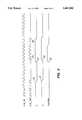
- FIG. 2illustrates a timing diagram which shows the timing of the operation of the low power clocking apparatus of the present invention.
- the output clock signal 24 from the multiplexer 4is illustrated at the top of FIG. 2 by the Clk -- in waveform
- the clock signal line 15 output from the inverter 28is illustrated as the Clk -- out waveform
- the D input to the flip-flop 22is illustrated as the D waveform
- the Q output from the D flip-flop 22is illustrated as the Q waveform
- the control line signal 8 from the comparison circuitry 2is illustrated as the Control waveform.
- the integrated circuit of the preferred embodimentUpon startup the integrated circuit of the preferred embodiment is brought up in its low power clock mode, with the clock signal 15 to the sub-circuits 11-14 disabled.
- the central arbiter 1pulls the Start -- Clock signal line 10 to a logical low voltage level, causing the Clk -- out signal to be activated and the clock signal 15 to be provided to the sub-circuits 11-14.
- the central arbiter 1will then raise the Start -- Clock signal line 10 to a logical high voltage level if the address specified on the system bus 9 is not within the range of addresses controlled by the central arbiter 1 and the command on the system bus 9 is not one of the specific commands that the central arbiter 1 is looking for.
- the sub-circuits 11-14have completed their required operations and no longer need the clock signal 15, they each raise their respective Kill -- Clock signal lines 16-19 to a logical high voltage level.
- the output 21 of the NAND gate 20 and the D input of the flip-flop 22switches from a logical high voltage level to a logical low voltage level as is illustrated in FIG. 2 at the time 50.
- the Q output of the flip-flop 22then switches from a logical high voltage level to a logical low voltage level on the next negative clock edge of the Clk -- in signal, illustrated in FIG. 2 at the time 51.
- the Clk -- out signalis disabled so that the sub-circuits 11-14 are not provided with a clock signal. Because the operation of the flip-flop 22 is controlled by the negative edge of the clock signal Clk -- in, the clock signal Clk -- out is disabled when it is already at a logical low voltage level, allowing disabling of the clock signal to occur without glitches or noise pulses.
- the central arbiter 1 and the comparison circuitry 2continuously monitor all of the addresses and commands on the system bus 9, until one of the addresses within the range controlled by the central arbiter 1 and one of the specific corresponding commands appears on the system bus 9.
- the central arbiter 1pulls the Start -- Clock signal line 10 to a logical low voltage level and the Clk -- out signal is re-enabled.
- the comparison circuitry 2raises the control signal line 8 to a logical high voltage level, as is illustrated at the time 52, notifying the central arbiter 1 an address within its control has been detected. If a corresponding command is also present on the system bus 9, the central arbiter 1 then pulls the Start -- Clock signal line 10 to a logical low voltage level and in response, the output 21 of the NAND gate 20 switches from a logical low voltage level to a logical high voltage level, causing the D input to the flip-flop 22 to do the same, as illustrated at the time 53 in FIG. 2.
- the Q output from the flip-flop 22switches from a logical low voltage level to a logical high voltage level, as illustrated at the time 54 in FIG. 2.
- the Clk -- out signalwill be re-enabled, beginning at the next positive clock edge as illustrated at the time 55. Because the clock signal Clk -- out is at a logical low voltage level when the clock signal is disabled, the present invention is designed so that the clock signal will always restart on the next positive edge of the clock signal Clk -- in.
- the signal Clk -- outstays enabled until the central arbiter 1 raises the Start -- Clock signal line 10 to a logical high voltage level and all of the sub-circuits 11-14 raise their respective Kill -- Clk signal lines 16-19 to a logical high voltage level, signalling that they all have completed their required operations and that they no longer require the clock signal 15.
- the output 21 of the NAND gate 20switches from a logical high voltage level to a logical low voltage level causing the D input of the flip-flop 22 to do the same.
- the Q outputis pulled to a logical low voltage level and the Clk -- out signal is disabled as illustrated in FIG. 2 at the time 56.
- the clockthen remains disabled until the central arbiter 1 pulls the Start -- Clock signal line 10 to a logical low voltage level.
- the clock signal 15 to the sub-circuits 11-14After the clock signal 15 to the sub-circuits 11-14 has been disabled, the clock signal 15 cannot be re-enabled and provided to those sub-circuits until the central arbiter 1 pulls the Start -- Clock signal line 10 to a logical low voltage level.
- the sub-circuits 11-14can only signal that they no longer require the clock signal 15, but cannot signal that they need the clock signal 15, once it has been disabled.
- the central arbiter 1must then monitor the system bus 9 and the comparison circuitry 2 so that it knows when the sub-circuits 11-14 are required for operation and will need the clock signal 15.
- the central arbiter 1 and the comparison circuitryIn order for the central arbiter 1 and the comparison circuitry to monitor the system bus, they must either be provided with a clock signal at all times or designed to be asynchronous.
- the output clock signal 24 from the multiplexer 4is always provided to the inverter 25, to the flip-flop 22 and to the NAND gate 26.
- the output clock signal 24 from the multiplexer 4is also coupled to always be provided to the central arbiter 1 for the parts of the central arbiter 1 which are synchronous and require the clock signal in order to monitor the system bus and the comparison circuitry.
- the comparison circuitry 2is designed to be asynchronous so that it does not require a clock signal to make its comparisons of the addresses on the system bus 9 and to notify the central arbiter 1 when the address on the system bus 9 is within the range of addresses controlled by the central arbiter 1.
- the preferred embodiment of the present inventionis incorporated within a PCMCIA Host Adapter.
- Appendix AAn Advance Data Sheet, dated October 1993, for PCMCIA Host Adapters, part Nos. CL-PD6710/PD672X, published by Cirrus Logic, Inc. of 3100 West Warren Ave., Fremont, Calif. 94538 which includes the low power clocking apparatus and method of the present invention, is included as Appendix A and attached hereto, beginning at page 12.
- Appendix BA VHDL code listing for the preferred embodiment of the central arbiter and the low power clocking apparatus is included as Appendix B and attached hereto as a microfiche appendix.
Landscapes
- Engineering & Computer Science (AREA)
- Theoretical Computer Science (AREA)
- General Engineering & Computer Science (AREA)
- Physics & Mathematics (AREA)
- General Physics & Mathematics (AREA)
- Computer Hardware Design (AREA)
- Computing Systems (AREA)
- Bus Control (AREA)
Abstract
Description
Claims (12)
Priority Applications (1)
| Application Number | Priority Date | Filing Date | Title |
|---|---|---|---|
| US08/149,107US5467042A (en) | 1993-11-08 | 1993-11-08 | Low power clocking apparatus and method |
Applications Claiming Priority (1)
| Application Number | Priority Date | Filing Date | Title |
|---|---|---|---|
| US08/149,107US5467042A (en) | 1993-11-08 | 1993-11-08 | Low power clocking apparatus and method |
Publications (1)
| Publication Number | Publication Date |
|---|---|
| US5467042Atrue US5467042A (en) | 1995-11-14 |
Family
ID=22528832
Family Applications (1)
| Application Number | Title | Priority Date | Filing Date |
|---|---|---|---|
| US08/149,107Expired - LifetimeUS5467042A (en) | 1993-11-08 | 1993-11-08 | Low power clocking apparatus and method |
Country Status (1)
| Country | Link |
|---|---|
| US (1) | US5467042A (en) |
Cited By (8)
| Publication number | Priority date | Publication date | Assignee | Title |
|---|---|---|---|---|
| US5675808A (en)* | 1994-11-02 | 1997-10-07 | Advanced Micro Devices, Inc. | Power control of circuit modules within an integrated circuit |
| US5886582A (en)* | 1996-08-07 | 1999-03-23 | Cypress Semiconductor Corp. | Enabling clock signals with a phase locked loop (PLL) lock detect circuit |
| US5907562A (en)* | 1996-07-31 | 1999-05-25 | Nokia Mobile Phones Limited | Testable integrated circuit with reduced power dissipation |
| US6272465B1 (en) | 1994-11-02 | 2001-08-07 | Legerity, Inc. | Monolithic PC audio circuit |
| US20050218957A1 (en)* | 2002-09-11 | 2005-10-06 | Haluk Konuk | Programmable frequency multiplier |
| WO2006131143A1 (en)* | 2005-06-10 | 2006-12-14 | Freescale Semiconductor, Inc. | Device and method for media access control |
| US20080155280A1 (en)* | 2006-12-22 | 2008-06-26 | Lance Hacking | Reducing idle leakage power in an ic |
| US20090175393A1 (en)* | 2005-06-10 | 2009-07-09 | Sanit-Gobain Glass France | Method and device for frame synchronization |
Citations (10)
| Publication number | Priority date | Publication date | Assignee | Title |
|---|---|---|---|---|
| US4218876A (en)* | 1976-11-29 | 1980-08-26 | Sharp Kabushiki Kaisha | Combined timekeeper and calculator with low power consumption features |
| US4317181A (en)* | 1979-12-26 | 1982-02-23 | Texas Instruments Incorporated | Four mode microcomputer power save operation |
| US4390022A (en)* | 1981-05-18 | 1983-06-28 | Intermedics, Inc. | Implantable device with microprocessor control |
| US4404972A (en)* | 1981-05-18 | 1983-09-20 | Intermedics, Inc. | Implantable device with microprocessor control |
| US4570219A (en)* | 1981-11-11 | 1986-02-11 | Hitachi, Ltd. | CMOS Circuit with reduced power dissipation and a digital data processor using the same |
| US4656649A (en)* | 1984-12-18 | 1987-04-07 | Nec Corporation | Clock frequency divider circuit |
| US4665536A (en)* | 1986-03-10 | 1987-05-12 | Burroughs Corporation | Programmable automatic power-off system for a digital terminal |
| US4731814A (en)* | 1986-02-21 | 1988-03-15 | AT&T Information Systems Inc. American Telephone & Telegraph Company | Computer-controlled cordless telephone |
| US5162667A (en)* | 1989-11-13 | 1992-11-10 | Mitsubishi Denki Kabushiki Kaisha | Semiconductor integrated circuit with master and slave latches |
| US5218704A (en)* | 1989-10-30 | 1993-06-08 | Texas Instruments | Real-time power conservation for portable computers |
- 1993
- 1993-11-08USUS08/149,107patent/US5467042A/ennot_activeExpired - Lifetime
Patent Citations (11)
| Publication number | Priority date | Publication date | Assignee | Title |
|---|---|---|---|---|
| US4218876A (en)* | 1976-11-29 | 1980-08-26 | Sharp Kabushiki Kaisha | Combined timekeeper and calculator with low power consumption features |
| US4317181A (en)* | 1979-12-26 | 1982-02-23 | Texas Instruments Incorporated | Four mode microcomputer power save operation |
| US4390022A (en)* | 1981-05-18 | 1983-06-28 | Intermedics, Inc. | Implantable device with microprocessor control |
| US4404972A (en)* | 1981-05-18 | 1983-09-20 | Intermedics, Inc. | Implantable device with microprocessor control |
| US4404972B1 (en)* | 1981-05-18 | 2000-07-11 | Intermedics Inc | Implantable device with microprocessor control |
| US4570219A (en)* | 1981-11-11 | 1986-02-11 | Hitachi, Ltd. | CMOS Circuit with reduced power dissipation and a digital data processor using the same |
| US4656649A (en)* | 1984-12-18 | 1987-04-07 | Nec Corporation | Clock frequency divider circuit |
| US4731814A (en)* | 1986-02-21 | 1988-03-15 | AT&T Information Systems Inc. American Telephone & Telegraph Company | Computer-controlled cordless telephone |
| US4665536A (en)* | 1986-03-10 | 1987-05-12 | Burroughs Corporation | Programmable automatic power-off system for a digital terminal |
| US5218704A (en)* | 1989-10-30 | 1993-06-08 | Texas Instruments | Real-time power conservation for portable computers |
| US5162667A (en)* | 1989-11-13 | 1992-11-10 | Mitsubishi Denki Kabushiki Kaisha | Semiconductor integrated circuit with master and slave latches |
Non-Patent Citations (16)
| Title |
|---|
| "Cirrus Logic Enters PCMCIA World with Industry-Leading Host Adapter, Disk Drive Controllers" Press Release made by Cirrus Logic, Inc., Sep. 28, 1992. |
| "CL-PD6710 & CL-PD6720 Advanced Data Sheet", Revision 1.0.1, Published by Cirrus Logic, Inc., Jul. 23, 1992. |
| "CL-PD6710 & CL-PD6720 Advanced Data Sheet", Revision 1.0.2, Published by Cirrus Logic, Inc., Jul. 30, 1992. |
| "CL-PD6710 & CL-PD6720 Advanced Data Sheet", Revision 1.0.3, Published by Cirrus Logic, Inc., Sep. 1, 1992. |
| "CL-PD6710 & CL-PD6720 Advanced Data Sheet", Revision 1.0.3, Published by Cirrus Logic, Inc., Sep. 2, 1992. |
| "CL-PD6710 & CL-PD6720 Advanced Data Sheet", Revision 1.0.4, Published by Cirrus Logic, Inc., Oct. 20, 1992. |
| "CL-PD6710/6720 Advanced Product Bulletin", by Cirrus Logic, Inc., Sep. 1992. |
| "Personal Computer Memory Card International Association Standards", Release 2.01, published by Personal Computer Memory Card International Association, 1030G East Duane Avenue, Sunnyvale, Calif. 94086, Nov. 1992. |
| Cirrus Logic Enters PCMCIA World with Industry Leading Host Adapter, Disk Drive Controllers Press Release made by Cirrus Logic, Inc., Sep. 28, 1992.* |
| CL PD6710 & CL PD6720 Advanced Data Sheet , Revision 1.0.1, Published by Cirrus Logic, Inc., Jul. 23, 1992.* |
| CL PD6710 & CL PD6720 Advanced Data Sheet , Revision 1.0.2, Published by Cirrus Logic, Inc., Jul. 30, 1992.* |
| CL PD6710 & CL PD6720 Advanced Data Sheet , Revision 1.0.3, Published by Cirrus Logic, Inc., Sep. 1, 1992.* |
| CL PD6710 & CL PD6720 Advanced Data Sheet , Revision 1.0.3, Published by Cirrus Logic, Inc., Sep. 2, 1992.* |
| CL PD6710 & CL PD6720 Advanced Data Sheet , Revision 1.0.4, Published by Cirrus Logic, Inc., Oct. 20, 1992.* |
| CL PD6710/6720 Advanced Product Bulletin , by Cirrus Logic, Inc., Sep. 1992.* |
| Personal Computer Memory Card International Association Standards , Release 2.01, published by Personal Computer Memory Card International Association, 1030G East Duane Avenue, Sunnyvale, Calif. 94086, Nov. 1992.* |
Cited By (14)
| Publication number | Priority date | Publication date | Assignee | Title |
|---|---|---|---|---|
| US6272465B1 (en) | 1994-11-02 | 2001-08-07 | Legerity, Inc. | Monolithic PC audio circuit |
| US5675808A (en)* | 1994-11-02 | 1997-10-07 | Advanced Micro Devices, Inc. | Power control of circuit modules within an integrated circuit |
| US5907562A (en)* | 1996-07-31 | 1999-05-25 | Nokia Mobile Phones Limited | Testable integrated circuit with reduced power dissipation |
| US5886582A (en)* | 1996-08-07 | 1999-03-23 | Cypress Semiconductor Corp. | Enabling clock signals with a phase locked loop (PLL) lock detect circuit |
| US20050218957A1 (en)* | 2002-09-11 | 2005-10-06 | Haluk Konuk | Programmable frequency multiplier |
| US8223910B2 (en) | 2005-06-10 | 2012-07-17 | Freescale Semiconductor, Inc. | Method and device for frame synchronization |
| WO2006131143A1 (en)* | 2005-06-10 | 2006-12-14 | Freescale Semiconductor, Inc. | Device and method for media access control |
| US9047415B2 (en) | 2005-06-10 | 2015-06-02 | Freescale Semiconductor, Inc. | Device and method for media access control |
| US20090175393A1 (en)* | 2005-06-10 | 2009-07-09 | Sanit-Gobain Glass France | Method and device for frame synchronization |
| US20080155280A1 (en)* | 2006-12-22 | 2008-06-26 | Lance Hacking | Reducing idle leakage power in an ic |
| GB2456993A (en)* | 2006-12-22 | 2009-08-05 | Intel Corp | Reducing idle leakage power in an IC |
| GB2456993B (en)* | 2006-12-22 | 2012-09-19 | Intel Corp | Reducing idle leakage power in an IC |
| US8392728B2 (en) | 2006-12-22 | 2013-03-05 | Intel Corporation | Reducing idle leakage power in an IC |
| WO2008079518A1 (en)* | 2006-12-22 | 2008-07-03 | Intel Corporation | Reducing idle leakage power in an ic |
Similar Documents
| Publication | Publication Date | Title |
|---|---|---|
| US5677849A (en) | Selective low power clocking apparatus and method | |
| US7594126B2 (en) | Processor system and method for reducing power consumption in idle mode | |
| EP1451666B1 (en) | Glitch free clock selection switch | |
| US6397338B2 (en) | Power management circuit that qualifies powergood disposal signal | |
| US6639454B2 (en) | Multiple circuit blocks with interblock control and power conservation | |
| US5898232A (en) | Input/output section of an integrated circuit having separate power down capability | |
| US6501304B1 (en) | Glitch-less clock selector | |
| WO1999066640A1 (en) | Semiconductor integrated circuit | |
| US7103785B2 (en) | Method and apparatus for power management event wake up | |
| US5384747A (en) | Circuit for placing a memory device into low power mode | |
| US7263120B2 (en) | Semiconductor device to reduce power individually to each circuit | |
| EP0834105B1 (en) | Wake-up system for a pcmcia card | |
| US5548250A (en) | Low power phase lock loop clocking circuit for battery powered systems | |
| US5467042A (en) | Low power clocking apparatus and method | |
| JP3070527B2 (en) | Wireless mobile terminal | |
| US5410712A (en) | Computer system equipped with extended unit including power supply | |
| KR20160143159A (en) | Power Gating Control Circuit For Controlling Stably Data Restoring | |
| US4722070A (en) | Multiple oscillation switching circuit | |
| US6292038B1 (en) | Smooth clock switching for power managed PCI adapters | |
| US5587675A (en) | Multiclock controller | |
| US6959396B2 (en) | Method and apparatus for reducing clock skew in an integrated circuit | |
| US6853929B2 (en) | Pipeline control for power management | |
| KR100616683B1 (en) | Power-Down and Wake-Up Circuitry | |
| JPH10133766A (en) | Adaptive power-down clock control | |
| EP0621526A1 (en) | Method and apparatus for powering up and powering down peripheral elements |
Legal Events
| Date | Code | Title | Description |
|---|---|---|---|
| AS | Assignment | Owner name:CIRRUS LOGIC, INC., CALIFORNIA Free format text:ASSIGNMENT OF ASSIGNORS INTEREST;ASSIGNORS:SMITH, STEPHEN A.;RICHTER, BRIAN;SINGHAL, DAVE M.;REEL/FRAME:006864/0851;SIGNING DATES FROM 19931215 TO 19931216 | |
| STCF | Information on status: patent grant | Free format text:PATENTED CASE | |
| AS | Assignment | Owner name:BANK OF AMERICA NATIONAL TRUST & SAVINGS ASSOCIATI Free format text:SECURITY INTEREST;ASSIGNOR:CIRRUS LOGIC, INC.;REEL/FRAME:007986/0917 Effective date:19960430 | |
| FEPP | Fee payment procedure | Free format text:PAYOR NUMBER ASSIGNED (ORIGINAL EVENT CODE: ASPN); ENTITY STATUS OF PATENT OWNER: LARGE ENTITY | |
| FPAY | Fee payment | Year of fee payment:4 | |
| AS | Assignment | Owner name:CIRRUS LOGIC INTERNATIONAL LTD., BERMUDA Free format text:DEED OF DISCHARGE;ASSIGNOR:BANK OF AMERICA NATIONAL TRUST SAVINGS ASSOCIATION;REEL/FRAME:013782/0435 Effective date:19970630 | |
| FPAY | Fee payment | Year of fee payment:8 | |
| FPAY | Fee payment | Year of fee payment:12 |