US5466639A - Double mask process for forming trenches and contacts during the formation of a semiconductor memory device - Google Patents
Double mask process for forming trenches and contacts during the formation of a semiconductor memory deviceDownload PDFInfo
- Publication number
- US5466639A US5466639AUS08/319,217US31921794AUS5466639AUS 5466639 AUS5466639 AUS 5466639AUS 31921794 AUS31921794 AUS 31921794AUS 5466639 AUS5466639 AUS 5466639A
- Authority
- US
- United States
- Prior art keywords
- layer
- forming
- mask
- over
- conductive
- Prior art date
- Legal status (The legal status is an assumption and is not a legal conclusion. Google has not performed a legal analysis and makes no representation as to the accuracy of the status listed.)
- Expired - Lifetime
Links
- 238000000034methodMethods0.000titleclaimsabstractdescription31
- 239000004065semiconductorSubstances0.000titleclaimsabstractdescription19
- 230000015572biosynthetic processEffects0.000titleclaimsdescription8
- 229910052751metalInorganic materials0.000claimsdescription18
- 239000002184metalSubstances0.000claimsdescription18
- 238000005530etchingMethods0.000claimsdescription7
- 229910052581Si3N4Inorganic materials0.000claimsdescription5
- HQVNEWCFYHHQES-UHFFFAOYSA-Nsilicon nitrideChemical groupN12[Si]34N5[Si]62N3[Si]51N64HQVNEWCFYHHQES-UHFFFAOYSA-N0.000claimsdescription5
- 238000000059patterningMethods0.000claimsdescription4
- 239000010410layerSubstances0.000claims54
- 239000002356single layerSubstances0.000claims1
- 239000000758substrateSubstances0.000abstractdescription16
- 239000003989dielectric materialSubstances0.000description3
- 239000000463materialSubstances0.000description3
- 229920002120photoresistant polymerPolymers0.000description3
- 239000005380borophosphosilicate glassSubstances0.000description2
- 239000004020conductorSubstances0.000description2
- 238000012986modificationMethods0.000description2
- 230000004048modificationEffects0.000description2
- JBRZTFJDHDCESZ-UHFFFAOYSA-NAsGaChemical compound[As]#[Ga]JBRZTFJDHDCESZ-UHFFFAOYSA-N0.000description1
- 229910001218Gallium arsenideInorganic materials0.000description1
- 230000008021depositionEffects0.000description1
- 238000004519manufacturing processMethods0.000description1
- -1masksSubstances0.000description1
- 150000002739metalsChemical class0.000description1
- 229910021420polycrystalline siliconInorganic materials0.000description1
- 229910052710siliconInorganic materials0.000description1
- 239000010703siliconSubstances0.000description1
- 239000000126substanceSubstances0.000description1
Images


Classifications
- H—ELECTRICITY
- H01—ELECTRIC ELEMENTS
- H01L—SEMICONDUCTOR DEVICES NOT COVERED BY CLASS H10
- H01L21/00—Processes or apparatus adapted for the manufacture or treatment of semiconductor or solid state devices or of parts thereof
- H01L21/70—Manufacture or treatment of devices consisting of a plurality of solid state components formed in or on a common substrate or of parts thereof; Manufacture of integrated circuit devices or of parts thereof
- H01L21/71—Manufacture of specific parts of devices defined in group H01L21/70
- H01L21/768—Applying interconnections to be used for carrying current between separate components within a device comprising conductors and dielectrics
- H01L21/76801—Applying interconnections to be used for carrying current between separate components within a device comprising conductors and dielectrics characterised by the formation and the after-treatment of the dielectrics, e.g. smoothing
- H01L21/76802—Applying interconnections to be used for carrying current between separate components within a device comprising conductors and dielectrics characterised by the formation and the after-treatment of the dielectrics, e.g. smoothing by forming openings in dielectrics
- H01L21/76807—Applying interconnections to be used for carrying current between separate components within a device comprising conductors and dielectrics characterised by the formation and the after-treatment of the dielectrics, e.g. smoothing by forming openings in dielectrics for dual damascene structures
- H01L21/7681—Applying interconnections to be used for carrying current between separate components within a device comprising conductors and dielectrics characterised by the formation and the after-treatment of the dielectrics, e.g. smoothing by forming openings in dielectrics for dual damascene structures involving one or more buried masks
- Y—GENERAL TAGGING OF NEW TECHNOLOGICAL DEVELOPMENTS; GENERAL TAGGING OF CROSS-SECTIONAL TECHNOLOGIES SPANNING OVER SEVERAL SECTIONS OF THE IPC; TECHNICAL SUBJECTS COVERED BY FORMER USPC CROSS-REFERENCE ART COLLECTIONS [XRACs] AND DIGESTS
- Y10—TECHNICAL SUBJECTS COVERED BY FORMER USPC
- Y10S—TECHNICAL SUBJECTS COVERED BY FORMER USPC CROSS-REFERENCE ART COLLECTIONS [XRACs] AND DIGESTS
- Y10S148/00—Metal treatment
- Y10S148/106—Masks, special
- Y—GENERAL TAGGING OF NEW TECHNOLOGICAL DEVELOPMENTS; GENERAL TAGGING OF CROSS-SECTIONAL TECHNOLOGIES SPANNING OVER SEVERAL SECTIONS OF THE IPC; TECHNICAL SUBJECTS COVERED BY FORMER USPC CROSS-REFERENCE ART COLLECTIONS [XRACs] AND DIGESTS
- Y10—TECHNICAL SUBJECTS COVERED BY FORMER USPC
- Y10S—TECHNICAL SUBJECTS COVERED BY FORMER USPC CROSS-REFERENCE ART COLLECTIONS [XRACs] AND DIGESTS
- Y10S438/00—Semiconductor device manufacturing: process
- Y10S438/942—Masking
- Y10S438/945—Special, e.g. metal
- Y—GENERAL TAGGING OF NEW TECHNOLOGICAL DEVELOPMENTS; GENERAL TAGGING OF CROSS-SECTIONAL TECHNOLOGIES SPANNING OVER SEVERAL SECTIONS OF THE IPC; TECHNICAL SUBJECTS COVERED BY FORMER USPC CROSS-REFERENCE ART COLLECTIONS [XRACs] AND DIGESTS
- Y10—TECHNICAL SUBJECTS COVERED BY FORMER USPC
- Y10S—TECHNICAL SUBJECTS COVERED BY FORMER USPC CROSS-REFERENCE ART COLLECTIONS [XRACs] AND DIGESTS
- Y10S438/00—Semiconductor device manufacturing: process
- Y10S438/975—Substrate or mask aligning feature
Definitions
- This inventionrelates to the field of semiconductor manufacture, and more specifically to the formation of contacts and trenches in a dielectric material.
- layers of various materialssuch as dielectrics, masks, metals, doped polycrystalline silicon, and photoresist are formed over a semiconductor substrate.
- Contacts through dielectric materials to the semiconductor substrateare typically required during the formation of semiconductor devices, such as memory devices and microprocessors. Contacts to features other than the substrate, such as word lines and other structures, are also commonly performed.
- One process to form a contact to a semiconductor substrate or other features through a dielectricincludes the step of forming a dielectric layer over the semiconductor substrate, then forming a first patterned layer of photoresist (resist) over the dielectric. An etch defines a contact through the dielectric to the substrate, and the resist layer is then removed.
- the contactsare often connected with word lines or bit lines.
- a second layer of resistis patterned over the dielectric layer leaving the contacts exposed, and also leaving exposed an area parallel and overlying the contacts.
- the dielectricis again etched, although the dielectric is not etched completely, thereby creating a trench in the dielectric but no additional contacts to the substrate.
- a layer of conductive materialsuch as metal is then blanket deposited over the surface of the dielectric, and the wafer is planarized to leave conductive material within the contacts and within the trench.
- One problemis that the dielectric is etched to expose the substrate, then a second patterned resist layer is subsequently formed over the dielectric thus filling the contacts with resist. Due to the small sizes of the contacts in the dielectric, it can be difficult to completely remove the resist from the contacts in the dielectric, and thus the conductive layer which contacts the substrate may not make adequate electrical contact.
- One method to solve the problem associated with resist filling the contacthas been to first etch a contact in a first dielectric layer, then to deposit and planarize a first metal layer to form a metal plug to the substrate.
- a second dielectric layer having a trenchis patterned over the first metal layer and over the first dielectric layer, then a second metal layer is formed over the second dielectric layer and then planarized.
- This processrequires the formation and planarization of two metal layers, thus adding additional steps and an additional metal-to-metal interface, which can be difficult to form reliably.
- a process which can be accomplished by the deposition of a single metal layer and does not require the formation of a resist layer within the contact to the substratewould be desirable.
- a method of forming a semiconductor devicecomprises the steps of forming a first dielectric layer over a feature such as a semiconductor substrate or a conductive line or plate, then forming a hard mask over the first dielectric layer.
- a first patterned resist layeris formed directly on the hard mask, and the hard mask is patterned using the first resist layer as a pattern. The first resist layer is removed.
- a second dielectricis formed over the hard mask, and a second patterned resist layer is formed over the second dielectric layer.
- the second dielectric layeris etched using the second resist layer as a pattern.
- the first dielectric layeris etched using the hard mask as a pattern.
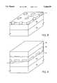
- FIGS. 1-8are isometric views showing one possible embodiment of the inventive process.
- a method of forming a semiconductor devicecomprises the steps of forming a first dielectric layer 10, such as an oxide such as borophosphosilicate glass (BPSG), over a semiconductor substrate 12 such as a wafer of silicon or gallium arsenide.
- a hard mask 14, such as a thermal layer of silicon nitride,is then formed over the first dielectric layer 10.
- a hard maskfor purposes of this disclosure, is a layer which can be etched selective to the underlying dielectric layer. Various materials other than thermal silicon nitride may be used for the hard mask.
- a first patterned layer of photoresist (resist) 16 having contact locations 18is formed on the hard mask 14, and the hard mask is patterned using the first resist layer as a pattern as shown in FIG. 2 which leaves the contact locations 18 etched in the hard mask 14.
- the patterning of the hard mask 14can be accomplished by any means which removes the hard mask and leaves the underlying dielectric layer substantially intact. Either a wet or dry etch using materials known in the art would be sufficient, depending on the hard mask and the dielectric layers used.
- the first resist layer 16is then stripped as shown in FIG. 3.
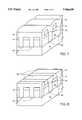
- a second dielectric layer 40is formed over the hard mask 14, and a second resist layer 42 is formed over the second dielectric layer 40.
- the resist 42is patterned and the second dielectric layer 40 is etched using the second resist layer 42 as a pattern, which forms a trench 50 in the second dielectric layer 40.
- the hard mask 14functions as an etch stop layer, thereby preventing the trench 50 from being etched into the first dielectric layer 10.
- the first dielectric layer 10is then etched using the hard mask 14 as a pattern to form a contact 52 in the first dielectric layer 10 to the substrate 12.
- the etching of the first 10 and second 40 dielectric layerscan be performed during two different etch steps, or it may be preferable to etch the two layers during a single etch step.
- the second resist layer 42is removed as shown in FIG. 6, and, referring to FIG. 7, a conductive layer 70 (including any adhesion layers, not shown, required to adhere the conductive layer to the underlying layer), such as a metal layer is formed over the hard mask 14 and over the first 10 and second 40 dielectric layers.
- the conductive layer 70fills the contact 52 in the first dielectric layer 10 and the trench 50 in the second dielectric layer 40. Planarizing the conductive layer 70 electrically isolates one trench from the next, to form conductive lines 80 such as word lines or bit lines as shown in FIG. 8.
- the conductive layercan be planarized by any workable means, such as by chemical mechanical polish, a dry etch, etc.
Landscapes
- Engineering & Computer Science (AREA)
- Physics & Mathematics (AREA)
- Condensed Matter Physics & Semiconductors (AREA)
- General Physics & Mathematics (AREA)
- Manufacturing & Machinery (AREA)
- Computer Hardware Design (AREA)
- Microelectronics & Electronic Packaging (AREA)
- Power Engineering (AREA)
- Internal Circuitry In Semiconductor Integrated Circuit Devices (AREA)
Abstract
Description
Claims (20)
Priority Applications (3)
| Application Number | Priority Date | Filing Date | Title |
|---|---|---|---|
| US08/319,217US5466639A (en) | 1994-10-06 | 1994-10-06 | Double mask process for forming trenches and contacts during the formation of a semiconductor memory device |
| US08/556,345US6165889A (en) | 1994-10-06 | 1995-11-13 | Process for forming trenches and contacts during the formation of a semiconductor memory device |
| US09/746,899US6420257B2 (en) | 1994-10-06 | 2000-12-22 | Process for forming trenches and contacts during the formation of a semiconductor memory device |
Applications Claiming Priority (1)
| Application Number | Priority Date | Filing Date | Title |
|---|---|---|---|
| US08/319,217US5466639A (en) | 1994-10-06 | 1994-10-06 | Double mask process for forming trenches and contacts during the formation of a semiconductor memory device |
Related Child Applications (1)
| Application Number | Title | Priority Date | Filing Date |
|---|---|---|---|
| US08/556,345ContinuationUS6165889A (en) | 1994-10-06 | 1995-11-13 | Process for forming trenches and contacts during the formation of a semiconductor memory device |
Publications (1)
| Publication Number | Publication Date |
|---|---|
| US5466639Atrue US5466639A (en) | 1995-11-14 |
Family
ID=23241340
Family Applications (3)
| Application Number | Title | Priority Date | Filing Date |
|---|---|---|---|
| US08/319,217Expired - LifetimeUS5466639A (en) | 1994-10-06 | 1994-10-06 | Double mask process for forming trenches and contacts during the formation of a semiconductor memory device |
| US08/556,345Expired - LifetimeUS6165889A (en) | 1994-10-06 | 1995-11-13 | Process for forming trenches and contacts during the formation of a semiconductor memory device |
| US09/746,899Expired - LifetimeUS6420257B2 (en) | 1994-10-06 | 2000-12-22 | Process for forming trenches and contacts during the formation of a semiconductor memory device |
Family Applications After (2)
| Application Number | Title | Priority Date | Filing Date |
|---|---|---|---|
| US08/556,345Expired - LifetimeUS6165889A (en) | 1994-10-06 | 1995-11-13 | Process for forming trenches and contacts during the formation of a semiconductor memory device |
| US09/746,899Expired - LifetimeUS6420257B2 (en) | 1994-10-06 | 2000-12-22 | Process for forming trenches and contacts during the formation of a semiconductor memory device |
Country Status (1)
| Country | Link |
|---|---|
| US (3) | US5466639A (en) |
Cited By (42)
| Publication number | Priority date | Publication date | Assignee | Title |
|---|---|---|---|---|
| US5705430A (en)* | 1995-06-07 | 1998-01-06 | Advanced Micro Devices, Inc. | Dual damascene with a sacrificial via fill |
| US5736457A (en)* | 1994-12-09 | 1998-04-07 | Sematech | Method of making a damascene metallization |
| US5801094A (en)* | 1997-02-28 | 1998-09-01 | United Microelectronics Corporation | Dual damascene process |
| US5821169A (en)* | 1996-08-05 | 1998-10-13 | Sharp Microelectronics Technology,Inc. | Hard mask method for transferring a multi-level photoresist pattern |
| GB2325083A (en)* | 1997-05-09 | 1998-11-11 | United Microelectronics Corp | A dual damascene process |
| US5863835A (en)* | 1996-12-30 | 1999-01-26 | Samsung Electronics Co., Ltd. | Methods of forming electrical interconnects on semiconductor substrates |
| US5886410A (en)* | 1996-06-26 | 1999-03-23 | Intel Corporation | Interconnect structure with hard mask and low dielectric constant materials |
| US5897366A (en)* | 1997-03-10 | 1999-04-27 | Motorola, Inc. | Method of resistless gate metal etch for fets |
| US5932928A (en)* | 1997-07-03 | 1999-08-03 | Micron Technology, Inc. | Semiconductor circuit interconnections and methods of making such interconnections |
| US5960304A (en)* | 1996-05-20 | 1999-09-28 | Texas Instruments Incorporated | Method for forming a contact to a substrate |
| US5981374A (en)* | 1997-04-29 | 1999-11-09 | International Business Machines Corporation | Sub-half-micron multi-level interconnection structure and process thereof |
| US5990015A (en)* | 1997-12-20 | 1999-11-23 | United Microelectronics Corp. | Dual damascence process |
| US6004883A (en)* | 1998-10-23 | 1999-12-21 | Taiwan Semiconductor Manufacturing Company, Ltd. | Dual damascene patterned conductor layer formation method without etch stop layer |
| US6037262A (en)* | 1998-06-15 | 2000-03-14 | Lsi Logic Corporation | Process for forming vias, and trenches for metal lines, in multiple dielectric layers of integrated circuit structure |
| US6081033A (en)* | 1997-07-29 | 2000-06-27 | Micron Technology, Inc. | Interconnections for semiconductor circuits |
| US6096660A (en)* | 1997-08-21 | 2000-08-01 | Micron Technology, Inc. | Method for removing undesirable second oxide while minimally affecting a desirable first oxide |
| US6133139A (en)* | 1997-10-08 | 2000-10-17 | International Business Machines Corporation | Self-aligned composite insulator with sub-half-micron multilevel high density electrical interconnections and process thereof |
| US6136686A (en)* | 1997-07-18 | 2000-10-24 | International Business Machines Corporation | Fabrication of interconnects with two different thicknesses |
| US6140220A (en)* | 1999-07-08 | 2000-10-31 | Industrial Technology Institute Reseach | Dual damascene process and structure with dielectric barrier layer |
| US6204166B1 (en) | 1998-08-21 | 2001-03-20 | Micron Technology, Inc. | Method for forming dual damascene structures |
| US6271593B1 (en)* | 1997-08-21 | 2001-08-07 | Micron Technology, Inc. | Method for fabricating conductive components in microelectronic devices and substrate structures therefor |
| US6295721B1 (en)* | 1999-12-28 | 2001-10-02 | Taiwan Semiconductor Manufacturing Company | Metal fuse in copper dual damascene |
| US20020093058A1 (en)* | 1998-09-03 | 2002-07-18 | Mcqueen Mark | Esd/eos protection structure for integrated circuit devices |
| US6440858B1 (en) | 1998-08-24 | 2002-08-27 | International Business Machines Corporation | Multi-layer hard mask for deep trench silicon etch |
| US6461963B1 (en) | 2000-08-30 | 2002-10-08 | Micron Technology, Inc. | Utilization of disappearing silicon hard mask for fabrication of semiconductor structures |
| US20030061958A1 (en)* | 2001-10-02 | 2003-04-03 | Guobiao Zhang | Low-cost lithography |
| US6551894B1 (en)* | 1995-09-29 | 2003-04-22 | Kabushiki Kaisha Toshiba | Stacked capacitor-type semiconductor storage device and manufacturing method thereof |
| DE10200428A1 (en)* | 2002-01-09 | 2003-04-30 | Infineon Technologies Ag | Production of contact structures in a metallizing on a semiconductor wafer comprises preparing a wafer having an active region, applying a first insulating layer on the wafer |
| US20030087167A1 (en)* | 2001-11-08 | 2003-05-08 | Martin Popp | Method for fabricating a mask for semiconductor structures |
| US6593223B1 (en) | 1998-06-01 | 2003-07-15 | United Microelectronics Corporation | Method of forming dual damascene structure |
| US6620739B1 (en)* | 1999-03-09 | 2003-09-16 | Tokyo Electron Limited | Method of manufacturing semiconductor device |
| EP0905774A3 (en)* | 1997-09-30 | 2003-11-19 | Infineon Technologies AG | Soft passivation layer in semiconductor fabrication |
| US6680248B2 (en) | 1998-06-01 | 2004-01-20 | United Microelectronics Corporation | Method of forming dual damascene structure |
| US20040041185A1 (en)* | 2002-08-29 | 2004-03-04 | Micron Technology, Inc. | Self-aligned, integrated circuit contact and formation method |
| DE10240099A1 (en)* | 2002-08-30 | 2004-03-11 | Infineon Technologies Ag | Production of a semiconductor structure comprises preparing a semiconductor substrate, providing a lower first, a middle second and an upper third mask layer on a surface of the substrate, and further processing |
| US20040097013A1 (en)* | 2002-11-15 | 2004-05-20 | Water Lur | Air gap structure and formation method for reducing undesired capacitive coupling between interconnects in an integrated circuit device |
| US20040094821A1 (en)* | 2002-11-15 | 2004-05-20 | Water Lur | Air gap for dual damascene applications |
| US20040097065A1 (en)* | 2002-11-15 | 2004-05-20 | Water Lur | Air gap for tungsten/aluminum plug applications |
| US6743711B2 (en) | 2001-06-27 | 2004-06-01 | Hynix Semiconductor Inc. | Method for forming dual damascene line structure |
| US20050250315A1 (en)* | 2004-05-06 | 2005-11-10 | Tran Luan C | Methods of forming electrical connections for semiconductor constructions |
| KR101145336B1 (en) | 2010-05-31 | 2012-05-14 | 에스케이하이닉스 주식회사 | Method for fabricating contact hole in semiconductor device |
| US8823119B2 (en) | 2012-03-09 | 2014-09-02 | Samsung Electronics Co., Ltd. | Magnetic device having a metallic glass alloy |
Families Citing this family (5)
| Publication number | Priority date | Publication date | Assignee | Title |
|---|---|---|---|---|
| JP2004356469A (en)* | 2003-05-30 | 2004-12-16 | Renesas Technology Corp | Manufacturing method of semiconductor integrated circuit device |
| US7381654B2 (en)* | 2005-05-31 | 2008-06-03 | Taiwan Semiconductor Manufacturing Co. | Method for fabricating right-angle holes in a substrate |
| JP4155587B2 (en)* | 2006-04-06 | 2008-09-24 | 株式会社東芝 | Manufacturing method of semiconductor device |
| US7833893B2 (en)* | 2007-07-10 | 2010-11-16 | International Business Machines Corporation | Method for forming conductive structures |
| US8647981B1 (en)* | 2012-08-31 | 2014-02-11 | Micron Technology, Inc. | Methods of forming patterns, and methods of forming integrated circuitry |
Citations (5)
| Publication number | Priority date | Publication date | Assignee | Title |
|---|---|---|---|---|
| US4997789A (en)* | 1988-10-31 | 1991-03-05 | Texas Instruments Incorporated | Aluminum contact etch mask and etchstop for tungsten etchback |
| US5055423A (en)* | 1987-12-28 | 1991-10-08 | Texas Instruments Incorporated | Planarized selective tungsten metallization system |
| US5354711A (en)* | 1990-06-26 | 1994-10-11 | Commissariat A L'energie Atomique | Process for etching and depositing integrated circuit interconnections and contacts |
| US5397908A (en)* | 1993-06-09 | 1995-03-14 | Micron Technology, Inc. | Arrays of memory integrated circuitry |
| US5403781A (en)* | 1992-07-17 | 1995-04-04 | Yamaha Corporation | Method of forming multilayered wiring |
Family Cites Families (3)
| Publication number | Priority date | Publication date | Assignee | Title |
|---|---|---|---|---|
| FR2664095B1 (en)* | 1990-06-28 | 1993-12-17 | Commissariat A Energie Atomique | METHOD FOR MANUFACTURING AN ELECTRICAL CONTACT ON AN ACTIVE ELEMENT OF A MIS INTEGRATED CIRCUIT. |
| KR960002064B1 (en)* | 1992-11-16 | 1996-02-10 | 현대전자산업주식회사 | Contact manufacturing method of semiconductor device |
| KR100256800B1 (en)* | 1993-06-22 | 2000-05-15 | 김영환 | Method of forming contact hole |
- 1994
- 1994-10-06USUS08/319,217patent/US5466639A/ennot_activeExpired - Lifetime
- 1995
- 1995-11-13USUS08/556,345patent/US6165889A/ennot_activeExpired - Lifetime
- 2000
- 2000-12-22USUS09/746,899patent/US6420257B2/ennot_activeExpired - Lifetime
Patent Citations (5)
| Publication number | Priority date | Publication date | Assignee | Title |
|---|---|---|---|---|
| US5055423A (en)* | 1987-12-28 | 1991-10-08 | Texas Instruments Incorporated | Planarized selective tungsten metallization system |
| US4997789A (en)* | 1988-10-31 | 1991-03-05 | Texas Instruments Incorporated | Aluminum contact etch mask and etchstop for tungsten etchback |
| US5354711A (en)* | 1990-06-26 | 1994-10-11 | Commissariat A L'energie Atomique | Process for etching and depositing integrated circuit interconnections and contacts |
| US5403781A (en)* | 1992-07-17 | 1995-04-04 | Yamaha Corporation | Method of forming multilayered wiring |
| US5397908A (en)* | 1993-06-09 | 1995-03-14 | Micron Technology, Inc. | Arrays of memory integrated circuitry |
Non-Patent Citations (4)
| Title |
|---|
| Kaanta et al., "Dual Damascene: A ULSI Wiring Technology", Jun. 11-12, 1991 IEEE, VMIC Conference, pp. 144-152. |
| Kaanta et al., Dual Damascene: A ULSI Wiring Technology , Jun. 11 12, 1991 IEEE, VMIC Conference, pp. 144 152.* |
| Ueno et al, "A Quarter-Micron Planarized Interconnection Technology with Self-Aligned Plug", Apr. 1992 IEEE, pp. 305-308. |
| Ueno et al, A Quarter Micron Planarized Interconnection Technology with Self Aligned Plug , Apr. 1992 IEEE, pp. 305 308.* |
Cited By (79)
| Publication number | Priority date | Publication date | Assignee | Title |
|---|---|---|---|---|
| US6445073B1 (en) | 1994-12-09 | 2002-09-03 | Newport Fab, Llc | Damascene metallization process and structure |
| US5736457A (en)* | 1994-12-09 | 1998-04-07 | Sematech | Method of making a damascene metallization |
| US5705430A (en)* | 1995-06-07 | 1998-01-06 | Advanced Micro Devices, Inc. | Dual damascene with a sacrificial via fill |
| US7187027B2 (en) | 1995-09-29 | 2007-03-06 | Kabushiki Kaisha Toshiba | Stacked capacitor-type semiconductor storage device and manufacturing method thereof |
| US6846733B2 (en) | 1995-09-29 | 2005-01-25 | Kabushiki Kaisha Toshiba | Stacked capacitor-type semiconductor storage device and manufacturing method thereof |
| US20030178686A1 (en)* | 1995-09-29 | 2003-09-25 | Kabushiki Kaisha Toshiba | Stacked capacitor-type semiconductor storage device and manufacturing method thereof |
| US6551894B1 (en)* | 1995-09-29 | 2003-04-22 | Kabushiki Kaisha Toshiba | Stacked capacitor-type semiconductor storage device and manufacturing method thereof |
| US7023044B2 (en) | 1995-09-29 | 2006-04-04 | Kabushiki Kaisha Toshiba | Stacked capacitor-type semiconductor storage device and manufacturing method thereof |
| US20060124980A1 (en)* | 1995-09-29 | 2006-06-15 | Kabushiki Kaisha Toshiba | Stacked capacitor-type semiconductor storage device and manufacturing method thereof |
| US5960304A (en)* | 1996-05-20 | 1999-09-28 | Texas Instruments Incorporated | Method for forming a contact to a substrate |
| US6027995A (en)* | 1996-06-26 | 2000-02-22 | Intel Corporation | Method for fabricating an interconnect structure with hard mask and low dielectric constant materials |
| US5886410A (en)* | 1996-06-26 | 1999-03-23 | Intel Corporation | Interconnect structure with hard mask and low dielectric constant materials |
| US5821169A (en)* | 1996-08-05 | 1998-10-13 | Sharp Microelectronics Technology,Inc. | Hard mask method for transferring a multi-level photoresist pattern |
| US5863835A (en)* | 1996-12-30 | 1999-01-26 | Samsung Electronics Co., Ltd. | Methods of forming electrical interconnects on semiconductor substrates |
| US5801094A (en)* | 1997-02-28 | 1998-09-01 | United Microelectronics Corporation | Dual damascene process |
| US5897366A (en)* | 1997-03-10 | 1999-04-27 | Motorola, Inc. | Method of resistless gate metal etch for fets |
| US5981374A (en)* | 1997-04-29 | 1999-11-09 | International Business Machines Corporation | Sub-half-micron multi-level interconnection structure and process thereof |
| GB2325083A (en)* | 1997-05-09 | 1998-11-11 | United Microelectronics Corp | A dual damascene process |
| GB2325083B (en)* | 1997-05-09 | 1999-04-14 | United Microelectronics Corp | A dual damascene process |
| US5932928A (en)* | 1997-07-03 | 1999-08-03 | Micron Technology, Inc. | Semiconductor circuit interconnections and methods of making such interconnections |
| US6136686A (en)* | 1997-07-18 | 2000-10-24 | International Business Machines Corporation | Fabrication of interconnects with two different thicknesses |
| US6081033A (en)* | 1997-07-29 | 2000-06-27 | Micron Technology, Inc. | Interconnections for semiconductor circuits |
| US6413855B2 (en) | 1997-07-29 | 2002-07-02 | Micron Technology, Inc. | Methods of making interconnections for semiconductor circuits |
| US6891245B2 (en) | 1997-08-21 | 2005-05-10 | Micron Technology, Inc. | Integrated circuit formed by removing undesirable second oxide while minimally affecting a desirable first oxide |
| US6271593B1 (en)* | 1997-08-21 | 2001-08-07 | Micron Technology, Inc. | Method for fabricating conductive components in microelectronic devices and substrate structures therefor |
| US6096660A (en)* | 1997-08-21 | 2000-08-01 | Micron Technology, Inc. | Method for removing undesirable second oxide while minimally affecting a desirable first oxide |
| EP0905774A3 (en)* | 1997-09-30 | 2003-11-19 | Infineon Technologies AG | Soft passivation layer in semiconductor fabrication |
| US6133139A (en)* | 1997-10-08 | 2000-10-17 | International Business Machines Corporation | Self-aligned composite insulator with sub-half-micron multilevel high density electrical interconnections and process thereof |
| US6294835B1 (en) | 1997-10-08 | 2001-09-25 | International Business Machines Corporation | Self-aligned composite insulator with sub-half-micron multilevel high density electrical interconnections and process thereof |
| US5990015A (en)* | 1997-12-20 | 1999-11-23 | United Microelectronics Corp. | Dual damascence process |
| US6593223B1 (en) | 1998-06-01 | 2003-07-15 | United Microelectronics Corporation | Method of forming dual damascene structure |
| US6680248B2 (en) | 1998-06-01 | 2004-01-20 | United Microelectronics Corporation | Method of forming dual damascene structure |
| US6037262A (en)* | 1998-06-15 | 2000-03-14 | Lsi Logic Corporation | Process for forming vias, and trenches for metal lines, in multiple dielectric layers of integrated circuit structure |
| US6204166B1 (en) | 1998-08-21 | 2001-03-20 | Micron Technology, Inc. | Method for forming dual damascene structures |
| US6440858B1 (en) | 1998-08-24 | 2002-08-27 | International Business Machines Corporation | Multi-layer hard mask for deep trench silicon etch |
| US6844600B2 (en) | 1998-09-03 | 2005-01-18 | Micron Technology, Inc. | ESD/EOS protection structure for integrated circuit devices |
| US6835650B1 (en)* | 1998-09-03 | 2004-12-28 | Micron Technology, Inc. | ESD/EOS protection structure for integrated circuit devices and methods of fabricating the same |
| US20020093058A1 (en)* | 1998-09-03 | 2002-07-18 | Mcqueen Mark | Esd/eos protection structure for integrated circuit devices |
| US6004883A (en)* | 1998-10-23 | 1999-12-21 | Taiwan Semiconductor Manufacturing Company, Ltd. | Dual damascene patterned conductor layer formation method without etch stop layer |
| US6620739B1 (en)* | 1999-03-09 | 2003-09-16 | Tokyo Electron Limited | Method of manufacturing semiconductor device |
| US6140220A (en)* | 1999-07-08 | 2000-10-31 | Industrial Technology Institute Reseach | Dual damascene process and structure with dielectric barrier layer |
| US6348733B1 (en) | 1999-07-08 | 2002-02-19 | Industrial Technology Research Institute | Dual damascene process and structure with dielectric barrier layer |
| US6295721B1 (en)* | 1999-12-28 | 2001-10-02 | Taiwan Semiconductor Manufacturing Company | Metal fuse in copper dual damascene |
| US6689693B2 (en) | 2000-08-30 | 2004-02-10 | Micron Technology, Inc. | Methods for utilization of disappearing silicon hard mask for fabrication of semiconductor structures |
| US6461963B1 (en) | 2000-08-30 | 2002-10-08 | Micron Technology, Inc. | Utilization of disappearing silicon hard mask for fabrication of semiconductor structures |
| US6787472B2 (en) | 2000-08-30 | 2004-09-07 | Micron Technology, Inc. | Utilization of disappearing silicon hard mask for fabrication of semiconductor structures |
| US6534408B2 (en) | 2000-08-30 | 2003-03-18 | Micron Technology, Inc. | Utilization of disappearing silicon hard mask for fabrication of semiconductor structures |
| US6743711B2 (en) | 2001-06-27 | 2004-06-01 | Hynix Semiconductor Inc. | Method for forming dual damascene line structure |
| US6989603B2 (en) | 2001-10-02 | 2006-01-24 | Guobiao Zhang | nF-Opening Aiv Structures |
| US20030061958A1 (en)* | 2001-10-02 | 2003-04-03 | Guobiao Zhang | Low-cost lithography |
| US20030087167A1 (en)* | 2001-11-08 | 2003-05-08 | Martin Popp | Method for fabricating a mask for semiconductor structures |
| US6835666B2 (en)* | 2001-11-08 | 2004-12-28 | Infineon Technologies Ag | Method for fabricating a mask for semiconductor structures |
| DE10200428A1 (en)* | 2002-01-09 | 2003-04-30 | Infineon Technologies Ag | Production of contact structures in a metallizing on a semiconductor wafer comprises preparing a wafer having an active region, applying a first insulating layer on the wafer |
| US20040041185A1 (en)* | 2002-08-29 | 2004-03-04 | Micron Technology, Inc. | Self-aligned, integrated circuit contact and formation method |
| US20040217484A1 (en)* | 2002-08-29 | 2004-11-04 | Micron Technology, Inc. | Self-aligned, integrated circuit contact |
| US6780762B2 (en) | 2002-08-29 | 2004-08-24 | Micron Technology, Inc. | Self-aligned, integrated circuit contact and formation method |
| US20100096672A1 (en)* | 2002-08-29 | 2010-04-22 | Ireland Philip J | Self-aligned, integrated circuit contact |
| US7646099B2 (en) | 2002-08-29 | 2010-01-12 | Micron Technology, Inc. | Self-aligned, integrated circuit contact |
| US7989957B2 (en) | 2002-08-29 | 2011-08-02 | Micron Technology, Inc. | Self-aligned, integrated circuit contact |
| US8569893B2 (en) | 2002-08-29 | 2013-10-29 | Micron Technology, Inc. | Self-aligned, integrated circuit contact |
| US20050196952A1 (en)* | 2002-08-30 | 2005-09-08 | Infineon Technologies Ag | Method for production of a semiconductor structure |
| US7141507B2 (en) | 2002-08-30 | 2006-11-28 | Infineon Technologies Ag | Method for production of a semiconductor structure |
| DE10240099A1 (en)* | 2002-08-30 | 2004-03-11 | Infineon Technologies Ag | Production of a semiconductor structure comprises preparing a semiconductor substrate, providing a lower first, a middle second and an upper third mask layer on a surface of the substrate, and further processing |
| US6917109B2 (en) | 2002-11-15 | 2005-07-12 | United Micorelectronics, Corp. | Air gap structure and formation method for reducing undesired capacitive coupling between interconnects in an integrated circuit device |
| US7253095B2 (en) | 2002-11-15 | 2007-08-07 | United Microelectronics Corporation | Air gap formation method for reducing undesired capacitive coupling between interconnects in an integrated circuit device |
| US20040097013A1 (en)* | 2002-11-15 | 2004-05-20 | Water Lur | Air gap structure and formation method for reducing undesired capacitive coupling between interconnects in an integrated circuit device |
| US7138329B2 (en) | 2002-11-15 | 2006-11-21 | United Microelectronics Corporation | Air gap for tungsten/aluminum plug applications |
| US20050263896A1 (en)* | 2002-11-15 | 2005-12-01 | Water Lur | Air gap formation method for reducing undesired capacitive coupling between interconnects in an integrated circuit device |
| US20040094821A1 (en)* | 2002-11-15 | 2004-05-20 | Water Lur | Air gap for dual damascene applications |
| US20070076339A1 (en)* | 2002-11-15 | 2007-04-05 | Water Lur | Air gap for tungsten/aluminum plug applications |
| US20040097065A1 (en)* | 2002-11-15 | 2004-05-20 | Water Lur | Air gap for tungsten/aluminum plug applications |
| US7205227B2 (en) | 2004-05-06 | 2007-04-17 | Micron Technology, Inc. | Methods of forming CMOS constructions |
| KR100816970B1 (en) | 2004-05-06 | 2008-03-25 | 마이크론 테크놀로지, 인크 | Methods of Forming Electrical Connections for Semiconductor Constructions |
| US20050250315A1 (en)* | 2004-05-06 | 2005-11-10 | Tran Luan C | Methods of forming electrical connections for semiconductor constructions |
| US20060160296A1 (en)* | 2004-05-06 | 2006-07-20 | Tran Luan C | Methods of forming CMOS constructions |
| WO2005109491A1 (en)* | 2004-05-06 | 2005-11-17 | Micron Technology, Inc. | Methods of forming electrical connections for semiconductor constructions |
| US7135401B2 (en) | 2004-05-06 | 2006-11-14 | Micron Technology, Inc. | Methods of forming electrical connections for semiconductor constructions |
| KR101145336B1 (en) | 2010-05-31 | 2012-05-14 | 에스케이하이닉스 주식회사 | Method for fabricating contact hole in semiconductor device |
| US8823119B2 (en) | 2012-03-09 | 2014-09-02 | Samsung Electronics Co., Ltd. | Magnetic device having a metallic glass alloy |
Also Published As
| Publication number | Publication date |
|---|---|
| US20010014525A1 (en) | 2001-08-16 |
| US6420257B2 (en) | 2002-07-16 |
| US6165889A (en) | 2000-12-26 |
Similar Documents
| Publication | Publication Date | Title |
|---|---|---|
| US5466639A (en) | Double mask process for forming trenches and contacts during the formation of a semiconductor memory device | |
| US5470793A (en) | Method of via formation for the multilevel interconnect integrated circuits | |
| US4634496A (en) | Method for planarizing the surface of an interlayer insulating film in a semiconductor device | |
| US6171951B1 (en) | Dual damascene method comprising ion implanting to densify dielectric layer and forming a hard mask layer with a tapered opening | |
| US6066569A (en) | Dual damascene process for metal layers and organic intermetal layers | |
| US6093656A (en) | Method of minimizing dishing during chemical mechanical polishing of semiconductor metals for making a semiconductor device | |
| JPH09181180A (en) | Semiconductor integrated circuit and its manufacture | |
| US5776833A (en) | Method for forming metal plug | |
| JP2000077625A5 (en) | ||
| KR100277377B1 (en) | Formation method of contact/through hole | |
| US5437763A (en) | Method for formation of contact vias in integrated circuits | |
| US6376361B1 (en) | Method to remove excess metal in the formation of damascene and dual interconnects | |
| US6350682B1 (en) | Method of fabricating dual damascene structure using a hard mask | |
| US6204096B1 (en) | Method for reducing critical dimension of dual damascene process using spin-on-glass process | |
| KR100366171B1 (en) | Method of forming contact or wiring in semiconductor device | |
| KR100299379B1 (en) | Method for forming metal wiring in semiconductor device | |
| US6960520B2 (en) | Method for forming metal lines in a semiconductor device | |
| US5633207A (en) | Method of forming a wiring layer for a semiconductor device | |
| US5233135A (en) | Interconnect for integrated circuits | |
| KR100338937B1 (en) | Manufacturing method for isolation in semiconductor device | |
| KR20080061168A (en) | Metal wiring formation method of semiconductor device | |
| US6420240B1 (en) | Method for reducing the step height of shallow trench isolation structures | |
| KR100235960B1 (en) | Method of forming conducting line in semiconductor device | |
| JP3403018B2 (en) | Semiconductor device and manufacturing method thereof | |
| KR100190065B1 (en) | Trench isolation method |
Legal Events
| Date | Code | Title | Description |
|---|---|---|---|
| AS | Assignment | Owner name:MICRON SEMICONDUCTOR, INC., IDAHO Free format text:ASSIGNMENT OF ASSIGNORS INTEREST;ASSIGNOR:IRELAND, PHILIP J.;REEL/FRAME:007190/0444 Effective date:19941005 | |
| STCF | Information on status: patent grant | Free format text:PATENTED CASE | |
| AS | Assignment | Owner name:MICRON TECHNOLOGY, INC. A DELAWARE CORPORATION, ID Free format text:MERGER;ASSIGNOR:MICRON SEMICONDUCTOR, INC.;REEL/FRAME:008186/0773 Effective date:19941028 | |
| FPAY | Fee payment | Year of fee payment:4 | |
| FPAY | Fee payment | Year of fee payment:8 | |
| FPAY | Fee payment | Year of fee payment:12 | |
| AS | Assignment | Owner name:ROUND ROCK RESEARCH, LLC,NEW YORK Free format text:ASSIGNMENT OF ASSIGNORS INTEREST;ASSIGNOR:MICRON TECHNOLOGY, INC.;REEL/FRAME:023786/0416 Effective date:20091223 Owner name:ROUND ROCK RESEARCH, LLC, NEW YORK Free format text:ASSIGNMENT OF ASSIGNORS INTEREST;ASSIGNOR:MICRON TECHNOLOGY, INC.;REEL/FRAME:023786/0416 Effective date:20091223 |