US5463531A - PCMCIA electronics housing - Google Patents
PCMCIA electronics housingDownload PDFInfo
- Publication number
- US5463531A US5463531AUS08/270,354US27035494AUS5463531AUS 5463531 AUS5463531 AUS 5463531AUS 27035494 AUS27035494 AUS 27035494AUS 5463531 AUS5463531 AUS 5463531A
- Authority
- US
- United States
- Prior art keywords
- connector
- electronics housing
- frame
- cover
- carrier
- Prior art date
- Legal status (The legal status is an assumption and is not a legal conclusion. Google has not performed a legal analysis and makes no representation as to the accuracy of the status listed.)
- Expired - Lifetime
Links
- 230000013011matingEffects0.000claimsdescription10
- 230000008878couplingEffects0.000claimsdescription8
- 238000010168coupling processMethods0.000claimsdescription8
- 238000005859coupling reactionMethods0.000claimsdescription8
- 238000004519manufacturing processMethods0.000description3
- 230000002093peripheral effectEffects0.000description3
- 210000002105tongueAnatomy0.000description3
- 239000004677NylonSubstances0.000description2
- 230000007812deficiencyEffects0.000description2
- 239000011521glassSubstances0.000description2
- 239000011810insulating materialSubstances0.000description2
- 239000002991molded plasticSubstances0.000description2
- 229920001778nylonPolymers0.000description2
- 229910000906BronzeInorganic materials0.000description1
- OAICVXFJPJFONN-UHFFFAOYSA-NPhosphorusChemical compound[P]OAICVXFJPJFONN-UHFFFAOYSA-N0.000description1
- ATJFFYVFTNAWJD-UHFFFAOYSA-NTinChemical group[Sn]ATJFFYVFTNAWJD-UHFFFAOYSA-N0.000description1
- 239000000853adhesiveSubstances0.000description1
- 230000001070adhesive effectEffects0.000description1
- XAGFODPZIPBFFR-UHFFFAOYSA-NaluminiumChemical compound[Al]XAGFODPZIPBFFR-UHFFFAOYSA-N0.000description1
- 229910052782aluminiumInorganic materials0.000description1
- 238000013459approachMethods0.000description1
- 239000010974bronzeSubstances0.000description1
- 239000004020conductorSubstances0.000description1
- KUNSUQLRTQLHQQ-UHFFFAOYSA-Ncopper tinChemical compound[Cu].[Sn]KUNSUQLRTQLHQQ-UHFFFAOYSA-N0.000description1
- 238000010586diagramMethods0.000description1
- PCHJSUWPFVWCPO-UHFFFAOYSA-NgoldChemical compound[Au]PCHJSUWPFVWCPO-UHFFFAOYSA-N0.000description1
- 239000010931goldSubstances0.000description1
- 229910052737goldInorganic materials0.000description1
- 239000000463materialSubstances0.000description1
- 239000007769metal materialSubstances0.000description1
- 238000012986modificationMethods0.000description1
- 230000004048modificationEffects0.000description1
- 229910052698phosphorusInorganic materials0.000description1
- 239000011574phosphorusSubstances0.000description1
- 239000012858resilient materialSubstances0.000description1
- 238000005476solderingMethods0.000description1
- 229910001220stainless steelInorganic materials0.000description1
- 239000010935stainless steelSubstances0.000description1
- 125000001174sulfone groupChemical group0.000description1
Images
Classifications
- G—PHYSICS
- G11—INFORMATION STORAGE
- G11B—INFORMATION STORAGE BASED ON RELATIVE MOVEMENT BETWEEN RECORD CARRIER AND TRANSDUCER
- G11B33/00—Constructional parts, details or accessories not provided for in the other groups of this subclass
- G11B33/12—Disposition of constructional parts in the apparatus, e.g. of power supply, of modules
- G11B33/121—Disposition of constructional parts in the apparatus, e.g. of power supply, of modules the apparatus comprising a single recording/reproducing device
- G11B33/122—Arrangements for providing electrical connections, e.g. connectors, cables, switches
- H—ELECTRICITY
- H05—ELECTRIC TECHNIQUES NOT OTHERWISE PROVIDED FOR
- H05K—PRINTED CIRCUITS; CASINGS OR CONSTRUCTIONAL DETAILS OF ELECTRIC APPARATUS; MANUFACTURE OF ASSEMBLAGES OF ELECTRICAL COMPONENTS
- H05K5/00—Casings, cabinets or drawers for electric apparatus
- H05K5/02—Details
- H05K5/0256—Details of interchangeable modules or receptacles therefor, e.g. cartridge mechanisms
- H05K5/026—Details of interchangeable modules or receptacles therefor, e.g. cartridge mechanisms having standardized interfaces
- H05K5/0265—Details of interchangeable modules or receptacles therefor, e.g. cartridge mechanisms having standardized interfaces of PCMCIA type
- H05K5/0269—Card housings therefor, e.g. covers, frames, PCB
- Y—GENERAL TAGGING OF NEW TECHNOLOGICAL DEVELOPMENTS; GENERAL TAGGING OF CROSS-SECTIONAL TECHNOLOGIES SPANNING OVER SEVERAL SECTIONS OF THE IPC; TECHNICAL SUBJECTS COVERED BY FORMER USPC CROSS-REFERENCE ART COLLECTIONS [XRACs] AND DIGESTS
- Y10—TECHNICAL SUBJECTS COVERED BY FORMER USPC
- Y10S—TECHNICAL SUBJECTS COVERED BY FORMER USPC CROSS-REFERENCE ART COLLECTIONS [XRACs] AND DIGESTS
- Y10S439/00—Electrical connectors
- Y10S439/928—Modular electrically interengaging parts, e.g. stove with replaceable heating elements formed on coupling parts
- Y—GENERAL TAGGING OF NEW TECHNOLOGICAL DEVELOPMENTS; GENERAL TAGGING OF CROSS-SECTIONAL TECHNOLOGIES SPANNING OVER SEVERAL SECTIONS OF THE IPC; TECHNICAL SUBJECTS COVERED BY FORMER USPC CROSS-REFERENCE ART COLLECTIONS [XRACs] AND DIGESTS
- Y10—TECHNICAL SUBJECTS COVERED BY FORMER USPC
- Y10S—TECHNICAL SUBJECTS COVERED BY FORMER USPC CROSS-REFERENCE ART COLLECTIONS [XRACs] AND DIGESTS
- Y10S439/00—Electrical connectors
- Y10S439/946—Memory card cartridge
Definitions
- the instant disclosuredeals with electronics housings and more particularly but not limited to such housings that conform to the Personal Computer Manufacturer Card International Association (PCMCIA) standard.
- PCMCIAPersonal Computer Manufacturer Card International Association
- Another problem often encountered in a PCMCIA compliant housing or packagestems from the prescribed centralized location for a connector that provides the electrical interface. Although this location of the connector lends itself to a housing or package design where a carrier such as a printed circuit board is centrally located within the available volume it creates problems when the carrier must be offset to one side of a housing, such as when vertical space for electronic components must be maximized. These circumstances may arise in the case of a type II PCMCIA compliant package.
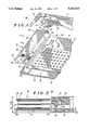
- This housingincludes a frame, a first cover, a carrier, a connector further including a body and a plurality of terminals, in addition to a second cover.
- the first coveris coupled to the frame and has an interior surface that is substantially planer plus an interface surface that is disposed parallel to the interior surface and spaced at an offset dimension that conforms to the type II PCMCIA standard.
- the carrierfor example a printed circuit board, is arranged to secure and inter couple an electronic circuit and has a first side that is disposed adjacent to the interior surface and a second side that is substantially uniformly spaced from the first side by a thickness dimension.
- the body of the connectorfurther includes a locating arm preferably including a raised element or the like, such as a protuberance, that establishes a physical relationship between the connector and the carrier, more specifically a mating element of the carrier.
- the frameincludes an interlocking feature for mechanically coupling the connector to the frame.
- the interlocking featureis preferably a slot and the body of the connector further includes a tab corresponding to the slot where the tab and the slot are cooperatively arranged so that the connector may be rotatably coupled to the frame. Providing a chamfer on the entry portion of the slot establishes a lead in surface for the tab when the connector is rotatably coupled to the frame.
- the frame (101)includes an interlocking feature (151) that, preferably, takes the form of one or more slots molded into each side rail (150, 152). As further discussed below the slots have a chamfer (153) that provides a lead in surface for rotatably coupling the connector to the frame (101).
- the coversspecifically the first or lower and second or upper covers (103, 137) are each, after assembly, substantially disposed in a plane, respectively, on a lower and a upper side of the frame (101) so that the second cover is spaced at a height dimension (239) from the first cover where the height dimension conforms to the PCMCIA standard which is a maximum of 5 millimeters (mm) for the type II PCMCIA standard.
- the covers (103, 137)are each formed from a blank sheet of metallic material, such as full hard aluminum, stainless steel, or the like and are fashioned to be physically or mechanically coupled to the frame (101) and to each other by means of an interlocking tab (158) arrangement disposed near and along the periphery of the covers and frame.
- the connector (121)includes a body (123), preferably, formed from molded plastic and a plurality of terminals (131) each of which is formed from a resilient and conductive material such as Phosphorus Bronze that is tin plated at the contact area and gold plated at the receptacle side.
- the connector (121)is, preferably, a 68 pin connector where the pins or terminals are arranged in a bottom or first and a top or second row such that all external dimensions and characteristics are compatible with the PCMCIA standard.
- the bodyis disposed adjacent to the interface surface (107) when assembled and further includes a first or front surface (125), a second or rear surface (127), and a plurality of openings (129).
- the body of the connectorincludes a tab (155), preferably one each proximate to the side rails of the frame corresponding to the interlocking feature (147), specifically the slot (151), that is cooperatively arranged so that the connector may be rotatably mechanically or physically coupled to the frame.
- the chamfer (153)provides a lead-in surface for the tab (155) as the connector is rotated into position and thus coupled to the frame.
- the tab (155) and the slot (151)provide a slight interference fit, during rotation, thus snapping into an assembled position that resists modest attempts to disassemble.
- the tabs (155)include a captive ledge (158) that laterally couples the frame (101) to the connector (121).
- the locating arm(s) (141)are captured between the carrier (111) and an undercut (156) in the cross web (154).
Landscapes
- Engineering & Computer Science (AREA)
- Microelectronics & Electronic Packaging (AREA)
- Connector Housings Or Holding Contact Members (AREA)
Abstract
Description
Claims (13)
Priority Applications (1)
| Application Number | Priority Date | Filing Date | Title |
|---|---|---|---|
| US08/270,354US5463531A (en) | 1994-07-05 | 1994-07-05 | PCMCIA electronics housing |
Applications Claiming Priority (1)
| Application Number | Priority Date | Filing Date | Title |
|---|---|---|---|
| US08/270,354US5463531A (en) | 1994-07-05 | 1994-07-05 | PCMCIA electronics housing |
Publications (1)
| Publication Number | Publication Date |
|---|---|
| US5463531Atrue US5463531A (en) | 1995-10-31 |
Family
ID=23030994
Family Applications (1)
| Application Number | Title | Priority Date | Filing Date |
|---|---|---|---|
| US08/270,354Expired - LifetimeUS5463531A (en) | 1994-07-05 | 1994-07-05 | PCMCIA electronics housing |
Country Status (1)
| Country | Link |
|---|---|
| US (1) | US5463531A (en) |
Cited By (15)
| Publication number | Priority date | Publication date | Assignee | Title |
|---|---|---|---|---|
| US5617627A (en)* | 1994-07-21 | 1997-04-08 | A.K. Stamping Co. Inc. | Method for making personal computer cards |
| US5754404A (en)* | 1996-05-14 | 1998-05-19 | Itt Cannon Gmbh | IC card rear board-connector support |
| US5764517A (en)* | 1996-04-22 | 1998-06-09 | International Business Machines Corporation | Computer cartridges assembly process line with integrated closure, weld, and marking stations |
| US5861602A (en)* | 1995-07-24 | 1999-01-19 | International Business Machines Corporation | Snap together PCMCIA cards with laser tack welded seams |
| WO1999014824A1 (en)* | 1997-09-15 | 1999-03-25 | Berg Technology, Inc. | Modem i/o connector |
| US5892660A (en)* | 1996-08-29 | 1999-04-06 | Micron Technology, Inc. | Single in line memory module adapter |
| US5894167A (en)* | 1996-05-08 | 1999-04-13 | Micron Technology, Inc. | Encapsulant dam standoff for shell-enclosed die assemblies |
| US5906516A (en)* | 1995-12-28 | 1999-05-25 | Yamaichi Electronics Co., Ltd. | Card-in type connector |
| US6071139A (en)* | 1998-03-31 | 2000-06-06 | Micron Technology, Inc. | Locking assembly for securing semiconductor device to carrier substrate |
| US6324076B1 (en) | 1997-05-22 | 2001-11-27 | Fci Americas Technology, Inc. | Electronic card with shield cover having tabs where each tab engages with recess of corresponding shield cover |
| US6370028B1 (en) | 1999-11-15 | 2002-04-09 | Itt Manufacturing Enterprises, Inc. | PC card with anti-smile cover |
| US20020053599A1 (en)* | 1996-11-08 | 2002-05-09 | Gerrits Antonius H.J. | Electronic card assembly and shell therefor |
| US6398573B1 (en) | 1998-03-31 | 2002-06-04 | Micron Technology, Inc. | Locking assembly for securing semiconductor device to carrier substrate |
| EP1073011A4 (en)* | 1998-04-14 | 2003-04-09 | Japan Solderless Terminal Mfg | Frame kit for pc card, pc card, and method of manufacturing pc card |
| US20040008502A1 (en)* | 2000-07-19 | 2004-01-15 | Frederic Hautier | Pack provided with an antenna extension for electronic card and method for the assembling of the pack |
Citations (3)
| Publication number | Priority date | Publication date | Assignee | Title |
|---|---|---|---|---|
| US5339222A (en)* | 1993-04-06 | 1994-08-16 | The Whitaker Corporation | Shielded printed circuit card holder |
| US5373149A (en)* | 1993-02-01 | 1994-12-13 | At&T Bell Laboratories | Folding electronic card assembly |
| US5408386A (en)* | 1992-10-30 | 1995-04-18 | Intel Corporation | Socket assembly including a first circuit board located between a receptacle housing and a second circuit board |
- 1994
- 1994-07-05USUS08/270,354patent/US5463531A/ennot_activeExpired - Lifetime
Patent Citations (3)
| Publication number | Priority date | Publication date | Assignee | Title |
|---|---|---|---|---|
| US5408386A (en)* | 1992-10-30 | 1995-04-18 | Intel Corporation | Socket assembly including a first circuit board located between a receptacle housing and a second circuit board |
| US5373149A (en)* | 1993-02-01 | 1994-12-13 | At&T Bell Laboratories | Folding electronic card assembly |
| US5339222A (en)* | 1993-04-06 | 1994-08-16 | The Whitaker Corporation | Shielded printed circuit card holder |
Cited By (32)
| Publication number | Priority date | Publication date | Assignee | Title |
|---|---|---|---|---|
| US5617627A (en)* | 1994-07-21 | 1997-04-08 | A.K. Stamping Co. Inc. | Method for making personal computer cards |
| US6108209A (en)* | 1995-07-24 | 2000-08-22 | International Business Machines Corporation | Snap together PCMCIA cards with laser tack welded seams |
| US5861602A (en)* | 1995-07-24 | 1999-01-19 | International Business Machines Corporation | Snap together PCMCIA cards with laser tack welded seams |
| US6194683B1 (en) | 1995-07-24 | 2001-02-27 | International Business Machines Corporation | Snap together PCMCIA cards with laser tack welded seams |
| US5906516A (en)* | 1995-12-28 | 1999-05-25 | Yamaichi Electronics Co., Ltd. | Card-in type connector |
| US5764517A (en)* | 1996-04-22 | 1998-06-09 | International Business Machines Corporation | Computer cartridges assembly process line with integrated closure, weld, and marking stations |
| US5894167A (en)* | 1996-05-08 | 1999-04-13 | Micron Technology, Inc. | Encapsulant dam standoff for shell-enclosed die assemblies |
| US5895222A (en)* | 1996-05-08 | 1999-04-20 | Micron Technology, Inc. | Encapsulant dam standoff for shell-enclosed die assemblies |
| US5754404A (en)* | 1996-05-14 | 1998-05-19 | Itt Cannon Gmbh | IC card rear board-connector support |
| US6570771B2 (en) | 1996-08-29 | 2003-05-27 | Micron Technology, Inc. | Single-piece molded module housing |
| US5892660A (en)* | 1996-08-29 | 1999-04-06 | Micron Technology, Inc. | Single in line memory module adapter |
| US6233154B1 (en) | 1996-08-29 | 2001-05-15 | Micron Technology, Inc. | Single-piece molded module housing |
| US6781848B2 (en) | 1996-08-29 | 2004-08-24 | Micron Technology, Inc. | Single-piece molded module housing |
| US20030193788A1 (en)* | 1996-08-29 | 2003-10-16 | Farnworth Warren M. | Single-piece molded module housing |
| US20020053599A1 (en)* | 1996-11-08 | 2002-05-09 | Gerrits Antonius H.J. | Electronic card assembly and shell therefor |
| US6905073B2 (en) | 1996-11-08 | 2005-06-14 | Fci Americas Technology, Inc. | Electronic card assembly and shell therefor |
| US6533177B1 (en)* | 1996-11-08 | 2003-03-18 | Fci Americas Technology, Inc. | Electronic card assembly and shell therefor |
| US6324076B1 (en) | 1997-05-22 | 2001-11-27 | Fci Americas Technology, Inc. | Electronic card with shield cover having tabs where each tab engages with recess of corresponding shield cover |
| WO1999014824A1 (en)* | 1997-09-15 | 1999-03-25 | Berg Technology, Inc. | Modem i/o connector |
| US6368136B2 (en) | 1998-03-31 | 2002-04-09 | Micron Technology, Inc. | Locking assembly for securing semiconductor device to carrier substrate |
| US6457985B1 (en) | 1998-03-31 | 2002-10-01 | Micron Technology, Inc. | Locking assembly for securing semiconductor device to carrier substrate |
| US6565374B2 (en) | 1998-03-31 | 2003-05-20 | Micron Technology, Inc. | Locking assembly for securing semiconductor device to carrier substrate |
| US6398573B1 (en) | 1998-03-31 | 2002-06-04 | Micron Technology, Inc. | Locking assembly for securing semiconductor device to carrier substrate |
| US6071139A (en)* | 1998-03-31 | 2000-06-06 | Micron Technology, Inc. | Locking assembly for securing semiconductor device to carrier substrate |
| US6648663B2 (en) | 1998-03-31 | 2003-11-18 | Micron Technology, Inc. | Locking assembly for securing semiconductor device to carrier substrate |
| US6302719B1 (en) | 1998-03-31 | 2001-10-16 | Micron Technology, Inc. | Locking assembly for securing semiconductor device to carrier substrate |
| US6837731B2 (en) | 1998-03-31 | 2005-01-04 | Micron Technology, Inc. | Locking assembly for securing a semiconductor device to a carrier substrate |
| US6238228B1 (en) | 1998-03-31 | 2001-05-29 | Micron Technology, Inc. | Locking assembly for securing semiconductor device to carrier substrate |
| EP1073011A4 (en)* | 1998-04-14 | 2003-04-09 | Japan Solderless Terminal Mfg | Frame kit for pc card, pc card, and method of manufacturing pc card |
| US6370028B1 (en) | 1999-11-15 | 2002-04-09 | Itt Manufacturing Enterprises, Inc. | PC card with anti-smile cover |
| US20040008502A1 (en)* | 2000-07-19 | 2004-01-15 | Frederic Hautier | Pack provided with an antenna extension for electronic card and method for the assembling of the pack |
| US6769621B2 (en)* | 2000-07-19 | 2004-08-03 | Fci | Pack provided with an antenna extension for electronic card and method for the assembling of the pack |
Similar Documents
| Publication | Publication Date | Title |
|---|---|---|
| US5463531A (en) | PCMCIA electronics housing | |
| KR100208639B1 (en) | Universal grounding clip for card-receiving connector | |
| US7435139B2 (en) | Electrical connector having improved shield | |
| US7422482B2 (en) | Electrical connector having improved shield | |
| US6074223A (en) | Compact flash card having a grounding tab | |
| US7497733B1 (en) | Shielded connector adapted to be mounted at different profile | |
| KR0161558B1 (en) | Memory card and how to assemble it | |
| US20060234530A1 (en) | Electrical connector with retaining device | |
| US5749741A (en) | Electrical connector with ground clip | |
| JPH0668319A (en) | Data card, whose periphery is shielded | |
| US20060189216A1 (en) | Camera module connector keying structure | |
| US6099353A (en) | IC card connector | |
| US6626689B1 (en) | Electrical card connector | |
| US20080166921A1 (en) | Shielded connector | |
| US20040248443A1 (en) | Electrical card connector having shutter mechanism | |
| US7442082B2 (en) | Shielded connector with folding arrangement ensuring perpendicularity between sidewall and bottom wall of the metal housing | |
| US7559799B2 (en) | Electrical connector | |
| US6129588A (en) | Smart card connector having openings for exposing signal terminals of the connector and accommodating other electronic elements | |
| US6469912B1 (en) | Electrical apparatus having a cover member adapted to provide electromagnetic interference shielding to an electronic component | |
| US6116920A (en) | Alignment socket for PCMCIA card connector | |
| US6319017B1 (en) | Electrical card connector | |
| CA2174130C (en) | Ic card with board positioning means | |
| US6722921B1 (en) | Electrical card connector | |
| US6736656B1 (en) | Electrical card connector | |
| US6068510A (en) | Electrical card connector |
Legal Events
| Date | Code | Title | Description |
|---|---|---|---|
| AS | Assignment | Owner name:MOTOROLA, INC., ILLINOIS Free format text:ASSIGNMENT OF ASSIGNORS INTEREST;ASSIGNORS:CHOON, LOW POH;REDMAN, BRIAN L.;REEL/FRAME:007191/0289 Effective date:19940901 | |
| STCF | Information on status: patent grant | Free format text:PATENTED CASE | |
| FPAY | Fee payment | Year of fee payment:4 | |
| FPAY | Fee payment | Year of fee payment:8 | |
| REMI | Maintenance fee reminder mailed | ||
| FPAY | Fee payment | Year of fee payment:12 | |
| AS | Assignment | Owner name:MOTOROLA MOBILITY, INC, ILLINOIS Free format text:ASSIGNMENT OF ASSIGNORS INTEREST;ASSIGNOR:MOTOROLA, INC;REEL/FRAME:025673/0558 Effective date:20100731 | |
| AS | Assignment | Owner name:MOTOROLA MOBILITY LLC, ILLINOIS Free format text:CHANGE OF NAME;ASSIGNOR:MOTOROLA MOBILITY, INC.;REEL/FRAME:029216/0282 Effective date:20120622 | |
| AS | Assignment | Owner name:GOOGLE TECHNOLOGY HOLDINGS LLC, CALIFORNIA Free format text:ASSIGNMENT OF ASSIGNORS INTEREST;ASSIGNOR:MOTOROLA MOBILITY LLC;REEL/FRAME:034474/0001 Effective date:20141028 |