US5462467A - Fabrication of filamentary field-emission device, including self-aligned gate - Google Patents
Fabrication of filamentary field-emission device, including self-aligned gateDownload PDFInfo
- Publication number
- US5462467A US5462467AUS08/118,490US11849093AUS5462467AUS 5462467 AUS5462467 AUS 5462467AUS 11849093 AUS11849093 AUS 11849093AUS 5462467 AUS5462467 AUS 5462467A
- Authority
- US
- United States
- Prior art keywords
- layer
- filaments
- conductive region
- pores
- gate
- Prior art date
- Legal status (The legal status is an assumption and is not a legal conclusion. Google has not performed a legal analysis and makes no representation as to the accuracy of the status listed.)
- Expired - Lifetime
Links
Images


Classifications
- H—ELECTRICITY
- H01—ELECTRIC ELEMENTS
- H01J—ELECTRIC DISCHARGE TUBES OR DISCHARGE LAMPS
- H01J1/00—Details of electrodes, of magnetic control means, of screens, or of the mounting or spacing thereof, common to two or more basic types of discharge tubes or lamps
- H01J1/02—Main electrodes
- H01J1/30—Cold cathodes, e.g. field-emissive cathode
- H01J1/304—Field-emissive cathodes
- H01J1/3042—Field-emissive cathodes microengineered, e.g. Spindt-type
- B—PERFORMING OPERATIONS; TRANSPORTING
- B82—NANOTECHNOLOGY
- B82Y—SPECIFIC USES OR APPLICATIONS OF NANOSTRUCTURES; MEASUREMENT OR ANALYSIS OF NANOSTRUCTURES; MANUFACTURE OR TREATMENT OF NANOSTRUCTURES
- B82Y10/00—Nanotechnology for information processing, storage or transmission, e.g. quantum computing or single electron logic
- H—ELECTRICITY
- H01—ELECTRIC ELEMENTS
- H01J—ELECTRIC DISCHARGE TUBES OR DISCHARGE LAMPS
- H01J3/00—Details of electron-optical or ion-optical arrangements or of ion traps common to two or more basic types of discharge tubes or lamps
- H01J3/02—Electron guns
- H01J3/021—Electron guns using a field emission, photo emission, or secondary emission electron source
- H01J3/022—Electron guns using a field emission, photo emission, or secondary emission electron source with microengineered cathode, e.g. Spindt-type
- H—ELECTRICITY
- H01—ELECTRIC ELEMENTS
- H01J—ELECTRIC DISCHARGE TUBES OR DISCHARGE LAMPS
- H01J9/00—Apparatus or processes specially adapted for the manufacture, installation, removal, maintenance of electric discharge tubes, discharge lamps, or parts thereof; Recovery of material from discharge tubes or lamps
- H01J9/02—Manufacture of electrodes or electrode systems
- H01J9/022—Manufacture of electrodes or electrode systems of cold cathodes
- H01J9/025—Manufacture of electrodes or electrode systems of cold cathodes of field emission cathodes
- H—ELECTRICITY
- H01—ELECTRIC ELEMENTS
- H01J—ELECTRIC DISCHARGE TUBES OR DISCHARGE LAMPS
- H01J2201/00—Electrodes common to discharge tubes
- H01J2201/30—Cold cathodes
- H01J2201/304—Field emission cathodes
- H01J2201/30403—Field emission cathodes characterised by the emitter shape
- H—ELECTRICITY
- H01—ELECTRIC ELEMENTS
- H01J—ELECTRIC DISCHARGE TUBES OR DISCHARGE LAMPS
- H01J2201/00—Electrodes common to discharge tubes
- H01J2201/30—Cold cathodes
- H01J2201/304—Field emission cathodes
- H01J2201/30446—Field emission cathodes characterised by the emitter material
- H01J2201/30453—Carbon types
- H01J2201/30457—Diamond
- H—ELECTRICITY
- H01—ELECTRIC ELEMENTS
- H01J—ELECTRIC DISCHARGE TUBES OR DISCHARGE LAMPS
- H01J2201/00—Electrodes common to discharge tubes
- H01J2201/30—Cold cathodes
- H01J2201/319—Circuit elements associated with the emitters by direct integration
- Y—GENERAL TAGGING OF NEW TECHNOLOGICAL DEVELOPMENTS; GENERAL TAGGING OF CROSS-SECTIONAL TECHNOLOGIES SPANNING OVER SEVERAL SECTIONS OF THE IPC; TECHNICAL SUBJECTS COVERED BY FORMER USPC CROSS-REFERENCE ART COLLECTIONS [XRACs] AND DIGESTS
- Y10—TECHNICAL SUBJECTS COVERED BY FORMER USPC
- Y10T—TECHNICAL SUBJECTS COVERED BY FORMER US CLASSIFICATION
- Y10T428/00—Stock material or miscellaneous articles
- Y10T428/29—Coated or structually defined flake, particle, cell, strand, strand portion, rod, filament, macroscopic fiber or mass thereof
- Y10T428/2913—Rod, strand, filament or fiber
- Y10T428/2973—Particular cross section
- Y—GENERAL TAGGING OF NEW TECHNOLOGICAL DEVELOPMENTS; GENERAL TAGGING OF CROSS-SECTIONAL TECHNOLOGIES SPANNING OVER SEVERAL SECTIONS OF THE IPC; TECHNICAL SUBJECTS COVERED BY FORMER USPC CROSS-REFERENCE ART COLLECTIONS [XRACs] AND DIGESTS
- Y10—TECHNICAL SUBJECTS COVERED BY FORMER USPC
- Y10T—TECHNICAL SUBJECTS COVERED BY FORMER US CLASSIFICATION
- Y10T428/00—Stock material or miscellaneous articles
- Y10T428/29—Coated or structually defined flake, particle, cell, strand, strand portion, rod, filament, macroscopic fiber or mass thereof
- Y10T428/2913—Rod, strand, filament or fiber
- Y10T428/298—Physical dimension
Definitions
- This inventionrelates to electron-emitting devices. More particularly, this invention relates to structures and manufacturing techniques for field-emission devices (or field emitters) suitable for products such as cathode-ray tubes of the flat-panel type.
- a field-emission cathodeis an electronic device that emits electrons when subjected to an electric field of sufficient strength.
- the electric fieldis created by applying a voltage between the cathode and an electrode, typically referred to as the anode or gate electrode, situated a short distance away from the cathode.
- Field emittersare employed in cathode-ray tubes of flat-panel televisions.
- Yoshida et alU.S. Pat. No. 5,164,632 discloses a field-emission structure in which solid elongated gold electron-emissive elements are situated in pores extending through an alumina (aluminum oxide) layer. An address line lying under the alumina layer contacts the lower ends of the electron-emissive elements. Their upper ends are pointed. A gate electrode situated above the electron-emissive elements extends slightly into the pores.
- Yoshida et alanodically oxidize part of an aluminum plate to create a thin alumina layer having pores that extend nearly all the way through the alumina.
- An electrolytic techniqueis used to fill the pores with gold for the electron-emissive elements.
- the address lineis formed over the filled pores along the alumina side of the structure after which the remaining aluminum and part of the adjoining alumina are removed along the opposite side of the structure to re-expose the gold in the pores.
- Part of the re-exposed goldis removed during an ion-milling process utilized to sharpen the electron-emissive elements.
- Goldis then evaporatively deposited onto the alumina and partly into the pores to form the gate electrode.
- Greene et alU.S. Pat. No. 5,150,192, discloses a field emitter in which hollow elongated electron-emissive elements extend through a thin electrically insulating substrate.
- the electron-emissive elementshave pointed tips that protrude into cavities provided along the upper substrate surface below a gate electrode.
- a metal filmlies along the lower substrate surface.
- Greene et alcreate openings partway through the substrate by etching through a mask formed on the bottom of the substrate. Metal is deposited along the walls of the openings and along the lower substrate surface. A portion of the thickness of the substrate is removed along the upper surface. The gate electrode is then formed by a deposition/planarization procedure. The cavities are provided along the upper substrate surface after which the hollow metal portions in the openings are sharpened to complete the electron-emissive elements.
- a large-area field emitter for an application such as a flat-panel television screen where the diagonal screen dimension is 25 cmneeds a relatively strong substrate for supporting the field-emission components extending across the large emitter area.
- the requisite substrate thicknessis typically several hundred microns to 10 mm or more. Due to the ways in which Yoshida et al and Greene et al manufacture their field emitters, it would be quite difficult to attach those emitters to substrates of such thickness. Consequently, Yoshida et al and Greene et al are not suited for scaling up to large-area field-emission applications.
- Busta"Vacuum Microelectronics-1992,” J. Micromech. Microeng., Vol. 2, 1992, pp. 43-74, provides a general review of field-emission devices. Among other things, Busta discusses Utsumi, “Keynote Address, Vacuum Microelectronics: What's New and Exciting,” IEEE Trans Elect. Dev., Oct. 1990, pp. 2276-2283, who suggests that a filament with a rounded end is the best shape for a field-emission element. Busta also discusses Betsui, "Fabrication and Characteristics of Si Field Emitter Arrays," Tech. Dig. IVMC 91, 1991, pp.
- the present inventionfurnishes an efficient, reliable field-emission structure fabricated according to a simple, accurate, and easily controllable process.
- the inventionutilizes electrically conductive filaments as electron-emissive elements. Each filament is an elongated solid body whose length is considerably greater than its maximum transverse dimension. A self-aligned gate electrode is typically employed with the filaments.
- a lower electrically conductive regionis situated over electrically insulating material of a substrate that provides support for the structure, especially when the lower conductive region includes a group of generally parallel lines.
- a porous electrically insulating layerlies over the lower conductive region.
- a multiplicity of electron-emissive filamentsoccupy corresponding pores extending through the porous layer. The lower end of each filament contacts the lower conductive region.
- the gate electrodeWhen a gate electrode is incorporated into the field emitter, the gate electrode is implemented with a patterned electrically conductive gate layer that lies over the porous insulating layer. Openings extend through the gate layer at locations centered on the filaments in such a manner that the filaments are separated from the gate layer. Cavities are normally provided in the porous layer along its upper surface at locations likewise centered on the filaments. The cavities extend partway through the porous layer. Each cavity is wider than the corresponding pore so that each filament protrudes from its pore into the corresponding cavity.
- the porous layeris formed over the lower conductive region with pores extending fully through the porous layer.
- the poresare preferably created by etching charged-particle tracks formed through an electrically insulating layer situated over the lower conductive region. As a result, the pores are distributed at random locations relative to one another.
- Electrically conductive filament materialis subsequently introduced into the pores to form the electron-emissive filaments. This step is preferably done by electrochemically depositing the filament material into the pores starting from the lower conductive region. Due to the selective nature of the electrochemical deposition, filaments are created only in pores lying over the lower conductive region.
- the gate layeris subsequently provided over the porous layer in a self-aligned manner.
- Two proceduresare available for creating the gate layer in this way.
- electrically conductive capsare provided over the upper ends of the filaments.
- Each capis formed over a corresponding one of the filaments and has a lateral periphery that encloses the lateral periphery of the corresponding filament along the bottom of the cap.
- An electrochemical deposition techniqueis preferably utilized to create the caps in this manner so that they are self-aligned to the filaments.
- One of the proceduresinvolves removing part of the thickness of the porous layer. Electrically conductive gate material is deposited over the remainder of the porous layer into the space generally below the space between the caps.
- the capsshield the underlying portions of the porous layer so as to substantially prevent the gate material from accumulating on the portions of the porous layer located below the caps. Some of the gate material invariably accumulates on the caps during the deposition. The caps are then lifted off along with any of the gate material on the caps. The remainder of the gate material forms the patterned gate layer.
- the gate layeris formed in the space between the caps. This entails depositing a blanket layer of the gate material over the porous layer and the caps, after which the gate material over the caps is removed, preferably by a planarization technique. The caps are then removed. The remainder of the gate material again forms the gate layer.
- the pattern of openings through the gate layeris defined before the pores are created through the insulating layer. More specifically, the gate layer is first provided over the insulating layer. At this point, the gate layer does not have the openings, and the insulating layer does not have the pores.
- the openingsare now formed through the gate layer to expose corresponding surface portions of the insulating layer.
- Thistypically involves providing a further layer over the gate layer.
- Charged particlesare passed through the three layers to form charged-particle tracks down to the lower conductive region.
- Each trackhas two segments: (a) a first segment extending through the insulating layer and (b) a second segment extending through the further layer in line with the first segment.
- the further layeris etched along the second track segments to form corresponding apertures through the further layer.
- the gate layeris subsequently etched through the apertures to form the openings.
- Each opening through the gate layeris thereby centered on a corresponding one of the apertures through the further layer.
- each poreis formed through part, but not all, of the exposed surface portion of the corresponding gate-layer opening in such a way that each pore is generally centered on the corresponding gate-layer opening but is considerably narrower than that opening along the bottom of the gate layer.
- the poresare created in a self-aligned manner by etching the insulating layer along the first track segments down to the gate layer.
- the filament materialis now introduced into the pores to define the filaments.
- the cavitiesare created around the filaments by removing material of the porous insulating layer exposed through the openings in the gate layer.
- the upper ends of the filamentsare preferably sharpened.
- the edges of the gate layercan also be rounded to complete the field-emitter fabrication.
- charged-particle tracks and electrochemical processingare employed in a judicious manner to create the electron-emissive filaments at selected locations and to self-align the gate layer to the filaments.
- No conventional lithographic patterning stepsare needed for these two fabrication activities.
- the components of the field-emission structurecan be manufactured at lateral dimensions on the nanometer scale.
- the fabrication process of the inventionis simple and highly accurate.
- the processis inexpensive and well-suited for scaling up to manufacturing large-area field emitters for cathode-ray tubes in flat-panel televisions.
- the inventionprovides a substantial advance over the prior art.
- FIGS. 1a, 1b, 1c, 1d, and 1eare cross-sectional front structural views representing steps in fabricating a field-emission structure according to the invention.
- FIGS. 2a, 2b, 2c, 2d, and 2eare plan views respectively corresponding to FIGS. 1a-1e.
- the cross sections of FIGS. 1a-1eare taken through stepped plane 1--1 in FIGS. 2a-2e.
- FIGS. 3a and 3bare cross-sectional front structural views representing a set of additional fabrication steps performable on the structure of FIGS. 1e and 2e according to the invention.
- FIGS. 4a and 4bare cross-sectional side structural views respectively corresponding to FIGS. 3a and 3b.
- the cross sections of FIGS. 3a and 3bare taken through plane 3--3 in FIGS. 4a and 4b.
- the cross sections of FIGS. 4a and 4bare similarly taken through plane 4--4 in FIGS. 3a and 3b.
- FIGS. 5a and 5bare cross-sectional front structural views representing another set of additional fabrication steps performable on the structure of FIGS. 1e and 2e according to the invention.
- FIGS. 6a and 6bare cross-sectional side structural views respectively corresponding to FIGS. 5a and 5b.
- the cross sections of FIGS. 6a and 6bare similarly taken through plane 6--6 in FIGS. 5a and 5b.
- FIGS. 7a, 7b, 7c, 7d, 7e, and 7fare cross-sectional front structural views representing a set of fabrication steps for adding a gate electrode to the structure of FIGS. 1e and 2e according to the invention.
- FIGS. 8a, 8b, 8c, 8d, 8e, and 8fare plan views respectively corresponding to FIGS. 7a-7f.
- the cross sections of FIGS. 7a-7fare taken through stepped plane 7--7 in FIGS. 8a-8f.
- FIGS. 9a, 9b, 9c, 9d, 9e, and 9fare cross-sectional front structural views representing another set of fabrication steps for adding a gate electrode to the structure of FIGS. 1e and 2e according to the invention.
- FIGS. 10a, 10b, 10c, 10d, 10e, and 10fare plan views respectively corresponding to FIGS. 9a-9f.
- the cross sections of FIGS. 9a-9fare taken through stepped plane 9--9 in FIGS. 10a-10f.
- FIGS. 11a, 11b, 11c, 11d, 11e, 11f, 11g, 11h, 11i, and 11jare cross-sectional front structural views representing steps in fabricating a gated field-emission structure according to the invention.
- FIGS. 12a, 12b, 12c, 12d, 12e, 12f, 12g, 12h, 12i, and 12jare plan views respectively corresponding to FIGS. 11a-11j.
- the cross sections of FIGS. 11a-11jare taken through stepped plane 11--11 in FIGS. 12a-12j.
- FIGS. 13a and 13bare cross-sectional front structural views representing steps that can be substituted for the steps shown in FIGS. 11d and 11e.
- FIG. 14is a cross-sectional front structural view depicting how the initial structures of FIGS. 1a and 11a appear when the lower conductive region consists of a highly conductive portion and a highly resistive portion.
- FIG. 15is a cross-sectional side structural view corresponding to FIG. 14.
- the cross section of FIG. 14is taken through plane 14--14 in FIG. 15.
- the cross section of FIG. 15is taken through plane 15--15 in FIG. 14.
- FIGS. 16.1 and 16.2are cross-sectional front structural views respectively depicting how the final structures of FIGS. 3b and 11j appear when they contain the two-part lower conductive region of FIG. 14.
- FIG. 17a, 17b, 17c, 17d, 17e, 17f, 17g, 17h, 17i, 17j, 17k, and 17lare cross-sectional front structural views representing steps in manufacturing a gated field-emission structure that incorporates a focusing electrode according to the invention.
- FIGS. 18.1, 18.2, 18.3 and 18.4are cross-sectional longitudinal views of differently shaped electron-emissive filaments usable in the field-emission structures of the invention.
- FIG. 19is a functional diagram for the components of an electrochemical deposition system used in the invention.
- the present inventionmakes extensive use of electrochemical deposition in which a material, usually a metal, is deposited from an (ionized) electrolyte in a (liquid) solvent. Electrochemical deposition is typically performed by passing current between a pair of electrodes to enable the material to accumulate on one of the electrodes. Nonetheless, electrochemical deposition can be performed in an electroless manner at zero applied potential.
- FIGS. 1a-1e and 2a-2eillustrate a process for manufacturing a field-emission cathode structure according to the teachings of the invention.
- the field-emission structureis typically used to excite phosphors on a face plate in a cathode-ray tube of a flat-panel television screen.
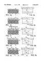
- the starting point for the fabrication processis an electrically insulating substrate 20 consisting of ceramic or glass.
- Substrate 20is typically configured as a plate having a largely flat upper surface and a largely flat lower surface substantially parallel to the upper surface.
- Substrate 20furnishes support for the field-emission structure.
- the substrate thicknessis at least 500 microns.
- the substrate thicknessis typically 4-14 mm. If support struts are placed between the phosphor-coated face plate and the field emitter, the substrate thickness is typically 1-2 mm.
- a lower electrically conductive region 22is formed along the top of substrate 20 as indicated in FIGS. 1a and 2a.
- Lower conductive region 22consists of a metal such as chromium. In this case, the thickness of region 22 is 0.05-1.5 micron.
- Other candidates for region 22include tantalum, tungsten, and molybdenum.
- Lower conductive region 22is typically a patterned layer containing a group of parallel lines, of which two such lines are depicted in FIG. 2a.
- region 22is configured in this way, the final field-emission structure is particularly suitable for selectively exciting phosphors in a flat-panel television.
- These linesare typically 300 microns wide for the 25-cm monochrome flat-panel television example. Nonetheless, region 22 can be arranged in various other patterns, or can even be unpatterned.
- a largely homogeneous electrically insulating layer 24is formed on the top of the structure. See FIGS. 1b and 2b. Parts of insulating layer 24 are situated on both substrate 20 and lower conductive region 22. The thickness of layer 24 is 0.1-2.0 microns, typically 0.5 micron. Suitable materials for insulating layer 24 fall into three groups: (a) organic polymers such as polycarbonate, polystyrene, and cellulose acetate, (b) inorganic glasses such as phosphate, and soda-lime glasses, and (c) crystals such as mica and quartz.
- Insulating layer 24is subjected to energetic charged particles that impinge on the top of layer 24 in a direction largely perpendicular to the lower surface of substrate 20 and thus in a direction generally perpendicular to the upper structural surface.
- the charged particleshave sufficient energy to form straight tracks through layer 24 at random locations across layer 24.
- the charged-particle tracksconstitute damaged zones created along the paths of the charged particles. As shown in FIGS. 1c and 2c, the tracks consist of (a) charged-particle tracks 26 1 through the portions of layer 24 overlying conductive region 22 and (b) charged-particle 26 2 through the portions of layer 24 directly overlying substrate 20.
- Charged-particle tracks 26 1 and 26 2extend parallel to one another in a direction generally perpendicular to the upper structural surface. Although charged-particle tracks 26 are randomly distributed across insulating layer 24, they have a well-defined average spacing. The track density can be as much as 10 11 tracks/cm 2 . A typical value is 10 7 tracks/cm 2 which yields an average track spacing of approximately 3 microns. For illustrative purposes, only a very small portion of tracks 26 are indicated in FIGS. 1c and 2c.
- the charged particlespenetrate into the material below insulator 24. Such penetration is not material here and, accordingly, is not shown in the drawings.
- a charged-particle acceleratorwhich forms a well-collimated beam of ions is employed to form tracks 26.
- the ion beamis scanned uniformly across insulating layer 24.
- the preferred charged-particle speciesis doubly ionized argon (Ar ++ ) at an energy of 8 MeV.
- tracks 26could be created from a collimated source of nuclear fission particles produced, for example, by the radioactive element californium 252.
- Insulating layer 24is brought into contact with (e.g., by immersion) a suitable chemical etchant that attacks the damaged insulating material along tracks 26 much more than the undamaged material of layer 24. Pores 28 1 and 28 2 are thereby etched through layer 24 respectively along tracks 26 1 and 26 2 . See FIGS. 1d and 2d. For illustrative purposes, the lateral dimensions of pores 28 1 and 28 2 (collectively "28") compared to the widths of the lines that form conductive layer 20 are greatly exaggerated in the plan-view drawings. The remainder of insulating layer 24 now constitutes homogeneous porous insulating layer 24A.
- Pores 28are generally circular in shape as viewed from the top in the plan view of FIG. 2d. Depending on how the track etching is done, pores 28 can be cylindrical or (slightly) conical in three dimensions. For purposes of illustration, pores 28 are represented as cylinders in the drawings.
- the pore diametercan vary from 4 nm to 2 microns. Preferably, the pore diameter lies in the range of 10-200 nm. A typical value is 100 nm.
- the etchant used for creating pores 28preferably does not significantly attack substrate 20 or conductive region 22.
- components 20, 22, and 24Arespectively consist of ceramic, chromium, and polycarbonate
- the etchingis done in 6.25 normal sodium hydroxide at 50° C.
- the etch timeis 2-3 minutes for the typical 0.5-micron porous-layer thickness.
- Solid electron-emissive metal filaments 30are formed in pores 28 1 , which overlie conductive region 22, by electrochemically depositing a suitable filament metal. See FIGS. 1e and 2e.
- the depositionis performed in an electrochemical cell, described below, in which conductive region 22 acts as a deposition cathode. After bringing the structure into contact with the cell electrolyte and activating the cell, current flows between cathode 22 and a separate anode.
- the filament materialuniformly builds up in pores 28 1 starting from conductive region 22. The lower ends of filaments 30 contact region 22. Because pores 28 1 are situated randomly across porous layer 24, filaments 30 are likewise situated at random locations above conductive region 22.
- the electrochemical depositionis typically performed for a time sufficient to enable the upper ends of pores 30 to be nearly coplanar with top of porous layer 24A. This situation is illustrated in FIG. 1e.
- the depositioncan, however, be performed for a longer time so that filaments 30 bulge slightly out of pores 28 1 or for a shorter time so that the upper ends of filaments 30 are significantly below the top of layer 24A.
- the upper ends of filaments 30are preferably formed with a noble metal.
- the upper ends of filaments 30consist of platinum when conductive region 22 is chromium.
- Other candidate noble metals for the upper filament endsare gold and palladium.
- the remaining portions of filaments 30typically consist of the same (noble) metal as the upper ends but can be formed with another metal such as nickel, copper, or cobalt.
- Elements 30are true filaments for which the ratio of length to maximum diameter is at least 2 and normally at least 3.
- the length-to-maximum-diameter ratiois preferably 5 or more.
- Filaments 30are typically cylinders of circular transverse cross section. Nonetheless, the transverse cross section can be somewhat non-circular. In any case, the ratio of maximum diameter to minimum diameter for each filament 30 is usually no more than 2.
- Filaments 30are all of substantially the same length.
- the filament lengthis 0.1-2.0 microns, typically 0.5 micron.
- the average track spacing and, consequently, the average filament spacingare arranged to be somewhat greater than the filament length.
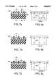
- FIGS. 3a, 3b, 4a, and 4bthey illustrate additional steps that can be performed on the structure of FIGS. 1e and 2e to accomplish these two objectives.
- the first additional stepis to uniformly remove part of the thickness of porous layer 24A with an etchant that does not significantly attack the filament metal.
- the etchantdoes not significantly attack substrate 20 or conductive region 22.
- FIGS. 3a and 4adepict the structure at the end of this etching step.
- Item 24Bis the reduced-thickness remainder of porous layer 24A.
- the upper ends of filaments 30are sharpened by performing an electropolishing and etching operation.
- the electropolishingwhich is done first, rounds the upper ends of filaments 30 and reduces their length somewhat.
- the etchsharpens the rounded filament ends.
- the electropolishingis performed in an electrolytic cell in which filaments 30 constitute the anode. After bringing the structure of FIGS. 3a and 4a into contact with the cell electrolyte, a suitable potential is applied between (a) filaments 30 by way of lower conductive region 22 and (b) a separate cathode plate to cause current to flow between filaments 30 and the cathode plate.
- the electropolishingis typically conducted in an operational regime where the rate of metal removal increases with increasing electric field strength. Because the highest electric field, and thus the greatest material removal rate, for each filament 30 occurs at the outer top filament edge, the upper ends of filaments 30 become rounded.
- the filament etchis also typically done by bringing the field-emission structure into contact with the electrolyte of an electrolytic cell in which filaments 30 constitute the anode to which a driving voltage is applied via lower conductive region 22.
- the rate of metal removalvaries with electric field strength and filament morphology in such a way that the rounded upper ends of filaments 30 become pointed.
- the etchcan also be done according to a chemical technique.
- FIGS. 3b and 4bdepict the final structure in which sharpened filaments 30A are the remainders of original filaments 30.
- FIGS. 5a, 5b, 6a, and 6bdepict how this alternative procedure is performed starting from the structure of FIGS. 1e and 2e.
- Porous layer 24Ais first removed as shown in FIGS. 5a and 6a.
- components 22, 24A, and 30respectively are chromium, polycarbonate, and platinum, the removal step is typically performed by dissolving layer 24A with dichloromethane.
- An electropolishing and etching operationis then performed to sharpen the upper ends of filaments 30 in the manner shown in FIGS. 5b and 6b. Items 30A are again the sharpened remainders of filaments 30.
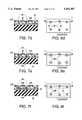
- FIGS. 7a-7f and 8a-8fillustrate a group of steps for providing the cathode structure of FIGS. 1e and 2e with a self-aligned gate-electrode structure.
- porous layer 24Apreferably consists of an inorganic glass.
- the initial thickness of layer 24Ais typically 0.8 micron.
- the first step in creating the gate electrodeis to electrochemically deposit electrically conductive caps 32 respectively on filaments 30. See FIGS. 7a and 8a. Caps 32 are generally circular in shape as viewed from the top in FIG. 8a.
- each cap 32is centered on the upper end of corresponding filament 30. Along the upper surface of porous layer 24A, each cap 32 also reaches a greater diameter than underlying filament 30. As a result, each cap 32 has a lateral periphery that encloses the lateral periphery of underlying filament 30 along the top of layer 24A. Typically, the average diameter of caps 30 along the top of layer 24A is at least 1.5 times the average diameter of filaments 30.
- the electrochemical deposition to create caps 32is performed in an electrochemical cell, again described below, in which filaments 30 (attached to lower conductive region 22) act as a cathode. After the structure has been brought into contact with the cell electrolyte and the cell has been activated, current flows between filaments 30 and a separate anode. The cap material thereby builds up on filaments 30 until the desired cap diameter is reached.
- Caps 32consist of a metal different from the filament metal along the upper ends of filament 30.
- the cap metalis selectively etchable with respect to the directly underlying filament metal.
- filaments 30consist of platinum
- caps 32are formed with a metal such as silver whose half-cell potential is less positive than that of platinum.
- porous layer 24Ais uniformly removed along the top of layer 24A to produce the structure shown in FIGS. 7b and 8b.
- Item 24Cis the remainder of porous layer 24A.
- caps 32are vertically separated from porous remainder 24C.
- the porous-material removing stepis performed with an etchant that does not significantly attack the filament or cap metal. Likewise, the etchant does not significantly attack substrate 20 or conductive region 22. The etching is conducted for a time sufficient to remove approximately 0.3 micron of the thickness of the porous material.
- Electrically conductive gate materialis now deposited on top of the structure to a thickness less than the removed thickness of the porous material.
- the gate-material thicknessis typically 0.1 micron.
- the depositionis performed in a direction largely perpendicular to the lower surface of substrate 20 and thus in a direction generally perpendicular to the upper structural surface.
- a layer 34A of the gate materialthereby accumulates on the portion of porous layer 24C not shielded by caps 32.
- a layer 34B of the gate materiallikewise normally accumulates on each cap 32.
- caps 32prevent substantially any of the gate material from accumulating on the portions of porous layer 24C below caps 32.
- the gate materialdepends on the technique utilized below for removing caps 32. If the cap removal is done electrochemically, layer 34A which later becomes the gate electrode can be electrically protected. As a result, the gate material can generally be any metal that is not highly reactive. Suitable candidates include molybdenum, copper, and aluminum. If chemical or plasma etching is used for the cap removal, the gate material consists of a metal different from the cap metal. In particular, the cap metal must be selectively etchable with respect to the gate metal.
- An evaporative deposition techniqueis typically used to form conductive layers 34A and 34B.
- the evaporative depositionis performed at low pressure in a suitable vacuum chamber.
- Layers 34A and 34Bcould also be formed by other direction-controllable physical deposition techniques such as sputtering.
- Caps 32are removed with an etchant that attacks the cap metal much more than the gate metal or the filament metal at the upper ends of filaments 30. In so doing, metal portions 34B are simultaneously removed.
- regions 30, 32, and 34Arespectively consist of platinum, silver, and molybdenum
- the etchingis typically performed by an electrochemical process in which metal layer 34A is held at a different potential than caps 32. This is achieved by applying one potential to metal layer 34A and another potential to lower conductive region 22.
- caps 32 and overlying metal portions 34Bcan be removed with a chemical or plasma etchant.
- FIGS. 7d and 8dshow the resultant structure in which the upper ends of filaments 30 are now exposed.
- Patterned metal layer 34Anow constitutes the gate electrode for the field-emission structure.
- Gate electrode 34Ahas openings 36 respectively centered on filaments 30. Due to the protection supplied by caps 32 during the gate-metal deposition, each opening 36 is wider than corresponding filament 30. Consequently, gate electrode 34A is laterally separated from filaments 30.
- FIGS. 7d and 8dcan be directly utilized as a field emitter. Nonetheless, it is advantageous for filaments 30 to extend out of the porous material and for the upper ends of filaments 30 to be sharpened.
- porous layer 24Cportions of porous layer 24C exposed through openings 36 are removed with an isotropic etchant to form cavities 38 respectively around filaments 30. See FIGS. 7e and 8e.
- the isotropic etchant used to create cavities 38does not significantly attack any other portions of the structure.
- Filaments 30now protrude outward beyond the remainder 24D of porous layer 24C.
- Each cavity 38is considerably wider--i.e., has a considerably greater maximum transverse cross-sectional area--than corresponding pore 28 1 .
- Cavities 38typically extend partway down to lower conductive region 22. This situation is illustrated in FIG. 7e. However, cavities 38 can extend all the way down to region 22. In either case, by appropriately choosing the fabrication parameters, porous layer 24D is sufficient for supporting gate layer 34A.
- An electropolishing and etching operationis performed to tailor and sharpen the upper ends of filaments 30.
- the electropolishingis done first in the manner described above to round the upper ends of filaments 30.
- the lower surface of substrate 20By arranging the lower surface of substrate 20 to be approximately parallel to the cathode plate in the electrolytic cell, the upper ends of the longer ones of filaments 30 experience the highest electric fields. More material is thereby removed from the upper ends of the longer ones of filaments 30 than from the shorter ones during the electropolishing. Accordingly, the electropolishing also enables filaments 30 to become more uniform in length.
- the filament etchis conducted in the manner described above to sharpen the rounded upper ends of filaments 30. If the etch is done by a chemical technique rather than an electrochemical technique, undesired etching of gate layer 34A can be avoided by applying an appropriate voltage to layer 34A and/or making suitable materials selection.
- FIGS. 7f and 8fillustrate the final field-emission structure in which sharpened filaments 30B are the remainders of filaments 30.
- An electropolishing stepis also typically performed to round the edges of patterned gate layer 34A overlying cavities 38.
- Layer 24Aacts as the anode during this step, while filaments 30B serve as the cathode via lower conductive region 22.
- Patterned gate layer 34B in FIGS. 7f and 8fis the edge-rounded remainder of gate layer 34A.
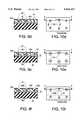
- FIGS. 9a-9f and 10a-10fdepict an alternative group of steps for providing the cathode structure of FIGS. 1e and 2e with a self-aligned gate structure.
- Porous layer 34Ais again formed with an inorganic glass.
- the thickness of layer 24Ais typically 0.5 micron.
- the first step for creating the gate structure in the alternative processis to electrochemically deposit caps 32 on filaments 30 in the same manner as described above. See FIGS. 9a and 10a which are respectively the same as FIGS. 7a and 8a. Caps 32 again consist of silver.
- a blanket layer 40 of electrically conductive gate materialis deposited on porous layer 24A and caps 32 along the top of the structure. See FIGS. 9b and 10b.
- the thickness of layer 40is typically 0.1 micron.
- the gate materialconsists of a metal selectively etchable with respect to the cap metal. Platinum can be utilized for the gate metal.
- the technique employed for the gate-metal depositionis not particularly important as long as the thickness of the portion of gate-metal layer 40 above porous layer 24A is relatively uniform.
- FIGS. 9c and 10cdepict the resulting structure in which items 32A are the remainders of caps 32. Item 40A is the remainder of gate-metal layer 40.
- the planarization operationis performed in several steps. Firstly, a flowable material such as photoresist is deposited on the top of the structure. Secondly, the flowable material is flowed so that its upper surface becomes largely planar. Thirdly, an etchback is performed with an etchant that attacks the flowable material and the gate metal at approximately the same rate. The etchback is terminated when all of the flowable material has been removed. Because the etchant attacks the gate metal at approximately the same rate as the flowable material, the upward-protruding portions of gate-metal layer 40--i.e., the portions overlying caps 32--are simultaneously removed.
- Caps 32Aare removed with an etchant that does not significantly attack filaments 30 or metal layer 40A. See FIGS. 9d and 10d.
- Layer 40Awhich now constitutes the gate electrode for the structure, has openings 42 respectively centered on filaments 30. Because each cap 32 was wider than corresponding filament 30, gate layer 40A is laterally separated from filaments 30.
- the cathode/gate structure of FIGS. 9d and 10dcan be directly employed as a field emitter. However, it is similarly advantageous to further process the cathode/gate structure of FIGS. 9d and 10d in the same manner as that of FIG. 7d and 8d. Accordingly, portions of porous layer 24A exposed through openings 42 are removed with an isotropic etchant to form cavities 44 around filaments 30 as shown in FIGS. 9e and 10e. Filaments 30 protrude outward beyond the remainder 24E of porous layer 24A. Each cavity 44 is considerably wider than corresponding pore 28 1 .
- Cavities 44typically extend partway down to lower conductive region 22.
- FIG. 9eillustrates this situation.
- cavities 44can also extend fully down to conductive region 22.
- An electropolishing and etching operationis performed to adjust and sharpen the upper ends of filaments 30. See FIGS. 9f and 10f. Items 30B again are the sharpened remainders of filaments 30.
- An additional electropolishing stepis typically also done to round the edges of patterned gate layer 40A overlying cavities 44. Item 40B in FIGS. 9f and 10f is the edge-rounded remainder of gate layer 40A.
- FIGS. 11a-11j and 12a-12jillustrate a further procedure for manufacturing a gated field-emission structure according to the teachings of the invention.
- This field emitteris structurally similar to both that of FIGS. 7f and 8f and that of FIGS. 9f and 10f.
- the field emitter fabricated according to the process of FIGS. 11a-11j and 12a-12jis typically used for exciting phosphors in a flat-panel television.
- the starting point againis insulating substrate 20 over which lower conductive region 22 is provided. See FIGS. 11a and 12a.
- Substrate 20 and region 22have the characteristics given above.
- region 22typically contains a group of largely parallel lines, two of which are shown in FIG. 12a.
- Insulating layer 24is again formed on top of the structure. See FIGS. 11b and 12b. Layer 24 likewise has the characteristics given above since charged-particle tracks are later formed through it.
- a blanket electrically conductive layer 46which later becomes the gate electrode, is formed on the top of insulating layer 24 as indicated in FIG. 11b.
- Conductive layer 46is typically 0.05 micron in thickness.
- Layer 46consists of a metal such as molybdenum, copper, or aluminum.
- the method for creating layer 48is not particularly critical as long as its thickness is relatively uniform.
- Layer 46is typically formed by a physical vapor deposition technique.
- a further electrically insulating layer 48is formed on the top of conductive layer 46. Again see FIG. 11b. Insulating layer 48 is in the range of 0.2-0.5 microns in thickness. As with insulating layer 24, layer 48 consists of (a) an organic polymer such as polycarbonate, polystyrene, or cellulose acetate, (b) an inorganic glass such as phosphate, quartz, or soda-lime glass, or (c) a crystal such as mica or quartz. Although there are some implementations in which layer 48 consists of the same insulator as layer 24, layer 48 is normally formed with an insulator that is selectively etchable with respect to layer 24.
- the structureis now subjected to energetic charged particles that impinge on the top of insulating layer 48 in a direction largely perpendicular to the (unshown) flat lower surface of substrate 20 and thus in a direction generally perpendicular to the upper structural surface.
- the charged particlespass through layers 48, 46, and 24 and into the underlying material to form straight tracks through insulating layers 24 and 48 at random locations.
- FIGS. 11c and 12cillustrate the track formation.
- the charged-particle tracksagain constitute damaged zones along the particle paths.
- the charged-particle tracksare indicated by reference symbols beginning with "50” in FIGS. 11c and 12c.
- Each trackis divided into (a) a "50A” segment extending through insulating layer 24 and (b) a "50B” segment extending through insulating layer 48 in a straight line with the 50A segment.
- the tracksfall into two categories: (a) segments 50A 1 and 50B 1 (collectively “50 1 ”) extending respectively through portions of layers 24 and 48 overlying lower conductive region 22 and (b) segments 50A 2 and 50B 2 (collectively "50 2 ”) extending respectively through portions of layers 24 and 48 not overlying region 22.
- charged-particle tracks 50 1 and 50 2extend parallel to one another in a direction generally perpendicular to the upper structural surface.
- Tracks 50have the same characteristics--e.g., size and spacing--as tracks 26.
- Tracks 50are also formed in the same way as tracks 26. To simplify the illustration, only a small portion of tracks 50 are indicated in FIGS. 11c and 12c.
- the damaged insulating material along track segments 50B in insulating layer 48is removed by bringing layer 48 into contact with a suitable chemical etchant that attacks the damaged 50B track material much more than the undamaged material of layer 48. As a result, generally circular pores are etched through layer 48 along segments 50B down to metal layer 46.
- the etchantpreferably does not significantly attack any of the other parts of the field-emission structure.
- the etchis continued into the largely undamaged material of insulating layer 48 to broaden the pores. Apertures 52 1 and 52 2 are thereby respectively created along track segments 50B 1 and 50B 2 . See FIGS. 11d and 12d. Apertures 52 1 and 52 2 (collectively "52") expose corresponding portions of the upper surface of metal layer 46. The etch is performed in a laterally uniform manner. Accordingly, each aperture 52 is centered on the location of corresponding track segment 50B. The thickness of layer 48 is also reduced during the etch.
- Apertures 52are generally circular in shape as viewed from the top in the plan view of FIG. 12d. Apertures 52 are also usually somewhat wider at the top than at the bottom as indicated in FIG. 11d. The reason for slanting apertures 52 in this way is to facilitate subsequent reactive-ion etching of metal layer 46.
- the second part of the insulating-material etchcan be done with the etchant used during the first part or with another etchant. In either case, components 20, 22, 24, and 46 are not significantly attacked during the second part of the etch. Apertures 52 thereby reach an average diameter of 15-300, typically 140 nm, along the bottom of the reduced-thickness remainder 48A of insulating layer 48.
- FIGS. 11e and 12edepict the consequent structure in which openings 54 1 extend through the portions of layer 46 located above lower conductive region 22, while openings 54 2 extend through the portions of layer 46 not overlying region 22.
- the remainder 46A of layer 46is the patterned gate electrode for the field emitter.
- the anisotropic etchis typically done according to a reactive-ion-etch technique.
- each opening 54is of largely the same transverse shape--i.e. generally circular-and of nearly the same diameter as corresponding aperture 52 (along the bottom of insulating layer 48A).
- Each opening 54is vertically aligned with corresponding aperture 52. Since each aperture 52 is centered on the location of corresponding track segment 50B, each opening 54 is also centered on the location of corresponding segment 50B.
- Insulating layer 48Ais usually removed at some point subsequent to the creation of openings 54. As, for example, indicated in FIGS. 11f and 12f, layer 48A could be removed directly after openings 54 are formed.
- Pores 28 1 and 28 2are thereby created through layer 24 respectively along track segments 50A 1 and 50A 2 as indicated in FIGS. 11g and 12g.
- Pores 28 1 and 28 2(again collectively "28") have the same physical/spatial characteristics, described above, as pores 28 in the previous manufacturing processes of the invention.
- the etch utilized to create pores 28 hereis typically performed in the same manner as described above in connection with the structure of FIGS. 1d and 2d.
- the remainder of layer 24again is porous insulating layer 24A.
- each pore 28 in FIGS. 11g and 12gis considerably narrower than corresponding opening 54.
- corresponding pore 28typically has a diameter of 100 nm.
- Each pore 28is centered on the location of corresponding track segment 50A. Because (a) each track segment 50B was in a straight line with corresponding track segment 50A and (b) each opening 54 is centered on the location of corresponding track segment 50B, each opening 54 is centered on corresponding pore 28.
- a suitable filament metalis now electrochemically deposited to form electron-emissive metal filaments 30 in pores 28 1 overlying lower conductive region 22 as indicated in FIGS. 11h and 12h.
- the depositionis performed in the manner prescribed above in connection with the structure of FIGS. 1e and 2e. Since there is no electrical contact at the bottoms of pores 28 2 located directly above substrate 20, substantially none of the filament metal accumulates in pores 28 2 .
- the dark circlesindicate pores 28 1 filled with filaments 30, while the light circles indicate empty pores 28 2 .
- the electrochemical nature of the processenables the deposition to be selective.
- Filaments 30again have the characteristics described above. Since pores 28 1 are situated at random locations across porous layer 24, filaments 30 are again located in random places across layer 24. Due to the centering that results from the track formation and etching, filaments 30 are self-aligned to openings 54 1 and therefore to gate electrode 46A.
- the cathode/gate structure of FIGS. 11h and 12hcan be utilized directly as a field emitter. Nonetheless, it is again advantageous for filaments 30 to have sharpened tips that protrude out of the porous material. Accordingly, the structure of FIGS. 11h and 12h is further processed in the way described above for the other gated field emitters of the invention.
- FIGS. 11i and 12iPortions of porous layer 24A exposed through openings 54 1 are removed with an isotropic etchant to form cavities 56 1 around filaments 30 as indicated in FIGS. 11i and 12i. Because gate layer 46A also has openings 54 2 , portions of layer 24A exposed through openings 54 2 are simultaneously removed to form cavities 56 2 . Cavities 56 1 and 56 2 (collectively "56") can extend partway, or all the way, down to lower conductive region 22. FIG. 11i indicates the former case. In both cases, filaments 30 now protrude outward beyond the remainder 24F of porous layer 24A.
- FIGS. 11j and 12jshow the final structure in which items 30B are the sharpened remainders of filaments 30. Item 46B is the edge-rounded remainder of gate layer 46A.
- Openings 54can alternatively be created by etching through holes whose diameter is considerable smaller than openings 54 rather than using apertures 52 whose diameter is approximately the same as openings 54.
- relatively narrow pores 58 1are created along track segments 50B 1 by bringing the structure into contact with an etchant that attacks the damaged material of insulating layer 48 much more than the undamaged material. Pores 58 1 extend down to metal layer 46 as depicted in FIG. 13a. Relatively narrow pores 58 2 (not shown) are similarly created along track segments 50B 2 down to region 46. Item 48B in FIG. 13a is the remainder of insulating layer 48.
- the portions of metal layer 46 exposed through pores 58 1are then removed with an isotropic etchant that attacks metal layer 46 much more than insulating layers 24 and 48B to form openings 54 1 down to layer 24. Due to the isotropic nature of the etch, openings 54 1 extend slightly under layer 48B as shown in FIG. 13b.
- the portions of layer 46 exposed through openings 58 2are simultaneously removed to create openings 54 2 (not shown) in the same way as openings 54 1 .
- Item 46Ais again the remainder of layer 46. From this point on, the structure is further processed in the manner described above for FIGS. 11f-11j.
- FIGS. 14 and 15illustrate the starting point for manufacturing certain implementations of the present field emitter in which lower conductive region 22 consists of a highly conductive layer 22A situated under a highly resistive (but still conductive) layer 22B. As shown in FIG. 15, each of the lines that form region 22 consists of segments of both of layers 22A and 22B.
- Highly conductive layer 22Aconsists of one or more of the materials described above for layer 22.
- Resistive layer 22Bis typically formed with cermet or doped polycrystalline silicon.
- FIGS. 16.1 and 16.2depict how the final structures of, for example, FIGS. 3b and 11j appear when lower conductive region 22 consists of highly conductive layer 22A and highly resistive layer 22B.
- the lower ends of sharpened filaments 30A or 30Bcontact resistive layer 22B.
- the resistance between each filament 30A or 30B and layer 22Ais typically 100 megaohms.
- FIGS. 11a-11j and 12a-12jcan be readily extended to create a gated field-emission structure having one or more additional control electrodes above the gate electrode.
- FIGS. 17a-17lthey illustrate how a gated field emitter having a focusing control electrode is so manufactured. This field emitter is also suitable for flat-panel television applications.
- the field emitteris built on insulating substrate 20 over which lower conductive region 22 is provided as shown in FIG. 17a.
- Insulating layer 24, metal layer 46, and second insulating layer 48are formed in sequence on the top of the structure. See FIG. 17b.
- Components 20, 22, 24, 46, and 48all have the characteristics described above.
- a second electrically conductive layer 60is formed on the top of second insulating layer 48.
- Conductive layer 60later becomes the focusing electrode.
- a further electrically insulating layer 62is formed on the top of layer 60.
- Layers 62 and 60respectively have largely the same characteristics as insulating layer 48 and metal layer 46. Accordingly, layer 60 consists of insulating material, and layer 62 consists of metal.
- the structureis subjected to energetic charged particles traveling in a direction largely perpendicular to the (unshown) lower substrate surface and thus in a direction generally perpendicular to the upper structural surface.
- the charged particlespass through layers 62, 60, 48, 46, and 24 and into the underlying material to form straight tracks through insulating layers 62, 48, and 24. See FIG. 17c.
- Each trackis divided into (a) a "64A” segment extending through insulating layer 24, (b) a “64B” segment extending through insulating layer 48, and (c) a "64C” segment extending through insulating layer 62.
- the charged particlesdo not cause any significant damage to metal layers 60 and 46 and therefore do not create any tracks through layers 60 and 46.
- the tracksfall into two categories: (a) segments 64A 1 , 64B 1 , and 64C 1 (collectively “64 1 ”) extending respectively through portions of layers 24, 48, and 62 overlying lower conductive region 22, and (b) segments 64A 2 , 64B 2 , and 64C 2 (collectively "64 2 ") extending respectively through portions of layers 24, 48, and 62 not overlying region 22.
- Track segments 64 2although not shown in the drawings, are analogous to track segments 50 2 --i.e., segments 50B 2 and 50A 2 --depicted in FIGS. 12c and 12e for the previous manufacturing process of the invention.
- Charged-particle tracks 64 1 and 64 2extend parallel to one another in a direction generally perpendicular to the upper structural surface. Tracks 64 have the same basic characteristics, and are formed in the same way, as tracks 50 and 26 described above.
- Generally circular poresare formed through insulating layer 62 along track segments 64C down to metal layer 60 by bringing layer 62 into contact with a chemical etchant that attacks the damaged 64C track material much more than the undamaged material of layer 62.
- the poresare then broadened by continuing the etch into the undamaged material to form apertures 66 1 and 66 2 respectively along the pores created by etching tracks 64B 1 and 64B 2 . See FIG. 17d.
- Apertures 66 2although not shown in the drawings, are analogous to apertures 52 2 depicted in FIG. 12d.
- apertures 66 1 and 66 2are formed uniformly in largely the same manner as that described above for creating apertures 52, with one notable difference.
- the etch time for apertures 66is somewhat longer than the etch time for apertures 52. Consequently, apertures 66 have substantially the same characteristics as apertures 52 but are larger in diameter. In particular, apertures 66 reach an average diameter of 20-400 nm, typically 190 nm, along the bottom of the remainder 62A of insulating layer 62.
- openings 68 1are thereby created down to insulating layer 48 through the portions of layer 60 overlying lower conductive region 22 as shown in FIG. 17e.
- Openings 68 2are simultaneously created down to layer 48 through portions of layer 60 not overlying region 22.
- openings 68 2are analogous to openings 54 2 depicted in FIG. 12e.
- the remainder 60A of metal layer 60 in FIG. 17eis the patterned focusing electrode for the field emitter.
- openings 68 1 and 68 2are typically performed in the same way as the metal etch employed to create openings 54 in the previous fabrication process of the invention. As a result, each opening 68 is centered on the location of corresponding track segment 64C.
- Insulating layer 62Ais normally removed at some point after openings 68 are created. This can, for example, be done directly after the formation of openings 68.
- FIG. 17fshows the resultant structure.
- poresare created in the damaged insulating material along segments 64B by bringing the structure into contact with a chemical etchant that attacks the damaged 64B track material much more than the undamaged material of layer 48. The etch is continued into the undamaged insulating material of layer 48 to broaden the pores. Apertures 70 1 and 70 2 are thereby created respectively along track segments 64B 1 and 64B 2 . See FIG. 17g. Although not shown in the drawings, apertures 70 2 are analogous to apertures 52 2 shown in FIG. 12d. Item 48B in FIG. 17g is the remainder of layer 48.
- apertures 70 1 and 70 2are performed uniformly in the manner described above for etching apertures 52 in the previous manufacturing process of the invention. Accordingly, apertures 70 have substantially the same characteristics as apertures 52, including the same average aperture diameter.
- the portions of metal layer 46 exposed via apertures 70 1are removed with an anisotropic etchant to create generally circular openings 54 1 down to portions of insulating layer 24 that overlie lower conductive region 22 as shown in FIG. 17h.
- the portions of layer 46 exposed via apertures 70 2are simultaneously removed to create generally circular openings 54 2 down to the portions of layer 24 situated directly above region 22.
- openings 54 2are analogous to openings 54 2 depicted in FIG. 12g.
- the remaining portion 46A of gate layer 46 in FIG. 17his again the gate electrode for the field emitter.
- each opening 54is centered on the location of corresponding track segment 64B.
- FIG. 17his substantially the same as the structure of FIG. 11f.
- Track segments 64A 1 in FIG. 17hare the same as track segments 50A 1 in FIG. 11f.
- the structure of FIG. 17his further processed in the same way as the structure of FIG. 11f.
- FIGS. 17i-17lrespectively correspond to FIGS. 11g-11j. The processing description presented above in connection with FIGS. 11g-11j applies directly to FIGS. 17i-17l with each track segment "50A" now being referred to as "64A".
- insulating layer 48B below the edges of focusing electrode 60Aare partially etched back. Depending on the properties of layers 48B and 24A, this etchback is either performed during the etch to create cavities 56 in porous insulating layer 24A or as a separate step. As indicated in FIG. 17k, the edges of layer 60A extend laterally beyond the remainder 48C of insulating layer 48B. Item 24F is again the remainder of porous layer 24A.
- edges of focusing layer 60Aare typically rounded during the same electropolishing step used to round the edges of gate layer 46A.
- Item 60B in FIG. 17lis the rounded-edge patterned remainder of focusing layer 60A.
- Item 46Bis again the rounded-edge patterned remainder of gate layer 46A.
- items 30Bare again the sharpened filaments.
- Lower conductive region 22 in FIG. 17 lmay again consist of highly resistive layer 22A and overlying highly conductive layer 22B as described above. Also, the steps employed to create focusing electrode 60B above insulating layer 46B can be repeated to create one or more further control electrodes above layer 60B. In doing so, the centering that results from the track formation and etching enables each further control electrode to be self-aligned to filaments 30B.
- FIGS. 18.1-18.4illustrate several longitudinal shapes that filaments 30A or 30B can have in the present invention.
- filaments 30A/30Bcan be solid cylinders except at their upper ends. If tracks 26 are etched in such a manner as to create pores 28 as cones, filaments 30A/30B can be solid cones which taper down in transverse cross section from just below their upper ends to their lower ends in the manner shown in FIGS. 18.3 and 18.4.
- the electron-emissive tips at the upper ends of filaments 30A/30Bcan be generally rounded as indicated in FIGS. 18.1 and 18.3 or sharply pointed as indicated in FIGS. 18.2 and 18.4.
- FIG. 19depicts the electrochemical deposition system employed during the electrochemical deposition operations described above.
- the electrochemical systemconsists of an electrochemical cell 72 and a power supply and control system 74.
- electrochemical cell 72consists of cell electrolyte 76, a surrounding sidewall 78, an O-ring 80, an anode 82, and a cathode 84 formed by part of the structure on which metal is being deposited.
- cathode 84includes lower conductive substrate 20 to which power supply and control system 74 is connected.
- FIG. 19specifically illustrates the filament deposition. The set-up is the same for the cap deposition.
- the electrochemical system shown in FIG. 19operates according to a constant-current technique.
- a constant-voltage electrochemical deposition systemcould be used.
- the field emitters of the present inventionoperate in the following way.
- An anode (or collector) structureis situated a short distance away from the top of each field emitter.
- a voltageis applied between a selected part of the anode and a selected one of the lines that forms lower conductive region 22.
- the particular filaments 30 above the selected linethen emit electrons collected at the anode structure.
- the gate electrode in the gated implementationsis used to extract electrons from the filaments and control the magnitude of the electron beam.
- the focusing electrodewhen present, focuses the electron beam.
- substrate 20could be deleted if lower conductive region 22 is a continuous layer of sufficient thickness to support the structure.
- Insulating substrate 20could be replaced with a composite substrate in which a thin insulating layer overlies a relatively thick non-insulating layer that furnishes the necessary structural support.
- Substrate 20 and/or conductive region 22could be formed under insulating layer 24 after charged-particle tracks 26 are formed through it.
- Gate layer 34B, 40B or 46Bcould be patterned into lines running perpendicular to the lines that form region 22.
- electrochemical depositionscould be performed by a full immersion technique with the sides of the field emitter suitably protected to avoid unwanted deposition.
- Thermal annealingcould be used to modify the filament shape.
Landscapes
- Engineering & Computer Science (AREA)
- Chemical & Material Sciences (AREA)
- Nanotechnology (AREA)
- Manufacturing & Machinery (AREA)
- Physics & Mathematics (AREA)
- Mathematical Physics (AREA)
- Theoretical Computer Science (AREA)
- Crystallography & Structural Chemistry (AREA)
- Cold Cathode And The Manufacture (AREA)
- Cathode-Ray Tubes And Fluorescent Screens For Display (AREA)
Abstract
Description
Claims (82)
Priority Applications (23)
| Application Number | Priority Date | Filing Date | Title |
|---|---|---|---|
| US08/118,490US5462467A (en) | 1993-09-08 | 1993-09-08 | Fabrication of filamentary field-emission device, including self-aligned gate |
| US08/158,102US5559389A (en) | 1993-09-08 | 1993-11-24 | Electron-emitting devices having variously constituted electron-emissive elements, including cones or pedestals |
| US08/269,229US5564959A (en) | 1993-09-08 | 1994-06-29 | Use of charged-particle tracks in fabricating gated electron-emitting devices |
| PCT/US1994/009762WO1995007543A1 (en) | 1993-09-08 | 1994-09-08 | Fabrication and structure of electron-emitting devices having high emitter packing density |
| JP50871395AJP3699114B2 (en) | 1993-09-08 | 1994-09-08 | Structure of electron-emitting device with high packing density |
| DE69435269TDE69435269D1 (en) | 1993-09-08 | 1994-09-08 | Fabrication and structure of electron emitter devices with high emitter packing density |
| HK98116148.0AHK1015188B (en) | 1993-09-08 | 1994-09-08 | Fabrication of electron-emitting devices having high emitter packing density |
| EP94927275AEP0717877B1 (en) | 1993-09-08 | 1994-09-08 | Fabrication of electron-emitting devices having high emitter packing density |
| AU76770/94AAU7677094A (en) | 1993-09-08 | 1994-09-08 | Fabrication and structure of electron-emitting devices having high emitter packing density |
| DE69421711TDE69421711T2 (en) | 1993-09-08 | 1994-09-08 | MANUFACTURE OF ELECTRON-EMITTING DEVICES WITH HIGH EMITTER PACKING DENSITY |
| EP99108617AEP0945885B1 (en) | 1993-09-08 | 1994-09-08 | Fabrication and structure of electron-emitting devices having high emitter packing density |
| US08/383,409US7025892B1 (en) | 1993-09-08 | 1995-01-31 | Method for creating gated filament structures for field emission displays |
| US08/383,410US5801477A (en) | 1993-09-08 | 1995-01-31 | Gated filament structures for a field emission display |
| US08/383,408US5578185A (en) | 1993-09-08 | 1995-01-31 | Method for creating gated filament structures for field emision displays |
| US08/446,392US5851669A (en) | 1993-09-08 | 1995-05-22 | Field-emission device that utilizes filamentary electron-emissive elements and typically has self-aligned gate |
| US08/447,470US5562516A (en) | 1993-09-08 | 1995-05-22 | Field-emitter fabrication using charged-particle tracks |
| US08/568,885US5827099A (en) | 1993-09-08 | 1995-12-07 | Use of early formed lift-off layer in fabricating gated electron-emitting devices |
| US08/678,565US5813892A (en) | 1993-09-08 | 1996-07-12 | Use of charged-particle tracks in fabricating electron-emitting device having resistive layer |
| US08/725,941US5665421A (en) | 1993-09-08 | 1996-10-08 | Method for creating gated filament structures for field emission displays |
| US08/855,425US5913704A (en) | 1993-09-08 | 1997-05-12 | Fabrication of electronic devices by method that involves ion tracking |
| US09/107,392US6204596B1 (en) | 1993-09-08 | 1998-06-30 | Filamentary electron-emission device having self-aligned gate or/and lower conductive/resistive region |
| US09/141,697US6515407B1 (en) | 1993-09-08 | 1998-08-28 | Gated filament structures for a field emission display |
| JP2005135104AJP3793219B2 (en) | 1993-09-08 | 2005-05-06 | Manufacturing method of electron-emitting device with high packing density |
Applications Claiming Priority (1)
| Application Number | Priority Date | Filing Date | Title |
|---|---|---|---|
| US08/118,490US5462467A (en) | 1993-09-08 | 1993-09-08 | Fabrication of filamentary field-emission device, including self-aligned gate |
Related Child Applications (4)
| Application Number | Title | Priority Date | Filing Date |
|---|---|---|---|
| US08/158,102Continuation-In-PartUS5559389A (en) | 1993-09-08 | 1993-11-24 | Electron-emitting devices having variously constituted electron-emissive elements, including cones or pedestals |
| US08/269,229Continuation-In-PartUS5564959A (en) | 1993-09-08 | 1994-06-29 | Use of charged-particle tracks in fabricating gated electron-emitting devices |
| US08/446,392DivisionUS5851669A (en) | 1993-09-08 | 1995-05-22 | Field-emission device that utilizes filamentary electron-emissive elements and typically has self-aligned gate |
| US08/447,470ContinuationUS5562516A (en) | 1993-09-08 | 1995-05-22 | Field-emitter fabrication using charged-particle tracks |
Publications (1)
| Publication Number | Publication Date |
|---|---|
| US5462467Atrue US5462467A (en) | 1995-10-31 |
Family
ID=22378922
Family Applications (3)
| Application Number | Title | Priority Date | Filing Date |
|---|---|---|---|
| US08/118,490Expired - LifetimeUS5462467A (en) | 1993-09-08 | 1993-09-08 | Fabrication of filamentary field-emission device, including self-aligned gate |
| US08/446,392Expired - LifetimeUS5851669A (en) | 1993-09-08 | 1995-05-22 | Field-emission device that utilizes filamentary electron-emissive elements and typically has self-aligned gate |
| US09/107,392Expired - LifetimeUS6204596B1 (en) | 1993-09-08 | 1998-06-30 | Filamentary electron-emission device having self-aligned gate or/and lower conductive/resistive region |
Family Applications After (2)
| Application Number | Title | Priority Date | Filing Date |
|---|---|---|---|
| US08/446,392Expired - LifetimeUS5851669A (en) | 1993-09-08 | 1995-05-22 | Field-emission device that utilizes filamentary electron-emissive elements and typically has self-aligned gate |
| US09/107,392Expired - LifetimeUS6204596B1 (en) | 1993-09-08 | 1998-06-30 | Filamentary electron-emission device having self-aligned gate or/and lower conductive/resistive region |
Country Status (2)
| Country | Link |
|---|---|
| US (3) | US5462467A (en) |
| DE (1) | DE69435269D1 (en) |
Cited By (40)
| Publication number | Priority date | Publication date | Assignee | Title |
|---|---|---|---|---|
| WO1997046739A1 (en)* | 1996-06-07 | 1997-12-11 | Candescent Technologies Corporation | Method of fabricating an electron-emitting device |
| WO1997047021A1 (en)* | 1996-06-07 | 1997-12-11 | Candescent Technologies Corporation | Fabrication of gated electron-emitting device utilizing distributed particles to define gate openings |
| US5697827A (en)* | 1996-01-11 | 1997-12-16 | Rabinowitz; Mario | Emissive flat panel display with improved regenerative cathode |
| US5766446A (en)* | 1996-03-05 | 1998-06-16 | Candescent Technologies Corporation | Electrochemical removal of material, particularly excess emitter material in electron-emitting device |
| US5813892A (en)* | 1993-09-08 | 1998-09-29 | Candescent Technologies Corporation | Use of charged-particle tracks in fabricating electron-emitting device having resistive layer |
| US5831392A (en)* | 1996-10-31 | 1998-11-03 | Candescent Technologies Corporation | Device for conditioning control signal to electron emitter, preferably so that collected electron current varies linearly with input control voltage |
| US5865657A (en)* | 1996-06-07 | 1999-02-02 | Candescent Technologies Corporation | Fabrication of gated electron-emitting device utilizing distributed particles to form gate openings typically beveled and/or combined with lift-off or electrochemical removal of excess emitter material |
| US5865659A (en)* | 1996-06-07 | 1999-02-02 | Candescent Technologies Corporation | Fabrication of gated electron-emitting device utilizing distributed particles to define gate openings and utilizing spacer material to control spacing between gate layer and electron-emissive elements |
| US5882503A (en)* | 1997-05-01 | 1999-03-16 | The Regents Of The University Of California | Electrochemical formation of field emitters |
| US5891321A (en)* | 1997-05-01 | 1999-04-06 | The Regents Of The University Of California | Electrochemical sharpening of field emission tips |
| WO1999006844A3 (en)* | 1997-07-30 | 1999-04-08 | Candescent Tech Corp | Magnetic current sensing and short circuit detection in plate structure |
| US5893967A (en)* | 1996-03-05 | 1999-04-13 | Candescent Technologies Corporation | Impedance-assisted electrochemical removal of material, particularly excess emitter material in electron-emitting device |
| US5913704A (en)* | 1993-09-08 | 1999-06-22 | Candescent Technologies Corporation | Fabrication of electronic devices by method that involves ion tracking |
| US5947783A (en)* | 1996-11-01 | 1999-09-07 | Si Diamond Technology, Inc. | Method of forming a cathode assembly comprising a diamond layer |
| US6007695A (en)* | 1997-09-30 | 1999-12-28 | Candescent Technologies Corporation | Selective removal of material using self-initiated galvanic activity in electrolytic bath |
| US6008062A (en)* | 1997-10-31 | 1999-12-28 | Candescent Technologies Corporation | Undercutting technique for creating coating in spaced-apart segments |
| US6010383A (en)* | 1997-10-31 | 2000-01-04 | Candescent Technologies Corporation | Protection of electron-emissive elements prior to removing excess emitter material during fabrication of electron-emitting device |
| US6024622A (en)* | 1997-03-24 | 2000-02-15 | Sony Corporation | Field emission type emitter |
| US6033583A (en)* | 1997-05-05 | 2000-03-07 | The Regents Of The University Of California | Vapor etching of nuclear tracks in dielectric materials |
| US6045678A (en)* | 1997-05-01 | 2000-04-04 | The Regents Of The University Of California | Formation of nanofilament field emission devices |
| US6046539A (en)* | 1997-04-29 | 2000-04-04 | Candescent Technologies Corporation | Use of sacrificial masking layer and backside exposure in forming openings that typically receive light-emissive material |
| US6064145A (en)* | 1999-06-04 | 2000-05-16 | Winbond Electronics Corporation | Fabrication of field emitting tips |
| US6107806A (en)* | 1997-07-30 | 2000-08-22 | Candescent Technologies Corporation | Device for magnetically sensing current in plate structure |
| DE19910156A1 (en)* | 1999-02-26 | 2000-09-07 | Hahn Meitner Inst Berlin Gmbh | Electron emitter and method for its production |
| US6118279A (en)* | 1997-07-30 | 2000-09-12 | Candescent Technologies Corporation | Magnetic detection of short circuit defects in plate structure |
| US6120674A (en)* | 1997-06-30 | 2000-09-19 | Candescent Technologies Corporation | Electrochemical removal of material in electron-emitting device |
| US6124670A (en)* | 1998-05-29 | 2000-09-26 | The Regents Of The University Of California | Gate-and emitter array on fiber electron field emission structure |
| US6187603B1 (en) | 1996-06-07 | 2001-02-13 | Candescent Technologies Corporation | Fabrication of gated electron-emitting devices utilizing distributed particles to define gate openings, typically in combination with lift-off of excess emitter material |
| US6193870B1 (en)* | 1997-05-01 | 2001-02-27 | The Regents Of The University Of California | Use of a hard mask for formation of gate and dielectric via nanofilament field emission devices |
| US6356014B2 (en)* | 1997-03-27 | 2002-03-12 | Candescent Technologies Corporation | Electron emitters coated with carbon containing layer |
| US6440763B1 (en) | 2001-03-22 | 2002-08-27 | The United States Of America As Represented By The Secretary Of The Navy | Methods for manufacture of self-aligned integrally gated nanofilament field emitter cell and array |
| US6444256B1 (en) | 1999-11-17 | 2002-09-03 | The Regents Of The University Of California | Formation of nanometer-size wires using infiltration into latent nuclear tracks |
| US6448701B1 (en) | 2001-03-09 | 2002-09-10 | The United States Of America As Represented By The Secretary Of The Navy | Self-aligned integrally gated nanofilament field emitter cell and array |
| WO2002037564A3 (en)* | 2000-10-30 | 2002-11-07 | Schwerionenforsch Gmbh | Film material comprising metal spikes and method for the production thereof |
| US6503409B1 (en)* | 2000-05-25 | 2003-01-07 | Sandia Corporation | Lithographic fabrication of nanoapertures |
| US20050062033A1 (en)* | 2003-08-08 | 2005-03-24 | Canon Kabushiki Kaisha | Structure and method for production of the same |
| US7025892B1 (en)* | 1993-09-08 | 2006-04-11 | Candescent Technologies Corporation | Method for creating gated filament structures for field emission displays |
| US20070293116A1 (en)* | 2001-06-29 | 2007-12-20 | Canon Kabushiki Kaisha | Electron-emitting device, electron source, and image-forming apparatus |
| US8168380B2 (en) | 1997-02-12 | 2012-05-01 | Life Technologies Corporation | Methods and products for analyzing polymers |
| US20140033374A1 (en)* | 2012-07-27 | 2014-01-30 | Academia Sinica | System for fabricating nanoscale probe and method thereof |
Families Citing this family (17)
| Publication number | Priority date | Publication date | Assignee | Title |
|---|---|---|---|---|
| US6861791B1 (en)* | 1998-04-30 | 2005-03-01 | Crystals And Technologies, Ltd. | Stabilized and controlled electron sources, matrix systems of the electron sources, and method for production thereof |
| US7002287B1 (en)* | 1998-05-29 | 2006-02-21 | Candescent Intellectual Property Services, Inc. | Protected substrate structure for a field emission display device |
| WO2001018866A1 (en)* | 1999-09-10 | 2001-03-15 | Starmega Corporation | Strongly textured atomic ridges and dots |
| US7064500B2 (en)* | 2000-05-26 | 2006-06-20 | Exaconnect Corp. | Semi-conductor interconnect using free space electron switch |
| US6407516B1 (en) | 2000-05-26 | 2002-06-18 | Exaconnect Inc. | Free space electron switch |
| US6800877B2 (en)* | 2000-05-26 | 2004-10-05 | Exaconnect Corp. | Semi-conductor interconnect using free space electron switch |
| US6545425B2 (en) | 2000-05-26 | 2003-04-08 | Exaconnect Corp. | Use of a free space electron switch in a telecommunications network |
| US6801002B2 (en)* | 2000-05-26 | 2004-10-05 | Exaconnect Corp. | Use of a free space electron switch in a telecommunications network |
| JP2003016921A (en)* | 2000-09-20 | 2003-01-17 | Canon Inc | Structure, electron-emitting device, image forming apparatus, and manufacturing method thereof |
| WO2003063120A1 (en)* | 2002-01-15 | 2003-07-31 | The Government Of The United States Of America, As Represented By The Secretary Of The Navy | Method and apparatus for regulating electron emission in field emitter devices |
| CN100530517C (en)* | 2004-12-08 | 2009-08-19 | 鸿富锦精密工业(深圳)有限公司 | Field emission illuminating light source |
| US20060151777A1 (en)* | 2005-01-12 | 2006-07-13 | Naberhuis Steven L | Multi-layer thin film in a ballistic electron emitter |
| SG140484A1 (en)* | 2006-08-24 | 2008-03-28 | Sony Corp | An electron emitter and a display apparatus utilizing the same |
| JP2010225297A (en)* | 2009-03-19 | 2010-10-07 | Futaba Corp | Method of manufacturing cold cathode electron source, and cold cathode electron source |
| US8536564B1 (en) | 2011-09-28 | 2013-09-17 | Sandia Corporation | Integrated field emission array for ion desorption |
| US8814622B1 (en) | 2011-11-17 | 2014-08-26 | Sandia Corporation | Method of manufacturing a fully integrated and encapsulated micro-fabricated vacuum diode |
| US10658144B2 (en)* | 2017-07-22 | 2020-05-19 | Modern Electron, LLC | Shadowed grid structures for electrodes in vacuum electronics |
Citations (29)
| Publication number | Priority date | Publication date | Assignee | Title |
|---|---|---|---|---|
| US3303085A (en)* | 1962-02-28 | 1967-02-07 | Gen Electric | Molecular sieves and methods for producing same |
| US3345181A (en)* | 1966-01-24 | 1967-10-03 | Hupp Corp | Method for roasting coffee beans and similar particulate solids |
| US3407125A (en)* | 1965-01-18 | 1968-10-22 | Corning Glass Works | Method of making filamentary metal structures |
| US3497929A (en)* | 1966-05-31 | 1970-03-03 | Stanford Research Inst | Method of making a needle-type electron source |
| US3562881A (en)* | 1969-02-27 | 1971-02-16 | Nasa | Field-ionization electrodes |
| US3665241A (en)* | 1970-07-13 | 1972-05-23 | Stanford Research Inst | Field ionizer and field emission cathode structures and methods of production |
| US3755704A (en)* | 1970-02-06 | 1973-08-28 | Stanford Research Inst | Field emission cathode structures and devices utilizing such structures |
| US4008412A (en)* | 1974-08-16 | 1977-02-15 | Hitachi, Ltd. | Thin-film field-emission electron source and a method for manufacturing the same |
| DE2951287A1 (en)* | 1979-12-20 | 1981-07-02 | Gesellschaft für Schwerionenforschung mbH, 6100 Darmstadt | METHOD FOR PRODUCING PLANE SURFACES WITH THE FINEST TIPS IN THE MICROMETER AREA |
| US4407934A (en)* | 1981-12-04 | 1983-10-04 | Burroughs Corporation | Method of making an assembly of electrodes |
| US4668957A (en)* | 1983-10-12 | 1987-05-26 | Gesellschaft f/u/ r Schwerionenforschung mbH Darmstadt | Amorphous glass matrix containing aligned microscopically thin metal conductors |
| US4732646A (en)* | 1986-03-27 | 1988-03-22 | International Business Machines Corporation | Method of forming identically positioned alignment marks on opposite sides of a semiconductor wafer |
| US4874981A (en)* | 1988-05-10 | 1989-10-17 | Sri International | Automatically focusing field emission electrode |
| EP0351110A1 (en)* | 1988-07-13 | 1990-01-17 | THORN EMI plc | Method of manifacturing a cold cathode, field emission device and a field emission device manufactured by the method |
| US4897338A (en)* | 1987-08-03 | 1990-01-30 | Allied-Signal Inc. | Method for the manufacture of multilayer printed circuit boards |
| US4940916A (en)* | 1987-11-06 | 1990-07-10 | Commissariat A L'energie Atomique | Electron source with micropoint emissive cathodes and display means by cathodoluminescence excited by field emission using said source |
| EP0416625A2 (en)* | 1989-09-07 | 1991-03-13 | Canon Kabushiki Kaisha | Electron emitting device, method for producing the same, and display apparatus and electron scribing apparatus utilizing same. |
| US5053673A (en)* | 1988-10-17 | 1991-10-01 | Matsushita Electric Industrial Co., Ltd. | Field emission cathodes and method of manufacture thereof |
| WO1992002030A1 (en)* | 1990-07-18 | 1992-02-06 | International Business Machines Corporation | Process and structure of an integrated vacuum microelectronic device |
| US5142184A (en)* | 1990-02-09 | 1992-08-25 | Kane Robert C | Cold cathode field emission device with integral emitter ballasting |
| US5150019A (en)* | 1990-10-01 | 1992-09-22 | National Semiconductor Corp. | Integrated circuit electronic grid device and method |
| US5150192A (en)* | 1990-09-27 | 1992-09-22 | The United States Of America As Represented By The Secretary Of The Navy | Field emitter array |
| US5164632A (en)* | 1990-05-31 | 1992-11-17 | Ricoh Company, Ltd. | Electron emission element for use in a display device |
| US5170092A (en)* | 1989-05-19 | 1992-12-08 | Matsushita Electric Industrial Co., Ltd. | Electron-emitting device and process for making the same |
| US5194780A (en)* | 1990-06-13 | 1993-03-16 | Commissariat A L'energie Atomique | Electron source with microtip emissive cathodes |
| US5199917A (en)* | 1991-12-09 | 1993-04-06 | Cornell Research Foundation, Inc. | Silicon tip field emission cathode arrays and fabrication thereof |
| US5211707A (en)* | 1991-07-11 | 1993-05-18 | Gte Laboratories Incorporated | Semiconductor metal composite field emission cathodes |
| DE4209301C1 (en)* | 1992-03-21 | 1993-08-19 | Gesellschaft Fuer Schwerionenforschung Mbh, 6100 Darmstadt, De | Manufacture of controlled field emitter for flat display screen, TV etc. - using successive etching and deposition stages to form cone shaped emitter peak set in insulating matrix together with electrodes |
| WO1993018536A1 (en)* | 1992-03-04 | 1993-09-16 | Mcnc | Vertical microelectronic field emission devices and methods of making same |
Family Cites Families (25)
| Publication number | Priority date | Publication date | Assignee | Title |
|---|---|---|---|---|
| JPS5325632B2 (en)* | 1973-03-22 | 1978-07-27 | ||
| US3970887A (en)* | 1974-06-19 | 1976-07-20 | Micro-Bit Corporation | Micro-structure field emission electron source |
| US4345181A (en)* | 1980-06-02 | 1982-08-17 | Joe Shelton | Edge effect elimination and beam forming designs for field emitting arrays |
| FR2561019B1 (en)* | 1984-03-09 | 1987-07-17 | Etude Surfaces Lab | PROCESS FOR PRODUCING FLAT VISUALIZATION SCREENS AND FLAT SCREENS OBTAINED BY IMPLEMENTING SAID METHOD |
| FR2568394B1 (en)* | 1984-07-27 | 1988-02-12 | Commissariat Energie Atomique | DEVICE FOR VIEWING BY CATHODOLUMINESCENCE EXCITED BY FIELD EMISSION |
| FR2593953B1 (en)* | 1986-01-24 | 1988-04-29 | Commissariat Energie Atomique | METHOD FOR MANUFACTURING A DEVICE FOR VIEWING BY CATHODOLUMINESCENCE EXCITED BY FIELD EMISSION |
| US5019003A (en)* | 1989-09-29 | 1991-05-28 | Motorola, Inc. | Field emission device having preformed emitters |
| US5007873A (en)* | 1990-02-09 | 1991-04-16 | Motorola, Inc. | Non-planar field emission device having an emitter formed with a substantially normal vapor deposition process |
| US5202571A (en)* | 1990-07-06 | 1993-04-13 | Canon Kabushiki Kaisha | Electron emitting device with diamond |
| DE4041276C1 (en)* | 1990-12-21 | 1992-02-27 | Siemens Ag, 8000 Muenchen, De | |
| GB9101723D0 (en)* | 1991-01-25 | 1991-03-06 | Marconi Gec Ltd | Field emission devices |
| JP2626276B2 (en)* | 1991-02-06 | 1997-07-02 | 双葉電子工業株式会社 | Electron-emitting device |
| JP2550798B2 (en)* | 1991-04-12 | 1996-11-06 | 富士通株式会社 | Micro cold cathode manufacturing method |
| US5249340A (en)* | 1991-06-24 | 1993-10-05 | Motorola, Inc. | Field emission device employing a selective electrode deposition method |
| US5129850A (en)* | 1991-08-20 | 1992-07-14 | Motorola, Inc. | Method of making a molded field emission electron emitter employing a diamond coating |
| US5141460A (en)* | 1991-08-20 | 1992-08-25 | Jaskie James E | Method of making a field emission electron source employing a diamond coating |
| US5199918A (en)* | 1991-11-07 | 1993-04-06 | Microelectronics And Computer Technology Corporation | Method of forming field emitter device with diamond emission tips |
| US5252833A (en)* | 1992-02-05 | 1993-10-12 | Motorola, Inc. | Electron source for depletion mode electron emission apparatus |
| KR950004516B1 (en)* | 1992-04-29 | 1995-05-01 | 삼성전관주식회사 | Field emission display and manufacturing method |
| US5278475A (en)* | 1992-06-01 | 1994-01-11 | Motorola, Inc. | Cathodoluminescent display apparatus and method for realization using diamond crystallites |
| KR950008756B1 (en)* | 1992-11-25 | 1995-08-04 | 삼성전관주식회사 | Silicon field emission device and manufacture mathode |
| JPH08507643A (en)* | 1993-03-11 | 1996-08-13 | フェド.コーポレイション | Emitter tip structure, field emission device including the emitter tip structure, and method of manufacturing the same |
| US5559389A (en)* | 1993-09-08 | 1996-09-24 | Silicon Video Corporation | Electron-emitting devices having variously constituted electron-emissive elements, including cones or pedestals |
| JP2699827B2 (en)* | 1993-09-27 | 1998-01-19 | 双葉電子工業株式会社 | Field emission cathode device |
| US5458520A (en)* | 1994-12-13 | 1995-10-17 | International Business Machines Corporation | Method for producing planar field emission structure |
- 1993
- 1993-09-08USUS08/118,490patent/US5462467A/ennot_activeExpired - Lifetime
- 1994
- 1994-09-08DEDE69435269Tpatent/DE69435269D1/ennot_activeExpired - Lifetime
- 1995
- 1995-05-22USUS08/446,392patent/US5851669A/ennot_activeExpired - Lifetime
- 1998
- 1998-06-30USUS09/107,392patent/US6204596B1/ennot_activeExpired - Lifetime
Patent Citations (32)
| Publication number | Priority date | Publication date | Assignee | Title |
|---|---|---|---|---|
| US3303085A (en)* | 1962-02-28 | 1967-02-07 | Gen Electric | Molecular sieves and methods for producing same |
| US3407125A (en)* | 1965-01-18 | 1968-10-22 | Corning Glass Works | Method of making filamentary metal structures |
| US3345181A (en)* | 1966-01-24 | 1967-10-03 | Hupp Corp | Method for roasting coffee beans and similar particulate solids |
| US3497929A (en)* | 1966-05-31 | 1970-03-03 | Stanford Research Inst | Method of making a needle-type electron source |
| US3562881A (en)* | 1969-02-27 | 1971-02-16 | Nasa | Field-ionization electrodes |
| US3755704A (en)* | 1970-02-06 | 1973-08-28 | Stanford Research Inst | Field emission cathode structures and devices utilizing such structures |
| US3665241A (en)* | 1970-07-13 | 1972-05-23 | Stanford Research Inst | Field ionizer and field emission cathode structures and methods of production |
| US4008412A (en)* | 1974-08-16 | 1977-02-15 | Hitachi, Ltd. | Thin-film field-emission electron source and a method for manufacturing the same |
| DE2951287A1 (en)* | 1979-12-20 | 1981-07-02 | Gesellschaft für Schwerionenforschung mbH, 6100 Darmstadt | METHOD FOR PRODUCING PLANE SURFACES WITH THE FINEST TIPS IN THE MICROMETER AREA |
| US4338164A (en)* | 1979-12-20 | 1982-07-06 | Gesellschaft Fur Schwerionenforschung Gmbh | Method for producing planar surfaces having very fine peaks in the micron range |
| US4407934A (en)* | 1981-12-04 | 1983-10-04 | Burroughs Corporation | Method of making an assembly of electrodes |
| US4668957A (en)* | 1983-10-12 | 1987-05-26 | Gesellschaft f/u/ r Schwerionenforschung mbH Darmstadt | Amorphous glass matrix containing aligned microscopically thin metal conductors |
| US4732646A (en)* | 1986-03-27 | 1988-03-22 | International Business Machines Corporation | Method of forming identically positioned alignment marks on opposite sides of a semiconductor wafer |
| US4897338A (en)* | 1987-08-03 | 1990-01-30 | Allied-Signal Inc. | Method for the manufacture of multilayer printed circuit boards |
| US4940916A (en)* | 1987-11-06 | 1990-07-10 | Commissariat A L'energie Atomique | Electron source with micropoint emissive cathodes and display means by cathodoluminescence excited by field emission using said source |
| US4940916B1 (en)* | 1987-11-06 | 1996-11-26 | Commissariat Energie Atomique | Electron source with micropoint emissive cathodes and display means by cathodoluminescence excited by field emission using said source |
| US4874981A (en)* | 1988-05-10 | 1989-10-17 | Sri International | Automatically focusing field emission electrode |
| EP0351110A1 (en)* | 1988-07-13 | 1990-01-17 | THORN EMI plc | Method of manifacturing a cold cathode, field emission device and a field emission device manufactured by the method |
| US5053673A (en)* | 1988-10-17 | 1991-10-01 | Matsushita Electric Industrial Co., Ltd. | Field emission cathodes and method of manufacture thereof |
| US5170092A (en)* | 1989-05-19 | 1992-12-08 | Matsushita Electric Industrial Co., Ltd. | Electron-emitting device and process for making the same |
| EP0416625A2 (en)* | 1989-09-07 | 1991-03-13 | Canon Kabushiki Kaisha | Electron emitting device, method for producing the same, and display apparatus and electron scribing apparatus utilizing same. |
| US5142184A (en)* | 1990-02-09 | 1992-08-25 | Kane Robert C | Cold cathode field emission device with integral emitter ballasting |
| US5142184B1 (en)* | 1990-02-09 | 1995-11-21 | Motorola Inc | Cold cathode field emission device with integral emitter ballasting |
| US5164632A (en)* | 1990-05-31 | 1992-11-17 | Ricoh Company, Ltd. | Electron emission element for use in a display device |
| US5194780A (en)* | 1990-06-13 | 1993-03-16 | Commissariat A L'energie Atomique | Electron source with microtip emissive cathodes |
| WO1992002030A1 (en)* | 1990-07-18 | 1992-02-06 | International Business Machines Corporation | Process and structure of an integrated vacuum microelectronic device |
| US5150192A (en)* | 1990-09-27 | 1992-09-22 | The United States Of America As Represented By The Secretary Of The Navy | Field emitter array |
| US5150019A (en)* | 1990-10-01 | 1992-09-22 | National Semiconductor Corp. | Integrated circuit electronic grid device and method |
| US5211707A (en)* | 1991-07-11 | 1993-05-18 | Gte Laboratories Incorporated | Semiconductor metal composite field emission cathodes |
| US5199917A (en)* | 1991-12-09 | 1993-04-06 | Cornell Research Foundation, Inc. | Silicon tip field emission cathode arrays and fabrication thereof |
| WO1993018536A1 (en)* | 1992-03-04 | 1993-09-16 | Mcnc | Vertical microelectronic field emission devices and methods of making same |
| DE4209301C1 (en)* | 1992-03-21 | 1993-08-19 | Gesellschaft Fuer Schwerionenforschung Mbh, 6100 Darmstadt, De | Manufacture of controlled field emitter for flat display screen, TV etc. - using successive etching and deposition stages to form cone shaped emitter peak set in insulating matrix together with electrodes |
Non-Patent Citations (36)
| Title |
|---|
| Arai et al., "Magnetic Properties of Iron Electro-Deposited Alumite Films," IEEE Trans. Mags., Sep. 1987, pp. 2245-2247. |
| Arai et al., Magnetic Properties of Iron Electro Deposited Alumite Films, IEEE Trans. Mags., Sep. 1987, pp. 2245 2247.* |
| Betsui, "Fabrication and Characteristics of Si Field Emitter Arrays," Tech. Dig. IVMC 91, pp. 26-29. |
| Betsui, Fabrication and Characteristics of Si Field Emitter Arrays, Tech. Dig. IVMC 91, pp. 26 29.* |
| Busta, "Vacuum Microelectronics--1992," J. Micromech. Microeng., vol. 2, 1992, pp. 43-74. |
| Busta, Vacuum Microelectronics 1992, J. Micromech. Microeng., vol. 2, 1992, pp. 43 74.* |
| Chakarvarti et al., "Microfabrication of metal-semiconductor heterostructures and tubules using nuclear track filters," Micromech. Microeng., vol. 3, 1993, pp. 57-59. |
| Chakarvarti et al., "Morphology of etched pores and microstructures fabricated from nuclear track filters," Nucl. Instr. & Meth. Phys. Res., vol. B62, 1991, pp. 209-115. |
| Chakarvarti et al., Microfabrication of metal semiconductor heterostructures and tubules using nuclear track filters, Micromech. Microeng., vol. 3, 1993, pp. 57 59.* |
| Chakarvarti et al., Morphology of etched pores and microstructures fabricated from nuclear track filters, Nucl. Instr. & Meth. Phys. Res., vol. B62, 1991, pp. 209 115.* |
| Cochran et al., "Low-voltage field emission from tungsten fiber arrays in a stabilized zirconia matrix," J. Mater. Res., May/Jun. 1987, pp. 322-328. |
| Cochran et al., Low voltage field emission from tungsten fiber arrays in a stabilized zirconia matrix, J. Mater. Res., May/Jun. 1987, pp. 322 328.* |
| Fischer et al., "Production and use of nuclear tracks: imprinting structure on solids," Rev. Mod. Phys., Oct. 1993, pp. 907-948. |
| Fischer et al., Production and use of nuclear tracks: imprinting structure on solids, Rev. Mod. Phys., Oct. 1993, pp. 907 948.* |
| Hill et al., "A Low Voltage Field Emitter Array Cathode for High Frequency Applications," Abstract 6.5, 5th Int'l Vac. Microelec. Conf., 13-17 Jul. 1992, 2 pp. |
| Hill et al., A Low Voltage Field Emitter Array Cathode for High Frequency Applications, Abstract 6.5, 5th Int l Vac. Microelec. Conf., 13 17 Jul. 1992, 2 pp.* |
| Kirkpatrick et al., "Vacuum field emission from a SiTaSi2 semiconductor-metal eutectic composite," Appl. Phys., Lett., Oct. 1991, pp. 2094-2096. |
| Kirkpatrick et al., Vacuum field emission from a SiTaSi 2 semiconductor metal eutectic composite, Appl. Phys., Lett., Oct. 1991, pp. 2094 2096.* |
| Penner et al., "Preparation and Electrochemical Characterization of Ultramicroelectrode Ensembles," Anal. Chem., 1 Nov. 1987, pp. 2625-2630. |
| Penner et al., Preparation and Electrochemical Characterization of Ultramicroelectrode Ensembles, Anal. Chem., 1 Nov. 1987, pp. 2625 2630.* |
| Possin, "A Method for Forming Very Small Diameter Wires," Rev. Sci. Instrum., vol. 41, 1970, pp. 772-774. |
| Possin, A Method for Forming Very Small Diameter Wires, Rev. Sci. Instrum., vol. 41, 1970, pp. 772 774.* |
| Shiraki et al., "Perpendicular Magnetic Media by Anodic Oxidation Method and Their Recording Characteristics," IEEE Trans. Mags., Sep. 1985, pp. 1465-1467. |
| Shiraki et al., Perpendicular Magnetic Media by Anodic Oxidation Method and Their Recording Characteristics, IEEE Trans. Mags., Sep. 1985, pp. 1465 1467.* |
| Spohr, Ion Tracks and Microtechnology, Principles and Applications (Viewig), edited by K. Bethge, 1990, pp. 246 255.* |
| Spohr, Ion Tracks and Microtechnology, Principles and Applications (Viewig), edited by K. Bethge, 1990, pp. 246-255. |
| Sune et al., "Fabrication of Silicon-Column-Field Emitters for Microwave Applications," Tech. Dig., 6th Int'l. Vac. Microelec. Conf., 12-15 Jul. 1993, pp. 15-16. |
| Sune et al., Fabrication of Silicon Column Field Emitters for Microwave Applications, Tech. Dig., 6th Int l. Vac. Microelec. Conf., 12 15 Jul. 1993, pp. 15 16.* |
| Tsuya et al., "Alumite Disc Using Anordic [sic] Oxidation," IEEE Trans. Mags., Sep. 1986, pp. 1140-1145. |
| Tsuya et al., Alumite Disc Using Anordic sic Oxidation, IEEE Trans. Mags., Sep. 1986, pp. 1140 1145.* |
| Utsumi, "Keynote Address, Vacuum Microelectronics: What's New and Exciting," IEEE Trans. Elect. Dev., Oct. 1990, pp. 2276-2283. |
| Utsumi, Keynote Address, Vacuum Microelectronics: What s New and Exciting, IEEE Trans. Elect. Dev., Oct. 1990, pp. 2276 2283.* |
| Whitney et al., "Fabrication and Magnetic Properties of Arrays of Metallic Nanowires," Science, 3 Sep. 1993, pp. 1316-1319. |
| Whitney et al., Fabrication and Magnetic Properties of Arrays of Metallic Nanowires, Science, 3 Sep. 1993, pp. 1316 1319.* |
| Williams et al., "Fabrication of 80 Å metal wires," Rev. Sci. Instrum., Mar. 1984, pp. 410-412. |
| Williams et al., Fabrication of 80 metal wires, Rev. Sci. Instrum., Mar. 1984, pp. 410 412.* |
Cited By (54)
| Publication number | Priority date | Publication date | Assignee | Title |
|---|---|---|---|---|
| US6515407B1 (en)* | 1993-09-08 | 2003-02-04 | Candescent Technologies Corporation | Gated filament structures for a field emission display |
| US7025892B1 (en)* | 1993-09-08 | 2006-04-11 | Candescent Technologies Corporation | Method for creating gated filament structures for field emission displays |
| US5913704A (en)* | 1993-09-08 | 1999-06-22 | Candescent Technologies Corporation | Fabrication of electronic devices by method that involves ion tracking |
| US5813892A (en)* | 1993-09-08 | 1998-09-29 | Candescent Technologies Corporation | Use of charged-particle tracks in fabricating electron-emitting device having resistive layer |
| US5697827A (en)* | 1996-01-11 | 1997-12-16 | Rabinowitz; Mario | Emissive flat panel display with improved regenerative cathode |
| US5967873A (en)* | 1996-01-11 | 1999-10-19 | Rabinowitz; Mario | Emissive flat panel display with improved regenerative cathode |
| US5893967A (en)* | 1996-03-05 | 1999-04-13 | Candescent Technologies Corporation | Impedance-assisted electrochemical removal of material, particularly excess emitter material in electron-emitting device |
| US5766446A (en)* | 1996-03-05 | 1998-06-16 | Candescent Technologies Corporation | Electrochemical removal of material, particularly excess emitter material in electron-emitting device |
| US5865657A (en)* | 1996-06-07 | 1999-02-02 | Candescent Technologies Corporation | Fabrication of gated electron-emitting device utilizing distributed particles to form gate openings typically beveled and/or combined with lift-off or electrochemical removal of excess emitter material |
| US5865659A (en)* | 1996-06-07 | 1999-02-02 | Candescent Technologies Corporation | Fabrication of gated electron-emitting device utilizing distributed particles to define gate openings and utilizing spacer material to control spacing between gate layer and electron-emissive elements |
| WO1997046739A1 (en)* | 1996-06-07 | 1997-12-11 | Candescent Technologies Corporation | Method of fabricating an electron-emitting device |
| KR100323289B1 (en)* | 1996-06-07 | 2002-03-08 | 컨데슨트 인터렉추얼 프로퍼티 서비시스 인코포레이티드 | Fabrication of gated electron-emitting device utilizing distributed particles to define gate openings |
| US6019658A (en)* | 1996-06-07 | 2000-02-01 | Candescent Technologies Corporation | Fabrication of gated electron-emitting device utilizing distributed particles to define gate openings, typically in combination with spacer material to control spacing between gate layer and electron-emissive elements |
| US6187603B1 (en) | 1996-06-07 | 2001-02-13 | Candescent Technologies Corporation | Fabrication of gated electron-emitting devices utilizing distributed particles to define gate openings, typically in combination with lift-off of excess emitter material |
| US5755944A (en)* | 1996-06-07 | 1998-05-26 | Candescent Technologies Corporation | Formation of layer having openings produced by utilizing particles deposited under influence of electric field |
| WO1997047021A1 (en)* | 1996-06-07 | 1997-12-11 | Candescent Technologies Corporation | Fabrication of gated electron-emitting device utilizing distributed particles to define gate openings |
| US5831392A (en)* | 1996-10-31 | 1998-11-03 | Candescent Technologies Corporation | Device for conditioning control signal to electron emitter, preferably so that collected electron current varies linearly with input control voltage |
| US5947783A (en)* | 1996-11-01 | 1999-09-07 | Si Diamond Technology, Inc. | Method of forming a cathode assembly comprising a diamond layer |
| US8168380B2 (en) | 1997-02-12 | 2012-05-01 | Life Technologies Corporation | Methods and products for analyzing polymers |
| US6024622A (en)* | 1997-03-24 | 2000-02-15 | Sony Corporation | Field emission type emitter |
| US6356014B2 (en)* | 1997-03-27 | 2002-03-12 | Candescent Technologies Corporation | Electron emitters coated with carbon containing layer |
| US6046539A (en)* | 1997-04-29 | 2000-04-04 | Candescent Technologies Corporation | Use of sacrificial masking layer and backside exposure in forming openings that typically receive light-emissive material |
| US6288483B1 (en) | 1997-04-29 | 2001-09-11 | Candescent Technologies Corporation | Light-emitting structure having specially configured dark region |
| US6045678A (en)* | 1997-05-01 | 2000-04-04 | The Regents Of The University Of California | Formation of nanofilament field emission devices |
| US5891321A (en)* | 1997-05-01 | 1999-04-06 | The Regents Of The University Of California | Electrochemical sharpening of field emission tips |
| US6193870B1 (en)* | 1997-05-01 | 2001-02-27 | The Regents Of The University Of California | Use of a hard mask for formation of gate and dielectric via nanofilament field emission devices |
| US5882503A (en)* | 1997-05-01 | 1999-03-16 | The Regents Of The University Of California | Electrochemical formation of field emitters |
| US6033583A (en)* | 1997-05-05 | 2000-03-07 | The Regents Of The University Of California | Vapor etching of nuclear tracks in dielectric materials |
| US6120674A (en)* | 1997-06-30 | 2000-09-19 | Candescent Technologies Corporation | Electrochemical removal of material in electron-emitting device |
| US6118279A (en)* | 1997-07-30 | 2000-09-12 | Candescent Technologies Corporation | Magnetic detection of short circuit defects in plate structure |
| WO1999006844A3 (en)* | 1997-07-30 | 1999-04-08 | Candescent Tech Corp | Magnetic current sensing and short circuit detection in plate structure |
| US6107806A (en)* | 1997-07-30 | 2000-08-22 | Candescent Technologies Corporation | Device for magnetically sensing current in plate structure |
| US6307382B1 (en)* | 1997-07-30 | 2001-10-23 | Candescent Technologies Corporation | Device and method for magnetically sensing current in plate structure |
| US6323653B1 (en) | 1997-07-30 | 2001-11-27 | Candescent Technologies Corporation | Magnetic detection of short circuit defects in plate structure |
| US6007695A (en)* | 1997-09-30 | 1999-12-28 | Candescent Technologies Corporation | Selective removal of material using self-initiated galvanic activity in electrolytic bath |
| US6010383A (en)* | 1997-10-31 | 2000-01-04 | Candescent Technologies Corporation | Protection of electron-emissive elements prior to removing excess emitter material during fabrication of electron-emitting device |
| US6008062A (en)* | 1997-10-31 | 1999-12-28 | Candescent Technologies Corporation | Undercutting technique for creating coating in spaced-apart segments |
| US6124670A (en)* | 1998-05-29 | 2000-09-26 | The Regents Of The University Of California | Gate-and emitter array on fiber electron field emission structure |
| DE19910156C2 (en)* | 1999-02-26 | 2002-07-18 | Hahn Meitner Inst Berlin Gmbh | Electron emitter and method for its production |
| DE19910156A1 (en)* | 1999-02-26 | 2000-09-07 | Hahn Meitner Inst Berlin Gmbh | Electron emitter and method for its production |
| US6064145A (en)* | 1999-06-04 | 2000-05-16 | Winbond Electronics Corporation | Fabrication of field emitting tips |
| US6444401B1 (en) | 1999-06-04 | 2002-09-03 | Winbond Electronics Corporation | Fabrication of field emitting tips |
| US6444256B1 (en) | 1999-11-17 | 2002-09-03 | The Regents Of The University Of California | Formation of nanometer-size wires using infiltration into latent nuclear tracks |
| US6503409B1 (en)* | 2000-05-25 | 2003-01-07 | Sandia Corporation | Lithographic fabrication of nanoapertures |
| US6923651B2 (en)* | 2000-10-30 | 2005-08-02 | Gesellschaft Fuer Schwerionenforschung Mbh | Sheet material having metal points and method for the production thereof |
| US20040029413A1 (en)* | 2000-10-30 | 2004-02-12 | Norbert Angert | Film material comprising spikes and method for the production thereof |
| WO2002037564A3 (en)* | 2000-10-30 | 2002-11-07 | Schwerionenforsch Gmbh | Film material comprising metal spikes and method for the production thereof |
| US6448701B1 (en) | 2001-03-09 | 2002-09-10 | The United States Of America As Represented By The Secretary Of The Navy | Self-aligned integrally gated nanofilament field emitter cell and array |
| US6440763B1 (en) | 2001-03-22 | 2002-08-27 | The United States Of America As Represented By The Secretary Of The Navy | Methods for manufacture of self-aligned integrally gated nanofilament field emitter cell and array |
| US20070293116A1 (en)* | 2001-06-29 | 2007-12-20 | Canon Kabushiki Kaisha | Electron-emitting device, electron source, and image-forming apparatus |
| US20050062033A1 (en)* | 2003-08-08 | 2005-03-24 | Canon Kabushiki Kaisha | Structure and method for production of the same |
| US7545010B2 (en)* | 2003-08-08 | 2009-06-09 | Canon Kabushiki Kaisha | Catalytic sensor structure |
| US20140033374A1 (en)* | 2012-07-27 | 2014-01-30 | Academia Sinica | System for fabricating nanoscale probe and method thereof |
| US8966661B2 (en)* | 2012-07-27 | 2015-02-24 | Academia Sinica | System for fabricating nanoscale probe and method thereof |
Also Published As
| Publication number | Publication date |
|---|---|
| DE69435269D1 (en) | 2010-04-01 |
| US5851669A (en) | 1998-12-22 |
| US6204596B1 (en) | 2001-03-20 |
Similar Documents
| Publication | Publication Date | Title |
|---|---|---|
| US5462467A (en) | Fabrication of filamentary field-emission device, including self-aligned gate | |
| US5559389A (en) | Electron-emitting devices having variously constituted electron-emissive elements, including cones or pedestals | |
| US5578185A (en) | Method for creating gated filament structures for field emision displays | |
| EP0508737B1 (en) | Method of producing metallic microscale cold cathodes | |
| WO1997047020A9 (en) | Gated electron emission device and method of fabrication thereof | |
| US5865659A (en) | Fabrication of gated electron-emitting device utilizing distributed particles to define gate openings and utilizing spacer material to control spacing between gate layer and electron-emissive elements | |
| US6187603B1 (en) | Fabrication of gated electron-emitting devices utilizing distributed particles to define gate openings, typically in combination with lift-off of excess emitter material | |
| US5665421A (en) | Method for creating gated filament structures for field emission displays | |
| US5607335A (en) | Fabrication of electron-emitting structures using charged-particle tracks and removal of emitter material | |
| EP0922293B1 (en) | Fabrication of gated electron-emitting device utilizing distributed particles to define gate openings | |
| EP0807314B1 (en) | Gated filament structures for a field emission display | |
| US5818166A (en) | Field emission device with edge emitter and method for making | |
| US7025892B1 (en) | Method for creating gated filament structures for field emission displays | |
| KR100349457B1 (en) | Gate filament structure for field emission display | |
| HK1015188B (en) | Fabrication of electron-emitting devices having high emitter packing density | |
| HK1029221A (en) | Fabrication and structure of electron-emitting devices having high emitter packing density | |
| JPH07254367A (en) | Micro-multipolar vacuum tube and method of manufacturing the same |
Legal Events
| Date | Code | Title | Description |
|---|---|---|---|
| AS | Assignment | Owner name:SILICON VIDEO CORPORATION, CALIFORNIA Free format text:ASSIGNMENT OF ASSIGNORS INTEREST;ASSIGNORS:MACAULAY, JOHN M.;SEARSON, PETER C.;DUBOC, ROBERT M., JR.;AND OTHERS;REEL/FRAME:006695/0052;SIGNING DATES FROM 19930831 TO 19930907 | |
| STCF | Information on status: patent grant | Free format text:PATENTED CASE | |
| AS | Assignment | Owner name:CANDESCENT TECHNOLOGIES CORPORATION, CALIFORNIA Free format text:CHANGE OF NAME;ASSIGNOR:SILICON VIDEO CORPORATION;REEL/FRAME:008280/0215 Effective date:19960809 | |
| FPAY | Fee payment | Year of fee payment:4 | |
| AS | Assignment | Owner name:CANDESCENT INTELLECTUAL PROPERTY SERVICES, INC., C Free format text:ASSIGNMENT OF ASSIGNORS INTEREST;ASSIGNOR:CANDESCENT TECHNOLOGIES CORPORATION;REEL/FRAME:011871/0045 Effective date:20001205 | |
| AS | Assignment | Owner name:UNITED STATES GOVERNMENT DEFENSE CONTRACT MANAGEME Free format text:CONFIRMATORY LICENSE;ASSIGNOR:CANDESCENT TECHNOLOGIES CORPORATION;REEL/FRAME:013221/0444 Effective date:20010907 | |
| FEPP | Fee payment procedure | Free format text:PAYOR NUMBER ASSIGNED (ORIGINAL EVENT CODE: ASPN); ENTITY STATUS OF PATENT OWNER: LARGE ENTITY | |
| REMI | Maintenance fee reminder mailed | ||
| FPAY | Fee payment | Year of fee payment:8 | |
| SULP | Surcharge for late payment | Year of fee payment:7 | |
| AS | Assignment | Owner name:DARPA, VIRGINIA Free format text:CONFIRMATORY LICENSE;ASSIGNOR:CANDESCENT TECHNOLOGIES CORPORATION;REEL/FRAME:015819/0421 Effective date:20040917 | |
| AS | Assignment | Owner name:CANDESCENT TECHNOLOGIES CORPORATION, CALIFORNIA Free format text:CORRECTIVE ASSIGNMENT TO CORRECT THE ASSIGNEES. THE NAME OF AN ASSIGNEE WAS INADVERTENTLY OMITTED FROM THE RECORDATION FORM COVER SHEET PREVIOUSLY RECORDED ON REEL 011871 FRAME 0045;ASSIGNOR:CANDESCENT TECHNOLOGIES CORPORATION;REEL/FRAME:018463/0221 Effective date:20001205 Owner name:CANDESCENT INTELLECTUAL PROPERTY SERVICES, INC., C Free format text:CORRECTIVE ASSIGNMENT TO CORRECT THE ASSIGNEES. THE NAME OF AN ASSIGNEE WAS INADVERTENTLY OMITTED FROM THE RECORDATION FORM COVER SHEET PREVIOUSLY RECORDED ON REEL 011871 FRAME 0045;ASSIGNOR:CANDESCENT TECHNOLOGIES CORPORATION;REEL/FRAME:018463/0221 Effective date:20001205 | |
| AS | Assignment | Owner name:CANON KABUSHIKI KAISHA, JAPAN Free format text:ASSIGNMENT OF ASSIGNORS INTEREST;ASSIGNOR:CANDESCENT INTELLECTUAL PROPERTY SERVICES, INC.;REEL/FRAME:019035/0114 Effective date:20060801 | |
| FPAY | Fee payment | Year of fee payment:12 | |
| AS | Assignment | Owner name:CANON KABUSHIKI KAISHA, JAPAN Free format text:NUNC PRO TUNC ASSIGNMENT;ASSIGNOR:CANDESCENT TECHNOLOGIES CORPORATION;REEL/FRAME:019466/0345 Effective date:20061207 |