US5457879A - Method of shaping inter-substrate plug and receptacles interconnects - Google Patents
Method of shaping inter-substrate plug and receptacles interconnectsDownload PDFInfo
- Publication number
- US5457879A US5457879AUS08/177,024US17702494AUS5457879AUS 5457879 AUS5457879 AUS 5457879AUS 17702494 AUS17702494 AUS 17702494AUS 5457879 AUS5457879 AUS 5457879A
- Authority
- US
- United States
- Prior art keywords
- layer
- forming
- substrate
- steps
- receptacle
- Prior art date
- Legal status (The legal status is an assumption and is not a legal conclusion. Google has not performed a legal analysis and makes no representation as to the accuracy of the status listed.)
- Expired - Fee Related
Links
Images


Classifications
- H—ELECTRICITY
- H01—ELECTRIC ELEMENTS
- H01L—SEMICONDUCTOR DEVICES NOT COVERED BY CLASS H10
- H01L23/00—Details of semiconductor or other solid state devices
- H01L23/32—Holders for supporting the complete device in operation, i.e. detachable fixtures
- H—ELECTRICITY
- H01—ELECTRIC ELEMENTS
- H01L—SEMICONDUCTOR DEVICES NOT COVERED BY CLASS H10
- H01L24/00—Arrangements for connecting or disconnecting semiconductor or solid-state bodies; Methods or apparatus related thereto
- H01L24/01—Means for bonding being attached to, or being formed on, the surface to be connected, e.g. chip-to-package, die-attach, "first-level" interconnects; Manufacturing methods related thereto
- H01L24/10—Bump connectors ; Manufacturing methods related thereto
- H01L24/12—Structure, shape, material or disposition of the bump connectors prior to the connecting process
- H—ELECTRICITY
- H01—ELECTRIC ELEMENTS
- H01L—SEMICONDUCTOR DEVICES NOT COVERED BY CLASS H10
- H01L24/00—Arrangements for connecting or disconnecting semiconductor or solid-state bodies; Methods or apparatus related thereto
- H01L24/01—Means for bonding being attached to, or being formed on, the surface to be connected, e.g. chip-to-package, die-attach, "first-level" interconnects; Manufacturing methods related thereto
- H01L24/10—Bump connectors ; Manufacturing methods related thereto
- H01L24/11—Manufacturing methods
- H—ELECTRICITY
- H01—ELECTRIC ELEMENTS
- H01L—SEMICONDUCTOR DEVICES NOT COVERED BY CLASS H10
- H01L24/00—Arrangements for connecting or disconnecting semiconductor or solid-state bodies; Methods or apparatus related thereto
- H01L24/01—Means for bonding being attached to, or being formed on, the surface to be connected, e.g. chip-to-package, die-attach, "first-level" interconnects; Manufacturing methods related thereto
- H01L24/10—Bump connectors ; Manufacturing methods related thereto
- H01L24/12—Structure, shape, material or disposition of the bump connectors prior to the connecting process
- H01L24/13—Structure, shape, material or disposition of the bump connectors prior to the connecting process of an individual bump connector
- H—ELECTRICITY
- H01—ELECTRIC ELEMENTS
- H01L—SEMICONDUCTOR DEVICES NOT COVERED BY CLASS H10
- H01L24/00—Arrangements for connecting or disconnecting semiconductor or solid-state bodies; Methods or apparatus related thereto
- H01L24/01—Means for bonding being attached to, or being formed on, the surface to be connected, e.g. chip-to-package, die-attach, "first-level" interconnects; Manufacturing methods related thereto
- H01L24/10—Bump connectors ; Manufacturing methods related thereto
- H01L24/15—Structure, shape, material or disposition of the bump connectors after the connecting process
- H01L24/16—Structure, shape, material or disposition of the bump connectors after the connecting process of an individual bump connector
- H—ELECTRICITY
- H01—ELECTRIC ELEMENTS
- H01L—SEMICONDUCTOR DEVICES NOT COVERED BY CLASS H10
- H01L24/00—Arrangements for connecting or disconnecting semiconductor or solid-state bodies; Methods or apparatus related thereto
- H01L24/80—Methods for connecting semiconductor or other solid state bodies using means for bonding being attached to, or being formed on, the surface to be connected
- H01L24/81—Methods for connecting semiconductor or other solid state bodies using means for bonding being attached to, or being formed on, the surface to be connected using a bump connector
- H—ELECTRICITY
- H01—ELECTRIC ELEMENTS
- H01L—SEMICONDUCTOR DEVICES NOT COVERED BY CLASS H10
- H01L25/00—Assemblies consisting of a plurality of semiconductor or other solid state devices
- H01L25/03—Assemblies consisting of a plurality of semiconductor or other solid state devices all the devices being of a type provided for in a single subclass of subclasses H10B, H10D, H10F, H10H, H10K or H10N, e.g. assemblies of rectifier diodes
- H01L25/04—Assemblies consisting of a plurality of semiconductor or other solid state devices all the devices being of a type provided for in a single subclass of subclasses H10B, H10D, H10F, H10H, H10K or H10N, e.g. assemblies of rectifier diodes the devices not having separate containers
- H01L25/065—Assemblies consisting of a plurality of semiconductor or other solid state devices all the devices being of a type provided for in a single subclass of subclasses H10B, H10D, H10F, H10H, H10K or H10N, e.g. assemblies of rectifier diodes the devices not having separate containers the devices being of a type provided for in group H10D89/00
- H01L25/0657—Stacked arrangements of devices
- H—ELECTRICITY
- H01—ELECTRIC ELEMENTS
- H01L—SEMICONDUCTOR DEVICES NOT COVERED BY CLASS H10
- H01L2224/00—Indexing scheme for arrangements for connecting or disconnecting semiconductor or solid-state bodies and methods related thereto as covered by H01L24/00
- H01L2224/01—Means for bonding being attached to, or being formed on, the surface to be connected, e.g. chip-to-package, die-attach, "first-level" interconnects; Manufacturing methods related thereto
- H01L2224/02—Bonding areas; Manufacturing methods related thereto
- H01L2224/04—Structure, shape, material or disposition of the bonding areas prior to the connecting process
- H01L2224/05—Structure, shape, material or disposition of the bonding areas prior to the connecting process of an individual bonding area
- H01L2224/0554—External layer
- H01L2224/05599—Material
- H01L2224/056—Material with a principal constituent of the material being a metal or a metalloid, e.g. boron [B], silicon [Si], germanium [Ge], arsenic [As], antimony [Sb], tellurium [Te] and polonium [Po], and alloys thereof
- H01L2224/05638—Material with a principal constituent of the material being a metal or a metalloid, e.g. boron [B], silicon [Si], germanium [Ge], arsenic [As], antimony [Sb], tellurium [Te] and polonium [Po], and alloys thereof the principal constituent melting at a temperature of greater than or equal to 950°C and less than 1550°C
- H01L2224/05647—Copper [Cu] as principal constituent
- H—ELECTRICITY
- H01—ELECTRIC ELEMENTS
- H01L—SEMICONDUCTOR DEVICES NOT COVERED BY CLASS H10
- H01L2224/00—Indexing scheme for arrangements for connecting or disconnecting semiconductor or solid-state bodies and methods related thereto as covered by H01L24/00
- H01L2224/01—Means for bonding being attached to, or being formed on, the surface to be connected, e.g. chip-to-package, die-attach, "first-level" interconnects; Manufacturing methods related thereto
- H01L2224/02—Bonding areas; Manufacturing methods related thereto
- H01L2224/04—Structure, shape, material or disposition of the bonding areas prior to the connecting process
- H01L2224/05—Structure, shape, material or disposition of the bonding areas prior to the connecting process of an individual bonding area
- H01L2224/0554—External layer
- H01L2224/05599—Material
- H01L2224/056—Material with a principal constituent of the material being a metal or a metalloid, e.g. boron [B], silicon [Si], germanium [Ge], arsenic [As], antimony [Sb], tellurium [Te] and polonium [Po], and alloys thereof
- H01L2224/05638—Material with a principal constituent of the material being a metal or a metalloid, e.g. boron [B], silicon [Si], germanium [Ge], arsenic [As], antimony [Sb], tellurium [Te] and polonium [Po], and alloys thereof the principal constituent melting at a temperature of greater than or equal to 950°C and less than 1550°C
- H01L2224/05655—Nickel [Ni] as principal constituent
- H—ELECTRICITY
- H01—ELECTRIC ELEMENTS
- H01L—SEMICONDUCTOR DEVICES NOT COVERED BY CLASS H10
- H01L2224/00—Indexing scheme for arrangements for connecting or disconnecting semiconductor or solid-state bodies and methods related thereto as covered by H01L24/00
- H01L2224/01—Means for bonding being attached to, or being formed on, the surface to be connected, e.g. chip-to-package, die-attach, "first-level" interconnects; Manufacturing methods related thereto
- H01L2224/02—Bonding areas; Manufacturing methods related thereto
- H01L2224/04—Structure, shape, material or disposition of the bonding areas prior to the connecting process
- H01L2224/05—Structure, shape, material or disposition of the bonding areas prior to the connecting process of an individual bonding area
- H01L2224/0554—External layer
- H01L2224/05599—Material
- H01L2224/056—Material with a principal constituent of the material being a metal or a metalloid, e.g. boron [B], silicon [Si], germanium [Ge], arsenic [As], antimony [Sb], tellurium [Te] and polonium [Po], and alloys thereof
- H01L2224/05663—Material with a principal constituent of the material being a metal or a metalloid, e.g. boron [B], silicon [Si], germanium [Ge], arsenic [As], antimony [Sb], tellurium [Te] and polonium [Po], and alloys thereof the principal constituent melting at a temperature of greater than 1550°C
- H01L2224/05684—Tungsten [W] as principal constituent
- H—ELECTRICITY
- H01—ELECTRIC ELEMENTS
- H01L—SEMICONDUCTOR DEVICES NOT COVERED BY CLASS H10
- H01L2224/00—Indexing scheme for arrangements for connecting or disconnecting semiconductor or solid-state bodies and methods related thereto as covered by H01L24/00
- H01L2224/01—Means for bonding being attached to, or being formed on, the surface to be connected, e.g. chip-to-package, die-attach, "first-level" interconnects; Manufacturing methods related thereto
- H01L2224/10—Bump connectors; Manufacturing methods related thereto
- H01L2224/11—Manufacturing methods
- H01L2224/1147—Manufacturing methods using a lift-off mask
- H—ELECTRICITY
- H01—ELECTRIC ELEMENTS
- H01L—SEMICONDUCTOR DEVICES NOT COVERED BY CLASS H10
- H01L2224/00—Indexing scheme for arrangements for connecting or disconnecting semiconductor or solid-state bodies and methods related thereto as covered by H01L24/00
- H01L2224/01—Means for bonding being attached to, or being formed on, the surface to be connected, e.g. chip-to-package, die-attach, "first-level" interconnects; Manufacturing methods related thereto
- H01L2224/10—Bump connectors; Manufacturing methods related thereto
- H01L2224/12—Structure, shape, material or disposition of the bump connectors prior to the connecting process
- H01L2224/13—Structure, shape, material or disposition of the bump connectors prior to the connecting process of an individual bump connector
- H01L2224/13001—Core members of the bump connector
- H01L2224/1301—Shape
- H01L2224/13016—Shape in side view
- H01L2224/13018—Shape in side view comprising protrusions or indentations
- H01L2224/13019—Shape in side view comprising protrusions or indentations at the bonding interface of the bump connector, i.e. on the surface of the bump connector
- H—ELECTRICITY
- H01—ELECTRIC ELEMENTS
- H01L—SEMICONDUCTOR DEVICES NOT COVERED BY CLASS H10
- H01L2224/00—Indexing scheme for arrangements for connecting or disconnecting semiconductor or solid-state bodies and methods related thereto as covered by H01L24/00
- H01L2224/01—Means for bonding being attached to, or being formed on, the surface to be connected, e.g. chip-to-package, die-attach, "first-level" interconnects; Manufacturing methods related thereto
- H01L2224/10—Bump connectors; Manufacturing methods related thereto
- H01L2224/12—Structure, shape, material or disposition of the bump connectors prior to the connecting process
- H01L2224/13—Structure, shape, material or disposition of the bump connectors prior to the connecting process of an individual bump connector
- H01L2224/13001—Core members of the bump connector
- H01L2224/13099—Material
- H—ELECTRICITY
- H01—ELECTRIC ELEMENTS
- H01L—SEMICONDUCTOR DEVICES NOT COVERED BY CLASS H10
- H01L2224/00—Indexing scheme for arrangements for connecting or disconnecting semiconductor or solid-state bodies and methods related thereto as covered by H01L24/00
- H01L2224/80—Methods for connecting semiconductor or other solid state bodies using means for bonding being attached to, or being formed on, the surface to be connected
- H01L2224/81—Methods for connecting semiconductor or other solid state bodies using means for bonding being attached to, or being formed on, the surface to be connected using a bump connector
- H01L2224/8112—Aligning
- H01L2224/81136—Aligning involving guiding structures, e.g. spacers or supporting members
- H01L2224/81138—Aligning involving guiding structures, e.g. spacers or supporting members the guiding structures being at least partially left in the finished device
- H01L2224/81141—Guiding structures both on and outside the body
- H—ELECTRICITY
- H01—ELECTRIC ELEMENTS
- H01L—SEMICONDUCTOR DEVICES NOT COVERED BY CLASS H10
- H01L2224/00—Indexing scheme for arrangements for connecting or disconnecting semiconductor or solid-state bodies and methods related thereto as covered by H01L24/00
- H01L2224/80—Methods for connecting semiconductor or other solid state bodies using means for bonding being attached to, or being formed on, the surface to be connected
- H01L2224/81—Methods for connecting semiconductor or other solid state bodies using means for bonding being attached to, or being formed on, the surface to be connected using a bump connector
- H01L2224/8119—Arrangement of the bump connectors prior to mounting
- H01L2224/81193—Arrangement of the bump connectors prior to mounting wherein the bump connectors are disposed on both the semiconductor or solid-state body and another item or body to be connected to the semiconductor or solid-state body
- H—ELECTRICITY
- H01—ELECTRIC ELEMENTS
- H01L—SEMICONDUCTOR DEVICES NOT COVERED BY CLASS H10
- H01L2224/00—Indexing scheme for arrangements for connecting or disconnecting semiconductor or solid-state bodies and methods related thereto as covered by H01L24/00
- H01L2224/80—Methods for connecting semiconductor or other solid state bodies using means for bonding being attached to, or being formed on, the surface to be connected
- H01L2224/81—Methods for connecting semiconductor or other solid state bodies using means for bonding being attached to, or being formed on, the surface to be connected using a bump connector
- H01L2224/818—Bonding techniques
- H01L2224/81897—Mechanical interlocking, e.g. anchoring, hook and loop-type fastening or the like
- H01L2224/81898—Press-fitting, i.e. pushing the parts together and fastening by friction, e.g. by compression of one part against the other
- H01L2224/81899—Press-fitting, i.e. pushing the parts together and fastening by friction, e.g. by compression of one part against the other using resilient parts in the bump connector or in the bonding area
- H—ELECTRICITY
- H01—ELECTRIC ELEMENTS
- H01L—SEMICONDUCTOR DEVICES NOT COVERED BY CLASS H10
- H01L2225/00—Details relating to assemblies covered by the group H01L25/00 but not provided for in its subgroups
- H01L2225/03—All the devices being of a type provided for in the same main group of the same subclass of class H10, e.g. assemblies of rectifier diodes
- H01L2225/04—All the devices being of a type provided for in the same main group of the same subclass of class H10, e.g. assemblies of rectifier diodes the devices not having separate containers
- H01L2225/065—All the devices being of a type provided for in the same main group of the same subclass of class H10
- H01L2225/06503—Stacked arrangements of devices
- H01L2225/06555—Geometry of the stack, e.g. form of the devices, geometry to facilitate stacking
- H—ELECTRICITY
- H01—ELECTRIC ELEMENTS
- H01L—SEMICONDUCTOR DEVICES NOT COVERED BY CLASS H10
- H01L2225/00—Details relating to assemblies covered by the group H01L25/00 but not provided for in its subgroups
- H01L2225/03—All the devices being of a type provided for in the same main group of the same subclass of class H10, e.g. assemblies of rectifier diodes
- H01L2225/04—All the devices being of a type provided for in the same main group of the same subclass of class H10, e.g. assemblies of rectifier diodes the devices not having separate containers
- H01L2225/065—All the devices being of a type provided for in the same main group of the same subclass of class H10
- H01L2225/06503—Stacked arrangements of devices
- H01L2225/06582—Housing for the assembly, e.g. chip scale package [CSP]
- H01L2225/06586—Housing with external bump or bump-like connectors
- H—ELECTRICITY
- H01—ELECTRIC ELEMENTS
- H01L—SEMICONDUCTOR DEVICES NOT COVERED BY CLASS H10
- H01L2924/00—Indexing scheme for arrangements or methods for connecting or disconnecting semiconductor or solid-state bodies as covered by H01L24/00
- H01L2924/01—Chemical elements
- H01L2924/01005—Boron [B]
- H—ELECTRICITY
- H01—ELECTRIC ELEMENTS
- H01L—SEMICONDUCTOR DEVICES NOT COVERED BY CLASS H10
- H01L2924/00—Indexing scheme for arrangements or methods for connecting or disconnecting semiconductor or solid-state bodies as covered by H01L24/00
- H01L2924/01—Chemical elements
- H01L2924/01006—Carbon [C]
- H—ELECTRICITY
- H01—ELECTRIC ELEMENTS
- H01L—SEMICONDUCTOR DEVICES NOT COVERED BY CLASS H10
- H01L2924/00—Indexing scheme for arrangements or methods for connecting or disconnecting semiconductor or solid-state bodies as covered by H01L24/00
- H01L2924/01—Chemical elements
- H01L2924/01013—Aluminum [Al]
- H—ELECTRICITY
- H01—ELECTRIC ELEMENTS
- H01L—SEMICONDUCTOR DEVICES NOT COVERED BY CLASS H10
- H01L2924/00—Indexing scheme for arrangements or methods for connecting or disconnecting semiconductor or solid-state bodies as covered by H01L24/00
- H01L2924/01—Chemical elements
- H01L2924/01015—Phosphorus [P]
- H—ELECTRICITY
- H01—ELECTRIC ELEMENTS
- H01L—SEMICONDUCTOR DEVICES NOT COVERED BY CLASS H10
- H01L2924/00—Indexing scheme for arrangements or methods for connecting or disconnecting semiconductor or solid-state bodies as covered by H01L24/00
- H01L2924/01—Chemical elements
- H01L2924/01029—Copper [Cu]
- H—ELECTRICITY
- H01—ELECTRIC ELEMENTS
- H01L—SEMICONDUCTOR DEVICES NOT COVERED BY CLASS H10
- H01L2924/00—Indexing scheme for arrangements or methods for connecting or disconnecting semiconductor or solid-state bodies as covered by H01L24/00
- H01L2924/01—Chemical elements
- H01L2924/01033—Arsenic [As]
- H—ELECTRICITY
- H01—ELECTRIC ELEMENTS
- H01L—SEMICONDUCTOR DEVICES NOT COVERED BY CLASS H10
- H01L2924/00—Indexing scheme for arrangements or methods for connecting or disconnecting semiconductor or solid-state bodies as covered by H01L24/00
- H01L2924/01—Chemical elements
- H01L2924/01072—Hafnium [Hf]
- H—ELECTRICITY
- H01—ELECTRIC ELEMENTS
- H01L—SEMICONDUCTOR DEVICES NOT COVERED BY CLASS H10
- H01L2924/00—Indexing scheme for arrangements or methods for connecting or disconnecting semiconductor or solid-state bodies as covered by H01L24/00
- H01L2924/01—Chemical elements
- H01L2924/01074—Tungsten [W]
- H—ELECTRICITY
- H01—ELECTRIC ELEMENTS
- H01L—SEMICONDUCTOR DEVICES NOT COVERED BY CLASS H10
- H01L2924/00—Indexing scheme for arrangements or methods for connecting or disconnecting semiconductor or solid-state bodies as covered by H01L24/00
- H01L2924/01—Chemical elements
- H01L2924/01078—Platinum [Pt]
- H—ELECTRICITY
- H01—ELECTRIC ELEMENTS
- H01L—SEMICONDUCTOR DEVICES NOT COVERED BY CLASS H10
- H01L2924/00—Indexing scheme for arrangements or methods for connecting or disconnecting semiconductor or solid-state bodies as covered by H01L24/00
- H01L2924/01—Chemical elements
- H01L2924/01082—Lead [Pb]
- H—ELECTRICITY
- H01—ELECTRIC ELEMENTS
- H01L—SEMICONDUCTOR DEVICES NOT COVERED BY CLASS H10
- H01L2924/00—Indexing scheme for arrangements or methods for connecting or disconnecting semiconductor or solid-state bodies as covered by H01L24/00
- H01L2924/013—Alloys
- H01L2924/014—Solder alloys
- H—ELECTRICITY
- H01—ELECTRIC ELEMENTS
- H01L—SEMICONDUCTOR DEVICES NOT COVERED BY CLASS H10
- H01L2924/00—Indexing scheme for arrangements or methods for connecting or disconnecting semiconductor or solid-state bodies as covered by H01L24/00
- H01L2924/10—Details of semiconductor or other solid state devices to be connected
- H01L2924/11—Device type
- H01L2924/12—Passive devices, e.g. 2 terminal devices
- H01L2924/1204—Optical Diode
- H01L2924/12042—LASER
- H—ELECTRICITY
- H01—ELECTRIC ELEMENTS
- H01L—SEMICONDUCTOR DEVICES NOT COVERED BY CLASS H10
- H01L2924/00—Indexing scheme for arrangements or methods for connecting or disconnecting semiconductor or solid-state bodies as covered by H01L24/00
- H01L2924/10—Details of semiconductor or other solid state devices to be connected
- H01L2924/11—Device type
- H01L2924/14—Integrated circuits
- H—ELECTRICITY
- H01—ELECTRIC ELEMENTS
- H01L—SEMICONDUCTOR DEVICES NOT COVERED BY CLASS H10
- H01L2924/00—Indexing scheme for arrangements or methods for connecting or disconnecting semiconductor or solid-state bodies as covered by H01L24/00
- H01L2924/30—Technical effects
- H01L2924/301—Electrical effects
- H01L2924/30105—Capacitance
- Y—GENERAL TAGGING OF NEW TECHNOLOGICAL DEVELOPMENTS; GENERAL TAGGING OF CROSS-SECTIONAL TECHNOLOGIES SPANNING OVER SEVERAL SECTIONS OF THE IPC; TECHNICAL SUBJECTS COVERED BY FORMER USPC CROSS-REFERENCE ART COLLECTIONS [XRACs] AND DIGESTS
- Y10—TECHNICAL SUBJECTS COVERED BY FORMER USPC
- Y10T—TECHNICAL SUBJECTS COVERED BY FORMER US CLASSIFICATION
- Y10T29/00—Metal working
- Y10T29/49—Method of mechanical manufacture
- Y10T29/49002—Electrical device making
- Y10T29/49117—Conductor or circuit manufacturing
- Y10T29/49124—On flat or curved insulated base, e.g., printed circuit, etc.
- Y10T29/49126—Assembling bases
- Y—GENERAL TAGGING OF NEW TECHNOLOGICAL DEVELOPMENTS; GENERAL TAGGING OF CROSS-SECTIONAL TECHNOLOGIES SPANNING OVER SEVERAL SECTIONS OF THE IPC; TECHNICAL SUBJECTS COVERED BY FORMER USPC CROSS-REFERENCE ART COLLECTIONS [XRACs] AND DIGESTS
- Y10—TECHNICAL SUBJECTS COVERED BY FORMER USPC
- Y10T—TECHNICAL SUBJECTS COVERED BY FORMER US CLASSIFICATION
- Y10T29/00—Metal working
- Y10T29/49—Method of mechanical manufacture
- Y10T29/49002—Electrical device making
- Y10T29/49117—Conductor or circuit manufacturing
- Y10T29/49124—On flat or curved insulated base, e.g., printed circuit, etc.
- Y10T29/49147—Assembling terminal to base
- Y10T29/49151—Assembling terminal to base by deforming or shaping
- Y10T29/49153—Assembling terminal to base by deforming or shaping with shaping or forcing terminal into base aperture
Definitions
- the present inventionrelates in general to semiconductor interconnections and, more particularly, to shaped inter-substrate plug and receptacle interconnects.
- Integrated circuitstypically use multiple layers of metal within the chip to perform interconnections between active elements.
- the metal interconnectsroute signals around the chip as necessary to achieve the intended function.
- the lines interconnecting active elementsbecome narrower and more closely packed together. Therefore, the resistance of each interconnect line increases as cross-sectional area decreases.
- the capacitance between adjacent interconnect linesincreases with less spacing.
- Another problemoccurs during electro-migration where high temperatures and high current density create voids in the metal and eventually open-circuits the interconnect lines.
- One known IC techniqueinvolves making use of flip-chip designs for multi-chip modules.
- the ICis fabricated with solder bumps on one side.
- the ICsare placed on a printed circuit board and the solder bumps are reflowed to make permanent electrical contact between the IC and the printed circuit board.
- the solder bumps on flip-chip ICsusually on the order of 10 mils (0.0254 millimeters) in diameter with 10 mil spacings.
- the solder bumpstake the place of conventional wire bonding in routing input and output signals to and from the IC.
- the solder bumpsdo not replace the interconnect layers within the IC. Therefore, prior art flip-chips have not solved the problem of maintaining high speed operation with increasing IC density. Moreover, once the flip-chips are joined together it becomes impractical to separate the union.
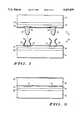
- FIG. 1is a simplified illustration of inter-substrate plug and receptacle interconnects-between first and second semiconductor chips;
- FIGS. 2-6illustrate a process of forming the inter-substrate receptacle interconnects of FIG. 1;
- FIGS. 7-11illustrate a process of forming the inter-substrate plug interconnects of FIG. 1.
- the present inventionrelates to a method of electrically and mechanically interconnecting two high density integrated circuits with plug and receptacle interconnects. While surfaces of a variety of types, and for a variety of purposes may be connected together, a preferred use of the present invention is for the electrical and mechanical interconnection of two integrated circuit chips, or for the connection of an integrated circuit chip to another substrate, e.g. alumina, for use in multi-chip modules or hybrid applications. The interconnections are separable and reusable.
- Semiconductor chip 10includes a semiconductor substrate 12 on which has been fabricated an integrated circuit (IC) device layer 14, an interconnect layer 16 and an isolation layer 20. Within interconnect layer 16 are conducting pads 18 which are connected to inter-substrate interconnect plugs 22.
- IC device layer 14 and interconnect layer 16are highly symbolic layers which in fact can be quite complex, and in many cases are not strictly restricted to layers as indicated, but may be interspersed with one another.
- IC device layer 14includes passive and active circuit elements formed using standard IC industry processing steps such ion implantation, thermal diffusion, wet and dry etching, physical and chemical deposition, and photolithographic techniques.
- Interconnect layer 16includes possibly complex configurations of conductors and dielectrics, possibly in multiple layers, which serve the function of interconnecting passive and active devices into circuits or sub-circuits.
- Pads 18are conducting locations that serve as a mechanical base for inter-substrate connecting plugs 22 and also serve to interconnect plugs 22 with other conductors in interconnect layer 16 which in turn connect with circuit elements in IC device layer 14.
- Isolation layer 20serves as passivation of the conducting layers in interconnect layer 16 and also functions as an etch differentiation layer during the fabrication process.
- second semiconductor chip 24includes semiconductor substrate 26, IC device layer 28, interconnect layer 30 and isolation layer 34.
- interconnect layer 30Within interconnect layer 30 are conducting pads 32 which are connected to inter-substrate interconnect receptacles 36.
- IC device layer 28includes passive and active circuit elements formed using standard IC industry processing steps.
- Interconnect layer 30includes possibly complex configurations of conductors and dielectrics, possibly in multiple layers, which serve the function of interconnecting passive and active devices into circuits or sub-circuits.
- Pads 32are conducting locations that serve as a mechanical base for inter-substrate connecting receptacles 36 and also serve to interconnect receptacles 36 with other conductors in interconnect layer 30 which in turn connect with circuit elements in IC device layer 28.
- Isolation layer 34serves as passivation of the conducting layers in interconnect layer 30 and also functions as an etch differentiation layer during the fabrication process.
- semiconductor chips 10 and 24are electrically and mechanically interconnected by aligning and inserting inter-substrate interconnect plugs 22 into inter-substrate interconnect receptacles 36.
- the sides of receptacles 36are flexible and elastic such that plugs 22 are gripped and retained by receptacles 36.
- This elastic, gripping actionserves multiple purposes; 1) it ensures that once semiconductor chip 10 is engaged with semiconductor chip 24, the two chips remain contacted unless forcible pulled apart; 2) it provides better electrical contact reliability by the sliding action of insertion which can puncture through thin oxides or surface contamination; and 3) once contact is made, the pressure due to the gripping action can serve to maintain a gas-tight seal to ensure long term reliability for electrical contact.
- receptacles 36may break, or be permanently distorted. Thus, it is necessary to select the proper combinations of material and geometrical properties to form plugs 22 and receptacles 36. For example, if the height of receptacles 36 is 4 ⁇ m, the thickness is 0.2 ⁇ m, and the material is polysilicon, calculations indicate that the opening of receptacles 36 could be expanded by 0.5 ⁇ m and the stress level within the material would be approximately one-tenth of the published yield, or fracture stress. At the same time, the gripping effect of hundreds or even thousands of receptacles 36, should provide very substantial mechanical retention.
- the insertion processshould be accomplished in very clean conditions and semiconductor chips 10 and 24 must be precisely positioned in order to achieve insertion.
- Robotic placement of two chips relative to one anothercan currently be achieved to an accuracy better than 1.0 ⁇ m, and this is sufficient for certain useful sizes of inter-chip interconnect plugs 22 and receptacles 36.
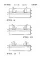
- FIGS. 2-6illustrate a process sequence suitable for fabrication of interconnect receptacles 36.
- semiconductor substrate 26is shown after completion of fabrication steps which have formed IC device layer 28, interconnect layer 30, conducting pads 32 and isolation layer 34.
- FIG. 2illustrates a dielectric layer 38 followed by photoresist layer 40.
- Dielectric layer 38is prepared in such a manner as to have an etch rate that is dependent on height above isolation layer 34 in order that in a subsequent step, see FIG. 4, an isotropic etch results in a predetermined wall shape.
- dielectric layer 38is a phosphosilicate glass (PSG) with a vertically varying concentration of P 2 O 5 .
- PSGphosphosilicate glass
- the etch rate of PSG in HFvaries dramatically with the P 2 O 5 concentration.
- the etch rate of 450° C.-deposited PSG in HFvaries from about 25 ⁇ /sec to 200 ⁇ /sec if the concentration of P 2 O 5 varies from 0 to 8 mole %.
- PSGis achieved by a chemical vapor deposition reaction using SiH 4 , PH 3 and O 2 and the resulting P 2 O 5 concentration may be controlled through control of the PH 3 concentration. By programming the concentration of PH 3 during deposition, the desired etch rate profile can be achieved. It should be clear, however, that other dielectric materials, etches and deposition variables may be utilized to achieve similar results.
- a maskis used to expose and develop photoresist 40 which opens the photoresist in locations where receptacles 36 of FIG. 1 are to be formed.
- An anisotropic reactive ion etching (RIE) processis then used to remove dielectric material 38 in vertical trenches of approximately 3-4 ⁇ m in depth as shown in FIG. 3.
- Isolation layer 34is chosen primarily as an etch-stop for a subsequent wet etch, but can also be used, together with laser interferometry, to provide an etch-rate signal during RIE to indicate when dielectric layer 38 has been etched through.
- pads 32can serve as an etch stop for the RIE etch.
- isolation layer 34is selected as Si 3 N 4 in the present embodiment
- the anisotropic etchis an RIE etch using halogen chemistries, such as CHF 3 +O 2
- pads 32are doped polysilicon.
- an HF etchis used to etch dielectric layer 38 in an isotropic manner, but with an etch rate dependent on the concentration of P 2 O 5 in dielectric layer 38, which varies as a function of height, resulting in a predetermined shaped region (cavity) 39 as shown.
- an additional etchsuch as phosphoric acid, is used to ensure that isolation layer 34 is cleared from the surface of pads 32.
- Conductive layer 37is conformally deposited to a predetermined thickness.
- Conductive layer 37is heavily doped polysilicon deposited to a thickness of around 0.2 ⁇ m.
- Use of low pressure CVD to deposit polysilicon conductive layer 37is known to allow highly conformal deposition even into extremely small openings, and will allow even smaller geometries.
- conductive layer 37is shown as a top view.
- the shaped regions 39 which are to become receptacle connectors 36 of FIG. 1are at this stage tub-like cavities with closed ends and joined together by conducting layer 37 on the surface.
- conducting layer 37In order to achieve the free-standing, receptacle-like configuration depicted in FIG. 1, conducting layer 37 must be etched to provide isolated receptacles 36. In order for the sides of receptacles 36 to be flexible, the ends of the tub-like regions of conducting layer 37 are opened for greater flexibility. These steps are accomplished through a sequence of photolithographic and etching steps, which are indicated by photolithographic patterns 42 and 43.
- a positive photoresistis applied to the surface, and pattern 42 is formed through exposure and development, which leaves photoresist within the region defined by pattern 42, and exposing the remaining surface of conductive layer 37.
- An anisotropic etch of conductive layer 37results in electrically isolated conductive regions, still surrounded by dielectric layer 38 of FIG. 5, and still of a tub-like configuration.
- dielectric layer 38 of FIG. 5is implemented to remove all of dielectric layer 38 down to isolation layer 24. Isolation layer 24 can serve as an end-point signal. This step exposes the ends of the conductive tub-like structures, but leaves the sides of the tub-like structures protected by photoresist on the inside, and dielectric layer 38 on the outside. Some isotropic etching of dielectric 38 may be necessary to adequately expose the ends of the tubs. Consequently, an isotropic etch of conductive layer 37 for a predetermined time, opens the ends of the tub-like structures.
- a strip of the photoresist, and an isotropic etch of dielectric layer 38completely removes all remaining dielectric material 38, resulting in the free-standing receptacles 36 as shown in FIG. 1.
- the ends of tub-like regions of conducting layer 37may be left closed for certain combinations of plug and receptacle geometries which provide sufficient flexibility without opening the ends of the tub-like structures.
- the anisotropic etch for dielectric layer 38is an RIE etch using halogen chemistry, e.g. CHF 3 +O 2 .
- the polysilicon etch for dielectric layer 37is an isotropic silicon etch having high selectivity with respect to dielectric layers 38 and 34.
- the isotropic etch for dielectric layer 38is HF which has a high selectivity against polysilicon layer 37 and Si 3 N 4 isolating layer 24.
- Alternative etch sequences, and etch chemistriesmay also be considered, depending on the materials used for conducting layer 37, isolating layer 24 and dielectric layer 38. With the proper combination of materials and etch chemistries, a single anisotropic etch using pattern 42 achieves the same results as the foregoing, more complex procedure.
- FIGS. 7-11depict a process for fabricating plugs 22 of FIG. 1.
- substrate 12has already undergone conventional processing resulting in IC device layer 14, interconnect layer 16, isolation layer 20 and conducting pads 18.
- Dielectric layer 44is deposited with a predetermined variation of composition so as to achieve an etch rate that varies with height above isolation layer 20.
- phosphosilicate glass (PSG)with a variation of P 2 O 5 content gives such properties when etched with HF.
- Photoresist layer 46is then deposited on dielectric layer 44.
- photoresist layer 46is patterned to define locations for interconnect plugs 22 of FIG. 1 and a combination of an anisotropic etch followed by an isotropic etch, as described for FIGS. 3 and 4, results in the shaped regions 50 of FIG. 9. Photoresist layer 46 is removed.
- interconnect plugs 22have been formed by a selective deposition process, which nucleates at the surface of pads 18 and fills the cavity of regions 50 with a conductive material.
- pads 18are heavily doped polysilicon
- plug-like members 22are also heavily doped polysilicon, which can be selectively deposited using CVD of SiH 4 +H 2 .
- other conductive materials and methodsmay be considered, e.g. selective deposition of tungsten, or plating of copper, nickel or other conductors.
- dielectric layer 44is removed by an isotropic etch such as HF which has high selectivity against polysilicon and Si 3 N 4 leaving plugs 22 protruding from semiconductor chip 10 like that shown in FIG. 1.
- isotropic etchsuch as HF which has high selectivity against polysilicon and Si 3 N 4 leaving plugs 22 protruding from semiconductor chip 10 like that shown in FIG. 1.
- interconnect plug 22 and receptacles 36are just one embodiment of the invention.
- Some other variations which have been consideredare the use of a plug 22 with a shape which interlocks with receptacle 36, thereby giving increased retention, and a tendency to draw one surface towards the other.
- Other variationsinclude the use of additional plated layers on the surfaces of connecting members 22 and 36 such that in final assembly, a short heat treatment causes the two surfaces to be fused together in a more permanent fashion.
- Pb-Sn alloysare used for this purpose due to their low temperature melting point, and well-known properties.
- Other uses for the connection technology described here, besides connecting two integrated circuit chips,can also be identified.
- One further exampleis a heat dissipation substrate which is attached to active devices and dissipate heat.
- Micro packagesmay be built which mount on micro pins on circuit boards. Any application where it is beneficial to attach one surface to another in predetermined locations, and at high resolution, may benefit from this invention.
Landscapes
- Engineering & Computer Science (AREA)
- Microelectronics & Electronic Packaging (AREA)
- Power Engineering (AREA)
- Computer Hardware Design (AREA)
- Physics & Mathematics (AREA)
- Condensed Matter Physics & Semiconductors (AREA)
- General Physics & Mathematics (AREA)
- Manufacturing & Machinery (AREA)
- Internal Circuitry In Semiconductor Integrated Circuit Devices (AREA)
Abstract
Description
Claims (17)
Priority Applications (1)
| Application Number | Priority Date | Filing Date | Title |
|---|---|---|---|
| US08/177,024US5457879A (en) | 1994-01-04 | 1994-01-04 | Method of shaping inter-substrate plug and receptacles interconnects |
Applications Claiming Priority (1)
| Application Number | Priority Date | Filing Date | Title |
|---|---|---|---|
| US08/177,024US5457879A (en) | 1994-01-04 | 1994-01-04 | Method of shaping inter-substrate plug and receptacles interconnects |
Publications (1)
| Publication Number | Publication Date |
|---|---|
| US5457879Atrue US5457879A (en) | 1995-10-17 |
Family
ID=22646869
Family Applications (1)
| Application Number | Title | Priority Date | Filing Date |
|---|---|---|---|
| US08/177,024Expired - Fee RelatedUS5457879A (en) | 1994-01-04 | 1994-01-04 | Method of shaping inter-substrate plug and receptacles interconnects |
Country Status (1)
| Country | Link |
|---|---|
| US (1) | US5457879A (en) |
Cited By (36)
| Publication number | Priority date | Publication date | Assignee | Title |
|---|---|---|---|---|
| DE19612839A1 (en)* | 1996-02-06 | 1997-08-07 | Asea Brown Boveri | Power semiconductor module |
| US5915167A (en)* | 1997-04-04 | 1999-06-22 | Elm Technology Corporation | Three dimensional structure memory |
| US5985693A (en)* | 1994-09-30 | 1999-11-16 | Elm Technology Corporation | High density three-dimensional IC interconnection |
| US6150192A (en)* | 1998-04-28 | 2000-11-21 | Trw Inc. | Apparatus and method for snap-on thermo-compression bonding |
| WO2000079590A1 (en)* | 1999-06-17 | 2000-12-28 | Infineon Technologies Ag | Electronic device with flexible contacting points |
| US6208027B1 (en)* | 1999-03-10 | 2001-03-27 | Advanced Micro Devices, Inc. | Temporary interconnect for semiconductor devices |
| US6303991B1 (en)* | 1999-05-27 | 2001-10-16 | Fci Americas Technology, Inc. | Electronic package and contact therefor |
| US6320254B1 (en)* | 1999-02-04 | 2001-11-20 | United Microelectronics Corp. | Plug structure |
| US6551857B2 (en) | 1997-04-04 | 2003-04-22 | Elm Technology Corporation | Three dimensional structure integrated circuits |
| US20030107119A1 (en)* | 2001-12-06 | 2003-06-12 | Samsung Electronics Co., Ltd. | Multi-chip package (MCP) with a conductive bar and method for manufacturing the same |
| US6612023B1 (en)* | 1996-09-06 | 2003-09-02 | Hewlett-Packard Development Company, L.P. | Method for registering a component lead with a U-shaped metalized pad |
| US6682981B2 (en) | 1992-04-08 | 2004-01-27 | Elm Technology Corporation | Stress controlled dielectric integrated circuit fabrication |
| US20040094846A1 (en)* | 2002-08-21 | 2004-05-20 | Kazuyuki Yamada | Semiconductor device mounting method, semiconductor device mounting structure, ellectro-optical device, electro-optical device manufacturing method and electronic device |
| US20050156308A1 (en)* | 2004-01-21 | 2005-07-21 | Anton Legen | Connecting elements on semiconductor chips for semiconductor components and methods for producing the same |
| US20060055043A1 (en)* | 2004-09-13 | 2006-03-16 | Taiwan Semiconductor Manufacturing Company, Ltd. | Connection structure for semiconductor devices |
| US7176545B2 (en) | 1992-04-08 | 2007-02-13 | Elm Technology Corporation | Apparatus and methods for maskless pattern generation |
| US20070166978A1 (en)* | 2004-02-25 | 2007-07-19 | Jean Brun | Microelectronic interconnect device comprising localised conductive pins |
| US7302982B2 (en) | 2001-04-11 | 2007-12-04 | Avery Dennison Corporation | Label applicator and system |
| US7402897B2 (en) | 2002-08-08 | 2008-07-22 | Elm Technology Corporation | Vertical system integration |
| US20110079916A1 (en)* | 2009-10-02 | 2011-04-07 | Texas Instruments Incorporated | Electronic assemblies including mechanically secured protruding bonding conductor joints |
| US20120104076A1 (en)* | 2004-01-22 | 2012-05-03 | Tadatomo Suga | Joining method and device produced by this method and joining unit |
| WO2012059659A1 (en)* | 2010-11-05 | 2012-05-10 | Commissariat A L'energie Atomique Et Aux Energies Alternatives | Connecting elements for producing hybrid electronic circuits |
| US20120292763A1 (en)* | 2010-02-09 | 2012-11-22 | International Business Machines Corporation | Electromigration immune through-substrate vias |
| US20140145329A1 (en)* | 2003-10-06 | 2014-05-29 | Tessera, Inc. | Fine pitch microcontacts and method for forming thereof |
| US20150236248A1 (en)* | 2014-02-18 | 2015-08-20 | Everspin Technologies, Inc. | Top electrode etch in a magnetoresistive device and devices manufactured using same |
| US9397063B2 (en) | 2010-07-27 | 2016-07-19 | Tessera, Inc. | Microelectronic packages with nanoparticle joining |
| US9466788B2 (en) | 2014-02-18 | 2016-10-11 | Everspin Technologies, Inc. | Top electrode etch in a magnetoresistive device and devices manufactured using same |
| US9496236B2 (en) | 2010-12-10 | 2016-11-15 | Tessera, Inc. | Interconnect structure |
| US9633971B2 (en) | 2015-07-10 | 2017-04-25 | Invensas Corporation | Structures and methods for low temperature bonding using nanoparticles |
| US20180233485A1 (en)* | 2017-02-14 | 2018-08-16 | Nanya Technology Corporation | Semiconductor structure and manufacturing method thereof |
| US10535626B2 (en) | 2015-07-10 | 2020-01-14 | Invensas Corporation | Structures and methods for low temperature bonding using nanoparticles |
| US20200118881A1 (en)* | 2018-10-11 | 2020-04-16 | International Business Machines Corporation | Self-aligned fin recesses in nanosheet field effect transistors |
| CN113133327A (en)* | 2019-10-31 | 2021-07-16 | 京东方科技集团股份有限公司 | Bearing back plate, preparation method thereof and back plate |
| US11973056B2 (en) | 2016-10-27 | 2024-04-30 | Adeia Semiconductor Technologies Llc | Methods for low temperature bonding using nanoparticles |
| WO2024108432A1 (en)* | 2022-11-23 | 2024-05-30 | 厦门市芯颖显示科技有限公司 | Micro bonding device, bonding backplane and display device |
| US12211809B2 (en) | 2020-12-30 | 2025-01-28 | Adeia Semiconductor Bonding Technologies Inc. | Structure with conductive feature and method of forming same |
Citations (5)
| Publication number | Priority date | Publication date | Assignee | Title |
|---|---|---|---|---|
| US4612554A (en)* | 1985-07-29 | 1986-09-16 | Xerox Corporation | High density thermal ink jet printhead |
| US4952272A (en)* | 1988-05-30 | 1990-08-28 | Hitachi, Ltd. | Method of manufacturing probing head for testing equipment of semi-conductor large scale integrated circuits |
| US4963511A (en)* | 1987-11-30 | 1990-10-16 | Texas Instruments Incorporated | Method of reducing tungsten selectivity to a contact sidewall |
| US4991285A (en)* | 1989-11-17 | 1991-02-12 | Rockwell International Corporation | Method of fabricating multi-layer board |
| US5108541A (en)* | 1991-03-06 | 1992-04-28 | International Business Machines Corp. | Processes for electrically conductive decals filled with inorganic insulator material |
- 1994
- 1994-01-04USUS08/177,024patent/US5457879A/ennot_activeExpired - Fee Related
Patent Citations (5)
| Publication number | Priority date | Publication date | Assignee | Title |
|---|---|---|---|---|
| US4612554A (en)* | 1985-07-29 | 1986-09-16 | Xerox Corporation | High density thermal ink jet printhead |
| US4963511A (en)* | 1987-11-30 | 1990-10-16 | Texas Instruments Incorporated | Method of reducing tungsten selectivity to a contact sidewall |
| US4952272A (en)* | 1988-05-30 | 1990-08-28 | Hitachi, Ltd. | Method of manufacturing probing head for testing equipment of semi-conductor large scale integrated circuits |
| US4991285A (en)* | 1989-11-17 | 1991-02-12 | Rockwell International Corporation | Method of fabricating multi-layer board |
| US5108541A (en)* | 1991-03-06 | 1992-04-28 | International Business Machines Corp. | Processes for electrically conductive decals filled with inorganic insulator material |
Cited By (103)
| Publication number | Priority date | Publication date | Assignee | Title |
|---|---|---|---|---|
| US7485571B2 (en) | 1992-04-08 | 2009-02-03 | Elm Technology Corporation | Method of making an integrated circuit |
| US7307020B2 (en) | 1992-04-08 | 2007-12-11 | Elm Technology Corporation | Membrane 3D IC fabrication |
| US6713327B2 (en) | 1992-04-08 | 2004-03-30 | Elm Technology Corporation | Stress controlled dielectric integrated circuit fabrication |
| US6682981B2 (en) | 1992-04-08 | 2004-01-27 | Elm Technology Corporation | Stress controlled dielectric integrated circuit fabrication |
| US7911012B2 (en) | 1992-04-08 | 2011-03-22 | Taiwan Semiconductor Manufacturing Co., Ltd. | Flexible and elastic dielectric integrated circuit |
| US7820469B2 (en) | 1992-04-08 | 2010-10-26 | Taiwan Semiconductor Manufacturing Co., Ltd. | Stress-controlled dielectric integrated circuit |
| US7763948B2 (en) | 1992-04-08 | 2010-07-27 | Taiwan Semiconductor Manufacturing Co., Ltd. | Flexible and elastic dielectric integrated circuit |
| US7670893B2 (en) | 1992-04-08 | 2010-03-02 | Taiwan Semiconductor Manufacturing Co., Ltd. | Membrane IC fabrication |
| US7550805B2 (en) | 1992-04-08 | 2009-06-23 | Elm Technology Corporation | Stress-controlled dielectric integrated circuit |
| US7176545B2 (en) | 1992-04-08 | 2007-02-13 | Elm Technology Corporation | Apparatus and methods for maskless pattern generation |
| US7385835B2 (en) | 1992-04-08 | 2008-06-10 | Elm Technology Corporation | Membrane 3D IC fabrication |
| US7479694B2 (en) | 1992-04-08 | 2009-01-20 | Elm Technology Corporation | Membrane 3D IC fabrication |
| US6765279B2 (en) | 1992-04-08 | 2004-07-20 | Elm Technology Corporation | Membrane 3D IC fabrication |
| US7615837B2 (en) | 1992-04-08 | 2009-11-10 | Taiwan Semiconductor Manufacturing Company | Lithography device for semiconductor circuit pattern generation |
| US7242012B2 (en) | 1992-04-08 | 2007-07-10 | Elm Technology Corporation | Lithography device for semiconductor circuit pattern generator |
| US7223696B2 (en) | 1992-04-08 | 2007-05-29 | Elm Technology Corporation | Methods for maskless lithography |
| US5985693A (en)* | 1994-09-30 | 1999-11-16 | Elm Technology Corporation | High density three-dimensional IC interconnection |
| US5777849A (en)* | 1996-02-06 | 1998-07-07 | Asea Brown Boveri Ag | Power semiconductor module having elongate plug contacts |
| DE19612839A1 (en)* | 1996-02-06 | 1997-08-07 | Asea Brown Boveri | Power semiconductor module |
| US6612023B1 (en)* | 1996-09-06 | 2003-09-02 | Hewlett-Packard Development Company, L.P. | Method for registering a component lead with a U-shaped metalized pad |
| US8928119B2 (en) | 1997-04-04 | 2015-01-06 | Glenn J. Leedy | Three dimensional structure memory |
| US8791581B2 (en) | 1997-04-04 | 2014-07-29 | Glenn J Leedy | Three dimensional structure memory |
| US8318538B2 (en) | 1997-04-04 | 2012-11-27 | Elm Technology Corp. | Three dimensional structure memory |
| US9401183B2 (en) | 1997-04-04 | 2016-07-26 | Glenn J. Leedy | Stacked integrated memory device |
| US8410617B2 (en) | 1997-04-04 | 2013-04-02 | Elm Technology | Three dimensional structure memory |
| US9087556B2 (en) | 1997-04-04 | 2015-07-21 | Glenn J Leedy | Three dimension structure memory |
| US7138295B2 (en) | 1997-04-04 | 2006-11-21 | Elm Technology Corporation | Method of information processing using three dimensional integrated circuits |
| US6632706B1 (en) | 1997-04-04 | 2003-10-14 | Elm Technology Corporation | Three dimensional structure integrated circuit fabrication process |
| US8933570B2 (en) | 1997-04-04 | 2015-01-13 | Elm Technology Corp. | Three dimensional structure memory |
| US7193239B2 (en) | 1997-04-04 | 2007-03-20 | Elm Technology Corporation | Three dimensional structure integrated circuit |
| US8035233B2 (en)* | 1997-04-04 | 2011-10-11 | Elm Technology Corporation | Adjacent substantially flexible substrates having integrated circuits that are bonded together by non-polymeric layer |
| US6563224B2 (en) | 1997-04-04 | 2003-05-13 | Elm Technology Corporation | Three dimensional structure integrated circuit |
| US5915167A (en)* | 1997-04-04 | 1999-06-22 | Elm Technology Corporation | Three dimensional structure memory |
| US8907499B2 (en) | 1997-04-04 | 2014-12-09 | Glenn J Leedy | Three dimensional structure memory |
| US8629542B2 (en) | 1997-04-04 | 2014-01-14 | Glenn J. Leedy | Three dimensional structure memory |
| US6133640A (en)* | 1997-04-04 | 2000-10-17 | Elm Technology Corporation | Three-dimensional structure memory |
| US6551857B2 (en) | 1997-04-04 | 2003-04-22 | Elm Technology Corporation | Three dimensional structure integrated circuits |
| US8841778B2 (en) | 1997-04-04 | 2014-09-23 | Glenn J Leedy | Three dimensional memory structure |
| US8824159B2 (en) | 1997-04-04 | 2014-09-02 | Glenn J. Leedy | Three dimensional structure memory |
| US7474004B2 (en) | 1997-04-04 | 2009-01-06 | Elm Technology Corporation | Three dimensional structure memory |
| US7705466B2 (en) | 1997-04-04 | 2010-04-27 | Elm Technology Corporation | Three dimensional multi layer memory and control logic integrated circuit structure |
| US8288206B2 (en) | 1997-04-04 | 2012-10-16 | Elm Technology Corp | Three dimensional structure memory |
| US7504732B2 (en) | 1997-04-04 | 2009-03-17 | Elm Technology Corporation | Three dimensional structure memory |
| US6208545B1 (en) | 1997-04-04 | 2001-03-27 | Glenn J. Leedy | Three dimensional structure memory |
| US8796862B2 (en) | 1997-04-04 | 2014-08-05 | Glenn J Leedy | Three dimensional memory structure |
| US6172414B1 (en)* | 1998-04-28 | 2001-01-09 | Trw Inc. | Apparatus and method for snap-on thermo-compression bonding |
| US6150192A (en)* | 1998-04-28 | 2000-11-21 | Trw Inc. | Apparatus and method for snap-on thermo-compression bonding |
| US6320254B1 (en)* | 1999-02-04 | 2001-11-20 | United Microelectronics Corp. | Plug structure |
| US6208027B1 (en)* | 1999-03-10 | 2001-03-27 | Advanced Micro Devices, Inc. | Temporary interconnect for semiconductor devices |
| US6303991B1 (en)* | 1999-05-27 | 2001-10-16 | Fci Americas Technology, Inc. | Electronic package and contact therefor |
| WO2000079590A1 (en)* | 1999-06-17 | 2000-12-28 | Infineon Technologies Ag | Electronic device with flexible contacting points |
| US6555415B2 (en) | 1999-06-17 | 2003-04-29 | Infineon Technologies Ag | Electronic configuration with flexible bonding pads |
| US7302982B2 (en) | 2001-04-11 | 2007-12-04 | Avery Dennison Corporation | Label applicator and system |
| US7531890B2 (en) | 2001-12-06 | 2009-05-12 | Samsung Electronics Co., Ltd. | Multi-chip package (MCP) with a conductive bar and method for manufacturing the same |
| US20030107119A1 (en)* | 2001-12-06 | 2003-06-12 | Samsung Electronics Co., Ltd. | Multi-chip package (MCP) with a conductive bar and method for manufacturing the same |
| US20050205968A1 (en)* | 2001-12-06 | 2005-09-22 | Samsung Electronics Co., Ltd. | Multi-chip package (MCP) with a conductive bar and method for manufacturing the same |
| US6908785B2 (en)* | 2001-12-06 | 2005-06-21 | Samsung Electronics Co., Ltd. | Multi-chip package (MCP) with a conductive bar and method for manufacturing the same |
| US8269327B2 (en) | 2002-08-08 | 2012-09-18 | Glenn J Leedy | Vertical system integration |
| US8587102B2 (en) | 2002-08-08 | 2013-11-19 | Glenn J Leedy | Vertical system integration |
| US7402897B2 (en) | 2002-08-08 | 2008-07-22 | Elm Technology Corporation | Vertical system integration |
| US8080442B2 (en) | 2002-08-08 | 2011-12-20 | Elm Technology Corporation | Vertical system integration |
| US20040094846A1 (en)* | 2002-08-21 | 2004-05-20 | Kazuyuki Yamada | Semiconductor device mounting method, semiconductor device mounting structure, ellectro-optical device, electro-optical device manufacturing method and electronic device |
| US7180196B2 (en)* | 2002-08-21 | 2007-02-20 | Seiko Epson Corporation | Semiconductor device mounting method, semiconductor device mounting structure, electro-optical device, electro-optical device manufacturing method and electronic device |
| US20140145329A1 (en)* | 2003-10-06 | 2014-05-29 | Tessera, Inc. | Fine pitch microcontacts and method for forming thereof |
| US20050156308A1 (en)* | 2004-01-21 | 2005-07-21 | Anton Legen | Connecting elements on semiconductor chips for semiconductor components and methods for producing the same |
| US7253514B2 (en)* | 2004-01-21 | 2007-08-07 | Infineon Technologies, Ag | Self-supporting connecting element for a semiconductor chip |
| US20120104076A1 (en)* | 2004-01-22 | 2012-05-03 | Tadatomo Suga | Joining method and device produced by this method and joining unit |
| US8651363B2 (en)* | 2004-01-22 | 2014-02-18 | Bondtech, Inc. | Joining method and device produced by this method and joining unit |
| US7563703B2 (en)* | 2004-02-25 | 2009-07-21 | Commissariat A L'energie Atomique | Microelectronic interconnect device comprising localised conductive pins |
| US20070166978A1 (en)* | 2004-02-25 | 2007-07-19 | Jean Brun | Microelectronic interconnect device comprising localised conductive pins |
| US7705464B2 (en)* | 2004-09-13 | 2010-04-27 | Taiwan Semiconductor Manufacturing Company, Ltd. | Connection structure for semiconductor devices |
| US20060055043A1 (en)* | 2004-09-13 | 2006-03-16 | Taiwan Semiconductor Manufacturing Company, Ltd. | Connection structure for semiconductor devices |
| CN100394594C (en)* | 2004-09-13 | 2008-06-11 | 台湾积体电路制造股份有限公司 | Semiconductor element and connection structure of semiconductor element |
| US20110079916A1 (en)* | 2009-10-02 | 2011-04-07 | Texas Instruments Incorporated | Electronic assemblies including mechanically secured protruding bonding conductor joints |
| US8143704B2 (en)* | 2009-10-02 | 2012-03-27 | Texas Instruments Incorporated | Electronic assemblies including mechanically secured protruding bonding conductor joints |
| US8859414B2 (en)* | 2009-10-02 | 2014-10-14 | Texas Instruments Incorporated | Electronic assemblies including mechanically secured protruding bonding conductor joints |
| US20120149155A1 (en)* | 2009-10-02 | 2012-06-14 | Texas Instruments Incorporated | Electronic Assemblies Including Mechanically Secured Protruding Bonding Conductor Joints |
| US9153558B2 (en)* | 2010-02-09 | 2015-10-06 | International Business Machines Corporation | Electromigration immune through-substrate vias |
| US20120292763A1 (en)* | 2010-02-09 | 2012-11-22 | International Business Machines Corporation | Electromigration immune through-substrate vias |
| US9397063B2 (en) | 2010-07-27 | 2016-07-19 | Tessera, Inc. | Microelectronic packages with nanoparticle joining |
| WO2012059659A1 (en)* | 2010-11-05 | 2012-05-10 | Commissariat A L'energie Atomique Et Aux Energies Alternatives | Connecting elements for producing hybrid electronic circuits |
| US9166338B2 (en) | 2010-11-05 | 2015-10-20 | Commissariat A L 'energie Atomique Et Aux Energies Alternatives | Connecting elements for producing hybrid electronic circuits |
| FR2967296A1 (en)* | 2010-11-05 | 2012-05-11 | Commissariat Energie Atomique | CONNECTION ELEMENTS FOR HYBRIDIZATION OF ELECTRONIC CIRCUITS |
| US9496236B2 (en) | 2010-12-10 | 2016-11-15 | Tessera, Inc. | Interconnect structure |
| US20150236248A1 (en)* | 2014-02-18 | 2015-08-20 | Everspin Technologies, Inc. | Top electrode etch in a magnetoresistive device and devices manufactured using same |
| US9466788B2 (en) | 2014-02-18 | 2016-10-11 | Everspin Technologies, Inc. | Top electrode etch in a magnetoresistive device and devices manufactured using same |
| US9595665B2 (en) | 2014-02-18 | 2017-03-14 | Everspin Technologies, Inc. | Non-reactive photoresist removal and spacer layer optimization in a magnetoresistive device |
| US10535626B2 (en) | 2015-07-10 | 2020-01-14 | Invensas Corporation | Structures and methods for low temperature bonding using nanoparticles |
| US11710718B2 (en) | 2015-07-10 | 2023-07-25 | Adeia Semiconductor Technologies Llc | Structures and methods for low temperature bonding using nanoparticles |
| US9633971B2 (en) | 2015-07-10 | 2017-04-25 | Invensas Corporation | Structures and methods for low temperature bonding using nanoparticles |
| US10886250B2 (en) | 2015-07-10 | 2021-01-05 | Invensas Corporation | Structures and methods for low temperature bonding using nanoparticles |
| US10892246B2 (en) | 2015-07-10 | 2021-01-12 | Invensas Corporation | Structures and methods for low temperature bonding using nanoparticles |
| US9818713B2 (en) | 2015-07-10 | 2017-11-14 | Invensas Corporation | Structures and methods for low temperature bonding using nanoparticles |
| US12027487B2 (en) | 2016-10-27 | 2024-07-02 | Adeia Semiconductor Technologies Llc | Structures for low temperature bonding using nanoparticles |
| US11973056B2 (en) | 2016-10-27 | 2024-04-30 | Adeia Semiconductor Technologies Llc | Methods for low temperature bonding using nanoparticles |
| US20180233485A1 (en)* | 2017-02-14 | 2018-08-16 | Nanya Technology Corporation | Semiconductor structure and manufacturing method thereof |
| US10957601B2 (en)* | 2018-10-11 | 2021-03-23 | International Business Machines Corporation | Self-aligned fin recesses in nanosheet field effect transistors |
| US20200118881A1 (en)* | 2018-10-11 | 2020-04-16 | International Business Machines Corporation | Self-aligned fin recesses in nanosheet field effect transistors |
| CN113133327B (en)* | 2019-10-31 | 2024-01-26 | 京东方科技集团股份有限公司 | Undertake back plate and preparation method thereof, back plate |
| CN113133327A (en)* | 2019-10-31 | 2021-07-16 | 京东方科技集团股份有限公司 | Bearing back plate, preparation method thereof and back plate |
| US12087892B2 (en) | 2019-10-31 | 2024-09-10 | Boe Technology Group Co., Ltd. | Supporting backplane, manufacturing method therefor and backplane |
| US12211809B2 (en) | 2020-12-30 | 2025-01-28 | Adeia Semiconductor Bonding Technologies Inc. | Structure with conductive feature and method of forming same |
| WO2024108432A1 (en)* | 2022-11-23 | 2024-05-30 | 厦门市芯颖显示科技有限公司 | Micro bonding device, bonding backplane and display device |
Similar Documents
| Publication | Publication Date | Title |
|---|---|---|
| US5457879A (en) | Method of shaping inter-substrate plug and receptacles interconnects | |
| US5424245A (en) | Method of forming vias through two-sided substrate | |
| US6114221A (en) | Method and apparatus for interconnecting multiple circuit chips | |
| US6509623B2 (en) | Microelectronic air-gap structures and methods of forming the same | |
| US6271059B1 (en) | Chip interconnection structure using stub terminals | |
| US4987099A (en) | Method for selectively filling contacts or vias or various depths with CVD tungsten | |
| US6420209B1 (en) | Integrated circuits and methods for their fabrication | |
| US5998292A (en) | Method for making three dimensional circuit integration | |
| US5767001A (en) | Process for producing semiconductor components between which contact is made vertically | |
| US5646067A (en) | Method of bonding wafers having vias including conductive material | |
| US5618752A (en) | Method of fabrication of surface mountable integrated circuits | |
| US6593644B2 (en) | System of a package fabricated on a semiconductor or dielectric wafer with wiring on one face, vias extending through the wafer, and external connections on the opposing face | |
| US5903045A (en) | Self-aligned connector for stacked chip module | |
| US5668409A (en) | Integrated circuit with edge connections and method | |
| CN101091243A (en) | Method and apparatus for single mask via | |
| KR20000070443A (en) | Semiconductor wafer fabrication of inside-wrapped contacts for electronic devices | |
| KR20050065684A (en) | Wafer passivation structure | |
| EP0307671A2 (en) | Method of making an electrically programmable integrated circuit with meltable contact bridges | |
| EP0926726A1 (en) | Fabrication process and electronic device having front-back through contacts for bonding onto boards | |
| US20020135069A1 (en) | Electroplating methods for fabricating microelectronic interconnects | |
| KR100787371B1 (en) | Method for producing electrode and semiconductor device | |
| CN108511415A (en) | Electronic assembly manufacturing method | |
| KR0137978B1 (en) | Fabrication method of semiconductor device | |
| EP0306890A1 (en) | A semiconductor module having active devices disposed in substrate cavities | |
| JPS62261156A (en) | Method of forming conductive via route |
Legal Events
| Date | Code | Title | Description |
|---|---|---|---|
| AS | Assignment | Owner name:MOTOROLA, INC., ILLINOIS Free format text:ASSIGNMENT OF ASSIGNORS INTEREST;ASSIGNORS:GURTLER, RICHARD W.;HUGHES, HENRY G.;REEL/FRAME:006837/0310 Effective date:19931129 | |
| REMI | Maintenance fee reminder mailed | ||
| FPAY | Fee payment | Year of fee payment:4 | |
| SULP | Surcharge for late payment | ||
| FPAY | Fee payment | Year of fee payment:8 | |
| AS | Assignment | Owner name:FREESCALE SEMICONDUCTOR, INC., TEXAS Free format text:ASSIGNMENT OF ASSIGNORS INTEREST;ASSIGNOR:MOTOROLA, INC.;REEL/FRAME:015698/0657 Effective date:20040404 Owner name:FREESCALE SEMICONDUCTOR, INC.,TEXAS Free format text:ASSIGNMENT OF ASSIGNORS INTEREST;ASSIGNOR:MOTOROLA, INC.;REEL/FRAME:015698/0657 Effective date:20040404 | |
| AS | Assignment | Owner name:CITIBANK, N.A. AS COLLATERAL AGENT, NEW YORK Free format text:SECURITY AGREEMENT;ASSIGNORS:FREESCALE SEMICONDUCTOR, INC.;FREESCALE ACQUISITION CORPORATION;FREESCALE ACQUISITION HOLDINGS CORP.;AND OTHERS;REEL/FRAME:018855/0129 Effective date:20061201 Owner name:CITIBANK, N.A. AS COLLATERAL AGENT,NEW YORK Free format text:SECURITY AGREEMENT;ASSIGNORS:FREESCALE SEMICONDUCTOR, INC.;FREESCALE ACQUISITION CORPORATION;FREESCALE ACQUISITION HOLDINGS CORP.;AND OTHERS;REEL/FRAME:018855/0129 Effective date:20061201 | |
| REMI | Maintenance fee reminder mailed | ||
| LAPS | Lapse for failure to pay maintenance fees | ||
| STCH | Information on status: patent discontinuation | Free format text:PATENT EXPIRED DUE TO NONPAYMENT OF MAINTENANCE FEES UNDER 37 CFR 1.362 | |
| FP | Lapsed due to failure to pay maintenance fee | Effective date:20071017 | |
| AS | Assignment | Owner name:FREESCALE SEMICONDUCTOR, INC., TEXAS Free format text:PATENT RELEASE;ASSIGNOR:CITIBANK, N.A., AS COLLATERAL AGENT;REEL/FRAME:037354/0225 Effective date:20151207 |