US5457717A - Apparatus and method for eliminating mapping jitter - Google Patents
Apparatus and method for eliminating mapping jitterDownload PDFInfo
- Publication number
- US5457717A US5457717AUS08/158,967US15896793AUS5457717AUS 5457717 AUS5457717 AUS 5457717AUS 15896793 AUS15896793 AUS 15896793AUS 5457717 AUS5457717 AUS 5457717A
- Authority
- US
- United States
- Prior art keywords
- circuit
- value
- elastic
- asynchronous data
- gapfill
- Prior art date
- Legal status (The legal status is an assumption and is not a legal conclusion. Google has not performed a legal analysis and makes no representation as to the accuracy of the status listed.)
- Expired - Lifetime
Links
Images

Classifications
- H—ELECTRICITY
- H04—ELECTRIC COMMUNICATION TECHNIQUE
- H04J—MULTIPLEX COMMUNICATION
- H04J3/00—Time-division multiplex systems
- H04J3/02—Details
- H04J3/06—Synchronising arrangements
- H04J3/07—Synchronising arrangements using pulse stuffing for systems with different or fluctuating information rates or bit rates
- H04J3/076—Bit and byte stuffing, e.g. SDH/PDH desynchronisers, bit-leaking
Definitions
- the present inventionrelates in general to telecommunications networks and more particularly to an apparatus and method for eliminating mapping jitter.
- a desynchronizeris a device that recovers an embedded signal containing asynchronous data at a specific clock rate from within a higher rate digital bit stream of a synchronous channel.
- the clock rate for the embedded signalis unrelated to the clock rate for the synchronous channel.
- the embedded signalis multiplexed into the synchronous channel, it is necessary to synchronize the embedded signal with bit or byte timing adjustments.
- the process of recovering the asynchronous data and clock rate of the embedded signalis complicated by data gaps and overhead timing adjustments necessary to map the embedded signal into the synchronous channel.
- the conventional approach to accommodating the overhead gapsis to allow them to appear as fluctuations in the instantaneous fill level of a data buffer referred to as an elastic store.
- Clock recoveryis accomplished by using the fill level of the elastic store to drive a low pass filter, which in turn drives a voltage control oscillator, to produce a desired clock signal for synchronous transmission of the data from the elastic store.
- High frequency instantaneous variations in the elastic store fill valuedue to the overhead gaps installed during synchronization, are filtered by the low pass filter but not completely eliminated. Mapping jitter remains on the output of the desynchronizer due to instantaneous variations in the elastic store fill value that are not fully filtered out. Therefore, it is desirable to have a desynchronizer without any mapping jitter on its output.
- an apparatus and method for eliminating mapping jitterare provided which substantially eliminate or reduce disadvantages and problems associated with conventional desynchronizer devices.
- an apparatus for eliminating mapping jitterthat includes a demapper circuit for reading asynchronous data and a clock rate of an embedded signal within a synchronous payload envelope received over a synchronous channel and an elastic store circuit for storing the asynchronous data, including overhead gaps and timing adjustments, read by the demapper circuit according to the clock rate of the embedded signal.
- Instantaneous variations due to overhead gaps in a fill value of the elastic store circuitare determined by an overhead gapfill circuit.
- a mapping jitter elimination circuiteliminates the instantaneous variations determined by the overhead gapfill circuit in order to recover an output clock rate for the synchronous transfer of asynchronous data from the elastic store circuit.
- the apparatus and method of the present inventionprovide various technical advantages over conventional desynchronizer devices. For example, one technical advantage is in determining the instantaneous variations in the fill value of the elastic store circuit due to overhead gaps placed in the embedded signal during synchronization. Another technical advantage is in eliminating the instantaneous variations in order to recover an output clock rate for the synchronous transmission of the asynchronous data within the elastic store circuit. Yet another technical advantage is in eliminating mapping jitter from the recovered output clock rate of the desynchronizer device. Other technical advantages are readily apparent to one skilled in the art from the following figures, descriptions, and claims.
- FIG. 1illustrates a block diagram of a desynchronizer device
- FIG. 2illustrates a diagram of an embedded signal mapped into a synchronous payload envelope
- FIG. 3is a timing diagram illustrating an enhanced operating mode of the desynchronizer device.
- FIG. 4is a simplified schematic diagram of a low pass filter within the desynchronizer device.
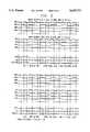
- FIG. 1is a block diagram of a desynchronizer device 10.
- Desynchronizer device 10includes a demapper circuit 12 that receives synchronous data at a synchronous clock rate over synchronous channel 14.
- Demapper circuit 12extracts a payload clock 15 and a payload data 16 for an embedded signal within synchronous channel 14.
- Payload data 16is buffered within an elastic store circuit 17 according to payload clock 15.
- Elastic store circuit 17generates an elastic fill value 18 indicating a depth of asynchronous data within elastic store circuit 17.
- Demapper circuit 12generates bit stuff and pointer justification outputs for use by an overhead gapfill circuit 19 and a pointer justification leaky accumulator circuit 20.
- Outputs of elastic store circuit 17, overhead gapfill circuit 19, and pointer justification leaky accumulator circuit 20enter a mapping jitter elimination circuit 21 and pass through digital-to-analog converters 22, 24, and 26, respectively, and are combined at summing node 28.
- the combined output from summing node 28enters a clock recovery phase lock loop circuit 29 and are filtered by a low pass filter 30 to drive a voltage controlled oscillator 32.
- Voltage controlled oscillator 32generates an output clock signal to synchronously transmit a payload output 33 from elastic store circuit 17.
- desynchronizer device 10iterates on a specific number of bytes on synchronous channel 14 for a predetermined interval.
- the nominal frequency of the synchronous channelis 51.84 MHz.
- FIG. 2is a diagram of how the embedded signal is mapped into a synchronous payload envelope of the synchronous channel as defined by the synchronous optical network (SONET) specification.
- the synchronous payload envelopeincludes 90 bytes; 3 bytes of transport overhead, 1 byte of path overhead, and 86 bytes of the mapped embedded signal.
- Nine synchronous payload envelopesmake up a single frame on synchronous channel 14 of FIG. 1.
- the embedded signalis mapped with information bits, fixed stuff bits, stuff control bits, stuff opportunity bits, and overhead control bits.
- Demapper circuit 12processes information on synchronous channel 14 by extracting a synchronous payload envelope and then extracting the asynchronous data and clock rate of the embedded signal within the synchronous payload envelope.
- Demapper circuit 12generates payload data 16 and payload clock 15 of the embedded signal for use by elastic store circuit 17 for storage of the asynchronous data.
- Demapper circuit 12also provides bit stuff and pointer justification outputs which indicate whether or not timing adjustments have occurred during an iteration interval.
- Elastic store circuit 17is an up/down accumulator which accepts bit count increments from demapper circuit 12 and bit count decrements from voltage controlled oscillator 32. Elastic store circuit 17 maintains a running count of the difference between the number of received payload data bits and the number of transmitted payload data bits. The following discussion assumes that elastic store circuit 17 has a capacity of 512 bits, allowing a fluctuation of ⁇ 256 bits.
- Overhead gapfill circuit 19calculates the effect of overhead gaps within the embedded signal. Overhead gaps necessary to map the asynchronous data to synchronous payload envelopes within synchronous channel 14 cause instantaneous variations in elastic fill value 18 of elastic store circuit 17 that do not reflect changes in the clock rate. Typically for the embedded signal, these overhead gaps occur at an 8 kilohertz rate and can be filtered out by low pass filter 30 of clock recovery phase lock loop circuit 29. However, adequate elimination of the effects of the overhead gaps requires a very low bandwidth phase lock loop on the order of 1 hertz. Wider bandwidth filters would be easier and more economical to implement than such a low bandwidth filter. Overhead gapfill circuit 19 allows for the implementation of wider bandwidth filters.
- Overhead gapfill circuit 19produces a gapfill value to effectively eliminate the overhead gaps from entry into low pass filter 30 and voltage controlled oscillator 32 of clock recovery phase lock loop circuit 29.
- Gapfill value 34is combined with elastic fill value 18 of elastic store circuit 17 to eliminate the overhead gap contribution to elastic store circuit 17 before it can propagate through to low pass filter 30 and voltage controlled oscillator 32 of clock recovery phase lock loop circuit 29.
- Overhead gapfill circuit 19calculates gapfill value 34 from the following equation:
- gapfill n-1is the previous gapfill value, (6.9 ⁇ NBPI) is an expected number of data bits per synchronous channel byte ##EQU1## multiplied by number of synchronous channel bytes processed in each iteration,
- BSDis the number of data bits occurring in the bit stuff position
- [(207/29) ⁇ PJ)]is an expected number of data bits in an extra pointer justification byte ##EQU2## multiplied by a pointer justification flag (+1 for added data byte, 0 for no adjustment, and -1 for stuff data byte), and
- NBITSis the number of embedded asynchronous data bits received in the elastic store circuit during the iteration interval.
- Overhead gapfill circuit 19receives the number of bytes processed, the number of bit stuffs occurring, and the pointer justification flag from demapper circuit 12. Overhead gapfill circuit 19 determines the effect of an overhead gap by determining the average number of data bits that should be received in the interval and subtracting the number actually received. The calculated value is added to the previous value to maintain an accumulated phase shift.
- Timing adjustments due to bit stuffs and pointer justificationsrepresent instantaneous phase shifts in the embedded signal data stream which also produces instantaneous changes to elastic fill value 18 of elastic store circuit 17.
- the effects of these instantaneous phase shiftscan be sufficiently smoothed if a very low loop bandwidth, a small fraction of a hertz, is implemented in low pass filter 30 and voltage controlled oscillator 32 of clock recovery phase lock loop circuit 29.
- the timing adjustmentscan be digitally filtered.
- Pointer justification leaky accumulator circuit 20accommodates this by accumulating recent pointer justification timing adjustments and subtracts them from elastic fill value 18 of elastic store circuit 17. In this manner, recent pointer justification timing adjustments are removed from the input to clock recovery phase lock loop circuit 29 of low pass filter 30 and voltage controlled oscillator 32.
- An accumulated value 36 determined by pointer justification leaky accumulator circuit 20is allowed to decay at a very slow rate, referred to as fractional bit leaking, to allow clock recovery phase lock loop circuit 29 to accommodate the phase adjustments on a gradual basis.
- the equation executed by pointer justification leaky accumulator circuit 20 once per iterationis:
- PJA n-1is the previous pointer justification accumulated value
- MINis a programmable minimum leak rate (where 10 is a nominal value
- SCALEis a programmable factor (1, 2, 4, 8) that allows for accelerated leaking
- PJis a pointer justification flag (+1 for added data byte, 0 for no adjustment, and -1 for stuff data byte.
- the MIN value, scale factor, and 1024 divisorare designated for executing leak calculations at 1 millisecond intervals.
- a pointer justification timing adjustment opportunitythe time where PJ may have a non-zero value, occurs once every 500 microseconds.
- the accumulated PJA valueis inverted by the term (7 ⁇ PJ) to allow for positive summation in circuitry external to the digital logic, such as at summing node 28.
- Digital-to-analog converter 22converts elastic fill value 18 of elastic source circuit 17 to analog form by dividing the frequency of a most significant bit of an elastic store circuit 17 write address by 2 and exclusiveor'ing this result with a most significant bit of an elastic store circuit 17 read address divided by 2.
- the most significant bitschange state once every 11.44 microseconds (elastic store capacity of 512 bits/nominal center frequency of voltage controlled oscillator 32 of 44.736 MHz).
- More frequent measures of elastic fill value 18 of elastic store circuit 17may be obtained by implementing an enhanced mode that uses less significant bits in the addresses. This enhanced mode inserts extra speed up or slow down transitions in elastic fill value 18 of elastic store circuit 17 in between changes of state of the most significant bits.
- FIG. 3shows the timing diagram for the speed up and slow down transitions of the enhanced mode implementation that may be performed by digital-to-analog converter 22.
- Digital-to-analog converter 24generates a pulse width modulation output containing gapfill value 34 of overhead gapfill circuit 19. Gapfill value 34 is generated once every 3.086 seconds or every 20 synchronous channel bytes at digital-to-analog converter 24. Digital-to-analog converter 26 generates a pulse width modulation output containing accumulated value 36 from pointer justification leaky accumulator circuit 20. Accumulated value 36 is generated once every 1 millisecond at digital-to-analog converter 26.
- FIG. 4is a simplified diagram of low pass filter circuit 30.
- Low pass filter circuit 30includes resistors R1, R3, and R4 tied to elastic fill value 18, accumulated value 36, and gapfill value 34, respectively, which are tied to summing node 28.
- a resistor R2, a capacitor C, and an operational amplifier 38make up the low pass filter components of low pass filter 30.
- the three input resistors R1, R3, and R4provide the summing function of summing node 28 as well as contributing to the definition of the loop bandwidth ⁇ n .
- T 2R2 ⁇ C which equals a loop time constant in seconds
- K dis the phase detector gain in volts per cycle
- R 1is resistance in ohms
- R 2is resistance in ohms
- K 0is the VCO gain factor in hertz per volt
- F 0is the VCO center frequency in hertz
- KAis equal to K d ⁇ K 0 which is the loop gain in hertz per cycle
- ⁇ nis equal to the square root of KA divided by T 1 which is the closed loop natural frequency in radians per second, is a constant
- LDRis equal to ⁇ n T 2 divided by 2 which is the loop damping ratio.
- Resistor R3is identical in value to resistor R1.
- the value of resistor R4is determined such that equal input currents flow through each of resistors R1, R3, and R4.
- Gapfill value 34is pulse width modulated with each new calculation of gapfill value 34 for combination to elastic fill value 18 of elastic store circuit 17 and accumulated value 36 of the timing adjustments.
- Elastic fill value 18 of elastic store circuit 17has a voltage range of 2.5 volts for a full scale value of 256 and 2.5/256 volts per bit.
- R 4(29/10) ⁇ R 1 .
- Table Ishows representative values of selected loop parameters.
- Desynchronizer device 10produces output jitter from three different sources--mapping jitter due to overhead gaps, waiting time jitter produced by bit stuffing opportunities, and jitter produced by pointer justifications.
- Overhead gapfill circuit 19determines gapfill value 34 to account for the effect of the overhead gaps and eliminate mapping jitter from the output of desynchronizer device 10.
- pointer justification leaky accumulator circuit 20determines accumulated value 36 and fractional bit leaking allows clock recovery phase lock loop circuit 29 to accommodate the phase adjustments on a gradual basis to reduce the effect of pointer justification jitter on the output of desynchronizer device 10.
- Pointer justification leaky accumulator circuit 20may also account for the waiting time jitter by including bit stuff increments in equation 2. The new equation to account for bit stuff increments is:
- fractional bit leaking of the accumulated valuewill also reduce the waiting time jitter due to bit stuffs through this enhanced addition to the equation for pointer justification leaky accumulator circuit 20.
- a desynchronizereliminates mapping jitter on its output by calculating the overhead gaps in an embedded signal mapped into a synchronous channel. These overhead gaps cause instantaneous variations in the elastic fill value of an elastic store circuit which propagate onto the payload output resulting in the mapping jitter.
- An overhead gapfill circuituses bit stuff outputs, pointer justification outputs, and data outputs from a demapper circuit to calculate a gapfill value for the overhead gaps. The gapfill value is added to the elastic fill value of an elastic store circuit to eliminate the instantaneous variations due to overhead gaps from entering into a clock recovery phase lock loop of a low pass filter and a voltage controlled oscillator.
- Jitter from bit stuffing operations and pointer justificationsare reduced by eliminating an accumulated value determined by a pointer justification leaky accumulator circuit from the elastic fill value of the elastic store circuit prior to implementation of the low pass filter and voltage controlled oscillator of the clock recovery phase lock loop.
Landscapes
- Engineering & Computer Science (AREA)
- Computer Networks & Wireless Communication (AREA)
- Signal Processing (AREA)
- Time-Division Multiplex Systems (AREA)
- Synchronisation In Digital Transmission Systems (AREA)
Abstract
Description
gapfill.sub.n =gapfill.sub.n-1 +(6.9·NBPI)+BSD+[(207/29)·PJ]-NBITS (1)
PJA.sub.n =PJA.sub.n-1 -[signof(PJA.sub.n-1)·(MIN+abs(PJA.sub.n-1))=19 (SCALE/1024)]-(7·PJ) (2)
TABLE I ______________________________________ R.sub.1 = 15K C = 0.33 μR R.sub.2 = 499K K.sub.d = 8.8 volts/UI R.sub.3 = 15K K.sub.o = 955 Hz/v R.sub.4 = 43.2K ω.sub.n = 41.2 rps LDR = 3.39 ______________________________________
PJA.sub.n =PJA.sub.n-1 -[signof(PJA.sub.1-n)·(Min+abs(PJA.sub.n-1))·(SCALE/1024)]-(7·PJ)-BSA (6)
Claims (19)
gapfill.sub.n =gapfill.sub.n-1 +(6.9·NBPI)+BSD+[(207/29)·PJ]-NBITS (7)
PJA.sub.n =PJA.sub.n-1 -[signof(PJA.sub.n-1)·(Min+abs(PJA.sub.n-1))·(SCALE/1024)]-(7·PJ)-BSA (8)
Priority Applications (5)
| Application Number | Priority Date | Filing Date | Title |
|---|---|---|---|
| US08/158,967US5457717A (en) | 1993-11-29 | 1993-11-29 | Apparatus and method for eliminating mapping jitter |
| CA002177264ACA2177264A1 (en) | 1993-11-29 | 1994-11-28 | Apparatus and method for eliminating mapping jitter |
| EP95901974AEP0732015A4 (en) | 1993-11-29 | 1994-11-28 | Apparatus and method for eliminating mapping jitter |
| PCT/US1994/013601WO1995015042A1 (en) | 1993-11-29 | 1994-11-28 | Apparatus and method for eliminating mapping jitter |
| JP51525195AJP3303110B2 (en) | 1993-11-29 | 1994-11-28 | Desynchronizer and mapping / jitter removal method |
Applications Claiming Priority (1)
| Application Number | Priority Date | Filing Date | Title |
|---|---|---|---|
| US08/158,967US5457717A (en) | 1993-11-29 | 1993-11-29 | Apparatus and method for eliminating mapping jitter |
Publications (1)
| Publication Number | Publication Date |
|---|---|
| US5457717Atrue US5457717A (en) | 1995-10-10 |
Family
ID=22570512
Family Applications (1)
| Application Number | Title | Priority Date | Filing Date |
|---|---|---|---|
| US08/158,967Expired - LifetimeUS5457717A (en) | 1993-11-29 | 1993-11-29 | Apparatus and method for eliminating mapping jitter |
Country Status (5)
| Country | Link |
|---|---|
| US (1) | US5457717A (en) |
| EP (1) | EP0732015A4 (en) |
| JP (1) | JP3303110B2 (en) |
| CA (1) | CA2177264A1 (en) |
| WO (1) | WO1995015042A1 (en) |
Cited By (24)
| Publication number | Priority date | Publication date | Assignee | Title |
|---|---|---|---|---|
| US5598445A (en)* | 1994-03-28 | 1997-01-28 | Alcatel N.V. | Jitter reduction system in digital demultiplexers |
| US5604773A (en)* | 1992-02-14 | 1997-02-18 | Nokia Telecommunications Oy | Desynchronizer and method for suppressing pointer jitter in a desynchronizer |
| US5699391A (en)* | 1995-05-31 | 1997-12-16 | Dsc Communications Corporation | Digital desynchronizer |
| US5761203A (en)* | 1996-04-04 | 1998-06-02 | Lucent Technologies Inc. | Synchronous and asynchronous recovery of signals in an ATM network |
| WO1998028850A1 (en)* | 1996-12-20 | 1998-07-02 | Siemens Aktiengesellschaft | Method and arrangement for recovering timing from a digital signal |
| US5781597A (en)* | 1995-02-16 | 1998-07-14 | Alcatel Sel Aktiengesellschaft | Synchronous digital transmission system having justification circuit that counts frame bytes, calculates offsets, compares thresholds, and initiates justification action |
| US5781596A (en)* | 1993-11-10 | 1998-07-14 | Northern Telecom Limited | Desynchronising video information from synchronous network to a plesiochronous tributary with constant rate of change in the leak rate |
| WO1998031117A3 (en)* | 1996-12-17 | 1998-09-11 | Nokia Telecommunications Oy | Method for attenuating transients caused by aligning in a desynchronizer |
| US5872822A (en)* | 1995-10-26 | 1999-02-16 | Mcdata Corporation | Method and apparatus for memory sequencing |
| US5933432A (en)* | 1996-08-23 | 1999-08-03 | Daewoo Telecom, Ltd. | Mapping apparatus for use in a synchronous multiplexer |
| US6064706A (en)* | 1996-05-01 | 2000-05-16 | Alcatel Usa, Inc. | Apparatus and method of desynchronizing synchronously mapped asynchronous data |
| US6088413A (en)* | 1997-05-09 | 2000-07-11 | Alcatel | Apparatus for reducing jitter in a desynchronizer |
| US20010033188A1 (en)* | 2000-03-14 | 2001-10-25 | Edward Aung | Clock data recovery circuitry associated with programmable logic device circuitry |
| US6369455B1 (en) | 2000-01-04 | 2002-04-09 | Siliconware Precision Industries Co., Ltd. | Externally-embedded heat-dissipating device for ball grid array integrated circuit package |
| US20020114048A1 (en)* | 2000-08-12 | 2002-08-22 | Brown Matthew D. | Apparatus and method for attaching a data sub-channel to a digital payload |
| US20020186719A1 (en)* | 2001-06-07 | 2002-12-12 | Ravi Subrahmanyan | Pointer adjustment wander and jitter reduction apparatus for a desynchronizer |
| US20030212930A1 (en)* | 2000-03-14 | 2003-11-13 | Altera Corporation | Clock data recovery circuitry associated with programmable logic device circuitry |
| US20040042500A1 (en)* | 2002-09-03 | 2004-03-04 | Ole Christiansen | Techniques to generate a clock signal |
| US6754295B1 (en) | 2000-04-07 | 2004-06-22 | Comrex Corporation | Method and apparatus for synchronizing data transmission and reception over a network |
| US20050117585A1 (en)* | 2003-11-11 | 2005-06-02 | Niklas Linkewitsch | Techniques to map and de-map signals |
| US20070049823A1 (en)* | 2005-08-16 | 2007-03-01 | Shenzhen Mindray Bio-Medical Electronics Co., Ltd. | Method for processing Doppler signal gaps |
| US20090010280A1 (en)* | 2003-10-02 | 2009-01-08 | Surek Steven A | Transparent sub-wavelength network |
| CN1983885B (en)* | 2005-12-31 | 2011-05-11 | 华为技术有限公司 | Method and device for de-reflecting from light-channel data unit to synchronous light-transmitting network |
| US9011338B2 (en) | 2012-07-12 | 2015-04-21 | Siemens Medical Solutions Usa, Inc. | Gap filling for spectral doppler ultrasound |
Families Citing this family (2)
| Publication number | Priority date | Publication date | Assignee | Title |
|---|---|---|---|---|
| DK133395A (en)* | 1995-11-24 | 1997-05-25 | Dsc Communications As | Data transmission system for transmission of a large number of telephone channels and associated methods |
| JP3419345B2 (en) | 1999-05-28 | 2003-06-23 | 日本電気株式会社 | Clock recovery method and circuit for low-order group signal in pulse stuff synchronization system |
Citations (10)
| Publication number | Priority date | Publication date | Assignee | Title |
|---|---|---|---|---|
| US4811340A (en)* | 1986-05-29 | 1989-03-07 | Northern Telecom Limited | Synchronization of asynchronous data signals |
| US5052025A (en)* | 1990-08-24 | 1991-09-24 | At&T Bell Laboratories | Synchronous digital signal to asynchronous digital signal desynchronizer |
| US5119406A (en)* | 1990-05-30 | 1992-06-02 | At&T Bell Laboratories | Digital signal synchronization employing single elastic store |
| US5200982A (en)* | 1991-10-02 | 1993-04-06 | Alcatel Network Systems, Inc. | In-line piece-wise linear desynchronizer |
| US5268936A (en)* | 1991-07-08 | 1993-12-07 | At&T Bell Laboratories | Synchronous digital signal to asynchronous digital signal desynchronizer |
| US5311511A (en)* | 1991-10-10 | 1994-05-10 | Nec America, Inc. | SONET DS-N desynchronizer |
| US5337334A (en)* | 1991-12-20 | 1994-08-09 | At&T Bell Laboratories | Synchronous digital signal to asynchronous digital signal desynchronizer |
| US5343476A (en)* | 1991-04-04 | 1994-08-30 | U.S. Philips Corporation | Transmission system for the synchronous digital hierarchy |
| US5357514A (en)* | 1991-02-08 | 1994-10-18 | Nec Corporation | Distributed bit-by-bit destuffing circuit for byte-stuffed multiframe data |
| US5367545A (en)* | 1990-07-04 | 1994-11-22 | Fujitsu Limited | Asynchronous signal extracting circuit |
Family Cites Families (2)
| Publication number | Priority date | Publication date | Assignee | Title |
|---|---|---|---|---|
| CA2063930C (en)* | 1991-07-08 | 1998-09-15 | Edmond Bernardy | Synchronous digital signal to asynchronous digital signal desynchronizer |
| FI90709C (en)* | 1992-02-14 | 1994-03-10 | Nokia Telecommunications Oy | Arrangement for damping pointer vibration in a desynchronizer |
- 1993
- 1993-11-29USUS08/158,967patent/US5457717A/ennot_activeExpired - Lifetime
- 1994
- 1994-11-28WOPCT/US1994/013601patent/WO1995015042A1/ennot_activeApplication Discontinuation
- 1994-11-28CACA002177264Apatent/CA2177264A1/ennot_activeAbandoned
- 1994-11-28EPEP95901974Apatent/EP0732015A4/ennot_activeWithdrawn
- 1994-11-28JPJP51525195Apatent/JP3303110B2/ennot_activeExpired - Lifetime
Patent Citations (10)
| Publication number | Priority date | Publication date | Assignee | Title |
|---|---|---|---|---|
| US4811340A (en)* | 1986-05-29 | 1989-03-07 | Northern Telecom Limited | Synchronization of asynchronous data signals |
| US5119406A (en)* | 1990-05-30 | 1992-06-02 | At&T Bell Laboratories | Digital signal synchronization employing single elastic store |
| US5367545A (en)* | 1990-07-04 | 1994-11-22 | Fujitsu Limited | Asynchronous signal extracting circuit |
| US5052025A (en)* | 1990-08-24 | 1991-09-24 | At&T Bell Laboratories | Synchronous digital signal to asynchronous digital signal desynchronizer |
| US5357514A (en)* | 1991-02-08 | 1994-10-18 | Nec Corporation | Distributed bit-by-bit destuffing circuit for byte-stuffed multiframe data |
| US5343476A (en)* | 1991-04-04 | 1994-08-30 | U.S. Philips Corporation | Transmission system for the synchronous digital hierarchy |
| US5268936A (en)* | 1991-07-08 | 1993-12-07 | At&T Bell Laboratories | Synchronous digital signal to asynchronous digital signal desynchronizer |
| US5200982A (en)* | 1991-10-02 | 1993-04-06 | Alcatel Network Systems, Inc. | In-line piece-wise linear desynchronizer |
| US5311511A (en)* | 1991-10-10 | 1994-05-10 | Nec America, Inc. | SONET DS-N desynchronizer |
| US5337334A (en)* | 1991-12-20 | 1994-08-09 | At&T Bell Laboratories | Synchronous digital signal to asynchronous digital signal desynchronizer |
Cited By (42)
| Publication number | Priority date | Publication date | Assignee | Title |
|---|---|---|---|---|
| US5604773A (en)* | 1992-02-14 | 1997-02-18 | Nokia Telecommunications Oy | Desynchronizer and method for suppressing pointer jitter in a desynchronizer |
| US5781596A (en)* | 1993-11-10 | 1998-07-14 | Northern Telecom Limited | Desynchronising video information from synchronous network to a plesiochronous tributary with constant rate of change in the leak rate |
| US5598445A (en)* | 1994-03-28 | 1997-01-28 | Alcatel N.V. | Jitter reduction system in digital demultiplexers |
| AU697719B2 (en)* | 1994-03-28 | 1998-10-15 | Alcatel N.V. | Jitter reduction |
| US5781597A (en)* | 1995-02-16 | 1998-07-14 | Alcatel Sel Aktiengesellschaft | Synchronous digital transmission system having justification circuit that counts frame bytes, calculates offsets, compares thresholds, and initiates justification action |
| US5699391A (en)* | 1995-05-31 | 1997-12-16 | Dsc Communications Corporation | Digital desynchronizer |
| US5835543A (en)* | 1995-05-31 | 1998-11-10 | Dsc Communications Corporation | Digital desynchronizer |
| US5872822A (en)* | 1995-10-26 | 1999-02-16 | Mcdata Corporation | Method and apparatus for memory sequencing |
| US5761203A (en)* | 1996-04-04 | 1998-06-02 | Lucent Technologies Inc. | Synchronous and asynchronous recovery of signals in an ATM network |
| US6064706A (en)* | 1996-05-01 | 2000-05-16 | Alcatel Usa, Inc. | Apparatus and method of desynchronizing synchronously mapped asynchronous data |
| US5933432A (en)* | 1996-08-23 | 1999-08-03 | Daewoo Telecom, Ltd. | Mapping apparatus for use in a synchronous multiplexer |
| US6587533B1 (en) | 1996-12-17 | 2003-07-01 | Nokia Corporation | Method for attenuating transients caused by aligning in a desynchronizer |
| WO1998031117A3 (en)* | 1996-12-17 | 1998-09-11 | Nokia Telecommunications Oy | Method for attenuating transients caused by aligning in a desynchronizer |
| GB2335331B (en)* | 1996-12-17 | 2001-03-14 | Nokia Telecommunications Oy | Method for attenuating transients caused by aligning in a desynchronizer |
| WO1998028850A1 (en)* | 1996-12-20 | 1998-07-02 | Siemens Aktiengesellschaft | Method and arrangement for recovering timing from a digital signal |
| AU745230B2 (en)* | 1997-05-09 | 2002-03-14 | Alcatel | Apparatus for reducing jitter in a digital desynchronizer |
| US6088413A (en)* | 1997-05-09 | 2000-07-11 | Alcatel | Apparatus for reducing jitter in a desynchronizer |
| US6369455B1 (en) | 2000-01-04 | 2002-04-09 | Siliconware Precision Industries Co., Ltd. | Externally-embedded heat-dissipating device for ball grid array integrated circuit package |
| US7227918B2 (en) | 2000-03-14 | 2007-06-05 | Altera Corporation | Clock data recovery circuitry associated with programmable logic device circuitry |
| US20010033188A1 (en)* | 2000-03-14 | 2001-10-25 | Edward Aung | Clock data recovery circuitry associated with programmable logic device circuitry |
| US20030212930A1 (en)* | 2000-03-14 | 2003-11-13 | Altera Corporation | Clock data recovery circuitry associated with programmable logic device circuitry |
| US7684532B2 (en) | 2000-03-14 | 2010-03-23 | Altera Corporation | Clock data recovery circuitry associated with programmable logic device circuitry |
| US7333570B2 (en) | 2000-03-14 | 2008-02-19 | Altera Corporation | Clock data recovery circuitry associated with programmable logic device circuitry |
| US20080031385A1 (en)* | 2000-03-14 | 2008-02-07 | Altera Corporation | Clock data recovery circuitry associated with programmable logic device circuitry |
| US6754295B1 (en) | 2000-04-07 | 2004-06-22 | Comrex Corporation | Method and apparatus for synchronizing data transmission and reception over a network |
| US20020114048A1 (en)* | 2000-08-12 | 2002-08-22 | Brown Matthew D. | Apparatus and method for attaching a data sub-channel to a digital payload |
| US20020186719A1 (en)* | 2001-06-07 | 2002-12-12 | Ravi Subrahmanyan | Pointer adjustment wander and jitter reduction apparatus for a desynchronizer |
| US6882662B2 (en)* | 2001-06-07 | 2005-04-19 | Applied Micro Circuits Corporation | Pointer adjustment wander and jitter reduction apparatus for a desynchronizer |
| US20040042500A1 (en)* | 2002-09-03 | 2004-03-04 | Ole Christiansen | Techniques to generate a clock signal |
| US7286568B2 (en)* | 2002-09-03 | 2007-10-23 | Intel Corporation | Techniques to generate a clock signal |
| CN1695330B (en)* | 2002-09-03 | 2010-12-08 | 英特尔公司 | Method and apparatus for generating clock signal |
| WO2004023690A1 (en)* | 2002-09-03 | 2004-03-18 | Intel Corporation | Techniques to regenerate a clock signal |
| US20090010280A1 (en)* | 2003-10-02 | 2009-01-08 | Surek Steven A | Transparent sub-wavelength network |
| US7830909B2 (en)* | 2003-10-02 | 2010-11-09 | Ciena Corporation | Transparent sub-wavelength network |
| US20050117585A1 (en)* | 2003-11-11 | 2005-06-02 | Niklas Linkewitsch | Techniques to map and de-map signals |
| US7564875B2 (en)* | 2003-11-11 | 2009-07-21 | Intel Corporation | Techniques to map and de-map signals |
| US7611464B2 (en) | 2005-08-16 | 2009-11-03 | Shenzhen Mindray Bio-Medical Electronics Co., Ltd. | Method for processing Doppler signal gaps |
| US20100106021A1 (en)* | 2005-08-16 | 2010-04-29 | Shenzhen Mindray Bio-Medical Electronics Co., Ltd. | Method and system for processing doppler signal gaps |
| US20070049823A1 (en)* | 2005-08-16 | 2007-03-01 | Shenzhen Mindray Bio-Medical Electronics Co., Ltd. | Method for processing Doppler signal gaps |
| US7981036B2 (en) | 2005-08-16 | 2011-07-19 | Shenzhen Mindray Bio-Medical Electronics Co., Ltd. | Method and system for processing doppler signal gaps |
| CN1983885B (en)* | 2005-12-31 | 2011-05-11 | 华为技术有限公司 | Method and device for de-reflecting from light-channel data unit to synchronous light-transmitting network |
| US9011338B2 (en) | 2012-07-12 | 2015-04-21 | Siemens Medical Solutions Usa, Inc. | Gap filling for spectral doppler ultrasound |
Also Published As
| Publication number | Publication date |
|---|---|
| WO1995015042A1 (en) | 1995-06-01 |
| EP0732015A1 (en) | 1996-09-18 |
| CA2177264A1 (en) | 1995-06-01 |
| EP0732015A4 (en) | 1998-07-22 |
| JPH09505705A (en) | 1997-06-03 |
| JP3303110B2 (en) | 2002-07-15 |
Similar Documents
| Publication | Publication Date | Title |
|---|---|---|
| US5457717A (en) | Apparatus and method for eliminating mapping jitter | |
| US5604773A (en) | Desynchronizer and method for suppressing pointer jitter in a desynchronizer | |
| US5404380A (en) | Desynchronizer for adjusting the read data rate of payload data received over a digital communication network transmitting payload data within frames | |
| US5402452A (en) | Incremental phase smoothing desynchronizer and calculation apparatus | |
| EP0549125B1 (en) | Synchronous digital signal to asynchronous digital signal desynchronizer | |
| JP3092352B2 (en) | Apparatus and method for desynchronized SONET with DS-N signal | |
| EP0529012B1 (en) | Method of and circuit for synchronizing data | |
| US5263057A (en) | Method of reducing waiting time jitter | |
| US5835543A (en) | Digital desynchronizer | |
| US5200982A (en) | In-line piece-wise linear desynchronizer | |
| US6463111B1 (en) | Method and apparatus for desynchronizing a DS-3 signal and/or an E3 signal from the data portion of an STS-STM payload | |
| US5276688A (en) | Circuit arrangement for bit rate adjustment | |
| US6658074B1 (en) | Method and apparatus for reproducing clock signal of low order group signal | |
| EP0707393B1 (en) | Fractional bit-leaking clock signal resynchronizer for a highspeed digital communications system | |
| US7440533B2 (en) | Modulated jitter attenuation filter | |
| FI90709B (en) | Arrangement for attenuating pointer jets in a desynchronizer | |
| US5581493A (en) | Device for filtering positive dejustification jitter of a digital bit stream and application thereof to filtering positive and positive-negative dejustification jitter of a digital bit stream | |
| EP0492549B1 (en) | Method for the reduction of phase noise introduced by the SDH network (synchronous digital hierarchy network) by pointer justification and integrated circuits for the implementation of the method | |
| US6587533B1 (en) | Method for attenuating transients caused by aligning in a desynchronizer | |
| JP2952935B2 (en) | Asynchronous data transmission system | |
| EP0522797A2 (en) | Synchronous digital signal to asynchronous digital signal desynchronizer | |
| JP3439428B2 (en) | SDH transmission equipment |
Legal Events
| Date | Code | Title | Description |
|---|---|---|---|
| AS | Assignment | Owner name:DSC COMMUNICATIONS CORPORATION, TEXAS Free format text:ASSIGNMENT OF ASSIGNORS INTEREST;ASSIGNOR:BELLAMY, JOHN C.;REEL/FRAME:006793/0854 Effective date:19931112 | |
| STCF | Information on status: patent grant | Free format text:PATENTED CASE | |
| AS | Assignment | Owner name:ALCATEL USA, INC., TEXAS Free format text:ASSIGNMENT OF ASSIGNORS INTEREST;ASSIGNOR:DSC COMMUNICATIONS CORPORATION;REEL/FRAME:009648/0168 Effective date:19980908 | |
| FPAY | Fee payment | Year of fee payment:4 | |
| AS | Assignment | Owner name:ALCATEL USA, INC., TEXAS Free format text:CHANGE OF NAME;ASSIGNOR:DSC COMMUNICATIONS CORPORATION;REEL/FRAME:010103/0873 Effective date:19980908 | |
| FEPP | Fee payment procedure | Free format text:PAYOR NUMBER ASSIGNED (ORIGINAL EVENT CODE: ASPN); ENTITY STATUS OF PATENT OWNER: LARGE ENTITY | |
| FEPP | Fee payment procedure | Free format text:PAYOR NUMBER ASSIGNED (ORIGINAL EVENT CODE: ASPN); ENTITY STATUS OF PATENT OWNER: LARGE ENTITY Free format text:PAYER NUMBER DE-ASSIGNED (ORIGINAL EVENT CODE: RMPN); ENTITY STATUS OF PATENT OWNER: LARGE ENTITY | |
| FPAY | Fee payment | Year of fee payment:8 | |
| FPAY | Fee payment | Year of fee payment:12 | |
| AS | Assignment | Owner name:CREDIT SUISSE AG, NEW YORK Free format text:SECURITY INTEREST;ASSIGNOR:ALCATEL-LUCENT USA INC.;REEL/FRAME:030510/0627 Effective date:20130130 | |
| AS | Assignment | Owner name:ALCATEL-LUCENT USA INC., NEW JERSEY Free format text:RELEASE BY SECURED PARTY;ASSIGNOR:CREDIT SUISSE AG;REEL/FRAME:033949/0531 Effective date:20140819 |