US5455455A - Methods for producing packaged integrated circuit devices and packaged integrated circuit devices produced thereby - Google Patents
Methods for producing packaged integrated circuit devices and packaged integrated circuit devices produced therebyDownload PDFInfo
- Publication number
- US5455455A US5455455AUS07/962,222US96222293AUS5455455AUS 5455455 AUS5455455 AUS 5455455AUS 96222293 AUS96222293 AUS 96222293AUS 5455455 AUS5455455 AUS 5455455A
- Authority
- US
- United States
- Prior art keywords
- integrated circuit
- integrated circuits
- edges
- pads
- circuit device
- Prior art date
- Legal status (The legal status is an assumption and is not a legal conclusion. Google has not performed a legal analysis and makes no representation as to the accuracy of the status listed.)
- Expired - Lifetime
Links
Images


Classifications
- H—ELECTRICITY
- H01—ELECTRIC ELEMENTS
- H01L—SEMICONDUCTOR DEVICES NOT COVERED BY CLASS H10
- H01L25/00—Assemblies consisting of a plurality of semiconductor or other solid state devices
- H01L25/50—Multistep manufacturing processes of assemblies consisting of devices, the devices being individual devices of subclass H10D or integrated devices of class H10
- H—ELECTRICITY
- H01—ELECTRIC ELEMENTS
- H01L—SEMICONDUCTOR DEVICES NOT COVERED BY CLASS H10
- H01L21/00—Processes or apparatus adapted for the manufacture or treatment of semiconductor or solid state devices or of parts thereof
- H01L21/70—Manufacture or treatment of devices consisting of a plurality of solid state components formed in or on a common substrate or of parts thereof; Manufacture of integrated circuit devices or of parts thereof
- H01L21/77—Manufacture or treatment of devices consisting of a plurality of solid state components or integrated circuits formed in, or on, a common substrate
- H01L21/78—Manufacture or treatment of devices consisting of a plurality of solid state components or integrated circuits formed in, or on, a common substrate with subsequent division of the substrate into plural individual devices
- H—ELECTRICITY
- H01—ELECTRIC ELEMENTS
- H01L—SEMICONDUCTOR DEVICES NOT COVERED BY CLASS H10
- H01L25/00—Assemblies consisting of a plurality of semiconductor or other solid state devices
- H01L25/03—Assemblies consisting of a plurality of semiconductor or other solid state devices all the devices being of a type provided for in a single subclass of subclasses H10B, H10D, H10F, H10H, H10K or H10N, e.g. assemblies of rectifier diodes
- H01L25/04—Assemblies consisting of a plurality of semiconductor or other solid state devices all the devices being of a type provided for in a single subclass of subclasses H10B, H10D, H10F, H10H, H10K or H10N, e.g. assemblies of rectifier diodes the devices not having separate containers
- H01L25/065—Assemblies consisting of a plurality of semiconductor or other solid state devices all the devices being of a type provided for in a single subclass of subclasses H10B, H10D, H10F, H10H, H10K or H10N, e.g. assemblies of rectifier diodes the devices not having separate containers the devices being of a type provided for in group H10D89/00
- H01L25/0652—Assemblies consisting of a plurality of semiconductor or other solid state devices all the devices being of a type provided for in a single subclass of subclasses H10B, H10D, H10F, H10H, H10K or H10N, e.g. assemblies of rectifier diodes the devices not having separate containers the devices being of a type provided for in group H10D89/00 the devices being arranged next and on each other, i.e. mixed assemblies
- H—ELECTRICITY
- H01—ELECTRIC ELEMENTS
- H01L—SEMICONDUCTOR DEVICES NOT COVERED BY CLASS H10
- H01L25/00—Assemblies consisting of a plurality of semiconductor or other solid state devices
- H01L25/03—Assemblies consisting of a plurality of semiconductor or other solid state devices all the devices being of a type provided for in a single subclass of subclasses H10B, H10D, H10F, H10H, H10K or H10N, e.g. assemblies of rectifier diodes
- H01L25/04—Assemblies consisting of a plurality of semiconductor or other solid state devices all the devices being of a type provided for in a single subclass of subclasses H10B, H10D, H10F, H10H, H10K or H10N, e.g. assemblies of rectifier diodes the devices not having separate containers
- H01L25/065—Assemblies consisting of a plurality of semiconductor or other solid state devices all the devices being of a type provided for in a single subclass of subclasses H10B, H10D, H10F, H10H, H10K or H10N, e.g. assemblies of rectifier diodes the devices not having separate containers the devices being of a type provided for in group H10D89/00
- H01L25/0657—Stacked arrangements of devices
- H—ELECTRICITY
- H01—ELECTRIC ELEMENTS
- H01L—SEMICONDUCTOR DEVICES NOT COVERED BY CLASS H10
- H01L2225/00—Details relating to assemblies covered by the group H01L25/00 but not provided for in its subgroups
- H01L2225/03—All the devices being of a type provided for in the same main group of the same subclass of class H10, e.g. assemblies of rectifier diodes
- H01L2225/04—All the devices being of a type provided for in the same main group of the same subclass of class H10, e.g. assemblies of rectifier diodes the devices not having separate containers
- H01L2225/065—All the devices being of a type provided for in the same main group of the same subclass of class H10
- H01L2225/06503—Stacked arrangements of devices
- H01L2225/06551—Conductive connections on the side of the device
- H—ELECTRICITY
- H01—ELECTRIC ELEMENTS
- H01L—SEMICONDUCTOR DEVICES NOT COVERED BY CLASS H10
- H01L2225/00—Details relating to assemblies covered by the group H01L25/00 but not provided for in its subgroups
- H01L2225/03—All the devices being of a type provided for in the same main group of the same subclass of class H10, e.g. assemblies of rectifier diodes
- H01L2225/04—All the devices being of a type provided for in the same main group of the same subclass of class H10, e.g. assemblies of rectifier diodes the devices not having separate containers
- H01L2225/065—All the devices being of a type provided for in the same main group of the same subclass of class H10
- H01L2225/06503—Stacked arrangements of devices
- H01L2225/06579—TAB carriers; beam leads
- H—ELECTRICITY
- H01—ELECTRIC ELEMENTS
- H01L—SEMICONDUCTOR DEVICES NOT COVERED BY CLASS H10
- H01L2225/00—Details relating to assemblies covered by the group H01L25/00 but not provided for in its subgroups
- H01L2225/03—All the devices being of a type provided for in the same main group of the same subclass of class H10, e.g. assemblies of rectifier diodes
- H01L2225/04—All the devices being of a type provided for in the same main group of the same subclass of class H10, e.g. assemblies of rectifier diodes the devices not having separate containers
- H01L2225/065—All the devices being of a type provided for in the same main group of the same subclass of class H10
- H01L2225/06503—Stacked arrangements of devices
- H01L2225/06589—Thermal management, e.g. cooling
- H—ELECTRICITY
- H01—ELECTRIC ELEMENTS
- H01L—SEMICONDUCTOR DEVICES NOT COVERED BY CLASS H10
- H01L24/00—Arrangements for connecting or disconnecting semiconductor or solid-state bodies; Methods or apparatus related thereto
- H01L24/93—Batch processes
- H01L24/95—Batch processes at chip-level, i.e. with connecting carried out on a plurality of singulated devices, i.e. on diced chips
- H01L24/96—Batch processes at chip-level, i.e. with connecting carried out on a plurality of singulated devices, i.e. on diced chips the devices being encapsulated in a common layer, e.g. neo-wafer or pseudo-wafer, said common layer being separable into individual assemblies after connecting
- H—ELECTRICITY
- H01—ELECTRIC ELEMENTS
- H01L—SEMICONDUCTOR DEVICES NOT COVERED BY CLASS H10
- H01L2924/00—Indexing scheme for arrangements or methods for connecting or disconnecting semiconductor or solid-state bodies as covered by H01L24/00
- H01L2924/0001—Technical content checked by a classifier
- H01L2924/00013—Fully indexed content
- H—ELECTRICITY
- H01—ELECTRIC ELEMENTS
- H01L—SEMICONDUCTOR DEVICES NOT COVERED BY CLASS H10
- H01L2924/00—Indexing scheme for arrangements or methods for connecting or disconnecting semiconductor or solid-state bodies as covered by H01L24/00
- H01L2924/10—Details of semiconductor or other solid state devices to be connected
- H01L2924/102—Material of the semiconductor or solid state bodies
- H01L2924/1025—Semiconducting materials
- H01L2924/10251—Elemental semiconductors, i.e. Group IV
- H01L2924/10253—Silicon [Si]
- H—ELECTRICITY
- H01—ELECTRIC ELEMENTS
- H01L—SEMICONDUCTOR DEVICES NOT COVERED BY CLASS H10
- H01L2924/00—Indexing scheme for arrangements or methods for connecting or disconnecting semiconductor or solid-state bodies as covered by H01L24/00
- H01L2924/10—Details of semiconductor or other solid state devices to be connected
- H01L2924/11—Device type
- H01L2924/12—Passive devices, e.g. 2 terminal devices
- H01L2924/1204—Optical Diode
- H01L2924/12042—LASER
- H—ELECTRICITY
- H01—ELECTRIC ELEMENTS
- H01L—SEMICONDUCTOR DEVICES NOT COVERED BY CLASS H10
- H01L2924/00—Indexing scheme for arrangements or methods for connecting or disconnecting semiconductor or solid-state bodies as covered by H01L24/00
- H01L2924/10—Details of semiconductor or other solid state devices to be connected
- H01L2924/11—Device type
- H01L2924/14—Integrated circuits
Definitions
- the present inventionrelates to methods and apparatus for producing integrated circuit devices and to integrated circuit devices produced thereby.
- PackagingAn essential step in the manufacture of all integrated circuit devices is known as "packaging" and involves mechanical and environmental protection of a silicon chip which is at the heart of the integrated circuit as well as electrical interconnection between predetermined locations on the silicon chip and external electrical terminals.
- Wire bondingemploys heat and ultrasonic energy to weld gold bonding wires between bond pads on the chip and contacts on the package.
- Tape automatic bondingemploys a copper foil tape instead of bonding wire.
- the copper foil tapeis configured for each specific die and package combination and includes a pattern of copper traces suited thereto.
- the individual leadsmay be connected individually or as a group to the various bond pads on the chip.
- Flip chipsare integrated circuit dies which have solder bumps formed on top of the bonding pads, thus allowing the die to be "flipped" circuit side down and directly soldered to a substrate. Wire bonds are not required and considerable savings in package spacing may be realized.
- Both wire bonding and TAB bondingare prone to bad bond formation and subject the die to relatively high temperatures and mechanical pressures.
- Both wire bond and TAB technologiesare problematic from a package size viewpoint, producing integrated circuit devices having a die-to-package area ratio ranging from about 10% to 60%.
- the flip-chipdoes not provide packaging but rather only interconnection.
- the interconnectionencounters problems of uniformity in the solder bumps as well as in thermal expansion mismatching, which limits the use of available substrates to silicon or materials which have thermal expansion characteristics similar to those of silicon.
- the present inventionseeks to provide apparatus and techniques for production of integrated circuit devices which overcome many of the above limitations and provide integrated circuits of relatively smaller size and weight and enhanced electrical performance.
- each of the integrated circuitsincluding a multiplicity of pads
- waferwisedoes not require that a whole wafer be so processed at a given time. “Waferwise” applies equally to steps applied to multiple dies prior to dicing thereof.
- the step of slicingexposes sectional surfaces of the multiplicity of pads.
- the step of slicingcuts pads so as to simultaneously define electrical contact regions for both of a pair of adjacent integrated circuits.
- each of the integrated circuitsincluding a multiplicity of pads
- the step of slicingcuts a plurality of pads including some which communicate with a one of a pair of adjacent integrated circuits and others with communication with another of the pair of adjacent integrated circuits, thereby to define electrical contact regions for both of said pair of adjacent integrated circuits.
- a step of providing an electrical insulative layer along the sliced edges of the integrated circuit before the step of providing a conductive layeris also provided.
- the step of providing a conductive layercomprises forming a conductive coating also over non-edge portions of the integrated circuit.
- the slicing stepincludes the steps of scribing and subsequent etching of the wafer.
- the slicing stepis carried out at locations whereby the semiconductor substrate is not exposed at the sliced edges of the resulting integrated circuits.
- substrates of materials other than siliconsuch as gallium arsenide and germanium may alternatively be used for certain applications.
- semiconductor substrateis used throughout the specification and claims in an unusually broad sense to include also materials other than silicon which may be employed as integrated circuit substrates, notwithstanding that certain of the techniques and processes described herein in specific embodiments are suitable particularly for silicon.
- the integrated circuitsprior to the slicing step, are surrounded on their planar surfaces by protective insulation layers and on their edges by epoxy.
- thermal bonding padis formed on at least one outer planar surface of said integrated circuit devices.
- a plurality of wafers bearing integrated circuitsare joined together in a stacked arrangement to provide multi-layer integrated circuit devices.
- the step of mounting the integrated circuit devices along their edges onto a mounting elementIn accordance with a preferred embodiment of the present invention, the step of mounting the integrated circuit devices along their edges onto a mounting element.
- the protective layeris transparent to radiation which is used for erasing EPROM devices.
- anti-corrosion treatment of electrical contacts of said integrated circuit devicesis carried out.
- the edges of exposed padsare preferably subject to anti-corrosion treatment.
- the step of forming a semiconductor elementcomprises waferwise attachment of protective layers onto a wafer and subsequent dicing of the wafer into individual dies. It is noted that the term “waferwise” does not require that a whole wafer be so processed at a given time. “Waferwise” applies equally to steps applied to multiple dies prior to dicing thereof.
- each of the integrated circuitsincluding a multiplicity of pads
- slicing apparatusthereafter slicing the wafer and the protective material attached thereto, thereby to define a plurality of prepackaged integrated circuit devices.
- the slicing apparatusexposes sectional surfaces of the multiplicity of pads and the apparatus for slicing cuts pads which communicate with adjacent integrated circuits, thereby to simultaneously define electrical contact regions for the adjacent integrated circuits.
- each of the integrated circuitsincluding a multiplicity of pads
- slicing apparatusfor thereafter slicing the wafer, thereby to define a plurality of integrated circuit elements, and wherein slicing apparatus is operative to expose sectional surfaces of the multiplicity of pads.
- the slicing apparatuscuts a plurality of pads including some which communicate with a one of a pair of adjacent integrated circuits and others with communication with another of the pair of adjacent integrated circuits, thereby to define electrical contact regions for both of said pair of adjacent integrated circuits.
- apparatusfor providing a conductive layer over sliced edges of the integrated circuit in electrical communication with the edges of the pads and electrically separating portions of the conductive layer communicating with separate ones of the multiplicity of pads.
- apparatusfor providing an electrical insulative layer along the sliced edges of the cut integrated circuit before provision of a conductive layer thereon.
- the conductive layercomprises a conductive coating over more than the edge of the integrated circuit.
- the slicing apparatusincludes apparatus for scribing and subsequent etching of the wafer.
- the slicing apparatusis operative at locations whereby the semiconductor substrate is not exposed at the sliced edges of the resulting integrated circuits.
- the apparatus of the present inventionis operative to carry out any and all of the above-mentioned method steps.
- an integrated circuit deviceconstructed according to a method or using apparatus having any of the foregoing features.
- an integrated circuit diehaving top and bottom surfaces formed of electrically insulative and mechanically protective material and electrically insulative edge surfaces having exposed sections of conductive pads.
- the integrated circuit diecomprises a plurality of semiconductor substrate chips bonded together in stacked arrangement.
- the plurality of semiconductor substrate chipsare mutually insulated from each other within the integrated circuit die.
- the integrated circuit deviceincludes conductive strips formed on the outer surface of the integrated circuit device and in electrical communication with the exposed sections of conductive pads.
- the conductive stripsextend along the edges of the integrated circuit device and also to planar surfaces of the integrated circuit device.
- the conductive stripsare formed on the outside surface of the integrated circuit device for interconnecting the exposed sections of conductive pads of a plurality of dies, thereby providing electrical interconnection therebetween.
- the integrated circuit deviceincludes a plurality of semiconductor substrate portions which are mutually isolated from each other.
- the integrated circuit deviceincludes at least one semiconductor substrate element which is mechanically and electrically isolated from the exterior surface of the device.
- the integrated circuit deviceincludes an integrally formed thermal contact to a heat sink on an outer planar surface of the device and an integrally formed ground plane.
- conductive stripsare formed on the outside surface of the integrated circuit device for interconnecting the exposed sections of conductive pads at a plurality of edges.
- FIG. 1is a simplified pictorial illustration of an integrated circuit device constructed and operative in accordance with a preferred embodiment of the present invention
- FIG. 2is a simplified pictorial illustration of the attachment of a protective packaging layer to a wafer containing a plurality of integrated circuit dies;
- FIG. 3is a simplified pictorial illustration of scribing of the wafer to define individual dies, following the attachment of a protective packaging layer to the wafer;
- FIGS. 4A, 4B, 4C, 4D and 4Eare sectional illustrations of various stages in the manufacture of integrated circuit devices in accordance with a preferred embodiment of the present invention.
- FIG. 5is a partially cut away detailed pictorial illustration of an integrated circuit device produced by dicing the wafer of FIG. 4E;
- FIG. 6is a pictorial illustration of an individual pre-packaged die following dicing
- FIG. 7is a pictorial illustration of the die of FIG. 6 following conductive coating deposition and during photoresist lithography;
- FIG. 8is an illustration of an alternative configuration of integrated circuit package particularly suitable for vertical mounting
- FIG. 9is an illustration of an integrated circuit die halving substrate isolation in accordance with a preferred embodiment of the present invention.
- FIG. 10is an illustration of a multi-die integrated circuit package constructed and operative in accordance with a preferred embodiment of the invention.
- FIGS. 11A, 11B, 11C, 11D, 11E, 11F, 11G, 11H, 11I, 11J, 11K, 11L and 11Mare sectional illustrations of various stages in the manufacture of integrated circuit devices in accordance with a preferred embodiment of the present invention.
- FIGS. 12A and 12B togetherprovide a simplified block diagram illustration of apparatus for carrying out the method of the present invention.
- FIGS. 1-12Billustrate the production of integrated circuit devices in accordance with a preferred embodiment of the present invention.
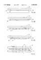
- FIG. 1illustrates a preferred embodiment of integrated circuit device constructed and operative in accordance with a preferred embodiment of the present invention and includes a relatively thin and compact, environmentally protected and mechanically strengthened integrated circuit package 10 having a multiplicity of electrical contacts 12 plated along the edge surfaces 14 thereof.
- contacts 12extend over edge surfaces onto the planar surfaces 16 of the package. This contact arrangement permits both flat surface mounting and edge mounting of package 10 onto a circuit board.
- the integrated circuit package 10may include an integrally formed ground plane (not shown) as well as ground plane contacts 18.
- the integrated circuit package 10may also include one or more thermal bonding pads 19 formed on one or both of the planar surfaces 16 thereof.
- the provision of such thermal bonding pads 19is optional.
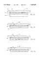
- a complete semiconductor substrate wafer 20 having a plurality of finished dies 22 formed thereon by conventional techniquesis bonded at its active surface 24 to an insulating cover plate 26 via a layer 28 of epoxy.
- the insulating cover plate 26typically comprises glass, alumina, beryllia, sapphire or any other suitable insulative substrate.
- Cover plate 26may be transparent to radiation in a spectral region useful for optical or infrared alignment.
- the complete semiconductor substrate wafer 20may be formed with an integral ground plane by conventional lithography techniques at any suitable location therein.
- a ground planemay be deposited and configured by conventional techniques over the active surface 24, such that the ground plane lies between active surface 24 and the epoxy layer 28.
- the semiconductor substrate waferis preferably ground down to a decreased thickness, typically 200 microns, as shown in FIG. 4B. This reduction in wafer thickness is enabled by the additional mechanical strength provided by the bonding thereof of the insulating cover plate 26.
- the waferis scribed along its back surface along predetermined dice lines which separate the individual dies.
- the scribed channels 30are of sufficient depth to reduce the wafer thickness thereunder to typically 100 microns.
- the scribed waferis shown in FIG. 3 and in FIG. 4C.
- the scribed waferis then etched in a conventional semiconductor substrate etching solution, which for silicon may be a combination of 24% potassium hydroxide (KOH), 63% water and 13% isopropanol, so as to etch the silicon down to the field oxide layer, as shown in FIG. 4D and more particularly in FIG. 5.
- a conventional semiconductor substrate etching solutionwhich for silicon may be a combination of 24% potassium hydroxide (KOH), 63% water and 13% isopropanol, so as to etch the silicon down to the field oxide layer, as shown in FIG. 4D and more particularly in FIG. 5.
- At least one insulating layer, including the field oxide layer,is shown at reference numeral 32 and metal pads are shown at reference numeral 34.
- An over-metal insulating layeris shown at reference numeral 36.
- the ground planeis shown at reference numeral 38.
- the result of the semiconductor substrate etchingis a plurality of separated dies 40, each of which includes semiconductor substrate 39 of thickness about 100 microns.
- a second insulating packaging layer 42is bonded over the dies 40 on the side thereof opposite to insulating packaging layer 26.
- a layer 44 of epoxylies between the dies 40 and the layer 42 and epoxy also fills the interstices between dies 40.
- the sandwich of the dies 40, and the first and second insulating packaging layers 26 and 42is then diced along lines 50, lying along the interstices between adjacent dies 40 to define a plurality of pre-packaged integrated circuits. It is a particular feature of the invention that lines 50 are selected such that the edges of the diced chips are distanced from the outer extent of the semiconductor substrate 39 by at least a distance d, as shown in FIGS. 4E and 5.
- dicing of the sandwich of FIG. 4E along lines 50exposes edges of a multiplicity of pads 34 on the wafer 20, which pad edges, when so exposed, define contact surfaces 51 of dies 40. Dicing of the sandwich of FIG. 4E also exposes edge portions of the ground plane 38 which define ground plane contact surfaces 52.
- FIG. 6illustrates an individual pre-packaged die following dicing.
- the entire integrated circuit deviceis peripherally sealed by epoxy 53 between insulating packaging layers 26 and 42 which define the integrated circuit package.
- all or part of the die or at least the edges thereofis coated with a conductive coating, such as aluminum, as by vacuum deposition.
- a conductive coatingsuch as aluminum, as by vacuum deposition.
- this conductive coatingis selectively etched, as indicated in FIG. 7 to define mutually electrically insulated conductive strips 62, each of which electrically communicates with a different contact surface 51 or 52.
- the thermal bonding pads 19may also be defined at this stage.
- FIG. 8illustrates an alternative embodiment of the present invention wherein all of the contact strips appear on at least one edge 70 thereof, which edge may then be surface mounted onto a printed circuit board, for providing vertical mounting of the integrated circuit device.
- the illustrated embodimentprovides conductive pathways 72 communicating between individual contact surfaces 51 on various edges of the device and contact strips 74 on edge 70. Such pathways may be formed on one or both of the planar surfaces of the integrated circuit package.
- FIG. 9illustrates another optional feature of the present invention.
- substrate isolation of part of an integrated circuit diemay be readily provided by adding extra scribe lines and etching therealong as illustrated in FIGS. 4C and 4D, but within a given die boundary, rather than along die boundaries. Following such scribing and etching the separation between adjacent portions 76 of the semiconductor substrate substrate is filled with epoxy 78.
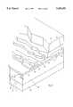
- FIG. 10is an illustration of a multi-die integrated circuit package 100 constructed and operative in accordance with a preferred embodiment of the invention.
- the embodiment of FIG. 10includes a plurality of dies 102, preferably arranged in a stacked arrangement.
- Each die 102may have an identical or different circuit thereon.
- the diesmay be stacked one upon another in electrically insulative relationship, with or without the interposition of additional insulative layers therebetween.
- the multi-die integrated circuit package 100is relatively thin and compact, environmentally protected and mechanically strengthened and has a multiplicity of electrical contacts 112 plated along the edge surfaces 114 thereof.
- contacts 112extend over edge surfaces onto the planar surfaces 116 of the package. This contact arrangement permits both flat surface mounting and edge mounting of package 100 onto a circuit board.
- the integrated circuit package 100may include one or more integrally formed ground planes (not shown) as well as ground plane contacts 118. Additionally, one or more specific dies, such as an ASIC, for providing complex interconnect functions may be interposed among the stacked integrated circuits.
- the integrated circuit package 100may also include one or more thermal bonding pads 119 formed on one or both of the planar surfaces 116 thereof.
- the provision of such thermal bonding pads 119is optional.
- FIGS. 11A, 11B, 11C, 11D, 11E, 11F, 11G, 11H, 11I, 11J, 11K, 11L and 11Mare sectional illustrations of various stages in the manufacture of multi-die integrated circuit devices in accordance with a preferred embodiment of the present invention.
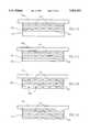
- a complete semiconductor substrate wafer 120 having a plurality of dies 122 formed thereon by conventional techniquesis bonded at its active surface 124 to an insulating cover plate 126 via a layer 128 of epoxy.
- the insulating cover plate 126typically comprises glass, alumina, beryllia, sapphire or any other suitable insulative substrate.
- the complete semiconductor substrate wafer 120may be formed with an integral ground plane by conventional techniques at any suitable location therein.
- a ground planemay be deposited and configured by conventional techniques over the active surface 124, such that the ground plane lies between active surface 124 and the epoxy layer 128.
- the semiconductor substrate waferis preferably ground down to a decreased thickness, typically 200 microns, as shown in FIG. 11B.
- the waferis scribed along its back surface along predetermined dice lines which separate the individual dies.
- the scribed channels 130are of sufficient depth to reduce the wafer thickness thereunder to typically 100 microns.
- the scribed waferis shown in FIG. 11C.
- the scribed waferis then etched in a conventional semiconductor substrate etching solution, such as that described hereinabove, so as to etch the semiconductor substrate down to the field oxide layer, as shown in FIG. 11D.
- each dieis configured generally as shown in FIG. 5, described above.
- an additional wafer 150is bonded over scribed and etched dies 122, as illustrated in FIG. 11E, the epoxy 152 which is used for the bonding, filling in the interstices between semiconductor substrate substrates of adjacent dies 122 and thus providing isolation thereof in addition to that provided by the oxide passivation layer on each die.
- wafer 150is reduced, as shown in FIG. 11F and wafer 150 is scribed and then etched, as shown in FIGS. 11G and 11H respectively and as described hereinabove in connection with FIGS. 4B-4D.
- an additional wafer 160is bonded over scribed and etched wafer 150, as illustrated in FIG. 11I, the epoxy 162 which is used for the bonding, filling in the interstices between semiconductor substrate substrates of adjacent dies 163 on wafer 150 and thus providing isolation thereof.
- wafer 160is reduced, as shown in FIG. 11J and wafer 160 is scribed and then etched, as shown in FIGS. 11K and 11L respectively and as described hereinabove in connection with FIGS. 4B-4D.
- a second insulating packaging layer 170is bonded thereto, as shown in FIG. 11M.
- a layer 172 of epoxylies between the dies 174 on the last wafer and the layer 170 and the epoxy also fills the interstices between dies 174.
- the sandwich of the plurality of wafers and the first and second insulating packaging layers 126 and 170is then diced along lines lying along the interstices between the adjacent dies on each wafer to define a plurality of pre-packaged integrated circuits.
- dicing of the sandwich of FIGS. 4E and 11Mexposes edges of a multiplicity of pads on the wafers, which pad edges, when so exposed, define contact surfaces. These contact surfaces are preferably subjected to an anti-corrosion treatment. Dicing of the sandwich of FIG. 11M also exposes edge portions of the ground plane which define ground plane contact surfaces, which are also preferably subject to anti-corrosion treatment. Other than the exposed contact surfaces, the entire integrated circuit device is peripherally sealed by epoxy between insulating packaging layers 126 and 170 which define the integrated circuit package.
- a conductive coatingsuch as aluminum, as by vacuum deposition.
- this conductive coatingis selectively etched, as indicated in FIG. 10 to define mutually electrically insulated conductive strips 112, each of which electrically communicates with a different contact surface.
- Conductive strips 112may provide interconnection between the various dies as well as interconnection with external circuits.
- Ground plane contacts 118 and thermal bonding pads 119may also be defined at this stage.
- the conductive layersare preferably nickel coated and may also be gold plated and/or solder coated by conventional techniques. Suitable anti-corrosion treatments may also be provided. It is noted that the stacked integrated circuit package described hereinabove need not necessarily be formed of integrated circuit dies from a single whole wafer or even from the same wafer. The integrated circuit dies which are combined in the stack may be formed individually or in groups by any suitable technique. The integrated circuit dies preferably pass a sorting stage prior to being incorporated in a stack, in order to increase stack yield.
- Improved heat dissipation in the stackmay be achieved by incorporating insulative high thermal conductivity substrates in the die stack.
- FIGS. 12A and 12Billustrate apparatus for producing integrated circuit devices in accordance with a preferred embodiment of the present invention.
- a conventional wafer fabrication facility 180provides complete wafers 20. Individual wafers 20 are bonded on their active surfaces by bonding apparatus 182, preferably having facilities for rotation of the wafer 20, the layer 26 and the epoxy 28 so as to obtain even distribution of the epoxy.
- the bonded wafer(FIG. 3) is thinned at its non-active surface as by grinding apparatus 184, such as Model 32BTGW using 12.5A abrasive, which is commercially available from Speedfam Machines Co. Ltd. of England.
- the waferis then scribed at its non-active surface by scribing apparatus 186 such as a Kulicke & Soffa 775 dicing saw employing an Ni plated diamond loaded blade, producing a result which is shown in FIG. 4C.
- scribing apparatus 186such as a Kulicke & Soffa 775 dicing saw employing an Ni plated diamond loaded blade, producing a result which is shown in FIG. 4C.
- the scribed wafer of FIG. 4Cis then etched in a temperature controlled bath 188 containing a semiconductor substrate etch solution 190.
- a temperature controlled bath 188containing a semiconductor substrate etch solution 190.
- Commercially available equipment for this purposeinclude a Chemkleen bath and an WHRV circulator both of which are manufactured by Wafab Inc. of the U.S.A..
- a suitable conventional silicon etching solutionis Isoform Silicon etch, which is commercially available from Micro-Image Technology Ltd. of England.
- the waferis conventionally rinsed after etching.
- the resulting etched waferis shown in FIG. 4D.
- the etched waferis bonded on the non-active side to another protective layer 42 by bonding apparatus 192, which may be essentially the same as apparatus 182, to produce a doubly bonded wafer sandwich as shown in FIG. 4E.
- Dicing apparatus 194which may be identical to apparatus 186, dices the bonded wafer sandwich of FIG. 4E into individual dies.
- the dicing bladeshould be a diamond resinoid blade of thickness 4-12 mils. The resulting dies appear as illustrated generally in FIG. 6.
- the diced diesare then subjected to anti-corrosion treatment in a bath 196, containing a chromating solution 198, such as described in any of the following U.S. Pat. Nos.: 2,507,956; 2,851,385 and 2,796,370, the disclosure of which is hereby incorporated by reference.
- Conductive layer deposition apparatus 200which operates by vacuum deposition techniques, such as a Model 903M sputtering machine manufactured by Material Research Corporation of the U.S.A., is employed to produce a conductive layer on one or more surfaces of the die of FIG. 6.
- Configuration of contact stripsis carried out preferably by using conventional electro-deposited photoresist, which is commercially available from DuPont under the brand name Primecoat or from Shipley, under the brand name Eagle.
- the photoresistis applied to the dies in a photoresist bath assembly 202 which is commercially available from DuPont or Shipley.
- the photoresistis preferably laser configured by a suitable laser scanner 204 to define suitable etching patterns.
- the photoresistis then developed in a development bath 206, and then etched in a metal etch solution 208 located in an etching bath 210, thus providing a conductor configuration such as that shown in FIG. 7.
- the exposed conductive strips shown in FIG. 7are then plated, preferably by electroless plating apparatus 212, which is commercially available from Okuno of Japan.
- conductive stripsmay be achieved by techniques other than photolithography. Any suitable technique, such as direct writing, may alternatively be employed.
Landscapes
- Engineering & Computer Science (AREA)
- Microelectronics & Electronic Packaging (AREA)
- Power Engineering (AREA)
- Computer Hardware Design (AREA)
- General Physics & Mathematics (AREA)
- Condensed Matter Physics & Semiconductors (AREA)
- Physics & Mathematics (AREA)
- Manufacturing & Machinery (AREA)
- Design And Manufacture Of Integrated Circuits (AREA)
- Semiconductor Integrated Circuits (AREA)
- Dicing (AREA)
- Encapsulation Of And Coatings For Semiconductor Or Solid State Devices (AREA)
- Bipolar Transistors (AREA)
- Internal Circuitry In Semiconductor Integrated Circuit Devices (AREA)
- Junction Field-Effect Transistors (AREA)
Abstract
Description
Claims (46)
Priority Applications (1)
| Application Number | Priority Date | Filing Date | Title |
|---|---|---|---|
| US08/274,251US5547906A (en) | 1992-09-14 | 1994-07-13 | Methods for producing integrated circuit devices |
Applications Claiming Priority (1)
| Application Number | Priority Date | Filing Date | Title |
|---|---|---|---|
| PCT/EP1992/002134WO1994007267A1 (en) | 1992-09-14 | 1992-09-14 | Methods and apparatus for producing integrated circuit devices |
Related Child Applications (1)
| Application Number | Title | Priority Date | Filing Date |
|---|---|---|---|
| US08/274,251DivisionUS5547906A (en) | 1992-09-14 | 1994-07-13 | Methods for producing integrated circuit devices |
Publications (1)
| Publication Number | Publication Date |
|---|---|
| US5455455Atrue US5455455A (en) | 1995-10-03 |
Family
ID=8165681
Family Applications (2)
| Application Number | Title | Priority Date | Filing Date |
|---|---|---|---|
| US07/962,222Expired - LifetimeUS5455455A (en) | 1992-09-14 | 1992-09-14 | Methods for producing packaged integrated circuit devices and packaged integrated circuit devices produced thereby |
| US08/274,251Expired - LifetimeUS5547906A (en) | 1992-09-14 | 1994-07-13 | Methods for producing integrated circuit devices |
Family Applications After (1)
| Application Number | Title | Priority Date | Filing Date |
|---|---|---|---|
| US08/274,251Expired - LifetimeUS5547906A (en) | 1992-09-14 | 1994-07-13 | Methods for producing integrated circuit devices |
Country Status (23)
| Country | Link |
|---|---|
| US (2) | US5455455A (en) |
| EP (1) | EP0660967B1 (en) |
| JP (1) | JP3621093B2 (en) |
| KR (1) | KR100310220B1 (en) |
| AT (1) | ATE200593T1 (en) |
| AU (1) | AU2554192A (en) |
| BG (1) | BG99554A (en) |
| CA (1) | CA2144323C (en) |
| DE (1) | DE69231785T2 (en) |
| DK (1) | DK0660967T3 (en) |
| EC (1) | ECSP930975A (en) |
| FI (1) | FI951142L (en) |
| GT (1) | GT199300053A (en) |
| HU (1) | HUT73312A (en) |
| IL (1) | IL106710A (en) |
| MA (1) | MA25277A1 (en) |
| MX (1) | MX9305603A (en) |
| MY (1) | MY129454A (en) |
| NO (1) | NO950960L (en) |
| PL (1) | PL169823B1 (en) |
| PT (1) | PT101354A (en) |
| WO (1) | WO1994007267A1 (en) |
| ZA (1) | ZA936039B (en) |
Cited By (106)
| Publication number | Priority date | Publication date | Assignee | Title |
|---|---|---|---|---|
| US5547906A (en)* | 1992-09-14 | 1996-08-20 | Badehi; Pierre | Methods for producing integrated circuit devices |
| US5716759A (en)* | 1993-09-02 | 1998-02-10 | Shellcase Ltd. | Method and apparatus for producing integrated circuit devices |
| US5765280A (en)* | 1996-02-02 | 1998-06-16 | National Semiconductor Corporation | Method for making a carrier based IC packaging arrangement |
| US5818107A (en)* | 1997-01-17 | 1998-10-06 | International Business Machines Corporation | Chip stacking by edge metallization |
| US5851845A (en)* | 1995-12-18 | 1998-12-22 | Micron Technology, Inc. | Process for packaging a semiconductor die using dicing and testing |
| US5863813A (en)* | 1997-08-20 | 1999-01-26 | Micron Communications, Inc. | Method of processing semiconductive material wafers and method of forming flip chips and semiconductor chips |
| US5903437A (en)* | 1997-01-17 | 1999-05-11 | International Business Machines Corporation | High density edge mounting of chips |
| US5930652A (en)* | 1996-05-28 | 1999-07-27 | Motorola, Inc. | Semiconductor encapsulation method |
| US5953588A (en)* | 1996-12-21 | 1999-09-14 | Irvine Sensors Corporation | Stackable layers containing encapsulated IC chips |
| US6008070A (en)* | 1998-05-21 | 1999-12-28 | Micron Technology, Inc. | Wafer level fabrication and assembly of chip scale packages |
| US6040235A (en)* | 1994-01-17 | 2000-03-21 | Shellcase Ltd. | Methods and apparatus for producing integrated circuit devices |
| US6117707A (en)* | 1994-07-13 | 2000-09-12 | Shellcase Ltd. | Methods of producing integrated circuit devices |
| US6169319B1 (en) | 1999-08-12 | 2001-01-02 | Tower Semiconductor Ltd. | Backside illuminated image sensor |
| US6184063B1 (en)* | 1996-11-26 | 2001-02-06 | Texas Instruments Incorporated | Method and apparatus for breaking and separating a wafer into die using a multi-radii dome |
| US6227941B1 (en)* | 1998-11-17 | 2001-05-08 | Advanced Micro Devices, Inc. | Support structure with multi-layer support material for use during package removal from a multi-layer integrated circuit device |
| US20010003049A1 (en)* | 1996-07-12 | 2001-06-07 | Norio Fukasawa | Method and mold for manufacturing semiconductor device, semiconductor device, and method for mounting the device |
| US20010018236A1 (en)* | 1999-12-10 | 2001-08-30 | Shellcase Ltd. | Methods for producing packaged integrated circuit devices & packaged integrated circuit devices produced thereby |
| US6452265B1 (en) | 2000-01-28 | 2002-09-17 | International Business Machines Corporation | Multi-chip module utilizing a nonconductive material surrounding the chips that has a similar coefficient of thermal expansion |
| US6452260B1 (en) | 1997-09-02 | 2002-09-17 | Silicon Light Machines | Electrical interface to integrated circuit device having high density I/O count |
| US6483736B2 (en) | 1998-11-16 | 2002-11-19 | Matrix Semiconductor, Inc. | Vertically stacked field programmable nonvolatile memory and method of fabrication |
| US6525953B1 (en) | 2001-08-13 | 2003-02-25 | Matrix Semiconductor, Inc. | Vertically-stacked, field-programmable, nonvolatile memory and method of fabrication |
| DE10153609A1 (en)* | 2001-11-02 | 2003-05-15 | Infineon Technologies Ag | Production of an electronic component used in chip technology comprises forming a first planar chip arrangement, forming a further planar chip arrangement, optionally applying interconnecting elements and forming electronic components |
| US20030151124A1 (en)* | 1998-02-06 | 2003-08-14 | Shellcase, Ltd. | Integrated circuit device |
| US20030216010A1 (en)* | 2002-05-20 | 2003-11-20 | Eugene Atlas | Forming a multi segment integrated circuit with isolated substrates |
| US20040021214A1 (en)* | 2002-04-16 | 2004-02-05 | Avner Badehi | Electro-optic integrated circuits with connectors and methods for the production thereof |
| US6707591B2 (en) | 2001-04-10 | 2004-03-16 | Silicon Light Machines | Angled illumination for a single order light modulator based projection system |
| US20040053434A1 (en)* | 2001-09-13 | 2004-03-18 | Silicon Light Machines | Microelectronic mechanical system and methods |
| US6714418B2 (en) | 2001-11-02 | 2004-03-30 | Infineon Technologies Ag | Method for producing an electronic component having a plurality of chips that are stacked one above the other and contact-connected to one another |
| US6712480B1 (en) | 2002-09-27 | 2004-03-30 | Silicon Light Machines | Controlled curvature of stressed micro-structures |
| US6728023B1 (en) | 2002-05-28 | 2004-04-27 | Silicon Light Machines | Optical device arrays with optimized image resolution |
| US6747781B2 (en) | 2001-06-25 | 2004-06-08 | Silicon Light Machines, Inc. | Method, apparatus, and diffuser for reducing laser speckle |
| US6764875B2 (en) | 1998-07-29 | 2004-07-20 | Silicon Light Machines | Method of and apparatus for sealing an hermetic lid to a semiconductor die |
| US6767751B2 (en) | 2002-05-28 | 2004-07-27 | Silicon Light Machines, Inc. | Integrated driver process flow |
| US6782205B2 (en) | 2001-06-25 | 2004-08-24 | Silicon Light Machines | Method and apparatus for dynamic equalization in wavelength division multiplexing |
| US20040183185A1 (en)* | 1998-02-06 | 2004-09-23 | Avner Badihi | Packaged integrated circuits and methods of producing thereof |
| US6801354B1 (en) | 2002-08-20 | 2004-10-05 | Silicon Light Machines, Inc. | 2-D diffraction grating for substantially eliminating polarization dependent losses |
| US6800238B1 (en) | 2002-01-15 | 2004-10-05 | Silicon Light Machines, Inc. | Method for domain patterning in low coercive field ferroelectrics |
| US6806997B1 (en) | 2003-02-28 | 2004-10-19 | Silicon Light Machines, Inc. | Patterned diffractive light modulator ribbon for PDL reduction |
| US6813059B2 (en) | 2002-06-28 | 2004-11-02 | Silicon Light Machines, Inc. | Reduced formation of asperities in contact micro-structures |
| US6822797B1 (en) | 2002-05-31 | 2004-11-23 | Silicon Light Machines, Inc. | Light modulator structure for producing high-contrast operation using zero-order light |
| US6829092B2 (en) | 2001-08-15 | 2004-12-07 | Silicon Light Machines, Inc. | Blazed grating light valve |
| US6829077B1 (en) | 2003-02-28 | 2004-12-07 | Silicon Light Machines, Inc. | Diffractive light modulator with dynamically rotatable diffraction plane |
| US6829258B1 (en) | 2002-06-26 | 2004-12-07 | Silicon Light Machines, Inc. | Rapidly tunable external cavity laser |
| US6841813B2 (en) | 2001-08-13 | 2005-01-11 | Matrix Semiconductor, Inc. | TFT mask ROM and method for making same |
| US6865346B1 (en) | 2001-06-05 | 2005-03-08 | Silicon Light Machines Corporation | Fiber optic transceiver |
| US6872984B1 (en) | 1998-07-29 | 2005-03-29 | Silicon Light Machines Corporation | Method of sealing a hermetic lid to a semiconductor die at an angle |
| US6881611B1 (en)* | 1996-07-12 | 2005-04-19 | Fujitsu Limited | Method and mold for manufacturing semiconductor device, semiconductor device and method for mounting the device |
| US6897514B2 (en) | 2001-03-28 | 2005-05-24 | Matrix Semiconductor, Inc. | Two mask floating gate EEPROM and method of making |
| US6908201B2 (en) | 2002-06-28 | 2005-06-21 | Silicon Light Machines Corporation | Micro-support structures |
| US20050158899A1 (en)* | 2002-03-18 | 2005-07-21 | Sarcos Investments Lc | Miniaturized imaging device with integrated circuit connector system |
| US6922273B1 (en) | 2003-02-28 | 2005-07-26 | Silicon Light Machines Corporation | PDL mitigation structure for diffractive MEMS and gratings |
| US6922272B1 (en) | 2003-02-14 | 2005-07-26 | Silicon Light Machines Corporation | Method and apparatus for leveling thermal stress variations in multi-layer MEMS devices |
| US6927891B1 (en) | 2002-12-23 | 2005-08-09 | Silicon Light Machines Corporation | Tilt-able grating plane for improved crosstalk in 1×N blaze switches |
| US6928207B1 (en) | 2002-12-12 | 2005-08-09 | Silicon Light Machines Corporation | Apparatus for selectively blocking WDM channels |
| US6934070B1 (en) | 2002-12-18 | 2005-08-23 | Silicon Light Machines Corporation | Chirped optical MEM device |
| WO2005083779A1 (en)* | 2004-02-25 | 2005-09-09 | Infineon Technologies Ag | Rear-coated thin semiconductor chip, and method for the production thereof |
| US6947613B1 (en) | 2003-02-11 | 2005-09-20 | Silicon Light Machines Corporation | Wavelength selective switch and equalizer |
| US6956995B1 (en) | 2001-11-09 | 2005-10-18 | Silicon Light Machines Corporation | Optical communication arrangement |
| US6956878B1 (en) | 2000-02-07 | 2005-10-18 | Silicon Light Machines Corporation | Method and apparatus for reducing laser speckle using polarization averaging |
| US6987600B1 (en) | 2002-12-17 | 2006-01-17 | Silicon Light Machines Corporation | Arbitrary phase profile for better equalization in dynamic gain equalizer |
| US20060022289A1 (en)* | 2002-04-16 | 2006-02-02 | Xloom Photonics, Ltd. | Electro-optical circuitry having integrated connector and methods for the production thereof |
| US7027202B1 (en) | 2003-02-28 | 2006-04-11 | Silicon Light Machines Corp | Silicon substrate as a light modulator sacrificial layer |
| US7033664B2 (en) | 2002-10-22 | 2006-04-25 | Tessera Technologies Hungary Kft | Methods for producing packaged integrated circuit devices and packaged integrated circuit devices produced thereby |
| US7042611B1 (en) | 2003-03-03 | 2006-05-09 | Silicon Light Machines Corporation | Pre-deflected bias ribbons |
| US7054515B1 (en) | 2002-05-30 | 2006-05-30 | Silicon Light Machines Corporation | Diffractive light modulator-based dynamic equalizer with integrated spectral monitor |
| US7057819B1 (en) | 2002-12-17 | 2006-06-06 | Silicon Light Machines Corporation | High contrast tilting ribbon blazed grating |
| US7057795B2 (en) | 2002-08-20 | 2006-06-06 | Silicon Light Machines Corporation | Micro-structures with individually addressable ribbon pairs |
| US7068372B1 (en) | 2003-01-28 | 2006-06-27 | Silicon Light Machines Corporation | MEMS interferometer-based reconfigurable optical add-and-drop multiplexor |
| US20060138626A1 (en)* | 2004-12-29 | 2006-06-29 | Tessera, Inc. | Microelectronic packages using a ceramic substrate having a window and a conductive surface region |
| US7177081B2 (en) | 2001-03-08 | 2007-02-13 | Silicon Light Machines Corporation | High contrast grating light valve type device |
| US20070034777A1 (en)* | 2005-08-12 | 2007-02-15 | Tessera, Inc. | Image sensor employing a plurality of photodetector arrays and/or rear-illuminated architecture |
| US7286764B1 (en) | 2003-02-03 | 2007-10-23 | Silicon Light Machines Corporation | Reconfigurable modulator-based optical add-and-drop multiplexer |
| US20080099907A1 (en)* | 2006-10-31 | 2008-05-01 | Tessera Technologies Hungary Kft. | Wafer-level fabrication of lidded chips with electrodeposited dielectric coating |
| US20080099900A1 (en)* | 2006-10-31 | 2008-05-01 | Tessera Technologies Hungary Kft. | Wafer-level fabrication of lidded chips with electrodeposited dielectric coating |
| US7391973B1 (en) | 2003-02-28 | 2008-06-24 | Silicon Light Machines Corporation | Two-stage gain equalizer |
| US20080258306A1 (en)* | 2007-04-19 | 2008-10-23 | Siliconware Precision Industries Co., Ltd. | Semiconductor Device and Method for Fabricating the Same |
| US20080315424A1 (en)* | 2001-03-30 | 2008-12-25 | Megica Corporation | Structure and manufactruing method of chip scale package |
| US20090034085A1 (en)* | 2003-10-15 | 2009-02-05 | Xloom Communications, Ltd. | Electro-optical circuitry having integrated connector and methods for the production thereof |
| US20090093137A1 (en)* | 2007-10-08 | 2009-04-09 | Xloom Communications, (Israel) Ltd. | Optical communications module |
| US20090213542A1 (en)* | 2008-02-22 | 2009-08-27 | Seagate Technology Llc | Flex circuit assembly with thermal energy dissipation |
| US20090261476A1 (en)* | 2007-04-18 | 2009-10-22 | Siliconware Precision Industries Co., Ltd. | Semiconductor device and manufacturing method thereof |
| US7787939B2 (en) | 2002-03-18 | 2010-08-31 | Sterling Lc | Miniaturized imaging device including utility aperture and SSID |
| US20100233854A1 (en)* | 2009-03-12 | 2010-09-16 | Utac Thai Limited | Metallic solderability preservation coating on metal part of semiconductor package to prevent oxide |
| US7825455B2 (en) | 2000-08-14 | 2010-11-02 | Sandisk 3D Llc | Three terminal nonvolatile memory device with vertical gated diode |
| US7835074B2 (en) | 2007-06-05 | 2010-11-16 | Sterling Lc | Mini-scope for multi-directional imaging |
| US7960272B2 (en) | 2002-10-24 | 2011-06-14 | Megica Corporation | Method for fabricating thermal compliant semiconductor chip wiring structure for chip scale packaging |
| US7969659B2 (en) | 2008-01-11 | 2011-06-28 | Sterling Lc | Grin lens microscope system |
| US20130069086A1 (en)* | 2010-02-24 | 2013-03-21 | Osram Opto Semiconductors Gmbh | Method for producing a plurality of optoelectronic semiconductor chips |
| US8486735B2 (en) | 2008-07-30 | 2013-07-16 | Raytheon Company | Method and device for incremental wavelength variation to analyze tissue |
| US8614768B2 (en) | 2002-03-18 | 2013-12-24 | Raytheon Company | Miniaturized imaging device including GRIN lens optically coupled to SSID |
| US8669777B2 (en) | 2010-10-27 | 2014-03-11 | Seagate Technology Llc | Assessing connection joint coverage between a device and a printed circuit board |
| US8690762B2 (en) | 2008-06-18 | 2014-04-08 | Raytheon Company | Transparent endoscope head defining a focal length |
| US8717428B2 (en) | 2009-10-01 | 2014-05-06 | Raytheon Company | Light diffusion apparatus |
| US8759148B2 (en) | 2009-01-27 | 2014-06-24 | Panasonic Corporation | Method of mounting semiconductor chips, semiconductor device obtained using the method, method of connecting semiconductor chips, three-dimensional structure in which wiring is provided on its surface, and method of producing the same |
| US8828028B2 (en) | 2009-11-03 | 2014-09-09 | Raytheon Company | Suture device and method for closing a planar opening |
| US9060704B2 (en) | 2008-11-04 | 2015-06-23 | Sarcos Lc | Method and device for wavelength shifted imaging |
| US9070393B2 (en) | 2009-01-27 | 2015-06-30 | Panasonic Corporation | Three-dimensional structure in which wiring is provided on its surface |
| US9082438B2 (en) | 2008-12-02 | 2015-07-14 | Panasonic Corporation | Three-dimensional structure for wiring formation |
| US9144664B2 (en) | 2009-10-01 | 2015-09-29 | Sarcos Lc | Method and apparatus for manipulating movement of a micro-catheter |
| US9478503B2 (en) | 2012-03-30 | 2016-10-25 | Tohoku University | Integrated device |
| US20170053855A1 (en)* | 2015-08-21 | 2017-02-23 | Nxp B.V. | Electronic device and method of making same |
| US9661996B2 (en) | 2009-10-01 | 2017-05-30 | Sarcos Lc | Needle delivered imaging device |
| US10242934B1 (en) | 2014-05-07 | 2019-03-26 | Utac Headquarters Pte Ltd. | Semiconductor package with full plating on contact side surfaces and methods thereof |
| US10242953B1 (en) | 2015-05-27 | 2019-03-26 | Utac Headquarters PTE. Ltd | Semiconductor package with plated metal shielding and a method thereof |
| US10468400B2 (en) | 2017-02-03 | 2019-11-05 | Samsung Electronics Co., Ltd. | Method of manufacturing substrate structure |
| US20220310821A1 (en)* | 2021-03-29 | 2022-09-29 | Littelfuse Semiconductor (Wuxi) Co., Ltd. | Semiconductor mesa device formation method |
Families Citing this family (59)
| Publication number | Priority date | Publication date | Assignee | Title |
|---|---|---|---|---|
| US5904546A (en)* | 1996-02-12 | 1999-05-18 | Micron Technology, Inc. | Method and apparatus for dicing semiconductor wafers |
| US5952725A (en) | 1996-02-20 | 1999-09-14 | Micron Technology, Inc. | Stacked semiconductor devices |
| US5682065A (en)* | 1996-03-12 | 1997-10-28 | Micron Technology, Inc. | Hermetic chip and method of manufacture |
| FR2748350B1 (en)* | 1996-05-06 | 2000-07-13 | Solaic Sa | ELECTRONIC COMPONENT IN THE FORM OF AN INTEGRATED CIRCUIT FOR HOT INSERTION IN A SUBSTRATE AND METHODS OF MAKING SAME |
| US6784023B2 (en)* | 1996-05-20 | 2004-08-31 | Micron Technology, Inc. | Method of fabrication of stacked semiconductor devices |
| WO1997047040A1 (en)* | 1996-05-30 | 1997-12-11 | Shellcase Ltd. | I.c. device with concealed conductor lines |
| US5956605A (en)* | 1996-09-20 | 1999-09-21 | Micron Technology, Inc. | Use of nitrides for flip-chip encapsulation |
| US6077757A (en)* | 1997-05-15 | 2000-06-20 | Nec Corporation | Method of forming chip semiconductor devices |
| DE19739684B4 (en)* | 1997-09-10 | 2006-04-13 | Robert Bosch Gmbh | Process for the production of chip stacks |
| JP3526731B2 (en)* | 1997-10-08 | 2004-05-17 | 沖電気工業株式会社 | Semiconductor device and manufacturing method thereof |
| KR100273704B1 (en)* | 1997-12-20 | 2000-12-15 | 윤종용 | Method for fabricating semiconductor substrate |
| JP3514101B2 (en)* | 1998-01-28 | 2004-03-31 | セイコーエプソン株式会社 | Semiconductor device, method of manufacturing the same, and electronic equipment |
| JP2000012745A (en)* | 1998-06-24 | 2000-01-14 | Nec Corp | Semiconductor package and its manufacture |
| KR100269540B1 (en)* | 1998-08-28 | 2000-10-16 | 윤종용 | Method for manufacturing chip scale packages at wafer level |
| US6903451B1 (en) | 1998-08-28 | 2005-06-07 | Samsung Electronics Co., Ltd. | Chip scale packages manufactured at wafer level |
| US6339251B2 (en) | 1998-11-10 | 2002-01-15 | Samsung Electronics Co., Ltd | Wafer grooves for reducing semiconductor wafer warping |
| FR2788375B1 (en) | 1999-01-11 | 2003-07-18 | Gemplus Card Int | INTEGRATED CIRCUIT CHIP PROTECTION METHOD |
| JP3556503B2 (en)* | 1999-01-20 | 2004-08-18 | 沖電気工業株式会社 | Method for manufacturing resin-encapsulated semiconductor device |
| US6182342B1 (en) | 1999-04-02 | 2001-02-06 | Andersen Laboratories, Inc. | Method of encapsulating a saw device |
| US6544880B1 (en)* | 1999-06-14 | 2003-04-08 | Micron Technology, Inc. | Method of improving copper interconnects of semiconductor devices for bonding |
| JP2001094005A (en)* | 1999-09-22 | 2001-04-06 | Oki Electric Ind Co Ltd | Semiconductor device and method for producing it |
| DE10006738C2 (en)* | 2000-02-15 | 2002-01-17 | Osram Opto Semiconductors Gmbh | Light-emitting component with improved light decoupling and method for its production |
| WO2001061765A1 (en)* | 2000-02-15 | 2001-08-23 | Osram Opto Semiconductors Gmbh | Semiconductor component which emits radiation, and method for producing the same |
| SG106050A1 (en)* | 2000-03-13 | 2004-09-30 | Megic Corp | Method of manufacture and identification of semiconductor chip marked for identification with internal marking indicia and protection thereof by non-black layer and device produced thereby |
| JP4403631B2 (en)* | 2000-04-24 | 2010-01-27 | ソニー株式会社 | Manufacturing method of chip-shaped electronic component and manufacturing method of pseudo wafer used for manufacturing the same |
| JP2001313350A (en)* | 2000-04-28 | 2001-11-09 | Sony Corp | Chip-shaped electronic component and its manufacturing method, and pseudo-wafer used for manufacture of chip- shaped electronic component and its manufacturing method |
| JP3631956B2 (en) | 2000-05-12 | 2005-03-23 | 富士通株式会社 | Semiconductor chip mounting method |
| DE20111659U1 (en)* | 2000-05-23 | 2001-12-13 | OSRAM Opto Semiconductors GmbH & Co. oHG, 93049 Regensburg | Component for optoelectronics |
| US6875640B1 (en)* | 2000-06-08 | 2005-04-05 | Micron Technology, Inc. | Stereolithographic methods for forming a protective layer on a semiconductor device substrate and substrates including protective layers so formed |
| JP2002043251A (en)* | 2000-07-25 | 2002-02-08 | Fujitsu Ltd | Semiconductor device manufacturing method and semiconductor device |
| US6524881B1 (en) | 2000-08-25 | 2003-02-25 | Micron Technology, Inc. | Method and apparatus for marking a bare semiconductor die |
| US20020117753A1 (en)* | 2001-02-23 | 2002-08-29 | Lee Michael G. | Three dimensional packaging |
| US6797537B2 (en)* | 2001-10-30 | 2004-09-28 | Irvine Sensors Corporation | Method of making stackable layers containing encapsulated integrated circuit chips with one or more overlaying interconnect layers |
| US7169685B2 (en) | 2002-02-25 | 2007-01-30 | Micron Technology, Inc. | Wafer back side coating to balance stress from passivation layer on front of wafer and be used as die attach adhesive |
| US20060146172A1 (en)* | 2002-03-18 | 2006-07-06 | Jacobsen Stephen C | Miniaturized utility device having integrated optical capabilities |
| US7152291B2 (en) | 2002-04-15 | 2006-12-26 | Avx Corporation | Method for forming plated terminations |
| DE10342980B3 (en)* | 2003-09-17 | 2005-01-05 | Disco Hi-Tec Europe Gmbh | Semiconductor chip stack formation method for manufacture of 3D-packages with function testing of chips for removal or unacceptable chips and replacement by acceptable chips |
| US20050064683A1 (en)* | 2003-09-19 | 2005-03-24 | Farnworth Warren M. | Method and apparatus for supporting wafers for die singulation and subsequent handling |
| US20050064679A1 (en)* | 2003-09-19 | 2005-03-24 | Farnworth Warren M. | Consolidatable composite materials, articles of manufacture formed therefrom, and fabrication methods |
| US7713841B2 (en)* | 2003-09-19 | 2010-05-11 | Micron Technology, Inc. | Methods for thinning semiconductor substrates that employ support structures formed on the substrates |
| TWI233170B (en)* | 2004-02-05 | 2005-05-21 | United Microelectronics Corp | Ultra-thin wafer level stack packaging method and structure using thereof |
| US7244665B2 (en)* | 2004-04-29 | 2007-07-17 | Micron Technology, Inc. | Wafer edge ring structures and methods of formation |
| US7547978B2 (en)* | 2004-06-14 | 2009-06-16 | Micron Technology, Inc. | Underfill and encapsulation of semiconductor assemblies with materials having differing properties |
| US7235431B2 (en) | 2004-09-02 | 2007-06-26 | Micron Technology, Inc. | Methods for packaging a plurality of semiconductor dice using a flowable dielectric material |
| TWI303870B (en)* | 2005-12-30 | 2008-12-01 | Advanced Semiconductor Eng | Structure and mtehod for packaging a chip |
| FR2905198B1 (en)* | 2006-08-22 | 2008-10-17 | 3D Plus Sa Sa | COLLECTIVE MANUFACTURING METHOD OF 3D ELECTRONIC MODULES |
| US7923298B2 (en)* | 2007-09-07 | 2011-04-12 | Micron Technology, Inc. | Imager die package and methods of packaging an imager die on a temporary carrier |
| EP2207200A1 (en)* | 2008-12-24 | 2010-07-14 | Nxp B.V. | Stack of molded integrated circuit dies with side surface contact tracks |
| EP2202789A1 (en)* | 2008-12-24 | 2010-06-30 | Nxp B.V. | Stack of molded integrated circuit dies with side surface contact tracks |
| US8232140B2 (en)* | 2009-03-27 | 2012-07-31 | Taiwan Semiconductor Manufacturing Company, Ltd. | Method for ultra thin wafer handling and processing |
| WO2011045836A1 (en) | 2009-10-14 | 2011-04-21 | 国立大学法人東北大学 | Sensor device and method for fabricating sensor device |
| WO2011110900A1 (en)* | 2010-03-12 | 2011-09-15 | Nxp B.V. | Stack of molded integrated circuit dies with side surface contact tracks |
| US9299640B2 (en) | 2013-07-16 | 2016-03-29 | Taiwan Semiconductor Manufacturing Co., Ltd. | Front-to-back bonding with through-substrate via (TSV) |
| US9929050B2 (en) | 2013-07-16 | 2018-03-27 | Taiwan Semiconductor Manufacturing Company, Ltd. | Mechanisms for forming three-dimensional integrated circuit (3DIC) stacking structure |
| US8860229B1 (en)* | 2013-07-16 | 2014-10-14 | Taiwan Semiconductor Manufacturing Co., Ltd. | Hybrid bonding with through substrate via (TSV) |
| US9087821B2 (en) | 2013-07-16 | 2015-07-21 | Taiwan Semiconductor Manufacturing Co., Ltd. | Hybrid bonding with through substrate via (TSV) |
| TWI657510B (en)* | 2014-10-02 | 2019-04-21 | 日商住友電木股份有限公司 | Method of manufacturing semiconductor device, and semiconductor device |
| KR101712396B1 (en) | 2014-12-30 | 2017-03-13 | 주식회사 유림기계 | The blade of a knife fixing mechanism of wood chipper |
| JP7613803B2 (en) | 2020-05-19 | 2025-01-15 | インテル エヌディーティーエム ユーエス エルエルシー | Organic spacers for integrated circuits |
Citations (19)
| Publication number | Priority date | Publication date | Assignee | Title |
|---|---|---|---|---|
| DE1591105A1 (en)* | 1967-12-06 | 1970-09-24 | Itt Ind Gmbh Deutsche | Method for manufacturing solid state circuits |
| US3644801A (en)* | 1971-01-21 | 1972-02-22 | Gary S Sheldon | Semiconductor passivating process and product |
| US4294092A (en)* | 1979-02-13 | 1981-10-13 | Gkn-Stenman Ab | Cylinder lock having spring-actuated pins |
| US4383886A (en)* | 1980-11-14 | 1983-05-17 | Tokyo Shibaura Denki Kabushiki Kaisha | Method of manufacturing a semiconductor element |
| WO1985002283A1 (en)* | 1983-11-07 | 1985-05-23 | Irvine Sensors Corporation | Detector array module-structure and fabrication |
| EP0211609A2 (en)* | 1985-08-01 | 1987-02-25 | Unilever Plc | Chemically sensitive semiconductor devices and their production |
| JPH0217644A (en)* | 1988-07-06 | 1990-01-22 | Hitachi Ltd | Integrated circuit |
| US4933898A (en)* | 1989-01-12 | 1990-06-12 | General Instrument Corporation | Secure integrated circuit chip with conductive shield |
| JPH02191358A (en)* | 1989-01-19 | 1990-07-27 | Toshiba Corp | Processing method of semiconductor elements |
| US4962249A (en)* | 1988-06-23 | 1990-10-09 | Mobil Oil Corporation | High VI lubricants from lower alkene oligomers |
| US4971930A (en)* | 1985-12-20 | 1990-11-20 | Sgs Microelectronics S.P.A. | EPROM semiconductor device erasable with ultraviolet rays and manufacturing process thereof |
| US4984358A (en)* | 1989-03-10 | 1991-01-15 | Microelectronics And Computer Technology Corporation | Method of assembling stacks of integrated circuit dies |
| US5104820A (en)* | 1989-07-07 | 1992-04-14 | Irvine Sensors Corporation | Method of fabricating electronic circuitry unit containing stacked IC layers having lead rerouting |
| EP0490739A1 (en)* | 1990-12-11 | 1992-06-17 | Thomson-Csf | Interconnection method and device for three-dimensional integrated circuits |
| US5126286A (en)* | 1990-10-05 | 1992-06-30 | Micron Technology, Inc. | Method of manufacturing edge connected semiconductor die |
| US5147815A (en)* | 1990-05-14 | 1992-09-15 | Motorola, Inc. | Method for fabricating a multichip semiconductor device having two interdigitated leadframes |
| US5185295A (en)* | 1990-05-16 | 1993-02-09 | Kabushiki Kaisha Toshiba | Method for dicing semiconductor substrates using a laser scribing and dual etch process |
| US5266833A (en)* | 1992-03-30 | 1993-11-30 | Capps David F | Integrated circuit bus structure |
| US5292686A (en)* | 1991-08-21 | 1994-03-08 | Triquint Semiconductor, Inc. | Method of forming substrate vias in a GaAs wafer |
Family Cites Families (10)
| Publication number | Priority date | Publication date | Assignee | Title |
|---|---|---|---|---|
| US2507956A (en)* | 1947-11-01 | 1950-05-16 | Lithographic Technical Foundat | Process of coating aluminum |
| NL201472A (en)* | 1952-04-03 | |||
| US2796370A (en)* | 1955-03-04 | 1957-06-18 | Charles W Ostrander | Composition and method for producing corrosion resistant protective coating on aluminum and aluminum alloys |
| US4900695A (en)* | 1986-12-17 | 1990-02-13 | Hitachi, Ltd. | Semiconductor integrated circuit device and process for producing the same |
| US4862249A (en)* | 1987-04-17 | 1989-08-29 | Xoc Devices, Inc. | Packaging system for stacking integrated circuits |
| US4794092A (en)* | 1987-11-18 | 1988-12-27 | Grumman Aerospace Corporation | Single wafer moated process |
| US4784721A (en)* | 1988-02-22 | 1988-11-15 | Honeywell Inc. | Integrated thin-film diaphragm; backside etch |
| FR2645681B1 (en)* | 1989-04-07 | 1994-04-08 | Thomson Csf | DEVICE FOR VERTICALLY INTERCONNECTING PADS OF INTEGRATED CIRCUITS AND ITS MANUFACTURING METHOD |
| ATE200593T1 (en)* | 1992-09-14 | 2001-04-15 | Shellcase Ltd | METHOD FOR PRODUCING INTEGRATED CIRCUIT ARRANGEMENTS |
| US5376235A (en)* | 1993-07-15 | 1994-12-27 | Micron Semiconductor, Inc. | Method to eliminate corrosion in conductive elements |
- 1992
- 1992-09-14ATAT92919323Tpatent/ATE200593T1/enactive
- 1992-09-14JPJP50772194Apatent/JP3621093B2/ennot_activeExpired - Lifetime
- 1992-09-14DEDE69231785Tpatent/DE69231785T2/ennot_activeExpired - Fee Related
- 1992-09-14MXMX9305603Apatent/MX9305603A/ennot_activeIP Right Cessation
- 1992-09-14WOPCT/EP1992/002134patent/WO1994007267A1/enactiveIP Right Grant
- 1992-09-14AUAU25541/92Apatent/AU2554192A/ennot_activeAbandoned
- 1992-09-14KRKR1019950700986Apatent/KR100310220B1/ennot_activeExpired - Lifetime
- 1992-09-14FIFI951142Apatent/FI951142L/ennot_activeApplication Discontinuation
- 1992-09-14CACA002144323Apatent/CA2144323C/ennot_activeExpired - Fee Related
- 1992-09-14PLPL92308140Apatent/PL169823B1/enunknown
- 1992-09-14EPEP92919323Apatent/EP0660967B1/ennot_activeExpired - Lifetime
- 1992-09-14USUS07/962,222patent/US5455455A/ennot_activeExpired - Lifetime
- 1992-09-14HUHU9500783Apatent/HUT73312A/enunknown
- 1992-09-14DKDK92919323Tpatent/DK0660967T3/enactive
- 1993
- 1993-08-16ILIL10671093Apatent/IL106710A/ennot_activeIP Right Cessation
- 1993-08-18ZAZA936039Apatent/ZA936039B/enunknown
- 1993-08-20ECEC1993000975Apatent/ECSP930975A/enunknown
- 1993-09-02PTPT101354Apatent/PT101354A/ennot_activeApplication Discontinuation
- 1993-09-09GTGT199300053Apatent/GT199300053A/enunknown
- 1993-09-13MAMA23286Apatent/MA25277A1/enunknown
- 1993-09-14MYMYPI93001866Apatent/MY129454A/enunknown
- 1994
- 1994-07-13USUS08/274,251patent/US5547906A/ennot_activeExpired - Lifetime
- 1995
- 1995-03-13NONO950960Apatent/NO950960L/enunknown
- 1995-04-10BGBG99554Apatent/BG99554A/enunknown
Patent Citations (19)
| Publication number | Priority date | Publication date | Assignee | Title |
|---|---|---|---|---|
| DE1591105A1 (en)* | 1967-12-06 | 1970-09-24 | Itt Ind Gmbh Deutsche | Method for manufacturing solid state circuits |
| US3644801A (en)* | 1971-01-21 | 1972-02-22 | Gary S Sheldon | Semiconductor passivating process and product |
| US4294092A (en)* | 1979-02-13 | 1981-10-13 | Gkn-Stenman Ab | Cylinder lock having spring-actuated pins |
| US4383886A (en)* | 1980-11-14 | 1983-05-17 | Tokyo Shibaura Denki Kabushiki Kaisha | Method of manufacturing a semiconductor element |
| WO1985002283A1 (en)* | 1983-11-07 | 1985-05-23 | Irvine Sensors Corporation | Detector array module-structure and fabrication |
| EP0211609A2 (en)* | 1985-08-01 | 1987-02-25 | Unilever Plc | Chemically sensitive semiconductor devices and their production |
| US4971930A (en)* | 1985-12-20 | 1990-11-20 | Sgs Microelectronics S.P.A. | EPROM semiconductor device erasable with ultraviolet rays and manufacturing process thereof |
| US4962249A (en)* | 1988-06-23 | 1990-10-09 | Mobil Oil Corporation | High VI lubricants from lower alkene oligomers |
| JPH0217644A (en)* | 1988-07-06 | 1990-01-22 | Hitachi Ltd | Integrated circuit |
| US4933898A (en)* | 1989-01-12 | 1990-06-12 | General Instrument Corporation | Secure integrated circuit chip with conductive shield |
| JPH02191358A (en)* | 1989-01-19 | 1990-07-27 | Toshiba Corp | Processing method of semiconductor elements |
| US4984358A (en)* | 1989-03-10 | 1991-01-15 | Microelectronics And Computer Technology Corporation | Method of assembling stacks of integrated circuit dies |
| US5104820A (en)* | 1989-07-07 | 1992-04-14 | Irvine Sensors Corporation | Method of fabricating electronic circuitry unit containing stacked IC layers having lead rerouting |
| US5147815A (en)* | 1990-05-14 | 1992-09-15 | Motorola, Inc. | Method for fabricating a multichip semiconductor device having two interdigitated leadframes |
| US5185295A (en)* | 1990-05-16 | 1993-02-09 | Kabushiki Kaisha Toshiba | Method for dicing semiconductor substrates using a laser scribing and dual etch process |
| US5126286A (en)* | 1990-10-05 | 1992-06-30 | Micron Technology, Inc. | Method of manufacturing edge connected semiconductor die |
| EP0490739A1 (en)* | 1990-12-11 | 1992-06-17 | Thomson-Csf | Interconnection method and device for three-dimensional integrated circuits |
| US5292686A (en)* | 1991-08-21 | 1994-03-08 | Triquint Semiconductor, Inc. | Method of forming substrate vias in a GaAs wafer |
| US5266833A (en)* | 1992-03-30 | 1993-11-30 | Capps David F | Integrated circuit bus structure |
Non-Patent Citations (1)
| Title |
|---|
| D. Richmould, Micro SMT Integrated Circuit Techical White Paper, Micro SMT Inc. Jan. 25, 1993.* |
Cited By (169)
| Publication number | Priority date | Publication date | Assignee | Title |
|---|---|---|---|---|
| US5547906A (en)* | 1992-09-14 | 1996-08-20 | Badehi; Pierre | Methods for producing integrated circuit devices |
| US5716759A (en)* | 1993-09-02 | 1998-02-10 | Shellcase Ltd. | Method and apparatus for producing integrated circuit devices |
| US6040235A (en)* | 1994-01-17 | 2000-03-21 | Shellcase Ltd. | Methods and apparatus for producing integrated circuit devices |
| US6117707A (en)* | 1994-07-13 | 2000-09-12 | Shellcase Ltd. | Methods of producing integrated circuit devices |
| US5851845A (en)* | 1995-12-18 | 1998-12-22 | Micron Technology, Inc. | Process for packaging a semiconductor die using dicing and testing |
| US5765280A (en)* | 1996-02-02 | 1998-06-16 | National Semiconductor Corporation | Method for making a carrier based IC packaging arrangement |
| US5930652A (en)* | 1996-05-28 | 1999-07-27 | Motorola, Inc. | Semiconductor encapsulation method |
| US6881611B1 (en)* | 1996-07-12 | 2005-04-19 | Fujitsu Limited | Method and mold for manufacturing semiconductor device, semiconductor device and method for mounting the device |
| US20010003049A1 (en)* | 1996-07-12 | 2001-06-07 | Norio Fukasawa | Method and mold for manufacturing semiconductor device, semiconductor device, and method for mounting the device |
| US6184063B1 (en)* | 1996-11-26 | 2001-02-06 | Texas Instruments Incorporated | Method and apparatus for breaking and separating a wafer into die using a multi-radii dome |
| US5953588A (en)* | 1996-12-21 | 1999-09-14 | Irvine Sensors Corporation | Stackable layers containing encapsulated IC chips |
| US6072234A (en)* | 1996-12-21 | 2000-06-06 | Irvine Sensors Corporation | Stack of equal layer neo-chips containing encapsulated IC chips of different sizes |
| US6059939A (en)* | 1997-01-17 | 2000-05-09 | International Business Machines Corporation | Method for high density edge mounting of chips |
| US5818107A (en)* | 1997-01-17 | 1998-10-06 | International Business Machines Corporation | Chip stacking by edge metallization |
| US6156165A (en)* | 1997-01-17 | 2000-12-05 | International Business Machines Corporation | Method of forming a metallization feature on an edge of an IC chip |
| US5903437A (en)* | 1997-01-17 | 1999-05-11 | International Business Machines Corporation | High density edge mounting of chips |
| US6051875A (en)* | 1997-08-20 | 2000-04-18 | Micron Technology, Inc. | Semiconductor chip |
| US6074896A (en)* | 1997-08-20 | 2000-06-13 | Micron Technology, Inc. | Method of processing semiconductor material wafers and method of forming flip chips and semiconductor chips |
| US5863813A (en)* | 1997-08-20 | 1999-01-26 | Micron Communications, Inc. | Method of processing semiconductive material wafers and method of forming flip chips and semiconductor chips |
| US6452260B1 (en) | 1997-09-02 | 2002-09-17 | Silicon Light Machines | Electrical interface to integrated circuit device having high density I/O count |
| US9530945B2 (en) | 1998-02-06 | 2016-12-27 | Invensas Corporation | Integrated circuit device |
| US20030151124A1 (en)* | 1998-02-06 | 2003-08-14 | Shellcase, Ltd. | Integrated circuit device |
| US20100323475A1 (en)* | 1998-02-06 | 2010-12-23 | Tessera Technologies Hungary Kft.. | Integrated circuit device |
| US8592831B2 (en) | 1998-02-06 | 2013-11-26 | Invensas Corp. | Integrated circuit device |
| US20040183185A1 (en)* | 1998-02-06 | 2004-09-23 | Avner Badihi | Packaged integrated circuits and methods of producing thereof |
| US7408249B2 (en)* | 1998-02-06 | 2008-08-05 | Tessera Technologies Hungary Kft. | Packaged integrated circuits and methods of producing thereof |
| US20070040180A1 (en)* | 1998-02-06 | 2007-02-22 | Tessera Technologies Hungary Kft. | Integrated circuit device |
| US20070013044A9 (en)* | 1998-02-06 | 2007-01-18 | Avner Badihi | Packaged integrated circuits and methods of producing thereof |
| US7781240B2 (en) | 1998-02-06 | 2010-08-24 | Tessera Technologies Hungary Kft. | Integrated circuit device |
| US7157742B2 (en)* | 1998-02-06 | 2007-01-02 | Tessera Technologies Hungary Kft. | Integrated circuit device |
| US6326697B1 (en) | 1998-05-21 | 2001-12-04 | Micron Technology, Inc. | Hermetically sealed chip scale packages formed by wafer level fabrication and assembly |
| US6008070A (en)* | 1998-05-21 | 1999-12-28 | Micron Technology, Inc. | Wafer level fabrication and assembly of chip scale packages |
| US20030139021A1 (en)* | 1998-05-21 | 2003-07-24 | Farnworth Warren M. | Methods of wafer level fabrication and assembly of chip scale packages |
| US6534341B2 (en) | 1998-05-21 | 2003-03-18 | Micron Technology, Inc. | Methods of wafer level fabrication and assembly of chip scale packages |
| US6284573B1 (en) | 1998-05-21 | 2001-09-04 | Micron Technology, Inc. | Wafer level fabrication and assembly of chip scale packages |
| US6787394B2 (en) | 1998-05-21 | 2004-09-07 | Micron Technology, Inc. | Methods of wafer level fabrication and assembly of chip scale packages |
| US6764875B2 (en) | 1998-07-29 | 2004-07-20 | Silicon Light Machines | Method of and apparatus for sealing an hermetic lid to a semiconductor die |
| US6872984B1 (en) | 1998-07-29 | 2005-03-29 | Silicon Light Machines Corporation | Method of sealing a hermetic lid to a semiconductor die at an angle |
| US6483736B2 (en) | 1998-11-16 | 2002-11-19 | Matrix Semiconductor, Inc. | Vertically stacked field programmable nonvolatile memory and method of fabrication |
| US7157314B2 (en) | 1998-11-16 | 2007-01-02 | Sandisk Corporation | Vertically stacked field programmable nonvolatile memory and method of fabrication |
| US6780711B2 (en) | 1998-11-16 | 2004-08-24 | Matrix Semiconductor, Inc | Vertically stacked field programmable nonvolatile memory and method of fabrication |
| US6227941B1 (en)* | 1998-11-17 | 2001-05-08 | Advanced Micro Devices, Inc. | Support structure with multi-layer support material for use during package removal from a multi-layer integrated circuit device |
| US6168965B1 (en) | 1999-08-12 | 2001-01-02 | Tower Semiconductor Ltd. | Method for making backside illuminated image sensor |
| US6169319B1 (en) | 1999-08-12 | 2001-01-02 | Tower Semiconductor Ltd. | Backside illuminated image sensor |
| US20010018236A1 (en)* | 1999-12-10 | 2001-08-30 | Shellcase Ltd. | Methods for producing packaged integrated circuit devices & packaged integrated circuit devices produced thereby |
| US6777767B2 (en) | 1999-12-10 | 2004-08-17 | Shellcase Ltd. | Methods for producing packaged integrated circuit devices & packaged integrated circuit devices produced thereby |
| US20020027296A1 (en)* | 1999-12-10 | 2002-03-07 | Badehi Avner Pierre | Methods for producing packaged integrated circuit devices & packaged integrated circuit devices produced thereby |
| US20070040257A1 (en)* | 1999-12-10 | 2007-02-22 | Tessera Technologies Hungary Kft. | Chip packages with covers |
| US7939918B2 (en) | 1999-12-10 | 2011-05-10 | Tessera Technologies Ireland Limited | Chip packages with covers |
| US7144745B2 (en) | 1999-12-10 | 2006-12-05 | Tessera Technologies Hungary Kft. | Methods for producing packaged integrated circuit devices and packaged integrated circuit devices produced |
| US6452265B1 (en) | 2000-01-28 | 2002-09-17 | International Business Machines Corporation | Multi-chip module utilizing a nonconductive material surrounding the chips that has a similar coefficient of thermal expansion |
| US6956878B1 (en) | 2000-02-07 | 2005-10-18 | Silicon Light Machines Corporation | Method and apparatus for reducing laser speckle using polarization averaging |
| US7825455B2 (en) | 2000-08-14 | 2010-11-02 | Sandisk 3D Llc | Three terminal nonvolatile memory device with vertical gated diode |
| US7177081B2 (en) | 2001-03-08 | 2007-02-13 | Silicon Light Machines Corporation | High contrast grating light valve type device |
| US7615436B2 (en) | 2001-03-28 | 2009-11-10 | Sandisk 3D Llc | Two mask floating gate EEPROM and method of making |
| US6897514B2 (en) | 2001-03-28 | 2005-05-24 | Matrix Semiconductor, Inc. | Two mask floating gate EEPROM and method of making |
| US9018774B2 (en) | 2001-03-30 | 2015-04-28 | Qualcomm Incorporated | Chip package |
| US8912666B2 (en) | 2001-03-30 | 2014-12-16 | Qualcomm Incorporated | Structure and manufacturing method of chip scale package |
| US8426982B2 (en) | 2001-03-30 | 2013-04-23 | Megica Corporation | Structure and manufacturing method of chip scale package |
| US20080315424A1 (en)* | 2001-03-30 | 2008-12-25 | Megica Corporation | Structure and manufactruing method of chip scale package |
| US8748227B2 (en) | 2001-03-30 | 2014-06-10 | Megit Acquisition Corp. | Method of fabricating chip package |
| US6707591B2 (en) | 2001-04-10 | 2004-03-16 | Silicon Light Machines | Angled illumination for a single order light modulator based projection system |
| US6865346B1 (en) | 2001-06-05 | 2005-03-08 | Silicon Light Machines Corporation | Fiber optic transceiver |
| US6747781B2 (en) | 2001-06-25 | 2004-06-08 | Silicon Light Machines, Inc. | Method, apparatus, and diffuser for reducing laser speckle |
| US6782205B2 (en) | 2001-06-25 | 2004-08-24 | Silicon Light Machines | Method and apparatus for dynamic equalization in wavelength division multiplexing |
| US6525953B1 (en) | 2001-08-13 | 2003-02-25 | Matrix Semiconductor, Inc. | Vertically-stacked, field-programmable, nonvolatile memory and method of fabrication |
| US7525137B2 (en) | 2001-08-13 | 2009-04-28 | Sandisk Corporation | TFT mask ROM and method for making same |
| US6841813B2 (en) | 2001-08-13 | 2005-01-11 | Matrix Semiconductor, Inc. | TFT mask ROM and method for making same |
| US6829092B2 (en) | 2001-08-15 | 2004-12-07 | Silicon Light Machines, Inc. | Blazed grating light valve |
| US6991953B1 (en) | 2001-09-13 | 2006-01-31 | Silicon Light Machines Corporation | Microelectronic mechanical system and methods |
| US6930364B2 (en) | 2001-09-13 | 2005-08-16 | Silicon Light Machines Corporation | Microelectronic mechanical system and methods |
| US20040053434A1 (en)* | 2001-09-13 | 2004-03-18 | Silicon Light Machines | Microelectronic mechanical system and methods |
| US7049164B2 (en) | 2001-09-13 | 2006-05-23 | Silicon Light Machines Corporation | Microelectronic mechanical system and methods |
| DE10153609C2 (en)* | 2001-11-02 | 2003-10-16 | Infineon Technologies Ag | Method for producing an electronic component with a plurality of chips stacked on top of one another and contacted with one another |
| DE10153609A1 (en)* | 2001-11-02 | 2003-05-15 | Infineon Technologies Ag | Production of an electronic component used in chip technology comprises forming a first planar chip arrangement, forming a further planar chip arrangement, optionally applying interconnecting elements and forming electronic components |
| US6714418B2 (en) | 2001-11-02 | 2004-03-30 | Infineon Technologies Ag | Method for producing an electronic component having a plurality of chips that are stacked one above the other and contact-connected to one another |
| US6956995B1 (en) | 2001-11-09 | 2005-10-18 | Silicon Light Machines Corporation | Optical communication arrangement |
| US6800238B1 (en) | 2002-01-15 | 2004-10-05 | Silicon Light Machines, Inc. | Method for domain patterning in low coercive field ferroelectrics |
| US7629659B2 (en) | 2002-03-18 | 2009-12-08 | Sterling Lc | Miniaturized imaging device with integrated circuit connector system |
| US7166537B2 (en) | 2002-03-18 | 2007-01-23 | Sarcos Investments Lc | Miniaturized imaging device with integrated circuit connector system |
| US7787939B2 (en) | 2002-03-18 | 2010-08-31 | Sterling Lc | Miniaturized imaging device including utility aperture and SSID |
| US20050158899A1 (en)* | 2002-03-18 | 2005-07-21 | Sarcos Investments Lc | Miniaturized imaging device with integrated circuit connector system |
| US7591780B2 (en) | 2002-03-18 | 2009-09-22 | Sterling Lc | Miniaturized imaging device with integrated circuit connector system |
| US8614768B2 (en) | 2002-03-18 | 2013-12-24 | Raytheon Company | Miniaturized imaging device including GRIN lens optically coupled to SSID |
| US20060022289A1 (en)* | 2002-04-16 | 2006-02-02 | Xloom Photonics, Ltd. | Electro-optical circuitry having integrated connector and methods for the production thereof |
| US8043877B2 (en) | 2002-04-16 | 2011-10-25 | Xloom Communications, Ltd. | Electro-optic integrated circuits and methods for the production thereof |
| US20040021214A1 (en)* | 2002-04-16 | 2004-02-05 | Avner Badehi | Electro-optic integrated circuits with connectors and methods for the production thereof |
| US20090154873A1 (en)* | 2002-04-16 | 2009-06-18 | Xloom Communications, (Israel) Ltd. | Electro-optic integrated circuits with connectors and methods for the production thereof |
| US20060145279A1 (en)* | 2002-04-16 | 2006-07-06 | Xloom Photonics, Ltd. | Electro-optic integrated circuits with connectors and methods for the production thereof |
| US20090246905A1 (en)* | 2002-04-16 | 2009-10-01 | Xloom Communications, Inc. | Electro-optic integrated circuits and methods for the production thereof |
| US20030216010A1 (en)* | 2002-05-20 | 2003-11-20 | Eugene Atlas | Forming a multi segment integrated circuit with isolated substrates |
| US6767751B2 (en) | 2002-05-28 | 2004-07-27 | Silicon Light Machines, Inc. | Integrated driver process flow |
| US6728023B1 (en) | 2002-05-28 | 2004-04-27 | Silicon Light Machines | Optical device arrays with optimized image resolution |
| US7054515B1 (en) | 2002-05-30 | 2006-05-30 | Silicon Light Machines Corporation | Diffractive light modulator-based dynamic equalizer with integrated spectral monitor |
| US6822797B1 (en) | 2002-05-31 | 2004-11-23 | Silicon Light Machines, Inc. | Light modulator structure for producing high-contrast operation using zero-order light |
| US6829258B1 (en) | 2002-06-26 | 2004-12-07 | Silicon Light Machines, Inc. | Rapidly tunable external cavity laser |
| US6813059B2 (en) | 2002-06-28 | 2004-11-02 | Silicon Light Machines, Inc. | Reduced formation of asperities in contact micro-structures |
| US6908201B2 (en) | 2002-06-28 | 2005-06-21 | Silicon Light Machines Corporation | Micro-support structures |
| US6801354B1 (en) | 2002-08-20 | 2004-10-05 | Silicon Light Machines, Inc. | 2-D diffraction grating for substantially eliminating polarization dependent losses |
| US7057795B2 (en) | 2002-08-20 | 2006-06-06 | Silicon Light Machines Corporation | Micro-structures with individually addressable ribbon pairs |
| US6712480B1 (en) | 2002-09-27 | 2004-03-30 | Silicon Light Machines | Controlled curvature of stressed micro-structures |
| US7033664B2 (en) | 2002-10-22 | 2006-04-25 | Tessera Technologies Hungary Kft | Methods for producing packaged integrated circuit devices and packaged integrated circuit devices produced thereby |
| US7960272B2 (en) | 2002-10-24 | 2011-06-14 | Megica Corporation | Method for fabricating thermal compliant semiconductor chip wiring structure for chip scale packaging |
| US8334588B2 (en) | 2002-10-24 | 2012-12-18 | Megica Corporation | Circuit component with conductive layer structure |
| US6928207B1 (en) | 2002-12-12 | 2005-08-09 | Silicon Light Machines Corporation | Apparatus for selectively blocking WDM channels |
| US7057819B1 (en) | 2002-12-17 | 2006-06-06 | Silicon Light Machines Corporation | High contrast tilting ribbon blazed grating |
| US6987600B1 (en) | 2002-12-17 | 2006-01-17 | Silicon Light Machines Corporation | Arbitrary phase profile for better equalization in dynamic gain equalizer |
| US6934070B1 (en) | 2002-12-18 | 2005-08-23 | Silicon Light Machines Corporation | Chirped optical MEM device |
| US6927891B1 (en) | 2002-12-23 | 2005-08-09 | Silicon Light Machines Corporation | Tilt-able grating plane for improved crosstalk in 1×N blaze switches |
| US7068372B1 (en) | 2003-01-28 | 2006-06-27 | Silicon Light Machines Corporation | MEMS interferometer-based reconfigurable optical add-and-drop multiplexor |
| US7286764B1 (en) | 2003-02-03 | 2007-10-23 | Silicon Light Machines Corporation | Reconfigurable modulator-based optical add-and-drop multiplexer |
| US6947613B1 (en) | 2003-02-11 | 2005-09-20 | Silicon Light Machines Corporation | Wavelength selective switch and equalizer |
| US6922272B1 (en) | 2003-02-14 | 2005-07-26 | Silicon Light Machines Corporation | Method and apparatus for leveling thermal stress variations in multi-layer MEMS devices |
| US6806997B1 (en) | 2003-02-28 | 2004-10-19 | Silicon Light Machines, Inc. | Patterned diffractive light modulator ribbon for PDL reduction |
| US6922273B1 (en) | 2003-02-28 | 2005-07-26 | Silicon Light Machines Corporation | PDL mitigation structure for diffractive MEMS and gratings |
| US7391973B1 (en) | 2003-02-28 | 2008-06-24 | Silicon Light Machines Corporation | Two-stage gain equalizer |
| US7027202B1 (en) | 2003-02-28 | 2006-04-11 | Silicon Light Machines Corp | Silicon substrate as a light modulator sacrificial layer |
| US6829077B1 (en) | 2003-02-28 | 2004-12-07 | Silicon Light Machines, Inc. | Diffractive light modulator with dynamically rotatable diffraction plane |
| US7042611B1 (en) | 2003-03-03 | 2006-05-09 | Silicon Light Machines Corporation | Pre-deflected bias ribbons |
| US20090034085A1 (en)* | 2003-10-15 | 2009-02-05 | Xloom Communications, Ltd. | Electro-optical circuitry having integrated connector and methods for the production thereof |
| US7538358B2 (en) | 2003-10-15 | 2009-05-26 | Xloom Communications, Ltd. | Electro-optical circuitry having integrated connector and methods for the production thereof |
| WO2005083779A1 (en)* | 2004-02-25 | 2005-09-09 | Infineon Technologies Ag | Rear-coated thin semiconductor chip, and method for the production thereof |
| US20060138626A1 (en)* | 2004-12-29 | 2006-06-29 | Tessera, Inc. | Microelectronic packages using a ceramic substrate having a window and a conductive surface region |
| US7566853B2 (en) | 2005-08-12 | 2009-07-28 | Tessera, Inc. | Image sensor employing a plurality of photodetector arrays and/or rear-illuminated architecture |
| US20070034777A1 (en)* | 2005-08-12 | 2007-02-15 | Tessera, Inc. | Image sensor employing a plurality of photodetector arrays and/or rear-illuminated architecture |
| US7807508B2 (en) | 2006-10-31 | 2010-10-05 | Tessera Technologies Hungary Kft. | Wafer-level fabrication of lidded chips with electrodeposited dielectric coating |
| US7935568B2 (en) | 2006-10-31 | 2011-05-03 | Tessera Technologies Ireland Limited | Wafer-level fabrication of lidded chips with electrodeposited dielectric coating |
| US20080099907A1 (en)* | 2006-10-31 | 2008-05-01 | Tessera Technologies Hungary Kft. | Wafer-level fabrication of lidded chips with electrodeposited dielectric coating |
| US20080099900A1 (en)* | 2006-10-31 | 2008-05-01 | Tessera Technologies Hungary Kft. | Wafer-level fabrication of lidded chips with electrodeposited dielectric coating |
| US20090261476A1 (en)* | 2007-04-18 | 2009-10-22 | Siliconware Precision Industries Co., Ltd. | Semiconductor device and manufacturing method thereof |
| US20080258306A1 (en)* | 2007-04-19 | 2008-10-23 | Siliconware Precision Industries Co., Ltd. | Semiconductor Device and Method for Fabricating the Same |
| US7835074B2 (en) | 2007-06-05 | 2010-11-16 | Sterling Lc | Mini-scope for multi-directional imaging |
| US8358462B2 (en) | 2007-06-05 | 2013-01-22 | Jacobsen Stephen C | Mini-scope for multi-directional imaging |
| US20090093137A1 (en)* | 2007-10-08 | 2009-04-09 | Xloom Communications, (Israel) Ltd. | Optical communications module |
| US7969659B2 (en) | 2008-01-11 | 2011-06-28 | Sterling Lc | Grin lens microscope system |
| US7952834B2 (en) | 2008-02-22 | 2011-05-31 | Seagate Technology Llc | Flex circuit assembly with thermal energy dissipation |
| US20090213542A1 (en)* | 2008-02-22 | 2009-08-27 | Seagate Technology Llc | Flex circuit assembly with thermal energy dissipation |
| US8690762B2 (en) | 2008-06-18 | 2014-04-08 | Raytheon Company | Transparent endoscope head defining a focal length |
| US9521946B2 (en) | 2008-06-18 | 2016-12-20 | Sarcos Lc | Transparent endoscope head defining a focal length |
| US8486735B2 (en) | 2008-07-30 | 2013-07-16 | Raytheon Company | Method and device for incremental wavelength variation to analyze tissue |
| US9259142B2 (en) | 2008-07-30 | 2016-02-16 | Sarcos Lc | Method and device for incremental wavelength variation to analyze tissue |
| US9060704B2 (en) | 2008-11-04 | 2015-06-23 | Sarcos Lc | Method and device for wavelength shifted imaging |
| US9717418B2 (en) | 2008-11-04 | 2017-08-01 | Sarcos Lc | Method and device for wavelength shifted imaging |
| US9082438B2 (en) | 2008-12-02 | 2015-07-14 | Panasonic Corporation | Three-dimensional structure for wiring formation |
| US8901728B2 (en) | 2009-01-27 | 2014-12-02 | Panasonic Corporation | Method of mounting semiconductor chips, semiconductor device obtained using the method, method of connecting semiconductor chips, three-dimensional structure in which wiring is provided on its surface, and method of producing the same |
| US9795033B2 (en) | 2009-01-27 | 2017-10-17 | Panasonic Corporation | Method of mounting semiconductor chips, semiconductor device obtained using the method, method of connecting semiconductor chips, three-dimensional structure in which wiring is provided on its surface, and method of producing the same |
| US9070393B2 (en) | 2009-01-27 | 2015-06-30 | Panasonic Corporation | Three-dimensional structure in which wiring is provided on its surface |
| US8759148B2 (en) | 2009-01-27 | 2014-06-24 | Panasonic Corporation | Method of mounting semiconductor chips, semiconductor device obtained using the method, method of connecting semiconductor chips, three-dimensional structure in which wiring is provided on its surface, and method of producing the same |
| US8367476B2 (en) | 2009-03-12 | 2013-02-05 | Utac Thai Limited | Metallic solderability preservation coating on metal part of semiconductor package to prevent oxide |
| US20100233854A1 (en)* | 2009-03-12 | 2010-09-16 | Utac Thai Limited | Metallic solderability preservation coating on metal part of semiconductor package to prevent oxide |
| CN101840900A (en)* | 2009-03-12 | 2010-09-22 | 优特泰国有限公司 | Metallic solderability preserving coatings on metal portions of semiconductor packages |
| US8569877B2 (en)* | 2009-03-12 | 2013-10-29 | Utac Thai Limited | Metallic solderability preservation coating on metal part of semiconductor package to prevent oxide |
| US8431443B2 (en) | 2009-03-12 | 2013-04-30 | Utac Thai Limited | Metallic solderability preservation coating on metal part of semiconductor package to prevent oxide |
| US20100230802A1 (en)* | 2009-03-12 | 2010-09-16 | Utac Thai Limited | Metallic solderability preservation coating on metal part of semiconductor package to prevent oxide |
| US8717428B2 (en) | 2009-10-01 | 2014-05-06 | Raytheon Company | Light diffusion apparatus |
| US9144664B2 (en) | 2009-10-01 | 2015-09-29 | Sarcos Lc | Method and apparatus for manipulating movement of a micro-catheter |
| US9661996B2 (en) | 2009-10-01 | 2017-05-30 | Sarcos Lc | Needle delivered imaging device |
| US8828028B2 (en) | 2009-11-03 | 2014-09-09 | Raytheon Company | Suture device and method for closing a planar opening |
| US20130069086A1 (en)* | 2010-02-24 | 2013-03-21 | Osram Opto Semiconductors Gmbh | Method for producing a plurality of optoelectronic semiconductor chips |
| US8916403B2 (en)* | 2010-02-24 | 2014-12-23 | Osram Opto Semiconductors Gmbh | Method for producing a plurality of optoelectronic semiconductor chips |
| US8669777B2 (en) | 2010-10-27 | 2014-03-11 | Seagate Technology Llc | Assessing connection joint coverage between a device and a printed circuit board |
| US9478503B2 (en) | 2012-03-30 | 2016-10-25 | Tohoku University | Integrated device |
| US10242934B1 (en) | 2014-05-07 | 2019-03-26 | Utac Headquarters Pte Ltd. | Semiconductor package with full plating on contact side surfaces and methods thereof |
| US10242953B1 (en) | 2015-05-27 | 2019-03-26 | Utac Headquarters PTE. Ltd | Semiconductor package with plated metal shielding and a method thereof |
| US10269686B1 (en) | 2015-05-27 | 2019-04-23 | UTAC Headquarters PTE, LTD. | Method of improving adhesion between molding compounds and an apparatus thereof |
| US20170053855A1 (en)* | 2015-08-21 | 2017-02-23 | Nxp B.V. | Electronic device and method of making same |
| US10304759B2 (en)* | 2015-08-21 | 2019-05-28 | Nexperia B.V. | Electronic device and method of making same |
| US10468400B2 (en) | 2017-02-03 | 2019-11-05 | Samsung Electronics Co., Ltd. | Method of manufacturing substrate structure |
| US20220310821A1 (en)* | 2021-03-29 | 2022-09-29 | Littelfuse Semiconductor (Wuxi) Co., Ltd. | Semiconductor mesa device formation method |
Also Published As
| Publication number | Publication date |
|---|---|
| FI951142A0 (en) | 1995-03-10 |
| CA2144323C (en) | 2005-06-28 |
| JP3621093B2 (en) | 2005-02-16 |
| HU9500783D0 (en) | 1995-05-29 |
| DE69231785D1 (en) | 2001-05-17 |
| EP0660967B1 (en) | 2001-04-11 |
| CA2144323A1 (en) | 1994-03-31 |
| ATE200593T1 (en) | 2001-04-15 |
| MX9305603A (en) | 1994-05-31 |
| FI951142A7 (en) | 1995-05-10 |
| FI951142L (en) | 1995-05-10 |
| MY129454A (en) | 2007-04-30 |
| PT101354A (en) | 1994-07-29 |
| PL308140A1 (en) | 1995-07-24 |
| ECSP930975A (en) | 1994-04-20 |
| DE69231785T2 (en) | 2001-11-15 |
| AU2554192A (en) | 1994-04-12 |
| IL106710A (en) | 1997-01-10 |
| JPH08503813A (en) | 1996-04-23 |
| DK0660967T3 (en) | 2001-08-13 |
| MA25277A1 (en) | 2001-12-31 |
| KR100310220B1 (en) | 2001-12-17 |
| HUT73312A (en) | 1996-07-29 |
| ZA936039B (en) | 1994-03-10 |
| EP0660967A1 (en) | 1995-07-05 |
| BG99554A (en) | 1996-03-29 |
| WO1994007267A1 (en) | 1994-03-31 |
| GT199300053A (en) | 1995-03-03 |
| PL169823B1 (en) | 1996-09-30 |
| NO950960D0 (en) | 1995-03-13 |
| NO950960L (en) | 1995-05-10 |
| IL106710A0 (en) | 1993-12-08 |
| US5547906A (en) | 1996-08-20 |
Similar Documents
| Publication | Publication Date | Title |
|---|---|---|
| US5455455A (en) | Methods for producing packaged integrated circuit devices and packaged integrated circuit devices produced thereby | |
| US6117707A (en) | Methods of producing integrated circuit devices | |
| US6040235A (en) | Methods and apparatus for producing integrated circuit devices | |
| US6746898B2 (en) | Integrated chip package structure using silicon substrate and method of manufacturing the same | |
| US8119446B2 (en) | Integrated chip package structure using metal substrate and method of manufacturing the same | |
| US8835221B2 (en) | Integrated chip package structure using ceramic substrate and method of manufacturing the same | |
| KR100419352B1 (en) | Chip scale surface mount package for semiconductor device and process of fabricating the same | |
| US6972480B2 (en) | Methods and apparatus for packaging integrated circuit devices | |
| US5380681A (en) | Three-dimensional multichip package and methods of fabricating | |
| JP2003086762A (en) | Semiconductor device and manufacturing method thereof | |
| CN112509991A (en) | Integrated circuit package structure, integrated circuit package unit and related manufacturing method | |
| EP4160663A1 (en) | A type of bumpless and wireless semiconductor device | |
| US20250239499A1 (en) | Ultra-thin packaged component | |
| TW202531398A (en) | Ultra-thin packaging component and manufacturing method | |
| KR20210152772A (en) | Semiconductor package | |
| TW200423364A (en) | Semiconductor package and manufacturing method thereof |
Legal Events
| Date | Code | Title | Description |
|---|---|---|---|
| STCF | Information on status: patent grant | Free format text:PATENTED CASE | |
| CC | Certificate of correction | ||
| AS | Assignment | Owner name:SHEELLCASE LTD., ISRAEL Free format text:ASSIGNMENT OF ASSIGNORS INTEREST;ASSIGNOR:BADEHI, PIERRE;REEL/FRAME:009257/0292 Effective date:19980321 | |
| FPAY | Fee payment | Year of fee payment:4 | |
| FPAY | Fee payment | Year of fee payment:8 | |
| AS | Assignment | Owner name:TESSERA TECHNOLOGIES HUNGARY KFT., HUNGARY Free format text:ASSIGNMENT OF ASSIGNORS INTEREST;ASSIGNOR:SHELLCASE LTD., ALSO SOMETIMES KNOWN AS SHELLCASE, LTD.;REEL/FRAME:017507/0691 Effective date:20060330 | |
| AS | Assignment | Owner name:SHELLCASE LTD., ISRAEL Free format text:CORRECTIVE ASSIGNMENT TO CORRECT ASSIGNEE'S NAME PREVIOUSLY RECORD ON REEL 009257 FRAME 0292;ASSIGNOR:BADEHI, PIERRE;REEL/FRAME:017555/0464 Effective date:19980331 | |
| AS | Assignment | Owner name:TESSERA TECHNOLOGIES HUNGARY KFT., HUNGARY Free format text:RE-RECORD ASSIGNMENT TO CORRECT STREET ADDRESS OF RECEIVING PARTY PREVIOUSLY RECORDED AT REEL/FRAME 017507/0691;ASSIGNOR:SHELLCASE LTD., ALSO SOMETIMES KNOWN AS SHELLCASE, LTD.;REEL/FRAME:017586/0949 Effective date:20060330 | |
| FPAY | Fee payment | Year of fee payment:12 | |
| AS | Assignment | Owner name:TESSERA TECHNOLOGIES IRELAND LIMITED, IRELAND Free format text:ASSIGNMENT OF ASSIGNORS INTEREST;ASSIGNOR:TESSERA TECHNOLOGIES HUNGARY HOLDING LIMITED LIABILITY COMPANY;REEL/FRAME:025592/0734 Effective date:20101119 | |
| AS | Assignment | Owner name:DIGITALOPTICS CORPORATION EUROPE LIMITED, CALIFOR Free format text:CHANGE OF NAME;ASSIGNOR:TESSERA TECHNOLOGIES IRELAND LIMITED;REEL/FRAME:026739/0875 Effective date:20110713 | |
| AS | Assignment | Owner name:DIGITALOPTICS CORPORATION EUROPE LIMITED, IRELAND Free format text:CORRECTION TO REEL 026739 FRAME 0875 TO CORRECTION THE ADDRESS OF RECEIVING PARTY;ASSIGNOR:TESSERA TECHNOLOGIES IRELAND LIMITED;REEL/FRAME:027137/0397 Effective date:20110713 |