US5452163A - Multilayer magnetoresistive sensor - Google Patents
Multilayer magnetoresistive sensorDownload PDFInfo
- Publication number
- US5452163A US5452163AUS08/173,590US17359093AUS5452163AUS 5452163 AUS5452163 AUS 5452163AUS 17359093 AUS17359093 AUS 17359093AUS 5452163 AUS5452163 AUS 5452163A
- Authority
- US
- United States
- Prior art keywords
- layer
- magnetoresistive sensor
- ferromagnetic
- multilayer magnetoresistive
- multilayer
- Prior art date
- Legal status (The legal status is an assumption and is not a legal conclusion. Google has not performed a legal analysis and makes no representation as to the accuracy of the status listed.)
- Expired - Lifetime
Links
- 230000005291magnetic effectEffects0.000claimsabstractdescription166
- 230000005294ferromagnetic effectEffects0.000claimsabstractdescription90
- 239000000463materialSubstances0.000claimsabstractdescription61
- 239000003302ferromagnetic materialSubstances0.000claimsabstractdescription39
- 230000008878couplingEffects0.000claimsabstractdescription25
- 238000010168coupling processMethods0.000claimsabstractdescription25
- 238000005859coupling reactionMethods0.000claimsabstractdescription25
- 125000006850spacer groupChemical group0.000claimsabstractdescription25
- 239000000758substrateSubstances0.000claimsabstractdescription16
- 238000000034methodMethods0.000claimsabstractdescription10
- 230000004044responseEffects0.000claimsabstractdescription9
- 238000000059patterningMethods0.000claimsabstract2
- 239000004020conductorSubstances0.000claimsdescription39
- 230000005415magnetizationEffects0.000claimsdescription39
- 230000003993interactionEffects0.000claimsdescription33
- XEEYBQQBJWHFJM-UHFFFAOYSA-NIronChemical compound[Fe]XEEYBQQBJWHFJM-UHFFFAOYSA-N0.000claimsdescription26
- PXHVJJICTQNCMI-UHFFFAOYSA-NNickelChemical compound[Ni]PXHVJJICTQNCMI-UHFFFAOYSA-N0.000claimsdescription26
- 239000010949copperSubstances0.000claimsdescription23
- 230000005290antiferromagnetic effectEffects0.000claimsdescription22
- VYPSYNLAJGMNEJ-UHFFFAOYSA-NSilicium dioxideChemical compoundO=[Si]=OVYPSYNLAJGMNEJ-UHFFFAOYSA-N0.000claimsdescription19
- KJTLSVCANCCWHF-UHFFFAOYSA-NRutheniumChemical compound[Ru]KJTLSVCANCCWHF-UHFFFAOYSA-N0.000claimsdescription18
- 229910052715tantalumInorganic materials0.000claimsdescription18
- 229910052709silverInorganic materials0.000claimsdescription17
- 229910052802copperInorganic materials0.000claimsdescription16
- GUVRBAGPIYLISA-UHFFFAOYSA-Ntantalum atomChemical compound[Ta]GUVRBAGPIYLISA-UHFFFAOYSA-N0.000claimsdescription16
- 229910052737goldInorganic materials0.000claimsdescription15
- 229910052742ironInorganic materials0.000claimsdescription14
- 229910052759nickelInorganic materials0.000claimsdescription14
- 229910052707rutheniumInorganic materials0.000claimsdescription13
- 229910017052cobaltInorganic materials0.000claimsdescription12
- 239000010941cobaltSubstances0.000claimsdescription12
- GUTLYIVDDKVIGB-UHFFFAOYSA-Ncobalt atomChemical compound[Co]GUTLYIVDDKVIGB-UHFFFAOYSA-N0.000claimsdescription12
- 239000000696magnetic materialSubstances0.000claimsdescription11
- 229910045601alloyInorganic materials0.000claimsdescription9
- 239000000956alloySubstances0.000claimsdescription9
- 230000006870functionEffects0.000claimsdescription8
- 239000000377silicon dioxideSubstances0.000claimsdescription8
- VYZAMTAEIAYCRO-UHFFFAOYSA-NChromiumChemical compound[Cr]VYZAMTAEIAYCRO-UHFFFAOYSA-N0.000claimsdescription7
- 230000008859changeEffects0.000claimsdescription7
- 229910052804chromiumInorganic materials0.000claimsdescription7
- 239000011651chromiumSubstances0.000claimsdescription7
- 239000007779soft materialSubstances0.000claimsdescription7
- 238000002955isolationMethods0.000claimsdescription6
- 229910052726zirconiumInorganic materials0.000claimsdescription5
- 229910052735hafniumInorganic materials0.000claimsdescription4
- 230000033001locomotionEffects0.000claimsdescription4
- 235000012239silicon dioxideNutrition0.000claimsdescription4
- 229910052719titaniumInorganic materials0.000claimsdescription4
- 239000010936titaniumSubstances0.000claimsdescription4
- 229910052727yttriumInorganic materials0.000claimsdescription4
- TWNQGVIAIRXVLR-UHFFFAOYSA-Noxo(oxoalumanyloxy)alumaneChemical compoundO=[Al]O[Al]=OTWNQGVIAIRXVLR-UHFFFAOYSA-N0.000claimsdescription2
- RYGMFSIKBFXOCR-UHFFFAOYSA-NCopperChemical compound[Cu]RYGMFSIKBFXOCR-UHFFFAOYSA-N0.000claims19
- PCHJSUWPFVWCPO-UHFFFAOYSA-NgoldChemical compound[Au]PCHJSUWPFVWCPO-UHFFFAOYSA-N0.000claims17
- 239000010931goldSubstances0.000claims17
- UGKDIUIOSMUOAW-UHFFFAOYSA-Niron nickelChemical compound[Fe].[Ni]UGKDIUIOSMUOAW-UHFFFAOYSA-N0.000claims17
- BQCADISMDOOEFD-UHFFFAOYSA-NSilverChemical compound[Ag]BQCADISMDOOEFD-UHFFFAOYSA-N0.000claims16
- 239000004332silverSubstances0.000claims16
- 229910052782aluminiumInorganic materials0.000claims7
- XAGFODPZIPBFFR-UHFFFAOYSA-NaluminiumChemical compound[Al]XAGFODPZIPBFFR-UHFFFAOYSA-N0.000claims7
- 229910001316Ag alloyInorganic materials0.000claims5
- 229910001020Au alloyInorganic materials0.000claims5
- 229910000881Cu alloyInorganic materials0.000claims5
- 229910000929Ru alloyInorganic materials0.000claims5
- 229910000599Cr alloyInorganic materials0.000claims3
- RTAQQCXQSZGOHL-UHFFFAOYSA-NTitaniumChemical compound[Ti]RTAQQCXQSZGOHL-UHFFFAOYSA-N0.000claims3
- QCWXUUIWCKQGHC-UHFFFAOYSA-NZirconiumChemical compound[Zr]QCWXUUIWCKQGHC-UHFFFAOYSA-N0.000claims3
- DTJAVSFDAWLDHQ-UHFFFAOYSA-N[Cr].[Co].[Pt]Chemical compound[Cr].[Co].[Pt]DTJAVSFDAWLDHQ-UHFFFAOYSA-N0.000claims3
- QKGPHOLBTUQGIA-UHFFFAOYSA-N[Rh].[Fe].[Ni]Chemical compound[Rh].[Fe].[Ni]QKGPHOLBTUQGIA-UHFFFAOYSA-N0.000claims3
- GUBSQCSIIDQXLB-UHFFFAOYSA-Ncobalt platinumChemical compound[Co].[Pt].[Pt].[Pt]GUBSQCSIIDQXLB-UHFFFAOYSA-N0.000claims3
- VBJZVLUMGGDVMO-UHFFFAOYSA-Nhafnium atomChemical compound[Hf]VBJZVLUMGGDVMO-UHFFFAOYSA-N0.000claims3
- VWQVUPCCIRVNHF-UHFFFAOYSA-Nyttrium atomChemical compound[Y]VWQVUPCCIRVNHF-UHFFFAOYSA-N0.000claims3
- BIJOYKCOMBZXAE-UHFFFAOYSA-Nchromium iron nickelChemical compound[Cr].[Fe].[Ni]BIJOYKCOMBZXAE-UHFFFAOYSA-N0.000claims2
- OARDYGCRQSMJBL-UHFFFAOYSA-Niron nickel niobiumChemical compound[Ni][Fe][Nb]OARDYGCRQSMJBL-UHFFFAOYSA-N0.000claims2
- 238000001514detection methodMethods0.000claims1
- 238000004519manufacturing processMethods0.000claims1
- 238000000151depositionMethods0.000abstractdescription4
- 239000010410layerSubstances0.000description136
- 230000000694effectsEffects0.000description26
- 239000010408filmSubstances0.000description18
- 229910001030Iron–nickel alloyInorganic materials0.000description12
- 239000002245particleSubstances0.000description12
- 229910052681coesiteInorganic materials0.000description4
- 229910052906cristobaliteInorganic materials0.000description4
- 229910052682stishoviteInorganic materials0.000description4
- 229910052905tridymiteInorganic materials0.000description4
- 230000005330Barkhausen effectEffects0.000description3
- 238000003491arrayMethods0.000description3
- 230000005540biological transmissionEffects0.000description3
- 239000002772conduction electronSubstances0.000description3
- 239000011229interlayerSubstances0.000description3
- 230000035945sensitivityEffects0.000description3
- 239000000725suspensionSubstances0.000description3
- 239000010409thin filmSubstances0.000description3
- 229910018404Al2 O3Inorganic materials0.000description2
- 230000008901benefitEffects0.000description2
- CLOMYZFHNHFSIQ-UHFFFAOYSA-NclonixinChemical compoundCC1=C(Cl)C=CC=C1NC1=NC=CC=C1C(O)=OCLOMYZFHNHFSIQ-UHFFFAOYSA-N0.000description2
- 238000005260corrosionMethods0.000description2
- 230000007797corrosionEffects0.000description2
- 230000007423decreaseEffects0.000description2
- 230000001419dependent effectEffects0.000description2
- 230000008021depositionEffects0.000description2
- 238000010586diagramMethods0.000description2
- 238000005530etchingMethods0.000description2
- 230000005381magnetic domainEffects0.000description2
- 230000007246mechanismEffects0.000description2
- 239000010453quartzSubstances0.000description2
- 238000000926separation methodMethods0.000description2
- 238000004544sputter depositionMethods0.000description2
- 239000002344surface layerSubstances0.000description2
- 229910018979CoPtInorganic materials0.000description1
- XUIMIQQOPSSXEZ-UHFFFAOYSA-NSiliconChemical compound[Si]XUIMIQQOPSSXEZ-UHFFFAOYSA-N0.000description1
- 230000005316antiferromagnetic exchangeEffects0.000description1
- 239000002885antiferromagnetic materialSubstances0.000description1
- 230000015572biosynthetic processEffects0.000description1
- 239000000919ceramicSubstances0.000description1
- 238000005094computer simulationMethods0.000description1
- 238000005137deposition processMethods0.000description1
- 230000001747exhibiting effectEffects0.000description1
- 230000004907fluxEffects0.000description1
- 239000011521glassSubstances0.000description1
- 230000001939inductive effectEffects0.000description1
- 239000011810insulating materialSubstances0.000description1
- 239000000395magnesium oxideSubstances0.000description1
- CPLXHLVBOLITMK-UHFFFAOYSA-Nmagnesium oxideInorganic materials[Mg]=OCPLXHLVBOLITMK-UHFFFAOYSA-N0.000description1
- AXZKOIWUVFPNLO-UHFFFAOYSA-Nmagnesium;oxygen(2-)Chemical compound[O-2].[Mg+2]AXZKOIWUVFPNLO-UHFFFAOYSA-N0.000description1
- 238000001755magnetron sputter depositionMethods0.000description1
- 238000003801millingMethods0.000description1
- 239000000203mixtureSubstances0.000description1
- 229910000889permalloyInorganic materials0.000description1
- 238000000206photolithographyMethods0.000description1
- 230000001681protective effectEffects0.000description1
- 239000011241protective layerSubstances0.000description1
- 229910052594sapphireInorganic materials0.000description1
- 239000010980sapphireSubstances0.000description1
- 229910052710siliconInorganic materials0.000description1
- 239000010703siliconSubstances0.000description1
- 238000000992sputter etchingMethods0.000description1
- 229910052723transition metalInorganic materials0.000description1
- 150000003624transition metalsChemical class0.000description1
- 230000005641tunnelingEffects0.000description1
- 238000001039wet etchingMethods0.000description1
Images


Classifications
- G—PHYSICS
- G11—INFORMATION STORAGE
- G11B—INFORMATION STORAGE BASED ON RELATIVE MOVEMENT BETWEEN RECORD CARRIER AND TRANSDUCER
- G11B5/00—Recording by magnetisation or demagnetisation of a record carrier; Reproducing by magnetic means; Record carriers therefor
- G11B5/127—Structure or manufacture of heads, e.g. inductive
- G11B5/33—Structure or manufacture of flux-sensitive heads, i.e. for reproduction only; Combination of such heads with means for recording or erasing only
- G11B5/39—Structure or manufacture of flux-sensitive heads, i.e. for reproduction only; Combination of such heads with means for recording or erasing only using magneto-resistive devices or effects
- G11B5/3903—Structure or manufacture of flux-sensitive heads, i.e. for reproduction only; Combination of such heads with means for recording or erasing only using magneto-resistive devices or effects using magnetic thin film layers or their effects, the films being part of integrated structures
- G—PHYSICS
- G01—MEASURING; TESTING
- G01R—MEASURING ELECTRIC VARIABLES; MEASURING MAGNETIC VARIABLES
- G01R33/00—Arrangements or instruments for measuring magnetic variables
- G01R33/02—Measuring direction or magnitude of magnetic fields or magnetic flux
- G01R33/06—Measuring direction or magnitude of magnetic fields or magnetic flux using galvano-magnetic devices
- G01R33/09—Magnetoresistive devices
- G01R33/093—Magnetoresistive devices using multilayer structures, e.g. giant magnetoresistance sensors
- B—PERFORMING OPERATIONS; TRANSPORTING
- B82—NANOTECHNOLOGY
- B82Y—SPECIFIC USES OR APPLICATIONS OF NANOSTRUCTURES; MEASUREMENT OR ANALYSIS OF NANOSTRUCTURES; MANUFACTURE OR TREATMENT OF NANOSTRUCTURES
- B82Y10/00—Nanotechnology for information processing, storage or transmission, e.g. quantum computing or single electron logic
- B—PERFORMING OPERATIONS; TRANSPORTING
- B82—NANOTECHNOLOGY
- B82Y—SPECIFIC USES OR APPLICATIONS OF NANOSTRUCTURES; MEASUREMENT OR ANALYSIS OF NANOSTRUCTURES; MANUFACTURE OR TREATMENT OF NANOSTRUCTURES
- B82Y25/00—Nanomagnetism, e.g. magnetoimpedance, anisotropic magnetoresistance, giant magnetoresistance or tunneling magnetoresistance
- H—ELECTRICITY
- H10—SEMICONDUCTOR DEVICES; ELECTRIC SOLID-STATE DEVICES NOT OTHERWISE PROVIDED FOR
- H10N—ELECTRIC SOLID-STATE DEVICES NOT OTHERWISE PROVIDED FOR
- H10N50/00—Galvanomagnetic devices
- H10N50/80—Constructional details
- H10N50/85—Materials of the active region
- G—PHYSICS
- G11—INFORMATION STORAGE
- G11B—INFORMATION STORAGE BASED ON RELATIVE MOVEMENT BETWEEN RECORD CARRIER AND TRANSDUCER
- G11B5/00—Recording by magnetisation or demagnetisation of a record carrier; Reproducing by magnetic means; Record carriers therefor
- G11B5/127—Structure or manufacture of heads, e.g. inductive
- G11B5/33—Structure or manufacture of flux-sensitive heads, i.e. for reproduction only; Combination of such heads with means for recording or erasing only
- G11B5/39—Structure or manufacture of flux-sensitive heads, i.e. for reproduction only; Combination of such heads with means for recording or erasing only using magneto-resistive devices or effects
- G11B2005/3996—Structure or manufacture of flux-sensitive heads, i.e. for reproduction only; Combination of such heads with means for recording or erasing only using magneto-resistive devices or effects large or giant magnetoresistive effects [GMR], e.g. as generated in spin-valve [SV] devices
Definitions
- the present inventionrelates generally to magnetic transducers for reading information signals recorded in a magnetic medium and, more particularly, to a magnetoresistive read sensor based on the giant magnetoresistance exhibited by multilayered ferromagnetic structures wherein the ferromagnetic layers are antiferromagnetically coupled.
- MRmagnetoresistive
- An MR sensordetects magnetic field signals through the resistance changes of a read element fabricated of a magnetic material as a function of the strength and direction of imagnetic flux being sensed by the read element.
- AMRanisotropic magnetoresistive
- the easy axis of magnetization in each of the magnetic layersis set perpendicular to the applied magnetic signal such that the MR sensor element sensor current provides a magnetic field in the magnetic layers parallel to the easy axis thus eliminating or minimizing Barkhausen noise in the sensor.
- Magnetoresistive read sensors utilizing the AMR effectare generally superior to inductive sensors for a number of reasons, the most noteworthy being the larger signal and signal to noise ratio independent of relative motion between the sensor and magnetic media.
- AMR sensorswill provide insufficient sensitivity.
- the loss of signal strength at these densitiesis due largely to the thinning of the MR sensor stripe required at higher recording densities.
- the AMR effectdiminishes rapidly for sensor stripe thickness less than 10 nanometers (nm); for example, at a thickness of 3 nm, the deltaR/R is about 0.5 percent.
- a second, different and more pronounced magnetoresistive effecthas also been described in which the change in resistance of a layered magnetic sensor is attributed to the spin-dependent transmission of conduction electrons between ferromagnetic layers via a nonmagnetic layer separating the ferromagnetic layers and the accompanying spin-dependent scattering at the layer interfaces.
- This magnetoresistive effectis variously referred to as the "giant magnetoresistive" or “spin valve” effect.
- Such a magnetoresistive sensor fabricated of the appropriate materialsprovides improved sensitivity and greater change in resistance than observed in sensors utilizing the AMR effect.
- the in-plane resistance between a pair of ferromagnetic layers separated by a non-magnetic layervaries as the cosine (cos) of the angle between the magnetization in the two layers.
- U.S. Pat. No. 5,206,590assigned to the instant assignee, discloses an MR sensor in which the resistance between two adjacent ferromagnetic layers separated by a thin layer of nonmagnetic material is observed to vary as the cosine of the angle between the magnetizations of the two layers and which is independent of the direction of current flow through the sensor.
- This mechanismproduces a magnetoresistance that is based on the spin valve effect and, for selected combinations of materials, is greater in magnitude than the AMR.
- the spin valve structures described in the above-cited U.S. patentrequire that the direction of magnetization in one of the two ferromagnetic layers be fixed or "pinned" in a selected orientation such that under non-signal conditions the direction of magnetization in the other ferromagnetic layer is oriented perpendicular to the pinned layer magnetization. Additionally, in both the AMR and spin valve structures, in order to minimize Barkhausen noise, it is necessary to,provide a longitudinal bias field to maintain at least the sensing portion of the read element in a single magnetic domain state. Thus, a means for both fixing the direction of the magnetization and providing a longitudinal bias field is required.
- an additional layer of antiferromagnetic materialcan be formed in contact with the ferromagnetic layer to provide an exchange-coupled bias field.
- an adjacent magnetically hard layercan be utilized to provide hard bias for the ferromagnetic layer.
- Another object of the present inventionis to provide an MR sensor in which it is not required to provide additional structure means for fixing the magnetization orientation in one or more ferromagnetic layers or to provide a longitudinal bias field for the field sensing element.
- an MR read sensor incorporating a multilayer MR sensing elementcomprises a layered structure formed on a suitable substrate including a magnetoresistive sensing element comprising a plurality of layers of ferromagnetic material, each ferromagnetic layer separated from the adjacent layer by a layer of nonmagnetic electrically conductive material.
- the MR sensing elementis formed by alternatively depositing layers of ferromagnetic material and layers of nonmagnetic conductive material on a substrate, over suitable isolation and protective underlayers.
- the multilayer structureis also capped with a protective layer.
- thin films having alternating magnetic and nonmagnetic layersare prepared by magnetron sputtering techniques.
- the resulting thin film structureis patterned using photolithographic techniques to form an array of "dot-like" structures on the substrate surface.
- the dotshave a major dimension of approximately 2 micrometers ( ⁇ m) or less and are separated by approximately 2 ⁇ m.
- An MRS sensor read elementcomprises a single or a few of the dot-like structures. Weak antiferromagnetic coupling between the ferromagnetic layers in each of the dot structures provides antiparallel alignment of the magnetization in each ferromagnetic layer with respect to the adjacent ferromagnetic layer.
- a current sourceprovides a sense current to the MR sensor which generates a voltage drop across the sensing element proportional to the variations in the resistance of the MR sensor due to the rotation of the magnetic moments in the ferromagnetic layers as a function of the applied external magnetic field being sensed.
- the resistance of the MR sensorvaries as the cosine of the angle between the magnetizations of two adjacent ferromagnetic layers. The resistance is a maximum when the magnetizations of the ferromagnetic layers are aligned antiparallel, i.e., in opposite directions. The resistance is a minimum when the magnetizations of the ferromagnetic layers are aligned parallel, i.e., in the same direction.
- the present inventionprovides an MR sensor in which the magnetoresistive sensing element constitutes a plurality of adjacent magnetic layers separated by a nonmagnetic spacer layer in which the individual magnetic moments rotate in response to an applied magnetic signal. Since the response is the result of the rotation of the magnetic moments with limited domain wall motion, the need for a longitudinal bias field to minimize Barkhausen noise is eliminated.
- FIG. 1is a simplified block diagram of a magnetic disk storagesystem embodying the present invention
- FIGS. 2a and 2bare diagrams illustrating a multilayered magnetoresistive structure according to the principles of the present invention.
- FIG. 3is a graph illustrating the antiferromagnetic interaction field strength as a function of the magnetoresistive dot structure major axis length for a computer model of a preferred embodiment of the magnetoresistive sensing element shown in FIG. 2;
- FIG. 4is a cross-sectional view illustrating a preferred embodiment of a multilayer magnetoresistive structure according to the principles of the present invention
- FIG. 5is a cross-sectional view of a preferred embodiment of a multilayer magnetoresistive sensing element according to the principles of the present invention
- FIGS. 6A and 6Bare planar views illustrating preferred embodiment of the multilayer magnetoresistive sensing element shown in FIG. 5;
- FIGS. 7a and 7bare graphs illustrating the magnetoresistance versus an applied magnetic field for a patterned and an unpatterned, respectively, embodiment of the magnetoresistive sensing element shown in FIG. 4;
- FIGS. 8a-8dare graphs illustrating the magnetization versus an applied magnetic field in the easy axis and the hard axis directions for a patterned and an unpatterned embodiment of the magnetoresistive sensing element shown in FIG. 4;
- FIGS. 9a and 9bare planar views illustrating additional embodiments of the multilayer magnetoresistive sensing element shown in FIG. 5;
- FIGS. 10 and 11are cross-sectional views illustrating the layered structure of additional preferred embodiments of the magnetoresistive sensing element shown in FIGS. 4 and 5;
- FIG. 12is a cross-sectional view of a preferred embodiment of a magnetoresistive magnetic sensor system according to the principles of the present invention.
- a magnetic disk storage systemcomprises at least one rotatable magnetic disk 12 supported on a spindle 14 and rotated by a disk drive motor 18 with at least one slider 13 positioned on the disk 12, each slider 13 supporting one or more magnetic read/write transducers 21, typically referred to as read/write heads.
- the magnetic recording media on each diskis in the form of an annular pattern of concentric data tracks (not shown) on disk
- the sliders 13are moved radially in and out over the disk surface 22 so that the heads 21 may access different portions of the disk where desired data is recorded.
- Each slider 13is attached to an actuator arm 19 by means of a suspension 1b.
- the suspension 1bprovides a slight spring force which biases the slider 13 against the disk surface 22.
- Each actuator arm 19is attached to an actuator means 27.
- the actuator means as shown in FIG. 1may be a voice coil motor (VCM), for example.
- VCMcomprises a coil moveable within a fixed magnetic field, the direction and velocity of the coil movements being controlled by the motor current signals supplied by a controller.
- the rotation of the disk 12generates an air bearing between the slider 13 and the disk surface 22 which exerts an upward force or lift on the slider.
- the air bearingthus counterbalances the slight spring force of the suspension 15 and supports the slider 13 off and slightly above the disk surface by a small, substantially constant spacing during operation.
- control unit 29The various components of the disk storage system are controlled in operation by control signals generated by control unit 29, such as access control signals and internal clock signals.
- control unit 29comprises logic control circuits, storage means and a microprocessor, for example.
- the control unit 29generates control signals to control various system operations such as drive motor control signals on line 23 and head position and seek control signals on line 28.
- the control signals on line 28provide the desired current profiles to optimally move and position a selected slider 13 to the desired data track on the associated disk 12.
- Read and write signalsare communicated to and from read/write heads 21 by means of recording channel 25.
- disk storage systemsmay contain a large number of disks and actuators, and each actuator may support a number of sliders.
- FIG. 2ais a perspective view illustrating a multilayer magnetic structure 30 comprising two layers 31, 33 of magnetic material separated by a layer 35 of a nonmagnetic material.
- the nonmagnetic layer 35can be either an electrically conductive material or a layer of an insulating material thin enough to allow transmission of conduction electrons between the layers of magnetic material by the tunneling mechanism.
- the magnetic layers 31, 33are of a ferromagnetic material such as nickel (Ni), iron (Fe) or cobalt (Co) or alloys thereof, such as NiFe (permalloy), for example.
- the layers of magnetic and nonmagnetic materialare alternatively deposited, such as by sputter deposition, with the thickness of the individual layers being controlled by a quartz monitor, for example.
- the lateral dimensions of the magnetic structure 30can be several ⁇ m, but preferably are about 2.0 ⁇ m or less.
- the thickness of the magnetic layers 31, 33is in the range of 10 to 100 Angstroms ( ⁇ ) while the thickness of the nonmagnetic layer 35 is in the range of 10 to 400 ⁇ .
- multilayered magnetic structuressuch as shown in FIGS. 2a and 2b, for example, exhibit a relatively large interlayer magnetic coupling that oscillates from ferromagnetic to antiferromagnetic as the thickness of the spacer layer varies with a period of about 1 nm.
- Practical MR sensors utilizing this exchange couplingare difficult to fabricate because the exchange coupling is large and because it is extremely sensitive to layer thickness variations.
- ferromagnetic materials at temperatures below the Curie temperaturethe magnetic moments within domains are aligned parallel resulting in positive or north poles at one edge of a layer and negative or south poles at an opposite edge, as shown by plus and minus signs, respectively in FIG. 2.
- Control of the interaction fieldcan be accomplished by several methods.
- the magnitude of the exchange interactionvaries with the composition and thickness of the magnetic layers and the spacer layers. In general, thicker spacer and magnetic layers lead to smaller exchange interaction fields.
- the length l and width w as shown in FIG. 2adecreases, the strength of the antiferromagnetic field due to magnetostatic coupling increases.
- FIG. 3illustrates the strength of the antiferromagnetic interaction field, curve 32, and the ferromagnetic exchange field, curve 36, versus size for a magnetic structure of two adjacent 20 ⁇ layers of NiFe separated by a 20 ⁇ layer of Cu. For the example illustrated in FIG.
- the antiferromagnetic interaction field 32is approximately equal to the ferromagnetic interaction field 36 at a major dimension for the particle of about 6 ⁇ m.
- the net interaction fieldwill always be antiferromagnetic insuring antiparallel alignment of the magnetizations in adjacent ferromagnetic layers as indicated by arrows M in FIGS. 2A and 2B.
- Curve 32 of FIG. 3is the result of a model computation which assumes two oblate spheroidal particles stacked on top of each other separated by a spacer layer of 20 ⁇ along the central axis of the spheroidal particles and a magnetization that is uniform and parallel to the major axis in each particle.
- the minor axis length, i.e., the thickness, of each particleis 20 ⁇ .
- the interaction field strengthis plotted versus the major diameter of the particle.
- the antiferromagnetic interaction field strengthincreases as the major diameter decreases because the relative influence of the layer edges increases as the particle becomes less oblate.
- a similar, although inverse relationshipis observed between the magnitude of the antiferromagnetic field strength and the thickness of the particle.
- the physical parameter of importanceis the thickness to diameter ratio. Additionally, particles having identical thickness to diameter ratios produce approximately the same magnetostatic field strength. For example, a pair of particles 2 ⁇ m wide and 20 ⁇ thick produces a magnetostatic field strength of about 15 Oersted (Oe) (from FIG. 3); similarly, a pair of particles 1 ⁇ m wide and 10 ⁇ thick will also produce a magnetostatic field strength of about 15 Oe.
- a multilayered magnetic structure 40according to the principles of the present invention comprises two adjacent layers 47, 51 of ferromagnetic material separated by a spacer layer 49 of nonmagnetic material, a capping layer 53 and an underlayer 45 deposited on a layer 43 silica (SiO 2 ) over a suitable substrate 41.
- a preferred embodimenthas the structure Ta(50 ⁇ )/NiFe(120 ⁇ )/Ag(40 ⁇ )/NiFe(20 ⁇ )/Ta (40 ⁇ )/SiO 2 (700 ⁇ )/Si.
- the Ta capping layer 53protects the magnetic layers from corrosion and other undesirable affects which may result from exposure to the atmosphere or subsequent processing.
- the Ta underLayer 45prepares the silica layer 43 surface for the deposition of the magnetic layer 47 and also promotes the formation of the desired crystalline and magnetic properties in the magnetic layer. Depending on the materials used for the magnetic layers, one or both of the capping layer and underlayer may not be required.
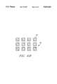
- the layered magnetic structure 40is then patterned and etched as shown in FIG. 5 to produce a planar dot an array 50 as of generally circular or rectangular dots 55 illustrated in FIG. 6A and 6B.
- the magnetic structureis etched down to the Surface of the silica layer 43 to form an array of magnetic dots 55 wherein each dot has the layered structure shown in FIG. 4.
- a conduction layer 57 of an electrically conductive materialis then deposited over the dot array filling in the spaces 59 between the dots 55 to provide electrical conductivity through the structure.
- the major dimension (diameter) of the dots 55is preferably 2.0 ⁇ m or less. While FIGS.
- the patterned dot array 50can be produced using well-known photolithography and etching techniques such as ion milling (RIE) or wet etching.
- RIEion milling
- FIGS. 7 and 8test samples comprising magnetic films having the multilayer structure, materials and dimensions as discussed above and having a 500 ⁇ overlayer 57 of tantalum (Ta) were prepared and the magnetoresistance measured.
- FIG. 7aplots the magnetoresistance versus applied magnetic field strength along both the magnetic hard and easy axes for a patterned film 50 wherein the overlayer of Ta served as the conduction layer.
- FIG. 7bis a plot of the magnetoresistance versus the applied magnetic field strength along both the magnetic hard and easy axes for an unpatterned film 40.
- the anisotropic MR effect (AMR)is the difference in the parallel and perpendicular curves 81 and 83, respectively.
- the giant MR effectis the average of the two curves 81, 83.
- the unpatterned film 40exhibits a predominantly AMR effect with a small GMR component.
- the patterned film 50exhibits a predominantly GMR effect with a small AMR component.
- the patterned filmexhibits little or no hysteresis while the unpatterned film exhibits substantial hysteresis along the easy axis.
- the measured magnitude of the MR effect in both the patterned and unpatterned test filmsis small because of current shunting from the Ta overlayer and poor electrical contact between the magnetic multilayer structure and the Ta overlayer.
- the magnitude of the AMR effectis about 0.2 to 0.4 percent.
- the AMR effectis approximately 7.6 percent of the GMR effect, which implies a GMR effect of 2.5 to 5.0 percent.
- the magnitude of the MR effect, deltaR/R, exhibited by the multilayer structureis largely determined by the choice of materials used in and the thickness of the magnetic and nonmagnetic layers.
- FIGS. 8a, 8b, 8c and 8dplot magnetization (M/M S ) versus the applied field strength (H) in the hard and easy axis direction for the patterned film 50 and the unpatterned film 40, respectively. Since the quantity of magnetic material measured in the test films was extremely small, a significant amount of background noise is observed with the measured date, especially with the patterned film 50.
- the unpatterned film 40exhibits a typical hard and easy axis hysteresis loop for a ferromagnetically coupled multilayer structure with an induced anisotropy field of about 3 Oe.
- the data for the dot array patterned film 50is characteristic of an antiferromagnetically ordered multilayer structure with an interaction field (equivalent to the saturation field) of approximately 20 Oe, which is consistent with the saturation field of the magnetoresistance curves shown in FIGS. 7a and 7b. Little or no hysteresis and a nearly linear dependence of M/M S on H, particularly along the hard axis, was observed for all of the patterned test films examined. The data shown by FIGS. 7a and 7 b suggest that the magnetic layers are single magnetic domains.
- dot arraysare not the only patterns that would be expected to exhibit the GMR effects discussed above.
- an antiferromagnetic magnetostatic interaction between magnetic layers in a multilayer structurewill occur whenever there is a discontinuity, or break, in the multilayer such that some component of the preferential direction of the magnetization (as determined by some anisotropy of the structure, such as shape, crystalline structure, surface feature or induced) is perpendicular to that discontinuity.
- Almost the only patterned structure that will not tend to order antiferromagneticallyis an elongated line structure with edges everywhere parallel and an easy axis along the length of the line, for example, the typical prior art MR stripe structure.
- the frequency and size of the discontinuitieswill determine the interaction field between layers. Complex multi-domain behavior may be exhibited in some structures. Other structures, such as an array 91 of holes or other apertures 93 formed in the multilayered film, as shown in FIG. 9a, or lines of modulated width such as the array 92 of connected or joined dots 94, as shown in FIG. 9b , are expected to provide simple, large-scale GMR devices that may find applications in addition to MR read heads used in magnetic recording systems.
- FIG. 10another preferred embodiment of the present invention is shown.
- the magnetoresistance of the structureis enhanced by the addition of a very thin layer of magnetic material at the interfaces between the magnetic layers 47, 51 and the spacer layer 51.
- a thin layer 46, 48 of cobalt (Co) formed at the interfaces between the NiFe layers 47, 51 and the spacer layer 49 of structure 40significantly increases the observed magnetoresistance of the structure
- magnetic layers 127, 131, 135, 139 of NiFe alternate with nonmagnetic spacer layers 129, 133, 137 of Ag with a cap layer 141 and an underlayer 125 of Taare formed on a surface layer 123 of SiO 2 over a suitable substrate 121 with a cap layer 141 and an underlayer 125 of Ta are formed on a surface layer 123 of SiO 2 over a suitable substrate 121 of Si.
- Any suitable ferromagnetic materialsuch as Fe, Ni, Co, or their alloys can be used for the magnetic layer material.
- any suitable nonmagnetic materialsuch as Au or Cu, for example, can be used for the nonmagnetic spacer layer material. As described above with reference to FIGS.
- arrays of dots or other suitable shapes having a major dimension of 10.0 ⁇ m or less, the maximum length being limited such that the net interaction between the layers is antiferromagnetic (as shown in FIG. 3, for example)are prepared using photolithographic and milling or etching techniques. Then a conduction layer (as shown in FIG. 5) is deposited over the dot array filling in the spaces between the dots in the array to provide electrical conductivity across the structure.
- Other patterned arrayssuch as described above with reference to FIGS. 9a and 9b, for example, are also suitable.
- a conduction layer 57is not required.
- only a capping layermay be required.
- the MR sensor 150comprises a magnetic bias layer 153 of a magnetic material, a nonmagnetic spacer layer 155 and multilayered MR sensor layer 157 deposited on a suitable substrate 151.
- the substrate 151may be glass, sapphire, quartz, magnesium oxide, silicon, silicon dioxide, Al 2 O 3 --TiC or other suitable material.
- An underlayer 152is first deposited over the substrate 153. The purpose of the underlayer 152 is to optimize the texture, grain size and morphology of the subsequently deposited magnetic layers 153 and 155. The underlayer 152 must have a high resistivity to minimize electrical current shunting effects.
- nonmagnetic, high resistivity materialssuch as tantalum (Ta), ruthenium (Ru) or aluminum oxide, for example, are suitable materials for the underlayer 152.
- the multilayer MR sensor layer 157comprises alternating magnetic and nonmagnetic layers which have been patterned in a dot array, for example, as described above with reference to FIGS. 4, 5, 10 and 11.
- the MR sensor layer 157will comprise a single generally square or rectangular dot element having the appropriate length and width as determined by the desired data track width and the requirement to provide an antiferromagnetic interaction field between the magnetic layers.
- the multilayered MR sensor layer 157preferably comprises 1-10 bilayers of magnetic and nonmagnetic material deposited over a base layer of magnetic material.
- the magnetic layersare of ferromagnetic material, preferably NiFe, but can be of any suitable ferromagnetic material such as Ni, Co, Fe and ferromagnetic alloys based on Ni, Fe or Co, for example.
- the spacer layerspreferably are of a nonmagnetic, metallic conductive material such as Au, Ag or Cu, for example, but can be of any nonmagnetic material having suitable conductivity or thin enough to allow transmission of conduction electrons.
- the bias layer 153provides a transverse magnetic bias field for the MR sensor layer 157 to provide a linear response for the sensor.
- the bias layermay be of a magnetically hard material (hard bias), such as CoPt or CoPtCr, for example, or of a magnetically soft material (soft bias), such as NiFe or NiFeRh, for example.
- hard biassuch as CoPt or CoPtCr
- soft biassuch as NiFe or NiFeRh
- the spacer layer 155serves to magnetically decouple the bias layer 153 from the MR sensing layer 157 and also to optimize the texture, grain size and morphology of the MR sensing layer.
- the spacer layer 155should be of a nonmagnetics, high resistivity material such as Ta, Zr, Ti, Y, Hf or other suitable material having the desired crystalline structure.
- a preferred embodiment of the MR sensor 150comprises a patterned multilayer MR sensor layer 157 of 5 bilayers of NiFe(20 ⁇ )/Ag(35 ⁇ ) on a base layer of NiFe(20 ⁇ ), a soft bias layer 153 of NiFe deposited on an underlayer 152 of Al 2 O 3 and separated from the MR sensor layer 157 by a spacer layer 155 of Ta having a thickness of approximately 50 ⁇ .
- the MR sensor 150is deposited on a ceramic substrate 151 by sputter deposition or other suitable deposition process as is known in the art.
- the thickness of the underlayer 152preferably is in the range of 100 to 500 ⁇ .
- the NiFe soft bias layer 153 thicknessis in the range of 50-300 ⁇ , preferably 100 ⁇ .
- Conductor terminals 161 of Cu or other suitable material, such as Ta, Ag or Au, formed at opposite ends of the MR sensor 150connect the MR sensor to current source 163 and signal sensing circuitry 165 via lead conductors 167.
- the current source 163provides a sense current to the MR sensor 150 which senses the changes in resistance of the MR sensor element 157 when an external magnetic field is applied.
- a capping layer 159 of a high resistivity material such as Ta or Zr, for example,can also be deposited over the MR sensor layer 157.
Landscapes
- Engineering & Computer Science (AREA)
- Chemical & Material Sciences (AREA)
- Nanotechnology (AREA)
- Physics & Mathematics (AREA)
- Crystallography & Structural Chemistry (AREA)
- General Physics & Mathematics (AREA)
- Condensed Matter Physics & Semiconductors (AREA)
- Mathematical Physics (AREA)
- Theoretical Computer Science (AREA)
- Manufacturing & Machinery (AREA)
- Hall/Mr Elements (AREA)
- Measuring Magnetic Variables (AREA)
- Magnetic Heads (AREA)
- Thin Magnetic Films (AREA)
Abstract
Description
Claims (89)
Priority Applications (13)
| Application Number | Priority Date | Filing Date | Title |
|---|---|---|---|
| US08/173,590US5452163A (en) | 1993-12-23 | 1993-12-23 | Multilayer magnetoresistive sensor |
| TW083108817ATW277132B (en) | 1993-12-23 | 1994-09-23 | |
| CA002134711ACA2134711A1 (en) | 1993-12-23 | 1994-10-31 | Multilayer magnetoresistive sensor |
| JP6269414AJP2784461B2 (en) | 1993-12-23 | 1994-11-02 | Multilayer magnetoresistive sensor and magnetic storage system |
| CN94118724ACN1068689C (en) | 1993-12-23 | 1994-11-19 | Multilayer magnetoresistive sensor |
| MYPI94003100AMY116219A (en) | 1993-12-23 | 1994-11-21 | Multilayer magnetoresistive sensor. |
| KR1019940030840AKR0146012B1 (en) | 1993-12-23 | 1994-11-23 | Multilayer magnetoresistive sensor |
| PH49556APH30835A (en) | 1993-12-23 | 1994-12-14 | Multilayer magnetoresistive sensor. |
| DE69431149TDE69431149T2 (en) | 1993-12-23 | 1994-12-16 | Magnetoresistive sensor in multi-layer construction |
| SG1996000132ASG42849A1 (en) | 1993-12-23 | 1994-12-16 | Multilayer magnetoresistive sensor |
| AT94119895TATE221999T1 (en) | 1993-12-23 | 1994-12-16 | MAGNETORESISTIC SENSOR IN MULTI-LAYER CONSTRUCTION |
| EP94119895AEP0660127B1 (en) | 1993-12-23 | 1994-12-16 | Multilayer magnetoresistive sensor |
| BR9405159ABR9405159A (en) | 1993-12-23 | 1994-12-20 | Multilayer magnetoresistive sensor, method of manufacturing it and magnetic storage system that uses it |
Applications Claiming Priority (1)
| Application Number | Priority Date | Filing Date | Title |
|---|---|---|---|
| US08/173,590US5452163A (en) | 1993-12-23 | 1993-12-23 | Multilayer magnetoresistive sensor |
Publications (1)
| Publication Number | Publication Date |
|---|---|
| US5452163Atrue US5452163A (en) | 1995-09-19 |
Family
ID=22632713
Family Applications (1)
| Application Number | Title | Priority Date | Filing Date |
|---|---|---|---|
| US08/173,590Expired - LifetimeUS5452163A (en) | 1993-12-23 | 1993-12-23 | Multilayer magnetoresistive sensor |
Country Status (13)
| Country | Link |
|---|---|
| US (1) | US5452163A (en) |
| EP (1) | EP0660127B1 (en) |
| JP (1) | JP2784461B2 (en) |
| KR (1) | KR0146012B1 (en) |
| CN (1) | CN1068689C (en) |
| AT (1) | ATE221999T1 (en) |
| BR (1) | BR9405159A (en) |
| CA (1) | CA2134711A1 (en) |
| DE (1) | DE69431149T2 (en) |
| MY (1) | MY116219A (en) |
| PH (1) | PH30835A (en) |
| SG (1) | SG42849A1 (en) |
| TW (1) | TW277132B (en) |
Cited By (59)
| Publication number | Priority date | Publication date | Assignee | Title |
|---|---|---|---|---|
| US5563331A (en)* | 1993-09-29 | 1996-10-08 | Siemens Aktiengesellschaft | Magnetoresistive sensor utilizing a sensor material with a perovskite-like crystal structure |
| US5585986A (en)* | 1995-05-15 | 1996-12-17 | International Business Machines Corporation | Digital magnetoresistive sensor based on the giant magnetoresistance effect |
| US5627703A (en)* | 1994-03-09 | 1997-05-06 | Eastman Kodak Company | Dual magnetoresistive reproduce head utilizing multilayer magnetoresistive sensing elements |
| US5635835A (en)* | 1994-07-21 | 1997-06-03 | Commissariat A L'energie Atomique | Self biased multilayer magnetoresistance sensor |
| US5636093A (en)* | 1994-10-05 | 1997-06-03 | U.S. Philips Corporation | Magnetic multilayer device having resonant-tunneling double-barrier structure |
| US5641557A (en)* | 1994-08-29 | 1997-06-24 | Nec Corporation | Magnetoresistive element |
| US5652445A (en)* | 1995-04-21 | 1997-07-29 | Johnson; Mark B. | Hybrid hall effect device and method of operation |
| US5657190A (en)* | 1993-03-02 | 1997-08-12 | Tdk Corporation | Apparatus for detecting a magnetic field using a giant magnetoresistance effect multilayer |
| US5661621A (en)* | 1994-09-08 | 1997-08-26 | Fujitsu Limited | Magnetoresistive head |
| US5666248A (en)* | 1996-09-13 | 1997-09-09 | International Business Machines Corporation | Magnetizations of pinned and free layers of a spin valve sensor set by sense current fields |
| US5701222A (en)* | 1995-09-11 | 1997-12-23 | International Business Machines Corporation | Spin valve sensor with antiparallel magnetization of pinned layers |
| US5737157A (en)* | 1996-10-09 | 1998-04-07 | International Business Machines Corporation | Disk drive with a thermal asperity reduction circuitry using a magnetoresistive sensor |
| US5739987A (en)* | 1996-06-04 | 1998-04-14 | Read-Rite Corporation | Magnetoresistive read transducers with multiple longitudinal stabilization layers |
| US5747997A (en)* | 1996-06-05 | 1998-05-05 | Regents Of The University Of Minnesota | Spin-valve magnetoresistance sensor having minimal hysteresis problems |
| US5773156A (en)* | 1995-01-26 | 1998-06-30 | Kabushiki Kaisha Toshiba | Magnetoresistance effect element |
| US5793279A (en)* | 1996-08-26 | 1998-08-11 | Read-Rite Corporation | Methods and compositions for optimizing interfacial properties of magnetoresistive sensors |
| WO1998038792A1 (en)* | 1997-02-28 | 1998-09-03 | University And Community College System Of Nevada | Magnetoresistive scanning system |
| US5858508A (en)* | 1994-07-28 | 1999-01-12 | Custom Plastics Molding, Inc. | Method of forming antislip surfaces on thermoformed products |
| US5867351A (en)* | 1997-07-25 | 1999-02-02 | International Business Machines Corporation | Spin valve read head with low moment, high coercivity pinning layer |
| US5874886A (en)* | 1994-07-06 | 1999-02-23 | Tdk Corporation | Magnetoresistance effect element and magnetoresistance device |
| US5923505A (en)* | 1997-03-17 | 1999-07-13 | Read-Rite Corporation | Magnetoresistive sensor having a pinned soft magnetic layer |
| US5932097A (en)* | 1997-12-01 | 1999-08-03 | International Business Machines Corporation | Microfabricated magnetic particles for applications to affinity binding |
| US5966275A (en)* | 1997-09-18 | 1999-10-12 | Fujitsu Limited | GMR magnetic sensor having an improved sensitivity of magnetic detection |
| US6002553A (en)* | 1994-02-28 | 1999-12-14 | The United States Of America As Represented By The United States Department Of Energy | Giant magnetoresistive sensor |
| US6021065A (en)* | 1996-09-06 | 2000-02-01 | Nonvolatile Electronics Incorporated | Spin dependent tunneling memory |
| US6064083A (en)* | 1995-04-21 | 2000-05-16 | Johnson; Mark B. | Hybrid hall effect memory device and method of operation |
| US6140838A (en)* | 1995-04-21 | 2000-10-31 | Johnson; Mark B. | High density and high speed magneto-electronic logic family |
| US6147900A (en)* | 1997-11-06 | 2000-11-14 | Nonvolatile Electronics, Incorporated | Spin dependent tunneling memory |
| US6147843A (en)* | 1996-01-26 | 2000-11-14 | Nec Corporation | Magnetoresistive effect element having magnetoresistive layer and underlying metal layer |
| US6157523A (en)* | 1994-12-21 | 2000-12-05 | Fujitsu Limited | Spin valve magnetoresistive head having magnetic layers with different internal stress |
| US6166539A (en)* | 1996-10-30 | 2000-12-26 | Regents Of The University Of Minnesota | Magnetoresistance sensor having minimal hysteresis problems |
| US6169687B1 (en) | 1995-04-21 | 2001-01-02 | Mark B. Johnson | High density and speed magneto-electronic memory for use in computing system |
| US6171676B1 (en) | 1996-03-19 | 2001-01-09 | Fujitsu Limited | Magnetic recording medium containing fine magnetic crystal grains and its manufacture |
| US6191495B1 (en)* | 1997-06-10 | 2001-02-20 | Lucent Technologies Inc. | Micromagnetic device having an anisotropic ferromagnetic core and method of manufacture therefor |
| US6221559B1 (en) | 1996-10-21 | 2001-04-24 | International Business Machines Corporation | Method of making crack resistant magnetic write head |
| US6275411B1 (en) | 1993-07-23 | 2001-08-14 | Nonvolatile Electronics, Incorporated | Spin dependent tunneling memory |
| US6307774B1 (en) | 2000-03-22 | 2001-10-23 | Mark B. Johnson | Magnetoelectronic memory array |
| US20020034056A1 (en)* | 2000-09-19 | 2002-03-21 | Lujun Chen | Giant magnetoresistive sensor having selfconsistent demagnetization fields |
| US6404601B1 (en) | 2000-01-25 | 2002-06-11 | Read-Rite Corporation | Merged write head with magnetically isolated poletip |
| US20020145832A1 (en)* | 2001-04-04 | 2002-10-10 | Seagate Technology Llc | Perpendicular magnetic recording head with soft underlayer biasing |
| US6486662B1 (en)* | 1997-10-29 | 2002-11-26 | Koninklijke Philips Electronics N.V. | Magnetic field sensor comprising a spin-tunnel junction |
| US20020181167A1 (en)* | 1995-03-31 | 2002-12-05 | Gambino Richard Joseph | Magnetoresistive sensor with magnetostatic coupling of magnetic regions |
| US6600637B1 (en)* | 1999-10-28 | 2003-07-29 | Seagate Technology, L.L.C. | Edge barrier to prevent spin valve sensor corrosion and improve long term reliability |
| US20030141957A1 (en)* | 1998-05-27 | 2003-07-31 | Bohlinger Michael J. | Magnetic field sensing device |
| US6649422B2 (en) | 1999-06-22 | 2003-11-18 | Agere Systems Inc. | Integrated circuit having a micromagnetic device and method of manufacture therefor |
| US6696744B2 (en) | 1997-06-10 | 2004-02-24 | Agere Systems, Inc. | Integrated circuit having a micromagnetic device and method of manufacture therefor |
| US6709767B2 (en) | 2001-07-31 | 2004-03-23 | Hitachi Global Storage Technologies Netherlands B.V. | In-situ oxidized films for use as cap and gap layers in a spin-valve sensor and methods of manufacture |
| US6724586B2 (en)* | 2001-03-27 | 2004-04-20 | Hitachi Global Storage Technologies Netherlands B.V. | Bias structure for magnetic tunnel junction magnetoresistive sensor |
| US6741494B2 (en) | 1995-04-21 | 2004-05-25 | Mark B. Johnson | Magnetoelectronic memory element with inductively coupled write wires |
| US20050013060A1 (en)* | 2003-07-14 | 2005-01-20 | International Business Machines Corporation | Magnetoresistive sensor |
| US20050018345A1 (en)* | 2001-05-08 | 2005-01-27 | Ramot At Tel-Aviv University Ltd. | Magnetic thin film sensor based on the extraordinary hall effect |
| US20050057986A1 (en)* | 1995-04-21 | 2005-03-17 | Johnson Mark B. | Magnetic spin based memory with inductive write lines |
| US20050094323A1 (en)* | 2000-10-26 | 2005-05-05 | Headway Technologies, Inc. | Integrated spin valve head |
| US20050099738A1 (en)* | 2003-11-06 | 2005-05-12 | Seagate Technology Llc | Magnetoresistive sensor having specular sidewall layers |
| US20090224342A1 (en)* | 2007-10-12 | 2009-09-10 | Masahiko Nakayama | Magnetoresistive effect element and magnetic random access memory |
| US20100020447A1 (en)* | 2008-07-24 | 2010-01-28 | Infineon Technologies Ag | System with 90 degree sense layer magnetic orientation |
| US8995073B1 (en)* | 2013-03-14 | 2015-03-31 | Seagate Technology Llc | Data storage mediums and devices having bit patterned media |
| EP3646046B1 (en)* | 2017-06-28 | 2023-02-15 | Centre National De La Recherche Scientifique | Device for measuring weak magnetic fields |
| US11719772B2 (en) | 2020-04-01 | 2023-08-08 | Analog Devices International Unlimited Company | AMR (XMR) sensor with increased linear range |
Families Citing this family (15)
| Publication number | Priority date | Publication date | Assignee | Title |
|---|---|---|---|---|
| US6239595B1 (en)* | 1998-05-13 | 2001-05-29 | Mitsubishi Denki Kabushiki Kaisha | Magnetic field sensing element |
| JP3544141B2 (en) | 1998-05-13 | 2004-07-21 | 三菱電機株式会社 | Magnetic detecting element and magnetic detecting device |
| DE19854713B4 (en)* | 1998-05-13 | 2005-03-10 | Mitsubishi Electric Corp | Magnetic field sensing element |
| DE19843349A1 (en)* | 1998-09-22 | 2000-03-23 | Bosch Gmbh Robert | Magneto-resistive sensor element for measurement of external magnetic field angle, especially in bridge circuits, has outer sensor layer comprised partially or completely of individual segments |
| US6178074B1 (en)* | 1998-11-19 | 2001-01-23 | International Business Machines Corporation | Double tunnel junction with magnetoresistance enhancement layer |
| US6421212B1 (en) | 1999-09-21 | 2002-07-16 | Read-Rite Corporation | Thin film read head structure with improved bias magnet-to-magnetoresistive element interface and method of fabrication |
| DE10258860A1 (en)* | 2002-12-17 | 2004-07-15 | Robert Bosch Gmbh | Magnetoresistive layer system and sensor element with this layer system |
| US7286392B2 (en)* | 2003-11-24 | 2007-10-23 | Nxp B.V. | Data retention indicator for magnetic memories |
| US8907666B2 (en)* | 2011-09-30 | 2014-12-09 | HGST Netherlands B.V. | Magnetic bias structure for magnetoresistive sensor having a scissor structure |
| CN104900800A (en)* | 2014-03-03 | 2015-09-09 | 北京嘉岳同乐极电子有限公司 | GMR magnetic nanometer multilayer film used for magneto-dependent sensor |
| US10483320B2 (en) | 2015-12-10 | 2019-11-19 | Everspin Technologies, Inc. | Magnetoresistive stack with seed region and method of manufacturing the same |
| EP4181656A1 (en)* | 2018-11-19 | 2023-05-17 | Everspin Technologies, Inc. | Magnetoresistive stack with seed region and method of manufacturing the same |
| CN115265605B (en)* | 2021-12-01 | 2024-03-12 | 苏州纳芯微电子股份有限公司 | Sensor circuit and motion data detection device |
| CN115077571A (en)* | 2021-12-09 | 2022-09-20 | 苏州纳芯微电子股份有限公司 | Motion data detection device and sensor circuit thereof |
| CN118519081A (en)* | 2024-05-30 | 2024-08-20 | 珠海多创科技有限公司 | Magneto-resistive element, magnetic switch sensor and electronic equipment |
Citations (7)
| Publication number | Priority date | Publication date | Assignee | Title |
|---|---|---|---|---|
| US4896235A (en)* | 1985-11-05 | 1990-01-23 | Sony Corporation | Magnetic transducer head utilizing magnetoresistance effect |
| US4914538A (en)* | 1988-08-18 | 1990-04-03 | International Business Machines Corporation | Magnetoresistive read transducer |
| US4949039A (en)* | 1988-06-16 | 1990-08-14 | Kernforschungsanlage Julich Gmbh | Magnetic field sensor with ferromagnetic thin layers having magnetically antiparallel polarized components |
| US5206590A (en)* | 1990-12-11 | 1993-04-27 | International Business Machines Corporation | Magnetoresistive sensor based on the spin valve effect |
| US5327313A (en)* | 1991-08-01 | 1994-07-05 | Hitachi, Ltd. | Magnetoresistance effect type head having a damage immune film structure |
| US5337203A (en)* | 1988-02-26 | 1994-08-09 | Hitachi, Ltd. | Magnetoresistive magnetic head |
| US5343422A (en)* | 1993-02-23 | 1994-08-30 | International Business Machines Corporation | Nonvolatile magnetoresistive storage device using spin valve effect |
Family Cites Families (4)
| Publication number | Priority date | Publication date | Assignee | Title |
|---|---|---|---|---|
| US134533A (en)* | 1873-01-07 | Improvement in spring motive powers | ||
| FR2648942B1 (en)* | 1989-06-27 | 1995-08-11 | Thomson Csf | SENSOR WITH MAGNETORESISTIVE EFFECT |
| US5032945A (en)* | 1989-11-07 | 1991-07-16 | International Business Machines Corp. | Magnetic thin film structures fabricated with edge closure layers |
| FR2693021B1 (en)* | 1992-06-26 | 1994-08-26 | Thomson Csf | Magnetic field detector. |
- 1993
- 1993-12-23USUS08/173,590patent/US5452163A/ennot_activeExpired - Lifetime
- 1994
- 1994-09-23TWTW083108817Apatent/TW277132B/zhactive
- 1994-10-31CACA002134711Apatent/CA2134711A1/ennot_activeAbandoned
- 1994-11-02JPJP6269414Apatent/JP2784461B2/ennot_activeExpired - Fee Related
- 1994-11-19CNCN94118724Apatent/CN1068689C/ennot_activeExpired - Fee Related
- 1994-11-21MYMYPI94003100Apatent/MY116219A/enunknown
- 1994-11-23KRKR1019940030840Apatent/KR0146012B1/ennot_activeExpired - Fee Related
- 1994-12-14PHPH49556Apatent/PH30835A/enunknown
- 1994-12-16DEDE69431149Tpatent/DE69431149T2/ennot_activeExpired - Fee Related
- 1994-12-16EPEP94119895Apatent/EP0660127B1/ennot_activeExpired - Lifetime
- 1994-12-16ATAT94119895Tpatent/ATE221999T1/ennot_activeIP Right Cessation
- 1994-12-16SGSG1996000132Apatent/SG42849A1/enunknown
- 1994-12-20BRBR9405159Apatent/BR9405159A/ennot_activeApplication Discontinuation
Patent Citations (7)
| Publication number | Priority date | Publication date | Assignee | Title |
|---|---|---|---|---|
| US4896235A (en)* | 1985-11-05 | 1990-01-23 | Sony Corporation | Magnetic transducer head utilizing magnetoresistance effect |
| US5337203A (en)* | 1988-02-26 | 1994-08-09 | Hitachi, Ltd. | Magnetoresistive magnetic head |
| US4949039A (en)* | 1988-06-16 | 1990-08-14 | Kernforschungsanlage Julich Gmbh | Magnetic field sensor with ferromagnetic thin layers having magnetically antiparallel polarized components |
| US4914538A (en)* | 1988-08-18 | 1990-04-03 | International Business Machines Corporation | Magnetoresistive read transducer |
| US5206590A (en)* | 1990-12-11 | 1993-04-27 | International Business Machines Corporation | Magnetoresistive sensor based on the spin valve effect |
| US5327313A (en)* | 1991-08-01 | 1994-07-05 | Hitachi, Ltd. | Magnetoresistance effect type head having a damage immune film structure |
| US5343422A (en)* | 1993-02-23 | 1994-08-30 | International Business Machines Corporation | Nonvolatile magnetoresistive storage device using spin valve effect |
Non-Patent Citations (12)
| Title |
|---|
| A. Berkowitz et al., "Giant Magnetoresistance in Heterogeneous Cu-Co Alloys", Physical Review Letters, vol. 68, No. 25, Jun. 1992, pp. 3745-3748. |
| A. Berkowitz et al., Giant Magnetoresistance in Heterogeneous Cu Co Alloys , Physical Review Letters, vol. 68, No. 25, Jun. 1992, pp. 3745 3748.* |
| B. Dieny et al., "Giant magnetoresistance in soft ferromagnetic multilayers", Physical Review B. vol. 43, No. 1, Jan. 1991, pp. 1297-1300. |
| B. Dieny et al., Giant magnetoresistance in soft ferromagnetic multilayers , Physical Review B. vol. 43, No. 1, Jan. 1991, pp. 1297 1300.* |
| G. Binasch et al., "Enhanced magnetoresistance in layered magnetic structures with antiferromagnetic interlayer exchange", Physical Review B, vol. 39, No. 7, Mar. 1989, pp. 4828-4830. |
| G. Binasch et al., Enhanced magnetoresistance in layered magnetic structures with antiferromagnetic interlayer exchange , Physical Review B, vol. 39, No. 7, Mar. 1989, pp. 4828 4830.* |
| J. Slonczewski et al., "Micromagnetics of Laminated Permalloy Films", IEEE Trans. on Magnetics, vol. 24, No. 3, May 1988, pp. 2045-2054. |
| J. Slonczewski et al., Micromagnetics of Laminated Permalloy Films , IEEE Trans. on Magnetics, vol. 24, No. 3, May 1988, pp. 2045 2054.* |
| J. Ziao et al., "Giant Magnetoresistance in Nonmultilayer Magnetic Systems", Physical Review Letters, vol. 68, No. 25, Jun. 1993, pp. 3749-3752. |
| J. Ziao et al., Giant Magnetoresistance in Nonmultilayer Magnetic Systems , Physical Review Letters, vol. 68, No. 25, Jun. 1993, pp. 3749 3752.* |
| M. Baibich et al., "Giant Magnetoresistance of (001)Fe/(001)Cr Magnetic Superlattices", Physical Review Letters, vol. 61, No. 21, Nov. 1988, pp. 2472-2475. |
| M. Baibich et al., Giant Magnetoresistance of (001)Fe/(001)Cr Magnetic Superlattices , Physical Review Letters, vol. 61, No. 21, Nov. 1988, pp. 2472 2475.* |
Cited By (128)
| Publication number | Priority date | Publication date | Assignee | Title |
|---|---|---|---|---|
| US5798896A (en)* | 1993-03-02 | 1998-08-25 | Tdk Corporation | Apparatus for detecting a magnetic field using a giant magnetoresistance effect multilayer and method for preventing an output reduction of the multilayer |
| US5657190A (en)* | 1993-03-02 | 1997-08-12 | Tdk Corporation | Apparatus for detecting a magnetic field using a giant magnetoresistance effect multilayer |
| US6275411B1 (en) | 1993-07-23 | 2001-08-14 | Nonvolatile Electronics, Incorporated | Spin dependent tunneling memory |
| US5563331A (en)* | 1993-09-29 | 1996-10-08 | Siemens Aktiengesellschaft | Magnetoresistive sensor utilizing a sensor material with a perovskite-like crystal structure |
| US6002553A (en)* | 1994-02-28 | 1999-12-14 | The United States Of America As Represented By The United States Department Of Energy | Giant magnetoresistive sensor |
| US5627703A (en)* | 1994-03-09 | 1997-05-06 | Eastman Kodak Company | Dual magnetoresistive reproduce head utilizing multilayer magnetoresistive sensing elements |
| US5874886A (en)* | 1994-07-06 | 1999-02-23 | Tdk Corporation | Magnetoresistance effect element and magnetoresistance device |
| US6074743A (en)* | 1994-07-06 | 2000-06-13 | Tdk Corporation | Magnetoresistance effect element and magnetoresistance device |
| US5635835A (en)* | 1994-07-21 | 1997-06-03 | Commissariat A L'energie Atomique | Self biased multilayer magnetoresistance sensor |
| US5858508A (en)* | 1994-07-28 | 1999-01-12 | Custom Plastics Molding, Inc. | Method of forming antislip surfaces on thermoformed products |
| US5876843A (en)* | 1994-08-29 | 1999-03-02 | Nec Corporation | Magnetoresistive element |
| US5641557A (en)* | 1994-08-29 | 1997-06-24 | Nec Corporation | Magnetoresistive element |
| US5661621A (en)* | 1994-09-08 | 1997-08-26 | Fujitsu Limited | Magnetoresistive head |
| US5636093A (en)* | 1994-10-05 | 1997-06-03 | U.S. Philips Corporation | Magnetic multilayer device having resonant-tunneling double-barrier structure |
| US6157523A (en)* | 1994-12-21 | 2000-12-05 | Fujitsu Limited | Spin valve magnetoresistive head having magnetic layers with different internal stress |
| US5773156A (en)* | 1995-01-26 | 1998-06-30 | Kabushiki Kaisha Toshiba | Magnetoresistance effect element |
| US20020181167A1 (en)* | 1995-03-31 | 2002-12-05 | Gambino Richard Joseph | Magnetoresistive sensor with magnetostatic coupling of magnetic regions |
| US6510031B1 (en)* | 1995-03-31 | 2003-01-21 | International Business Machines Corporation | Magnetoresistive sensor with magnetostatic coupling to obtain opposite alignment of magnetic regions |
| US6775109B2 (en)* | 1995-03-31 | 2004-08-10 | International Business Machines Corporation | Magnetoresistive sensor with magnetostatic coupling of magnetic regions |
| US20040196595A1 (en)* | 1995-03-31 | 2004-10-07 | Gambino Richard Joseph | Magnetoresistive sensor with magnetostatic coupling of magnetic regions |
| US6914761B2 (en)* | 1995-03-31 | 2005-07-05 | International Business Machines Corporation | Magnetoresistive sensor with magnetic flux paths surrounding non-magnetic regions of ferromagnetic material layer |
| US7068535B2 (en) | 1995-04-21 | 2006-06-27 | Johnson Mark B | Magnetic spin based memory with semiconductor selector |
| US20060158927A1 (en)* | 1995-04-21 | 2006-07-20 | Johnson Mark B | Spin based electronic device |
| US7596018B2 (en) | 1995-04-21 | 2009-09-29 | Seagate Technology Int'l | Spin memory with write pulse |
| US7570510B2 (en) | 1995-04-21 | 2009-08-04 | Seagate Technology International | Multi-bit spin memory |
| US7339819B2 (en) | 1995-04-21 | 2008-03-04 | Seagate Technology Llc | Spin based memory coupled to CMOS amplifier |
| US20080049492A1 (en)* | 1995-04-21 | 2008-02-28 | Johnson Mark B | Spin Memory with Write Pulse |
| US20080049489A1 (en)* | 1995-04-21 | 2008-02-28 | Johnson Mark B | Multi-Bit Spin Memory |
| US7309888B2 (en) | 1995-04-21 | 2007-12-18 | Seagate Technology Llc | Spin based electronic device |
| US6064083A (en)* | 1995-04-21 | 2000-05-16 | Johnson; Mark B. | Hybrid hall effect memory device and method of operation |
| US7307875B2 (en) | 1995-04-21 | 2007-12-11 | Seagate Technology Llc | Spin based magnetic sensor |
| US20070206407A1 (en)* | 1995-04-21 | 2007-09-06 | Johnson Mark B | Spin Based Memory Coupled to CMOS Amplifier |
| US6140838A (en)* | 1995-04-21 | 2000-10-31 | Johnson; Mark B. | High density and high speed magneto-electronic logic family |
| US20070201268A1 (en)* | 1995-04-21 | 2007-08-30 | Johnson Mark B | Spin Based Magnetic Sensor |
| US7215570B2 (en) | 1995-04-21 | 2007-05-08 | Spinop Corporation | Spin based device with low transmission barrier |
| US7212433B2 (en) | 1995-04-21 | 2007-05-01 | Spinop Corporation | Ferromagnetic layer compositions and structures for spin polarized memory devices, including memory devices |
| US7209381B2 (en) | 1995-04-21 | 2007-04-24 | Spinop Corporation | Digital processing device with disparate magnetoelectronic gates |
| US6169687B1 (en) | 1995-04-21 | 2001-01-02 | Mark B. Johnson | High density and speed magneto-electronic memory for use in computing system |
| US7193891B2 (en) | 1995-04-21 | 2007-03-20 | Spinop Corporation | Spin based sensor device |
| US20060187704A1 (en)* | 1995-04-21 | 2006-08-24 | Johnson Mark B | Spin based sensor device |
| US20060152968A1 (en)* | 1995-04-21 | 2006-07-13 | Johnson Mark B | Spin based device with low transmission barrier |
| US7064976B2 (en) | 1995-04-21 | 2006-06-20 | Spin Op Corporation | Method of operating a stacked spin based memory |
| US6288565B1 (en) | 1995-04-21 | 2001-09-11 | Mark B. Johnson | High density and high speed magneto-electronic logic family |
| US7050329B2 (en) | 1995-04-21 | 2006-05-23 | Johnson Mark B | Magnetic spin based memory with inductive write lines |
| US7020013B2 (en) | 1995-04-21 | 2006-03-28 | Johnson Mark B | Magnetic field sensor using spin polarized current |
| US6342713B1 (en) | 1995-04-21 | 2002-01-29 | Mark B. Johnson | Method of operating a magnetoelectronic device |
| US7016223B2 (en) | 1995-04-21 | 2006-03-21 | Johnson Mark B | Magnetoelectronic memory element with inductively coupled write wires |
| US7009875B2 (en) | 1995-04-21 | 2006-03-07 | Johnson Mark B | Magnetic memory device structure |
| US6388916B1 (en) | 1995-04-21 | 2002-05-14 | Mark B. Johnson | Magnetoelectronic memory element with isolation element |
| US6975533B2 (en) | 1995-04-21 | 2005-12-13 | Johnson Mark B | Hybrid semiconductor—magnetic spin based memory with low transmission barrier |
| US6423553B1 (en) | 1995-04-21 | 2002-07-23 | Mark B. Johnson | Method of making a magnetoelectronic device |
| US20050237792A1 (en)* | 1995-04-21 | 2005-10-27 | Johnson Mark B | Magnetic memory device structure |
| US6958930B2 (en) | 1995-04-21 | 2005-10-25 | Johnson Mark B | Magnetoelectronic device with variable magnetic write field |
| US20050207240A1 (en)* | 1995-04-21 | 2005-09-22 | Johnson Mark B | Digital processing device with disparate magnetoelectronic gates |
| US20050190593A1 (en)* | 1995-04-21 | 2005-09-01 | Johnson Mark B. | Magnetoelectronic memory element with inductively coupled write wires |
| US20050169047A1 (en)* | 1995-04-21 | 2005-08-04 | Johnson Mark B. | Magnetic field sensor using spin polarized current |
| US20050162903A1 (en)* | 1995-04-21 | 2005-07-28 | Johnson Mark B. | Method of operating a stacked spin based memory |
| US5652445A (en)* | 1995-04-21 | 1997-07-29 | Johnson; Mark B. | Hybrid hall effect device and method of operation |
| US6888746B2 (en) | 1995-04-21 | 2005-05-03 | Mark B. Johnson | Magnetoelectronic memory element with inductively coupled write wires |
| US20050088884A1 (en)* | 1995-04-21 | 2005-04-28 | Johnson Mark B. | Hybrid semiconductor - magnetic spin based memory with low transmission barrier |
| US6873545B2 (en) | 1995-04-21 | 2005-03-29 | Mark B. Johnson | Hybrid semiconductor-magnetic device and method of operation |
| US20050063239A1 (en)* | 1995-04-21 | 2005-03-24 | Johnson Mark B. | Magnetic spin based memory with semiconductor selector |
| US6741494B2 (en) | 1995-04-21 | 2004-05-25 | Mark B. Johnson | Magnetoelectronic memory element with inductively coupled write wires |
| US6870761B2 (en) | 1995-04-21 | 2005-03-22 | Mark B. Johnson | Stacked hybrid semiconductor-magnetic spin based memory |
| US20040160800A1 (en)* | 1995-04-21 | 2004-08-19 | Johnson Mark B. | Stacked hybrid semiconductor-magnetic spin based memory |
| US20050057986A1 (en)* | 1995-04-21 | 2005-03-17 | Johnson Mark B. | Magnetic spin based memory with inductive write lines |
| US20050047204A1 (en)* | 1995-04-21 | 2005-03-03 | Johnson Mark B. | Ferromagnetic layer compositions and structures for spin polarized memory device |
| US20040213042A1 (en)* | 1995-04-21 | 2004-10-28 | Johnson Mark B. | Magnetoelectronic device with variable magnetic write field |
| US20040213041A1 (en)* | 1995-04-21 | 2004-10-28 | Johnson Mark B. | Magnetoelectronic memory element with inductively coupled write wires |
| US5585986A (en)* | 1995-05-15 | 1996-12-17 | International Business Machines Corporation | Digital magnetoresistive sensor based on the giant magnetoresistance effect |
| US6055136A (en)* | 1995-09-11 | 2000-04-25 | International Business Machines Corporation | Spin valve sensor with antiparallel magnetization of pinned layers |
| US5701222A (en)* | 1995-09-11 | 1997-12-23 | International Business Machines Corporation | Spin valve sensor with antiparallel magnetization of pinned layers |
| US6147843A (en)* | 1996-01-26 | 2000-11-14 | Nec Corporation | Magnetoresistive effect element having magnetoresistive layer and underlying metal layer |
| US6171676B1 (en) | 1996-03-19 | 2001-01-09 | Fujitsu Limited | Magnetic recording medium containing fine magnetic crystal grains and its manufacture |
| US5739987A (en)* | 1996-06-04 | 1998-04-14 | Read-Rite Corporation | Magnetoresistive read transducers with multiple longitudinal stabilization layers |
| US5747997A (en)* | 1996-06-05 | 1998-05-05 | Regents Of The University Of Minnesota | Spin-valve magnetoresistance sensor having minimal hysteresis problems |
| US5793279A (en)* | 1996-08-26 | 1998-08-11 | Read-Rite Corporation | Methods and compositions for optimizing interfacial properties of magnetoresistive sensors |
| US6021065A (en)* | 1996-09-06 | 2000-02-01 | Nonvolatile Electronics Incorporated | Spin dependent tunneling memory |
| US5666248A (en)* | 1996-09-13 | 1997-09-09 | International Business Machines Corporation | Magnetizations of pinned and free layers of a spin valve sensor set by sense current fields |
| US5793576A (en)* | 1996-10-09 | 1998-08-11 | International Business Machines Corporation | Disk drive with a thermal asperity reduction circuitry using a magnetoresis sensor |
| US5737157A (en)* | 1996-10-09 | 1998-04-07 | International Business Machines Corporation | Disk drive with a thermal asperity reduction circuitry using a magnetoresistive sensor |
| US6221559B1 (en) | 1996-10-21 | 2001-04-24 | International Business Machines Corporation | Method of making crack resistant magnetic write head |
| US6166539A (en)* | 1996-10-30 | 2000-12-26 | Regents Of The University Of Minnesota | Magnetoresistance sensor having minimal hysteresis problems |
| WO1998038792A1 (en)* | 1997-02-28 | 1998-09-03 | University And Community College System Of Nevada | Magnetoresistive scanning system |
| US5923505A (en)* | 1997-03-17 | 1999-07-13 | Read-Rite Corporation | Magnetoresistive sensor having a pinned soft magnetic layer |
| US6191495B1 (en)* | 1997-06-10 | 2001-02-20 | Lucent Technologies Inc. | Micromagnetic device having an anisotropic ferromagnetic core and method of manufacture therefor |
| US6696744B2 (en) | 1997-06-10 | 2004-02-24 | Agere Systems, Inc. | Integrated circuit having a micromagnetic device and method of manufacture therefor |
| US5867351A (en)* | 1997-07-25 | 1999-02-02 | International Business Machines Corporation | Spin valve read head with low moment, high coercivity pinning layer |
| US6105237A (en)* | 1997-07-25 | 2000-08-22 | International Business Machines Corporation | Method of making spin value read head with low moment, high coercivity pinning layer |
| US5966275A (en)* | 1997-09-18 | 1999-10-12 | Fujitsu Limited | GMR magnetic sensor having an improved sensitivity of magnetic detection |
| US6486662B1 (en)* | 1997-10-29 | 2002-11-26 | Koninklijke Philips Electronics N.V. | Magnetic field sensor comprising a spin-tunnel junction |
| US6147900A (en)* | 1997-11-06 | 2000-11-14 | Nonvolatile Electronics, Incorporated | Spin dependent tunneling memory |
| US6337215B1 (en) | 1997-12-01 | 2002-01-08 | International Business Machines Corporation | Magnetic particles having two antiparallel ferromagnetic layers and attached affinity recognition molecules |
| US5932097A (en)* | 1997-12-01 | 1999-08-03 | International Business Machines Corporation | Microfabricated magnetic particles for applications to affinity binding |
| US7034651B2 (en)* | 1998-05-27 | 2006-04-25 | Honeywell International Inc. | Magnetic field sensing device |
| US20030141957A1 (en)* | 1998-05-27 | 2003-07-31 | Bohlinger Michael J. | Magnetic field sensing device |
| US6649422B2 (en) | 1999-06-22 | 2003-11-18 | Agere Systems Inc. | Integrated circuit having a micromagnetic device and method of manufacture therefor |
| US6600637B1 (en)* | 1999-10-28 | 2003-07-29 | Seagate Technology, L.L.C. | Edge barrier to prevent spin valve sensor corrosion and improve long term reliability |
| US6404601B1 (en) | 2000-01-25 | 2002-06-11 | Read-Rite Corporation | Merged write head with magnetically isolated poletip |
| US6307774B1 (en) | 2000-03-22 | 2001-10-23 | Mark B. Johnson | Magnetoelectronic memory array |
| US20020034056A1 (en)* | 2000-09-19 | 2002-03-21 | Lujun Chen | Giant magnetoresistive sensor having selfconsistent demagnetization fields |
| WO2002025642A1 (en)* | 2000-09-19 | 2002-03-28 | Seagate Technology Llc | Giant magnetoresistive sensor having self-consistent demagnetization fields |
| GB2382452A (en)* | 2000-09-19 | 2003-05-28 | Seagate Technology Llc | Giant magnetoresistive sensor having self-consistent demagnetization fields |
| US6914759B2 (en) | 2000-09-19 | 2005-07-05 | Seagate Technology Llc | Giant magnetoresistive sensor having selfconsistent demagnetization fields |
| US7074456B2 (en)* | 2000-10-26 | 2006-07-11 | Headway Technologies, Inc. | Process for manufacturing a bottom spin valve structure |
| US20050094326A1 (en)* | 2000-10-26 | 2005-05-05 | Headway Technologies, Inc. | Integrated spin valve head |
| US20050094323A1 (en)* | 2000-10-26 | 2005-05-05 | Headway Technologies, Inc. | Integrated spin valve head |
| US7060321B2 (en)* | 2000-10-26 | 2006-06-13 | Headway Technologies, Inc. | Process for manufacturing a top spin valve |
| US6724586B2 (en)* | 2001-03-27 | 2004-04-20 | Hitachi Global Storage Technologies Netherlands B.V. | Bias structure for magnetic tunnel junction magnetoresistive sensor |
| US20020145832A1 (en)* | 2001-04-04 | 2002-10-10 | Seagate Technology Llc | Perpendicular magnetic recording head with soft underlayer biasing |
| US20060268455A1 (en)* | 2001-05-08 | 2006-11-30 | Ramot At Tel-Aviv University Ltd. | Magnetic thin film sensor based on the extraordinary Hall effect |
| US7110216B2 (en)* | 2001-05-08 | 2006-09-19 | Ramot At Tel-Aviv University Ltd. | Magnetic thin film sensor based on the extraordinary hall effect |
| US20050018345A1 (en)* | 2001-05-08 | 2005-01-27 | Ramot At Tel-Aviv University Ltd. | Magnetic thin film sensor based on the extraordinary hall effect |
| US7463447B2 (en) | 2001-05-08 | 2008-12-09 | Ramot At Tel-Aviv University Ltd. | Magnetic thin film sensor based on the extraordinary Hall effect |
| US6709767B2 (en) | 2001-07-31 | 2004-03-23 | Hitachi Global Storage Technologies Netherlands B.V. | In-situ oxidized films for use as cap and gap layers in a spin-valve sensor and methods of manufacture |
| US6780524B2 (en) | 2001-07-31 | 2004-08-24 | Hitachi Global Storage Technologies Netherlands B.V. | In-situ oxidized films for use as gap layers for a spin-valve sensor and methods of manufacture |
| US20050013060A1 (en)* | 2003-07-14 | 2005-01-20 | International Business Machines Corporation | Magnetoresistive sensor |
| US20110075472A1 (en)* | 2003-11-06 | 2011-03-31 | Seagate Technology Llc | Magnetoresistive device having specular sidewall layers |
| US20050099738A1 (en)* | 2003-11-06 | 2005-05-12 | Seagate Technology Llc | Magnetoresistive sensor having specular sidewall layers |
| US7158353B2 (en) | 2003-11-06 | 2007-01-02 | Seagate Technology Llc | Magnetoresistive sensor having specular sidewall layers |
| US7944009B2 (en) | 2003-11-06 | 2011-05-17 | Seagate Technology Llc | Magnetoresistive device having specular sidewall layers |
| US20090224342A1 (en)* | 2007-10-12 | 2009-09-10 | Masahiko Nakayama | Magnetoresistive effect element and magnetic random access memory |
| US8378437B2 (en)* | 2007-10-12 | 2013-02-19 | Kabushiki Kaisha Toshiba | Magnetoresistive effect element and magnetic random access memory |
| US20100020447A1 (en)* | 2008-07-24 | 2010-01-28 | Infineon Technologies Ag | System with 90 degree sense layer magnetic orientation |
| US8093892B2 (en) | 2008-07-24 | 2012-01-10 | Infineon Technologies Ag | System with 90 degree sense layer magnetic orientation |
| US8995073B1 (en)* | 2013-03-14 | 2015-03-31 | Seagate Technology Llc | Data storage mediums and devices having bit patterned media |
| EP3646046B1 (en)* | 2017-06-28 | 2023-02-15 | Centre National De La Recherche Scientifique | Device for measuring weak magnetic fields |
| US11719772B2 (en) | 2020-04-01 | 2023-08-08 | Analog Devices International Unlimited Company | AMR (XMR) sensor with increased linear range |
Also Published As
| Publication number | Publication date |
|---|---|
| KR950020420A (en) | 1995-07-24 |
| CA2134711A1 (en) | 1995-06-24 |
| EP0660127A2 (en) | 1995-06-28 |
| CN1122498A (en) | 1996-05-15 |
| JP2784461B2 (en) | 1998-08-06 |
| DE69431149T2 (en) | 2003-05-28 |
| JPH07210832A (en) | 1995-08-11 |
| EP0660127B1 (en) | 2002-08-07 |
| PH30835A (en) | 1997-11-03 |
| TW277132B (en) | 1996-06-01 |
| SG42849A1 (en) | 1997-10-17 |
| MY116219A (en) | 2003-12-31 |
| EP0660127A3 (en) | 1996-01-17 |
| BR9405159A (en) | 1995-08-01 |
| ATE221999T1 (en) | 2002-08-15 |
| CN1068689C (en) | 2001-07-18 |
| DE69431149D1 (en) | 2002-09-12 |
| KR0146012B1 (en) | 1998-10-15 |
Similar Documents
| Publication | Publication Date | Title |
|---|---|---|
| US5452163A (en) | Multilayer magnetoresistive sensor | |
| US5301079A (en) | Current biased magnetoresistive spin valve sensor | |
| US5287238A (en) | Dual spin valve magnetoresistive sensor | |
| US5422571A (en) | Magnetoresistive spin valve sensor having a nonmagnetic back layer | |
| EP0622781B1 (en) | Granular multilayer magnetoresistive sensor | |
| US6052263A (en) | Low moment/high coercivity pinned layer for magnetic tunnel junction sensors | |
| US6452763B1 (en) | GMR design with nano oxide layer in the second anti-parallel pinned layer | |
| US5701222A (en) | Spin valve sensor with antiparallel magnetization of pinned layers | |
| US5574605A (en) | Antiferromagnetic exchange coupling in magnetoresistive spin valve sensors | |
| US6090480A (en) | Magnetoresistive device | |
| US5408377A (en) | Magnetoresistive sensor with improved ferromagnetic sensing layer and magnetic recording system using the sensor | |
| US6538859B1 (en) | Giant magnetoresistive sensor with an AP-coupled low Hk free layer | |
| US6295186B1 (en) | Spin-valve magnetoresistive Sensor including a first antiferromagnetic layer for increasing a coercive force and a second antiferromagnetic layer for imposing a longitudinal bias | |
| US7116530B2 (en) | Thin differential spin valve sensor having both pinned and self pinned structures for reduced difficulty in AFM layer polarity setting | |
| KR100272872B1 (en) | Magnetic resistance effect element and method for manufacture thereof | |
| US6473278B1 (en) | Giant magnetoresistive sensor with a high resistivity free layer | |
| US5680281A (en) | Edge-biased magnetoresistive sensor | |
| JP2950284B2 (en) | Magnetoresistive element, magnetoresistive sensor using the same, magnetoresistive detection system and magnetic storage system |
Legal Events
| Date | Code | Title | Description |
|---|---|---|---|
| AS | Assignment | Owner name:INTERNATIONAL BUSINESS MACHINES CORPORATED, NEW YO Free format text:ASSIGNMENT OF ASSIGNORS INTEREST;ASSIGNORS:COFFEY, KEVIN ROBERT;FONTANA, ROBERT EDWARD;HOWARD, JAMES KENT;AND OTHERS;REEL/FRAME:006915/0499;SIGNING DATES FROM 19940215 TO 19940216 | |
| STCF | Information on status: patent grant | Free format text:PATENTED CASE | |
| CC | Certificate of correction | ||
| FPAY | Fee payment | Year of fee payment:4 | |
| FPAY | Fee payment | Year of fee payment:8 | |
| AS | Assignment | Owner name:MARIANA HDD B.V., NETHERLANDS Free format text:ASSIGNMENT OF ASSIGNORS INTEREST;ASSIGNOR:INTERNATIONAL BUSINESS MACHINES CORPORATION;REEL/FRAME:013663/0348 Effective date:20021231 | |
| AS | Assignment | Owner name:HITACHI GLOBAL STORAGE TECHNOLOGIES NETHERLANDS B. Free format text:CHANGE OF NAME;ASSIGNOR:MARIANA HDD B.V.;REEL/FRAME:013746/0146 Effective date:20021231 | |
| FEPP | Fee payment procedure | Free format text:PAYOR NUMBER ASSIGNED (ORIGINAL EVENT CODE: ASPN); ENTITY STATUS OF PATENT OWNER: LARGE ENTITY | |
| FPAY | Fee payment | Year of fee payment:12 | |
| AS | Assignment | Owner name:HGST, NETHERLANDS B.V., NETHERLANDS Free format text:CHANGE OF NAME;ASSIGNOR:HGST, NETHERLANDS B.V.;REEL/FRAME:029341/0777 Effective date:20120723 Owner name:HGST NETHERLANDS B.V., NETHERLANDS Free format text:CHANGE OF NAME;ASSIGNOR:HITACHI GLOBAL STORAGE TECHNOLOGIES NETHERLANDS B.V.;REEL/FRAME:029341/0777 Effective date:20120723 |