US5451969A - Dual polarized dual band antenna - Google Patents
Dual polarized dual band antennaDownload PDFInfo
- Publication number
- US5451969A US5451969AUS08/034,020US3402093AUS5451969AUS 5451969 AUS5451969 AUS 5451969AUS 3402093 AUS3402093 AUS 3402093AUS 5451969 AUS5451969 AUS 5451969A
- Authority
- US
- United States
- Prior art keywords
- antenna
- feed
- disposed
- monopulse
- reflector
- Prior art date
- Legal status (The legal status is an assumption and is not a legal conclusion. Google has not performed a legal analysis and makes no representation as to the accuracy of the status listed.)
- Expired - Lifetime
Links
- 230000009977dual effectEffects0.000titleclaimsabstractdescription29
- 239000000523sampleSubstances0.000claimsdescription44
- 239000000758substrateSubstances0.000claimsdescription10
- 230000001902propagating effectEffects0.000claimsdescription6
- 230000003071parasitic effectEffects0.000claimsdescription4
- 125000006850spacer groupChemical group0.000claimsdescription4
- 230000005855radiationEffects0.000abstractdescription4
- 239000010410layerSubstances0.000description15
- 239000004020conductorSubstances0.000description8
- 230000010287polarizationEffects0.000description6
- 230000005540biological transmissionEffects0.000description4
- 238000000034methodMethods0.000description4
- 230000000712assemblyEffects0.000description3
- 238000000429assemblyMethods0.000description3
- 238000005388cross polarizationMethods0.000description3
- 230000001629suppressionEffects0.000description3
- 230000007704transitionEffects0.000description3
- 239000004593EpoxySubstances0.000description2
- 230000003247decreasing effectEffects0.000description2
- 239000006260foamSubstances0.000description2
- 230000035945sensitivityEffects0.000description2
- PNEYBMLMFCGWSK-UHFFFAOYSA-Naluminium oxideInorganic materials[O-2].[O-2].[O-2].[Al+3].[Al+3]PNEYBMLMFCGWSK-UHFFFAOYSA-N0.000description1
- 239000002131composite materialSubstances0.000description1
- 238000010276constructionMethods0.000description1
- 230000005574cross-species transmissionEffects0.000description1
- 238000010586diagramMethods0.000description1
- 239000006185dispersionSubstances0.000description1
- 230000000694effectsEffects0.000description1
- 230000005684electric fieldEffects0.000description1
- 238000003780insertionMethods0.000description1
- 230000037431insertionEffects0.000description1
- 238000004519manufacturing processMethods0.000description1
- 239000000463materialSubstances0.000description1
- 230000010363phase shiftEffects0.000description1
- 239000002356single layerSubstances0.000description1
Images


Classifications
- H—ELECTRICITY
- H01—ELECTRIC ELEMENTS
- H01Q—ANTENNAS, i.e. RADIO AERIALS
- H01Q21/00—Antenna arrays or systems
- H01Q21/06—Arrays of individually energised antenna units similarly polarised and spaced apart
- H01Q21/061—Two dimensional planar arrays
- H01Q21/065—Patch antenna array
- H—ELECTRICITY
- H01—ELECTRIC ELEMENTS
- H01Q—ANTENNAS, i.e. RADIO AERIALS
- H01Q19/00—Combinations of primary active antenna elements and units with secondary devices, e.g. with quasi-optical devices, for giving the antenna a desired directional characteristic
- H01Q19/10—Combinations of primary active antenna elements and units with secondary devices, e.g. with quasi-optical devices, for giving the antenna a desired directional characteristic using reflecting surfaces
- H01Q19/18—Combinations of primary active antenna elements and units with secondary devices, e.g. with quasi-optical devices, for giving the antenna a desired directional characteristic using reflecting surfaces having two or more spaced reflecting surfaces
- H01Q19/19—Combinations of primary active antenna elements and units with secondary devices, e.g. with quasi-optical devices, for giving the antenna a desired directional characteristic using reflecting surfaces having two or more spaced reflecting surfaces comprising one main concave reflecting surface associated with an auxiliary reflecting surface
- H—ELECTRICITY
- H01—ELECTRIC ELEMENTS
- H01Q—ANTENNAS, i.e. RADIO AERIALS
- H01Q25/00—Antennas or antenna systems providing at least two radiating patterns
- H01Q25/02—Antennas or antenna systems providing at least two radiating patterns providing sum and difference patterns
- H—ELECTRICITY
- H01—ELECTRIC ELEMENTS
- H01Q—ANTENNAS, i.e. RADIO AERIALS
- H01Q5/00—Arrangements for simultaneous operation of antennas on two or more different wavebands, e.g. dual-band or multi-band arrangements
- H01Q5/40—Imbricated or interleaved structures; Combined or electromagnetically coupled arrangements, e.g. comprising two or more non-connected fed radiating elements
- H01Q5/45—Imbricated or interleaved structures; Combined or electromagnetically coupled arrangements, e.g. comprising two or more non-connected fed radiating elements using two or more feeds in association with a common reflecting, diffracting or refracting device
Definitions
- This inventionrelates to radar seekers used in guided missiles and more particularly to antenna systems for radar seekers operating at dual frequency bands.
- a reflector antennagenerally includes a feed circuit and at least one conductive member generally referred to as a reflector.
- the feed circuitradiates RF energy at the reflector and the reflector directs the RF energy in a desired direction.
- Reflector antennasare used in those applications requiring an electrically large antenna having a high gain characteristic.
- a dual reflector antenna systemis sometimes used.
- One type of dual reflector antenna systemis generally referred to as a Cassegrain reflector antenna.
- a Cassegrain reflector antennatypically includes a first or main reflector having a parabolic shape with an aperture centrally disposed therein.
- a second, or subreflector having a hyperbolic shapeis placed between the vertex of the main reflector and the prime focus of the main reflector. The precise location of the subreflector relative to the main reflector may be selected to provide an antenna having preselected electrical characteristics.
- a feedgenerally referred to as a Cassegrain feed, is disposed in the aperture of the main reflector. In a transmit mode, the feed radiates electromagnetic energy at the subreflector. In a preferred situation, the subreflector intercepts substantially all of the electromagnetic energy and reflects such energy back toward the main reflector.
- the main reflectorintercepts substantially all of the electromagnetic energy fed from the subreflector and reflects such electromagnetic energy in a desired direction.
- the geometrical arrangement of the parabolically shaped main reflector and the hyperbolically shaped subreflectorare selected such that electromagnetic signals (or rays) reflected by the main reflector will be parallel.
- an array antennaincludes a plurality of antenna elements disposed in an array in a manner wherein the radio frequency signals emanating from each of the plurality of antenna elements combine with constructive interference in a desired direction.
- missile seeker antennasare often disposed on a gimbal. It is desirable in radar guided missiles to provide missile seeker antennas having polarimetric receive properties and which operate in dual frequency bands.
- a dual band dual polarized antennamust share a common radiating aperture to provide antenna radiation characteristics with high directivity and relatively low sidelobe levels at both bands. To operate in dual frequency bands, it is often necessary to provide two antenna assemblies and dispose such assemblies in the shared aperture. It is increasingly more difficult to dispose two antenna assemblies in a shared aperture in the small diameter of a missile.
- Another object of this inventionis to provide a dual band antenna with improved gain.
- Still another object of this inventionis to provide a dual band antenna with reduced sidelobe levels.
- an antenna systemincluding a reflector antenna, responsive to radio frequency signals at a first frequency, having a first reflector surface, a second reflector surface and a Cassegrain feed.
- the antenna systemfurther includes an array antenna having a plurality of antenna elements responsive to radio frequency signals having a second different frequency, wherein a center element is in a common location with the feed of the reflector antenna.
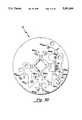
- FIG. 1is an isometric view of an antenna system according to the invention
- FIG. 1Ais cross sectional view, somewhat distorted, of an antenna system according to the invention
- FIG. 2is a plan view of an array of patch radiators and a common dual band center feed according to the invention
- FIG. 2Ais a plan view of two of the patch radiators showing the location of probe feeds according to the invention
- FIG. 3is a plan view of a portion of each layer of a monopulse array antenna with a corporate feed according to the invention
- FIGS. 3A-3Fare plan views showing the microstrip circuitry of each layer of the monopulse array antenna with the corporate feed according to the invention.
- FIG. 4is an isometric view, partially torn away of the common dual band center feed according to the invention.
- FIG. 5is a diagrammatical sketch of the feed to provide monopulse sum and difference signals for the array according to the invention.
- an antenna system 100is shown to include a dual reflector antenna 110 (here adapted for W-band) having a main reflector 112 with an aperture 114.
- the feed circuit 14is located at the apex of the main reflector 112 to minimize the blockage effects of an array antenna 10 mounted behind the main reflector 112.
- the main reflector 112includes a dual dichroic surface 112a which will reflect W-band signals but pass other signals as described further hereinafter.
- the reflector antenna 110further includes a subreflector 116 disposed in alignment with the feed circuit 14.
- the subreflector 116includes a dichroic surface 128 with a foam support 130, wherein the dichroic surface 128 will reflect W-band signals but pass other signals.
- the antenna system 100further includes the array antenna 10 (here adapted for X-band) disposed behind the main reflector 112 separated by a dielectric spacer 16 wherein the feed circuit 14 is also an antenna element of the array antenna 10. With such an arrangement, an antenna system is provided wherein the array antenna provides low first sidelobe characteristics in both sum and delta signal patterns and very low far out RMS sidelobe levels for two orthogonal polarizations in a shared aperture environment.
- the W-band antennais a dual polarized Cassegrain reflector antenna which is nearly invisible at X-band. The latter is required since the reflectors of the W-band antenna are disposed in front of the X-band antenna. Since both antennas provide dual polarization characteristics, a fully dichroic subreflector 116 and main reflector 112 are required. Furthermore, to maximize the W-band aperture, a flat main reflector 112 is used.
- the main reflector 112is here provided as a flat, circularly shaped dielectric sheet with a plurality of so-called cross dipole strip conductors 118 disposed on the dielectric surface 112a thereof and a dichroic layer of cross dipole strip conductors on a second surface (not shown) thereof.
- the various length cross dipole strip conductors 118are disposed to provide the main reflector 112 with electrical characteristics similar to a surface having a parabolic shape as shown in the teachings of U.S. Pat. No. 4,905,014 entitled "Microwave Phasing Structures For Electromagnetically Emulating Reflective Surfaces and Focusing Elements of Selected Geometry", issued to Gonzalez et al.
- the dichroic layer on the second surfaceserves to provide an effective ground plane to surface 112a, but is transparent to the array antenna 10.
- the main reflector 112may be provided as a single layer dichroic member having a parabolically shaped surface.
- the main reflector 112includes two parallel frequency selective surfaces separated by a thin (i.e. 0.010 inch thick) dielectric substrate which emulate a metallic parabolic surface at W-band while providing a low loss transmission path at X-band.
- the main reflector 112is separated from the X-band antenna 10 by a low dielectric constant foam spacer 16 (here approximately 0.100 inches thick) to minimize disturbance to the X-band patch radiator characteristics.
- the subreflector 116is provided with the dichroic surface 128 which will reflect W-band signals but pass other signals.
- the subreflector 116is supported by, here four, members 120, 122, 124 and 126, which are connected between the main reflector 112 and the subreflector 116, as shown, to secure the subreflector 116 in a fixed position relative to the main reflector 112.
- the thin support members 120 ... 126are here provided from a material having sufficient mechanical strength to support the subreflector 116. Those of skill in the art will also recognize that it is desirable to arrange support members 120 ... 126 to minimize the amount of blockage provided to electromagnetic signals which propagate from the main reflector 112 toward the subreflector 116.
- the support members 120 ... 126are provided with a rectangular cross sectional shape and having a so-called knife-edge.
- the knife-edge of the support members 120 ... 126are directed toward the direction of the propagating electric field.
- the support members 120 ... 126have a relatively small cross-sectional area and thus a relatively small blockage to propagating electromagnetic signals.
- other known techniques for affixing the position of the subreflector 116 relative to the feed circuit 14can be employed.
- a cylindrical member having a first base connected to the feed circuit 14 and a second base connected to the subreflector 116could be used.
- Such a cylindrical membermust have a low relative dielectric constant and provide low insertion loss and phase dispersion characteristics to radio frequency (RF) signals.
- RFradio frequency
- the antenna system 100may operate in either a transmit or a receive mode.
- the operation of the antenna system 100 and in particular the operation of the dual reflector antenna 110may be more easily understood by following the path of an electromagnetic signal while the reflector antenna 110 operates in a receive mode.
- RFradio frequency
- the main reflector 112reflects the RF signals captured toward the curved subreflector 116.
- the dichroic surface 112a with the plurality of so-called cross dipole strip conductors 118 of the main reflector 112is selected such that electromagnetic signals reflected therefrom propagate toward the subreflector 116.
- the RF signalreflects off the dichroic surface 128 of the subreflector 116 and propagates towards the feed circuit 14.
- the subreflector 116intercepts all of the RF signals or electromagnetic energy fed thereto from the main reflector 112.
- the feed circuit 14 and placement of the feed circuit 14 in the aperture 114are selected such that the RF signals emitted from the first port 14a of the feed circuit 14 when in the transmit mode is incident upon or "illuminates" the complete dichroic surface 128 of the subreflector 116 while minimizing the amount of RF energy which propagates beyond the edges of the dichroic surface 128 of the subreflector 116 (i.e. minimizing the so-called spillover energy).
- essentially all of the RF signals captured by the main reflector 112are reflected by the subreflector 116 and fed to the first port 14 a of the feed circuit 14.
- the RF signalspropagate along the feed circuit 14 to the second port 14b wherein such signals are coupled, via a quasioptical rotary joint (not shown), to a diplexer (not shown), such as a diplexer described in U.S. Pat. No. 5,034,750, entitled “Pulse Radar and Components Therefor", issued Jul. 23, 1991 and assigned to the same assignee as the present application, for further processing.
- a diplexernot shown
- the feed circuit 14is a cylindrical tube including a lens 18 to focus the signal from the diplexer (not shown) entering port 14b to a focal plane of appropriate size and located to correspond with the focal plane of the subreflector 116 and to also focus the RF signals from the subreflector 116 entering port 14a to a focal plane of appropriate size and located to correspond with the focal plane of a propagation circuit (not shown) wherein the RF signal is coupled to the diplexer (not shown).
- the array antenna 10includes, here, 44 dual polarized patch radiator elements 20 and one circular waveguide radiator element, the circular waveguide radiator element provided by the feed circuit 14.
- the 44 dual polarized patch radiator elements 20are grouped into eight segments 20a, 20b, 20c, 20d, 20e, 20f, 20g and 20h as shown.
- Segment 20aincludes patch radiator elements 20a 1 , 20a 2 , 20a 3 , 20a 4 , 20a 5 , 20a 6 , 20a v and 20a 8 disposed as shown.
- Segment 20bincludes eight patch radiator elements (not numbered) disposed as shown
- segment 20cincludes eight patch radiator elements (not numbered) disposed as shown
- segment 20dincludes eight patch radiator elements (not numbered) disposed as shown
- Segment 20eincludes patch radiator elements 20e 1 , 20e 2 and 20e 3 disposed as shown
- Segment 20fincludes three patch radiator elements (not numbered) disposed as shown
- segment 20gincludes three patch radiator elements (not numbered) disposed as shown
- segment 20hincludes three patch radiator elements (not numbered) disposed as shown.
- the eight segments 20a, 20b, 20c, 20d, 20e, 20f, 20g and 20h and the feed circuit 14provide a nine segment antenna configuration wherein all nine segments are used for the sum channel and 6 and 4 segments are used for the difference and Q channels, respectively, for monopulse processing as described further hereinafter.
- printed circuit techniquesare used to provide the RF segment distribution networks, monopulse circuitry and patch radiating elements.
- a corporate type feed network with equal path lengthsis utilized.
- the printed circuit board constructionresults in an X-band antenna that is less than 0.5 inches thick.
- the array antenna 10further includes several layers of printed circuits wherein the front layer includes the patch radiating elements 20 and each successive layer includes the required signal distribution and monopulse arithmetic circuitry required for dual polarization.
- the array antenna 10is here shown to include eight layers of printed circuit boards including a parasitic radiator board 22, a patch element board 24, a horizontal feed board 26, a vertical feed board 28, a phase matching board 30, a horizontal monopulse board 32, a vertical monopulse board 34 and a central element board 36.
- RF signalsare coupled from one of the printed circuit boards to another one of the printed circuit boards by interboard coaxial TEM mode RF feed through (not shown).
- a pin and socket arrangementis utilized as the center conductor of the coaxial section and is soldered to the stripline circuitry on each of the layers being connected.
- Intervening layers between circuits being connectedinclude appropriate coaxial sections formed by plated outer conductor holes and sized dielectric plug inserts.
- Four-port stripline hybridsare used throughout the signal distribution and monopulse combining circuitry.
- Wilkinson-type power dividersare used in the feed distribution networks and single-section branchline couplers are used in the monopulse combining networks.
- Mode suppression holesare installed in each stripline layer around each right angle transition as required and a conductive epoxy bond film is inserted between each board to provide a continuous ground between each one of the stripline boards.
- each of the antenna elements 20a 1 ... 20h 3include a stacked square microstrip patch radiator.
- the stacked square patch radiator antenna elementis fed by a pair of coaxial probes with a first probe located in a corner and a second probe located in an adjacent corner.
- the lower patchis fed by a probe from a corresponding feed board while the upper patch is electromagnetically coupled to increase the bandwidth and gain of the antenna element.
- a feed probe (not numbered) of each patch on the patch element board 24is coupled with stripline circuitry on the horizontal feed board 26 to provide a horizontally polarized signal.
- a feed probe (not numbered) of each patch on the patch element board 24is coupled with stripline circuitry on the vertical feed board 28 to provide a vertically polarized signal.
- the location of each feed probe (not numbered)is shown in FIG. 2.
- Cross polarization on-axis sensitivityis decreased by placing each probe on alternate patches as shown if FIG. 2 so that a 180 degrees phase reversal would normally occur, but by adding a corresponding additional 180 degrees of path length in the feed circuit for the respective elements, an in phase copolarized signal is provided.
- FIG. 3Ashows detailed microstrip circuitry of the horizontal feed board 26.
- the X-band array antenna 10(FIG. 1) operates in both a transmit and a receive mode, for explanation of operation we will assume we are in a receive mode.
- the horizontally polarized signal from each antenna element within each segmentare combined to provide eight output signals corresponding to the eight segments 20a ... 20h of FIG. 2.
- An impedance matching techniqueis used between each coaxial feed probe point and a corresponding stripline power divider on the horizontal feed board 26.
- a 50 ohm feed through with a 70 ohm section of transmission lineis used to couple a feed probe point to the horizontal feed board 26.
- Microstrip circuitry disposed as shown with Wilkinson-type power dividerscouples each of the feed through 30a 1 ... 30a 8 together to feed through 50a H .
- the lattercouples signals from each of the feed through 30a 1 ... 30a 8 together to provide a combined horizontally polarized signal at the feed through 50a H .
- each of the feed through coupled to a corresponding horizontal feed probe of the patches of segment 20bare coupled together to provide a combined horizontally polarized signal at feed through 50b H .
- Each of the feed throughs coupled to a corresponding horizontal feed probe of the patches of segment 20care coupled together to provide a combined horizontally polarized signal at feed through 50c H .
- Each of the feed through coupled to a corresponding horizontal feed probe of the patches of segment 20dare coupled together to provide a combined horizontally polarized signal at feed through 50d H .
- Each of the feed throughs coupled to a corresponding horizontal feed probe of the patches of segment 20eare coupled together to provide a combined horizontally polarized signal at feed through 50e H .
- Each of the feed throughs coupled to a corresponding horizontal feed probe of the patches of segment 20fare coupled together to provide a combined horizontally polarized signal at feed through 50f H .
- Each of the feed throughs coupled to a corresponding horizontal feed probe of the patches of segment 20gare coupled together to provide a combined horizontally polarized signal at feed through 50g H .
- each of the feed throughs coupled to a corresponding horizontal feed probe of the patches of segment 20hare coupled together to provide a combined horizontally polarized signal at feed through 50h H .
- FIG. 3Bshows detailed microstrip circuitry of the vertical feed board 28.
- the vertically polarized signal from each antenna element within each segmentare combined to provide eight output signals corresponding to the eight segments 20a ... 20h of FIG. 2.
- An impedance matching techniqueis used between each coaxial feed probe point and a corresponding stripline power divider on the vertical feed board 28.
- a 60 ohm feed through with a 75 ohm section of transmission lineis used to couple a feed probe point to the vertical feed board 28.
- feed through 40a 1is coupled to patch 20a 1
- feed through 40a 2is coupled to patch 20a 2
- feed through 40a 3is coupled to patch 20a 3
- feed through 40a 4is coupled to patch 20a 4
- feed through 40a 5is coupled to patch 20a 5
- feed through 40a 6is coupled to patch 20a 6
- feed through 40a 7is coupled to patch 20a 7
- feed through 40a 8is coupled to patch 20a 8 .
- Microstrip circuitry disposed as shown with Wilkinson-type power dividers(not numbered) couples each of the feed throughs 40a 1 ...
- each of the feed throughs coupled to a corresponding vertical feed probe of the patches of segment 20bare coupled together to provide a combined vertically polarized signal at feed through 50b v .
- Each of the feed throughs coupled to a corresponding vertical feed probe of the patches of segment 20care coupled together to provide a combined vertically polarized signal at feed through 50c v .
- Each of the feed throughs coupled to a corresponding vertical feed probe of the patches of segment 20dare coupled together to provide a combined vertically polarized signal at feed through 50d v .
- Each of the feed throughs coupled to a corresponding vertical feed probe of the patches of segment 20eare coupled together to provide a combined vertically polarized signal at feed through 50e v .
- Each of the feed throughs coupled to a corresponding vertical feed probe of the patches of segment 20fare coupled together to provide a combined vertically polarized signal at feed through 50f v .
- Each of the feed throughs coupled to a corresponding vertical feed probe of the patches of segment 20gare coupled together to provide a combined vertically polarized signal at feed through 50g v .
- each of the feed throughs coupled to a corresponding vertical feed probe of the patches of segment 20hare coupled together to provide a combined vertically polarized signal at feed through 50h v .
- FIG. 3Cshows detailed microstrip circuitry of the phase matching board 30.
- the positioning of various network inputs and outputsrequires the necessity to phase match the total transmission line length to each antenna element.
- Phase matching circuitry on the phase matching board 30provides the necessary phase match.
- Feed through 52a His coupled to feed through 50a H wherein the horizontally polarized signal from segment 20a is coupled to the phase matching board 30.
- Feed through 52a vis coupled to feed through 50a v wherein the vertically polarized signal from segment 20a is coupled to the phase matching board 30.
- Microstrip circuitryconnects the feed through 52a H to a feed through 54a H wherein a predetermined amount of phase difference is imparted to a signal propagating thereon to provide the necessary phase match.
- microstrip circuitry imparting the necessary phase shift to a signal propagating thereonconnects feed through 52a v to feed through 54a v .
- Feed through 52b His coupled to feed through 50b H wherein the horizontally polarized signal from segment 20b is coupled to the phase matching board 30.
- Feed through 52b vis coupled to feed through 50b v wherein the vertically polarized signal from segment 20b is coupled to the phase matching board 30.
- Microstrip circuitryconnects feed through 52b H to feed through 54b H and microstrip circuitry connects feed through 52b v to feed through 52b v . Furthermore, feed throughs 52c H , 52c v , 52d H , 52d v , 52e H , 52e v , 52f H , 52f v , 52g H , 52g v , 52h H and 52h v are coupled respectively to feed throughs 50c H , 50c v , 50d H , 50d v , 50e H , 50e v , 50f H , 50f v , 50g H , 50g v , 50h H and 50h v .
- Microstrip circuitryconnects feed throughs 52c H , 52c v , 52d H , 52d v , 52e H , 52e v , 52f H , 52f v , 52g H , 52g v , 52h H and 52h v , respectively to feed throughs 54c H , 54c v , 54d H , 54d v , 54e H , 54e v , 54f H , 54f v , 54 g H , 54g v , 54h H and 54h v as shown.
- Mode suppression holes(not numbered) are disposed around each right angle transitions as required.
- FIG. 3Dshows detailed microstrip circuitry of the horizontal monopulse board 32.
- the horizontal monopulse board 32includes a monopulse network to provide a sum signal, an azimuth difference signal, an elevation difference signal and a Q signal for the horizontally polarized signals.
- a feed through 56a His coupled to the feed through 54a H on the phase matching board 30.
- feed throughs 56b H , 56c H , 56d H , 56e H , 56f H , 56g H and 56h Hare respectively coupled to the feed throughs 54b H , 54b H , 54c H , 54d H , 54e H , 54f H , 54g H and 54h H on the phase matching board 30.
- microstrip circuitryis used to combine the horizontally polarized signals from the antenna segments 20a ... 20 h as required to implement the horizontal signal monopulse arithmetic network.
- the horizontal monopulse azimuth difference signalis provided.
- the horizontal monopulse elevation difference signalis provided.
- the horizontal monopulse Q signalis provided.
- the central element board 36combines the signals from the feed probes of the feed element 14 (FIG. 1A).
- the horizontal feed probes (not shown) of the feed elementare coupled, via coaxial cables (not shown), to respective feed throughs 62a, 62b.
- a Wilkinson-type power divider 66is used to couple the two signals from the feed throughs 62a, 62b to a feed through 60p H .
- the feed through 60p Hcouples the horizontally polarized signal from the horizontal feed probes (not shown) to the horizontal monopulse board 32.
- the vertical feed probes(not shown) are coupled, via coaxial cables (not shown), to respective feed throughs 64a, 64b.
- a Wilkinson-type power divider 68is used to couple the two signals from the feed throughs 64a, 64b to a feed through 60p v .
- the feed through 60p vcouples the vertically polarized signal from the vertical feed probes (not shown) to the vertical monopulse board 34 (FIG. 3E) .
- a feed through 58p Hwhich is coupled to the feed through 60p H (FIG. 3F), is connected to a single section edge line coupler 62.
- the single section edge line coupler 62is used to couple a portion of the sum signal which was combined from the feed throughs 56a H , 56b H , 56c H , 56d H , 56e H , 56f H , 56g H and 56h H with the portion of the sum signal from the feed through 58p H .
- the output port of the single section edge line coupler 62is coupled to a feed through 58 SH wherein the horizontally polarized monopulse sum signal is provided.
- FIG. 3Eshows detailed microstrip circuitry of the vertical monopulse board 34.
- the vertical monopulse board 34includes a monopulse network to provide a sum signal, an azimuth difference signal, an elevation difference signal and a Q signal for the vertically polarized signals.
- a feed through 56a vis coupled to the feed through 54a v on the phase matching board 30.
- feed throughs 56b v , 56c v , 56d v , 56e v , 56f v , 56g v and 56h vare respectively coupled to the feed throughs 54b v , 54b v , 54c v , 54d v , 54e v , 54f v , 54g v and 54h v on the phase matching board 30.
- microstrip circuitryis used to combine the vertically polarized signals from the antenna segments 20a ... 20h as required to implement the vertical signal monopulse arithmetic network.
- the vertical monopulse azimuth difference signalis provided.
- the vertical monopulse elevation difference signalis provided.
- the vertical monopulse Q signalis provided.
- a feed through 58p vwhich is connected to the feed through 60p v (FIG. 3F), is coupled to a single section edge line coupler 72.
- the single section edge line coupler 72is used to couple a portion of the sum signal which was combined from the feed throughs 56a.sub.
- the output port of the single section edge line coupleris coupled to a feed through 58 sv wherein the vertically polarized sum signal is provided.
- a terminating resistor(not numbered) is connected to the remaining port of the single section edge line coupler 72 to terminate the uncoupled port.
- four-port stripline hybridsare used throughout the signal distribution and monopulse combining circuitry.
- Wilkinson-type power dividersare used in the feed distribution networks.
- Single-section branchline couplersare used in the monopulse combining networks.
- Coaxial TEMRF feed throughsare utilized to couple energy between the various stripline circuit boards.
- Mode suppression holesare installed in each stripline layer around each right angle transition and a conductive epoxy bond film is inserted between each board to provide a continuous ground between each stripline layer.
- a pin and socket arrangementis utilized as the center conductor of each coaxial section and is soldered to the stripline circuitry on each of the layers being connected.
- Intervening layers between circuits being connectedinclude appropriate coaxial sections formed by plated outer conductor holes and sized dielectric plug inserts.
- the feed circuit 14 functioning as the center element of the array antenna 10is here an open ended circular waveguide.
- the feed circuit 14is excited by two probes (not numbered) for each polarization to provide a TE11 mode signal and suppress the TM01 mode signal at X-band.
- Signals from the two pairs of exciter probesare connected to the central element board 36, combined and added to the sum port of each polarization of the X-band signals.
- a plate 92 with a slotted dichroic surface 92sis disposed behind the exciter probes to block X-band signals from propagating in that direction but allowing W-band signals to pass freely.
- a lens 94here made of alumina, is shown behind the plate 92 to control the beam waist of the W-band signal.
- the lens 94is disposed at a location to focus the Gaussian beam of the W-band signal to form a virtual focal plane slightly beyond the main reflector 112 (FIG. 1). Knowing the characteristics of the Gaussian beam size, the X-band exciter probes are disposed to minimize interference with the W-band signal.
- Antenna segment 20a, 20b, 20c, 20d, 20e, 20f, 20g and 20hare shown to provide respective signals S 1 , S 2 , S 3 , S 4 , S 6 , S 8 and S 7 .
- Antenna segment 20ihere provided by feed circuit 14 (FIG. 1), provides signal S 9 .
- a plurality of power dividers 122a, 122b, 122c, 122d, 124a, 124b, 124c, 126a, 126b and 126care shown, each having a first and a second input port and a sum and a difference output port.
- a power divider 128 having a first and a second input port and an output portis also shown.
- the plurality of power dividers 122a ... 128are arranged as shown.
- the output signal S 1 of segment 20ais fed to the first input port of power divider 122c and the output signal S 2 of segment 20b is fed to the second input of power divider 122c wherein such signals are combined to provide a sum signal S 1 +S 2 at the sum output port and a difference signal S 1 -S 2 at the difference output port of power divider 122c.
- the output signal S 3 of segment 20cis fed to the first input port of power divider 122d and the output signal S 4 of segment 20d is fed to the second input of power divider 122d wherein such signals are combined to provide a sum signal S 3 +S 4 at the sum output port and a difference signal S 1 -S 4 at the difference output port of power divider 122d.
- the output signal S 5 of segment 20eis fed to the first input port of power divider 122a and the output signal S 6 of segment 20f is fed to the second input of power divider 122a wherein such signals are combined to provide a sum signal S 5 +S 6 at the sum output port and a difference signal S 5 -S 6 at the difference output port of power divider 122a.
- the output signal S 7 of segment 20his fed to the first input port of power divider 122b and the output signal S 8 of segment 20g is fed to the second input of power divider 122b wherein such signals are combined to provide a sum signal S 7 +S 8 at the sum output port and a difference signal S 7 -S 8 at the difference output port of power divider 122b.
- the sum signal S 1 +S 2is fed to the first input port of power divider 124b and the sum signal S 3 +S 4 is fed to the second input of power divider 124b wherein such signals are combined to provide a sum signal S 1 +S 2 +S 3 +S 4 at the sum output port and a difference signal S 1 +S 2 -S 3 -S 4 at the difference output port of power divider 124b.
- the sum signal S 5 +S 6is fed to the first input port of power divider 124a and the sum signal S 7 +S 8 is fed to the second input of power divider 124a wherein such signals are combined to provide a sum signal S 5 +S 6 +S 7 +S 8 at the sum output port and a difference signal S 5 +S 6 -S 7 -S 8 at the difference output port of power divider 124a.
- the difference signal S 5 +S 6 -S 7 -S 8is terminated with a terminating resistor 125 to ground.
- the difference signal S 1 -S 2is fed to the first input port of power divider 124c and the difference signal S 3 -S 4 is fed to the second input of power divider 124c wherein such signals are combined to provide a signal S 1 -S 2 +S 3 -S 4 at the sum output port and a signal S 1 -S 2 -S 3 +S 4 at the difference output port of power divider 124c.
- the signal S 1 -S 2 -S 3 +S 4 at the difference output port of power divider 124cis provided at an output port of the monopulse network 120 as the Q signal Q for the monopulse network 120.
- the sum signal S 5 +S 6 +S 7 +S 8is fed to the first input port of power divider 126a and the sum signal S 1 +S 2 +S 3 +S 4 is fed to the second input of power divider 126a wherein such signals are combined to provide a sum signal S 1 +S 2 +S 3 +S 4 +S 5 +S 6 +S 7 +S 8 at the sum output port and a signal at the difference output port of power divider 126a.
- the signal at the difference output port of power divider 126ais terminated with a terminating resistor 127a to ground.
- the sum signal S 1 +S 2 +S 3 +S 4 +S 5 +S 6 +S 7 +S 8is fed to power divider 128 wherein such signal is added to the signal S 9 and a composite sum signal ⁇ is provided at the output port of the power divider 128 which is the sum signal ⁇ for the monopulse network 120.
- the difference signal S 5 -S 6is fed to the first input port of power divider 126b and the difference signal S 1 +S 2 -S 3 -S 4 is fed to the second input of power divider 126b wherein such signals are combined to provide a signal (S 1 +S 2 +S 5 )-(S 3 +S 4 +S 6 ) at the sum output port and a signal at the difference output port of power divider 126b.
- the signal at the difference output port of power divider 126bis terminated with a terminating resistor 127b to ground.
- the signal (S 1 +S 2 +S 5 )-(S 3 +S 4 +S 6 ) at the sum output port of power divider 126bis provided at an output port of the monopulse network 120 as the elevation difference signal ⁇ e1 for the monopulse network 120.
- the difference signal S 7 -S 8is fed to the first input port of power divider 126c and the signal S 1 -S 2 'S 3 -S 4 is fed to the second input of power divider 126c wherein such signals are combined to provide a signal (S 1 +S 3 +S 7 )-(S 2 +S 4 +S 8 ) at the sum output port and a signal at the difference output port of power divider 126c.
- the signal at the difference output port of power divider 126cis terminated with a terminating resistor 127c to ground.
- the signal (S 1 +S 3 +S 7 )-(S 2 +S 4 +S 8 ) at the sum output port of power divider 126cis provided at an output port of the monopulse network 120 as the azimuth difference signal ⁇ az for the monopulse network 120.
- the above described monopulse network 120is implemented for the horizontally polarized signals provided from each of the segments 20a ... 20i and is also implemented for the vertically polarized signals provided from each of the segments 20a ... 20i.
Landscapes
- Physics & Mathematics (AREA)
- Electromagnetism (AREA)
- Variable-Direction Aerials And Aerial Arrays (AREA)
- Waveguide Aerials (AREA)
Abstract
Description
This invention relates to radar seekers used in guided missiles and more particularly to antenna systems for radar seekers operating at dual frequency bands.
As is known in the art, a reflector antenna generally includes a feed circuit and at least one conductive member generally referred to as a reflector. The feed circuit radiates RF energy at the reflector and the reflector directs the RF energy in a desired direction. Reflector antennas are used in those applications requiring an electrically large antenna having a high gain characteristic. In order to allow positioning of the feed element and electronics in a more convenient location, a dual reflector antenna system is sometimes used. One type of dual reflector antenna system is generally referred to as a Cassegrain reflector antenna.
A Cassegrain reflector antenna typically includes a first or main reflector having a parabolic shape with an aperture centrally disposed therein. A second, or subreflector having a hyperbolic shape is placed between the vertex of the main reflector and the prime focus of the main reflector. The precise location of the subreflector relative to the main reflector may be selected to provide an antenna having preselected electrical characteristics. A feed, generally referred to as a Cassegrain feed, is disposed in the aperture of the main reflector. In a transmit mode, the feed radiates electromagnetic energy at the subreflector. In a preferred situation, the subreflector intercepts substantially all of the electromagnetic energy and reflects such energy back toward the main reflector. The main reflector intercepts substantially all of the electromagnetic energy fed from the subreflector and reflects such electromagnetic energy in a desired direction. The geometrical arrangement of the parabolically shaped main reflector and the hyperbolically shaped subreflector are selected such that electromagnetic signals (or rays) reflected by the main reflector will be parallel.
As is also known, an array antenna includes a plurality of antenna elements disposed in an array in a manner wherein the radio frequency signals emanating from each of the plurality of antenna elements combine with constructive interference in a desired direction. In radar guided missiles, missile seeker antennas are often disposed on a gimbal. It is desirable in radar guided missiles to provide missile seeker antennas having polarimetric receive properties and which operate in dual frequency bands. In a radar guided missile application, a dual band dual polarized antenna must share a common radiating aperture to provide antenna radiation characteristics with high directivity and relatively low sidelobe levels at both bands. To operate in dual frequency bands, it is often necessary to provide two antenna assemblies and dispose such assemblies in the shared aperture. It is increasingly more difficult to dispose two antenna assemblies in a shared aperture in the small diameter of a missile.
With the foregoing background of this invention in mind, it is a primary object of this invention to provide a dual polarized dual band antenna with a common aperture.
Another object of this invention is to provide a dual band antenna with improved gain.
Still another object of this invention is to provide a dual band antenna with reduced sidelobe levels.
The foregoing and other objects of this invention are met generally by an antenna system including a reflector antenna, responsive to radio frequency signals at a first frequency, having a first reflector surface, a second reflector surface and a Cassegrain feed. The antenna system further includes an array antenna having a plurality of antenna elements responsive to radio frequency signals having a second different frequency, wherein a center element is in a common location with the feed of the reflector antenna. With such an arrangement, an improved dual band antenna system is provided. By providing the center element of the array antenna in a common location with the feed of the reflector antenna, a dual band radio frequency antenna system is provided which is more compact with improved radiation characteristics than known similar configured antennas.
For a more complete understanding of this invention, reference is now made to the following description of the accompanying drawings, wherein:
FIG. 1 is an isometric view of an antenna system according to the invention;
FIG. 1A is cross sectional view, somewhat distorted, of an antenna system according to the invention;
FIG. 2 is a plan view of an array of patch radiators and a common dual band center feed according to the invention;
FIG. 2A is a plan view of two of the patch radiators showing the location of probe feeds according to the invention;
FIG. 3 is a plan view of a portion of each layer of a monopulse array antenna with a corporate feed according to the invention;
FIGS. 3A-3F are plan views showing the microstrip circuitry of each layer of the monopulse array antenna with the corporate feed according to the invention;
FIG. 4 is an isometric view, partially torn away of the common dual band center feed according to the invention; and
FIG. 5 is a diagrammatical sketch of the feed to provide monopulse sum and difference signals for the array according to the invention.
Referring now to FIGS. 1 and 1A, anantenna system 100 is shown to include a dual reflector antenna 110 (here adapted for W-band) having amain reflector 112 with anaperture 114. Afeed circuit 14, having afirst port 14a and asecond port 14b, is disposed within theaperture 114. Thefeed circuit 14 is located at the apex of themain reflector 112 to minimize the blockage effects of anarray antenna 10 mounted behind themain reflector 112. Themain reflector 112 includes a dual dichroic surface 112a which will reflect W-band signals but pass other signals as described further hereinafter. Thereflector antenna 110 further includes asubreflector 116 disposed in alignment with thefeed circuit 14. Thesubreflector 116 includes adichroic surface 128 with afoam support 130, wherein thedichroic surface 128 will reflect W-band signals but pass other signals. Theantenna system 100 further includes the array antenna 10 (here adapted for X-band) disposed behind themain reflector 112 separated by adielectric spacer 16 wherein thefeed circuit 14 is also an antenna element of thearray antenna 10. With such an arrangement, an antenna system is provided wherein the array antenna provides low first sidelobe characteristics in both sum and delta signal patterns and very low far out RMS sidelobe levels for two orthogonal polarizations in a shared aperture environment.
The W-band antenna is a dual polarized Cassegrain reflector antenna which is nearly invisible at X-band. The latter is required since the reflectors of the W-band antenna are disposed in front of the X-band antenna. Since both antennas provide dual polarization characteristics, a fullydichroic subreflector 116 andmain reflector 112 are required. Furthermore, to maximize the W-band aperture, a flatmain reflector 112 is used.
Themain reflector 112 is here provided as a flat, circularly shaped dielectric sheet with a plurality of so-called crossdipole strip conductors 118 disposed on the dielectric surface 112a thereof and a dichroic layer of cross dipole strip conductors on a second surface (not shown) thereof. The various length crossdipole strip conductors 118 are disposed to provide themain reflector 112 with electrical characteristics similar to a surface having a parabolic shape as shown in the teachings of U.S. Pat. No. 4,905,014 entitled "Microwave Phasing Structures For Electromagnetically Emulating Reflective Surfaces and Focusing Elements of Selected Geometry", issued to Gonzalez et al. It is desirable to use such a reflector shape since, inter alia, such a flat surface allows more room for gimbal positioning and is cheaper and easier to manufacture than a parabolic surface. The dichroic layer on the second surface serves to provide an effective ground plane to surface 112a, but is transparent to thearray antenna 10. Alternatively, themain reflector 112 may be provided as a single layer dichroic member having a parabolically shaped surface.
Themain reflector 112 includes two parallel frequency selective surfaces separated by a thin (i.e. 0.010 inch thick) dielectric substrate which emulate a metallic parabolic surface at W-band while providing a low loss transmission path at X-band. Themain reflector 112 is separated from theX-band antenna 10 by a low dielectric constant foam spacer 16 (here approximately 0.100 inches thick) to minimize disturbance to the X-band patch radiator characteristics. Thesubreflector 116 is provided with thedichroic surface 128 which will reflect W-band signals but pass other signals. Thesubreflector 116 is supported by, here four,members main reflector 112 and thesubreflector 116, as shown, to secure thesubreflector 116 in a fixed position relative to themain reflector 112. Thethin support members 120 ... 126 are here provided from a material having sufficient mechanical strength to support thesubreflector 116. Those of skill in the art will also recognize that it is desirable to arrangesupport members 120 ... 126 to minimize the amount of blockage provided to electromagnetic signals which propagate from themain reflector 112 toward thesubreflector 116. Here, thesupport members 120 ... 126 are provided with a rectangular cross sectional shape and having a so-called knife-edge. The knife-edge of thesupport members 120 ... 126 are directed toward the direction of the propagating electric field. Thesupport members 120 ... 126 have a relatively small cross-sectional area and thus a relatively small blockage to propagating electromagnetic signals. Alternatively, other known techniques for affixing the position of thesubreflector 116 relative to thefeed circuit 14 can be employed. For example, a cylindrical member having a first base connected to thefeed circuit 14 and a second base connected to thesubreflector 116 could be used. Such a cylindrical member must have a low relative dielectric constant and provide low insertion loss and phase dispersion characteristics to radio frequency (RF) signals.
Theantenna system 100 may operate in either a transmit or a receive mode. The operation of theantenna system 100 and in particular the operation of thedual reflector antenna 110 may be more easily understood by following the path of an electromagnetic signal while thereflector antenna 110 operates in a receive mode. In the receive mode, radio frequency (RF) signals reflected from a potential target (not shown) propagates toward themain reflector 112. Themain reflector 112 reflects the RF signals captured toward thecurved subreflector 116. The dichroic surface 112a with the plurality of so-called crossdipole strip conductors 118 of themain reflector 112 is selected such that electromagnetic signals reflected therefrom propagate toward thesubreflector 116. The RF signal reflects off thedichroic surface 128 of thesubreflector 116 and propagates towards thefeed circuit 14. In a preferred situation, thesubreflector 116 intercepts all of the RF signals or electromagnetic energy fed thereto from themain reflector 112. Those of skill in the art will recognize that thefeed circuit 14 and placement of thefeed circuit 14 in theaperture 114 are selected such that the RF signals emitted from thefirst port 14a of thefeed circuit 14 when in the transmit mode is incident upon or "illuminates" the completedichroic surface 128 of thesubreflector 116 while minimizing the amount of RF energy which propagates beyond the edges of thedichroic surface 128 of the subreflector 116 (i.e. minimizing the so-called spillover energy). Alternatively, when in the receive mode, essentially all of the RF signals captured by themain reflector 112 are reflected by thesubreflector 116 and fed to thefirst port 14 a of thefeed circuit 14.
The RF signals propagate along thefeed circuit 14 to thesecond port 14b wherein such signals are coupled, via a quasioptical rotary joint (not shown), to a diplexer (not shown), such as a diplexer described in U.S. Pat. No. 5,034,750, entitled "Pulse Radar and Components Therefor", issued Jul. 23, 1991 and assigned to the same assignee as the present application, for further processing. The details offeed circuit 14 will be described further hereinafter. Suffice it to say now, thefeed circuit 14 is a cylindrical tube including alens 18 to focus the signal from the diplexer (not shown) enteringport 14b to a focal plane of appropriate size and located to correspond with the focal plane of thesubreflector 116 and to also focus the RF signals from thesubreflector 116 enteringport 14a to a focal plane of appropriate size and located to correspond with the focal plane of a propagation circuit (not shown) wherein the RF signal is coupled to the diplexer (not shown).
Referring now also to FIG. 2, thearray antenna 10 includes, here, 44 dual polarizedpatch radiator elements 20 and one circular waveguide radiator element, the circular waveguide radiator element provided by thefeed circuit 14. The 44 dual polarizedpatch radiator elements 20 are grouped into eightsegments Segment 20b includes eight patch radiator elements (not numbered) disposed as shown,segment 20c includes eight patch radiator elements (not numbered) disposed as shown andsegment 20d includes eight patch radiator elements (not numbered) disposed as shown.Segment 20e includespatch radiator elements segment 20g includes three patch radiator elements (not numbered) disposed as shown andsegment 20h includes three patch radiator elements (not numbered) disposed as shown. The eightsegments feed circuit 14 provide a nine segment antenna configuration wherein all nine segments are used for the sum channel and 6 and 4 segments are used for the difference and Q channels, respectively, for monopulse processing as described further hereinafter. To provide a low profile, printed circuit techniques are used to provide the RF segment distribution networks, monopulse circuitry and patch radiating elements. To provide the requisite frequency bandwidth, a corporate type feed network with equal path lengths is utilized. The printed circuit board construction results in an X-band antenna that is less than 0.5 inches thick. Thearray antenna 10 further includes several layers of printed circuits wherein the front layer includes thepatch radiating elements 20 and each successive layer includes the required signal distribution and monopulse arithmetic circuitry required for dual polarization.
Referring now to FIG. 3, thearray antenna 10 is here shown to include eight layers of printed circuit boards including aparasitic radiator board 22, apatch element board 24, ahorizontal feed board 26, avertical feed board 28, aphase matching board 30, ahorizontal monopulse board 32, avertical monopulse board 34 and acentral element board 36. RF signals are coupled from one of the printed circuit boards to another one of the printed circuit boards by interboard coaxial TEM mode RF feed through (not shown). A pin and socket arrangement is utilized as the center conductor of the coaxial section and is soldered to the stripline circuitry on each of the layers being connected. Intervening layers between circuits being connected include appropriate coaxial sections formed by plated outer conductor holes and sized dielectric plug inserts. Four-port stripline hybrids are used throughout the signal distribution and monopulse combining circuitry. Wilkinson-type power dividers are used in the feed distribution networks and single-section branchline couplers are used in the monopulse combining networks. Mode suppression holes are installed in each stripline layer around each right angle transition as required and a conductive epoxy bond film is inserted between each board to provide a continuous ground between each one of the stripline boards.
Referring now to FIGS. 2, 2A and 3, each of the antenna elements 20a1 ... 20h3 include a stacked square microstrip patch radiator. To provide low cross-polarization, good VSWR match and high radiation efficiency over a desired frequency bandwidth, the stacked square patch radiator antenna element is fed by a pair of coaxial probes with a first probe located in a corner and a second probe located in an adjacent corner. The lower patch is fed by a probe from a corresponding feed board while the upper patch is electromagnetically coupled to increase the bandwidth and gain of the antenna element. Thus, a feed probe (not numbered) of each patch on thepatch element board 24 is coupled with stripline circuitry on thehorizontal feed board 26 to provide a horizontally polarized signal. Furthermore, a feed probe (not numbered) of each patch on thepatch element board 24 is coupled with stripline circuitry on thevertical feed board 28 to provide a vertically polarized signal. The location of each feed probe (not numbered) is shown in FIG. 2. Cross polarization on-axis sensitivity is decreased by placing each probe on alternate patches as shown if FIG. 2 so that a 180 degrees phase reversal would normally occur, but by adding a corresponding additional 180 degrees of path length in the feed circuit for the respective elements, an in phase copolarized signal is provided. The sense of polarization for the cross polarized component is unaffected by the reversal in probe location, however, a 180 degrees phase reversal due to the added length in the feed circuit occurs, such that alternate patches have a 180 degrees phase difference in cross polarized energy thereby decreasing the on-axis cross polarization sensitivity.
Referring now to FIGS. 2 and 3A, FIG. 3A shows detailed microstrip circuitry of thehorizontal feed board 26. Although the X-band array antenna 10 (FIG. 1) operates in both a transmit and a receive mode, for explanation of operation we will assume we are in a receive mode. Here, the horizontally polarized signal from each antenna element within each segment are combined to provide eight output signals corresponding to the eight segments 20a ... 20h of FIG. 2. An impedance matching technique is used between each coaxial feed probe point and a corresponding stripline power divider on thehorizontal feed board 26. A 50 ohm feed through with a 70 ohm section of transmission line is used to couple a feed probe point to thehorizontal feed board 26. Microstrip circuitry disposed as shown with Wilkinson-type power dividers (not numbered) couples each of the feed through 30a1 ... 30a8 together to feed through 50aH. The latter couples signals from each of the feed through 30a1 ... 30a8 together to provide a combined horizontally polarized signal at the feed through 50aH. In a similar manner, each of the feed through coupled to a corresponding horizontal feed probe of the patches ofsegment 20b are coupled together to provide a combined horizontally polarized signal at feed through 50bH. Each of the feed throughs coupled to a corresponding horizontal feed probe of the patches ofsegment 20c are coupled together to provide a combined horizontally polarized signal at feed through 50cH. Each of the feed through coupled to a corresponding horizontal feed probe of the patches ofsegment 20d are coupled together to provide a combined horizontally polarized signal at feed through 50dH. Each of the feed throughs coupled to a corresponding horizontal feed probe of the patches ofsegment 20e are coupled together to provide a combined horizontally polarized signal at feed through 50eH. Each of the feed throughs coupled to a corresponding horizontal feed probe of the patches of segment 20f are coupled together to provide a combined horizontally polarized signal at feed through 50fH. Each of the feed throughs coupled to a corresponding horizontal feed probe of the patches ofsegment 20g are coupled together to provide a combined horizontally polarized signal at feed through 50gH. Finally, each of the feed throughs coupled to a corresponding horizontal feed probe of the patches ofsegment 20h are coupled together to provide a combined horizontally polarized signal at feed through 50hH.
Referring now to FIGS. 2 and 3B, FIG. 3B shows detailed microstrip circuitry of thevertical feed board 28. Here, the vertically polarized signal from each antenna element within each segment are combined to provide eight output signals corresponding to the eight segments 20a ... 20h of FIG. 2. An impedance matching technique is used between each coaxial feed probe point and a corresponding stripline power divider on thevertical feed board 28. A 60 ohm feed through with a 75 ohm section of transmission line is used to couple a feed probe point to thevertical feed board 28. Insegment 40a of thevertical feed board 28, which corresponds to segment 20a of FIG.2, feed through 40a1 is coupled to patch 20a1, feed through 40a2 is coupled to patch 20a2, feed through 40a3 is coupled to patch 20a3, feed through 40a4 is coupled to patch 20a4, feed through 40a5 is coupled to patch 20a5, feed through 40a6 is coupled to patch 20a6, feed through 40a7 is coupled to patch 20a7 and feed through 40a8 is coupled to patch 20a8. Microstrip circuitry disposed as shown with Wilkinson-type power dividers (not numbered) couples each of thefeed throughs 40a1 ... 40a8 coupled to a corresponding vertical feed probe of the patches of segment 20a together to provide a combined vertically polarized signal at the feed through 50av. In a similar manner, each of the feed throughs coupled to a corresponding vertical feed probe of the patches ofsegment 20b are coupled together to provide a combined vertically polarized signal at feed through 50bv. Each of the feed throughs coupled to a corresponding vertical feed probe of the patches ofsegment 20c are coupled together to provide a combined vertically polarized signal at feed through 50cv. Each of the feed throughs coupled to a corresponding vertical feed probe of the patches ofsegment 20d are coupled together to provide a combined vertically polarized signal at feed through 50dv. Each of the feed throughs coupled to a corresponding vertical feed probe of the patches ofsegment 20e are coupled together to provide a combined vertically polarized signal at feed through 50ev. Each of the feed throughs coupled to a corresponding vertical feed probe of the patches of segment 20f are coupled together to provide a combined vertically polarized signal at feed through 50fv. Each of the feed throughs coupled to a corresponding vertical feed probe of the patches ofsegment 20g are coupled together to provide a combined vertically polarized signal at feed through 50gv. Finally, each of the feed throughs coupled to a corresponding vertical feed probe of the patches ofsegment 20h are coupled together to provide a combined vertically polarized signal at feed through 50hv.
Referring now to FIGS. 3A, 3B, 3C, 3D, 3E and 3F, FIG. 3C shows detailed microstrip circuitry of thephase matching board 30. The positioning of various network inputs and outputs requires the necessity to phase match the total transmission line length to each antenna element. Phase matching circuitry on thephase matching board 30 provides the necessary phase match. Feed through 52aH is coupled to feed through 50aH wherein the horizontally polarized signal from segment 20a is coupled to thephase matching board 30. Feed through 52av is coupled to feed through 50av wherein the vertically polarized signal from segment 20a is coupled to thephase matching board 30. Microstrip circuitry connects the feed through 52aH to a feed through 54aH wherein a predetermined amount of phase difference is imparted to a signal propagating thereon to provide the necessary phase match. In a similar manner, microstrip circuitry imparting the necessary phase shift to a signal propagating thereon connects feed through 52av to feed through 54av. Feed through 52bH is coupled to feed through 50bH wherein the horizontally polarized signal fromsegment 20b is coupled to thephase matching board 30. Feed through 52bv is coupled to feed through 50bv wherein the vertically polarized signal fromsegment 20b is coupled to thephase matching board 30. Microstrip circuitry connects feed through 52bH to feed through 54bH and microstrip circuitry connects feed through 52bv to feed through 52bv. Furthermore, feed throughs 52cH, 52cv, 52dH, 52dv, 52eH, 52ev, 52fH, 52fv, 52gH, 52gv, 52hH and 52hv are coupled respectively to feed throughs 50cH, 50cv, 50dH, 50dv, 50eH, 50ev, 50fH, 50fv, 50gH, 50gv, 50hH and 50hv. Microstrip circuitry connects feed throughs 52cH, 52cv, 52dH, 52dv, 52eH, 52ev, 52fH, 52fv, 52gH, 52gv, 52hH and 52hv, respectively to feed throughs 54cH, 54cv, 54dH, 54dv, 54eH, 54ev, 54fH, 54fv, 54 gH, 54gv, 54hH and 54hv as shown. Mode suppression holes (not numbered) are disposed around each right angle transitions as required.
FIG. 3D shows detailed microstrip circuitry of thehorizontal monopulse board 32. Here, the horizontally polarized signals from each antenna segment are combined in a manner as to be described further in connection with FIG. 5. Thehorizontal monopulse board 32 includes a monopulse network to provide a sum signal, an azimuth difference signal, an elevation difference signal and a Q signal for the horizontally polarized signals. A feed through 56aH is coupled to the feed through 54aH on thephase matching board 30. Similarly, feed throughs 56bH, 56cH, 56dH, 56eH, 56fH, 56gH and 56hH are respectively coupled to the feed throughs 54bH, 54bH, 54cH, 54dH, 54eH, 54fH, 54gH and 54hH on thephase matching board 30. Using 4-port stripline hybrids (not numbered), here branch line hybrids, microstrip circuitry is used to combine the horizontally polarized signals from the antenna segments 20a ... 20 h as required to implement the horizontal signal monopulse arithmetic network. At feed through 58.sub.ΔZAH, the horizontal monopulse azimuth difference signal is provided. At feed through 58.sub.ΔELH, the horizontal monopulse elevation difference signal is provided. At feed through 58QH, the horizontal monopulse Q signal is provided.
Referring momentarily also to FIG. 3F, the detailed microstrip circuitry of thecentral element board 36 is shown. Thecentral element board 36 combines the signals from the feed probes of the feed element 14 (FIG. 1A). The horizontal feed probes (not shown) of the feed element are coupled, via coaxial cables (not shown), torespective feed throughs type power divider 66 is used to couple the two signals from thefeed throughs horizontal monopulse board 32. In a similar manner, the vertical feed probes (not shown) are coupled, via coaxial cables (not shown), torespective feed throughs type power divider 68 is used to couple the two signals from thefeed throughs
Referring now again to FIG. 3D, a feed through 58pH, which is coupled to the feed through 60pH (FIG. 3F), is connected to a single sectionedge line coupler 62. The single sectionedge line coupler 62 is used to couple a portion of the sum signal which was combined from the feed throughs 56aH, 56bH, 56cH, 56dH, 56eH, 56fH, 56gH and 56hH with the portion of the sum signal from the feed through 58pH. The output port of the single sectionedge line coupler 62 is coupled to a feed through 58SH wherein the horizontally polarized monopulse sum signal is provided. A terminating resistor (not numbered) is connected to the remaining port of the single sectionedge line coupler 62 to terminate the uncoupled port. Terminating resistors (not numbered) are also used, when required, to terminate an unused port of the 4-port stripline hybrids.
FIG. 3E shows detailed microstrip circuitry of thevertical monopulse board 34. Here, the vertically polarized signals from each antenna segment are combined in the manner as to be described further in connection with FIG. 5. Thevertical monopulse board 34 includes a monopulse network to provide a sum signal, an azimuth difference signal, an elevation difference signal and a Q signal for the vertically polarized signals. A feed through 56av is coupled to the feed through 54av on thephase matching board 30. Similarly, feed throughs 56bv, 56cv, 56dv, 56ev, 56fv, 56gv and 56hv are respectively coupled to the feed throughs 54bv, 54bv, 54cv, 54dv, 54ev, 54fv, 54gv and 54hv on thephase matching board 30. Using 4-port stripline hybrids (not numbered), here branch line hybrids, microstrip circuitry is used to combine the vertically polarized signals from the antenna segments 20a ... 20h as required to implement the vertical signal monopulse arithmetic network. At feed through 58.sub.ΔAZv, the vertical monopulse azimuth difference signal is provided. At feed through 58.sub.ΔELv, the vertical monopulse elevation difference signal is provided. At feed through 58Qv, the vertical monopulse Q signal is provided. A feed through 58pv, which is connected to the feed through 60pv (FIG. 3F), is coupled to a single sectionedge line coupler 72. The single sectionedge line coupler 72 is used to couple a portion of the sum signal which was combined from the feed throughs 56a.sub. v, 56bv, 56cv, 56dv, 56ev, 56fv, 56gv and 56hv with the portion of the sum signal from the feed through 58pv. The output port of the single section edge line coupler is coupled to a feed through 58sv wherein the vertically polarized sum signal is provided. A terminating resistor (not numbered) is connected to the remaining port of the single sectionedge line coupler 72 to terminate the uncoupled port.
As described hereinbefore, four-port stripline hybrids are used throughout the signal distribution and monopulse combining circuitry. Wilkinson-type power dividers are used in the feed distribution networks. Single-section branchline couplers are used in the monopulse combining networks. Coaxial TEMRF feed throughs are utilized to couple energy between the various stripline circuit boards. Mode suppression holes are installed in each stripline layer around each right angle transition and a conductive epoxy bond film is inserted between each board to provide a continuous ground between each stripline layer. A pin and socket arrangement is utilized as the center conductor of each coaxial section and is soldered to the stripline circuitry on each of the layers being connected. Intervening layers between circuits being connected include appropriate coaxial sections formed by plated outer conductor holes and sized dielectric plug inserts.
Referring now to FIG. 4, thefeed circuit 14 functioning as the center element of thearray antenna 10 is here an open ended circular waveguide. Thefeed circuit 14 is excited by two probes (not numbered) for each polarization to provide a TE11 mode signal and suppress the TM01 mode signal at X-band. Signals from the two pairs of exciter probes are connected to thecentral element board 36, combined and added to the sum port of each polarization of the X-band signals. Aplate 92 with a slotted dichroic surface 92s is disposed behind the exciter probes to block X-band signals from propagating in that direction but allowing W-band signals to pass freely. Alens 94, here made of alumina, is shown behind theplate 92 to control the beam waist of the W-band signal. Thelens 94 is disposed at a location to focus the Gaussian beam of the W-band signal to form a virtual focal plane slightly beyond the main reflector 112 (FIG. 1). Knowing the characteristics of the Gaussian beam size, the X-band exciter probes are disposed to minimize interference with the W-band signal.
Referring now to FIG. 5, a block diagram of a ninesegment monopulse network 120 here implemented is described.Antenna segments power dividers power divider 128 having a first and a second input port and an output port is also shown. To provide the requiredmonopulse network 120 with outputs including a sum signal, an azimuth difference signal, an elevation difference signal and a Q signal, the plurality of power dividers 122a ... 128 are arranged as shown. The output signal S1 of segment 20a is fed to the first input port of power divider 122c and the output signal S2 ofsegment 20b is fed to the second input of power divider 122c wherein such signals are combined to provide a sum signal S1 +S2 at the sum output port and a difference signal S1 -S2 at the difference output port of power divider 122c. The output signal S3 ofsegment 20c is fed to the first input port ofpower divider 122d and the output signal S4 ofsegment 20d is fed to the second input ofpower divider 122d wherein such signals are combined to provide a sum signal S3 +S4 at the sum output port and a difference signal S1 -S4 at the difference output port ofpower divider 122d. In a similar manner, the output signal S5 ofsegment 20e is fed to the first input port of power divider 122a and the output signal S6 of segment 20f is fed to the second input of power divider 122a wherein such signals are combined to provide a sum signal S5 +S6 at the sum output port and a difference signal S5 -S6 at the difference output port of power divider 122a. The output signal S7 ofsegment 20h is fed to the first input port ofpower divider 122b and the output signal S8 ofsegment 20g is fed to the second input ofpower divider 122b wherein such signals are combined to provide a sum signal S7 +S8 at the sum output port and a difference signal S7 -S8 at the difference output port ofpower divider 122b.
The sum signal S1 +S2 is fed to the first input port ofpower divider 124b and the sum signal S3 +S4 is fed to the second input ofpower divider 124b wherein such signals are combined to provide a sum signal S1 +S2 +S3 +S4 at the sum output port and a difference signal S1 +S2 -S3 -S4 at the difference output port ofpower divider 124b. Like wise, the sum signal S5 +S6 is fed to the first input port ofpower divider 124a and the sum signal S7 +S8 is fed to the second input ofpower divider 124a wherein such signals are combined to provide a sum signal S5 +S6 +S7 +S8 at the sum output port and a difference signal S5 +S6 -S7 -S8 at the difference output port ofpower divider 124a. Here, the difference signal S5 +S6 -S7 -S8 is terminated with a terminatingresistor 125 to ground. The difference signal S1 -S2 is fed to the first input port ofpower divider 124c and the difference signal S3 -S4 is fed to the second input ofpower divider 124c wherein such signals are combined to provide a signal S1 -S2 +S3 -S4 at the sum output port and a signal S1 -S2 -S3 +S4 at the difference output port ofpower divider 124c. The signal S1 -S2 -S3 +S4 at the difference output port ofpower divider 124c is provided at an output port of themonopulse network 120 as the Q signal Q for themonopulse network 120.
The sum signal S5 +S6 +S7 +S8 is fed to the first input port ofpower divider 126a and the sum signal S1 +S2 +S3 +S4 is fed to the second input ofpower divider 126a wherein such signals are combined to provide a sum signal S1 +S2 +S3 +S4 +S5 +S6 +S7 +S8 at the sum output port and a signal at the difference output port ofpower divider 126a. The signal at the difference output port ofpower divider 126a is terminated with a terminating resistor 127a to ground. The sum signal S1 +S2 +S3 +S4 +S5 +S6 +S7 +S8 is fed topower divider 128 wherein such signal is added to the signal S9 and a composite sum signal Σ is provided at the output port of thepower divider 128 which is the sum signal Σ for themonopulse network 120.
The difference signal S5 -S6 is fed to the first input port ofpower divider 126b and the difference signal S1 +S2 -S3 -S4 is fed to the second input ofpower divider 126b wherein such signals are combined to provide a signal (S1 +S2 +S5)-(S3 +S4 +S6) at the sum output port and a signal at the difference output port ofpower divider 126b. The signal at the difference output port ofpower divider 126b is terminated with a terminatingresistor 127b to ground. The signal (S1 +S2 +S5)-(S3 +S4 +S6) at the sum output port ofpower divider 126b is provided at an output port of themonopulse network 120 as the elevation difference signal Δe1 for themonopulse network 120.
The difference signal S7 -S8 is fed to the first input port ofpower divider 126c and the signal S1 -S2 'S3 -S4 is fed to the second input ofpower divider 126c wherein such signals are combined to provide a signal (S1 +S3 +S7)-(S2 +S4 +S8) at the sum output port and a signal at the difference output port ofpower divider 126c. The signal at the difference output port ofpower divider 126c is terminated with a terminatingresistor 127c to ground. The signal (S1 +S3 +S7)-(S2 +S4 +S8) at the sum output port ofpower divider 126c is provided at an output port of themonopulse network 120 as the azimuth difference signal Δaz for themonopulse network 120.
It should be appreciated the above describedmonopulse network 120 is implemented for the horizontally polarized signals provided from each of the segments 20a ... 20i and is also implemented for the vertically polarized signals provided from each of the segments 20a ... 20i.
Having described this invention, it will now be apparent to one of skill in the art that changes may be made without departing from the concept of providing a dual band, shared aperture antenna system including a reflector antenna, responsive to radio frequency signals at a first frequency, having a first reflector surface, a second reflector surface and a Cassegrain feed, the antenna system further including an array antenna having a plurality of antenna elements responsive to radio frequency signals having a second different frequency. It is felt, therefore, that this invention should not be restricted to its disclosed embodiment, but rather should be limited only by the spirit and scope of the appended claims.
Claims (16)
1. An antenna comprising:
(a) a reflector antenna having an aperture and responsive to radio frequency signals having a first frequency, the reflector antenna comprising:
a first reflector;
a second reflector; and
a Cassegrainian feed, the first reflector, the second reflector and the Cassegrainian feed disposed in a Cassegrain reflector antenna arrangement; and
(b) an array antenna having an aperture, the array antenna comprising a plurality of antenna elements, each one of the antenna elements responsive to radio frequency signals having a second different frequency, the array antenna and the reflector antenna having a common aperture, the Cassegrainian feed comprising means for propagating radio frequency signals having the second different frequency for providing one of the plurality of antenna elements of the array antenna; and
(c) a dielectric spacer disposed between the reflector antenna and the array antenna.
2. The antenna as recited in claim 1 wherein at least one of the plurality of antenna elements of the array antenna comprises:
(a) a dielectric layer having a first and second surface;
(b) a microstrip patch radiator element disposed adjacent the first surface of the dielectric layer; and
(c) a parasitic radiator element disposed adjacent the second surface of the dielectric layer.
3. The antenna as recited in claim 2 wherein the microstrip patch radiator element comprises a first feed probe to provide a horizontally polarized signal and a second feed probe to provide a vertically polarized signal.
4. The antenna as recited in claim 3 wherein the feed probe of alternating microstrip patch radiator elements are placed in opposing locations within the microstrip patch radiator element.
5. The antenna as recited in claim 4 wherein the plurality of antenna elements of the array antenna are disposed to provide a monopulse antenna element arrangement.
6. The antenna as recited in claim 5 further comprising microstrip circuitry disposed on a plurality of successively layered printed circuit boards, the microstrip circuitry disposed to perform monopulse arithmetic to provide a monopulse sum signal, a monopulse azimuth difference signal and a monopulse elevation difference signal in response to a received signal coupled to the microstrip circuitry from the plurality of antenna elements.
7. (Amended) An antenna comprising:
(a) a first substrate having a first and a second surface with an opening disposed from said first surface to said second surface, the first substrate further having a plurality of antenna elements, responsive to a signal having a first frequency, disposed adjacent the first surface and a corresponding plurality of parasitic antenna elements disposed adjacent the second surface;
(b) a second substrate having a first and a second surface with an opening disposed from said first surface to said second surface, the second substrate further having a metallic pattern disposed on the first surface of the second substrate, the metallic pattern providing a dichroic surface transparent to signals having the first frequency;
(c) a dielectric spacer disposed between said first substrate and said second substrate, and
(d) a Cassegrainian feed disposed in the opening of the first substrate and the opening of the second substrate, the Cassegrainian feed comprising means for feeding and receiving signals having the first frequency and for feeding and receiving signals having a second different frequency.
8. The antenna as recited in claim 7 wherein the plurality of antenna elements are disposed to provide a monopulse antenna element arrangement.
9. The antenna as recited in claim 8 further comprising microstrip circuitry disposed on a plurality of successively layered printed circuit boards, the microstrip circuitry disposed to perform monopulse arithmetic to provide a monopulse sum signal, a monopulse azimuth difference signal and a monopulse elevation difference signal in response to a received signal coupled to the microstrip circuitry from the plurality of antenna elements.
10. The antenna as recited in claim 9 wherein the microstrip circuitry disposed on a plurality of successively layered printed circuit boards comprises:
(a) a first printed circuit board having a plurality of inputs comprising microstrip circuity, connected to the plurality of inputs, disposed to perform monopulse arithmetic to provide a monopulse sum signal, a monopulse azimuth difference signal and a monopulse elevation difference signal;
(b) a second printed circuit board comprising microstrip circuitry to connect the plurality of antenna elements together into a plurality of outputs; and
(c) a third printed circuit board, disposed between the first printed circuit board and the second printed circuit board, the third printed circuit board comprising microstrip circuitry to provide requisite path lengths to connect the plurality of outputs of the second printed circuit board with the plurality of inputs of the first printed circuit board.
11. The antenna as recited in claim 9 further comprising a reflector antenna comprising:
(a) a first reflector; and
(b) a second reflector the first reflector, the second reflector and the Cassegrainian feed disposed in a Cassegrain reflector antenna arrangement.
12. An antenna comprising:
(a) first reflecting means for reflecting electromagnetic signals fed thereto, said first reflecting means having an opening therethrough;
(b) second reflecting means for reflecting electromagnetic signals fed thereto, said second reflecting means adapted to cooperate with said first reflecting means as a dual reflector antenna system;
(c) feed circuit means, disposed in the opening of said first reflecting means, for feeding and receiving electromagnetic signals having a first frequency to and from the second reflecting means and for feeding and receiving electromagnetic signals having a second different frequency; and
(d) emanating means, disposed adjacent the first reflecting means, for feeding and receiving electromagnetic signals having the second different frequency, wherein the emanating means comprises a plurality of antenna elements comprising:
a dielectric layer having a first and second surface;
a microstrip patch radiator element disposed adjacent the first surface of the dielectric layer; and
a parasitic radiator element disposed adjacent the second surface of the dielectric layer.
13. The antenna as recited in claim 12 wherein the microstrip patch radiator element comprises a first feed probe to provide a horizontally polarized signal and a second feed probe to provide a vertically polarized signal.
14. The antenna as recited in claim 13 wherein the feed probe of alternating microstrip patch radiator elements are placed in opposing locations within the microstrip patch radiator element.
15. The antenna as recited in claim 14 wherein the plurality of antenna elements are disposed to provide a monopulse antenna element arrangement.
16. The antenna as recited in claim 12 further comprising microstrip circuitry disposed on a plurality of successively layered printed circuit boards, the microstrip circuitry disposed to perform monopulse arithmetic to provide a monopulse sum signal, a monopulse azimuth difference signal and a monopulse elevation difference signal in response to a received signal coupled to the microstrip circuitry from the emanating means.
Priority Applications (1)
| Application Number | Priority Date | Filing Date | Title |
|---|---|---|---|
| US08/034,020US5451969A (en) | 1993-03-22 | 1993-03-22 | Dual polarized dual band antenna |
Applications Claiming Priority (1)
| Application Number | Priority Date | Filing Date | Title |
|---|---|---|---|
| US08/034,020US5451969A (en) | 1993-03-22 | 1993-03-22 | Dual polarized dual band antenna |
Publications (1)
| Publication Number | Publication Date |
|---|---|
| US5451969Atrue US5451969A (en) | 1995-09-19 |
Family
ID=21873816
Family Applications (1)
| Application Number | Title | Priority Date | Filing Date |
|---|---|---|---|
| US08/034,020Expired - LifetimeUS5451969A (en) | 1993-03-22 | 1993-03-22 | Dual polarized dual band antenna |
Country Status (1)
| Country | Link |
|---|---|
| US (1) | US5451969A (en) |
Cited By (204)
| Publication number | Priority date | Publication date | Assignee | Title |
|---|---|---|---|---|
| US5686929A (en)* | 1994-10-25 | 1997-11-11 | Siemens Aktiengesellschaft | RF homing head antenna system for missiles |
| US5831581A (en)* | 1996-08-23 | 1998-11-03 | Lockheed Martin Vought Systems Corporation | Dual frequency band planar array antenna |
| US6034649A (en)* | 1998-10-14 | 2000-03-07 | Andrew Corporation | Dual polarized based station antenna |
| US6072439A (en)* | 1998-01-15 | 2000-06-06 | Andrew Corporation | Base station antenna for dual polarization |
| US6107955A (en)* | 1997-05-10 | 2000-08-22 | Robert Bosch Gmbh | Radar sensor for a vehicle |
| US6140978A (en)* | 1999-09-08 | 2000-10-31 | Harris Corporation | Dual band hybrid solid/dichroic antenna reflector |
| US6166703A (en)* | 1996-02-27 | 2000-12-26 | Thomson Licensing S.A. | Combination satellite and VHF/UHF receiving antenna |
| US6198440B1 (en) | 1998-02-20 | 2001-03-06 | Samsung Electronics Co., Ltd. | Dual band antenna for radio terminal |
| US6252558B1 (en)* | 2000-02-18 | 2001-06-26 | Raytheon Company | Microwave transmit/receive device with light pointing and tracking system |
| US6285336B1 (en) | 1999-11-03 | 2001-09-04 | Andrew Corporation | Folded dipole antenna |
| US6317099B1 (en) | 2000-01-10 | 2001-11-13 | Andrew Corporation | Folded dipole antenna |
| US6366252B1 (en) | 2000-07-24 | 2002-04-02 | Neil D. Terk | Method and apparatus for mounting an auxiliary antenna to a reflector antenna |
| US6426727B2 (en) | 2000-04-28 | 2002-07-30 | Bae Systems Information And Electronics Systems Integration Inc. | Dipole tunable reconfigurable reflector array |
| WO2002087018A1 (en)* | 2001-04-21 | 2002-10-31 | Woetzel Frank E | Device for exciting a centrally focused reflector antenna |
| US20030006941A1 (en)* | 1999-11-18 | 2003-01-09 | Ebling James P. | Multi-beam antenna |
| WO2003003507A1 (en)* | 2001-06-28 | 2003-01-09 | Koninklijke Philips Electronics N.V. | Phased array antenna |
| US6529174B2 (en)* | 1999-12-21 | 2003-03-04 | Telefonaktiebolaget Lm Ericcson | Arrangement relating to antennas and a method of manufacturing the same |
| US6563472B2 (en) | 1999-09-08 | 2003-05-13 | Harris Corporation | Reflector antenna having varying reflectivity surface that provides selective sidelobe reduction |
| US6624787B2 (en) | 2001-10-01 | 2003-09-23 | Raytheon Company | Slot coupled, polarized, egg-crate radiator |
| US20050068251A1 (en)* | 1999-11-18 | 2005-03-31 | Automotive Systems Laboratory, Inc. | Multi-beam antenna |
| US20050093757A1 (en)* | 2003-10-30 | 2005-05-05 | Kiernan Sherwood C.Jr. | Tri-mode co-boresighted seeker |
| US20060028386A1 (en)* | 1999-11-18 | 2006-02-09 | Ebling James P | Multi-beam antenna |
| US20060033663A1 (en)* | 2004-08-10 | 2006-02-16 | Saint Clair Jonathan M | Combined optical and electromagnetic communication system and method |
| US20070001918A1 (en)* | 2005-05-05 | 2007-01-04 | Ebling James P | Antenna |
| US20080048921A1 (en)* | 1999-11-18 | 2008-02-28 | Gabriel Rebeiz | Multi-beam antenna |
| US20080204318A1 (en)* | 2005-06-23 | 2008-08-28 | Qinetiq Limited | Antenna System for Sharing of Operation |
| US20090153391A1 (en)* | 2005-11-03 | 2009-06-18 | Centre National De La Recherche Scientifique (C.N.R.S.) | Reflectarray and a millimetre wave radar |
| WO2001084062A3 (en)* | 2000-04-28 | 2009-08-06 | Bae Systems Information | Dipole tunable reconfigurable reflector array |
| US20100066631A1 (en)* | 2006-09-21 | 2010-03-18 | Raytheon Company | Panel Array |
| US20100126010A1 (en)* | 2006-09-21 | 2010-05-27 | Raytheon Company | Radio Frequency Interconnect Circuits and Techniques |
| US20100245179A1 (en)* | 2009-03-24 | 2010-09-30 | Raytheon Company | Method and Apparatus for Thermal Management of a Radio Frequency System |
| US20110075377A1 (en)* | 2009-09-25 | 2011-03-31 | Raytheon Copany | Heat Sink Interface Having Three-Dimensional Tolerance Compensation |
| WO2011058363A1 (en)* | 2009-11-16 | 2011-05-19 | Niall Macmanus | A modular phased-array antenna |
| US20110215190A1 (en)* | 2009-06-19 | 2011-09-08 | Mbda Uk Limited | Antennas |
| US8355255B2 (en) | 2010-12-22 | 2013-01-15 | Raytheon Company | Cooling of coplanar active circuits |
| US8363413B2 (en) | 2010-09-13 | 2013-01-29 | Raytheon Company | Assembly to provide thermal cooling |
| US8427371B2 (en) | 2010-04-09 | 2013-04-23 | Raytheon Company | RF feed network for modular active aperture electronically steered arrays |
| US8508943B2 (en) | 2009-10-16 | 2013-08-13 | Raytheon Company | Cooling active circuits |
| CN103531898A (en)* | 2013-10-15 | 2014-01-22 | 西安电子科技大学 | Supermaterial-based radio frequency identification fractal antenna |
| US8810448B1 (en) | 2010-11-18 | 2014-08-19 | Raytheon Company | Modular architecture for scalable phased array radars |
| US20140354510A1 (en)* | 2013-06-02 | 2014-12-04 | Commsky Technologies, Inc. | Antenna system providing simultaneously identical main beam radiation characteristics for independent polarizations |
| US9019166B2 (en) | 2009-06-15 | 2015-04-28 | Raytheon Company | Active electronically scanned array (AESA) card |
| US9112262B2 (en) | 2011-06-02 | 2015-08-18 | Brigham Young University | Planar array feed for satellite communications |
| US9112270B2 (en) | 2011-06-02 | 2015-08-18 | Brigham Young Univeristy | Planar array feed for satellite communications |
| US9124361B2 (en) | 2011-10-06 | 2015-09-01 | Raytheon Company | Scalable, analog monopulse network |
| US9130278B2 (en) | 2012-11-26 | 2015-09-08 | Raytheon Company | Dual linear and circularly polarized patch radiator |
| US9172145B2 (en) | 2006-09-21 | 2015-10-27 | Raytheon Company | Transmit/receive daughter card with integral circulator |
| CN105281022A (en)* | 2014-07-03 | 2016-01-27 | 中国移动通信集团公司 | Dual-polarized indoor distribution antenna |
| US20160036529A1 (en)* | 2013-03-15 | 2016-02-04 | Bae Systems Plc | Directional multiband antenna |
| WO2016061825A1 (en)* | 2014-10-24 | 2016-04-28 | 华为技术有限公司 | Antenna system and processing method |
| US9608740B2 (en) | 2015-07-15 | 2017-03-28 | At&T Intellectual Property I, L.P. | Method and apparatus for launching a wave mode that mitigates interference |
| US9615269B2 (en) | 2014-10-02 | 2017-04-04 | At&T Intellectual Property I, L.P. | Method and apparatus that provides fault tolerance in a communication network |
| US9628116B2 (en) | 2015-07-14 | 2017-04-18 | At&T Intellectual Property I, L.P. | Apparatus and methods for transmitting wireless signals |
| US9640850B2 (en) | 2015-06-25 | 2017-05-02 | At&T Intellectual Property I, L.P. | Methods and apparatus for inducing a non-fundamental wave mode on a transmission medium |
| US9667317B2 (en) | 2015-06-15 | 2017-05-30 | At&T Intellectual Property I, L.P. | Method and apparatus for providing security using network traffic adjustments |
| US9674711B2 (en) | 2013-11-06 | 2017-06-06 | At&T Intellectual Property I, L.P. | Surface-wave communications and methods thereof |
| US9685992B2 (en) | 2014-10-03 | 2017-06-20 | At&T Intellectual Property I, L.P. | Circuit panel network and methods thereof |
| US9692101B2 (en) | 2014-08-26 | 2017-06-27 | At&T Intellectual Property I, L.P. | Guided wave couplers for coupling electromagnetic waves between a waveguide surface and a surface of a wire |
| US9699785B2 (en) | 2012-12-05 | 2017-07-04 | At&T Intellectual Property I, L.P. | Backhaul link for distributed antenna system |
| US9705561B2 (en) | 2015-04-24 | 2017-07-11 | At&T Intellectual Property I, L.P. | Directional coupling device and methods for use therewith |
| US9705610B2 (en) | 2014-10-21 | 2017-07-11 | At&T Intellectual Property I, L.P. | Transmission device with impairment compensation and methods for use therewith |
| US9722318B2 (en) | 2015-07-14 | 2017-08-01 | At&T Intellectual Property I, L.P. | Method and apparatus for coupling an antenna to a device |
| US9729197B2 (en) | 2015-10-01 | 2017-08-08 | At&T Intellectual Property I, L.P. | Method and apparatus for communicating network management traffic over a network |
| US9735833B2 (en) | 2015-07-31 | 2017-08-15 | At&T Intellectual Property I, L.P. | Method and apparatus for communications management in a neighborhood network |
| US9742462B2 (en) | 2014-12-04 | 2017-08-22 | At&T Intellectual Property I, L.P. | Transmission medium and communication interfaces and methods for use therewith |
| US9742521B2 (en) | 2014-11-20 | 2017-08-22 | At&T Intellectual Property I, L.P. | Transmission device with mode division multiplexing and methods for use therewith |
| US9749013B2 (en) | 2015-03-17 | 2017-08-29 | At&T Intellectual Property I, L.P. | Method and apparatus for reducing attenuation of electromagnetic waves guided by a transmission medium |
| US9749053B2 (en) | 2015-07-23 | 2017-08-29 | At&T Intellectual Property I, L.P. | Node device, repeater and methods for use therewith |
| US9748626B2 (en) | 2015-05-14 | 2017-08-29 | At&T Intellectual Property I, L.P. | Plurality of cables having different cross-sectional shapes which are bundled together to form a transmission medium |
| US9762289B2 (en) | 2014-10-14 | 2017-09-12 | At&T Intellectual Property I, L.P. | Method and apparatus for transmitting or receiving signals in a transportation system |
| US9769020B2 (en) | 2014-10-21 | 2017-09-19 | At&T Intellectual Property I, L.P. | Method and apparatus for responding to events affecting communications in a communication network |
| US9768833B2 (en) | 2014-09-15 | 2017-09-19 | At&T Intellectual Property I, L.P. | Method and apparatus for sensing a condition in a transmission medium of electromagnetic waves |
| US9769128B2 (en) | 2015-09-28 | 2017-09-19 | At&T Intellectual Property I, L.P. | Method and apparatus for encryption of communications over a network |
| US9780834B2 (en) | 2014-10-21 | 2017-10-03 | At&T Intellectual Property I, L.P. | Method and apparatus for transmitting electromagnetic waves |
| US9787412B2 (en) | 2015-06-25 | 2017-10-10 | At&T Intellectual Property I, L.P. | Methods and apparatus for inducing a fundamental wave mode on a transmission medium |
| US9793955B2 (en) | 2015-04-24 | 2017-10-17 | At&T Intellectual Property I, Lp | Passive electrical coupling device and methods for use therewith |
| US9793951B2 (en) | 2015-07-15 | 2017-10-17 | At&T Intellectual Property I, L.P. | Method and apparatus for launching a wave mode that mitigates interference |
| US9793954B2 (en) | 2015-04-28 | 2017-10-17 | At&T Intellectual Property I, L.P. | Magnetic coupling device and methods for use therewith |
| US9800327B2 (en) | 2014-11-20 | 2017-10-24 | At&T Intellectual Property I, L.P. | Apparatus for controlling operations of a communication device and methods thereof |
| US9820146B2 (en) | 2015-06-12 | 2017-11-14 | At&T Intellectual Property I, L.P. | Method and apparatus for authentication and identity management of communicating devices |
| US9838896B1 (en) | 2016-12-09 | 2017-12-05 | At&T Intellectual Property I, L.P. | Method and apparatus for assessing network coverage |
| US9838078B2 (en) | 2015-07-31 | 2017-12-05 | At&T Intellectual Property I, L.P. | Method and apparatus for exchanging communication signals |
| US9847566B2 (en) | 2015-07-14 | 2017-12-19 | At&T Intellectual Property I, L.P. | Method and apparatus for adjusting a field of a signal to mitigate interference |
| US9847850B2 (en) | 2014-10-14 | 2017-12-19 | At&T Intellectual Property I, L.P. | Method and apparatus for adjusting a mode of communication in a communication network |
| US9853342B2 (en) | 2015-07-14 | 2017-12-26 | At&T Intellectual Property I, L.P. | Dielectric transmission medium connector and methods for use therewith |
| US9860075B1 (en) | 2016-08-26 | 2018-01-02 | At&T Intellectual Property I, L.P. | Method and communication node for broadband distribution |
| US9866309B2 (en) | 2015-06-03 | 2018-01-09 | At&T Intellectual Property I, Lp | Host node device and methods for use therewith |
| US9866276B2 (en) | 2014-10-10 | 2018-01-09 | At&T Intellectual Property I, L.P. | Method and apparatus for arranging communication sessions in a communication system |
| US9865911B2 (en) | 2015-06-25 | 2018-01-09 | At&T Intellectual Property I, L.P. | Waveguide system for slot radiating first electromagnetic waves that are combined into a non-fundamental wave mode second electromagnetic wave on a transmission medium |
| US9871558B2 (en) | 2014-10-21 | 2018-01-16 | At&T Intellectual Property I, L.P. | Guided-wave transmission device and methods for use therewith |
| US9871282B2 (en) | 2015-05-14 | 2018-01-16 | At&T Intellectual Property I, L.P. | At least one transmission medium having a dielectric surface that is covered at least in part by a second dielectric |
| US9871283B2 (en) | 2015-07-23 | 2018-01-16 | At&T Intellectual Property I, Lp | Transmission medium having a dielectric core comprised of plural members connected by a ball and socket configuration |
| US9876264B2 (en) | 2015-10-02 | 2018-01-23 | At&T Intellectual Property I, Lp | Communication system, guided wave switch and methods for use therewith |
| US9876570B2 (en) | 2015-02-20 | 2018-01-23 | At&T Intellectual Property I, Lp | Guided-wave transmission device with non-fundamental mode propagation and methods for use therewith |
| US9876605B1 (en) | 2016-10-21 | 2018-01-23 | At&T Intellectual Property I, L.P. | Launcher and coupling system to support desired guided wave mode |
| US9882257B2 (en) | 2015-07-14 | 2018-01-30 | At&T Intellectual Property I, L.P. | Method and apparatus for launching a wave mode that mitigates interference |
| US9887447B2 (en) | 2015-05-14 | 2018-02-06 | At&T Intellectual Property I, L.P. | Transmission medium having multiple cores and methods for use therewith |
| US9893795B1 (en) | 2016-12-07 | 2018-02-13 | At&T Intellectual Property I, Lp | Method and repeater for broadband distribution |
| US9904535B2 (en) | 2015-09-14 | 2018-02-27 | At&T Intellectual Property I, L.P. | Method and apparatus for distributing software |
| US9906269B2 (en) | 2014-09-17 | 2018-02-27 | At&T Intellectual Property I, L.P. | Monitoring and mitigating conditions in a communication network |
| US9911020B1 (en) | 2016-12-08 | 2018-03-06 | At&T Intellectual Property I, L.P. | Method and apparatus for tracking via a radio frequency identification device |
| US9912027B2 (en) | 2015-07-23 | 2018-03-06 | At&T Intellectual Property I, L.P. | Method and apparatus for exchanging communication signals |
| US9912419B1 (en) | 2016-08-24 | 2018-03-06 | At&T Intellectual Property I, L.P. | Method and apparatus for managing a fault in a distributed antenna system |
| US9912382B2 (en) | 2015-06-03 | 2018-03-06 | At&T Intellectual Property I, Lp | Network termination and methods for use therewith |
| US9912033B2 (en) | 2014-10-21 | 2018-03-06 | At&T Intellectual Property I, Lp | Guided wave coupler, coupling module and methods for use therewith |
| US9913139B2 (en) | 2015-06-09 | 2018-03-06 | At&T Intellectual Property I, L.P. | Signal fingerprinting for authentication of communicating devices |
| US9917341B2 (en) | 2015-05-27 | 2018-03-13 | At&T Intellectual Property I, L.P. | Apparatus and method for launching electromagnetic waves and for modifying radial dimensions of the propagating electromagnetic waves |
| US9927517B1 (en) | 2016-12-06 | 2018-03-27 | At&T Intellectual Property I, L.P. | Apparatus and methods for sensing rainfall |
| US9930668B2 (en) | 2013-05-31 | 2018-03-27 | At&T Intellectual Property I, L.P. | Remote distributed antenna system |
| US9948354B2 (en) | 2015-04-28 | 2018-04-17 | At&T Intellectual Property I, L.P. | Magnetic coupling device with reflective plate and methods for use therewith |
| US9948333B2 (en) | 2015-07-23 | 2018-04-17 | At&T Intellectual Property I, L.P. | Method and apparatus for wireless communications to mitigate interference |
| US9948355B2 (en) | 2014-10-21 | 2018-04-17 | At&T Intellectual Property I, L.P. | Apparatus for providing communication services and methods thereof |
| US9954287B2 (en) | 2014-11-20 | 2018-04-24 | At&T Intellectual Property I, L.P. | Apparatus for converting wireless signals and electromagnetic waves and methods thereof |
| US9954286B2 (en) | 2014-10-21 | 2018-04-24 | At&T Intellectual Property I, L.P. | Guided-wave transmission device with non-fundamental mode propagation and methods for use therewith |
| US9967173B2 (en) | 2015-07-31 | 2018-05-08 | At&T Intellectual Property I, L.P. | Method and apparatus for authentication and identity management of communicating devices |
| US9973940B1 (en) | 2017-02-27 | 2018-05-15 | At&T Intellectual Property I, L.P. | Apparatus and methods for dynamic impedance matching of a guided wave launcher |
| WO2018086006A1 (en)* | 2016-11-09 | 2018-05-17 | Tongyu Communication Inc. | Dual-band radiation system and antenna array thereof |
| US9991580B2 (en) | 2016-10-21 | 2018-06-05 | At&T Intellectual Property I, L.P. | Launcher and coupling system for guided wave mode cancellation |
| US9998870B1 (en) | 2016-12-08 | 2018-06-12 | At&T Intellectual Property I, L.P. | Method and apparatus for proximity sensing |
| US9997819B2 (en) | 2015-06-09 | 2018-06-12 | At&T Intellectual Property I, L.P. | Transmission medium and method for facilitating propagation of electromagnetic waves via a core |
| US9999038B2 (en) | 2013-05-31 | 2018-06-12 | At&T Intellectual Property I, L.P. | Remote distributed antenna system |
| US10009067B2 (en) | 2014-12-04 | 2018-06-26 | At&T Intellectual Property I, L.P. | Method and apparatus for configuring a communication interface |
| US10009065B2 (en) | 2012-12-05 | 2018-06-26 | At&T Intellectual Property I, L.P. | Backhaul link for distributed antenna system |
| US10009063B2 (en) | 2015-09-16 | 2018-06-26 | At&T Intellectual Property I, L.P. | Method and apparatus for use with a radio distributed antenna system having an out-of-band reference signal |
| US10020844B2 (en) | 2016-12-06 | 2018-07-10 | T&T Intellectual Property I, L.P. | Method and apparatus for broadcast communication via guided waves |
| US10027397B2 (en) | 2016-12-07 | 2018-07-17 | At&T Intellectual Property I, L.P. | Distributed antenna system and methods for use therewith |
| US10027398B2 (en) | 2015-06-11 | 2018-07-17 | At&T Intellectual Property I, Lp | Repeater and methods for use therewith |
| US10033107B2 (en) | 2015-07-14 | 2018-07-24 | At&T Intellectual Property I, L.P. | Method and apparatus for coupling an antenna to a device |
| US10033108B2 (en) | 2015-07-14 | 2018-07-24 | At&T Intellectual Property I, L.P. | Apparatus and methods for generating an electromagnetic wave having a wave mode that mitigates interference |
| US10044409B2 (en) | 2015-07-14 | 2018-08-07 | At&T Intellectual Property I, L.P. | Transmission medium and methods for use therewith |
| US10069535B2 (en) | 2016-12-08 | 2018-09-04 | At&T Intellectual Property I, L.P. | Apparatus and methods for launching electromagnetic waves having a certain electric field structure |
| US10079661B2 (en) | 2015-09-16 | 2018-09-18 | At&T Intellectual Property I, L.P. | Method and apparatus for use with a radio distributed antenna system having a clock reference |
| US10090594B2 (en) | 2016-11-23 | 2018-10-02 | At&T Intellectual Property I, L.P. | Antenna system having structural configurations for assembly |
| US10090606B2 (en) | 2015-07-15 | 2018-10-02 | At&T Intellectual Property I, L.P. | Antenna system with dielectric array and methods for use therewith |
| US10103422B2 (en) | 2016-12-08 | 2018-10-16 | At&T Intellectual Property I, L.P. | Method and apparatus for mounting network devices |
| US10103801B2 (en) | 2015-06-03 | 2018-10-16 | At&T Intellectual Property I, L.P. | Host node device and methods for use therewith |
| US10135145B2 (en) | 2016-12-06 | 2018-11-20 | At&T Intellectual Property I, L.P. | Apparatus and methods for generating an electromagnetic wave along a transmission medium |
| US10135147B2 (en) | 2016-10-18 | 2018-11-20 | At&T Intellectual Property I, L.P. | Apparatus and methods for launching guided waves via an antenna |
| US10135146B2 (en) | 2016-10-18 | 2018-11-20 | At&T Intellectual Property I, L.P. | Apparatus and methods for launching guided waves via circuits |
| US10136434B2 (en) | 2015-09-16 | 2018-11-20 | At&T Intellectual Property I, L.P. | Method and apparatus for use with a radio distributed antenna system having an ultra-wideband control channel |
| US10139820B2 (en) | 2016-12-07 | 2018-11-27 | At&T Intellectual Property I, L.P. | Method and apparatus for deploying equipment of a communication system |
| US10142086B2 (en) | 2015-06-11 | 2018-11-27 | At&T Intellectual Property I, L.P. | Repeater and methods for use therewith |
| US10144036B2 (en) | 2015-01-30 | 2018-12-04 | At&T Intellectual Property I, L.P. | Method and apparatus for mitigating interference affecting a propagation of electromagnetic waves guided by a transmission medium |
| US10148016B2 (en) | 2015-07-14 | 2018-12-04 | At&T Intellectual Property I, L.P. | Apparatus and methods for communicating utilizing an antenna array |
| US10170840B2 (en) | 2015-07-14 | 2019-01-01 | At&T Intellectual Property I, L.P. | Apparatus and methods for sending or receiving electromagnetic signals |
| US10168695B2 (en) | 2016-12-07 | 2019-01-01 | At&T Intellectual Property I, L.P. | Method and apparatus for controlling an unmanned aircraft |
| US10178445B2 (en) | 2016-11-23 | 2019-01-08 | At&T Intellectual Property I, L.P. | Methods, devices, and systems for load balancing between a plurality of waveguides |
| CN109301499A (en)* | 2018-11-13 | 2019-02-01 | 南京信息工程大学 | Ka/W Dual Band Dual Polarization High Isolation High Gain Cassegrain Antenna |
| US10205655B2 (en) | 2015-07-14 | 2019-02-12 | At&T Intellectual Property I, L.P. | Apparatus and methods for communicating utilizing an antenna array and multiple communication paths |
| US10225025B2 (en) | 2016-11-03 | 2019-03-05 | At&T Intellectual Property I, L.P. | Method and apparatus for detecting a fault in a communication system |
| US10224634B2 (en) | 2016-11-03 | 2019-03-05 | At&T Intellectual Property I, L.P. | Methods and apparatus for adjusting an operational characteristic of an antenna |
| US10243270B2 (en) | 2016-12-07 | 2019-03-26 | At&T Intellectual Property I, L.P. | Beam adaptive multi-feed dielectric antenna system and methods for use therewith |
| US10243784B2 (en) | 2014-11-20 | 2019-03-26 | At&T Intellectual Property I, L.P. | System for generating topology information and methods thereof |
| US10264586B2 (en) | 2016-12-09 | 2019-04-16 | At&T Mobility Ii Llc | Cloud-based packet controller and methods for use therewith |
| US10291334B2 (en) | 2016-11-03 | 2019-05-14 | At&T Intellectual Property I, L.P. | System for detecting a fault in a communication system |
| US10291311B2 (en) | 2016-09-09 | 2019-05-14 | At&T Intellectual Property I, L.P. | Method and apparatus for mitigating a fault in a distributed antenna system |
| CN109768395A (en)* | 2018-12-24 | 2019-05-17 | 华南理工大学 | Multi-frequency array antenna and array unit |
| US10298293B2 (en) | 2017-03-13 | 2019-05-21 | At&T Intellectual Property I, L.P. | Apparatus of communication utilizing wireless network devices |
| US10305190B2 (en) | 2016-12-01 | 2019-05-28 | At&T Intellectual Property I, L.P. | Reflecting dielectric antenna system and methods for use therewith |
| US10312567B2 (en) | 2016-10-26 | 2019-06-04 | At&T Intellectual Property I, L.P. | Launcher with planar strip antenna and methods for use therewith |
| US10320586B2 (en) | 2015-07-14 | 2019-06-11 | At&T Intellectual Property I, L.P. | Apparatus and methods for generating non-interfering electromagnetic waves on an insulated transmission medium |
| US10326494B2 (en) | 2016-12-06 | 2019-06-18 | At&T Intellectual Property I, L.P. | Apparatus for measurement de-embedding and methods for use therewith |
| US10326689B2 (en) | 2016-12-08 | 2019-06-18 | At&T Intellectual Property I, L.P. | Method and system for providing alternative communication paths |
| US10341142B2 (en) | 2015-07-14 | 2019-07-02 | At&T Intellectual Property I, L.P. | Apparatus and methods for generating non-interfering electromagnetic waves on an uninsulated conductor |
| US10340601B2 (en) | 2016-11-23 | 2019-07-02 | At&T Intellectual Property I, L.P. | Multi-antenna system and methods for use therewith |
| US10340600B2 (en) | 2016-10-18 | 2019-07-02 | At&T Intellectual Property I, L.P. | Apparatus and methods for launching guided waves via plural waveguide systems |
| US10340573B2 (en) | 2016-10-26 | 2019-07-02 | At&T Intellectual Property I, L.P. | Launcher with cylindrical coupling device and methods for use therewith |
| US10340603B2 (en) | 2016-11-23 | 2019-07-02 | At&T Intellectual Property I, L.P. | Antenna system having shielded structural configurations for assembly |
| US10340983B2 (en) | 2016-12-09 | 2019-07-02 | At&T Intellectual Property I, L.P. | Method and apparatus for surveying remote sites via guided wave communications |
| US10355367B2 (en) | 2015-10-16 | 2019-07-16 | At&T Intellectual Property I, L.P. | Antenna structure for exchanging wireless signals |
| US10361489B2 (en) | 2016-12-01 | 2019-07-23 | At&T Intellectual Property I, L.P. | Dielectric dish antenna system and methods for use therewith |
| US10359749B2 (en) | 2016-12-07 | 2019-07-23 | At&T Intellectual Property I, L.P. | Method and apparatus for utilities management via guided wave communication |
| US10374316B2 (en) | 2016-10-21 | 2019-08-06 | At&T Intellectual Property I, L.P. | System and dielectric antenna with non-uniform dielectric |
| US10382976B2 (en) | 2016-12-06 | 2019-08-13 | At&T Intellectual Property I, L.P. | Method and apparatus for managing wireless communications based on communication paths and network device positions |
| US10389029B2 (en) | 2016-12-07 | 2019-08-20 | At&T Intellectual Property I, L.P. | Multi-feed dielectric antenna system with core selection and methods for use therewith |
| US10389037B2 (en) | 2016-12-08 | 2019-08-20 | At&T Intellectual Property I, L.P. | Apparatus and methods for selecting sections of an antenna array and use therewith |
| US10411356B2 (en) | 2016-12-08 | 2019-09-10 | At&T Intellectual Property I, L.P. | Apparatus and methods for selectively targeting communication devices with an antenna array |
| US10439675B2 (en) | 2016-12-06 | 2019-10-08 | At&T Intellectual Property I, L.P. | Method and apparatus for repeating guided wave communication signals |
| US10446936B2 (en) | 2016-12-07 | 2019-10-15 | At&T Intellectual Property I, L.P. | Multi-feed dielectric antenna system and methods for use therewith |
| US10498044B2 (en) | 2016-11-03 | 2019-12-03 | At&T Intellectual Property I, L.P. | Apparatus for configuring a surface of an antenna |
| US10530505B2 (en) | 2016-12-08 | 2020-01-07 | At&T Intellectual Property I, L.P. | Apparatus and methods for launching electromagnetic waves along a transmission medium |
| US10535928B2 (en) | 2016-11-23 | 2020-01-14 | At&T Intellectual Property I, L.P. | Antenna system and methods for use therewith |
| US10547348B2 (en) | 2016-12-07 | 2020-01-28 | At&T Intellectual Property I, L.P. | Method and apparatus for switching transmission mediums in a communication system |
| US10601494B2 (en) | 2016-12-08 | 2020-03-24 | At&T Intellectual Property I, L.P. | Dual-band communication device and method for use therewith |
| US10637149B2 (en) | 2016-12-06 | 2020-04-28 | At&T Intellectual Property I, L.P. | Injection molded dielectric antenna and methods for use therewith |
| US10650940B2 (en) | 2015-05-15 | 2020-05-12 | At&T Intellectual Property I, L.P. | Transmission medium having a conductive material and methods for use therewith |
| US10665942B2 (en) | 2015-10-16 | 2020-05-26 | At&T Intellectual Property I, L.P. | Method and apparatus for adjusting wireless communications |
| US10694379B2 (en) | 2016-12-06 | 2020-06-23 | At&T Intellectual Property I, L.P. | Waveguide system with device-based authentication and methods for use therewith |
| US10727599B2 (en) | 2016-12-06 | 2020-07-28 | At&T Intellectual Property I, L.P. | Launcher with slot antenna and methods for use therewith |
| US10755542B2 (en) | 2016-12-06 | 2020-08-25 | At&T Intellectual Property I, L.P. | Method and apparatus for surveillance via guided wave communication |
| US10777873B2 (en) | 2016-12-08 | 2020-09-15 | At&T Intellectual Property I, L.P. | Method and apparatus for mounting network devices |
| US10797781B2 (en) | 2015-06-03 | 2020-10-06 | At&T Intellectual Property I, L.P. | Client node device and methods for use therewith |
| US10811767B2 (en) | 2016-10-21 | 2020-10-20 | At&T Intellectual Property I, L.P. | System and dielectric antenna with convex dielectric radome |
| US10819035B2 (en) | 2016-12-06 | 2020-10-27 | At&T Intellectual Property I, L.P. | Launcher with helical antenna and methods for use therewith |
| US10916969B2 (en) | 2016-12-08 | 2021-02-09 | At&T Intellectual Property I, L.P. | Method and apparatus for providing power using an inductive coupling |
| US10938108B2 (en) | 2016-12-08 | 2021-03-02 | At&T Intellectual Property I, L.P. | Frequency selective multi-feed dielectric antenna system and methods for use therewith |
| US10978809B2 (en)* | 2015-02-24 | 2021-04-13 | Fraunhofer-Gesellschaft zur Förderung der angewandten Forschung e.V. | Reflector having an electronic circuit and antenna device having a reflector |
| US11032819B2 (en) | 2016-09-15 | 2021-06-08 | At&T Intellectual Property I, L.P. | Method and apparatus for use with a radio distributed antenna system having a control channel reference signal |
| US20230104131A1 (en)* | 2020-04-28 | 2023-04-06 | Commscope Technologies Llc | Base station antennas having reflector assemblies including a nonmetallic substrate having a metallic layer thereon |
| US11681092B2 (en) | 2016-07-15 | 2023-06-20 | Light Field Lab, Inc. | Selective propagation of energy in light field and holographic waveguide arrays |
| US11719864B2 (en)* | 2018-01-14 | 2023-08-08 | Light Field Lab, Inc. | Ordered geometries for optomized holographic projection |
| US12176604B2 (en) | 2020-03-24 | 2024-12-24 | Outdoor Wireless Networks LLC | Base station antennas having an active antenna module and related devices and methods |
| US12362461B2 (en) | 2021-08-31 | 2025-07-15 | Outdoor Wireless Networks LLC | Base station antennas having at least one grid reflector and related devices |
| US12438258B2 (en) | 2022-06-01 | 2025-10-07 | Outdoor Wireless Networks LLC | Base station antennas |
Citations (13)
| Publication number | Priority date | Publication date | Assignee | Title |
|---|---|---|---|---|
| US3832716A (en)* | 1973-05-23 | 1974-08-27 | Raytheon Co | Radio frequency slot antenna |
| US3924239A (en)* | 1974-06-27 | 1975-12-02 | Nasa | Dichroic plate |
| US3975738A (en)* | 1975-05-12 | 1976-08-17 | The United States Of America As Represented By The Secretary Of The Air Force | Periodic antenna surface of tripole slot elements |
| US4017865A (en)* | 1975-11-10 | 1977-04-12 | Rca Corporation | Frequency selective reflector system |
| US4126866A (en)* | 1977-05-17 | 1978-11-21 | Ohio State University Research Foundation | Space filter surface |
| US4656487A (en)* | 1985-08-19 | 1987-04-07 | Radant Technologies, Inc. | Electromagnetic energy passive filter structure |
| US4700193A (en)* | 1983-08-19 | 1987-10-13 | Raytheon Company | Cross-polarized antenna |
| US4905014A (en)* | 1988-04-05 | 1990-02-27 | Malibu Research Associates, Inc. | Microwave phasing structures for electromagnetically emulating reflective surfaces and focusing elements of selected geometry |
| US5034750A (en)* | 1983-10-31 | 1991-07-23 | Raytheon Company | Pulse radar and components therefor |
| US5041840A (en)* | 1987-04-13 | 1991-08-20 | Frank Cipolla | Multiple frequency antenna feed |
| US5126869A (en)* | 1990-12-03 | 1992-06-30 | Raytheon Company | Two-dimensional, phased-array optical beam steerer |
| US5243353A (en)* | 1989-10-31 | 1993-09-07 | Mitsubishi Denki Kabushiki Kaisha | Circularly polarized broadband microstrip antenna |
| US5268680A (en)* | 1970-09-08 | 1993-12-07 | Raytheon Company | Combined infrared-radar detection system |
- 1993
- 1993-03-22USUS08/034,020patent/US5451969A/ennot_activeExpired - Lifetime
Patent Citations (13)
| Publication number | Priority date | Publication date | Assignee | Title |
|---|---|---|---|---|
| US5268680A (en)* | 1970-09-08 | 1993-12-07 | Raytheon Company | Combined infrared-radar detection system |
| US3832716A (en)* | 1973-05-23 | 1974-08-27 | Raytheon Co | Radio frequency slot antenna |
| US3924239A (en)* | 1974-06-27 | 1975-12-02 | Nasa | Dichroic plate |
| US3975738A (en)* | 1975-05-12 | 1976-08-17 | The United States Of America As Represented By The Secretary Of The Air Force | Periodic antenna surface of tripole slot elements |
| US4017865A (en)* | 1975-11-10 | 1977-04-12 | Rca Corporation | Frequency selective reflector system |
| US4126866A (en)* | 1977-05-17 | 1978-11-21 | Ohio State University Research Foundation | Space filter surface |
| US4700193A (en)* | 1983-08-19 | 1987-10-13 | Raytheon Company | Cross-polarized antenna |
| US5034750A (en)* | 1983-10-31 | 1991-07-23 | Raytheon Company | Pulse radar and components therefor |
| US4656487A (en)* | 1985-08-19 | 1987-04-07 | Radant Technologies, Inc. | Electromagnetic energy passive filter structure |
| US5041840A (en)* | 1987-04-13 | 1991-08-20 | Frank Cipolla | Multiple frequency antenna feed |
| US4905014A (en)* | 1988-04-05 | 1990-02-27 | Malibu Research Associates, Inc. | Microwave phasing structures for electromagnetically emulating reflective surfaces and focusing elements of selected geometry |
| US5243353A (en)* | 1989-10-31 | 1993-09-07 | Mitsubishi Denki Kabushiki Kaisha | Circularly polarized broadband microstrip antenna |
| US5126869A (en)* | 1990-12-03 | 1992-06-30 | Raytheon Company | Two-dimensional, phased-array optical beam steerer |
Cited By (261)
| Publication number | Priority date | Publication date | Assignee | Title |
|---|---|---|---|---|
| US5686929A (en)* | 1994-10-25 | 1997-11-11 | Siemens Aktiengesellschaft | RF homing head antenna system for missiles |
| US6166703A (en)* | 1996-02-27 | 2000-12-26 | Thomson Licensing S.A. | Combination satellite and VHF/UHF receiving antenna |
| US5831581A (en)* | 1996-08-23 | 1998-11-03 | Lockheed Martin Vought Systems Corporation | Dual frequency band planar array antenna |
| US6107955A (en)* | 1997-05-10 | 2000-08-22 | Robert Bosch Gmbh | Radar sensor for a vehicle |
| US6072439A (en)* | 1998-01-15 | 2000-06-06 | Andrew Corporation | Base station antenna for dual polarization |
| US6198440B1 (en) | 1998-02-20 | 2001-03-06 | Samsung Electronics Co., Ltd. | Dual band antenna for radio terminal |
| US6034649A (en)* | 1998-10-14 | 2000-03-07 | Andrew Corporation | Dual polarized based station antenna |
| US6421022B1 (en) | 1999-09-08 | 2002-07-16 | Harris Corporation | Dual band hybrid solid/dichroic antenna reflector |
| US6140978A (en)* | 1999-09-08 | 2000-10-31 | Harris Corporation | Dual band hybrid solid/dichroic antenna reflector |
| US6563472B2 (en) | 1999-09-08 | 2003-05-13 | Harris Corporation | Reflector antenna having varying reflectivity surface that provides selective sidelobe reduction |
| US6285336B1 (en) | 1999-11-03 | 2001-09-04 | Andrew Corporation | Folded dipole antenna |
| US20080055175A1 (en)* | 1999-11-18 | 2008-03-06 | Gabriel Rebeiz | Multi-beam antenna |
| US20050068251A1 (en)* | 1999-11-18 | 2005-03-31 | Automotive Systems Laboratory, Inc. | Multi-beam antenna |
| US20080048921A1 (en)* | 1999-11-18 | 2008-02-28 | Gabriel Rebeiz | Multi-beam antenna |
| US7358913B2 (en) | 1999-11-18 | 2008-04-15 | Automotive Systems Laboratory, Inc. | Multi-beam antenna |
| US20030006941A1 (en)* | 1999-11-18 | 2003-01-09 | Ebling James P. | Multi-beam antenna |
| US7042420B2 (en) | 1999-11-18 | 2006-05-09 | Automotive Systems Laboratory, Inc. | Multi-beam antenna |
| US7800549B2 (en) | 1999-11-18 | 2010-09-21 | TK Holdings, Inc. Electronics | Multi-beam antenna |
| US20060028386A1 (en)* | 1999-11-18 | 2006-02-09 | Ebling James P | Multi-beam antenna |
| US6606077B2 (en) | 1999-11-18 | 2003-08-12 | Automotive Systems Laboratory, Inc. | Multi-beam antenna |
| US7605768B2 (en) | 1999-11-18 | 2009-10-20 | TK Holdings Inc., Electronics | Multi-beam antenna |
| US6529174B2 (en)* | 1999-12-21 | 2003-03-04 | Telefonaktiebolaget Lm Ericcson | Arrangement relating to antennas and a method of manufacturing the same |
| US6317099B1 (en) | 2000-01-10 | 2001-11-13 | Andrew Corporation | Folded dipole antenna |
| US6252558B1 (en)* | 2000-02-18 | 2001-06-26 | Raytheon Company | Microwave transmit/receive device with light pointing and tracking system |
| WO2001084062A3 (en)* | 2000-04-28 | 2009-08-06 | Bae Systems Information | Dipole tunable reconfigurable reflector array |
| US6426727B2 (en) | 2000-04-28 | 2002-07-30 | Bae Systems Information And Electronics Systems Integration Inc. | Dipole tunable reconfigurable reflector array |
| US6366252B1 (en) | 2000-07-24 | 2002-04-02 | Neil D. Terk | Method and apparatus for mounting an auxiliary antenna to a reflector antenna |
| US6876335B2 (en) | 2001-04-21 | 2005-04-05 | Frank E. Woetzel | Arrangement for feeding a centrally focused reflector antenna |
| HRP20030859B1 (en)* | 2001-04-21 | 2008-04-30 | Frank | Device for exciting a centrally focused reflector antenna |
| WO2002087018A1 (en)* | 2001-04-21 | 2002-10-31 | Woetzel Frank E | Device for exciting a centrally focused reflector antenna |
| US20040164908A1 (en)* | 2001-06-28 | 2004-08-26 | Rainer Pietig | Phased array antenna |
| WO2003003507A1 (en)* | 2001-06-28 | 2003-01-09 | Koninklijke Philips Electronics N.V. | Phased array antenna |
| US7158081B2 (en) | 2001-06-28 | 2007-01-02 | Koninklijke Philips Electronics N.V. | Phased array antenna |
| US6624787B2 (en) | 2001-10-01 | 2003-09-23 | Raytheon Company | Slot coupled, polarized, egg-crate radiator |
| US6924772B2 (en)* | 2003-10-30 | 2005-08-02 | Northrop Grumman Corporation | Tri-mode co-boresighted seeker |
| US20050093757A1 (en)* | 2003-10-30 | 2005-05-05 | Kiernan Sherwood C.Jr. | Tri-mode co-boresighted seeker |
| US7109935B2 (en)* | 2004-08-10 | 2006-09-19 | The Boeing Company | Combined optical and electromagnetic communication system and method |
| US20060033663A1 (en)* | 2004-08-10 | 2006-02-16 | Saint Clair Jonathan M | Combined optical and electromagnetic communication system and method |
| US20070001918A1 (en)* | 2005-05-05 | 2007-01-04 | Ebling James P | Antenna |
| US7898480B2 (en) | 2005-05-05 | 2011-03-01 | Automotive Systems Labortaory, Inc. | Antenna |
| US20080204318A1 (en)* | 2005-06-23 | 2008-08-28 | Qinetiq Limited | Antenna System for Sharing of Operation |
| US7663544B2 (en)* | 2005-06-23 | 2010-02-16 | Quintel Technology Limited | Antenna system for sharing of operation |
| US20090153391A1 (en)* | 2005-11-03 | 2009-06-18 | Centre National De La Recherche Scientifique (C.N.R.S.) | Reflectarray and a millimetre wave radar |
| US7719463B2 (en)* | 2005-11-03 | 2010-05-18 | Centre National De La Recherche Scientifique (C.N.R.S.) | Reflectarray and a millimetre wave radar |
| US20100066631A1 (en)* | 2006-09-21 | 2010-03-18 | Raytheon Company | Panel Array |
| US20100126010A1 (en)* | 2006-09-21 | 2010-05-27 | Raytheon Company | Radio Frequency Interconnect Circuits and Techniques |
| US8279131B2 (en) | 2006-09-21 | 2012-10-02 | Raytheon Company | Panel array |
| US8981869B2 (en) | 2006-09-21 | 2015-03-17 | Raytheon Company | Radio frequency interconnect circuits and techniques |
| US9172145B2 (en) | 2006-09-21 | 2015-10-27 | Raytheon Company | Transmit/receive daughter card with integral circulator |
| US7859835B2 (en) | 2009-03-24 | 2010-12-28 | Allegro Microsystems, Inc. | Method and apparatus for thermal management of a radio frequency system |
| US20100245179A1 (en)* | 2009-03-24 | 2010-09-30 | Raytheon Company | Method and Apparatus for Thermal Management of a Radio Frequency System |
| US9019166B2 (en) | 2009-06-15 | 2015-04-28 | Raytheon Company | Active electronically scanned array (AESA) card |
| US20110215190A1 (en)* | 2009-06-19 | 2011-09-08 | Mbda Uk Limited | Antennas |
| US8680450B2 (en)* | 2009-06-19 | 2014-03-25 | Mbda Uk Limited | Antennas |
| US8537552B2 (en) | 2009-09-25 | 2013-09-17 | Raytheon Company | Heat sink interface having three-dimensional tolerance compensation |
| US20110075377A1 (en)* | 2009-09-25 | 2011-03-31 | Raytheon Copany | Heat Sink Interface Having Three-Dimensional Tolerance Compensation |
| US8508943B2 (en) | 2009-10-16 | 2013-08-13 | Raytheon Company | Cooling active circuits |
| WO2011058363A1 (en)* | 2009-11-16 | 2011-05-19 | Niall Macmanus | A modular phased-array antenna |
| CN102971906A (en)* | 2009-11-16 | 2013-03-13 | 尼奥·麦克马努斯 | Modular phased array antenna |
| US8427371B2 (en) | 2010-04-09 | 2013-04-23 | Raytheon Company | RF feed network for modular active aperture electronically steered arrays |
| US8363413B2 (en) | 2010-09-13 | 2013-01-29 | Raytheon Company | Assembly to provide thermal cooling |
| US8810448B1 (en) | 2010-11-18 | 2014-08-19 | Raytheon Company | Modular architecture for scalable phased array radars |
| US9116222B1 (en) | 2010-11-18 | 2015-08-25 | Raytheon Company | Modular architecture for scalable phased array radars |
| US8355255B2 (en) | 2010-12-22 | 2013-01-15 | Raytheon Company | Cooling of coplanar active circuits |
| US9112270B2 (en) | 2011-06-02 | 2015-08-18 | Brigham Young Univeristy | Planar array feed for satellite communications |
| US9112262B2 (en) | 2011-06-02 | 2015-08-18 | Brigham Young University | Planar array feed for satellite communications |
| US9124361B2 (en) | 2011-10-06 | 2015-09-01 | Raytheon Company | Scalable, analog monopulse network |
| US9397766B2 (en) | 2011-10-06 | 2016-07-19 | Raytheon Company | Calibration system and technique for a scalable, analog monopulse network |
| US9130278B2 (en) | 2012-11-26 | 2015-09-08 | Raytheon Company | Dual linear and circularly polarized patch radiator |
| US9788326B2 (en) | 2012-12-05 | 2017-10-10 | At&T Intellectual Property I, L.P. | Backhaul link for distributed antenna system |
| US9699785B2 (en) | 2012-12-05 | 2017-07-04 | At&T Intellectual Property I, L.P. | Backhaul link for distributed antenna system |
| US10194437B2 (en) | 2012-12-05 | 2019-01-29 | At&T Intellectual Property I, L.P. | Backhaul link for distributed antenna system |
| US10009065B2 (en) | 2012-12-05 | 2018-06-26 | At&T Intellectual Property I, L.P. | Backhaul link for distributed antenna system |
| US20160036529A1 (en)* | 2013-03-15 | 2016-02-04 | Bae Systems Plc | Directional multiband antenna |
| US9692512B2 (en)* | 2013-03-15 | 2017-06-27 | Bae Systems Plc | Directional multiband antenna |
| US9999038B2 (en) | 2013-05-31 | 2018-06-12 | At&T Intellectual Property I, L.P. | Remote distributed antenna system |
| US10051630B2 (en) | 2013-05-31 | 2018-08-14 | At&T Intellectual Property I, L.P. | Remote distributed antenna system |
| US9930668B2 (en) | 2013-05-31 | 2018-03-27 | At&T Intellectual Property I, L.P. | Remote distributed antenna system |
| US10091787B2 (en) | 2013-05-31 | 2018-10-02 | At&T Intellectual Property I, L.P. | Remote distributed antenna system |
| US20140354510A1 (en)* | 2013-06-02 | 2014-12-04 | Commsky Technologies, Inc. | Antenna system providing simultaneously identical main beam radiation characteristics for independent polarizations |
| CN103531898B (en)* | 2013-10-15 | 2016-04-13 | 西安电子科技大学 | Based on the radio-frequency (RF) identification fractal antenna of Meta Materials |
| CN103531898A (en)* | 2013-10-15 | 2014-01-22 | 西安电子科技大学 | Supermaterial-based radio frequency identification fractal antenna |
| US9674711B2 (en) | 2013-11-06 | 2017-06-06 | At&T Intellectual Property I, L.P. | Surface-wave communications and methods thereof |
| CN105281022A (en)* | 2014-07-03 | 2016-01-27 | 中国移动通信集团公司 | Dual-polarized indoor distribution antenna |
| US9692101B2 (en) | 2014-08-26 | 2017-06-27 | At&T Intellectual Property I, L.P. | Guided wave couplers for coupling electromagnetic waves between a waveguide surface and a surface of a wire |
| US10096881B2 (en) | 2014-08-26 | 2018-10-09 | At&T Intellectual Property I, L.P. | Guided wave couplers for coupling electromagnetic waves to an outer surface of a transmission medium |
| US9768833B2 (en) | 2014-09-15 | 2017-09-19 | At&T Intellectual Property I, L.P. | Method and apparatus for sensing a condition in a transmission medium of electromagnetic waves |
| US9906269B2 (en) | 2014-09-17 | 2018-02-27 | At&T Intellectual Property I, L.P. | Monitoring and mitigating conditions in a communication network |
| US10063280B2 (en) | 2014-09-17 | 2018-08-28 | At&T Intellectual Property I, L.P. | Monitoring and mitigating conditions in a communication network |
| US9998932B2 (en) | 2014-10-02 | 2018-06-12 | At&T Intellectual Property I, L.P. | Method and apparatus that provides fault tolerance in a communication network |
| US9973416B2 (en) | 2014-10-02 | 2018-05-15 | At&T Intellectual Property I, L.P. | Method and apparatus that provides fault tolerance in a communication network |
| US9615269B2 (en) | 2014-10-02 | 2017-04-04 | At&T Intellectual Property I, L.P. | Method and apparatus that provides fault tolerance in a communication network |
| US9685992B2 (en) | 2014-10-03 | 2017-06-20 | At&T Intellectual Property I, L.P. | Circuit panel network and methods thereof |
| US9866276B2 (en) | 2014-10-10 | 2018-01-09 | At&T Intellectual Property I, L.P. | Method and apparatus for arranging communication sessions in a communication system |
| US9847850B2 (en) | 2014-10-14 | 2017-12-19 | At&T Intellectual Property I, L.P. | Method and apparatus for adjusting a mode of communication in a communication network |
| US9973299B2 (en) | 2014-10-14 | 2018-05-15 | At&T Intellectual Property I, L.P. | Method and apparatus for adjusting a mode of communication in a communication network |
| US9762289B2 (en) | 2014-10-14 | 2017-09-12 | At&T Intellectual Property I, L.P. | Method and apparatus for transmitting or receiving signals in a transportation system |
| US9948355B2 (en) | 2014-10-21 | 2018-04-17 | At&T Intellectual Property I, L.P. | Apparatus for providing communication services and methods thereof |
| US9954286B2 (en) | 2014-10-21 | 2018-04-24 | At&T Intellectual Property I, L.P. | Guided-wave transmission device with non-fundamental mode propagation and methods for use therewith |
| US9769020B2 (en) | 2014-10-21 | 2017-09-19 | At&T Intellectual Property I, L.P. | Method and apparatus for responding to events affecting communications in a communication network |
| US9780834B2 (en) | 2014-10-21 | 2017-10-03 | At&T Intellectual Property I, L.P. | Method and apparatus for transmitting electromagnetic waves |
| US9705610B2 (en) | 2014-10-21 | 2017-07-11 | At&T Intellectual Property I, L.P. | Transmission device with impairment compensation and methods for use therewith |
| US9876587B2 (en) | 2014-10-21 | 2018-01-23 | At&T Intellectual Property I, L.P. | Transmission device with impairment compensation and methods for use therewith |
| US9912033B2 (en) | 2014-10-21 | 2018-03-06 | At&T Intellectual Property I, Lp | Guided wave coupler, coupling module and methods for use therewith |
| US9960808B2 (en) | 2014-10-21 | 2018-05-01 | At&T Intellectual Property I, L.P. | Guided-wave transmission device and methods for use therewith |
| US9871558B2 (en) | 2014-10-21 | 2018-01-16 | At&T Intellectual Property I, L.P. | Guided-wave transmission device and methods for use therewith |
| WO2016061825A1 (en)* | 2014-10-24 | 2016-04-28 | 华为技术有限公司 | Antenna system and processing method |
| US9954287B2 (en) | 2014-11-20 | 2018-04-24 | At&T Intellectual Property I, L.P. | Apparatus for converting wireless signals and electromagnetic waves and methods thereof |
| US9800327B2 (en) | 2014-11-20 | 2017-10-24 | At&T Intellectual Property I, L.P. | Apparatus for controlling operations of a communication device and methods thereof |
| US9749083B2 (en) | 2014-11-20 | 2017-08-29 | At&T Intellectual Property I, L.P. | Transmission device with mode division multiplexing and methods for use therewith |
| US9742521B2 (en) | 2014-11-20 | 2017-08-22 | At&T Intellectual Property I, L.P. | Transmission device with mode division multiplexing and methods for use therewith |
| US10243784B2 (en) | 2014-11-20 | 2019-03-26 | At&T Intellectual Property I, L.P. | System for generating topology information and methods thereof |
| US10009067B2 (en) | 2014-12-04 | 2018-06-26 | At&T Intellectual Property I, L.P. | Method and apparatus for configuring a communication interface |
| US9742462B2 (en) | 2014-12-04 | 2017-08-22 | At&T Intellectual Property I, L.P. | Transmission medium and communication interfaces and methods for use therewith |
| US10144036B2 (en) | 2015-01-30 | 2018-12-04 | At&T Intellectual Property I, L.P. | Method and apparatus for mitigating interference affecting a propagation of electromagnetic waves guided by a transmission medium |
| US9876571B2 (en) | 2015-02-20 | 2018-01-23 | At&T Intellectual Property I, Lp | Guided-wave transmission device with non-fundamental mode propagation and methods for use therewith |
| US9876570B2 (en) | 2015-02-20 | 2018-01-23 | At&T Intellectual Property I, Lp | Guided-wave transmission device with non-fundamental mode propagation and methods for use therewith |
| US10978809B2 (en)* | 2015-02-24 | 2021-04-13 | Fraunhofer-Gesellschaft zur Förderung der angewandten Forschung e.V. | Reflector having an electronic circuit and antenna device having a reflector |
| US9749013B2 (en) | 2015-03-17 | 2017-08-29 | At&T Intellectual Property I, L.P. | Method and apparatus for reducing attenuation of electromagnetic waves guided by a transmission medium |
| US9705561B2 (en) | 2015-04-24 | 2017-07-11 | At&T Intellectual Property I, L.P. | Directional coupling device and methods for use therewith |
| US9831912B2 (en) | 2015-04-24 | 2017-11-28 | At&T Intellectual Property I, Lp | Directional coupling device and methods for use therewith |
| US10224981B2 (en) | 2015-04-24 | 2019-03-05 | At&T Intellectual Property I, Lp | Passive electrical coupling device and methods for use therewith |
| US9793955B2 (en) | 2015-04-24 | 2017-10-17 | At&T Intellectual Property I, Lp | Passive electrical coupling device and methods for use therewith |
| US9948354B2 (en) | 2015-04-28 | 2018-04-17 | At&T Intellectual Property I, L.P. | Magnetic coupling device with reflective plate and methods for use therewith |
| US9793954B2 (en) | 2015-04-28 | 2017-10-17 | At&T Intellectual Property I, L.P. | Magnetic coupling device and methods for use therewith |
| US9887447B2 (en) | 2015-05-14 | 2018-02-06 | At&T Intellectual Property I, L.P. | Transmission medium having multiple cores and methods for use therewith |
| US9871282B2 (en) | 2015-05-14 | 2018-01-16 | At&T Intellectual Property I, L.P. | At least one transmission medium having a dielectric surface that is covered at least in part by a second dielectric |
| US9748626B2 (en) | 2015-05-14 | 2017-08-29 | At&T Intellectual Property I, L.P. | Plurality of cables having different cross-sectional shapes which are bundled together to form a transmission medium |
| US10650940B2 (en) | 2015-05-15 | 2020-05-12 | At&T Intellectual Property I, L.P. | Transmission medium having a conductive material and methods for use therewith |
| US9917341B2 (en) | 2015-05-27 | 2018-03-13 | At&T Intellectual Property I, L.P. | Apparatus and method for launching electromagnetic waves and for modifying radial dimensions of the propagating electromagnetic waves |
| US9866309B2 (en) | 2015-06-03 | 2018-01-09 | At&T Intellectual Property I, Lp | Host node device and methods for use therewith |
| US10797781B2 (en) | 2015-06-03 | 2020-10-06 | At&T Intellectual Property I, L.P. | Client node device and methods for use therewith |
| US9935703B2 (en) | 2015-06-03 | 2018-04-03 | At&T Intellectual Property I, L.P. | Host node device and methods for use therewith |
| US10050697B2 (en) | 2015-06-03 | 2018-08-14 | At&T Intellectual Property I, L.P. | Host node device and methods for use therewith |
| US9967002B2 (en) | 2015-06-03 | 2018-05-08 | At&T Intellectual I, Lp | Network termination and methods for use therewith |
| US10812174B2 (en) | 2015-06-03 | 2020-10-20 | At&T Intellectual Property I, L.P. | Client node device and methods for use therewith |
| US9912382B2 (en) | 2015-06-03 | 2018-03-06 | At&T Intellectual Property I, Lp | Network termination and methods for use therewith |
| US10103801B2 (en) | 2015-06-03 | 2018-10-16 | At&T Intellectual Property I, L.P. | Host node device and methods for use therewith |
| US9912381B2 (en) | 2015-06-03 | 2018-03-06 | At&T Intellectual Property I, Lp | Network termination and methods for use therewith |
| US9913139B2 (en) | 2015-06-09 | 2018-03-06 | At&T Intellectual Property I, L.P. | Signal fingerprinting for authentication of communicating devices |
| US9997819B2 (en) | 2015-06-09 | 2018-06-12 | At&T Intellectual Property I, L.P. | Transmission medium and method for facilitating propagation of electromagnetic waves via a core |
| US10142086B2 (en) | 2015-06-11 | 2018-11-27 | At&T Intellectual Property I, L.P. | Repeater and methods for use therewith |
| US10027398B2 (en) | 2015-06-11 | 2018-07-17 | At&T Intellectual Property I, Lp | Repeater and methods for use therewith |
| US10142010B2 (en) | 2015-06-11 | 2018-11-27 | At&T Intellectual Property I, L.P. | Repeater and methods for use therewith |
| US9820146B2 (en) | 2015-06-12 | 2017-11-14 | At&T Intellectual Property I, L.P. | Method and apparatus for authentication and identity management of communicating devices |
| US9667317B2 (en) | 2015-06-15 | 2017-05-30 | At&T Intellectual Property I, L.P. | Method and apparatus for providing security using network traffic adjustments |
| US9787412B2 (en) | 2015-06-25 | 2017-10-10 | At&T Intellectual Property I, L.P. | Methods and apparatus for inducing a fundamental wave mode on a transmission medium |
| US10069185B2 (en) | 2015-06-25 | 2018-09-04 | At&T Intellectual Property I, L.P. | Methods and apparatus for inducing a non-fundamental wave mode on a transmission medium |
| US9865911B2 (en) | 2015-06-25 | 2018-01-09 | At&T Intellectual Property I, L.P. | Waveguide system for slot radiating first electromagnetic waves that are combined into a non-fundamental wave mode second electromagnetic wave on a transmission medium |
| US9882657B2 (en) | 2015-06-25 | 2018-01-30 | At&T Intellectual Property I, L.P. | Methods and apparatus for inducing a fundamental wave mode on a transmission medium |
| US9640850B2 (en) | 2015-06-25 | 2017-05-02 | At&T Intellectual Property I, L.P. | Methods and apparatus for inducing a non-fundamental wave mode on a transmission medium |
| US9882257B2 (en) | 2015-07-14 | 2018-01-30 | At&T Intellectual Property I, L.P. | Method and apparatus for launching a wave mode that mitigates interference |
| US10320586B2 (en) | 2015-07-14 | 2019-06-11 | At&T Intellectual Property I, L.P. | Apparatus and methods for generating non-interfering electromagnetic waves on an insulated transmission medium |
| US10170840B2 (en) | 2015-07-14 | 2019-01-01 | At&T Intellectual Property I, L.P. | Apparatus and methods for sending or receiving electromagnetic signals |
| US10044409B2 (en) | 2015-07-14 | 2018-08-07 | At&T Intellectual Property I, L.P. | Transmission medium and methods for use therewith |
| US10033108B2 (en) | 2015-07-14 | 2018-07-24 | At&T Intellectual Property I, L.P. | Apparatus and methods for generating an electromagnetic wave having a wave mode that mitigates interference |
| US10148016B2 (en) | 2015-07-14 | 2018-12-04 | At&T Intellectual Property I, L.P. | Apparatus and methods for communicating utilizing an antenna array |
| US10033107B2 (en) | 2015-07-14 | 2018-07-24 | At&T Intellectual Property I, L.P. | Method and apparatus for coupling an antenna to a device |
| US9847566B2 (en) | 2015-07-14 | 2017-12-19 | At&T Intellectual Property I, L.P. | Method and apparatus for adjusting a field of a signal to mitigate interference |
| US9853342B2 (en) | 2015-07-14 | 2017-12-26 | At&T Intellectual Property I, L.P. | Dielectric transmission medium connector and methods for use therewith |
| US9628116B2 (en) | 2015-07-14 | 2017-04-18 | At&T Intellectual Property I, L.P. | Apparatus and methods for transmitting wireless signals |
| US10205655B2 (en) | 2015-07-14 | 2019-02-12 | At&T Intellectual Property I, L.P. | Apparatus and methods for communicating utilizing an antenna array and multiple communication paths |
| US9722318B2 (en) | 2015-07-14 | 2017-08-01 | At&T Intellectual Property I, L.P. | Method and apparatus for coupling an antenna to a device |
| US10341142B2 (en) | 2015-07-14 | 2019-07-02 | At&T Intellectual Property I, L.P. | Apparatus and methods for generating non-interfering electromagnetic waves on an uninsulated conductor |
| US9929755B2 (en) | 2015-07-14 | 2018-03-27 | At&T Intellectual Property I, L.P. | Method and apparatus for coupling an antenna to a device |
| US9608740B2 (en) | 2015-07-15 | 2017-03-28 | At&T Intellectual Property I, L.P. | Method and apparatus for launching a wave mode that mitigates interference |
| US9793951B2 (en) | 2015-07-15 | 2017-10-17 | At&T Intellectual Property I, L.P. | Method and apparatus for launching a wave mode that mitigates interference |
| US10090606B2 (en) | 2015-07-15 | 2018-10-02 | At&T Intellectual Property I, L.P. | Antenna system with dielectric array and methods for use therewith |
| US9806818B2 (en) | 2015-07-23 | 2017-10-31 | At&T Intellectual Property I, Lp | Node device, repeater and methods for use therewith |
| US9912027B2 (en) | 2015-07-23 | 2018-03-06 | At&T Intellectual Property I, L.P. | Method and apparatus for exchanging communication signals |
| US9871283B2 (en) | 2015-07-23 | 2018-01-16 | At&T Intellectual Property I, Lp | Transmission medium having a dielectric core comprised of plural members connected by a ball and socket configuration |
| US9749053B2 (en) | 2015-07-23 | 2017-08-29 | At&T Intellectual Property I, L.P. | Node device, repeater and methods for use therewith |
| US9948333B2 (en) | 2015-07-23 | 2018-04-17 | At&T Intellectual Property I, L.P. | Method and apparatus for wireless communications to mitigate interference |
| US10074886B2 (en) | 2015-07-23 | 2018-09-11 | At&T Intellectual Property I, L.P. | Dielectric transmission medium comprising a plurality of rigid dielectric members coupled together in a ball and socket configuration |
| US9967173B2 (en) | 2015-07-31 | 2018-05-08 | At&T Intellectual Property I, L.P. | Method and apparatus for authentication and identity management of communicating devices |
| US9838078B2 (en) | 2015-07-31 | 2017-12-05 | At&T Intellectual Property I, L.P. | Method and apparatus for exchanging communication signals |
| US9735833B2 (en) | 2015-07-31 | 2017-08-15 | At&T Intellectual Property I, L.P. | Method and apparatus for communications management in a neighborhood network |
| US9904535B2 (en) | 2015-09-14 | 2018-02-27 | At&T Intellectual Property I, L.P. | Method and apparatus for distributing software |
| US10136434B2 (en) | 2015-09-16 | 2018-11-20 | At&T Intellectual Property I, L.P. | Method and apparatus for use with a radio distributed antenna system having an ultra-wideband control channel |
| US10079661B2 (en) | 2015-09-16 | 2018-09-18 | At&T Intellectual Property I, L.P. | Method and apparatus for use with a radio distributed antenna system having a clock reference |
| US10009063B2 (en) | 2015-09-16 | 2018-06-26 | At&T Intellectual Property I, L.P. | Method and apparatus for use with a radio distributed antenna system having an out-of-band reference signal |
| US9769128B2 (en) | 2015-09-28 | 2017-09-19 | At&T Intellectual Property I, L.P. | Method and apparatus for encryption of communications over a network |
| US9729197B2 (en) | 2015-10-01 | 2017-08-08 | At&T Intellectual Property I, L.P. | Method and apparatus for communicating network management traffic over a network |
| US9876264B2 (en) | 2015-10-02 | 2018-01-23 | At&T Intellectual Property I, Lp | Communication system, guided wave switch and methods for use therewith |
| US10665942B2 (en) | 2015-10-16 | 2020-05-26 | At&T Intellectual Property I, L.P. | Method and apparatus for adjusting wireless communications |
| US10355367B2 (en) | 2015-10-16 | 2019-07-16 | At&T Intellectual Property I, L.P. | Antenna structure for exchanging wireless signals |
| US11681092B2 (en) | 2016-07-15 | 2023-06-20 | Light Field Lab, Inc. | Selective propagation of energy in light field and holographic waveguide arrays |
| US9912419B1 (en) | 2016-08-24 | 2018-03-06 | At&T Intellectual Property I, L.P. | Method and apparatus for managing a fault in a distributed antenna system |
| US9860075B1 (en) | 2016-08-26 | 2018-01-02 | At&T Intellectual Property I, L.P. | Method and communication node for broadband distribution |
| US10291311B2 (en) | 2016-09-09 | 2019-05-14 | At&T Intellectual Property I, L.P. | Method and apparatus for mitigating a fault in a distributed antenna system |
| US11032819B2 (en) | 2016-09-15 | 2021-06-08 | At&T Intellectual Property I, L.P. | Method and apparatus for use with a radio distributed antenna system having a control channel reference signal |
| US10340600B2 (en) | 2016-10-18 | 2019-07-02 | At&T Intellectual Property I, L.P. | Apparatus and methods for launching guided waves via plural waveguide systems |
| US10135147B2 (en) | 2016-10-18 | 2018-11-20 | At&T Intellectual Property I, L.P. | Apparatus and methods for launching guided waves via an antenna |
| US10135146B2 (en) | 2016-10-18 | 2018-11-20 | At&T Intellectual Property I, L.P. | Apparatus and methods for launching guided waves via circuits |
| US10811767B2 (en) | 2016-10-21 | 2020-10-20 | At&T Intellectual Property I, L.P. | System and dielectric antenna with convex dielectric radome |
| US9876605B1 (en) | 2016-10-21 | 2018-01-23 | At&T Intellectual Property I, L.P. | Launcher and coupling system to support desired guided wave mode |
| US9991580B2 (en) | 2016-10-21 | 2018-06-05 | At&T Intellectual Property I, L.P. | Launcher and coupling system for guided wave mode cancellation |
| US10374316B2 (en) | 2016-10-21 | 2019-08-06 | At&T Intellectual Property I, L.P. | System and dielectric antenna with non-uniform dielectric |
| US10340573B2 (en) | 2016-10-26 | 2019-07-02 | At&T Intellectual Property I, L.P. | Launcher with cylindrical coupling device and methods for use therewith |
| US10312567B2 (en) | 2016-10-26 | 2019-06-04 | At&T Intellectual Property I, L.P. | Launcher with planar strip antenna and methods for use therewith |
| US10225025B2 (en) | 2016-11-03 | 2019-03-05 | At&T Intellectual Property I, L.P. | Method and apparatus for detecting a fault in a communication system |
| US10224634B2 (en) | 2016-11-03 | 2019-03-05 | At&T Intellectual Property I, L.P. | Methods and apparatus for adjusting an operational characteristic of an antenna |
| US10291334B2 (en) | 2016-11-03 | 2019-05-14 | At&T Intellectual Property I, L.P. | System for detecting a fault in a communication system |
| US10498044B2 (en) | 2016-11-03 | 2019-12-03 | At&T Intellectual Property I, L.P. | Apparatus for configuring a surface of an antenna |
| WO2018086006A1 (en)* | 2016-11-09 | 2018-05-17 | Tongyu Communication Inc. | Dual-band radiation system and antenna array thereof |
| US10516218B2 (en) | 2016-11-09 | 2019-12-24 | Tongyu Communication Inc. | Dual-band radiation system and antenna array thereof |
| US10090594B2 (en) | 2016-11-23 | 2018-10-02 | At&T Intellectual Property I, L.P. | Antenna system having structural configurations for assembly |
| US10178445B2 (en) | 2016-11-23 | 2019-01-08 | At&T Intellectual Property I, L.P. | Methods, devices, and systems for load balancing between a plurality of waveguides |
| US10535928B2 (en) | 2016-11-23 | 2020-01-14 | At&T Intellectual Property I, L.P. | Antenna system and methods for use therewith |
| US10340601B2 (en) | 2016-11-23 | 2019-07-02 | At&T Intellectual Property I, L.P. | Multi-antenna system and methods for use therewith |
| US10340603B2 (en) | 2016-11-23 | 2019-07-02 | At&T Intellectual Property I, L.P. | Antenna system having shielded structural configurations for assembly |
| US10601138B2 (en) | 2016-12-01 | 2020-03-24 | At&T Intellectual Property I, L.P. | Reflecting dielectric antenna system and methods for use therewith |
| US10361489B2 (en) | 2016-12-01 | 2019-07-23 | At&T Intellectual Property I, L.P. | Dielectric dish antenna system and methods for use therewith |
| US10305190B2 (en) | 2016-12-01 | 2019-05-28 | At&T Intellectual Property I, L.P. | Reflecting dielectric antenna system and methods for use therewith |
| US10819035B2 (en) | 2016-12-06 | 2020-10-27 | At&T Intellectual Property I, L.P. | Launcher with helical antenna and methods for use therewith |
| US10727599B2 (en) | 2016-12-06 | 2020-07-28 | At&T Intellectual Property I, L.P. | Launcher with slot antenna and methods for use therewith |
| US10637149B2 (en) | 2016-12-06 | 2020-04-28 | At&T Intellectual Property I, L.P. | Injection molded dielectric antenna and methods for use therewith |
| US10135145B2 (en) | 2016-12-06 | 2018-11-20 | At&T Intellectual Property I, L.P. | Apparatus and methods for generating an electromagnetic wave along a transmission medium |
| US10326494B2 (en) | 2016-12-06 | 2019-06-18 | At&T Intellectual Property I, L.P. | Apparatus for measurement de-embedding and methods for use therewith |
| US10694379B2 (en) | 2016-12-06 | 2020-06-23 | At&T Intellectual Property I, L.P. | Waveguide system with device-based authentication and methods for use therewith |
| US9927517B1 (en) | 2016-12-06 | 2018-03-27 | At&T Intellectual Property I, L.P. | Apparatus and methods for sensing rainfall |
| US10439675B2 (en) | 2016-12-06 | 2019-10-08 | At&T Intellectual Property I, L.P. | Method and apparatus for repeating guided wave communication signals |
| US10755542B2 (en) | 2016-12-06 | 2020-08-25 | At&T Intellectual Property I, L.P. | Method and apparatus for surveillance via guided wave communication |
| US10020844B2 (en) | 2016-12-06 | 2018-07-10 | T&T Intellectual Property I, L.P. | Method and apparatus for broadcast communication via guided waves |
| US10382976B2 (en) | 2016-12-06 | 2019-08-13 | At&T Intellectual Property I, L.P. | Method and apparatus for managing wireless communications based on communication paths and network device positions |
| US10389029B2 (en) | 2016-12-07 | 2019-08-20 | At&T Intellectual Property I, L.P. | Multi-feed dielectric antenna system with core selection and methods for use therewith |
| US10359749B2 (en) | 2016-12-07 | 2019-07-23 | At&T Intellectual Property I, L.P. | Method and apparatus for utilities management via guided wave communication |
| US10547348B2 (en) | 2016-12-07 | 2020-01-28 | At&T Intellectual Property I, L.P. | Method and apparatus for switching transmission mediums in a communication system |
| US9893795B1 (en) | 2016-12-07 | 2018-02-13 | At&T Intellectual Property I, Lp | Method and repeater for broadband distribution |
| US10446936B2 (en) | 2016-12-07 | 2019-10-15 | At&T Intellectual Property I, L.P. | Multi-feed dielectric antenna system and methods for use therewith |
| US10027397B2 (en) | 2016-12-07 | 2018-07-17 | At&T Intellectual Property I, L.P. | Distributed antenna system and methods for use therewith |
| US10243270B2 (en) | 2016-12-07 | 2019-03-26 | At&T Intellectual Property I, L.P. | Beam adaptive multi-feed dielectric antenna system and methods for use therewith |
| US10139820B2 (en) | 2016-12-07 | 2018-11-27 | At&T Intellectual Property I, L.P. | Method and apparatus for deploying equipment of a communication system |
| US10168695B2 (en) | 2016-12-07 | 2019-01-01 | At&T Intellectual Property I, L.P. | Method and apparatus for controlling an unmanned aircraft |
| US10389037B2 (en) | 2016-12-08 | 2019-08-20 | At&T Intellectual Property I, L.P. | Apparatus and methods for selecting sections of an antenna array and use therewith |
| US10411356B2 (en) | 2016-12-08 | 2019-09-10 | At&T Intellectual Property I, L.P. | Apparatus and methods for selectively targeting communication devices with an antenna array |
| US10916969B2 (en) | 2016-12-08 | 2021-02-09 | At&T Intellectual Property I, L.P. | Method and apparatus for providing power using an inductive coupling |
| US9911020B1 (en) | 2016-12-08 | 2018-03-06 | At&T Intellectual Property I, L.P. | Method and apparatus for tracking via a radio frequency identification device |
| US10530505B2 (en) | 2016-12-08 | 2020-01-07 | At&T Intellectual Property I, L.P. | Apparatus and methods for launching electromagnetic waves along a transmission medium |
| US10601494B2 (en) | 2016-12-08 | 2020-03-24 | At&T Intellectual Property I, L.P. | Dual-band communication device and method for use therewith |
| US10069535B2 (en) | 2016-12-08 | 2018-09-04 | At&T Intellectual Property I, L.P. | Apparatus and methods for launching electromagnetic waves having a certain electric field structure |
| US10938108B2 (en) | 2016-12-08 | 2021-03-02 | At&T Intellectual Property I, L.P. | Frequency selective multi-feed dielectric antenna system and methods for use therewith |
| US10326689B2 (en) | 2016-12-08 | 2019-06-18 | At&T Intellectual Property I, L.P. | Method and system for providing alternative communication paths |
| US10777873B2 (en) | 2016-12-08 | 2020-09-15 | At&T Intellectual Property I, L.P. | Method and apparatus for mounting network devices |
| US10103422B2 (en) | 2016-12-08 | 2018-10-16 | At&T Intellectual Property I, L.P. | Method and apparatus for mounting network devices |
| US9998870B1 (en) | 2016-12-08 | 2018-06-12 | At&T Intellectual Property I, L.P. | Method and apparatus for proximity sensing |
| US9838896B1 (en) | 2016-12-09 | 2017-12-05 | At&T Intellectual Property I, L.P. | Method and apparatus for assessing network coverage |
| US10340983B2 (en) | 2016-12-09 | 2019-07-02 | At&T Intellectual Property I, L.P. | Method and apparatus for surveying remote sites via guided wave communications |
| US10264586B2 (en) | 2016-12-09 | 2019-04-16 | At&T Mobility Ii Llc | Cloud-based packet controller and methods for use therewith |
| US9973940B1 (en) | 2017-02-27 | 2018-05-15 | At&T Intellectual Property I, L.P. | Apparatus and methods for dynamic impedance matching of a guided wave launcher |
| US10298293B2 (en) | 2017-03-13 | 2019-05-21 | At&T Intellectual Property I, L.P. | Apparatus of communication utilizing wireless network devices |
| US11719864B2 (en)* | 2018-01-14 | 2023-08-08 | Light Field Lab, Inc. | Ordered geometries for optomized holographic projection |
| US12032180B2 (en) | 2018-01-14 | 2024-07-09 | Light Field Lab, Inc. | Energy waveguide system with volumetric structure operable to tessellate in three dimensions |
| CN109301499A (en)* | 2018-11-13 | 2019-02-01 | 南京信息工程大学 | Ka/W Dual Band Dual Polarization High Isolation High Gain Cassegrain Antenna |
| CN109768395A (en)* | 2018-12-24 | 2019-05-17 | 华南理工大学 | Multi-frequency array antenna and array unit |
| US12176604B2 (en) | 2020-03-24 | 2024-12-24 | Outdoor Wireless Networks LLC | Base station antennas having an active antenna module and related devices and methods |
| US12374783B2 (en) | 2020-03-24 | 2025-07-29 | Outdoor Wireless Networks LLC | Base station antennas having an active antenna module and related devices and methods |
| US20230104131A1 (en)* | 2020-04-28 | 2023-04-06 | Commscope Technologies Llc | Base station antennas having reflector assemblies including a nonmetallic substrate having a metallic layer thereon |
| US12218425B2 (en)* | 2020-04-28 | 2025-02-04 | Outdoor Wireless Networks LLC | Base station antennas having reflector assemblies including a nonmetallic substrate having a metallic layer thereon |
| US12362461B2 (en) | 2021-08-31 | 2025-07-15 | Outdoor Wireless Networks LLC | Base station antennas having at least one grid reflector and related devices |
| US12438258B2 (en) | 2022-06-01 | 2025-10-07 | Outdoor Wireless Networks LLC | Base station antennas |
Similar Documents
| Publication | Publication Date | Title |
|---|---|---|
| US5451969A (en) | Dual polarized dual band antenna | |
| US7605768B2 (en) | Multi-beam antenna | |
| US5041840A (en) | Multiple frequency antenna feed | |
| US5023623A (en) | Dual mode antenna apparatus having slotted waveguide and broadband arrays | |
| US4673943A (en) | Integrated defense communications system antijamming antenna system | |
| US3568204A (en) | Multimode antenna feed system having a plurality of tracking elements mounted symmetrically about the inner walls and at the aperture end of a scalar horn | |
| US6501965B1 (en) | Radio communication base station antenna | |
| EP0744787B1 (en) | Multiband, phased-array antenna with interleaved tapered-element and waveguide radiators | |
| US5359338A (en) | Linear conformal antenna array for scanning near end-fire in one direction | |
| US5070340A (en) | Broadband microstrip-fed antenna | |
| US20050219126A1 (en) | Multi-beam antenna | |
| US4758843A (en) | Printed, low sidelobe, monopulse array antenna | |
| US4318107A (en) | Printed monopulse primary source for airport radar antenna and antenna comprising such a source | |
| US9270028B2 (en) | Multi-arm conformal slot antenna | |
| US4870426A (en) | Dual band antenna element | |
| US6940470B2 (en) | Dipole feed arrangement for corner reflector antenna | |
| US4905013A (en) | Fin-line horn antenna | |
| JPH08511924A (en) | Radiation sensor | |
| EP1738432A2 (en) | Multi-beam antenna | |
| Kavitha et al. | A wide-scan phased array antenna for a small active electronically scanned array: a review | |
| US20070132657A1 (en) | Multi-band antenna | |
| US6943735B1 (en) | Antenna with layered ground plane | |
| JPH05275920A (en) | Mirrored antenna | |
| US3266044A (en) | Broad-band antenna feed | |
| US12355158B1 (en) | Vivaldi antenna structures with concurrent transmit and receive |
Legal Events
| Date | Code | Title | Description |
|---|---|---|---|
| AS | Assignment | Owner name:RAYTHEON COMPANY, MASSACHUSETTS Free format text:ASSIGNMENT OF ASSIGNORS INTEREST.;ASSIGNORS:TOTH, JOHN F.;FAVALORO, COSIMO J.;LANE, JEFFREY P.;REEL/FRAME:006474/0451;SIGNING DATES FROM 19930318 TO 19930319 | |
| STPP | Information on status: patent application and granting procedure in general | Free format text:APPLICATION UNDERGOING PREEXAM PROCESSING | |
| FEPP | Fee payment procedure | Free format text:PAYOR NUMBER ASSIGNED (ORIGINAL EVENT CODE: ASPN); ENTITY STATUS OF PATENT OWNER: LARGE ENTITY | |
| FPAY | Fee payment | Year of fee payment:4 | |
| FPAY | Fee payment | Year of fee payment:8 | |
| FPAY | Fee payment | Year of fee payment:12 |